1
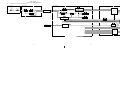
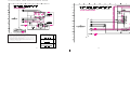
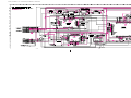
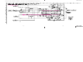
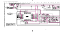
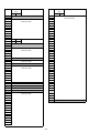
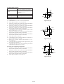
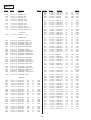
CVX-V1/V1P
SERVICE MANUAL
US Model
Canadian Model
CVX-V1
AEP Model
UK Model
CVX-V1P
Photo: CVX-V1P
NTSC model: CVX-V1
PAL model : CVX-V1P
SPECIFICATIONS
COLOR VIDEO CAMERA
MICROFILM
SAFETY-RELATED COMPONENT WARNING!!
ATTENTION AU COMPOSANT AYANT RAPPORT
À LA SÉCURITÉ!
COMPONENTS IDENTIFIED BY MARK ! OR DOTTED
LINE WITH MARK ! ON THE SCHEMATIC DIAGRAMS
AND IN THE PARTS LIST ARE CRITICAL TO SAFE
OPERATION. REPLACE THESE COMPONENTS WITH
SONY PARTS WHOSE PART NUMBERS APPEAR AS
SHOWN IN THIS MANUAL OR IN SUPPLEMENTS PUBLISHED BY SONY.
LES COMPOSANTS IDENTIFIÉS PAR UNE MARQUE !
SUR LES DIAGRAMMES SCHÉMATIQUES ET LA LISTE
DES PIÈCES SONT CRITIQUES POUR LA SÉCURITÉ
DE FONCTIONNEMENT. NE REMPLACER CES COMPOSANTS QUE PAR DES PIÈCES SONY DONT LES
NUMÉROS SONT DONNÉS DANS CE MANUEL OU
DANS LES SUPPLÉMENTS PUBLIÉS PAR SONY.
SAFETY CHECK-OUT
After correcting the original service problem, perform the following
safety checks before releasing the set to the customer.
1. Check the area of your repair for unsoldered or poorly soldered connections. Check the entire board surface for solder
splashes and bridges.
4. Look for parts which, through functioning, show obvious signs
of deterioration. Point them out to the customer and recommend their replacement.
2. Check the interboard wiring to ensure that no wires are
“pinched” or contact high wattage resistors.
5. Check the B+ voltage to see it is at the values specified.
6. Flexible Circuit Board Repairing
3. Look for unauthorized replacement parts, particularly transistors, that were installed during a previous repair. Point them
out to the customer and recommend their replacement.
• Keep the temperature of the soldering iron around 270 °C
during repairing.
• Do not touch the soldering iron on the same conductor of
the circuit board (within 3 times).
• Be careful not to apply force on the conductor when soldering or unsoldering.
–2–
TABLE OF CONTENTS
Section
1.
Title
Page
Section
1-3.
GENERAL ................................................................... 1-1
2.
DISASSEMBLY
2-1.
2-2.
2-3.
2-4.
2-5.
Removal of Cabinet (Lower) Assembly ........................
Removal of VA-103 Board .............................................
Removal of Camera Head Assembly,
CS-53 Board ..................................................................
Removal of Lens (CCD) Assembly ...............................
Circuit Boards Location .................................................
3.
BLOCK DIAGRAMS
3-1.
3-2.
3-3.
3-4.
3-5.
Overall Block Diagram ...................................................
Camera (1) Block Diagram ...........................................
Camera (2) Block Diagram ...........................................
Audio Block Diagram .....................................................
Power Block Diagram ....................................................
4.
PRINTED WIRING BOARDS AND
SCHEMATIC DIAGRAMS
4-1.
4-2.
Frame Schematic Diagram ............................................ 4-1
Printed Wiring Boards and Schematic Diagrams ......... 4-4
CD-188 (CCD Imager, Timing Generator)
Printed Wiring Board ..................................................... 4-5
CD-188 (CCD Imager), (Timing Generator)
Schematic Diagrams ..................................................... 4-7
CS-53 (Camera, Y/C Process, Mic Amp,
Mode Control) Printed Wiring Board ............................. 4-11
CS-53 (Camera, Y/C Process)
Schematic Diagram ....................................................... 4-15
CS-53 (Mode Control) Schematic Diagram .................. 4-21
CS-53 (Mic Amp) Schematic Diagram .......................... 4-23
VA-103 (DC-DC Converter, Video/Audio I/O, LANC I/O),
IF-69 (Interface) Printed Wiring Boards ........................ 4-28
VA-103 (DC-DC Converter) Schematic Diagram ......... 4-33
VA-103 (Video/Audio I/O) Schematic Diagram ............. 4-36
VA-103 (LANC I/O), IF-69 (Interface)
Schematic Diagrams ..................................................... 4-39
5.
ADJUSTMENTS
5-1. Camera Section Adjustment .........................................
1-1. Preparations Before Adjustment ...................................
1-1-1. List of Service Tools .................................................
1-1-2. Preparations .............................................................
1-1-3. Precaution ................................................................
1. Setting the Switch ....................................................
2. Order of Adjustment .................................................
3. Subjects ....................................................................
1-1-4. Adjustment Remote Commander ............................
1. Using the Adjustment Remote Commander ............
2. Precaution Upon Using the Adjustment
Remote Commander ................................................
1-1-5. Data Process ............................................................
1-2. Initialization of F Page Data ..........................................
1. Initializing the F Page Data ......................................
2. Modification of F Page Data ....................................
3. F Page Table ............................................................
1.
2.
3.
4.
5.
6.
7.
2-1
2-1
2-1
2-2
2-2
3-1
3-5
3-9
3-11
3-13
Title
Page
Camera System Adjustments ..................................
28 MHz Origin Oscillation Adjustment .....................
Picture Frame Setting ..............................................
Color Reproduction Adjustment ...............................
Auto White Balance Reference Data Input ..............
Auto White Balance Adjustment ..............................
White Balance Check ...............................................
Battery Down Adjustment .........................................
5-9
5-9
5-10
5-11
5-12
5-12
5-13
5-14
6.
REPAIR PARTS LIST
6-1.
6-2.
Exploded Views ............................................................. 6-1
Electrical Parts List ........................................................ 6-2
* The color reproduction frame is shown after the page
of ELECTRICAL PARTS LIST.
5-1
5-1
5-1
5-2
5-3
5-3
5-3
5-3
5-4
5-4
5-4
5-5
5-6
5-6
5-6
5-6
–3–
CVX-V1/V1P
SECTION 1
GENERAL
1-1
1-2 E
CVX-V1/V1P
SECTION 2
DISASSEMBLY
Note: Follow the disassembly procedure in the numerical order given.
2-1. REMOVAL OF CABINET (LOWER)
ASSEMBLY
2-3. REMOVAL OF CAMERA HEAD
ASSEMBLY, CS-53 BOARD
2 Camera head assembly
1 Two tapping
screws
3 Claw
9 Tapping screw
0 Two earth leads
4 Claw
1 Connector (CN301)
(Note1, 2)
3 Three tapping
screws
d
ar
3
-5
Bo
CS
6 Connector
(CN601)
5 Cabinet (lower)
assembly
2 Two tapping screws
8 Flexible flat cable (CN802)
4 CS-53 board
7 Flexible flat cable (CN801)
2-2. REMOVAL OF VA-103 BOARD
Note 1: When remove a connector, don't pull at
wire of connector.
Be in danger of the snapping of a wire.
1 Flexible board
(CN803)
d
ar
03
Bo
1
VA
3 VA-103 board
Note 2: When installing a connector, don't press
down at wire of connector.
Be in danger of the snapping of a wire.
2 Four tapping screws
2-1
2-4. REMOVAL OF LENS (CCD) ASSEMBLY
3 Cabinet
(upper)
2 Two screws (P2)
Note 1: When remove a connector, don't pull at
wire of connector.
Be in danger of the snapping of a wire.
5 Screw (M1.7 × 3)
6 Two connectors
(CN101, 102)
(Note1, 2)
7 Connection cord
8 Lens (CCD)
assembly
Note 2: When installing a connector, don't press
down at wire of connector.
Be in danger of the snapping of a wire.
1 Y holder
assembly
4 Two guide holders
2-5. CIRCUIT BOARDS LOCATION
CD-188
CCD IMAGER,
TIMING GENERATOR
(
)
CD
Bo -18
ar 8
d
VA-103
VIDEO/AUDIO I/O,
DC-DC CONVERTER,
LANC I/O
(
)
d
ar
d
Bo rd
ar
oa
Bo
1
B
69
VA -53
IFCS
03
2-2 E
CS-53
CAMERA, Y/C PROCESS,
MIC AMP, MODE CONTROL
(
IF-69
(INTERFACE)
)
CVX-V1/V1P
SECTION 3
BLOCK DIAGRAMS
3-1. OVERALL BLOCK DIAGRAM
LENS BLOCK
CD-188 BOARD
CS-53 BOARD
(SEE PAGE 4-7 - 4-9)
(SEE PAGE 4-15 - 4-24)
VA-103 BOARD
(SEE PAGE 4-33 - 4-41E)
IC307
IC701
MANUAL
FOCUS
LENS
AD0-9
CAMERA
Y
PROCESS
HD, VD
CAMERA
C
PROCESS
IC305
MANUAL
IRIS
IC001
CCD
IMAGER
IC002
BUFFER
CCD OUT
CCD OUT
TG SO, SCK
V1-V4
H1, H 2
RG, XSHT
IC101
TIMING
GENERATOR
S/H
AGC
2m
CAMERA CABLE
A/D
CONV.
8FSC
CLPDM
CLPDM
CAM C
CAM C
Y/C MIX
VIDEO AMP
IC306
TIMING
GENERATOR
S-Y
S-C
S-Y
S-C
IC304
8FSC
PHASE
ADJUST
J701
CAM Y
TG SO, SCK
IC302, 303, 309
310, 311, 312, 303
HD
VD
8FSC
CAM Y
VIDEO
VIDEO
Y OUT
AUDIO L
C OUT
AUDIO R
S VIDEO
VIDEO
L
AUDIO
R
EVR
(D/A CONVERTER)
IF-69 BOARD
(SEE PAGE 4-41E)
05
Y OUT
IC502
C OUT
IC501
AUDIO L
AUDIO R
CAM SI, SO, SCK
CAMERA/MODE
CONTROL
EEPROM
ID2
3.2V
IC802, 803
MUTE
CONTROL
MUTE
LANC I/O
EASY
CONNECTOR
IC801
MUTE
LANC I/O
KEY AE, SW WIND RED, SW AE LOCK
LANC
I/O
LANC SIG
LANC SIG
BATT SIG
ID1
DD ON
UNREG
RESET
IC702
IC401
CONTROL SWITCH BLOCK
(
MIC
PLUG IN
POWER
EXT MIC L, R
)
AUDIO L, R
MIC
AMP
ALC
SW 1
POWER SW
SW_UNREG
POWER
F601
RESET
EVER 3.2V
DD ON
INITIAL RESET
BACKUP VCC
SW 2
KEYAE, SW WIND RED, SW AELOCK
WB SW
WB LOCK
IC602
SW 3
15V
AE SW
AE LOCK
SHUTTER
DIAL
SHUTTER
–7.0V
DC-DC
CONVERTER
3.2V
BATTERY
TERMINAL
IC601
BATT (+)
BATT SIG
4.9V
3-1
BATT (–)
3-2
3-3
CVX-V1/V1P
CVX-V1/V1P
3-2. CAMERA (1) BLOCK DIAGRAM
CS-53 BOARD
CD-188 BOARD
(SEE PAGE 4-15 - 4-24)
(SEE PAGE 4-7 - 4-9)
3.2 Vp-p
0.9 Vp-p
1.0 Vp-p
H
IC001
IC002
CCD IMAGER
7
3
CN102
CCD OUT
6
2
0.14 usec
S/H, AGC, A/D CONVERTER
IC305
IC305 26
BUFFER
CCD OUT
IC305
2
IC307
10
LPF
1
26
BUFFER
PHASE ADJUST
27
DIN
S/H
PIN
AGC
S/H
BLK
DRV
D0-D9
A/D
CONV.
11
ı 10
2
10
23
CK
5
7
5
V2
3
25
V2
AHD 44
1
4
V3
2
28
V3
AVD 45
3
2
V4
1
31
V4
1
8
13
H2
14
22
H2
H1
13
21
H1
RG
12
SHT
10
18
33
RG
XSHT
CLPDM
SSI 38
SSK
RST
30
VL
VDD
11
8
5
SEN 39
7
37
6
40
15V
–7.0V
29
VL
15V
27
VH
10
13
VDD 19
20
43
12
11
AHD
LPF
4
1
2
IC310
7
AVD
CS TG2
2
D
Q
5
2
D
Q
5
1
Q
CK
CLR
3
1
Q
CK
CLR
3
TG SO
7
6
4
2
1
6
D
CLPOB 20
XSHP
Q
Q
CK
CLR
12 17 33 43
5
CAMERA
C PROCESS
D/A
CONV.
IOC
80
AGC CONT1
30
PBLK
AGC CONT2
29
19
ADCLK
REFSLOW
16
44
MCK
3
3.2V
75
CCDCKH
78
CCDCKL
76
PBLK
OSC O
3Vp-p
73
I MUTE
IC309
BUFFER
20
BUFFER
CN303
CAM Y
2.3 Vp-p
74
XSGI
77
ID
0.6 Vp-p
3.2V
OSC I
IC307 20
2.3 Vp-p
17.734475 MHz
63
62
V
XVI
2
4
IC502
IC307 63
CAMERA/MODE CONTROL
1
Q503
CVX-V1P
V=60 Hz: CVX-V1
V=50 Hz: CVX-V1P
VD
51
62 CAM VD
IC307 51
FLD
53
63 FLD
SYSV
65
55 SOFTV
IC305 16
IC304
2
56
AHD
57
AVD
TIMING GENERATOR
7
X301
28.636MHz: CVX-V1
28.375MHz: CVX-V1P
5
4
CK
OSCO
OSCI
CLPDM
1
XSHP 15
XSHD 16
PBLK
2
CCDCLKH 11
27
VREF Y
16
VREF C
VRI
55
SCK
67
SI
68
XCE
69
SO
70
XCLR
71
5
H
MUTE
60
LANC IN
1
14.318 MHz: CVX-V1
14.187 MHz: CVX-V1P
3.2V
IC303
7
CAM C
X302
17.734475MHz
6
TG SCK
23
8
21
22
39
58
64
79
92
CLPI
XSHD
VDD
PR
1
2
21
22
IC313
PR
PR
CK CONT
IC311
7
4
05
IC312
CN101
VM
–7.0V
10
8FSC
IOY
CLPDM
MCK
V1
D/A
CONV.
Q303
AHD
26
CAMERA
Y PROCESS
S/H
IC302
TIMING GENERATOR
4
IC307 23
Q302
83
ı
91
93
IC101
V1
CAMERA Y.C PROCESS
Q301
CN301
4
H
RST SG
CAM SCK
CAM SO
CS CAM
CAM SI
RST CAM
4
RST CAM
7
RST SG
LANC OUT
2
MUTE
LANC IN
LANC OUT
33 CAM SI
34 CAM SO
WB MODE
18
SW AE LOCK
15
KEY AE
82
XTAL
40
MCK
SW WIND RED 15
SW AE LOCK
16
KEY AE
14
29 CS EEPROM
XV1 41
1.8 Vp-p
ID 48
28.636 MHz: CVX-V1
28.375 MHz: CVX-V1P
IC304 4
3.2V
10
13
19 VDD
20
43
15V
30 VM
0.2 Vp-p
IC304 11
AVD 45
SSI 38
29 VL
27 VH
D/A CONVERTER
AHD 44
SSK 37
–7.0V
31 BUSY EEPROM
IC306
14.318 MHz: CVX-V1
14.187 MHz: CVX-V1P
SEN 39
RST 40
12
AGC CONT1
VREF Y
4
13
AGC CONT2
VREF C
5
IC501
20 MHz
99 CS TG2
CS CAM
18
RST CAM
VSK 33
VSI 34
VEN 35
FRQ
LD
15
CLK
16
DI
17
VDD
10
11
STBY DA
CAM SCK
CAM SCK
CAM SO
CAM SO
CAM SI
3.2V
2
SK
XCS 1
3
DI
RST 6
3-6
41
4
DO
BUSY 7
8
CS EEPROM
46 TG SCK
32KHz IN
52
WEN EEPROM
BUSY EEPROM
3.2V
X501
32.768KHz
59 FLIP
32KHz OUT
3-7
3-8
53
0.7 Vp-p
25 CK CONT
50 I MUTE
3-5
EXTAL
45 TG SO
CAM SCK
CAM SO
X502
20MHz
IC502 41
EEPROM
18
98 CS CAM
26 WEN EEPROM
0.8 Vp-p
17
97 STBY DA
35 CAM SCK
XSG1 32
12
32 kHz
VDD
42
51
77
86
87
AVREF
75
76
IC502 52
3.2V
CAMERA BLOCK 2
VA-103 BOARD
CN801
(SEE PAGE 3-9)
CVX-V1/V1P
3-3. CAMERA (2) BLOCK DIAGRAM
3-4. AUDIO BLOCK DIAGRAM
VA-103 BOARD
1.1 Vp-p
(SEE PAGE 4-33 - 4-41E)
0.46 Vp-p
H
IC701
IC701 22
FL701
Q708
LPF
BUFFER
H
H
IC701 31
IC701
BPF
(SEE PAGE 4-37)
IC401
MIC AMP
IC702 ALC
J701
22
CLAMP
6dB
MUTE
31
6dB
18
S-Y
9
6
3
CAM C
VA-103 BOARD
Y/C MIX, VIDEO AMP
EQ
S VIDEO
L/R
MIX
INT
HPF
13
16
BUFFER
6dB
MUTE
2
S-C
14
CN303
AUDIO L
J701
CN801
2
29
13
AMP
1
AUDIO L
L
EXT
4
Q707
26
CS-53 BOARD
(SEE PAGE 4-21,4-23)
9
1
CN801
CAM Y
24
1.8 Vp-p
Q706
6dB
VIDEO
6
H
13
(
IF-69 BOARD
VIDEO
(SEE PAGE 4-41E)
0.5 Vp-p
MIC
PLUG IN
POWER
2
)
Q703
IC701 16
1
BUFFER
4.9V
CN802
CAM Y
CN902
Y OUT
CN901
11
6
19
MUTE
IC801
H
Q704
IC701 6
BUFFER
CAM C
9
C OUT
9
14
13
10 DATA
12
LANC SIG
LANC SIG 11
2
LANC SIG
2
17
Q705
4.9V
20
EASY
CONNECTOR
EQ
L/R
MIX
17
HPF
IF-69 BOARD
(SEE PAGE 4-41E)
EXT
AUDIO R
3
28
AUDIO L
INT
CN901
CN802
7
10
CN902
AUDIO L
6
8
7
CN805
LANC SIG
1
H
SW WIND RED
4.9V
(FOR CHECK)
IC502
SW2
SW AE LOCK
CN803
WIND SW1
ON
AUDIO R
KEY AE
AUDIO R
5
Q701
WIND RED
91
OFF
AE LOCK
13
12
11
CAMERA/MODE CONTROL
WB LOCK
SW3
SW AE LOCK
6
OFF
8
ON
EASY
CONNECTOR
Q702
CONTROL SWITCH BLOCK
KEY AE
R
DATA
IC701 14
15
AUDIO R
EQ
1.0 Vp-p
16
7
5
24
LANC OUT
AMP
25
29
LANC I/O
LANC IN
9
3
2.1 Vp-p
CAMERA BLOCK 1
CS-53 BOARD
CN303
(SEE PAGE 3-8)
EQ
EX MIC
DETECT
10 27 30
AUDIO
LEVEL
DETECT
J401
MUTE
SHUTTER
DIAL
60
12
19
Q709
MUTE
CONTROL
SHUTTER
05
05
3-9
3-10
3-11
3-12
CVX-V1/V1P
3-5. POWER BLOCK DIAGRAM
(FOR CHECK)
2
VA-103 BOARD
IF-69 BOARD (SEE PAGE 4-41E)
CN805
(SEE PAGE 4-33 - 4-41E)
LANC DC
CN802
UNREG
BATTERY
TERMINAL
IC801
CN601
BATT (+)
1 UNREG
2
BATT SW (–)
Q604
IC602
3
BATT (–)
16
1
VIN
7
5
UNREG
LANC DC 14
VCC 8
3
14
4
13
CN902
L901
LANC I/O
18
19
EASY
CONNECTOR
ID2
17
ID1
11
CS-53 BOARD
(SEE PAGE 4-15 - 4-24)
Q803
PHASE ADJUST
INITIAL RESET
BACKUP VCC
D604
4
BATT SIG
2
F601
1
BATT SW (+)
CN901
15
CONTROL SWITCH BLOCK
CN803
VOUT 6
1
IC802
RESET 5
2
MUTE CONTROL
1
BATT SENS
MUTE
3
4
2
IC307
POWER
ON
OFF
L601
DC-DC CONVERTER
IC304
IC311
IC309
IC312
CD-188 BOARD
(SEE PAGE 4-7 - 4-9)
IC306
IC803
11
MUTE CONTROL
IC601
IC310
L303
POWER
5
D803
IC302
CAMERA
Y.C
PROCESS
SW 1
Q801
VCC 5
LED 1
POWER
LED
1
VCC 5
2
4
SHUTTER
DIAL
L302
SHUTTER
EVR
D/A CONV.
DD ON
D802
VCC 28
IC305
L301
Q603
SWITCHING
IC313
IC304
D602
22 CT
21 RT
CN801
Q605
SWITCHING
EVER3.2V
FB4 18
3.2V
T601
OUTPUT VCC13 43
OUTPUT VCC24 31
CO 13
2
D603
Q601
SWITCHING
3
6
1
4
IC401
CN303
3
28
6
25
7
24
5
26
4
27
TIMING
GENERATOR
L401
EVER3.2V
CCD
IMAGER
TIMING
GENERATOR
OUTPUT-4 37
MOSGATE-4 60
IC001
IC101
S/H AGC
A/D CONV.
MIC AMP
IC002
3.2V
CN301
3.2V 9
3.2V
CN101
4 3.2V
BUFFER
4.9V
Q607-610
–7.0V
REG
–7.0V
L605
15V
OUTPUT-3 36
–7.0V
15V
–7.0V
–7.0V
15V
15V
8
3
7
2
–7.0V
15V
L001
EMERGENCY
DETECT
3
Q606
FB3 34
IC502
Q602
SWITCHING
OUTPUT-2 50
FB2 35
CAMERA/MODE CONTROL
L602
D601
4.9V
L701
IC701
Y/C MIX
VIDEO AMP
L702
IC702
LED PWR
BATT SENS
ALC
MUTE
RESET
STBY3 29
SYBT 30
VREF 37
DD ON
BATT SIG
4.9V
8
23
12
19
18
13
19
12
20
11
21
10
22
9
LED PWR
BATT SENS
MUTE
RESET
DD ON
BATT SIG
89
LED PWR
71
BATT SENS
60
MUTE
38
RESET
37
DD ON
48
BATT SI
49
BATT SO
L501
IC501
EEPROM
Q501
OUTPUT VCC56 63
Q502
05
3-13
3-14
3-15
3-16 E
CVX-V1/V1P
SECTION 4
PRINTED WIRING BOARDS AND SCHEMATIC DIAGRAMS
4-1. FRAME SCHEMATIC DIAGRAM
FRAME
4-1
4-2
4-3
CVX-V1/V1P
CD-188 (CCD IMAGER), (TIMING GENERATOR) SCHEMATIC DIAGRAM
CD-188 BOARD (2/2)
4
7 Vp-p
H
IC101 @∞, @§
5
7 Vp-p
H
IC101 @•, #¡
6
3 Vp-p
H
IC101 $¢
7
3 Vp-p
V
IC101 $∞
CD-188 BOARD (1/2)
Precautions for Replacement of CCD Imager
• The CD-188 board mounted as a repair part is not equipped
with a CCD imager.
When replacing this board, remove the CCD imager from the
old one and mount it onto the new one.
• If the CCD imager has been replaced, carry out all the
adjustments for the camera section.
• As the CCD imager may be damaged by static electricity from
its structure, handle it carefully like for the MOS IC.
In addition, ensure that the receiver is not covered with dusts
nor exposed to strong light.
1
7 Vp-p
H
IC001 1, 2
2
7 Vp-p
H
IC001 3, 4
3
1.0 Vp-p
H
IC001 7
CCD IMAGER TIMING GENERATOR
4-7
4-8
4-9
4-10
CD-188 (1/2)
/
CD-188 (2/2)
CVX-V1/V1P
CS-53 (CAMERA, Y/C PROCESS, MIC AMP, MODE CONTROL) PRINTED WIRING BOARD
– Ref. No.: CS-53 board; 1,000 series –
•
•
•
For printed wiring board.
CS-53 board is 4-layers print board. However, the patterns of
layers 2 to 3 have not been included in the diagram.
Chip transistor
C
B
There are few cases that the part isn't mounted in this model is printed on this diagram.
E
CS-53 BOARD(SIDE B)
CS-53 BOARD(SIDE A)
J401
A
A
B
B
5
8
C
)
G
7
10
6
4
(
MIC
PLUG IN
POWER
13
9
12 11
G
S
1
2
C
D
3
12
1-669-61205
1
2
3
4
5
6
7
8
1
CS-53 BOARD (SIDE A)
< CAPACITOR >
4-11
CAMERA, Y/C PROCESS, MIC AMP, MODE CONTROL
CS-53
C302
C309
C310
C312
C315
C317
C319
C320
C321
C322
C323
C324
C325
C326
C327
C328
C331
C332
C333
C334
C335
C-5
B-5
B-6
B-6
B-5
C-5
C-5
C-5
C-5
C-5
C-6
C-5
C-5
C-6
C-6
C-6
B-6
C-7
C-7
B-7
C-7
C336
C337
C338
C339
C340
C341
C342
C343
C403
C404
C405
C406
C407
C408
C409
C410
C411
C412
C413
C414
C415
C416
C417
C-7
B-7
C-7
B-7
B-8
C-7
C-8
C-8
B-3
B-4
C-2
C-3
C-4
C-3
C-4
C-4
C-4
C-3
C-3
C-4
C-4
C-4
C-3
C418
C419
C420
C421
C422
C423
C424
B-3
B-4
B-3
B-4
B-3
B-4
B-3
< DIODE >
D302
D501
A-7
C-8
< FERRITE BEAD >
FB316
4-12
C-4
C-3
C-4
< COIL >
L301
L303
L401
B-6
C-6
B-4
< TRANSISTOR >
Q301
Q502
C-5
C-8
B-6
< RESISTOR >
C-6
C-7
C-5
C-3
R310
R313
R324
R325
R326
R327
< IC >
IC305
IC307
IC309
IC310
IC312
IC313
IC401
B-5
B-6
B-7
B-7
B-7
C-7
R328
R329
R330
R331
R332
R334
R335
R350
R401
R402
R405
R406
R407
R408
R409
R410
R411
R412
R413
R414
R415
R416
R417
B-7
B-7
C-7
B-7
C-7
C-8
B-8
B-7
C-3
C-3
C-4
C-4
C-4
C-4
C-3
B-3
C-3
C-3
C-4
B-4
B-3
C-3
B-4
1-669-612-
05
R418
R419
R420
R421
R422
R508
R509
R510
R517
(
B-4
B-3
B-3
B-3
B-4
B-8
B-8
B-8
C-8
< VIBRATOR >
X302
X501
CD-188
CCD IMAGER,
TIMING GENERATOR
B-6
C-8
2
(
)
4
5
6
7
8
CS-53 BOARD (SIDE B)
)
CD
Bo -18
ar 8
d
VA-103
VIDEO/AUDIO I/O,
DC-DC CONVERTER,
LANC I/O
3
12
rd
oa
d
ar
3 B ard
o
Bo
10
B
69
VA -53
IFS
C
CS-53
CAMERA, Y/C PROCESS,
MIC AMP, MODE CONTROL
(
IF-69
(INTERFACE)
4-13
)
< CAPACITOR >
< CONNECTOR >
< IC >
C301
C305
C306
C308
C311
C313
C314
C316
C318
C330
C347
C501
C502
C503
C504
C505
C506
C509
C510
C511
C512
CN301
CN303
IC302
IC303
IC304
IC306
IC311
IC501
IC502
B-5
C-4
B-4
B-4
C-5
C-5
C-5
C-5
C-6
B-3
C-6
B-1
C-1
C-2
C-3
C-2
C-3
C-1
C-1
B-3
C-3
C-7
A-2
< FERRITE BEAD >
FB301
FB302
FB303
FB313
FB314
FB315
FB401
FB402
FB403
C-7
C-7
C-7
B-4
C-5
C-6
C-8
C-8
C-7
< FILTER >
FL301
FL302
C-6
B-6
Q501
C-6
C-6
C-4
C-3
C-6
B-1
B-2
< JACK >
J401
C-8
< COIL >
L302
L501
B-3
C-3
< TRANSISTOR >
Q302
Q303
4-14
B-3
B-3
C-1
< RESISTOR >
R302
R303
R304
R305
R306
R307
R308
R312
R314
R316
R317
R338
R339
R423
R424
R501
R502
R503
R504
C-6
C-6
C-6
B-6
C-6
C-6
B-5
C-5
C-5
C-4
C-5
A-2
A-3
B-7
B-7
B-1
B-1
A-2
B-1
R505
R506
R507
R511
R514
R515
R516
R518
R519
R520
R522
R523
R524
R526
R528
R529
R530
R531
B-2
B-2
B-2
B-1
C-1
C-1
C-1
C-1
C-2
C-1
C-1
C-2
C-2
B-1
B-2
B-2
B-2
C-2
< VARISTOR >
VDR401 C-8
VDR402 C-8
< VIBRATOR >
X301
X502
C-5
C-1
CVX-V1/V1P
CS-53 (CAMERA, Y/C PROCESS) SCHEMATIC DIAGRAM
CS-53 BOARD (1/3)
6
1
1.8 Vp-p
1.0 Vp-p
14.318 MHz: NTSC
14.187 MHz: PAL
H
IC305 @§
IC304 !¡
2
7
0.8 Vp-p
3 Vp-p
V=60Hz: NTSC
V=50Hz: PAL
V
28.636 MHz
IC304 5
IC307 %¡
3
8
0.8 Vp-p
0.6 Vp-p
28.636 MHz: NTSC
28.375 MHz: PAL
H
IC304 4
IC307 @º
4
9
0.9 Vp-p
0.9 Vp-p
14.318 MHz: NTSC
14.187 MHz: PAL
H
IC307 @£
IC305 !§
10
5
PAL
2.3 Vp-p
3.2 Vp-p
17.734475 MHz
0.14usec
IC307 ^£
IC305 2 – 0
NTSC model: CVX-V1
PAL model : CVX-V1P
CAMERA, Y/C PROCESS
4-15
4-16
4-17
4-18
CS-53 (1/3)
CVX-V1/V1P
CVX-V1/V1P
CS-53 (MODE CONTROL) SCHEMATIC DIAGRAM • See page 4-11 for CS-53 BOARD printed wiring board.
CS-53 BOARD (2/3)
11
3 Vp-p
V
V=60Hz: NTSC
V=50Hz: PAL
IC502 ^™
12
0.7 Vp-p
32.768 kHz
IC502 %™
13
0.2 Vp-p
20 MHz
IC502 $¡
NTSC model: CVX-V1
PAL model : CVX-V1P
MODE CONTROL
CS-53 (2/3)
4-20
4-21
4-22
CVX-V1/V1P
CS-53 (MIC AMP) SCHEMATIC DIAGRAM
• See page 4-11 for CS-53 BOARD printed wiring board.
MIC AMP
4-23
4-24
CS-53 (3/3)
CVX-V1/V1P
CVX-V1/V1P
•
•
VA-103 (DC-DC CONVERTER, VIDEO/AUDIO I/O, LANC I/O), IF-69 (INTERFACE) PRINTED WIRING BOARDS
– Ref. No.: VA-103 board; 1,000 series, IF-69 board; 1,000 series –
•
For printed wiring boards.
VA-103 board is 4-layers print board. However, the patterns of
layers 2 to 3 have not been included in the diagram.
Chip transistor
C
B
There are few cases that the part isn't mounted in this model is printed on this diagram.
OUTPUT
E
S VIDEO
C
G
VA-103 BOARD(SIDE B)
VA-103 BOARD(SIDE A)
Y
G
VIDEO
R
IF-69 BOARD (SIDE A)
A
A
IF-69 BOARD (SIDE B)
A
A
B
B
C
C
B
B
5
D
3 4
1
C
C
7
2
1-669-614-
1
05
2
CD-188
CCD IMAGER,
TIMING GENERATOR
(
VA-103
VIDEO/AUDIO I/O,
DC-DC CONVERTER,
LANC I/O
)
3
4
5
6
7
13
8
)
< CAPACITOR >
CS-53
CAMERA, Y/C PROCESS,
MIC AMP, MODE CONTROL
(
d
ar
d
Bo rd
ar
a
o
Bo
1
B
69
VA -53
IFS
C
03
C625
C627
C628
C701
C702
C713
C714
C716
C718
C720
C721
C724
C725
C729
C730
C733
C735
C738
C739
)
IF-69
(INTERFACE)
4-28
B-7
B-6
B-7
B-2
B-3
C-3
C-2
B-5
B-4
C-2
C-2
C-2
C-3
B-2
B-2
B-5
C-4
C-2
B-2
6
D
1-669-614-
05
1
2
3
4
5
6
< CAPACITOR >
< CONNECTOR >
CN601
CN801
CN802
CN803
CN805
C-8
A-7
C-5
C-4
C-1
< COIL >
L601
L602
L603
L605
L702
C-6
C-6
C-6
B-7
C-3
Q610
Q701
Q702
Q704
Q708
Q709
Q801
B-8
B-1
B-3
B-6
C-5
B-3
C-4
< DIODE >
< LINE FILTER >
< RESISTOR >
D603
LF601
R620
R621
R622
R623
R624
R625
R626
R627
R702
R703
R704
R710
B-7
< IC >
< FUSE >
F601
C-8
C-8
IC702
C-2
< FILTER >
< TRANSISTOR >
FL701
Q606
Q607
Q608
Q609
C-4
B-7
B-7
B-7
B-8
B-7
B-7
B-7
B-7
B-7
B-8
B-8
B-8
B-6
C-2
C-3
C-2
R713
R715
R716
R717
R718
R719
R720
R721
R722
R723
R726
R727
R729
R733
R735
R736
R737
R738
R739
R804
R805
R806
B-2
C-3
C-3
C-2
C-2
C-2
C-2
C-2
B-5
B-6
C-4
C-4
C-4
C-4
C-2
C-3
C-3
C-2
B-2
C-3
C-4
C-4
R809
R810
R815
C-6
C-6
C-5
C602
C603
C604
C605
C606
C607
C608
C609
C610
C611
C612
C613
C614
C618
C619
C620
C621
C622
C623
C624
< TRANSFORMER >
T601
C-7
< VARISTOR >
VDR601 B-8
VDR602 C-8
A-2
B-2
A-2
B-2
B-2
B-2
B-1
B-1
B-1
B-1
C-2
C-2
C-2
C-3
B-1
C-3
C-3
C-3
C-3
C-2
C626
C629
C703
C704
C705
C706
C707
C708
C709
C710
C711
C712
C715
C717
C719
C734
C736
C737
C801
C802
C803
C805
C-1
B-1
C-4
C-5
C-5
B-4
C-4
C-4
C-4
C-4
C-4
B-4
B-4
B-4
C-5
C-3
B-3
B-3
C-6
C-6
C-6
A-1
< DIODE >
D601
D602
D604
D801
D802
D803
C-2
C-2
C-1
C-6
A-2
A-2
IC602
IC701
IC801
IC802
IC803
7
C-1
C-5
C-6
A-1
A-2
< JACK >
J701
A-5
Q604
Q605
Q703
Q705
Q706
Q707
Q803
C-1
C-2
C-4
B-7
B-6
B-4
B-4
1
8
< RESISTOR >
< FERRITE BEAD >
< COIL >
FB701
FB702
FB703
FB704
FB705
FB706
FB707
B-4
B-4
B-3
B-5
B-6
B-7
B-6
< IC >
IC601
B-2
L604
L606
L701
L703
C-2
C-2
C-4
B-3
< TRANSISTOR >
Q601
Q602
Q603
C-2
C-2
C-2
R601
R602
R603
R604
R606
R607
R608
R609
R610
R611
R612
R613
B-2
A-2
B-2
B-2
B-2
B-1
B-1
B-3
B-1
B-1
C-2
C-2
R614
R615
R616
R618
R619
R701
R705
R706
R707
R708
R709
R711
R712
R724
R725
R728
R730
R731
R732
R801
R802
R803
1-669-613-
13
VA-103 BOARD (SIDE B)
VA-103 BOARD (SIDE A)
CD
Bo -18
ar 8
d
(
AUDIO
L
C-1
C-1
C-1
C-1
C-1
B-3
B-6
B-6
B-5
B-5
B-4
B-4
B-5
C-4
C-4
B-3
B-4
B-3
B-4
C-6
C-6
C-6
R811
R812
R813
R814
A-2
A-2
A-2
A-2
2
11
D
1-669-613- 11
3
1
/
IF-69
4-29
4-30
4-31
3
IF-69 BOARD (SIDE A)
IF-69 BOARD (SIDE B)
< CONNECTOR >
< CONNECTOR >
< VARISTOR >
CN902
CN901
VDR901
VDR902
VDR903
VDR904
VDR905
VDR906
VDR907
A-2
C-2
< FERRITE BEAD >
< VARISTOR >
VDR701
VDR702
VDR703
VDR704
VDR705
FB901
FB902
FB903
FB905
FB906
B-5
B-4
B-4
B-7
B-6
B-2
B-2
B-2
B-2
B-2
< COIL >
L901
C-3
< RESISTOR >
R901
DC-DC CONVERTER, VIDEO/AUDIO I/O, LANC I/O INTERFACE
VA-103
2
4-32
B-2
C-2
C-2
C-2
C-2
C-2
C-2
D-2
CVX-V1/V1P
VA-103 (DC-DC CONVERTER) SCHEMATIC DIAGRAM
VA-103 BOARD (1/3)
1
13 Vp-p
2.0 µsec
Q601 C
DC-DC CONVERTER
4-33
4-34
4-35
VA-103 (1/3)
CVX-V1/V1P
VA-103 (VIDEO/AUDIO I/O) SCHEMATIC DIAGRAM
• See page 4-28 for VA-103 BOARD printed wiring board.
VA-103 BOARD (2/3)
2
0.46 Vp-p
H
IC701 @™
3
0.5 Vp-p
H
IC701 !§
4
1.0 Vp-p
H
IC701 !¢
5
1.8 Vp-p
H
IC701 9
6
2.1 Vp-p
H
IC701 6
7
1.1 Vp-p
H
IC701 #¡
VIDEO/AUDIO I/O
VA-103 (2/3)
4-36
4-37
4-38
CVX-V1/V1P
VA-103 (LANC I/O), IF-69 (INTERFACE) SCHEMATIC DIAGRAM
• See page 4-28 for VA-103 BOARD and IF-69 BOARD printed wiring boards.
LANC I/O INTERFACE
4-39
4-40
4-41 E
VA-103 (3/3)
/
IF-69
CVX-V1/V1P
SECTION 5
ADJUSTMENTS
5-1. CAMERA SECTION ADJUSTMENT
NTSC model: CVX-V1
PAL model : CVX-V1P
1-1.
PREPARATIONS BEFORE ADJUSTMENT
1-1-1. List of Service Tools
• Oscilloscope
• Regulated power supply
• Color monitor
• Digital voltmeter
Ref. No.
• Vectorscope
Name
• Frequency counter
Parts Code
Usage
J-1
Filter for color temperature correction (C14)
J-6080-058-A
Auto white balance adjustment/check
White balance adjustment/check
J-2
ND filter 1.0
ND filter 0.3
J-6080-808-A
J-6080-818-A
White balance check
White balance check
J-3
Pattern box PTB-450
J-6082-200-A
J-4
Color chart for pattern box
J-6020-250-A
J-5
Adjustment remote commander
(RM-95 upgraded). Note
J-6082-053-B
J-6
Clear chart for pattern box
J-6080-621-A
J-7
CPC-5 jig
J-6082-351-A
For adjusting the video section
Note: If the microprocessor IC in the adjustment remote commander is not the new microprocessor (UPD7503G-C56-12), the pages
cannot be switched.
In this case, replace with the new microprocessor (8-759-148-35).
J-1
J-2
J-6
J-7
J-3
J-4
Fig. 5-1-1
5-1
J-5
1-1-2. Preparations
Note 1: For details of how remove the cabinet and boards, refer
to “2. DISASSEMBLY”.
Pattern box
1) Connect the equipment for adjustments according to Fig. 5-1-3.
2) Connect the adjustment remote commander to the CN805 on
the VA-103 board via CPC-5 (J-6082-351-A).
L
Front side of the lens
L = About 40 cm
Fig. 5-1-2
Audio (L)
Audio (R)
Color monitor
Vectorscope
75 Ω
terminated
Video
CPC-5jig
(J-6082-351-A)
Remote
terminal
Camera head
Adjustment remote comander
(RM-95)
(J-6082-053-B)
CN805
CN301
Regulated power supply
(8.4 V ± 0.1 Vdc)
Video/Audio
output
terminal
VA-103
board
CN803
CS-53
board
CN802
CN801
CN601
Note 2: In changing data, wait for more than
5 seconds after the set was turned
on, then change the data.
Fig. 5-1-3
5-2
CN303
1-1-3. Precaution
1. Setting the Switch
Unless otherwise specified, set the switches as follows and perform adjustments.
1. POWER switch (Control switch block) .............. ON
2. AE LOCK switch (Control switch block) ........... OFF
2. Order of Adjustments
Basically carry out adjustments in the order given.
Electronic beam scanning frame
A B
A=B
0 ± 0.1msec
Yellow
Cyan
Green
White
Magenta
Red
Blue
Blue
Yellow
Cyan
Green
White
Magenta
Red
H
CRT picture frame
V
B A
Enlargement
Fig. b (TV monitor picture)
Fig. a (Video output terminal
output waveform)
Difference in level
B
Direct the camera toward the subject and place the
subject with the distance (about 40 cm) from camera
until the specified picture frame fills the monitor display as shown in Fig. a and Fig. b.
A
Fig. 5-1-4
3. Subjects
1) Color bar chart (Standard picture frame).
When performing adjustments using the color bar chart, adjust the picture frame as shown in Fig. 5-1-4. (Standard picture frame)
2) Clear chart (Standard picture frame)
Remove the color bar chart from the pattern box and insert a
clear chart in its place. (Do not perform zoom operations
during this time.)
5-3
1-1-4. ADJUSTMENT REMOTE COMMANDER
The adjustment remote commander is used for changing the calculation coefficient in signal processing, EVR data, etc. The adjustment remote commander performs bi-directional communication with the unit using the remote commander signal line (LANC).
The resultant data of this bi-directional communication is written
in the non-volatile memory.
2. Precautions Upon Using
The Adjustment Remote Commander
Mishandling of the adjustment remote commander may erase the
correct adjustment data at times. To prevent this, it is recommended
that all adjustment data be noted down before beginning adjustments and new adjustment data after each adjustment.
1. Using the Adjustment Remote Commander
1) Connect the adjustment remote commander to the CN805
on the VA-103 board via CPC-5 (J-6082-351-A).
2) Set the HOLD switch of the adjustment remote commander
to “HOLD” (SERVICE position). If it has been properly connected, the LCD on the adjustment remote commander will
display as shown in Fig. 5-1-5.
Page
Data
Address
Fig. 5-1-5
3) Operate the adjustment remote commander as follows.
• Changing the page
The page increases when the EDIT SEARCH+ button is pressed,
and decreases when the EDIT SEARCH– button is pressed.
There are altogether 16 pages, from 0 to F.
Hexadecimal
notation
LCD Display
Decimal notation
conversion value
0 1 2 3 4 5 6 7 8 9 A B CD E F
0 1 2 3 4 5 6 7 8 9 A b c d E F
0 1 2 3 4 5 6 7 8 9 10 11 12 1314 15
Table. 5-1-1
• Changing the address
The address increases when the FF ()) button is pressed, and
decreases when the REW (0) button is pressed. There are
altogether 256 addresses, from 00 to FF.
• Changing the data (Data setting)
The data increases when the PLAY (() button is pressed, and
decreases when the STOP (p) button is pressed. There are altogether 256 data, from 00 to FF.
• Writing the adjustment data
The PAUSE button must be pressed to write the adjustment data
(F page) in the nonvolatile memory. (The new adjusting data
will not be recorded in the nonvolatile memory if this step is not
performed.)
4) After completing all adjustments, turn off the main power
supply (8.4V) once.
5-4
1-1-5. DATA PROCESS
The calculation of the DDS display and the adjustment remote
commander display data (hexadecimal notation) are required for
obtaining the adjustment data of some adjustment items. In this
case, after converting the hexadecimal notation to decimal notation, calculate and convert the result to hexadecimal notation, and
use it as the adjustment data. Indicates the hexadecimal-decimal
conversion table.
2
Hexadecimal-decimal Conversion Table
Lower digit of
hexadecimal
0
1
2
3
4
5
6
7
8
9
A
(A)
B
(b)
C
(c)
D
(d)
E
(E)
F
(F)
Upper digit
of hexadecimal
1
0
0
1
2
3
4
5
6
7
8
9
10
11
12
13
14
15
1
16
17
18
19
20
21
22
23
24
25
26
27
28
29
30
31
2
32
33
34
35
36
37
38
39
40
41
42
43
44
45
46
47
3
48
49
50
51
52
53
54
55
56
57
58
59
60
61
62
63
4
64
65
66
67
68
69
70
71
72
73
74
77
76
77
78
79
5
80
81
82
83
84
85
86
87
88
89
90
91
92
93
94
95
6
96
97
98
99
100
101
102
103
104
105
106
107
108
109
110
111
7
112
113
114
115
116
117
118
119
120
121
122
123
124
125
126
127
8
128
129
130
131
132
133
134
135
136
137
138
139
140
141
142
143
9
144
145
146
147
148
149
150
151
152
153
154
155
156
157
158
159
A (A)
160
161
162
163
164
165
166
167
168
169
170
171
172
173
174
175
B (b)
176
178
179
180
181
182
183
184
185
186
187
188
189
190
191
C (c)
192
177
193
194
195
196
197
198
199
200
201
202
203
204
205
206
207
D (d)
208
209
210
211
212
213
214
215
216
217
218
219
220
221
222
223
E (E)
224
225
226
227
228
229
230
231
232
233
234
235
236
237
238
239
F (F)
240
241
242
243
244
245
246
247
248
249
250
251
252
253
254
255
Note: The characters shown in the parenthesis ( ) shown the display on the adjustment remote commander.
(Example) If the DDS display or the adjustment remote commander shows BD (bd);
Because the upper digit of the adjustment number is B (b), and the lower digit is D (d), the meeting point
“189” of 1 and 2 in the above table is the corresponding decimal number.
Table. 5-1-2
5-5
1-2.
3. F Page Table
INITIALIZATION OF F PAGE DATA
Note: Fixed data-1 : Initialized data. ( Refer to “1. Initializing
the F Page Data”.)
Fixed data-2 : Modified data. (Refer to “2. Modification of
F PAGE Data”.)
1. Initializing the F Page Data
Note: If the F page data has been initialized, “Modification of F
PAGE Data” and the camera system adjustments need to
be performed again.
Adjustment page
F
Adjustment Address
00 to FF
Address
Initializing Method:
1) Select page: 6, address: 02, and check that the data is “00”.
2) Select page: 0, address: 01, and set data: 01.
3) Select page: 3, address: 00, set data: 2D (NTSC) or data: 2F
(PAL), and press the PAUSE button of the adjustment remote commander.
4) Select page: 3, address: 01, set data: 2D (NTSC) or data: 2F
(PAL), and press the PAUSE button of the adjustment remote commander.
5) Select page: 6, address: 02, and check that the data is “01”.
6) Select page: 3, address: 00, set data: 00, and press the PAUSE
button of the adjustment remote commander.
7) Select page: 3, address: 01, set data: 00, and press the PAUSE
button of the adjustment remote commander.
8) Select page: 0, address: 01, and set data: 00.
9) Perform “Modification of F Page Data”.
00
01
02
03
04
05
06
07
08
09
0A
0B
0C
0D
0E
0F
10
11
12
13
14
15
16
17
18
19
1A
1B
1C
1D
1E
1F
20
21
22
23
24
25
26
27
28
29
2A
2B
2C
2D
2E
2F
2. Modification of F PAGE Data
If the F PAGE data has been initialized, change the data of the
“Fixed data-2” address shown in the following tables by manual
input.
Modifying Method:
1) Before changing the data, select page: 0, address: 01, and set
data: 01.
2) New data for changing are not shown in the tables because
they are different in destination. When changing the data,
copy the data built in the same model.
Note: If copy the data built in the different model, the camcorder
may not operate.
3) When changing the data, press the PAUSE button of the adjustment remote commander each time when setting new data
to write the data in the non-volatile memory.
4) Check that the data of adjustment addresses is the initial value.
If not, change the data to the initial value.
5) After changing the data, select page: 0, address: 01, and set
data: 00.
5-6
Initial
value
NTSC PAL
Remark
Fixed data2
Fixed data1
(Initialized data)
Fixed data2
Fixed data1
Fixed data2
Fixed data1
Fixed data2
Fixed data1
(Initialized data)
Fixed data2
Fixed data1
(Initialized data)
Address
30
31
32
33
34
35
36
37
38
39
3A
3B
3C
3D
3E
3F
40
41
42
43
44
45
46
47
48
49
4A
4B
4C
4D
4E
4F
50
51
52
53
54
55
56
57
58
59
5A
5B
5C
5D
5E
5F
60
61
62
63
64
65
66
Initial
Remark
value
NTSC PAL
18
18 Auto White Balance
3D
3D Reference Data Input
21
21
39
39
24
24
Fixed data1
00
30 Picture Frame Setting
21
23
Fixed data1
(Initialized data)
20
20
1B
1B
42
42
89
59
89
59
Address
67
68
69
6A
6B
6C
6D
6E
6F
70
71
72
73
74
75
76
77
78
79
7A
7B
7C
7D
7E
7F
80
81
82
83
84
85
86
87
88
89
8A
8B
8C
8D
8E
8F
90
91
92
93
94
95
96
97
98
99
9A
9B
9C
9D
Fixed data2
Fixed data1
28MHz Origin Oscillation Adj.
Fixed data1
(Initialized data)
Fixed data2
Fixed data1
Color Reproduction Adj.
Fixed data1
Color Reproduction Adj.
Fixed data1
(Initialized data)
Auto White Balance Adj.
Fixed data2
Fixed data1
(Initialized data)
94
9B
B3
C8
D3
94
9B
B3
C8
D3
Battery Down Adj.
Fixed data1
(Initialized data)
5-7
Initial
value
NTSC PAL
Remark
Fixed data1
(Initialized data)
Address
9E
9F
A0
A1
A2
A3
A4
A5
A6
A7
A8
A9
AA
AB
AC
AD
AE
AF
B0
B1
B2
B3
B4
B5
B6
B7
B8
B9
BA
BB
BC
BD
BE
BF
C0
C1
C2
C3
C4
C5
C6
C7
C8
C9
CA
CB
CC
CD
CE
CF
D0
D1
D2
D3
D4
Initial
value
NTSC PAL
Remark
Address
Fixed data2
D5
D6
D7
D8
D9
DA
DB
DC
DD
DE
DF
E0
E1
E2
E3
E4
E5
E6
E7
E8
E9
EA
EB
EC
ED
EE
EF
F0
F1
F2
F3
F4
F5
F6
F7
F8
F9
FA
FB
FC
FD
FE
FF
Fixed data1
(Initialized data)
FD
F6
FE
F4
Color Reproduction Adj.
Fixed data2
Fixed data1
(Initialized data)
Fixed data2
Fixed data1
(Initialized data)
Fixed data2
Fixed data1
(Initialized data)
Fixed data2
Fixed data1
Fixed data2
Fixed data1
Fixed data2
Fixed data1
(Initialized data)
Initial
value
NTSC PAL
Remark
Fixed data1
(Initialized data)
Fixed data2
Table. 5-1-3
5-8
1-3.
CAMERA SYSTEM ADJUSTMENTS
1. 28 MHz Origin Oscillation Adjustment
(CS-53 board)
Set the frequency of the clock for synchronization. If deviated, the
synchronization will be disrupted and the color will become inconsistent.
Subject
Not required
Measurement Point
Pin !™ of IC304
Measuring Instrument
Frequency counter
Adjustment Page
F
Adjustment Address
3F
Specified Value
f=14318181 ± 68 Hz (NTSC)
f=14187500 ± 69 Hz (PAL)
Adjusting method:
1) Select page: 0, address: 01, and set data: 01.
2) Select page: F, address: 3F, change the data and set the clock
frequency (f) to the specified value.
3) Press the PAUSE button of the adjustment remote commander.
4) Select page: 0, address: 01, and set data: 00.
• PARTS LOCATION DIAGRAM FOR 28 MHz ORIGIN OSCILLATION ADJUSTMENT
CS-53 BOARD (SIDE B)
24
25
13
12
IC304
36
37
1
48
5-9
2. Picture Frame Setting
Subject
Color bar chart standard picture frame
(40 cm from the front of the lens)
Measurement Point
Video output terminal
Measuring Instrument
Oscilloscope and TV monitor
Adjustment page
F
Adjustment address
36, 37
Specified Value
A = B, C = D, t = 0 ± 0.1 msec
Check on the oscilloscope
1. Horizontal period
A=B
C=D
B
C
A
D
Setting method:
1) Select page: 0, address: 01, and set data: 01.
2) Select page: F, address: 36, and set data: 00, and press the
PAUSE button of the adjustment remote commander.
3) Select page: F, address: 37, and set data: 40, and press the
PAUSE button of the adjustment remote commander.
4) Adjust the camera direction, and set to the specified position.
5) Mark the position of the picture frame on the monitor display, and adjust the picture frame to this position in following adjustments using “Color bar chart standard picture
frame”.
Fig. 5-1-6
Processing after Completing Adjustments:
1) Select page: F, address: 37, and set data: 21 (NTSC) or set
data: 23 (PAL), and press the PAUSE button of the adjustment remote commander.
2) Select page: F, address: 36, and set data: 00 (NTSC) or set
data: 30 (PAL), and press the PAUSE button of the adjustment remote commander.
3) Select page: 0, address: 01, and set data: 00.
2. Vertical period
t=0 ± 0.1msec
V
Fig. 5-1-7
Color on the TV monitor
Color bar chart picture frame
Fig. 5-1-8
5-10
TV monitor picture frame
3. Color Reproduction Adjustment
Adjust the color Separation matrix coefficient so that proper color
reproduction is produced.
Subject
Color bar chart standard picture
frame
Measurement Point
Video output terminal
Measuring Instrument
Vectorscope
Adjustment Page
F
Adjustment Address
44, 46, AA, AB
Specified Value
All color luminance points should
settle within each color reproduction frame.
For NTSC model
R-Y
MG
R
YL
B-Y
B
Adjusting method:
1) Select page: 0, address: 01, and set data: 01.
2) Select page: 2, address: 01, set data: 3D, and press the PAUSE
button of the adjustment remote commander.
3) Select page: F, address: 1A, set data: 3F, and press the PAUSE
button of the adjustment remote commander.
4) Adjust the GAIN and PHASE of the vectorscope, and adjust
the burst luminance point to the burst position of the color
reproduction frame.
5) Change the data of page: F, address: 44, 46, AA and AB, and
settle each color luminance point in each color reproduction
frame.
Note: Be sure to press the PAUSE button of the adjustment remote commander before changing the addresses. If not,
the new data will not be written to the memory.
6) Press the PAUSE button of the adjustment remote commander.
CY
G
Burst position
For PAL mode
Burst position
R-Y
R
MG
YL
Processing after Completing Adjustments:
1) Select page: 2, address: 01, and set data: 00, and press the
PAUSE button of the adjustment remote commander.
2) Select page: 0, address: 01, and set data: 00.
B-Y
B
G
CY
Fig. 5-1-9
5-11
4. Auto White Balance Reference Data Input
Subject
5. Auto White Balance Adjustment
Adjust to the proper auto white balance output data.
If it is not correct, auto white balance and color reproducibility
will be poor.
Clear chart
(Color bar standard picture frame)
Adjustment Page
F
Adjustment Address
30 to 34
Subject
Clear chart
(Color bar standard picture frame)
Note 1: Perform “Color Reproduction Adjustment” before this
adjustment.
Note 2: Check that the data of page: 2, address: 02 is 00. If not,
turn the power of the unit OFF/ON.
Filter
Filter C14 for color temperature
correction
Measuring Instrument
Page 1 displayed data of the
adjustment remote commander
(Note 2)
Adjusting method:
1) Select page: 0, address: 01, and set data: 01.
2) Select page: 2, address: 40, set data: 02, and press the PAUSE
button of the adjustment remote commander.
3) Select page: 2, address: 41, set data: 01, and press the PAUSE
button of the adjustment remote commander.
4) Shoot the clear chart with the color bar standard picture frame,
and wait for 2 seconds.
5) Select page: 2, address: 01, set data: 11, and press the PAUSE
button of the adjustment remote commander.
6) Select page: 2, address: 01, set data: 0D, and press the PAUSE
button of the adjustment remote commander.
(When the standard data is take in, the data will be automatically input to page: F, address: 30 to 34.)
7) Select page: 2, address: 02, and check that the data is “01”.
Adjustment Page
F
Adjustment Address
4A, 4B
Specified Value
R ratio: 2B40 to 2BC0
B ratio: 5E40 to 5EC0
Measurement Point
Note 1: Perform “Auto White Balance Reference Data Input”
before this adjustment.
Note 2: The right four digits of the page 1 displayed data of the
adjustment remote commander.
01 XXXX
Object data
Adjusting method:
1) Place the C14 filter for color temperature correction on the
lens.
2) Select page: 0, address: 01, and set data: 01.
3) Select page: 2, address: 40, set data: 02, and press the PAUSE
button of the adjustment remote commander.
4) Select page: 2, address: 41, set data: 01, and press the PAUSE
button of the adjustment remote commander.
5) Select page: 2, address: 01, set data: 3F, and press the PAUSE
button of the adjustment remote commander.
6) Select page: 0, address: 03, and set data: 04.
7) Select page: F, address: 4A, change the data and adjust the
average value of the page 1 displayed data (Note 2) to the R
ratio specified value.
8) Press the PAUSE button of the adjustment remote commander.
9) Select page: 0, address: 03, and set data: 05.
10) Select page: F, address: 4B, change the data and adjust the
average value of the page 1 displayed data (Note 2) to the B
ratio specified value.
11) Press the PAUSE button of the adjustment remote commander.
Processing after Completing Adjustments:
1) Select page: 2, address: 01, and set data: 00, and press the
PAUSE button of the adjustment remote commander.
2) Select page: 2, address: 41, and set data: 00, and press the
PAUSE button of the adjustment remote commander.
3) Select page: 2, address: 40, and set data: 00, and press the
PAUSE button of the adjustment remote commander.
4) Select page: 0, address: 01, and set data: 00.
5) Perform “Auto White Balance Adjustment”.
Processing after Completing Adjustments:
1) Select page: 2, address: 01, set data: 00, and press the PAUSE
button of the adjustment remote commander.
2) Select page: 2, address: 41, set data: 00, and press the PAUSE
button of the adjustment remote commander.
3) Select page: 2, address: 40, set data: 00, and press the PAUSE
button of the adjustment remote commander.
4) Select page: 0, address: 03, and set data: 00.
5) Select page: 0, address: 01, and set data: 00.
5-12
6. White Balance Check
Subject
Clear chart
(Color bar standard picture frame)
Filter
Filter C14 for color temperature
correction
ND filter 1.0 and 0.3
Measurement Point
Video output terminal
Measuring Instrument
Vectorscope
Specified Value
Fig. 5-1-10. (A) to (C)
R-Y
2mm
B-Y
2mm
Checking method:
1) Check that the lens is not covered with either filter.
2) Select page: 0, address: 01, and set data: 01.
3) Select page: 2, address: 40, set data: 02, and press the PAUSE
button of the adjustment remote commander.
4) Select page: 2, address: 41, set data: 01, and press the PAUSE
button of the adjustment remote commander.
5) Select page: 2, address: 01, set data: 0F, and press the PAUSE
button of the adjustment remote commander.
6) Check that the center of the white luminance point is within
the circle shown Fig. 5-1-10 (A).
7) Select page: 2, address: 01, set data: 00, and press the PAUSE
button of the adjustment remote commander.
8) Select page: 2, address: 01, set data: 23, and press the PAUSE
button of the adjustment remote commander.
9) Place the C14 filter on the lens.
10) Check that the center of the white luminance point settles in
the circle shown Fig. 5-1-10 (B).
11) Remove the C14 filter, and place the ND filter 1.3 (1.0 +
0.3) on the lens.
12) Check that the white luminance point stopped moving, and
then remove the ND filter 1.3.
13) Check that the center of the white luminance point settles
within the circle shown Fig. 5-1-10 (C).
Fig. 5-1-10 (A)
R-Y
1.0mm
B-Y
1.0mm
3mm
3mm
Fig. 5-1-10 (B)
R-Y
3mm
Processing after Completing Adjustments:
1) Select page: 2, address: 41, set data: 00, and press the PAUSE
button of the adjustment remote commander.
2) Select page: 2, address: 40, set data: 00, and press the PAUSE
button of the adjustment remote commander.
3) Select page: 2, address: 01, set data: 00, and press the PAUSE
button of the adjustment remote commander.
4) Select page: 0, address: 01, set data: 00.
3mm
2.0mm
B-Y
1.0mm
Fig. 5-1-10 (C)
5-13
7. Battery Down Adjustment
Set the battery end voltage.
Mode
11) Select page: F, address: 5B, set data: X3, and press the PAUSE
button of the adjustment remote commander.
12) Select page: F, address: 5C, set data: X4, and press the PAUSE
button of the adjustment remote commander.
13) Select page: 0, address: 01, and set data: 00.
Camera on
Subject
Arbitrary
Measurement Point
LCD display of the adjustment
remote commander.
Measuring Instrument
Not required
Adjustment Page
F
Adjustment Address
58 to 5C
Connection
1) Connect the regulated power supply and the digital voltmeter to the battery terminal as shown in Fig. 5-1-11.
Digital voltmeter
Regulated power supply
(6.1±0.1Vdc)
Battery terminal
Fig. 5-1-11
Adjusting method:
1) Adjusting the output voltage fo the regulated power supply
so that the digital voltmeter display is 6.1 ± 0.1 Vdc.
2) Select page: 0, address: 01, and set data: 01.
3) Decrease the output voltage of the regulated power supply
so that the digital voltmeter display is 5.30 ± 0.01 Vdc.
4) Select page: 3, address: 0D, read the data, and this data is
named X0.
5) Convert X0 to decimal notation, and obtain X0'.
(Refer to “Table 5-1-2. Hexadecimal-decimal conversion
table”.)
6) Calculate X1', X2', X3', and X4' using follwing equations (decimal calculation).
Address: 59
X1' = X0' + 8
Address: 5A
X2' = X0' + 32
Address: 5B
X3' = X0' + 53
Address: 5C
X4' = X0' + 64
7) Convert X1', X2', X3' and X4' to hexadecimal notation, and
obtain X1, X2, X3 and X4.
8) Select page: F, address: 58, set data: X0, and press the PAUSE
button of the adjustment remote commander.
9) Select page: F, address: 59, set data: X1, and press the PAUSE
button of the adjustment remote commander.
10) Select page: F, address: 5A, set data: X2, and press the PAUSE
button of the adjustment remote commander.
5-14 E
CVX-V1/V1P
SECTION 6
REPAIR PARTS LIST
6-1.
EXPLODED VIEWS
NOTE:
• -XX and -X mean standardized parts, so they may
have some difference from the original one.
• Color Indication of Appearance Parts
Example:
KNOB, BALANCE (WHITE) . . . (RED)
↑
↑
Parts Color
Cabinet's Color
• Items marked “*” are not stocked since they are
seldom required for routine service. Some delay
should be anticipated when ordering these items.
The components identified by mark
! or dotted line with mark ! are critical for safety.
Replace only with part number specified.
• The mechanical parts with no reference number in
the exploded views are not supplied.
• Accessories are given in the last of the electrical
parts list.
27
Les composants identifiés par une
marque ! sont critiquens pour la
sécurité.
Ne les remplacer que par une pièce
portant le numéro spécifié.
11
11
not
supplied
29
26
15
14
25
13
12
29
23
32
25
rd
oa
24
1
VA
30
*IC001
B
03
22
CVX-V1
33
17
10
28
21
19
9
11
11
16
20
11
7
69
6
IF-
not
supplied
11
8
5
4
not
supplied
11
31
18
rd
oa
B
-53
2
CS
*Be sure to read “Precautions for
Replacement of CCD Imager” on
page 4-7 when changing the CCD
imager.
Ref. No.
Part No.
Description
1
1
2
3
4
A-7073-693-A
A-7073-696-A
1-694-076-21
1-783-522-11
1-783-523-11
5
5
6
7
8
CVX-V1
1
34
3
11
Remark
Ref. No.
Part No.
Description
CS-53 BOARD, COMPLETE (CVX-V1P)
CS-53 BOARD, COMPLETE (CVX-V1)
TERMINAL BOARD, BATTERY
CABLE, FLEXIBLE FLAT (FFC-246)
CABLE, FLEXIBLE FLAT (FFC-247)
17
* 18
19
20
21
1-475-734-11
2-277-426-01
3-050-944-11
1-758-186-11
1-758-157-11
SWITCH BLOCK, CONTROL (VC)
CLAMP
CABINET (LOWER)
LENS, VIDEO (VCL-3901VB)
FILTER BLOCK, OPTICAL
A-7073-694-A
A-7073-697-A
3-989-171-21
3-989-179-01
3-989-173-01
IF-69 BOARD, COMPLETE (CVX-V1P)
IF-69 BOARD, COMPLETE (CVX-V1)
CABINET (UPPER)
SPRING, COMPRESSION
SWITCH, RELEASE
22
* 23
24
25
26
3-050-798-01
3-052-339-01
3-050-869-01
3-968-729-81
3-050-943-11
SPACER (VC)
CUSHION (A)
SPRING, SNAP
SCREW (M2), LOCK ACE, P2
CABINET (UPPER)
9
10
11
12
12
3-989-174-01
3-989-181-02
3-948-339-01
A-7073-692-A
A-7073-695-A
LOCK, BATTERY
SPRING, TORSION
SCREW, TAPPING
VA-103 BOARD, COMPLETE (CVX-V1P)
VA-103 BOARD, COMPLETE (CVX-V1)
27
28
29
30
31
A-7029-292-A
3-050-868-01
3-050-945-11
A-7073-609-A
3-989-676-11
Y HOLDER ASSY
RUBBER, SEAL
HOLDER, GUIDE
CD-188 BOARD, COMPLETE
COVER, VC (CONNECTOR COVER)
13
13
14
15
16
X-3949-036-1
X-3949-037-1
3-989-177-01
3-989-178-01
1-783-521-22
CABINET (LOWER) ASSY (CVX-V1)
CABINET (LOWER) ASSY (CVX-V1P)
SHOE
SPRING, SHOE LEAF
CORD, CONNECTION
32
* 33
* 34
IC001
IC001
6-1
Remark
2-646-027-01 SCREW (M1.7X3)
3-704-367-01 LABEL (CVX-V1)
3-704-437-01 LABEL, CAUTION, FUSE REPLACEMENT
(CVX-V1)
8-752-616-03 IC ICX208AK-43 (CCD IMAGER) (CVX-V1)
8-752-616-11 IC ICX209AK-43 (CCD IMAGER) (CVX-V1P)
CD-188
CS-53
6-2. ELECTRICAL PARTS LIST
NOTE:
• Due to standardization, replacements in the
parts list may be different from the parts specified in the diagrams or the components used
on the set.
• -XX and -X mean standardized parts, so they
may have some difference from the original
one.
• RESISTORS
All resistors are in ohms.
METAL: Metal-film resistor.
METAL OXIDE: Metal oxide-film resistor.
F: nonflammable
Ref. No.
Part No.
• Items marked “*” are not stocked since they
are seldom required for routine service.
Some delay should be anticipated when ordering these items.
• SEMICONDUCTORS
In each case, u: µ, for example:
uA. . : µA. .
uPA. .
: µPA. .
uPB. . : µPB. . uPC. .
: µPC. .
uPD. . : µPD. .
• CAPACITORS
uF: µF
• COILS
uH: µH
Description
Remark
Ref. No.
A-7073-609-A CD-188 BOARD, COMPLETE
***********************
(Ref.No.:1,000 Series)
< CAPACITOR >
C002
C003
C004
C005
C006
1-107-687-11
1-164-943-11
1-109-982-11
1-164-844-11
1-109-982-11
TANTAL. CHIP
CERAMIC CHIP
CERAMIC CHIP
CERAMIC CHIP
CERAMIC CHIP
3.3uF
0.01uF
1uF
4PF
1uF
20%
10%
10%
0.25PF
10%
20V
16V
10V
16V
10V
C101
C102
C103
C104
C105
1-135-259-11
1-107-826-11
1-163-021-91
1-107-687-11
1-113-682-11
TANTAL. CHIP
CERAMIC CHIP
CERAMIC CHIP
TANTAL. CHIP
TANTAL. CHIP
10uF
0.1uF
0.01uF
3.3uF
33uF
20%
10%
10%
20%
20%
6.3V
16V
50V
20V
10V
C106
C107
1-164-937-11 CERAMIC CHIP
1-125-777-11 CERAMIC CHIP
0.001uF
0.1uF
10%
10%
16V
10V
1-779-806-21 CONNECTOR 8P
1-785-125-21 CONNECTOR 6P
1-414-228-11 INDUCTOR CHIP 0UH
1-414-228-11 INDUCTOR CHIP 0UH
1-414-228-11 INDUCTOR CHIP 0UH
< IC >
IC002
IC101
8-759-197-89 IC AD818AR-REEL
8-752-386-72 IC CXD2444R
< COIL >
L001
1-412-963-11 INDUCTOR 100uH
< RESISTOR >
R001
R002
R003
R004
R005
1-218-939-11
1-218-989-11
1-218-953-11
1-218-953-11
1-218-950-11
RES,CHIP
RES,CHIP
RES,CHIP
RES,CHIP
RES,CHIP
68
1M
1K
1K
560
5%
5%
5%
5%
5%
1/16W
1/16W
1/16W
1/16W
1/16W
R103
R106
1-218-953-11 RES,CHIP
1-218-941-11 RES,CHIP
1K
100
5%
5%
1/16W
1/16W
When indicating parts by reference
number, please include the board.
Description
Remark
R107
R108
R109
1-218-941-11 RES,CHIP
1-218-941-11 RES,CHIP
1-218-941-11 RES,CHIP
100
100
100
5%
5%
5%
1/16W
1/16W
1/16W
R110
R111
R112
1-218-941-11 RES,CHIP
1-218-950-11 RES,CHIP
1-218-973-11 RES,CHIP
100
560
47K
5%
5%
5%
1/16W
1/16W
1/16W
< CAPACITOR >
< FERRITE BEAD >
FB101
FB102
FB103
Les composants identifiés par une
marque ! sont critiquens pour la
sécurité.
Ne les remplacer que par une pièce
portant le numéro spécifié.
A-7073-696-A CS-53 BOARD, COMPLETE (CVX-V1)
******************************
A-7073-693-A CS-53 BOARD, COMPLETE (CVX-V1P)
*******************************
(Ref.No.:1,000 Series)
< CONNECTOR >
CN101
CN102
Part No.
The components identified by
mark ! or dotted line with mark
! are critical for safety.
Replace only with part number
specified.
6-2
C301
C302
C305
C306
C308
1-104-913-11
1-162-923-11
1-107-826-11
1-107-826-11
1-135-201-11
TANTAL. CHIP
CERAMIC CHIP
CERAMIC CHIP
CERAMIC CHIP
TANTALUM CHIP
10uF
47PF
0.1uF
0.1uF
10uF
20%
5%
10%
10%
20%
16V
50V
16V
16V
4V
C309
C310
C311
C312
C313
1-107-826-11
1-107-826-11
1-162-964-11
1-107-826-11
1-162-964-11
CERAMIC CHIP
CERAMIC CHIP
CERAMIC CHIP
CERAMIC CHIP
CERAMIC CHIP
0.1uF
0.1uF
0.001uF
0.1uF
0.001uF
10%
10%
10%
10%
10%
16V
16V
50V
16V
50V
C314
C315
C316
C317
C318
1-162-917-11
1-165-176-11
1-162-964-11
1-165-176-11
1-107-826-11
CERAMIC CHIP
CERAMIC CHIP
CERAMIC CHIP
CERAMIC CHIP
CERAMIC CHIP
15PF
0.047uF
0.001uF
0.047uF
0.1uF
5%
10%
10%
10%
10%
50V
16V
50V
16V
16V
C319
C320
C321
C322
C323
1-162-970-11
1-162-970-11
1-107-826-11
1-162-970-11
1-135-091-00
CERAMIC CHIP
CERAMIC CHIP
CERAMIC CHIP
CERAMIC CHIP
TANTALUM CHIP
0.01uF
0.01uF
0.1uF
0.01uF
1uF
10%
10%
10%
10%
20%
25V
25V
16V
25V
16V
C324
C325
C326
C327
C328
1-107-826-11
1-107-826-11
1-107-826-11
1-107-826-11
1-135-259-11
CERAMIC CHIP
CERAMIC CHIP
CERAMIC CHIP
CERAMIC CHIP
TANTAL. CHIP
0.1uF
0.1uF
0.1uF
0.1uF
10uF
10%
10%
10%
10%
20%
16V
16V
16V
16V
6.3V
C330
C331
C332
C333
1-110-569-11
1-107-826-11
1-135-259-11
1-107-826-11
TANTAL. CHIP
CERAMIC CHIP
TANTAL. CHIP
CERAMIC CHIP
47uF
0.1uF
10uF
0.1uF
20%
10%
20%
10%
6.3V
16V
6.3V
16V
CS-53
Ref. No.
Part No.
Description
Remark
Ref. No.
Description
Remark
FB313
FB314
1-414-228-11 INDUCTOR CHIP 0UH
1-500-284-21 INDUCTOR CHIP 0UH
16V
25V
50V
(CVX-V1P)
10%
16V
10%
16V
(CVX-V1P)
FB315
FB316
FB401
FB402
FB403
1-414-228-11
1-414-228-11
1-414-228-11
1-414-228-11
1-414-228-11
FL301
FL302
1-162-917-11 CERAMIC CHIP
15PF
5%
C335
C336
C337
1-107-826-11 CERAMIC CHIP
1-162-970-11 CERAMIC CHIP
1-162-964-11 CERAMIC CHIP
0.1uF
0.01uF
0.001uF
10%
10%
10%
C338
C339
1-107-826-11 CERAMIC CHIP
1-107-826-11 CERAMIC CHIP
0.1uF
0.1uF
C340
1-107-688-11 TANTAL. CHIP
1.5uF
20%
C341
C342
C343
C347
1-107-826-11
1-162-970-11
1-107-826-11
1-162-915-11
CERAMIC CHIP
CERAMIC CHIP
CERAMIC CHIP
CERAMIC CHIP
0.1uF
0.01uF
0.1uF
10PF
10%
10%
10%
0.5PF
C403
C404
C405
C406
C407
1-135-259-11
1-107-826-11
1-107-826-11
1-107-826-11
1-107-826-11
TANTAL. CHIP
CERAMIC CHIP
CERAMIC CHIP
CERAMIC CHIP
CERAMIC CHIP
10uF
0.1uF
0.1uF
0.1uF
0.1uF
20%
10%
10%
10%
10%
6.3V
16V
16V
16V
16V
C408
C409
C410
C411
C412
1-109-982-11
1-109-982-11
1-135-259-11
1-162-970-11
1-162-970-11
CERAMIC CHIP
CERAMIC CHIP
TANTAL. CHIP
CERAMIC CHIP
CERAMIC CHIP
1uF
1uF
10uF
0.01uF
0.01uF
10%
10%
20%
10%
10%
10V
10V
6.3V
25V
25V
C413
C414
C415
C416
C417
1-107-826-11
1-107-826-11
1-164-227-11
1-162-967-11
1-162-967-11
CERAMIC CHIP
CERAMIC CHIP
CERAMIC CHIP
CERAMIC CHIP
CERAMIC CHIP
0.1uF
0.1uF
0.022uF
0.0033uF
0.0033uF
10%
10%
10%
10%
10%
16V
16V
25V
50V
50V
C418
C419
C420
C421
C422
1-164-227-11
1-165-176-11
1-165-176-11
1-165-176-11
1-165-176-11
CERAMIC CHIP
CERAMIC CHIP
CERAMIC CHIP
CERAMIC CHIP
CERAMIC CHIP
0.022uF
0.047uF
0.047uF
0.047uF
0.047uF
10%
10%
10%
10%
10%
25V
16V
16V
16V
16V
10V
(CVX-V1P)
16V
25V
16V
50V
C423
C424
C501
C502
C503
1-165-176-11
1-165-176-11
1-107-826-11
1-162-970-11
1-162-970-11
CERAMIC CHIP
CERAMIC CHIP
CERAMIC CHIP
CERAMIC CHIP
CERAMIC CHIP
0.047uF
0.047uF
0.1uF
0.01uF
0.01uF
10%
10%
10%
10%
10%
16V
16V
16V
25V
25V
C504
C505
C506
C509
C510
1-107-685-11
1-107-826-11
1-162-970-11
1-162-917-11
1-162-919-11
TANTAL. CHIP
CERAMIC CHIP
CERAMIC CHIP
CERAMIC CHIP
CERAMIC CHIP
15uF
0.1uF
0.01uF
15PF
22PF
20%
10%
10%
5%
5%
6.3V
16V
25V
50V
50V
C511
C512
1-162-970-11 CERAMIC CHIP
1-162-970-11 CERAMIC CHIP
0.01uF
0.01uF
10%
10%
25V
25V
INDUCTOR CHIP
INDUCTOR CHIP
INDUCTOR CHIP
INDUCTOR CHIP
INDUCTOR CHIP
0UH
0UH
0UH
0UH
0UH
< FILTER >
1-233-512-21 FILTER, EMI
1-233-512-21 FILTER, EMI
< IC >
IC302
IC303
IC304
IC305
IC306
8-759-058-62
8-759-058-60
8-752-384-70
8-759-462-43
8-759-426-25
IC
IC
IC
IC
IC
TC7S08FU(TE85R)
TC7SU04FU(TE85R)
CXD2486R
AD9800JCSTRL
MB88346LPFV-G-BND-E
IC307
IC309
IC310
IC311
IC312
8-752-386-03
8-759-058-58
8-759-447-77
8-759-447-77
8-759-447-77
IC
IC
IC
IC
IC
CXD2175BR
TC7S04FU(TE85R)
TC7WH74FU(TE12R)
TC7WH74FU(TE12R)
TC7WH74FU(TE12R)
IC313
IC401
IC501
IC502
8-759-058-54
8-759-380-80
8-759-445-93
8-759-496-78
IC
IC
IC
IC
TC7S00FU(TE85R)
LA7473V-TLM
AK6440AM-E2
S579173PZ-TEB
< JACK >
J401
1-691-737-11 JACK (SMALL TYPE) (MIC(PLUG IN POWER))
< COIL >
L301
L302
L303
L401
L501
1-414-398-11
1-414-754-11
1-414-754-11
1-414-754-11
1-414-754-11
INDUCTOR
INDUCTOR
INDUCTOR
INDUCTOR
INDUCTOR
10uH
10uH
10uH
10uH
10uH
< TRANSISTOR >
Q301
Q302
Q303
Q501
Q502
8-729-117-73
8-729-030-54
8-729-030-54
8-729-026-30
8-729-028-26
TRANSISTOR
TRANSISTOR
TRANSISTOR
TRANSISTOR
TRANSISTOR
2SC4178-F13F14
MSB1218A-RT1
MSB1218A-RT1
2SJ346-TE85L
2SK1829 (TE85L)
Q503
8-729-402-42 TRANSISTOR UN5213
< RESISTOR >
< CONNECTOR >
CN301
CN303
Part No.
50V
(CVX-V1P)
C334
1-779-772-11 CONNECTOR 13P
1-573-370-21 CONNECTOR, FFC/FPC 30P
R302
R303
R304
R305
R306
1-216-821-11
1-216-821-11
1-216-809-11
1-216-809-11
1-216-821-11
METAL CHIP
METAL CHIP
METAL CHIP
METAL CHIP
METAL CHIP
1K
1K
100
100
1K
5%
5%
5%
5%
5%
1/16W
1/16W
1/16W
1/16W
1/16W
R307
R308
R310
R312
R313
1-216-801-11
1-216-807-11
1-216-829-11
1-216-857-11
1-216-813-11
METAL CHIP
METAL CHIP
METAL CHIP
METAL CHIP
METAL CHIP
22
68
4.7K
1M
220
5%
5%
5%
5%
5%
1/16W
1/16W
1/16W
1/16W
1/16W
R314
R316
R317
1-216-809-11 METAL CHIP
1-216-841-11 METAL CHIP
1-216-845-11 METAL CHIP
100
47K
100K
5%
5%
5%
1/16W
1/16W
1/16W
< DIODE >
D302
D501
8-719-002-81 DIODE 1T363-01-T8A (CVX-V1P)
8-719-404-49 DIODE MA111
< FERRITE BEAD >
FB301
FB302
FB303
1-216-864-11 METAL CHIP
1-216-864-11 METAL CHIP
1-216-864-11 METAL CHIP
0
0
0
5%
5%
5%
1/16W
1/16W
1/16W
6-3
CS-53
Ref. No.
IF-69
Part No.
Description
Part No.
Description
1/16W
(CVX-V1)
1/16W
(CVX-V1P)
Remark
Ref. No.
R520
R522
R523
R524
1-216-845-11
1-219-570-11
1-216-853-11
1-216-833-11
METAL CHIP
RES,CHIP
METAL CHIP
METAL CHIP
100K
10M
470K
10K
5%
5%
5%
5%
1/16W
1/16W
1/16W
1/16W
1/16W
(CVX-V1P)
1/16W
1/16W
(CVX-V1P)
1/16W
(CVX-V1P)
1/16W
R526
R528
R529
R530
R531
1-216-845-11
1-216-864-11
1-216-857-11
1-216-845-11
1-216-864-11
METAL CHIP
METAL CHIP
METAL CHIP
METAL CHIP
METAL CHIP
100K
0
1M
100K
0
5%
5%
5%
5%
5%
1/16W
1/16W
1/16W
1/16W
1/16W
R324
1-216-864-11 METAL CHIP
0
5%
R325
1-216-857-11 METAL CHIP
1M
5%
R326
1-216-864-11 METAL CHIP
0
5%
R327
R328
1-216-823-11 METAL CHIP
1-216-845-11 METAL CHIP
1.5K
100K
5%
5%
R329
1-216-864-11 METAL CHIP
0
5%
R330
1-216-812-11 METAL CHIP
180
5%
R331
1-216-833-11 METAL CHIP
10K
5%
R332
R334
R335
1-216-812-11 METAL CHIP
1-216-823-11 METAL CHIP
1-216-829-11 METAL CHIP
180
1.5K
4.7K
5%
5%
5%
R338
1-216-821-11 METAL CHIP
1K
5%
R339
R350
1-216-827-11 METAL CHIP
1-216-864-11 METAL CHIP
3.3K
0
5%
5%
R401
R402
R405
1-216-831-11 METAL CHIP
1-216-831-11 METAL CHIP
1-216-829-11 METAL CHIP
6.8K
6.8K
4.7K
5%
5%
5%
1/16W
1/16W
(CVX-V1P)
1/16W
1/16W
1/16W
R406
R407
R408
R409
R410
1-216-864-11
1-216-820-11
1-216-833-11
1-216-820-11
1-216-864-11
METAL CHIP
METAL CHIP
METAL CHIP
METAL CHIP
METAL CHIP
0
820
10K
820
0
5%
5%
5%
5%
5%
1/16W
1/16W
1/16W
1/16W
1/16W
R411
R412
R413
R414
R415
1-216-829-11
1-216-833-11
1-216-825-11
1-216-827-11
1-216-827-11
METAL CHIP
METAL CHIP
METAL CHIP
METAL CHIP
METAL CHIP
4.7K
10K
2.2K
3.3K
3.3K
5%
5%
5%
5%
5%
1/16W
1/16W
1/16W
1/16W
1/16W
R416
R417
R418
R419
R420
1-216-825-11
1-216-832-11
1-216-838-11
1-216-832-11
1-216-838-11
METAL CHIP
METAL CHIP
METAL CHIP
METAL CHIP
METAL CHIP
2.2K
8.2K
27K
8.2K
27K
5%
5%
5%
5%
5%
1/16W
1/16W
1/16W
1/16W
1/16W
R421
R422
R423
R424
R501
1-216-839-11
1-216-839-11
1-216-864-11
1-216-864-11
1-216-845-11
METAL CHIP
METAL CHIP
METAL CHIP
METAL CHIP
METAL CHIP
33K
33K
0
0
100K
5%
5%
5%
5%
5%
1/16W
1/16W
1/16W
1/16W
1/16W
R502
R503
R504
R505
R506
1-216-845-11
1-216-845-11
1-216-845-11
1-216-809-11
1-216-809-11
METAL CHIP
METAL CHIP
METAL CHIP
METAL CHIP
METAL CHIP
100K
100K
100K
100
100
5%
5%
5%
5%
5%
1/16W
1/16W
1/16W
1/16W
1/16W
R507
R508
R509
R510
R511
1-216-845-11
1-216-845-11
1-216-845-11
1-216-845-11
1-216-821-11
METAL CHIP
METAL CHIP
METAL CHIP
METAL CHIP
METAL CHIP
100K
100K
100K
100K
1K
5%
5%
5%
5%
5%
1/16W
1/16W
1/16W
1/16W
1/16W
R514
R515
R516
R517
R518
1-216-833-11
1-216-845-11
1-216-845-11
1-216-813-11
1-216-845-11
METAL CHIP
METAL CHIP
METAL CHIP
METAL CHIP
METAL CHIP
10K
100K
100K
220
100K
5%
5%
5%
5%
5%
1/16W
1/16W
1/16W
1/16W
1/16W
R519
1-216-845-11 METAL CHIP
100K
5%
1/16W
1/16W
(CVX-V1P)
1/16W
1/16W
1/16W
(CVX-V1P)
1/16W
Remark
< VARISTOR >
VDR401 1-801-862-11 VARISTOR, CHIP
VDR402 1-801-862-11 VARISTOR, CHIP
< VIBRATOR >
X301
X301
X302
X501
X502
1-760-320-11 VIBRATOR, CRYSTAL (28.636MHz) (CVX-V1)
1-760-321-11 VIBRATOR, CRYSTAL (28.375MHz) (CVX-V1P)
1-579-613-11 VIBRATOR, CRYSTAL (17.734475MHz)
(CVX-V1P)
1-767-450-11 VIBRATOR, CERAMIC (20MHz)
1-760-458-21 VIBRATOR, CRYSTAL (32.768kHz)
A-7073-694-A IF-69 BOARD, COMPLETE (CVX-V1P)
******************************
A-7073-697-A IF-69 BOARD, COMPLETE (CVX-V1)
*****************************
(Ref.No.:1,000 Series)
< CONNECTOR >
CN901
CN902
1-766-346-21 CONNECTOR, FFC/FPC 16P
1-537-439-11 TARMINAL BOARD, CONNECTOR
< FERRITE BEAD >
FB901
FB902
FB903
FB905
FB906
1-414-385-11
1-414-228-11
1-414-228-11
1-414-228-11
1-414-385-11
INDUCTOR CHIP
INDUCTOR CHIP
INDUCTOR CHIP
INDUCTOR CHIP
INDUCTOR CHIP
0UH
0UH
0UH
0UH
0UH
< COIL >
L901
1-414-396-21 INDUCTOR 4.7uH
< RESISTOR >
R901
1-216-847-11 METAL CHIP
< VARISTOR >
VDR901
VDR902
VDR903
VDR904
VDR905
1-801-923-11
1-801-923-11
1-801-862-11
1-801-923-11
1-801-862-11
VARISTOR, CHIP
VARISTOR, CHIP
VARISTOR, CHIP
VARISTOR, CHIP
VARISTOR, CHIP
VDR906 1-801-862-11 VARISTOR, CHIP
VDR907 1-801-862-11 VARISTOR, CHIP
6-4
150K
5%
1/16W
VA-103
Ref. No.
Part No.
Description
Remark
Ref. No.
A-7073-692-A VA-103 BOARD, COMPLETE (CVX-V1P)
*******************************
A-7073-695-A VA-103 BOARD, COMPLETE (CVX-V1)
******************************
(Ref.No.:1,000 Series)
< CAPACITOR >
C602
C603
C604
C605
C606
1-162-964-11
1-162-960-11
1-107-826-11
1-107-826-11
1-107-826-11
CERAMIC CHIP
CERAMIC CHIP
CERAMIC CHIP
CERAMIC CHIP
CERAMIC CHIP
0.001uF
220PF
0.1uF
0.1uF
0.1uF
10%
10%
10%
10%
10%
50V
50V
16V
16V
16V
C607
C608
C609
C610
C611
1-162-967-11
1-162-964-11
1-162-964-11
1-162-967-11
1-104-913-11
CERAMIC CHIP
CERAMIC CHIP
CERAMIC CHIP
CERAMIC CHIP
TANTAL. CHIP
0.0033uF
0.001uF
0.001uF
0.0033uF
10uF
10%
10%
10%
10%
20%
50V
50V
50V
50V
16V
C612
C613
C614
C618
C619
1-162-964-11
1-162-964-11
1-162-964-11
1-115-566-11
1-163-017-00
CERAMIC CHIP
CERAMIC CHIP
CERAMIC CHIP
CERAMIC CHIP
CERAMIC CHIP
0.001uF
0.001uF
0.001uF
4.7uF
0.0047uF
10%
10%
10%
10%
5%
50V
50V
50V
10V
50V
C620
C621
C622
C623
C624
1-115-566-11
1-115-566-11
1-104-851-11
1-110-569-11
1-164-506-11
CERAMIC CHIP
CERAMIC CHIP
TANTAL. CHIP
TANTAL. CHIP
CERAMIC CHIP
4.7uF
4.7uF
10uF
47uF
4.7uF
10%
10%
20%
20%
10V
10V
10V
6.3V
16V
C625
C626
C627
C628
C629
1-164-506-11
1-107-826-11
1-135-214-21
1-113-985-11
1-107-686-11
CERAMIC CHIP
CERAMIC CHIP
TANTAL. CHIP
TANTAL. CHIP
TANTAL. CHIP
4.7uF
0.1uF
4.7uF
10uF
4.7uF
10%
20%
20%
20%
16V
16V
20V
20V
16V
C701
C702
C703
C704
C705
1-135-259-11
1-135-259-11
1-109-982-11
1-135-259-11
1-162-970-11
TANTAL. CHIP
TANTAL. CHIP
CERAMIC CHIP
TANTAL. CHIP
CERAMIC CHIP
10uF
10uF
1uF
10uF
0.01uF
20%
20%
10%
20%
10%
6.3V
6.3V
10V
6.3V
25V
C706
C707
C708
C709
C710
1-162-970-11
1-162-970-11
1-162-970-11
1-109-982-11
1-162-970-11
CERAMIC CHIP
CERAMIC CHIP
CERAMIC CHIP
CERAMIC CHIP
CERAMIC CHIP
0.01uF
0.01uF
0.01uF
1uF
0.01uF
10%
10%
10%
10%
10%
25V
25V
25V
10V
25V
C711
C712
C713
C714
C715
1-135-259-11
1-162-970-11
1-104-852-11
1-107-826-11
1-162-970-11
TANTAL. CHIP
CERAMIC CHIP
TANTAL. CHIP
CERAMIC CHIP
CERAMIC CHIP
10uF
0.01uF
22uF
0.1uF
0.01uF
20%
10%
20%
10%
10%
6.3V
25V
6.3V
16V
25V
C716
C717
C718
C719
C720
1-113-996-11
1-135-181-21
1-113-996-11
1-135-181-21
1-109-982-11
TANTAL. CHIP
TANTALUM CHIP
TANTAL. CHIP
TANTALUM CHIP
CERAMIC CHIP
220uF
4.7uF
220uF
4.7uF
1uF
20%
20%
20%
20%
10%
4V
6.3V
4V
6.3V
10V
C721
C724
C725
C729
C730
1-109-982-11
1-110-569-11
1-110-569-11
1-135-259-11
1-135-259-11
CERAMIC CHIP
TANTAL. CHIP
TANTAL. CHIP
TANTAL. CHIP
TANTAL. CHIP
1uF
47uF
47uF
10uF
10uF
10%
20%
20%
20%
20%
10V
6.3V
6.3V
6.3V
6.3V
Part No.
Description
C733
C734
C735
C736
C737
1-107-826-11
1-110-569-11
1-162-920-11
1-162-920-11
1-162-970-11
CERAMIC CHIP
TANTAL. CHIP
CERAMIC CHIP
CERAMIC CHIP
CERAMIC CHIP
0.1uF
47uF
27PF
27PF
0.01uF
10%
20%
5%
5%
10%
Remark
16V
6.3V
50V
50V
25V
C738
C739
C801
C802
C803
1-135-091-00
1-104-852-11
1-107-826-11
1-107-686-11
1-107-826-11
TANTALUM CHIP
TANTAL. CHIP
CERAMIC CHIP
TANTAL. CHIP
CERAMIC CHIP
1uF
22uF
0.1uF
4.7uF
0.1uF
20%
20%
10%
20%
10%
16V
6.3V
16V
16V
16V
C805
1-109-982-11 CERAMIC CHIP
1uF
10%
10V
< CONNECTOR >
CN601
CN801
CN802
CN803
CN805
1-573-768-21
1-779-339-21
1-779-332-11
1-779-331-11
1-774-711-41
PIN, CONNECTOR (1.5MM) (SMD) 5P
CONNECTOR, FFC/FPC 30P
CONNECTOR, FFC/FPC 16P
CONNECTOR, FFC/FPC 14P
CONNECTOR, BOARD TO BOARD 20P
< DIODE >
D601
D602
D603
D604
D801
8-719-057-68
8-719-057-68
8-719-027-77
8-719-049-09
8-719-404-49
DIODE
DIODE
DIODE
DIODE
DIODE
SBS001C-TB
SBS001C-TB
MA796
1SS367-T3SONY
MA111
D802
D803
8-719-404-49 DIODE MA111
8-719-404-49 DIODE MA111
< FUSE >
! F601
1-533-709-11 FUSE (SMD) (1.25A/24V)
< FERRITE BEAD >
FB701
FB702
FB703
FB704
FB705
1-414-385-11
1-414-385-11
1-500-284-21
1-414-385-11
1-414-385-11
INDUCTOR CHIP
INDUCTOR CHIP
INDUCTOR CHIP
INDUCTOR CHIP
INDUCTOR CHIP
0UH
0UH
0UH
0UH
0UH
FB706
FB707
1-414-385-11 INDUCTOR CHIP 0UH
1-414-385-11 INDUCTOR CHIP 0UH
< FILTER >
FL701
1-239-352-11 FILTER, LOW PASS
< IC >
IC601
IC602
IC701
IC702
IC801
8-759-350-29
8-759-298-10
8-752-055-95
8-759-998-71
8-759-536-72
IC
IC
IC
IC
IC
SN104213PM-T6
S-8423NFS-T2
CXA1409AQ
BA3308F
TL1596CPWR
IC802
IC803
8-759-058-62 IC TC7S08FU(TE85R)
8-759-058-60 IC TC7SU04FU(TE85R)
< JACK >
J701
6-5
1-537-818-11 TERMINAL BOARD (OUT PUT)
The components identified by
mark ! or dotted line with
mark ! are critical for safety.
Replace only with part number specified.
Les composants identifiés par une
marque ! sont critiques pour la
sécurité.
Ne les remplacer que par une pièce
portant le numéro spécifié.
VA-103
Ref. No.
Part No.
Description
Remark
Ref. No.
< COIL >
L601
L602
L603
L604
L605
1-424-653-11
1-424-674-11
1-424-674-11
1-414-396-21
1-414-406-11
INDUCTOR
INDUCTOR
INDUCTOR
INDUCTOR
INDUCTOR
0uH
0uH
0uH
4.7uH
220uH
L606
L701
L702
L703
L703
1-414-396-21
1-414-754-11
1-414-757-11
1-412-798-11
1-412-796-41
INDUCTOR
INDUCTOR
INDUCTOR
INDUCTOR
INDUCTOR
4.7uH
10uH
100uH
68uH (CVX-V1)
47uH (CVX-V1P)
< LINE FILTER >
LF601
1-416-107-21 INDUCTOR
0uH
< TRANSISTOR >
Q601
Q602
Q603
Q604
Q605
8-729-804-41
8-729-039-86
8-729-039-86
8-729-041-23
8-729-041-24
TRANSISTOR
TRANSISTOR
TRANSISTOR
TRANSISTOR
TRANSISTOR
2SB1122-S
FMMT717TA
FMMT717TA
NDS356AP
NDS355AN
Q606
Q607
Q608
Q609
Q610
8-729-402-42
8-729-030-54
8-729-030-54
8-729-030-53
8-729-030-53
TRANSISTOR
TRANSISTOR
TRANSISTOR
TRANSISTOR
TRANSISTOR
UN5213
MSB1218A-RT1
MSB1218A-RT1
MSD1819A-RT1
MSD1819A-RT1
Q701
Q702
Q703
Q704
Q705
8-729-421-26
8-729-421-26
8-729-030-54
8-729-030-54
8-729-421-26
TRANSISTOR
TRANSISTOR
TRANSISTOR
TRANSISTOR
TRANSISTOR
UN5216QRS
UN5216QRS
MSB1218A-RT1
MSB1218A-RT1
UN5216QRS
Q706
Q707
Q708
Q709
Q801
8-729-421-26
8-729-030-53
8-729-030-54
8-729-420-53
8-729-030-53
TRANSISTOR
TRANSISTOR
TRANSISTOR
TRANSISTOR
TRANSISTOR
UN5216QRS
MSD1819A-RT1
MSB1218A-RT1
UN5115
MSD1819A-RT1
Q803
8-729-402-42 TRANSISTOR UN5213
< RESISTOR >
R601
R602
R603
R604
R606
1-216-841-11
1-216-837-11
1-216-839-11
1-216-833-11
1-216-836-11
METAL CHIP
METAL CHIP
METAL CHIP
METAL CHIP
METAL CHIP
47K
22K
33K
10K
18K
5%
5%
5%
5%
5%
1/16W
1/16W
1/16W
1/16W
1/16W
R607
R608
R609
R610
R611
1-216-837-11
1-216-821-11
1-216-845-11
1-216-839-11
1-216-857-11
METAL CHIP
METAL CHIP
METAL CHIP
METAL CHIP
METAL CHIP
22K
1K
100K
33K
1M
5%
5%
5%
5%
5%
1/16W
1/16W
1/16W
1/16W
1/16W
R612
R613
R614
R615
R616
1-216-839-11
1-216-834-11
1-216-837-11
1-216-853-11
1-216-857-11
METAL CHIP
METAL CHIP
METAL CHIP
METAL CHIP
METAL CHIP
33K
12K
22K
470K
1M
5%
5%
5%
5%
5%
1/16W
1/16W
1/16W
1/16W
1/16W
R618
R619
R620
R621
R622
1-216-853-11
1-216-849-11
1-216-841-11
1-216-837-11
1-216-845-11
METAL CHIP
METAL CHIP
METAL CHIP
METAL CHIP
METAL CHIP
470K
220K
47K
22K
100K
5%
5%
5%
5%
5%
1/16W
1/16W
1/16W
1/16W
1/16W
6-6
Part No.
Description
R623
R624
R625
R626
R627
1-216-845-11
1-216-833-11
1-218-877-11
1-218-879-11
1-218-891-11
METAL CHIP
METAL CHIP
RES,CHIP
RES,CHIP
RES,CHIP
100K
10K
18K
22K
68K
5%
5%
0.50%
0.50%
0.50%
1/16W
1/16W
1/16W
1/16W
1/16W
Remark
R701
R702
R703
R704
R705
1-216-825-11
1-216-825-11
1-216-821-11
1-216-821-11
1-216-821-11
METAL CHIP
METAL CHIP
METAL CHIP
METAL CHIP
METAL CHIP
2.2K
2.2K
1K
1K
1K
5%
5%
5%
5%
5%
1/16W
1/16W
1/16W
1/16W
1/16W
R706
R707
R708
R709
R710
1-216-821-11
1-216-821-11
1-216-821-11
1-216-807-11
1-216-836-11
METAL CHIP
METAL CHIP
METAL CHIP
METAL CHIP
METAL CHIP
1K
1K
1K
68
18K
5%
5%
5%
5%
5%
1/16W
1/16W
1/16W
1/16W
1/16W
R711
R712
R713
R715
R716
1-216-807-11
1-216-807-11
1-216-857-11
1-216-836-11
1-216-804-11
METAL CHIP
METAL CHIP
METAL CHIP
METAL CHIP
METAL CHIP
68
68
1M
18K
39
5%
5%
5%
5%
5%
1/16W
1/16W
1/16W
1/16W
1/16W
R717
R718
R719
R720
R721
1-216-804-11
1-216-828-11
1-216-828-11
1-216-821-11
1-216-821-11
METAL CHIP
METAL CHIP
METAL CHIP
METAL CHIP
METAL CHIP
39
3.9K
3.9K
1K
1K
5%
5%
5%
5%
5%
1/16W
1/16W
1/16W
1/16W
1/16W
R722
R723
R724
R725
R726
1-218-860-11
1-216-822-11
1-216-825-11
1-216-825-11
1-216-821-11
RES,CHIP
METAL CHIP
METAL CHIP
METAL CHIP
METAL CHIP
3.6K
1.2K
2.2K
2.2K
1K
0.50%
5%
5%
5%
5%
1/16W
1/16W
1/16W
1/16W
1/16W
R727
R728
1-216-825-11 METAL CHIP
1-216-823-11 METAL CHIP
2.2K
1.5K
5%
5%
R728
1-216-817-11 METAL CHIP
470
5%
R729
R730
1-216-821-11 METAL CHIP
1-216-841-11 METAL CHIP
1K
47K
5%
5%
1/16W
1/16W
(CVX-V1)
1/16W
(CVX-V1P)
1/16W
1/16W
R731
R732
R733
R735
R736
1-216-841-11
1-216-821-11
1-216-825-11
1-216-833-11
1-216-833-11
METAL CHIP
METAL CHIP
METAL CHIP
METAL CHIP
METAL CHIP
47K
1K
2.2K
10K
10K
5%
5%
5%
5%
5%
1/16W
1/16W
1/16W
1/16W
1/16W
R737
R738
R739
R801
R802
1-216-815-11
1-216-815-11
1-216-834-11
1-216-853-11
1-216-833-11
METAL CHIP
METAL CHIP
METAL CHIP
METAL CHIP
METAL CHIP
330
330
12K
470K
10K
5%
5%
5%
5%
5%
1/16W
1/16W
1/16W
1/16W
1/16W
R803
R804
R805
R806
R809
1-216-826-11
1-216-817-11
1-216-817-11
1-216-829-11
1-216-845-11
METAL CHIP
METAL CHIP
METAL CHIP
METAL CHIP
METAL CHIP
2.7K
470
470
4.7K
100K
5%
5%
5%
5%
5%
1/16W
1/16W
1/16W
1/16W
1/16W
R810
R811
R812
R813
R814
1-216-845-11
1-216-853-11
1-216-841-11
1-216-833-11
1-216-821-11
METAL CHIP
METAL CHIP
METAL CHIP
METAL CHIP
METAL CHIP
100K
470K
47K
10K
1K
5%
5%
5%
5%
5%
1/16W
1/16W
1/16W
1/16W
1/16W
R815
1-216-864-11 METAL CHIP
0
5%
1/16W
VA-103
Ref. No.
Part No.
Description
Remark
Ref. No.
< TRANSFORMER >
T601
1-426-938-11 TRANSFORMER, DC/DC CONVERTER
< VARISTOR >
VDR601
VDR602
VDR701
VDR702
VDR703
1-801-923-11
1-801-862-11
1-801-923-11
1-801-923-11
1-801-923-11
VARISTOR, CHIP
VARISTOR, CHIP
VARISTOR, CHIP
VARISTOR, CHIP
VARISTOR, CHIP
VDR704 1-801-862-11 VARISTOR, CHIP
VDR705 1-801-862-11 VARISTOR, CHIP
MISCELLANEOUS
***************
2
3
4
17
20
1-694-076-21
1-783-522-11
1-783-523-11
1-475-734-11
1-758-186-11
TERMINAL BOARD, BATTERY
CABLE, FLEXIBLE FLAT (FFC-246)
CABLE, FLEXIBLE FLAT (FFC-247)
SWITCH BLOCK, CONTROL (VC)
LENS, VIDEO (VCL-3901VB)
21
IC001
IC001
1-758-157-11 FILTER BLOCK, OPTICAL
8-752-616-03 IC ICX208AK-43 (CCD IMAGER) (CVX-V1)
8-752-616-11 IC ICX209AK-43 (CCD IMAGER) (CVX-V1P)
ACCESSORIES
************
1-784-838-21 ADAPTOR, CONNECTION
3-864-959-11 MANUAL, INSTRUCTION (ENGLISH, FRENCH)
3-864-959-21 MANUAL, INSTRUCTION (GERMAN, ITALIAN)
(CVX-V1P)
*Be sure to read “Precautions for
Replacement of CCD Imager” on
page 4-7 when changing the CCD
imager.
6-7 E
Part No.
Description
Remark
FOR CAMERA COLOR REPRODUCTION ADJUSTMENT
Take a copy of CAMERA COLOR
REPRODUCTION FRAME and
Parts reference sheets with a clear
sheet for use.
For NTSC model
R-Y
R
MG
YL
B-Y
B
G
CY
✄
CVX-V1
For PAL model
R-Y
R
MG
YL
B-Y
B
G
CY
✄
CVX-V1P
< PARTS REFERENCE SHEET >
You can find the parts position of mount locations applying to VA-103 board of a set.
SIDE B
8
7
6
5
4
3
2
1
A
A
CN801
CN805
C
B
VA-103 BOARD
B
CN802
2
CN601
C
IC702
IC801
1
IC601
3
CN803
4
IC602
CN804
5
6
7
8
SIDE A
✄
✄
CVX-V1/ V1P
CVX-V1/V1P
Sony Corporation
9-974-102-11
Personal A&V Products Company
– 92 –
98H0512-1
Printed in Japan © 1998. 8
Published by Quality Assurance Dept.
(Osaki East)