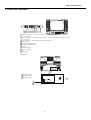
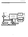
1
HT-3718
COLOUR TELEVISION
Service Manual
Model:
HT-3718
(CYPRUS)
Features
218 programs stored
Auto-correcting black balance
Blue extension, Green improvement
Multi-picture modes
Fast teletext
Audio/video input, S-Video input, SCART terminal
Haier
NO: M-EU-CY-HT-3718-9361
Group
Edition:2003.5.20
CONTENTS
Contents
1
Contents-----------------------------------------------------------------------1
2
Product Code illumination and Series Introduction----------------------2
3
Features----------------------------------------------------------------------------------3
4
Safety Precautions--------------------------------------------------------------------4
5
Warning and Cautions---------------------------------------------------------------5
6
Net dimension--------------------------------------------------------------------------11
7
Parts and Functions------------------------------------------------------------------12
8
Remote Controller Functions-----------------------------------------------------13
9
Program Diagram----------------------------------------------------------------------14
10
Maintenance Service and Trouble shooting----------------------------------15
11
Circuit Diagram-------------------------------------------------------------------------18
12
Circuit Explanation--------------------------------------------------------------------22
13
Adjustment-------------------------------------------------------------------------------27
14
Exploded View--------------------------------------------------------------------------28
15
List of Parts------------------------------------------------------------------------------29
16
Damageable Parts List---------------------------------------------------------------44
17
Information of Resistors and Capacitors--------------------------------------45
1
Product Code illumination and Series Introduction
2.Product Code illumination and Series Introduction
HT-3718
Color television appearance
CRT size(unit:inch)
Philip
haier
2
Functures
1. Features
NO.
MODEL
FUNCTION
ITEM
NO.
FUNCTION
ITEM
HT-3718
1 PICTURE Main IC
2
CRT
3
4
5
6
7
8
9361
Flat square
HT-3718
24 SOFTWARE Digital curtain
25
Slow fading on & off
Color system
PAL
26
Semitransparent menu
Audio system
B/G
27
Non-flashing channel changing
NO.of channels
218
28
ZOOM
OSD language
ENGLISH
29
16:9 mode
30
Games
31
Calendar
Multi-picture modes
AUDIO AV stereo
9
Super woofer
32
Child-lock
10
Surrounding sound
33
Multi-functional lock
11
Treble/bass boost
34
No-picture listening
12
Left/right balancer
35
Background light
13
NICAM
36
Auto-timer on
14
Multi-audio modes
37
CCD
15
Tone adjuster
38
16
MTS/SAP
17
Auto-volume leveling
18
JACK AV input
MODEL
V-CHIP
39 PARAMETER NO. of built-in speakers
40
Audio output power(W)
2
back 1
41
Total power input
70
back 1
42
Voltage range
W
3
19
AV output
20
DVD terminal
43
Power frequency
21
S-video jack
44
Time of sleep timer(MINS)
22
Headphone socket
45
Net weight(KG)
11
23
SCART socket
46
Gross weight(KG)
12
47
Net dimension(MM)
440×355×335
48
Packaged dimension(MM)
475×415×380
49
Quantity for 20' container
50
Quantity for 40' container
51
Quantiry for 40' high container
3
~180-250
V
Hz
50
180
Safety Precautions
4.Safety Precautions
SAFETY PRECAUTIONS
IMPORTANT SAFETY NOTICE
Many electrical identify these parts and mechanical parts in this chassis have special
safety-related characteristics! In the Schematic Diagram and Replacement Parts List.
It is essential that these special safety parts should be replaced with the same components as
recommended in this manual to prevent X-RADIATION, Shock, Fire, or other Hazards.
Do not modify the original design without permission of the manufacturer.
General Guidance
An Isolation Transformer should always be used during the servicing of a receiver whose chassis
is not isolated from the AC power line. Use a transformer of adequate power rating as this protects
the technician from accidents that might result in personal injury caused by electrical shocks.
It will also protect the receiver and it’s components from being damaged by accidental shorts of the
circuitry that might be inadvertently introduced during the service operation.
If any fuse (or Fusible Resistor) in this TV receiver is blown, replace it with a specified one.
When replacing a high wattage resistor (Oxide Metal Film Resistor, over 1W), keep the resistor
10mm away from PCB.
Keep wires away from high voltage or high temperature parts.
Due to the high vacuum and large surface area of the picture tube, extreme care should be taken
in handling the Picture Tube. Do not lift the Picture Tube by its Neck.
X-RAY Radiation
Warning:
The source of X-RAY RADIATION in this TV receiver is the High Voltage Section and the Picture
Tube.
For continued X-RAY RADIATION protection, the replacement tube must be of the same type as
specified in the Replacement Parts List.
Before returning the receiver to the customer,
Always perform an AC leakage current check on the exposed metallic parts of the cabinet, such as
antennas, terminals, etc., to make sure that the set is safe to operate without any danger of
electrical shock.
4
Warning and Cautions
5. Warning and Cautions
Warning and Cautions
1. When you clean the TV set, please pull
out the power plug from AC outlet. Don't
clean the cabinet and the screen with
benzene, petrol and other chemicals.
4. To prevent the TV set from firing and
electric shock, don't
make the TV set rain
or moisture.
2. In order to prolong the using life of the
TV set, please place it on a ventilated
place.
5. Don't open the back cover, otherwise it is
possible to damage the components in the
TV set and harm you.
3. Don't place the
TV set in t h e
sunshine or near
heat source.
6. When the TV set isn't going to be used
for long time or it is in thunder and
lightening, please pull out the plug from AC
outlet and the antenna plug from the cover
of the TV set.
Explanation on the display tube
Generally, it is not needed to clean the tube surface. However, if necessary,its surface can be
cleaned with a dry cotton cloth after cutting off the power.Don't use any cleanser. If using hard
cloth, the tube surface will be damaged.
CAUTION: Before servicing receivers covered by this service manual and its supplements and
addenda, read and follow the SAFETY PRECAUTIONS.
NOTE: If unforeseen circumstances create conflict between the following servicing precautions
5
Warning and Cautions
and any of the safety precautions, always follow the safety precautions. Remember: Safety First.
General Servicing Precautions
5.1 Always unplug the receiver AC power cord from the AC power source before:
a. Removing or reinstalling any component, circuit board module or any other assembly of
the receiver.
b. Disconnecting or reconnecting any receiver electrical plug or other electrical connection.
c. Connecting a test substitute in parallel with an electrolytic capacitor in the receiver.
CAUTION: A wrong substitution part or incorrect installation polarity of electrolytic
capacitors may result in an explosion hazard.
d.
Discharging the picture tube anode.
5.2 Test high voltage only by measuring it with an appropriate high voltage meter or other
voltage-measuring device (DVM, FETVOM, etc.) equipped with a suitable high voltage probe.
Do not test high voltage by “drawing an arc”.
5.3 Discharge the picture tube anode only by (a) first connecting one end of an insulated clip lead
to the degaussing or kine aquadag grounding system shield at the point where the picture tube
socket ground lead is connected, and then (b) touch the other end of the insulated clip lead to
the picture tube anode button, using an insulating handle to avoid personal contact with high
voltage.
5.4
5.5
Do not spray chemicals on or near this receiver or any of its assemblies.
Unless specified otherwise in this service manual, clean electrical contacts only by applying
the following mixture to the contacts with a pipe cleaner, cotton-tipped stick or comparable
nonabrasive applicator; 10% (by volume) Acetone and 90% (by volume) isopropyl alcohol
(90%-99% strength)
CAUTION: This is a flammable mixture.
Unless specified otherwise in this service manual, lubrication of contacts is not required.
5.6
Do not defeat any plug / socket B+ voltage interlocks with which receivers covered by this
service manual might be equipped.
5.7 Do not apply AC power to this instrument and/or any of its electrical assemblies unless all
solid-state device heat sinks are correctly installed.
5.8 Always connect the test receiver ground lead to the receiver chassis ground before
connecting the test receiver positive lead.
Always remove the test receiver ground lead last.
5.9
Use with this receiver only the test fixtures specified in this service manual.
CAUTION: Do not connect the test fixture ground strap to any heat sink in Warning
this receiver.
and Cautions
Electrostatic ally Sensitive (ES) Devices
Some semiconductor (solid state) devices can be damaged easily by static electricity. Such
components are usually called Electrostatic ally Sensitive (ES) Devices. Examples of typical ES
6
Warning and Cautions
devices are integrated circuits and some field effect transistors and semiconductor “chip”
components. The following techniques should be used to help reduce the incidence of component
damage caused by static electricity.
a. Immediately before handling any semiconductor component or semiconductor- equipped
assembly, drain off any electrostatic charge on your body by touching a known earth ground.
Alternatively, obtain and wear a commercially available discharging wrist strap device, which
should be removed to prevent potential shock prior to applying power to the unit under test.
b. After removing an electrical assembly equipped with ES devices, place the assembly on a
conductive surface such as aluminum foil, to prevent electrostatic charge buildup or exposure
of the assembly.
c. Use only a grounded-tip soldering iron to solder or unsolder ES devices.
d.
Use only an anti-static type folder removal device. Some solder removal devices not
classified as “anti-static” can generate electrical charges sufficient to damage ES devices.
e.
Do not use freon-propelled chemicals. These can generate electrical charges sufficient to
damage ES devices.
f.
Do not remove a replacement ES device from its protective package until immediately before
you are ready to install it. (Most replacement ES devices are packaged with leads electrically
shorted together by conductive foam, aluminum foil or comparable conductive material).
g.
Immediately before removing the protective material from the leads of a replacement ES
device, touch the protective material to the chassis or circuit assembly into which the device will
be installed.
CAUTION: Be sure no power is applied to the chassis or circuit, and observe all other safety
precautions.
h.
Minimize bodily motions when handling unpackaged replacement ES devices. (Otherwise
even some normally harmless motions such as mutual brushing of your clothes’ fabric or lifting
of your foot from a carpeted floor might generate static electricity sufficient to damage an ES
device.)
General Soldering Guidelines
a. Use a grounded-tip, low-wattage soldering iron and appropriate tip size and shape that will
maintain tip temperature within the range of 500 oF to 600 oF.
b. Use an appropriate gauge of RMA resin-core solder composed of 60 parts tin/40 parts lead.
c. Keep the soldering iron tip clean and well tinned.
d.
e.
Thoroughly clean the surfaces to be soldered. Use a mall wire bristle (0.5 inch, or 1.25cm)
brush with a metal handle. Do not use freon-propelled spay-on cleaners.
Use the following unsoldering technique
a). Allow the soldering iron tip to reach normal temperature. (500 o F to 600o F)
b). Heating the component lead until the solder melts.
7
Warning and Cautions
a.
draw the melted solder with an anti-static, suction-type solder removal device with solder
braid.
CAUTION: Work quickly to avoid overheating the circuit board printed foil.
f.
Use the following unsoldering technique
A). Allow the soldering iron tip to reach normal temperature. (500 o F to 600o F)
B). First, hold the soldering iron tip and solder the strand against the component lead until the
solder melts.
C). Quickly move the soldering iron tip to the junction of the component lead and the printed
circuit foil, and hold it there only until the solder flows onto and around both the component lead
and the foil.
CAUTION: Work quickly to avoid overheating the circuit board printed foil.
D). Closely inspect the solder area and remove any excess or splashed solder with a small
wire-bristle brush.
Remove /Replacement
Some chassis circuit boards have slotted holes (oblong) through which the IC leads are inserted
and then bent flat against the circuit foil. When holes are of slotted type, the following technique
should be used to remove and replace the IC. When working with boards using the familiar round
hole, use the standard technique as outlined.
Removal
Desolder and straighten each IC lead in one operation by gently prying up on the lead with the
soldering iron tip as the solder melts.
Draw away the melted solder with an anti-static suction-type solder removal device (or with solder
braid) before removing the IC.
Replacement
Carefully insert the replacement IC in the circuit board.
Carefully bend each IC lead against the circuit foil pad and solder it.
Clean the soldered areas with a small wire-bristle brush. (It is not necessary to reapply acrylic
coating to the areas).
“Small-Signal” Discrete Transistor
Removal/Replacement
Remove the defective transistor by clipping its leads as close as possible to the component body.
Bend into a “U” shape the end of each of three leads remaining on the circuit board.
Bend into a “U” shape the replacement transistor leads.
Connect the replacement transistor leads to the corresponding leads extending from the circuit
board and crimp the “U” with long nose pliers to insure metal to metal contact then solder each
connection.
Power Output, Transistor Device
8
Warning and Cautions
Removal/Replacement
Heat and remove all solder from around the transistor leads.
Remove the heat sink mounting screw (if so equipped).
Carefully remove the transistor from the heat sink of the circuit board.
Insert new transistor in the circuit board.
Solder each transistor lead, and clip off excess lead.
Replace heat sink.
Diode Removal/Replacement
Remove defective diode by clipping its leads as close as possible to diode body.
Bend the two remaining leads perpendicularly to the circuit board.
Observing diode polarity, wrap each lead of the new diode round the corresponding lead on the
circuit board.
Securely crimp each connection and solder it.
Inspect (on the circuit board copper side) the solder joints of the two “original” leads. If they are not
shiny, reheat them and if necessary, apply additional solder.
Fuse and Conventional Resistor
Removal/Replacement
a.
Clip each fuse or resistor lead at top of the circuit board hollow stake.
b. Securely crimp the leads of replacement component around notch at stake top.
c. Solder the connections
CAUTION: Maintain original spacing between the replaced component and adjacent
components and the circuit board to prevent excessive component temperatures.
Circuit Board Foil Repair
Excessive heat applied to the copper foil of any printed circuit board will weaken the adhesive that
bonds foil to the circuit board causing the foil to separate from or “lift-off” the board. The following
guidelines and procedures should be followed whenever this condition is encountered.
At IC Connections
To repair a defective copper pattern at IC connections use the following procedure to install a
jumper wire on the copper pattern side of the circuit board. (Use this technique only on IC
connections).
a. Carefully remove the damaged copper pattern with a sharp knife. (Remove only as much
copper as absolutely necessary).
b. Carefully scratch away the solder resist and acrylic coating (if used) from the end of the
remaining copper pattern.
c. Bend a small “U” in one end of a small gauge jumper wire and carefully crimp it around the IC
9
Warning and Cautions
pin. Solder the IC connection.
d. Route the jumper wire along the path of the out-away copper pattern and let it overlap the
previously scraped end of the good copper pattern. Solder the overlapped area and clip off any
excess jumper wire.
At other connections
Use the following technique to repair the defective copper pattern at connections other than IC
Pins. This technique involves the installation of a jumper wire on the component side of the circuit
board.
a. Remove the defective copper pattern with a sharp knife.
Remove at least 1/4 inch of copper, to insure that a hazardous condition will not exist if the
jumper wire opens.
b. Trace along the copper pattern from both sides of the pattern break and locate the nearest
component that is directly connected to the affected copper pattern.
c. Connect insulated 20-gauge jumper wire from the lead of the nearest component on one side of
the pattern break to the lead of the nearest component on the other side.
Carefully crimp and solder the connections.
CAUTION: Be sure the insulated jumper wire is dressed so that it does not touch components or
sharp edges.
10
Net dimension
6. Net dimension
Top-view
Side view
Front view
HT-3718
11
Parts and Functions
7. Parts and Functions
FUNCTION BUTTONS AND EXTERNAL SOCKETS
1.Front Panel
Remote sensor:let The remote controller aim here the set can receive remote
control signal.
Power switch:Press the button to turn on the TV set . press the button again to turn
off the TV set.
Power indicator: the indicator lights when power on .
Menu button
program up/down button
Volume up/down button
TV/AV
Audio (R) input
Audio (L) input
Video input
2.Rear Panel
S-VIDEO input
SCART socket
Antenna input
12
Remote Controller Functions
8. Remote Controller Functions
Remote Controller
R EM O TE C O N TR O LLER BO A R D
M A RK
FU N C T IO N D E SC R IPTIO N
Program scan
Standby
SW A P
M ute
1
2
3
TV /AV
-V O L +
-C H +
P.P
PIC TU R E
?
TV /V ID E O SE LE C TIO N
V O L U M E C O N TR O L
C H A N N E L N U M B E R U P/D O W N
PIC TU R E M E N U
SO U N D SO U N D M E N U
TIM E M E N U
TIM E
FUNCTION FU N C TIO N M EN U
O N E D IG IT SE LE C TIO N
0-9
-/-M E N U M E N U D ISPL A Y
EX IT M EN U D ISPL A Y
A 2/N IC A M /M O N O SO U N D SEL EC T IO N
PIC TU R E M O D E SE LE C TIO N
N O U SE D
T U N E M EN U SEL E C T IO N
T E L E T E X T S U B T IT L E
TV /T EL ETE X T E N TE R IN G /E X ITIN G
TO R EV EA L C O N C E A LE D TEL ET EX T
TE LE TE X T ZO O M
T E L E T E X T PA G E H O L D
T E L E T E X T /T V M IX M O D E
TV /T EL ETE X T A LTER A TIO N
EA ST/W E ST
N O TE
T he function of selecting m enu button on the rem ote controller is
the sam e as thatof program up/dow n button on the T V set.
T he fuction of identifying m enu button on the rem ote controller
is the sam e as thatof volum e up/dow n button on the TV set.
13
Program Diagram
9. Program Diagram
Insert the power plug into the power line socket and insert the antenna plug into the antenna
socket on the rear panel. Press down the power switch of the TV set. The red indicator light goes
on. If no picture appears, press the button
on the remote controller. Follow the steps below.
A
Program preset
1. Auto searching and storing program
Press MENU button on the remote controller then use the “CH+/CH-“ key to call up the “tune
program” menu on the screen. Then Press the menu” VOL+/VOL- “ item to adjust. it.Use the
“CH+/CH- ” key to select the bar “auto search program” then press the “VOL+/VOL-” to make
sure. If you want to stop ,press the key “ MENU ”.
2. Manual search and fine tune
Press MENU button then use the “CH+/CH-“ key to call up the “tune program” menu on the
screen. Then Press the menu” VOL+/VOL- “ item to adjust. it.Use the “CH+/CH-” key to select
the bar “Manual search program” then press the “VOL+/VOL-” to make sure.
3.Deleting channel number
Press Program up/down buttons to select a channel to skip. Press MENU to call Menu. then
use the “CH+/CH- “ key to call up the “tune program” menu on the screen. Then Press the
menu” VOL+/VOL- “ item to adjust. it.Use the “CH+/CH-” key to select the bar “Cannal
number” then press the “VOL+/VOL-” to make sure. Enter the number that you do not want to
see .Then Then select “SKIP” and select SKIP to ON. Now the program number is deleted.
Repeat the above steps and select SKIP to OFF, the deleted program number can be resumed.
B
Volume tuning
Press VOLUME buttons
C
VOL+ to increase and
VOL- to decrease the volume.
Personal preference settings
Picture modes
Press SELC PICTURE repeatedly to change among MEMORY 1, MEMORY2,MEMORY3,to chang
the Picture Mode.
14
Maintenance Service and Trouble shooting
10. Maintenance Service and Trouble shooting
a.Factory adjustment information
Operation method: after the appliance is switched on, press MUTE CALL -/--
CALL
MUTE
Button in turn and enter service mode.
Press PRO- and PRO+ buttons to select items for adjustment.
Press VOL- and VOL+ buttons to adjust selected items.
Press the POWER button to switch off the appliance and go back to the normal state.
Maintenance menu (Table 8)
Item
5PAR
5BOW
5HSH
5EWW
5EWP
5UCR
5LCR
5EWT
5VSL
5VAM
5SCL
5VSH
5VOF
HOF
VX
6PAR
6BOW
6HSH
6EWW
6EWP
6UCR
6LCR
6EWT
6VSL
6VAM
6SCL
6VSH
6VOF
HOF
VX
RED
GRN
Specifications
Horizontal parabola
Horizontal Bow
Horizontal shife
EW width
EW parabola
EW upper corner parabola
EW lower corner parabola
EW trapezium
Vertical slope
Vertical amplitude
S-Correction
Vertical Shift
OSD Vertical Offset
OSD Horizontall Offset
Vertical Zoom
Horizontal parabola
Horizontal Bow
Horizontal shife
EW width
EW parabola
EW upper corner parabola
EW lower corner parabola
EW trapezium
Vertical slope
Vertical amplitude
S-Correction
Vertical Shift
OSD Vertical Offset
OSD Horizontall Offset
Vertical Zoom
Black level offset R
Black level offset G
Default Value
40
Variable
Mark
*
*
*
*
*
42
55
21
28
40
40
32
32
15
*
*
Maintenance Service and Trouble shooting
Item
WPR
WPG
WPB
YDFP
YDFN
YDAV
TOP
VOL
9874
AVLT
9860
IFFS
HDOL
AGC
VF2B
0CON
0BRI
0COL
0SHP
1CON
1BRI
1COL
1SHP
2CON
2BRI
2COL
2SHP
3CON
3BRI
3COL
3SHP
OP1
OP2
OP3
OP4
OP5
OP6
OP7
Specifications
White point R
White point G
White point B
Y-Delay for PAL
Y-Delay for NTSC
Y-Delay for AV
AGC Take-Over point
Volume
Output Gain of TDA9874A
TDA9874A AVL decay time
Sub volume of TDA9860/59
Vision IF
Cathode drive level
IF AGC speed
VG2 Brightness
Listen:Contrast
Listen:Brightness
Listen:Color
Listen:Sharpness
Soft: Contrast
Soft: Brightness
Soft: Color
Soft: Sharpness
Standard: Contrast
Standard: Brightness
Standard: Color
Standard: Sharpness
Dynamic: Contrast
Dynamic: Brightness
Dynamic: Color
Dynamic: Sharpness
Option 1
Option2
Option3
Option4
Option5
Option6
Option7
Default Value
31
26
31
7
32
44
26
1
69
2
5
1
50
0
0
50
50
45
45
50
50
70
50
60
50
80
50
70
50
177
127
255
75
183
89
1
You can change the DATA with “*” mark when necessary.
16
Variable
Mark
*
*
*
*
*
*
*
Maintenance Service and Trouble shooting
No light and sound
Check to see if
Fuse3 is normal
Abnormal
Normal
Check to see 110V 180V
etc. voltage is normal
Check VD503-VD,
506,C511, N501, etc.
Normal
Abnormal
Check to see if the
collector voltage of
VD512is 24V
Normal
Check to see
if , 8v,
5v is normal
Normal
Check
N507,N508
Test to see all terminal
Resistance of load
Is normal
Abnormal Normal
Check the control
voltage of VD512
or CPU power
Abnormal
Check switch
power unit
Abnormal
Check to see if
rectifying tube
is normal
Normal
Change
rectifying tube
The failure of
horizontal unit or
N201
17
Abnormal
Check the
Loader
Circuit Diagram
11. Circuit Diagram
1
2
3
4
5
C406
1uF/ 16V
L?
VI DEO i n
Text
ALi n
ARi n
Ri n
VIDEO out
Bi n
ALout
XS3 0 6
ARout
R303
100
10k
R302
100
9
R324
4. 7k
N3 0 1
1
2
3
4
5
6
7
(R)
8
9
N3 0 2
10
1
2
3
LA4 2 85 /8 7
4
C303
0. 015
C311
10/16V
10/16V
LA4 28 5 /8 7
5
6
7
8
47K
47K
C402
10uF/ 16V
9
R703
1. 8K
C302
0. 01
8W/8OHM
C310
V402
C1815
R425
470
9
10
11
12
13
14
0
VD310
C325
0. 01
0
1
0
1
R2
4
5
5
1
6
2
7
3
C319
16V/100u
C412
22nF
VD331
1N4148
R406
47K
6. 0
1
C704
4. 7u
2
DZ701
MTZJ9. 1B
R705
2. 4
R710
100
R726
68
R712
100
116
R711
100
114
111
VD701
ERC24- 06
3
PROBE3
PROBE2
8
CN702
CN701
C702
PROBE1
C498
22nF
L2
3. 0
DZ704
DZ703
DZ702
MTZJ9. 1B MTZJ9. 1B MTZJ9. 1B
178. 5
R330
10k
R314
10k
8
7
6
5
4
3
1
2
+
C411
22nF
3
4
9
C499
22nF
V332
2SC1815
R311
1k
3
D
R704
10M
8
V2
V331
2SA1015
V333
2SC1815
+ C415
22uF/ 16V
C409
1uF/ 16V
3. 0
6 VDD 7
R419
10
2
+12V
8V
AV-IN
2
!
CRT
5
N401
HEF4053
1
R709
100
C316 C314
0. 01u 16V/100u
R332
10k
1
3. 0
R708
100
VD311
1N4148
C318
16V/100u
1N4148
XS3 0 2
R707
100
4
1
C315
50V/2. 2u
R312
10k
C312
0. 01u
N701
TDA6107Q
CN703
C327
0. 1u
VD312
1N4148
R702
1. 8K
XS3 0 2 8W/8OHM
V3
15
4. 7k
22
C709
391
V2
16
R327
VD321
1N4148
C324
100/16V
1N4148
C329
2. 2/50V
C420
10uF
C321
25V/470u
C708
391
3 GND
C323
100/16V
C707
391
C317
0. 1u
22
2
VD320
R701
1. 8K
R317
R304
+8V
+8V
C403
R310
680
C321
10/16V
R320
680
22nF
HV
V1
R401 82
R322
10k
FO
C306
25V/1000u
10
1
R417
10
R321
4. 7k
SC
GT702 1P
C313
1
R409
2
R408
CN000
R411 82
C703
103
GT701 1P
C307
0. 01u
(L)
0. 015
+
D
R410 82
R412 82
R418
68
3
R412 82
C404
22nF
+5V
12
11
MAIN BOARD
25V/470u
100K
10
10/16V
C328
R328
R426
8
20V
C330
0. 01
+
R421
470
7
C331
R331 4. 7k
C326 0. 01
C407
1uF/ 16V
+
Gi n
2L
R329 4. 7k
V401
C1815
C405
10uF/ 16V
1R
+
R420 100K
SOCKET- 21
6
222
C706
10u
R727
R499
47K
VD702
ERB4304
VD703
ERB4304
VD704
ERB4304
33K
C401
470uF
Band1
10K
R198
2
St andby
SCL
SDA
1
4
t uni ng
Syst em
Key
3
6
5
7
VOL1
VOL2
Vss C/ P
8
9
10
Band1
11
12
Band2
Vp2
SECPLL
VssA
13
14
15
DECDI G
16
PH2LF
PH1LF
17
18
19
DECBG
AVL/ EWD
VDRB
Gnd3
21
20
22
VDRA
I F1
I F2
23
25
24
VSC
I REF
AUDEEM/ SI F1
Tuner AGC
26
27
28
30
29
Gnd2
R248
5. 6K
R276
100
C270
33pF
Vi deo/ SVHS- Y
RN08
10K
2. 7K RN09
1
VI F1
2
VI F2
5
3
4
TOP
CCS
MUTE
7
6
Tpl l
n. c.
Vo- CVBS
8
9
10
Caf
Vo- AF
20
19
Vp
Cagc
GND
VCO1
VCO2
18
17
16
AFC
Vo( vi d)
Vi ( vi d)
15
14
TAGC
Vi - I C
3
2
VI FB
VOA
VFB
Gnd
VOB
Vp
I-
I+
Vguar d
8
7
6
5
4
3
2
1
9
CN25
2. 2uF
0. 47uF
1
1
CN21
I Ri n
AV2
63
62
64
1
C918
390n/ 250V
V957
D2012
VD950
1N4148
R916
100 2W
R801
33K
C917
+ C921
1uF/ 160V
+
+
3
12
9
13
Focus
C916
100uF/ 63V
220uF/ 25V
G2
1
R922
1K
7
2
L905
6. 8mH
C920
100nF
C909
10uF/ 160V
+
+
R911
2. 2/ 0. 5W
C912
470pF/ 500V
VD911
1N4148
A
CON4
VD907
BYD33J
7
R912
6. 8
VD912
BY228
C915
4.7uF/ 250V
R920
220K
X903
4
3
2
1
L902
600uH
C958
0. 47uF
0. 033uF/ 630V
C910
1000pF/ 500V
100
!
VD501
ER
Z14V471K
4A/ 250V
1
2
3
4
5
6
7
19
8
42
R905
V901
BF422L
41
C535
470uF/ 25V
R910
82
2. 2K
MONO I N
4
VD906
BYD33G
C906
C913
EXT I R
R908
+16V
H
X902
CON5
FBT2
5n6/ 2KV
1
C515
100uF/ 16V
V902
BU2508DX
40
R501
0.5W220K
+
+
T901
H- DRI VER
EXTI L
Gnd
7805
11
5
Gnd
+110V
C902
4700pF/ 500V
2
!
F501
!
C533
AC400V2200p
!
R902
100
I n Out
V508
2SC536
XP501
+
39
+8V
VD516
BYV95A
V956
2PA1015
270
C901
47uF/ 50V
C534
100uF/ 16V
N506
P1
R529
0.5W8. 2M
+
VD905
BYV95B
14V
C926
330n/ 500V
R956
5. 6/ 1W
+24V
R907
2
Vssd3
R528
0.5W8. 2M
C513
47u
+5V
Vr ef 2
!
!
Gnd
C547
100uF/ 16V
R546
10K
R915
1K 0. 5W
C908
8n2/ 2KV
I n Out
+
R503
1. 5K
C532
470pF/ 500V
L901
H- LI NE
+
R950
5. 6K
C956
470uF/ 6. 3V
3
11
VD520
ERB4304
C538
100uF/ 16V
38
R537
2. 2K
+
Vddd3
V509
2SB892
DZ595
BZX79C5V1
N507
7805
P2
S501
KDC-A04-S
10
C537
470uF/ 35V
43V
R806
2. 2/ 1W
R951
R952
18K
R979
1K
4
!
R517
600
VD596
I N4148
+
5
4
3
2
1
10
EHT
R955
2. 7K
56K
PI NC
+
R978
39K
C957
0. 1uF
430
+
C537
470uF/ 25V
RP951
47K
37
VD520A
B1206
473
C514
C953
0. 22uF
+5V- 1
RP950
10K
H. WI DTH
V952
C1815
5
735504C
0.1u/ 250VAC
R971
1. 5K
R539
C536
470pF/ 500V
16
36
C598
392
R511A
33K
R959
2. 2K
+ C806
22uF/ 63V
R981
6. 8K
SYSCLK
R515A
33K
R578
470
2
+
R977
220K
R972
10K
10uF/ 50V
C955
0. 1uF
R970
270
R980
6. 8K
C951
OUT M
10
C501
C950
10uF/ 16V
1
R598
L501
Gnd
C952
100uF/ 16V
R927
2. 2
33/ 0. 5W
R976
6. 8K
6
220u/ 400V
35
AC400V
C502
R536
1/ 1W
R969
820
R999
39K
Gnd
0.1u/ 250VAC
SCK
14
V950
2PA1015
R975
100K
L801
2uH
V
!
8
V951
C1815
R968 1. 5K
DZ506
BZX79C2V7
7
VD515
BYD33D
R967
1K
st andby
C1815
15
Vssa4
SYNC
5
7
2
VCC
3
R964
470K
+3. 3V
R530
10K
V508
9
C531
222
34
L01
1 F/ B
C507
!
L802
R807
+
V540
C1815
C526
100uF/ 35V
WS
C
508~C511
1KV 1000P
R500A
470K
VFB
R529
1. 5K
+
C525
470pF/ 500V
SDO
R502
7W1. 5
DI ODE
47nF/ 100V
6
R541
1K
V541
C1815
R535
2.2/ 0. 33W
12
OUT R
!
D?
1. 5
270/ 2W
+24V
R540
1K
+24V
13
OUT L
3
L504
8
N501
4
33
R500B
470K
5W 270
!
3. 3
C809
R810
R809
3.3 0. 5W
R806
R966
10
VD512
BYD33D
LF-U16-001
SDA
2
1
A
R811
3. 3 0. 5W
R538
56/ 2W
T501
R505
1
R813
2. 7K
2uH
C521
470pF/ 500V
!
L502
Vdda1
C522
100uF/ 35V
9
!
3
100
R576
15K
R521
2. 2K
+
CN31
0. 47uF
CN30
0. 47uF
ZD802
BZX79C12V
C808
0. 01uF
C880
220nF
12. 5V
R581
22K
RN23
100
T902
VD503~VD506
RM11C
RT501
MZ73-18
1
C803
0. 01uF
+
KSC815
R573
2. 49K
VD511
BYD33D
10K
XS502
C805
220uF/ 25V
32
RLP1
LK1aF- 12V
R803
2. 2K
C802
2. 2nF
C905
220pF/ 500V
V571
1N4148
N571
KA431
V601
2SC536
C959
4. 7uF
10K
SCL
VD572
Vssa1
R579
R577
39K
10
127K
R591
1. 5K C571
104
R572
1K
R812
5. 6K
31
220V
C807
220nF
B
RN25
R804
680K
2. 2nF
CN17
LN05
1uH
RN22
100
CN29
0. 47uF
RN20
C801
BZX79C15V
R901
3. 9K
Vdda3
220V
1N4148
R926
4. 7K
BZX79C8V2
8. 2K
2. 2K
0. 01uF
CN18
47uF
Vssd1
DZ900
110V
R571
CN19
0. 01uF
11
30
!
ABL
12
29
VD507
PCT817C
N801
TDA8357
R802
CN22
0. 47uF
VSSa3
C602
16V 100uF
DZ901
R917
680
Gnd
!
XP502
*
1K
V Drv +
I n Out
V602
2SC536
V Drv _
R918
VD908
1N4148
CN23
0. 47uF
Vddd1
Vssd2
28
27
26
25
24
RN19
120K
220V
R603
22K
+
R932
STANDBY
22K
6. 8
0. 022
NN02
CN28
1uF
CN26
0. 1uF
VDr v+
+5V
VD605
RN15
TD
A9874APS
CRESET
SI F2
TEST1
Vdec
23
22
R925
5. 1K*
3. 3K
Cb
Lr ef
Y
+8V
Vssa2
R296
1K
XS5
R931
C925
0. 22uF
Cr
SW
ADDR2
C262
4. 7uF
VD297
1N4148
V299
2SC1815
VD910
1N4148
SI F1
+5V R297
10K
XS001
C291
4. 7uF
VD299
1N4148
VD298
1N4148
Vr ef 1
L271
10uH
+3. 3V
10K
R213
3. 3K
R299
3. 3K
13
R212
3. 3K
14
10uF
C275
47uF
+8V
Z255
XT4. 5
St andby
R604
10K
CN10
LN03
1uH
C272
TP2
Audi o 2
1N4148
61
AV1
C269
33pF
100uF
L260
10uH
NI CAM DATE OUT
1N4148
L270
10uH
C268
VD201
AV1
VddP
Reset
XTALout
59
60
XTALi n
OscGnd
57
58
VddC
56
VpE
VddA
55
54
Bout
Gout
R275
100
VD202
1N4148
R282
47
22nF
15
VD203
C271
PCLK
C924
0. 22uF
C266
1000pF
53
52
Rout
Bl anki ng
51
50
BCLi n
B2/ Ui n
G2/ Yi n
48
49
R270
2. 2K
R930
1. 5K
C260
0. 1uF
R249
1. 2K
L201
10uH
R267
27K
47
46
R2/ Vi n
I NSSW2
AUDOUT/ AMOUT
C248
1000pF
45
44
CHROMA
42
40
43
CVBS/ Y
Gnd1
CVBSI NT
Vp1
I FVO/ SVO
39
38
PLLI F
37
36
41
C245
1. 0uF
Z202
12MHz
TP1
R253
V256
2SC1815
C242
1. 0uF
C267
22nF
17
C229
1nF
C247
100uF
C241
100nF
R272
100
ADDR1
L252
6. 8uH
470
C246
22nF
Video Out
+5V
RN12
coi l
RN16
RN18
10
ZN03
24. 576MHz
16
+8V
R247
390
VD001
C600
50V 470uF
ZN02
0. 022uF
Gnd
18
R262
27K
R257
V255
2SC1815
R258
4K7
N602
7805
2. 2uF
CN11
10uF
CN12
CN16
100pF
IR
XTALO
Z252
XT5. 5
EHTO
AUDEXT/ QSSO
FBI SO
33
R251
180
R266
100K
SLP-177B
TP1
DB- 1. 3- 08
LN02
1. 8uH
SA
St andby
N201
TDA9361
CP101
19
R000
180
C240
4. 7uF
R245
1. 8K
+8V
R009
R261
100
1. 8K
Z251
XT6. 0
R259
2. 2K
+3. 3V
R255
100
35
H out
150
B
EM01Z
VD601 VD604
CN15
8. 2pF
RN17
1
R268
1. 5K
3. 3K
R250
2SC1815
V250
R252
34
L250
8. 2uH
Z250
XT6. 5
R260
39
R002
470
SW002
R211
3. 3K
10nF
SVHS- C
2SC1815
V252
L01
TV/AV
R216
3. 3K
TEST2
SW003
R005
620
R215
3. 3K
XTAL1
R006
1k
R217
1K
20
MENU
SW004
R219
1. 2K
21
CH-
R222
1. 2K
C
C132
R256
220
R007
1. 2K
C218
220nF
+8V
SW007
SW005
C221
220nF
+5A
C250
47uF
SW006
CN09
C222
2. 2nF
22nF
38M
R265
47
CH+
RN06
2. 7K
C225
K7266
V102
2SC1815
56K
R115
82K
R008
1. 8K
C207
56PF
6
VD101
BAT81
DECSDEM/ SI F2
Z201
R118
3. 3K
R116
R111
22
SNDPLL/ SI FAGC
C112
R107
2. 2K
31
32
R117
2. 2K
0. 01uF
V101
2SC2216
VOL-
R220
3. 3K
+
R119
4K7
L102
1uH
0. 01uF
VOL+
R221
27K
NN01
ZN01
k9261
1nF
0. 022uF
C230
3. 3uF
R239
39K
C232
100nF
C208
56PF
C209
R225
27K
390
1
10
R110
180
AVL/ REFO
+8V
01uF
R112 0.
C115
R108
C199
4. 7K
0. 01uF
C110
IF
C235
6800pF
R208
100
2K
C109
0. 01u
C108
16V/100u
C236
10uF
R242
3. 9K
Band2
L101
10uH
10K
+5V
BM
C237
1. 2nF
SDA
+5V
22nF
C226
2. 2uF
C239
1. 0uF
GND
VN01
BF370
+
H/L
C106
10uF
R235
15k
SCL
+
C105
10uF
C231
22nF
C238
330pF
4K7
+8V
A2
CN03
CN20 2. 2uF
R199
U/V
R440
Video Out
100uF
C215
C219
4. 7nF
R226
5. 6K
22nF
2. 2uF
CN05
0. 022uF
RN05
150K
0. 01uF
R207
100
RN10
13
V403
C1815
Tuni ng
10K
C228
1nF
TEST
CN07
12
R201
2SC1815
V103
C227
1nF
R227
5. 6K
A1
0. 1uF
CN06
CN08
SB
+
10K
C220
1uF
VCC
C206
C210
10uF
R230
4. 7K
A0
+
C201
100nF
R202
R237
100
R231
4. 7K
R210
4K7
+
TDA9801
LAN
C103
100nF
4K7
R238
100
R218
47
RN07
10
R209
100
NC
GND
NC
NC
R. OUT
L. OUT
C102
0. 01uF
TU
R241
680
R228
3. 3K
N2 0 2
AT2 4 C04 /0 8
SA:
1
2
3
4
5
6
C
R236
100K
R441
4K7
SYS
C216
10uF
C212
AGC
6. 8K
R102
L205
10uH
+8V
VOL1
R232
3. 3K
+8V
R240
10K
R205
12k
R101
C101
4. 7uF
+5A
VOL2
Band1
Band2
+5V
+110V
U2 0 1
TDQ AGC
VOL2
V Dr v-
11
V Dr v+
AGC
R206
10K/ 3W
C205
10uF/ 50V
VOL1
SW
B
100uF CN35
G
SYS
0. 022uF
R
VI DEO/ Y
+5V
DZ203
UPC574
Tuni ng
AV1
SYS
R416
82
+
SVHS- C
R415
82
IF IN
NC
+5V(+8V)
GND
SCL
SDA
FM IN
SVHS- C
CN32
SB:
0
1
2
3
4
5
6
SVHS- Y
X105
S- VHS
9
10
11
12
Circuit Block Diagram
11.2 Circuit Block Diagram
Antenna
Picture/Sound IF Amplifier,
Tuner
Sound Power
Amplifier
Video and audio signal
SAW
Processing,
RGB Output Circuits
and H &V Sync pulse
segregation
CRT
Horizontal Scan
Output
I2C BUS
Vertical Scan
Output
Main Processor
ROM
Audio/Video In/Out
Infrared Receiver
Remote Controller
20
Circuit Diagram
11.3 PCB
21
Circuit Explanation
12. Circuit Explanation
A1.HT-3718 color TV set composed of the following sections
(1) Small signal processing: super monolithic integrated circuits N201(TDA9361). and
memory N901 (AT24C08).
(2) Sound power amplifying: integrated circuits N301,N302 ( LA4285).
(3) Horizontal and Vertical scan output circuits: Vertical output integrated circuits
N801(TDA8357), Horizontal output transistor V902 (2SD1651), Horizontal flying back
transformer T902 (JF0501-19930).
(4) Switch power supply: switch transformer T501 (BCK-08A5), power transistor N501
(5Q0765).
(5) AV switch integrated circuits N401(HEF4053).
A2.
Main integrated circuits:
(1) TDA9361
(2) LA4285
(3) TDA8357
A3.
Microprocessor
Picture IF/sound IF/video processing/H and V
Scan/color decoding
Vertical output integrated circuits
Sound power amplifying integrated circuits
Electrical circuit analysis
1) Microprocessor and Small signal processing: super monolithic integrated circuits
TDA9361
TDA9361 is super large integrated circuit decoder, containing intermediate image
amplifying, teletext processing, intermediate sound amplifying, horizontal and vertical scan,
small signal processing, color decoding, hi-pressure tracing and over-load protection, I2C
bus control.
Information introducing functions and testing data for maintenance is listed in Table 1.
Table 1
Step
1.
2.
3.
4.
5.
6.
7.
8.
9.
Working
Voltage
V
0.1
3.5
3.2
0.4
3.2
3.1
4.42
4.42
0
Function
STANDBY
SCL
SDA
Tuning
SYSTEM
KEY
VOL1
VOL2
VSS C/P
22
Ground Resistance(R)
Positive
Negative
12.58K
12.62K
12.62K
0.5M
11.7K
33K
10.6K
10.6K
0
12.87K
12.9K
12.9K
257K
11.9K
30K
10.9K
10.9K
0
Circuit Explanation
Step
Working
Voltage
V
0
6.38
0
2.3
7.7
5.0
2.9
3.9
0
4.0
0
0.7
0.7
1.9
1.9
3.84
3.8
0.1
2.9
2.4
0
2.3
0.2
0.6
0.4
3.6
1.1
1.4
2.6
7.7
3.44
0
3.8
1.5
3.4
3.1
2.6
2.6
2.6
2.3
5.1
3.3
3.3
3.3
3.1
0
Function
10.
11.
12.
13.
14.
15.
16.
17.
18.
19.
20.
21.
22.
23.
24.
25.
26.
27.
28.
29.
30.
31.
32.
33.
34.
35.
36.
37.
38.
39.
40.
41.
42.
43.
44.
45.
46.
47.
48.
49.
50.
51.
52.
53.
54.
55.
BAND1
BAND2
VSSA
SEC.PLL
VP2
DECD/G
PH2.LF
PH1.LF
GND3
DEC.BG
AVL/EWD
V.DRB
V.DRA
IF.IN1
IF.IN2
I.REF
V.S.C.
TUNER.AGC
AU.DEEM/SIF1
DECS.DEM/SIF2
GND2
SND.PLL/SIF AGC
AVL/REFO
H.OUT
F.B.L.SO
AUO.EXT
EHTO
PLL.IF
IF.VO/SVO
VP1
CVBS.INT
GND1
CVBS/Y
CHROMA
AUD.OUT/AMOUT
INSS.W2 BL
R2/V.IN
G2/Y.IN
B2/U.IN
BCL.IN
BLK.IN
R.OUT
G.OUT
B.OUT
VDD.A
VPE
23
Ground Resistance(R)
Negative
Positive
11.9K
3.0K
0
6.86M
0.77K
30K
1.33M
6.8M
0
37.3K
6.9M
1.9K
1.9K
35.3K
35.3K
39.1K
6.72M
13K
1.44M
6.92M
0
1.38M
6.82M
2.56K
30.2K
6.92M
12K
6.76M
0.98M
0.77K
6.76M
0
4.56M
80.8K
1.2M
0.72K
1.88M
1.86M
1.85M
321.5K
23.2K
5.6K
5.5K
5.5K
30K
0
10K
3.0K
0
4.4M
0.75K
29.9K
0.45M
4.2M
0
37.2K
4.6M
1.9K
1.9K
35.6K
35.6K
39K
4.96M
10.5K
2.04M
4.64M
0
0.42M
3.96M
2.54K
30K
4.92M
12K
4.93M
0.38M
0.75K
4.2M
0
384K
80.8K
1.66M
0.71K
2.12M
2.12M
2.16M
4.68M
23.1K
5.54K
5.48K
5.5K
26.2K
0
Circuit Explanation
Circuit Explanation
Function
Working
Voltage
V
3.1
0
1.5
1.6
0
3.1
4.8
4.8
4.9
Step
56.
57.
58.
59.
60.
61.
62.
63.
64.
VDD.C
OSC.GND
XTAL.IN
XTAL.OUT
RESET
VDDP
AV1
AV2
IRin
Ground Resistance(R)
Negative
Positive
30K
15.4
1.17M
0.74M
0
30K
12.8K
12.8K
36.9K
26.2K
14
262K
227K
0
26.2K
12.9K
12.9K
34.6K
2).
Analysis of common path circuits
High frequency television signals, received via an antenna (or transmitted through a cable
TV system) to the input terminal of the high frequency tuner U101, are processed for tuning
and high frequency amplifying and mixing, then a 38.9MHz image intermediate frequency and
31.5MHZ sound intermediate frequency signal will be released at the IF terminal of TU101 to b
of the transistor V101 , where signals are amplified to compensate for the insertion losses of
the sound surface wave filter. Single or dual-ended input is used for the sound surface wave
filters Z101 of this appliance according to system properties. Intermediate frequency signals
will be transmitted to (23) and (24) of N201(TDA9361). High frequency amplify AGC output
from (27) of N201 controls the gain of the high frequency tuner.
3).
Analysis of signal trap switch circuit
Color video signal output from (38) of N201 through V250 to Z250-Z252 and Z255.All television signal
is selected by V255 and V256 then pass.V255 and V256 are band-pass transistors, take part in switch at
the location. The pin 5 of N201 is high level (sound frequency isn’t 4.5MHZ ), V256 conducts the signal
pass through Z250-Z252 channel. When pin 6 of N201 is low level. V256 cut off and V255 conducts,
the signal pass through Z255 channel. After the all television signal pass through the traps, video signal
is gained, then after it pass through R260, R261,C242,N201(pin 40), V403 , it is used in AV output.
Video signal of AV and Y signal of s-terminal pass through N401 (HEF4053BP) are selected and go into
pin 42 of N201; C signal of s-terminal go into pin 43 of N201.
R,G , B signal of RGB component respectively pass C291, C260, C261 to couple, go to pin 46, pin 47,
pin 48 of N201.
4). Analysis of sound power amplifying circuits
Sound power amplifying circuits are composed of integrated circuits N301 (LA4285/87) and
N302 (LA4285/87) peripheral components. LA4285/87 is an integrated electrical circuit .
Information introducing functions and testing data for LA4285/87 maintenance is listed in Table
24
Circuit Explanation
Table 4
No.
1
2
3
4
5
6
7
8
9
10
Working
Voltage
V
6.27
0
5.51
1.21
4.19
9.21
9.19
0
9.25
20
Function
INT
GND
EXT
SW
VOL
FL1
NFB
GND
OUT
VCC
Ground Resistance(R)
Positive
Negative
54.4K
2.6
54.1K
86.2K
20K
13.5K
32.5K
3
44K
0.4M
53.3K
0
53.1K
86.6K
20.5K
13.3K
32.3K
1.5
42K
0.4M
5). Analysis of horizontal sync and horizontal scan output circuits
As the horizontal oscillation circuit is installed inside N201 (TDA9361), . Some brightness
signals including compound sync signals are transmitted to the internal sync segregation
circuits, where horizontal sync and vertical sync pulses are segregated. C219(472) ,
R235(15K)
C220(1u) are connected to N201 (17) are phase-lock loop filters. Horizontal
pumping signals are transmitted from (33) of N201 to horizontal promotion transistor V901
(2SD2383), and then drive the H-DRIVE transformer. After being amplified through it switches
power transistor to control the horizontal scan of the electronic-beam. C918 is a horizontal S
correction capacitor and L901 is for horizontal linear inductor. T902 is a horizontal output
transformer.VD908,R932,R267,R266,C229 are ABL circuits. R930,R931,VD910,C925 consist
of beam-current limit circuit. H-return-trace pulse from pin 4 and pin 3 of horizontal output
transformer T444 via rectification, filt and obtain DC voltage +16.5V and +46V and feedback
to pin 3 and pin6 of N801 for forward and return trace Vertical IC to supply power.
Pin 8 of N801 put out heater voltage 6.3V, pin 6 of N801 supply sync signal for N201 ; pin 9
of N801 put out Horizontal return trace pulse, via rectification, filt and obtain DC +180V for
video amplifying circuit supply power.
6). Analysis of video amplifying circuits
The video amplifying circuits are comprised of N701 (TDA6107Q) and peripheral components.
B, G and R signals output from N201 (51), (52) and (53) go into pin2, pin3, pin1 of N701,
TDA6107Q has 3 video power transistor are available for amplifying the input R, G, B and they
go into cathode of CRT. Pin 5 of N501 is used to check black balance output and checking
signal go into pin 50 of N201 and adjust picture black balance. White balance adjustment is
completed through control of an I2C serial bus control system. Information introducing functions
and testing data for TDA6107Q maintenance is listed in Table 6.
25
Circuit Explanation
Table 6
Step
1
2
3
4
5
6
7
8
9
7).
Working
Voltage
V
2.9
2.9
2.9
0
3.8
164.9
114.5
114.2
113.4
FUNCTION
B IN
R IN
G IN
GND
F/B
VCC
G OUT
R OUT
B OUT
Ground Resistance (R)
Positive
Negative
5.44K
5.44K
5.38K
0
13.24K
34K
2.1M
1.8M
2.1M
5.43K
5.45K
5.39K
0
13.3K
30K
3.24M
3.22M
3.22M
Analysis of switching mode power circuits
The installed switching mode power source is a typical autonomous pulse switch power source.
The circuits are comprised of IC N501, switching mode transformer T501, bridge-rectifier
components. When the switch is set to on, the pulse voltage of the 220V voltage rectified by
VD503-VD506 rectifier is filtered by the capacitor C511 (1500uF) to obtain +300V direct current,
which is added through (3)-(7) of the switching mode transformer T501 to the pin1 of IC N501.
When the appliance is first switched on. The coupler VD507 (PC817B inlet) functions to control
voltage, and the voltage tolerance information from T501 are transmitted to pin4 of N501 via
VD507 to control the switch velocity and hold the output voltage normal.
The pulse voltage output from the secondary (12) of the switching mode transformer T501,
rectified and filtered by V511(RU3A) and C522 is +110V direct current voltage which is
horizontal voltage. The pulse voltage output from (14) is rectified and filtered by VD512 and
C526 and the resultant +24V direct current voltage is supplied for sound power amplifier. The
pulse voltage output from (15) is rectified and filtered by VD515 and C537 and the resultant
+12V direct current voltage is supplied to the little signal circuits. The pulse voltage output from
(15) is rectified and filtered via V509 and N507 to obtain +8V direct current voltage to supply
the decode circuit of IC N201. +12V direct current voltage output, after rectification of the
secondary source, +3.3V and +5v are supplied to N201 and EEPROM.
26
Adjustment
13. Adjustment
The chassis of this TV set uses Toshiba IC with the latest digital bus processing technology.
The adjustment points are fewer and the adjustment is simpler. The adjustment method is as
follows:
13.1.
+B: 110±0.3V adjustment.
1) Switch on the power and connect PAL circular signals to the tuner.
2) Adjust variable resistor RP501 until the voltage of the main power is 110±0.3V.
13.2.
Screen voltage adjustment.
1) Switch on the power and receive PAL system circular signal. Warm up the TV set for 15 min.
2) Enter the adjustment D state. Press the “-/--” button, then a bright horizontal line appears.
Adjust screen potentiometer to let the horizontal line just appears.
13.3.
Focus adjustment.
1) Receive electronic circular signal.
2) Set picture mode on standard mode.
3) Adjust focus potentiometer until the optimum picture is achieved.
13.4.
White balance adjustment.
1) Set the picture mode on standard mode.
2) Enter the Factory state and adjust WPR, WPG, WPB, RED and GRN.
3) Coordinate of reference white color: (X=0.281, Y=0.311).
13.5.
Adjustment of horizontal and vertical position and size.
1) Switch on the power and connect the signals to the tuner to receive PAL/NTSC system circular
signal.
2) Enter the Factory state. Adjust 5HSH to change the horizontal position and 5VAM to change
the vertical position. Adjust 5VSH to change the vertical size until the vertical size is 90-92%.
Horizontal size is related to the capacitor C906. Hold the horizontal size is 90-92%.
13.6.
Adjustment of character positions
Adjust OSD for the horizontal positions of the screen menu.
27
Exploded View
14. Exploded View
HT-3718 EXPLOSION
1
11
2
3
4
5
6
7
10
9
8
HT-3718 EXPLOSION BOM
NO
1
2
3
4
5
6
7
8
9
10
11
Part Name
Front mask
CRT AS
CRT Ground AS
Screw
Degaussing coil
PCB
Back cover
Screw
Screw
Clamp
Speaker
Part code
0090203576
0094000202
0090400175
0090600064
0094500447
0094004674
0090203571
0090600020
0090600023
0090200452
0094000810
Number
1
1
1
4
1
1
1
2
4
4
2
28
Specification
MTAA5099AC--Q
BUA1001-----Q
JE214-02-4--Q
SVEA5025RFE-Q
LM-HXC-35--NQ
BXA5188---J-Q
MTAA5100AC--Q
SQJ-3012RFD-Q
SQH-4016RFE-Q
MTAJ5006AH--Q
ESB080TC407-Q
Remark
V0-94
V0-94
List of Parts
15. List of Parts
Location Material code Parts Name
Type
10903800199
1mm φ6.5
0090300091 Rubber washer
040(
)
0090200452 clamp
0090501291 plastic bag
240*160
0094000202 CRT
37SX110Y22-DC05
W1006 0090400922 Wire
JT2401-B0035Q
W1007 0090400922 Wire
JT2401-B0035Q
0094500447 Degaussing coil
HXC-35
W1001 0090400175 CRT grounding assembly JE214-02-4--Q
0090203574 Back label
MTFB5358CA--Q
0090203569 pad
MTAH5028AA--Q
TMMOA101(
)
0090200453 Clamp
0090600064 Screw
SJ2840-87 ST5*25F
0090600023 Screw
SJ2824-87 ST4*16F
SJ2825-87 ST3*12F(
)
0090600020 Screw
SJ2825-87 ST3*14F(
)
0090600194 Screw
0090600011 Screw
SJ2824-87 ST3*10F
0090600028 Screw
SJ2825-87 ST3*10F
0090600013 Screw
SJ2825-87 ST3*12F
0090203570 terminal board
MTAH5029AC--Q
0090803210 Front mask assembly
BJK5075-----Q
0090203095 Front mask
MTAA5084AC--Q
0090200560 Brand
MTFA5008AA--Q
0094000810 speaker
YDT0407-801
55*6*0.8
0090300508 speaker crash pad
0090600034 Screw
SJ2824-87 ST3*12F
0090600015 Screw
SJ2824-87 ST4*12F
0090600034 Screw
SJ2824-87 ST3*12F
0090100398 switch holder
MTBC5002BA--Q
0090203573 Power-Switch cap
MTAW5004AA--Q
0090600074 Screw
GB9074.4-88 M3*8
0090803211 Back cover assembly
BJH5064-----Q
0090203096 Back cover
MTAA5085AC--Q
0090300079 Cloth
15*200
0090803212 Package assembly
BBC5428-----Q
14
0090500090 Plastic cover
0090503016 Carton
MTED5277CA--Q
0090502280 Left pad
MTEE5020AK--Q
0090502279 Right pad
MTEE5019AK--Q
0090100165 Staple
65*2
0090500094 Accessory poke
270*180
0090502975 Operating instructions
MTDB5488CA--Q
5#(
)
0094000299 battery
0094002462 Remote controller
HTR-024
0091800631 PCB
PX15103A----Q
R112
0094100065 Resister
RT13-1/6W-10Ω±5%------T
R417
0094100065 Resister
RT13-1/6W-10Ω±5%------T
R419
0094100065 Resister
RT13-1/6W-10Ω±5%------T
R265
0094100820 Resister
RT13-1/6W-22Ω±5%------T
29
Qt.(Unit) Remark
1
4
4
1
1
1
1
1
1
1
1
1
4
4
2
2
2
1
2
1
1
1
1
2
2
8
2
6
1
1
2
1
1
3
1
1
1
1
1
4
1
1
2
1
1
1
1
1
1
List of Parts
Location
R317
R327
R111
R218
R282
R441
R418
R415
R401
R410
R411
R412
R413
R207
C303
C302
R208
R209
R237
R302
R303
R238
R260
R261
R255
R272
R275
R276
R902
R219
R222
R110
R251
R252
R217
R256
R247
R257
R421
R425
R241
R310
R320
R917
R107
R226
R311
R296
R440
R249
Material code
0094100820
0094100820
0094100820
0094100797
0094100066
0094100066
0094100805
0094100783
0094100783
0094100783
0094100783
0094100783
0094100783
0094100017
0094100017
0094100017
0094100017
0094100017
0094100017
0094100017
0094100017
0094100017
0094100017
0094100017
0094100017
0094100017
0094100017
0094100017
0094100017
0094100017
0094100017
0094100132
0094100802
0094100802
0094100019
0094100019
0094100134
0094100020
0094100020
0094100020
0094100021
0094100792
0094100792
0094100792
0094100023
0094100023
0094100023
0094100023
0094100023
0094100023
Parts Name
Resister
Resister
Resister
Resister
Resister
Resister
Resister
Resister
Resister
Resister
Resister
Resister
Resister
Resister
Resister
Resister
Resister
Resister
Resister
Resister
Resister
Resister
Resister
Resister
Resister
Resister
Resister
Resister
Resister
Resister
Resister
Resister
Resister
Resister
Resister
Resister
Resister
Resister
Resister
Resister
Resister
Resister
Resister
Resister
Resister
Resister
Resister
Resister
Resister
Resister
Type
RT13-1/6W-22Ω±5%------T
RT13-1/6W-22Ω±5%------T
RT13-1/6W-22Ω±5%------T
RT13-1/6W-33Ω±5%------T
RT13-1/6W-47Ω±5%------T
RT13-1/6W-47Ω±5%------T
RT13-1/6W-68Ω±5%------T
RT13-1/6W-82Ω±5%------T
RT13-1/6W-82Ω±5%------T
RT13-1/6W-82Ω±5%------T
RT13-1/6W-82Ω±5%------T
RT13-1/6W-82Ω±5%------T
RT13-1/6W-82Ω±5%------T
RT13-1/6W-100Ω±5%------T
RT13-1/6W-100Ω±5%------T
RT13-1/6W-100Ω±5%------T
RT13-1/6W-100Ω±5%------T
RT13-1/6W-100Ω±5%------T
RT13-1/6W-100Ω±5%------T
RT13-1/6W-100Ω±5%------T
RT13-1/6W-100Ω±5%------T
RT13-1/6W-100Ω±5%------T
RT13-1/6W-100Ω±5%------T
RT13-1/6W-100Ω±5%------T
RT13-1/6W-100Ω±5%------T
RT13-1/6W-100Ω±5%------T
RT13-1/6W-100Ω±5%------T
RT13-1/6W-100Ω±5%------T
RT13-1/6W-100Ω±5%------T
RT13-1/6W-100Ω±5%------T
RT13-1/6W-100Ω±5%------T
RT13-1/6W-180Ω±5%------T
RT13-1/6W-150Ω±5%------T
RT13-1/6W-150Ω±5%------T
RT13-1/6W-220Ω±5%------T
RT13-1/6W-220Ω±5%------T
RT13-1/6W-390Ω±5%------T
RT13-1/6W-470Ω±5%------T
RT13-1/6W-470Ω±5%------T
RT13-1/6W-470Ω±5%------T
RT13-1/6W-560Ω±5%------T
RT13-1/6W-680Ω±5%------T
RT13-1/6W-680Ω±5%------T
RT13-1/6W-680Ω±5%------T
RT13-1/6W-1KΩ±5%------T
RT13-1/6W-1KΩ±5%------T
RT13-1/6W-1KΩ±5%------T
RT13-1/6W-1KΩ±5%------T
RT13-1/6W-1KΩ±5%------T
RT13-1/6W-1KΩ±5%------T
30
Qt.(Unit) Remark
1
1
1
1
1
1
1
1
1
1
1
1
1
1
1
1
1
1
1
1
1
1
1
1
1
1
1
1
1
1
1
1
1
1
1
1
1
1
1
1
1
1
1
1
1
1
1
1
1
1
List of Parts
Location
R918
R908
R540
R611
R541
R198
R199
R221
R225
R248
R529
R503
R268
R250
R245
R117
R259
R802
R803
R537
R242
R813
R126
R231
R118
R211
R215
R216
R220
R212
R213
R299
R228
R232
R931
R901
R108
R258
R329
R331
R304
R321
R119
R210
R227
R925
R101
R240
R102
R115
R270
Material code
0094100023
0094100023
0094100023
0094100023
0094100023
0094100023
0094100023
0094100753
0094100753
0094100025
0094100025
0094100025
0094100025
0094100722
0094100722
0094100026
0094100026
0094100026
0094100026
0094100026
0094100027
0094100027
0094100028
0094100028
0094100028
0094100028
0094100028
0094100028
0094100028
0094100028
0094100028
0094100028
0094100028
0094100028
0094100028
0094100071
0094100029
0094100029
0094100029
0094100029
0094100029
0094100029
0094100029
0094100029
0094100023
0094100721
0094100031
0094100033
0094100033
0094100033
0094100033
Parts Name
Resister
Resister
Resister
Resister
Resister
Resister
Resister
Resister
Resister
Resister
Resister
Resister
Resister
Resister
Resister
Resister
Resister
Resister
Resister
Resister
Resister
Resister
Resister
Resister
Resister
Resister
Resister
Resister
Resister
Resister
Resister
Resister
Resister
Resister
Resister
Resister
Resister
Resister
Resister
Resister
Resister
Resister
Resister
Resister
Resister
Resister
Resister
Resister
Resister
Resister
Resister
Type
RT13-1/6W-1KΩ±5%------T
RT13-1/6W-1KΩ±5%------T
RT13-1/6W-1KΩ±5%------T
RT13-1/6W-1KΩ±5%------T
RT13-1/6W-1KΩ±5%------T
RT13-1/6W-1KΩ±5%------T
RT13-1/6W-1KΩ±5%------T
RT13-1/6W-1.2KΩ±5%------T
RT13-1/6W-1.2KΩ±5%------T
RT13-1/6W-1.5kΩ±5%------T
RT13-1/6W-1.5kΩ±5%------T
RT13-1/6W-1.5kΩ±5%------T
RT13-1/6W-1.5kΩ±5%------T
RT13-1/6W-1.8KΩ±5%------T
RT13-1/6W-1.8KΩ±5%------T
RT13-1/6W-2.2KΩ±5%------T
RT13-1/6W-2.2KΩ±5%------T
RT13-1/6W-2.2KΩ±5%------T
RT13-1/6W-2.2KΩ±5%------T
RT13-1/6W-2.2KΩ±5%------T
RT13-1/6W-2.7KΩ±5%------T
RT13-1/6W-2.7KΩ±5%------T
RT13-1/6W-3.3KΩ±5%------T
RT13-1/6W-3.3KΩ±5%------T
RT13-1/6W-3.3KΩ±5%------T
RT13-1/6W-3.3KΩ±5%------T
RT13-1/6W-3.3KΩ±5%------T
RT13-1/6W-3.3KΩ±5%------T
RT13-1/6W-3.3KΩ±5%------T
RT13-1/6W-3.3KΩ±5%------T
RT13-1/6W-3.3KΩ±5%------T
RT13-1/6W-3.3KΩ±5%------T
RT13-1/6W-3.3KΩ±5%------T
RT13-1/6W-3.3KΩ±5%------T
RT13-1/6W-3.3KΩ±5%------T
RT13-1/6W-3.9KΩ±5%------T
RT13-1/6W-4.7KΩ±5%------T
RT13-1/6W-4.7KΩ±5%------T
RT13-1/6W-4.7KΩ±5%------T
RT13-1/6W-4.7KΩ±5%------T
RT13-1/6W-4.7KΩ±5%------T
RT13-1/6W-4.7KΩ±5%------T
RT13-1/6W-4.7KΩ±5%------T
RT13-1/6W-4.7KΩ±5%------T
RT13-1/6W-1KΩ±5%------T
RT13-1/6W-5.6KΩ±5%------T
RT13-1/6W-6.8KΩ±5%------T
RT13-1/6W-10KΩ±5%------T
RT13-1/6W-10KΩ±5%------T
RT13-1/6W-10KΩ±5%------T
RT13-1/6W-10KΩ±5%------T
31
Qt.(Unit) Remark
1
1
1
1
1
1
1
1
1
1
1
1
1
1
1
1
1
1
1
1
1
1
1
1
1
1
1
1
1
1
1
1
1
1
1
1
1
1
1
1
1
1
1
1
1
1
1
1
1
1
1
List of Parts
Location
R253
R205
R297
R312
R322
R324
R546
R314
R328
R330
R332
R530
R201
R202
R579
R812
R576
R537
R267
R278
R581
R262
R235
R277
R239
R604
R409
R499
R408
R116
R236
R426
R420
R932
R266
R804
R598
R574
R801
R910
R926
R501
R915
R922
R528
R527
R500A
R500B
R591
R577
R571
Material code
0094100033
0094100033
0094100033
0094100033
0094100033
0094100033
0094100033
0094100033
0094100033
0094100033
0094100033
0094100033
0094100033
0094100033
0094100033
0094100073
0094100034
0094100034
0094100034
0094100779
0094100779
0094100780
0094100780
0094100036
0094100110
0094100800
0094100800
0094100800
0094100800
0094100038
0094100077
0094100077
0094100077
0094101024
0094101024
0094101264
0094101063
0094102237
0094101380
0094101373
0094101002
0094102246
0094101000
0094101000
0094101090
0094101090
0094100090
0094100090
0094100085
0094102161
0094101360
Parts Name
Resister
Resister
Resister
Resister
Resister
Resister
Resister
Resister
Resister
Resister
Resister
Resister
Resister
Resister
Resister
Resister
Resister
Resister
Resister
Resister
Resister
Resister
Resister
Resister
Resister
Resister
Resister
Resister
Resister
Resister
Resister
Resister
Resister
Resister
Resister
Resister
Resister
Resister
Resister
Resister
Resister
Resister
Resister
Resister
Resister
Resister
Resister
Resister
Resister
Resister
Resister
Type
RT13-1/6W-10KΩ±5%------T
RT13-1/6W-10KΩ±5%------T
RT13-1/6W-10KΩ±5%------T
RT13-1/6W-10KΩ±5%------T
RT13-1/6W-10KΩ±5%------T
RT13-1/6W-10KΩ±5%------T
RT13-1/6W-10KΩ±5%------T
RT13-1/6W-10KΩ±5%------T
RT13-1/6W-10KΩ±5%------T
RT13-1/6W-10KΩ±5%------T
RT13-1/6W-10KΩ±5%------T
RT13-1/6W-10KΩ±5%------T
RT13-1/6W-10KΩ±5%------T
RT13-1/6W-10KΩ±5%------T
RT13-1/6W-10KΩ±5%------T
RT13-1/6W-12KΩ±5%------T
RT13-1/6W-15KΩ±5%------T
RT13-1/6W-15KΩ±5%------T
RT13-1/6W-15KΩ±5%------T
RT13-1/6W-22kΩ±5%------T
RT13-1/6W-22kΩ±5%------T
RT13-1/6W-27kΩ±5%------T
RT13-1/6W-27kΩ±5%------T
RT13-1/6W-33kΩ±5%------T
RJ13-1/6W-39K-G------T
RT13-1/6W-47kΩ±5%------T
RT13-1/6W-47kΩ±5%------T
RT13-1/6W-47kΩ±5%------T
RT13-1/6W-47kΩ±5%------T
RT13-1/6W-56KΩ±5%------T
RT13-1/6W-100KΩ±5%------T
RT13-1/6W-100KΩ±5%------T
RT13-1/6W-100KΩ±5%------T
RT13-1/6W-120KΩ±5%------T
RT13-1/6W-120KΩ±5%------T
RT13-1/6W-470KΩ±5%------R
RT14-1/4W-10Ω±5%------T
RT15X-1/2W-470Ω±5%------T
RT15X-1/2W-33KΩ±5%------T
RT15X-1/2W-33Ω±5%------T
RT15-1/2W-3.3KΩ±5%------T
RT15X-1/2W-220KΩ±5%------T
RT15-1/2W-1KΩ±5%------T
RT15-1/2W-1KΩ±5%------T
RS11-1/2W-12MΩ±20%------T
RS11-1/2W-12MΩ±20%------T
RY15S-1/2W-470K-J------T
RY15S-1/2W-470K-J------T
RY15S-1/2W-1.5K-J------T
RY15S-1/2W-39KΩ-J------T
RJ15X-1/2W-127KΩ±1%------T
32
Qt.(Unit) Remark
1
1
1
1
1
1
1
1
1
1
1
1
1
1
1
1
1
1
1
1
1
1
1
1
1
1
1
1
1
1
1
1
1
1
1
1
1
1
1
1
1
1
1
1
1
1
1
1
1
1
1
List of Parts
Location
R578
R517
R572
R573
C269
C270
C207
C208
C200
C266
C238
C801
C802
C222
C237
C227
C228
C229
C248
C235
C290
C291
C260
C805
C880
C102
C809
C267
C271
C110
C326
C330
C325
C112
C115
C206
C132
C307
C302
C312
C316
C199
C803
C912
C910
C902
C406
C407
C230
C242
W280
Material code
0094102162
0094102162
0094100112
0094101355
0094201124
0094201124
0094201228
0094201228
0094201201
0094200977
0094200977
0094201130
0094201130
0094201130
0094200981
0094200981
0094200981
0094200981
0094200981
0094201178
0094201462
0094201462
0094201462
0094201462
0094201462
0094201463
0094201458
0094201457
0094201456
0094201351
0094201351
0094201351
0094201351
0094201351
0094201351
0094201351
0094201351
0094201351
0094201351
0094201351
0094201351
0094201351
0094201351
0094200912
0094201740
0094201639
0094200043
0094200043
0094200043
0094200043
0094200043
Parts Name
Resister
Resister
Resister
Resister
Capacitor
Capacitor
Capacitor
Capacitor
Capacitor
Capacitor
Capacitor
Capacitor
Capacitor
Capacitor
Capacitor
Capacitor
Capacitor
Capacitor
Capacitor
Capacitor
Capacitor
Capacitor
Capacitor
Capacitor
Capacitor
Capacitor
Capacitor
Capacitor
Capacitor
Capacitor
Capacitor
Capacitor
Capacitor
Capacitor
Capacitor
Capacitor
Capacitor
Capacitor
Capacitor
Capacitor
Capacitor
Capacitor
Capacitor
Capacitor
Capacitor
Capacitor
Capacitor
Capacitor
Capacitor
Capacitor
Capacitor
Type
RJ15S-1/2W-600-J------T
RJ15S-1/2W-600-J------T
RJ15S-1/2W-1K-F------T
RJ15X-1/2W-2.49kΩ±1%------R
CC1-06-CH-63V-33pF-J------F
CC1-06-CH-63V-33pF-J------F
CC1-06-CH-63V-56pF-J------F
CC1-06-CH-63V-56pF-J------F
CC1-06-CH-63V-220PF-K------F
CT1-05-2B4-63V-390PF-K------F
CT1-05-2B4-63V-390PF-K------F
CT1-08-2B4-63V-2200PF-K------F
CT1-08-2B4-63V-2200PF-K------F
CT1-08-2B4-63V-2200PF-K------F
CT1-06-2B4-63V-1000pF-K------F
CT1-06-2B4-63V-1000pF-K------F
CT1-06-2B4-63V-1000pF-K------F
CT1-06-2B4-63V-1000pF-K------F
CT1-06-2B4-63V-1000pF-K------F
CT1-08-2B4-63V-3300PF-K------F
CL21X-63V-0.1μF-J------F
CL21X-63V-0.1μF-J------F
CL21X-63V-0.1μF-J------F
CL21X-63V-0.1μF-J------F
CL21X-63V-0.1μF-J------F
CL21X-63V-0.22μF-J------F
CL11-63V-0.047μF-J------F
CL11-63V-0.033μF-J------F
CL11-63V-0.022μF-J------F
CT1-08-2F4-63V-0.01μF-K------F
CT1-08-2F4-63V-0.01μF-K------F
CT1-08-2F4-63V-0.01μF-K------F
CT1-08-2F4-63V-0.01μF-K------F
CT1-08-2F4-63V-0.01μF-K------F
CT1-08-2F4-63V-0.01μF-K------F
CT1-08-2F4-63V-0.01μF-K------F
CT1-08-2F4-63V-0.01μF-K------F
CT1-08-2F4-63V-0.01μF-K------F
CT1-08-2F4-63V-0.01μF-K------F
CT1-08-2F4-63V-0.01μF-K------F
CT1-08-2F4-63V-0.01μF-K------F
CT1-08-2F4-63V-0.01μF-K------F
CT1-08-2F4-63V-0.01μF-K------F
CK45B-500V-470PF-K------F
CT1-B-500V-1000PF-K------F
CT1-B-500V-4700PF-K------F
CD110-50V-1μF-M------F
CD110-50V-1μF-M------F
CD110-50V-1μF-M------F
CD110-50V-1μF-M------F
CD110-50V-1μF-M------F
33
Qt.(Unit) Remark
1
1
1
1
1
1
1
1
1
1
1
1
1
1
1
1
1
1
1
1
1
1
1
1
1
1
1
1
1
1
1
1
1
1
1
1
1
1
1
1
1
1
1
1
1
1
1
1
1
1
1
List of Parts
Location
C239
C226
C329
C315
C275
C240
C101
C210
C925
C105
C106
C205
C236
C250
C901
C924
C405
C402
C404
C216
C320
C321
C311
C249
C272
C328
C331
C420
C538
C415
C324
C323
C108
C212
C247
C268
C314
C318
C319
C547
C548
C515
C322
C310
C806
C513
C534
C526
C921
C927
C219
Material code
0094200043
0094200044
0094200044
0094200044
0094200992
0094200992
0094200992
0094200046
0094200042
0094200046
0094200046
0094200046
0094200046
0094201113
0094200990
0094201501
0094200008
0094200008
0094200008
0094200008
0094200008
0094200008
0094200008
0094200008
0094200008
0094200008
0094200008
0094200008
0094200476
0094200476
0094200433
0094200433
0094200433
0094200433
0094200433
0094200433
0094200433
0094200433
0094200433
0094200433
0094200433
0094200433
0094202224
0094202224
0094201265
0094200858
0094200991
0094200991
0094202169
0094201385
0094200995
Parts Name
Capacitor
Capacitor
Capacitor
Capacitor
Capacitor
Capacitor
Capacitor
Capacitor
Capacitor
Capacitor
Capacitor
Capacitor
Capacitor
Capacitor
Capacitor
Capacitor
Capacitor
Capacitor
Capacitor
Capacitor
Capacitor
Capacitor
Capacitor
Capacitor
Capacitor
Capacitor
Capacitor
Capacitor
Capacitor
Capacitor
Capacitor
Capacitor
Capacitor
Capacitor
Capacitor
Capacitor
Capacitor
Capacitor
Capacitor
Capacitor
Capacitor
Capacitor
Capacitor
Capacitor
Capacitor
Capacitor
Capacitor
Capacitor
Capacitor
Capacitor
Capacitor
Type
CD110-50V-1μF-M------F
CD110-50V-2.2μF-M------F
CD110-50V-2.2μF-M------F
CD110-50V-2.2μF-M------F
CD110-50V-4.7μF-M------F
CD110-50V-4.7μF-M------F
CD110-50V-4.7μF-M------F
CD110-50V-10μF-M------F
CD110-50V-0.22μF-M------F
CD110-50V-10μF-M------F
CD110-50V-10μF-M------F
CD110-50V-10μF-M------F
CD110-50V-10μF-M------F
CD110-25V-47μF-M------F
CD110-35V-47μF-M------F
CD110-16V-2.2μF-M------N
CD110-16V-10μF-M------F
CD110-16V-10μF-M------F
CD110-16V-10μF-M------F
CD110-16V-10μF-M------F
CD110-16V-10μF-M------F
CD110-16V-10μF-M------F
CD110-16V-10μF-M------F
CD110-16V-10μF-M------F
CD110-16V-10μF-M------F
CD110-16V-10μF-M------F
CD110-16V-10μF-M------F
CD110-16V-10μF-M------F
CD110X-16V-22μF-M------F
CD110X-16V-22μF-M------F
CD110X-16V-100μF-M------F
CD110X-16V-100μF-M------F
CD110X-16V-100μF-M------F
CD110X-16V-100μF-M------F
CD110X-16V-100μF-M------F
CD110X-16V-100μF-M------F
CD110X-16V-100μF-M------F
CD110X-16V-100μF-M------F
CD110X-16V-100μF-M------F
CD110X-16V-100μF-M------F
CD110X-16V-100μF-M------F
CD110X-16V-100μF-M------F
CD110X-25V-470μF-M------F
CD110X-25V-470μF-M------F
CD110-50V-22μF-M------F
CD110X-50V-47uF-M------F
CD110-35V-100μF-M------F
CD110-35V-100μF-M------F
CD112-160V-1μF-M------F
CD110-160V-2.2μF-M------F
CL11-63V-4700PF-K------F
34
Qt.(Unit) Remark
1
1
1
1
1
1
1
1
1
1
1
1
1
1
1
1
1
1
1
1
1
1
1
1
1
1
1
1
1
1
1
1
1
1
1
1
1
1
1
1
1
1
1
1
1
1
1
1
1
1
1
List of Parts
Location
C246
C598
C218
C221
C498
C499
C412
C411
C303
C313
C514
C232
C103
C215
C241
C571
C253
C254
C201
C225
C327
C920
C317
L102
L271
L270
L201
L205
L260
L101
L401
L402
L403
L404
L252
L250
VD201
VD202
VD203
VD297
VD298
VD299
VD321
VD311
VD322
VD310
VD320
VD331
VD312
VD908
VD910
Material code
0094201232
0094201739
0094200738
0094200738
0094200738
0094200738
0094200738
0094200738
0094201267
0094201267
0094201464
0094201530
0094200096
0094200096
0094200096
0094200096
0094200096
0094200096
0094200096
0094200096
0094200096
0094200096
0094200096
0094500350
0094500285
0094500285
0094500285
0094500285
0094500285
0094500713
0094500713
0094500713
0094500713
0094500713
0094500351
0094500351
0094400049
0094400049
0094400049
0094400063
0094400063
0094400063
0094400049
0094400049
0094400049
0094400049
0094400049
0094400049
0094400049
0094400049
0094400049
Parts Name
Capacitor
Capacitor
Capacitor
Capacitor
Capacitor
Capacitor
Capacitor
Capacitor
Capacitor
Capacitor
Capacitor
Capacitor
Capacitor
Capacitor
Capacitor
Capacitor
Capacitor
Capacitor
Capacitor
Capacitor
Capacitor
Capacitor
Capacitor
Inducer
Inducer
Inducer
Inducer
Inducer
Inducer
Inducer
Inducer
Inducer
Inducer
Inducer
Inducer
Inducer
Diode
Diode
Diode
Diode
Diode
Diode
Diode
Diode
Diode
Diode
Diode
Diode
Diode
Diode
Diode
Type
CL11-100V-0.022μF-K------F
CT1-B-500V-3900PF-K------F
CL21X-100V-0.22μF-J------F
CL21X-100V-0.22μF-J------F
CL21X-100V-0.22μF-J------F
CL21X-100V-0.22μF-J------F
CL21X-100V-0.22μF-J------F
CL21X-100V-0.22μF-J------F
CL11-100V-0.015μF-K------F
CL11-100V-0.015μF-K------F
CL21X-100V-0.047μF-J------F
CL21X-63V-0.1μF-K------F(
)
CL21X-100V-0.1μF-J------F
CL21X-100V-0.1μF-J------F
CL21X-100V-0.1μF-J------F
CL21X-100V-0.1μF-J------F
CL21X-100V-0.1μF-J------F
CL21X-100V-0.1μF-J------F
CL21X-100V-0.1μF-J------F
CL21X-100V-0.1μF-J------F
CL21X-100V-0.1μF-J------F
CL21X-100V-0.1μF-J------F
CL21X-100V-0.1μF-J------F
LGA0307-1μH±10%------T
LGA0307-10μH±10%------T
LGA0307-10μH±10%------T
LGA0307-10μH±10%------T
LGA0307-10μH±10%------T
LGA0307-10μH±10%------T
LGA0204-10μH±10%------R
LGA0204-10μH±10%------R
LGA0204-10μH±10%------R
LGA0204-10μH±10%------R
LGA0204-10μH±10%------R
LGA0307-6.8μH±10%------T
LGA0307-6.8μH±10%------T
1N4148------T
1N4148------T
1N4148------T
MTZ5.1B------T
MTZ5.1B------T
MTZ5.1B------T
1N4148------T
1N4148------T
1N4148------T
1N4148------T
1N4148------T
1N4148------T
1N4148------T
1N4148------T
1N4148------T
35
Qt.(Unit) Remark
1
1
1
1
1
1
1
1
1
1
1
1
1
1
1
1
1
1
1
1
1
1
1
1
1
1
1
1
1
1
1
1
1
1
1
1
1
1
1
1
1
1
1
1
1
1
1
1
1
1
1
List of Parts
Location
VD911
VD572
VD596
DZ506
DZ294
DZ295
DZ296
DZ595
VD900
DZ901
VD802
VD907
VD905
VD511
VD906
VD516
VD515
VD512
VD503
VD504
VD505
VD506
VD520A
VD520
V331
V958
V508
V332
V333
V102
V571
V403
V250
V252
V255
V256
V299
V401
V402
V540
V541
V507
V509
V901
V103
N203
L801
L802
L503
L505
L506
Material code
0094400049
0094400049
0094400049
0094401618
0094400359
0094400359
0094400359
0094400359
0094400397
0094401533
0094400252
0094400328
0094401113
0094401113
0094400329
0094400329
0094400329
0094400329
0094400453
0094400453
0094400453
0094400453
0094400052
0094400059
0094400586
0094400586
0094400552
0094400552
0094400552
0094400552
0094400552
0094400552
0094400552
0094400552
0094400552
0094400552
0094400552
0094400552
0094400552
0094400552
0094400552
0094400552
0094400442
0094400857
0094400481
0094400201
0094500546
0094500546
0094500547
0094500547
0094500547
Parts Name
Diode
Diode
Diode
Diode
Diode
Diode
Diode
Diode
Diode
Diode
Diode
Diode
Diode
Diode
Diode
Diode
Diode
Diode
Diode
Diode
Diode
Diode
Diode
Diode
Transistor
Transistor
Transistor
Transistor
Transistor
Transistor
Transistor
Transistor
Transistor
Transistor
Transistor
Transistor
Transistor
Transistor
Transistor
Transistor
Transistor
Transistor
Transistor
Transistor
Transistor
Diode
Bend
Bend
Bend
Bend
Bend
Type
1N4148------T
1N4148------T
1N4148------T
HZ3A2-T------T
RD5.1EB2------T
RD5.1EB2------T
RD5.1EB2------T
RD5.1EB2------T
RD8.2EB3------T
MTZJ15B------T(
)
MTZJ12B------T
ES1------T
RU3A------T
RU3A------T
EU2Z------T
EU2Z------T
EU2Z------T
EU2Z------T
RM11C------T
RM11C------T
RM11C------T
RM11C------T
TB1206------T
TERB4304------T
2SA608(E)----D-A
2SA608(E)----D-A
2SC536(E)----D-A
2SC536(E)----D-A
2SC536(E)----D-A
2SC536(E)----D-A
2SC536(E)----D-A
2SC536(E)----D-A
2SC536(E)----D-A
2SC536(E)----D-A
2SC536(E)----D-A
2SC536(E)----D-A
2SC536(E)----D-A
2SC536(E)----D-A
2SC536(E)----D-A
2SC536(E)----D-A
2SC536(E)----D-A
2SC536(E)----D-A
2SB892(S)----D-A(
)
2SC2383(O)------F(
)
PH2369----D-A(
)
KA33VTA------F
3.5*6------T
3.5*6------T
3.5*5------F
3.5*5------F
3.5*5------F
36
Qt.(Unit) Remark
1
1
1
1
1
1
1
1
1
1
1
1
1
1
1
1
1
1
1
1
1
1
1
1
1
1
1
1
1
1
1
1
1
1
1
1
1
1
1
1
1
1
1
1
1
1
1
1
1
1
1
List of Parts
Location
L507
W318
C243
W407
W408
W402
C292
W495
W509
W599
W600
W896
W897
W517
W405
W199
W124
W521
W311
W894
W912
W913
W409
W507
W247
W289
W202
W108
W105
W395
W805
W309
W310
W307
W312
R246
W293
W294
W295
W211
W198
W810
W212
W412
W415
W416
W418
W419
R130
W230
W220
Material code
0094500547
0094101102
0094101102
0094101102
0094101102
0094101102
0094101102
0094101102
0094101103
0094101103
0094101103
0094101103
0094101103
0094101103
0094101103
0094101103
0094101103
0094101103
0094101103
0094101103
0094101103
0094101103
0094101103
0094101103
0094101103
0094101103
0094101103
0094101103
0094101103
0094101103
0094101103
0094101103
0094101103
0094101103
0094101103
0094101103
0094101103
0094101103
0094101103
0094101103
0094101103
0094101103
0094101103
0094101103
0094101103
0094101103
0094101103
0094101103
0094101103
0094101103
0094101103
Parts Name
Bend
Jumper
Jumper
Jumper
Jumper
Jumper
Jumper
Jumper
Jumper
Jumper
Jumper
Jumper
Jumper
Jumper
Jumper
Jumper
Jumper
Jumper
Jumper
Jumper
Jumper
Jumper
Jumper
Jumper
Jumper
Jumper
Jumper
Jumper
Jumper
Jumper
Jumper
Jumper
Jumper
Jumper
Jumper
Jumper
Jumper
Jumper
Jumper
Jumper
Jumper
Jumper
Jumper
Jumper
Jumper
Jumper
Jumper
Jumper
Jumper
Jumper
Jumper
Type
3.5*5------F
φ0.6mm/5mm------B
φ0.6mm/5mm------B
φ0.6mm/5mm------B
φ0.6mm/5mm------B
φ0.6mm/5mm------B
φ0.6mm/5mm------B
φ0.6mm/5mm------B
φ0.6mm/7.5mm------B
φ0.6mm/7.5mm------B
φ0.6mm/7.5mm------B
φ0.6mm/7.5mm------B
φ0.6mm/7.5mm------B
φ0.6mm/7.5mm------B
φ0.6mm/7.5mm------B
φ0.6mm/7.5mm------B
φ0.6mm/7.5mm------B
φ0.6mm/7.5mm------B
φ0.6mm/7.5mm------B
φ0.6mm/7.5mm------B
φ0.6mm/7.5mm------B
φ0.6mm/7.5mm------B
φ0.6mm/7.5mm------B
φ0.6mm/7.5mm------B
φ0.6mm/7.5mm------B
φ0.6mm/7.5mm------B
φ0.6mm/7.5mm------B
φ0.6mm/7.5mm------B
φ0.6mm/7.5mm------B
φ0.6mm/7.5mm------B
φ0.6mm/7.5mm------B
φ0.6mm/7.5mm------B
φ0.6mm/7.5mm------B
φ0.6mm/7.5mm------B
φ0.6mm/7.5mm------B
φ0.6mm/7.5mm------B
φ0.6mm/7.5mm------B
φ0.6mm/7.5mm------B
φ0.6mm/7.5mm------B
φ0.6mm/7.5mm------B
φ0.6mm/7.5mm------B
φ0.6mm/7.5mm------B
φ0.6mm/7.5mm------B
φ0.6mm/7.5mm------B
φ0.6mm/7.5mm------B
φ0.6mm/7.5mm------B
φ0.6mm/7.5mm------B
φ0.6mm/7.5mm------B
φ0.6mm/7.5mm------B
φ0.6mm/7.5mm------B
φ0.6mm/7.5mm------B
37
Qt.(Unit) Remark
1
1
1
1
1
1
1
1
1
1
1
1
1
1
1
1
1
1
1
1
1
1
1
1
1
1
1
1
1
1
1
1
1
1
1
1
1
1
1
1
1
1
1
1
1
1
1
1
1
1
1
List of Parts
Location
R343
W246
W381
W101
W404
W401
W908
W221
W106
W420
W209
W197
W245
W394
W397
W491
W482
W410
W580
W510
W242
R214
W880
W909
W201
W203
X504
F501
W895
W811
W503
R223
ZD902
W901
W902
W499
W804
R930
W803
W802
W502
W392
W296
W303
W317
W380
W493
W494
W413
W281
W206
Material code
0094101103
0094101103
0094101103
0094101103
0094101103
0094101103
0094101103
0094101103
0094101103
0094101103
0094101103
0094101103
0094101103
0094101103
0094101103
0094101103
0094101104
0094101104
0094101104
0094101104
0094101104
0094101104
0094101104
0094101104
0094101104
0094101104
0094101104
0094101104
0094101104
0094101104
0094101104
0094101104
0094101104
0094101104
0094101104
0094101104
0094101104
0094101104
0094101104
0094101104
0094101104
0094101104
0094101104
0094101104
0094101104
0094101104
0094101104
0094101104
0094101104
0094101104
0094101104
Parts Name
Jumper
Jumper
Jumper
Jumper
Jumper
Jumper
Jumper
Jumper
Jumper
Jumper
Jumper
Jumper
Jumper
Jumper
Jumper
Jumper
Jumper
Jumper
Jumper
Jumper
Jumper
Jumper
Jumper
Jumper
Jumper
Jumper
Jumper
Jumper
Jumper
Jumper
Jumper
Jumper
Jumper
Jumper
Jumper
Jumper
Jumper
Jumper
Jumper
Jumper
Jumper
Jumper
Jumper
Jumper
Jumper
Jumper
Jumper
Jumper
Jumper
Jumper
Jumper
Type
φ0.6mm/7.5mm------B
φ0.6mm/7.5mm------B
φ0.6mm/7.5mm------B
φ0.6mm/7.5mm------B
φ0.6mm/7.5mm------B
φ0.6mm/7.5mm------B
φ0.6mm/7.5mm------B
φ0.6mm/7.5mm------B
φ0.6mm/7.5mm------B
φ0.6mm/7.5mm------B
φ0.6mm/7.5mm------B
φ0.6mm/7.5mm------B
φ0.6mm/7.5mm------B
φ0.6mm/7.5mm------B
φ0.6mm/7.5mm------B
φ0.6mm/7.5mm------B
φ0.6mm/10mm------B
φ0.6mm/10mm------B
φ0.6mm/10mm------B
φ0.6mm/10mm------B
φ0.6mm/10mm------B
φ0.6mm/10mm------B
φ0.6mm/10mm------B
φ0.6mm/10mm------B
φ0.6mm/10mm------B
φ0.6mm/10mm------B
φ0.6mm/10mm------B
φ0.6mm/10mm------B
φ0.6mm/10mm------B
φ0.6mm/10mm------B
φ0.6mm/10mm------B
φ0.6mm/10mm------B
φ0.6mm/10mm------B
φ0.6mm/10mm------B
φ0.6mm/10mm------B
φ0.6mm/10mm------B
φ0.6mm/10mm------B
φ0.6mm/10mm------B
φ0.6mm/10mm------B
φ0.6mm/10mm------B
φ0.6mm/10mm------B
φ0.6mm/10mm------B
φ0.6mm/10mm------B
φ0.6mm/10mm------B
φ0.6mm/10mm------B
φ0.6mm/10mm------B
φ0.6mm/10mm------B
φ0.6mm/10mm------B
φ0.6mm/10mm------B
φ0.6mm/10mm------B
φ0.6mm/10mm------B
38
Qt.(Unit) Remark
1
1
1
1
1
1
1
1
1
1
1
1
1
1
1
1
1
1
1
1
1
1
1
1
1
1
1
1
1
1
1
1
1
1
1
1
1
1
1
1
1
1
1
1
1
1
1
1
1
1
1
List of Parts
Location
W205
W207
W208
W498
W497
W701
W702
W316
W304
W400
W617
W490
W492
W893
W489
W471
VD518
W480
W481
W417
W213
W199
W999
W396
W302
W515
W393
W378
W399
W377
W382
W301
W523
W906
W414
W885
W513
W801
W504
W507
W514
W703
W315
W110
W907
W899
W898
W501
W905
W210
W297
Material code
0094101104
0094101104
0094101104
0094101104
0094101104
0094101104
0094101104
0094101105
0094101105
0094101105
0094101105
0094101105
0094101105
0094101105
0094101105
0094101105
0094101105
0094101105
0094101105
0094101105
0094101105
0094101105
0094101105
0094101105
0094101105
0094101105
0094101105
0094101105
0094101105
0094101105
0094101105
0094101105
0094101105
0094101106
0094101106
0094101106
0094101106
0094101106
0094101106
0094101106
0094101106
0094101106
0094101106
0094101106
0094101106
0094101106
0094101106
0094101107
0094101107
0094101107
0094101107
Parts Name
Jumper
Jumper
Jumper
Jumper
Jumper
Jumper
Jumper
Jumper
Jumper
Jumper
Jumper
Jumper
Jumper
Jumper
Jumper
Jumper
Jumper
Jumper
Jumper
Jumper
Jumper
Jumper
Jumper
Jumper
Jumper
Jumper
Jumper
Jumper
Jumper
Jumper
Jumper
Jumper
Jumper
Jumper
Jumper
Jumper
Jumper
Jumper
Jumper
Jumper
Jumper
Jumper
Jumper
Jumper
Jumper
Jumper
Jumper
Jumper
Jumper
Jumper
Jumper
Type
φ0.6mm/10mm------B
φ0.6mm/10mm------B
φ0.6mm/10mm------B
φ0.6mm/10mm------B
φ0.6mm/10mm------B
φ0.6mm/10mm------B
φ0.6mm/10mm------B
φ0.6mm/12.5mm------B
φ0.6mm/12.5mm------B
φ0.6mm/12.5mm------B
φ0.6mm/12.5mm------B
φ0.6mm/12.5mm------B
φ0.6mm/12.5mm------B
φ0.6mm/12.5mm------B
φ0.6mm/12.5mm------B
φ0.6mm/12.5mm------B
φ0.6mm/12.5mm------B
φ0.6mm/12.5mm------B
φ0.6mm/12.5mm------B
φ0.6mm/12.5mm------B
φ0.6mm/12.5mm------B
φ0.6mm/12.5mm------B
φ0.6mm/12.5mm------B
φ0.6mm/12.5mm------B
φ0.6mm/12.5mm------B
φ0.6mm/12.5mm------B
φ0.6mm/12.5mm------B
φ0.6mm/12.5mm------B
φ0.6mm/12.5mm------B
φ0.6mm/12.5mm------B
φ0.6mm/12.5mm------B
φ0.6mm/12.5mm------B
φ0.6mm/12.5mm------B
φ0.6mm/15mm------B
φ0.6mm/15mm------B
φ0.6mm/15mm------B
φ0.6mm/15mm------B
φ0.6mm/15mm------B
φ0.6mm/15mm------B
φ0.6mm/15mm------B
φ0.6mm/15mm------B
φ0.6mm/15mm------B
φ0.6mm/15mm------B
φ0.6mm/15mm------B
φ0.6mm/15mm------B
φ0.6mm/15mm------B
φ0.6mm/15mm------B
φ0.6mm/17.5mm------B
φ0.6mm/17.5mm------B
φ0.6mm/17.5mm------B
φ0.6mm/17.5mm------B
39
Qt.(Unit) Remark
1
1
1
1
1
1
1
1
1
1
1
1
1
1
1
1
1
1
1
1
1
1
1
1
1
1
1
1
1
1
1
1
1
1
1
1
1
1
1
1
1
1
1
1
1
1
1
1
1
1
1
List of Parts
Location
W319
W512
W215
W520
R1004
R1005
R1009
R1008
R1002
R1003
R1001
R603
R604
VD605
VD601
VD602
VD603
VD604
V601
V602
C602
N601
R707
R708
R709
R710
R711
R712
DZ701
DZ702
DZ703
DZ704
VD702
VD703
VD704
R701
R702
R703
C706
R705
W702
R808
R809
R811
R810
R916
Material code
0094101107
0094101107
0094101107
0094101107
0090100078
0090100079
0091800637
0094100132
0094100020
0094100792
0094100023
0094100753
0094100722
0094101103
0091800665
0094100033
0094100033
0094400049
0094400388
0094400388
0094400388
0094400388
0094400552
0094400552
0094200433
0094101102
0091800664
0094100017
0094100017
0094100017
0094100017
0094100017
0094100017
0094400398
0094400398
0094400398
0094400398
0094400858
0094400858
0094400858
0094101142
0094101142
0094101142
0094200728
0094101102
0094101105
0094100969
0094100969
0094101539
0094102520
0094101541
Parts Name
Jumper
Jumper
Jumper
Jumper
Rivet
Rivet
PCB
Resister
Resister
Resister
Resister
Resister
Resister
Jumper
PCB
Resister
Resister
Diode
Diode
Diode
Diode
Diode
Transistor
Transistor
Capacitor
Jumper
PCB
Resister
Resister
Resister
Resister
Resister
Resister
Diode
Diode
Diode
Diode
Diode
Diode
Diode
Resister
Resister
Resister
Capacitor
Jumper
Jumper
Resister
Resister
Resister
Resister
Resister
Type
φ0.6mm/17.5mm------B
φ0.6mm/17.5mm------B
φ0.6mm/17.5mm------B
φ0.6mm/17.5mm------B
φ2.3mm*3.0mm
φ1.6mm*3.0mm
PX75106-----Q
RT13-1/6W-180Ω±5%------T
RT13-1/6W-470Ω±5%------T
RT13-1/6W-680Ω±5%------T
RT13-1/6W-1KΩ±5%------T
RT13-1/6W-1.2KΩ±5%------T
RT13-1/6W-1.8KΩ±5%------T
φ0.6mm/7.5mm------B
PX65113-----Q
RT13-1/6W-10KΩ±5%------T
RT13-1/6W-10KΩ±5%------T
1N4148------T
EM01Z------T
EM01Z------T
EM01Z------T
EM01Z------T
2SC536(E)----D-A
2SC536(E)----D-A
CD110X-16V-100μF-M------F
φ0.6mm/5mm------B
PX65112-----Q
RT13-1/6W-100Ω±5%------T
RT13-1/6W-100Ω±5%------T
RT13-1/6W-100Ω±5%------T
RT13-1/6W-100Ω±5%------T
RT13-1/6W-100Ω±5%------T
RT13-1/6W-100Ω±5%------T
RD9.1EB2------T
RD9.1EB2------T
RD9.1EB2------T
RD9.1EB2------T
BAV21------T
BAV21------T
BAV21------T
RS11-1/2W-1.8KΩ±20%------T
RS11-1/2W-1.8KΩ±20%------T
RS11-1/2W-1.8KΩ±20%------T
CD110X-250V-10uF-M------F
φ0.6mm/5mm------B
φ0.6mm/12.5mm------B
RY16-1W-5.1-J-15-C-A
RY16-1W-5.1-J-15-C-A
RY16-1W-1.5Ω±5%-15-C-A
RY17-2W-470Ω±5%-20-C-A
RY17-2W-100Ω±5%-20-C-A
40
Qt.(Unit) Remark
1
1
1
1
14
10
1
1
1
1
1
1
1
1
1
1
1
1
1
1
1
1
1
1
1
1
1
1
1
1
1
1
1
1
1
1
1
1
1
1
1
1
1
1
1
1
1
1
1
1
1
List of Parts
Location
R907
R206
R521
R515A
R511A
R927
R536
R535
R911
R807
R806
R502
R912
N571
C535
C306
C805
C537
C917
C916
C522
C909
C915
C511
C501
C502
C918
C907
C906
C908
C506
C507
C508
C509
C926
C905
C521
C525
C532
C536
C531
C533
V101
V509
L504
L901
L905
Z250
Z251
Z252
VD507
Material code
0094100719
0094100975
0094102447
0094100101
0094100101
0094100125
0094101109
0094101109
0094101174
0094101384
0094100965
0094102441
0094102373
0094401185
0094201011
0094201011
0094201546
0094201015
0094201285
0094201289
0094202152
0094201397
0094202156
0094201723
0094201440
0094201440
0094201665
0094201384
0094201057
0094201059
0094201071
0094201071
0094201071
0094201071
0094202321
0094201055
0094201055
0094201055
0094201055
0094201057
0094201186
0094201753
0094400462
0094400856
0094500325
0094500544
0094500381
0094600083
0094600090
0094600084
0094400036
Parts Name
Resister
Resister
Resister
Resister
Resister
Resister
Resister
Resister
Resister
Resister
Resister
Resister
Resister
Diode
Capacitor
Capacitor
Capacitor
Capacitor
Capacitor
Capacitor
Capacitor
Capacitor
Capacitor
Capacitor
Capacitor
Capacitor
Capacitor
Capacitor
Capacitor
Capacitor
Capacitor
Capacitor
Capacitor
Capacitor
Capacitor
Capacitor
Capacitor
Capacitor
Capacitor
Capacitor
Capacitor
Capacitor
Transistor
Transistor
Inducer
Inducer
Inducer
trap
trap
trap
photo coupler
Qt.(Unit) Remark
Type
RY17-2W-270Ω±5%-20-C-A
1
RY17-2W-10KΩ±5%-20-C-A
1
RY17-2W-47KΩ±5%-20-C-A
1
RY17S-2W-33K-J-05-E-A
1
RY17S-2W-33K-J-05-E-A
1
RF10-2W-1Ω±5%-05-E-A
1
RF10-1W-1Ω±5%-12-C-A
1
RF10-1W-1Ω±5%-12-C-A
1
RJ15-1/2W-2.2Ω±5%-12-D-A
1
RF11-1/2W-33Ω±5%-17-A-A
1
RF10-1W-2.2-J-20-C-A
1
RX27-3A-7W-1.5Ω-±5%-15-J-A
1
RX27-6-5W-3.9Ω±5%-15-P-A
1
TL431(
)
1
CD110-25V-1000μF-M-05-E-A
1
CD110-25V-1000μF-M-05-E-A
1
CD110-35V-220μF-M-05-E-A
1
CD110-35V-470μF-M-05-E-A
1
CD110-25V-330μF-M-05-F-A
1
CD110-63V-100μF-M-05-F-A
1
CD287-160V-220μF-M-07-E-A
1
CD110-250V-10μF-M-05-G-A
1
CD287-250V-22μF-M-05-E-A
1
CD293-450V-150μF-M-10-G-A
1
CL21-AC250V-0.1μF-K-20-H-A
1
CL21-AC250V-0.1μF-K-20-H-A
1
CBB21-400V-0.39μF-J-20-B-A
1
CBB81-1600V-7500PF-J-20-B-A
1
CT81-10B-2B4-2KV-470PF-K-10-C-A
1
CT81-10B-2B4-2KV-680PF-K-10-C-A
1
CT81-10B-2B4-1KV-1000PF-K-07-C-A
1
CT81-10B-2B4-1KV-1000PF-K-07-C-A
1
CT81-10B-2B4-1KV-1000PF-K-07-C-A
1
CT81-10B-2B4-1KV-1000PF-K-07-C-A
1
CT81-B-1KV-220PF-K-07-C-A
1
CT81-10B-2B4-1KV-470PF-K-07-C-A
1
CT81-10B-2B4-1KV-470PF-K-07-C-A
1
CT81-10B-2B4-1KV-470PF-K-07-C-A
1
CT81-10B-2B4-1KV-470PF-K-07-C-A
1
CT81-10B-2B4-2KV-470PF-K-10-C-A
1
CT81-12-2B4-2KV-2200PF-K-07-C-A
1
CT81-11-2E4-AC400V-1000PF-M-10-C-A
1
2SC2216(O)------F
1
2SB892(S)------F(
)
1
ZZ0008-15-A-A
1
LX460
1
6.8mH-K(G)
1
XT6.5MHZ(
)
1
XT6.0MHZ(
)
1
XT5.5MHZ(
)
1
PC817B(
)
1
41
List of Parts
Location
Z201
U101
Z202
N202
N201
N401
T902
T501
T901
L501
L502
RT501
XP401
X1002
X503A
X502
X503
X902
X903
XS402
X203
X105
X599
X204
XS301
XS302
X106
N601
V902
N801
N301
N506
Material code
0094600082
0094004532
0094600245
0094400636
0094401534
0094400417
0094500984
0094500300
0094500341
0094500384
0094500384
0094400296
0094300278
0094300097
0090401272
0094300063
0094300110
0094300307
0094300111
0094300112
0094300104
0094300092
0094300111
0094300092
0094300062
0094300062
0094300027
0090100483
0090300526
0090200452
0090803117
0090801018
0094401619
0090600065
0090600066
0090803118
0090100421
0090100114
0094400465
0094401409
0090600070
0090600067
0090600066
0090200250
0090803147
0090100155
0094401089
0090600074
0090600066
0090100115
0094400517
Parts Name
Filter
Tuner
Oscillator
IC
IC
IC
Transformer
Transformer
Transformer
Filter
Filter
Resister
Audio/video terminal
S-Video terminal
Wire
Connect housing
Connect housing
Connect housing
Connect housing
Connect housing
Connect housing
Connect housing
Connect housing
Connect housing
Connect housing
Connect housing
Connect housing
pad
pad
clamp
heatsink assembly
heatsink assembly
IC
Screw
Nut
heatsink assembly
Heatsink
pad
Transistor
IC
Screw
Screw
Nut
Wire holder
heatsink assembly
heatsink assembly
IC
Screw
Nut
Heatsink
Transistor
Type
D38.9
ENV59D69F1B
HC-49/U
CAT24C08P(
)
TDA9361(
)
TC4053BP(
)
JF0501-19930
BCK-08A5
JDT1904
LCL-05
LCL-05
MZ73L18RM270
CS-102
S-8
JT24010D0113Q
TJC2-2A
TJC1-2A
TJC1-4A
TJC3-3A
TJC3-4A
TJC3-5A
TJC3-2A
TJC3-3A
TJC3-2A
TJC9-2A
TJC9-2A
TJC9-3A
MTBH5004BA--Q
MTCC5013CD--Q
040(
)
BJB5099-----Q
BJB2040-----Q
5Q0765RT
GB9074.4-88 M3*12
GB6170-86 M3
BJB5100-----Q
MTBT2019BC--Q
MTBH2002BA--Q
2SD1651----B-A(
)
TDA8357(
)
GB9074.4-88 M3*14
GB9074.4-88 M3*10
GB6170-86 M3
MTAJ0071AG--Q
BJB5101-----Q
MTBT0094BB--Q
LA4285(
)
GB9074.4-88 M3*8
GB6170-86 M3
MTBT2001BC--Q
L7808CV(
)
42
Qt.(Unit) Remark
1
1
1
1
1
1
1
1
1
1
1
1
1
1
1
1
1
1
1
1
1
1
1
1
1
1
1
1
1
1
1
1
1
1
1
1
1
1
1
1
1
1
2
1
2
1
1
1
1
1
1
List of Parts
Location
N507
X1003
X1002
SW1001
SW1002
SW1003
SW1004
SW1005
SW1006
VD1003
K1001
K1002
K1003
A1001
ZX1001
N602
RLP2
F601A
F601B
F601
X601
X602
X603
TP1
R726
R727
C702
C703
C600
X702
CN701
XS704
N701
Material code
0090600012
0090100115
0094400450
0090600012
0094000230
0090401018
0090400573
0090202559
0090400977
0090400976
0094000440
0094000440
0094000440
0094000440
0094000440
0094000440
0094400804
0094300155
0094300156
0094300154
0094000216
0090401120
0090800185
0090100115
0094400450
0090600012
0094000314
0090100037
0090100037
0094000012
0094300110
0094300110
0090401273
0094500449
0094100128
0094100101
0094202379
0094201356
0094201717
0094300063
0090800009
0094300089
0090100016
0094400186
0090600012
0090203572
0090600028
Parts Name
Screw
Heatsink
Transistor
Screw
Power switch
Mains cord
Wire
sleeve
Wire
Wire
Push switch
Push switch
Push switch
Push switch
Push switch
Push switch
Diode
Connect housing
Connect housing
Connect housing
Infrared sensor
Wire
heatsink assembly
Heatsink
Transistor
Screw
relay
Fuser holder
Fuser holder
Fuse
Connect housing
Connect housing
Wire
Transformer
Resister
Resister
Capacitor
Capacitor
Capacitor
Connect housing
Wire
CRT Socket
Heatsink
IC
Screw
holder
Screw
Type
SJ2824-87 ST3*8F
MTBT2001BC--Q
L7805CV(
)
SJ2824-87 ST3*8F
KDC-A04
JPRVVZ202DKDQ
JT23510D0095Q
MTAS5015AN--Q
JT3301-C0182Q
JT2301-C0154Q
KFC-A06-21050
KFC-A06-21050
KFC-A06-21050
KFC-A06-21050
KFC-A06-21050
KFC-A06-21050
HFR203
CYB-3.2-1DL2( )
CYB-3.2-1DL2( )
CYB-3.2-1DL2( )
HS0038(
)
JT4301-70204Q
BJB0116-----Q
MTBT2001BC--Q
L7805CV(
)
SJ2824-87 ST3*8F
LK1aF-12V(
)
MTBJ0001BB--Q
MTBJ0001BB--Q
T4A/250V
TJC1-2A
TJC1-2A
JT5351-C0239Q
DB-1.3-08
RF10-2W-68-J-05-E-A
RY17S-2W-33K-J-05-E-A
2200PF-M-AC400V-07-C-A
CT81-10-2B4-2KV-1000PF-K-07-B-A
CD110X-35V-470μF-M-05-E-A
TJC2-2A
JT8411-B3002Q
GZS12-4-2
QHS-30175D
TDA6107Q
SJ2824-87 ST3*8F
MTAC5057AC--Q
SJ2825-87 ST3*10F
43
Qt.(Unit) Remark
1
1
1
1
1
1
1
4
1
1
1
1
1
1
1
1
1
1
1
1
1
1
1
1
1
1
1
1
1
1
1
1
1
1
1
1
1
1
0
1
1
1
1
1
1
1
3
Damageable Parts List
16. Damageable Parts List
Material
Parts
Unit Price
Code
0094000012
0094004532
0094100128
0094101082
0094101119
0094101171
0094101286
0094101469
0094101559
0094102340
0094400186
0094400417
0094400442
0094400450
0094400462
0094400465
0094400481
0094400517
0094400586
0094400636
0094400843
0094400844
0094400856
0094400857
0094401089
0094401409
0094401534
0094401619
Name
Type
Qt.(unit)
Fuse
T4A/250V
1
Tuner
ENV59D69F1B
1
Resister RF10-2W-68-J-05-E-A
1
Resister RF11-5W-5.1-J-17-L-A
1
Resister RF10-1W-1Ω±5%-20-C-A
2
Resister RF10-1W-2.2Ω±5%-12-C-A
1
Resister RF10-2W-2.2Ω±5%-15-C-A
1
Resister RF10-1W-2.2Ω±5%-15-C-A
1
Resister RF10-2W-2.7Ω±5%-15-C-A
1
Resister RF10-1W-0.27Ω-J-15-C-A
1
IC
TDA6107Q
1
IC
TC4053BP
1
Transistor 2SB892(S)----D-A
1
Transistor L7805CV
2
Transistor 2SC2216(O)------F
1
Transistor 2SD1651----B-A
1
Transistor PH2369----D-A
1
Transistor L7808CV
1
Transistor 2SA608(E)----D-A
2
IC
CAT24C08P
1
IC
TDA9874APS
1
IC
TDA9801
1
Transistor 2SB892(S)------F
1
Transistor 2SC2383(O)------F
1
IC
LA4285
1
IC
TDA8357
1
IC
TDA9361
1
IC
5Q0765RT
1
44
USD
0.04
4.96
0.04
0.04
0.03
0.03
0.05
0.03
0.05
0.03
1.46
0.24
0.2
0.18
0.15
1.08
0.06
0.18
0.03
0.39
13.78
1.23
0.2
0.21
0.91
1.09
24.95
2.09
Reparation
Rate(%)
Remark
Information of Resistors and Capacitors
17. Information of Resistors and Capacitors
CAPACITORS
RESISTORS & CAPACITORS-PARTS NO.CODE
Notes: 1.part numbers are indicated on most mechanical parts.
Please use this part number for parts orders.
2.The unit of resistance is
(ohm).K=1000 ,M=1000K
F(microfarad). 1pF=10-6 F.
3.The unit of capacitance is
Numbering system of Capacitor
Example
CL42
----- 17 ---- 50V ---- 2F4 ---- 104 * ---Z
Type
Voltage
Value (pF) Tolerance
J
CL21X ---- 100V ---- 223 * ---Type
Voltage
Value (pF) Tolerance
CL110X ---- 25V ---- 100 F
20%
Type
Voltage
Value
Tolerance
4
3
* 104 =10 10 223=22 10
Numbering system of resistor
Example
RY17S ---- 2W
---- 390 ---- J ---- 05-E-A
Type
Wattage
Value( ) Tolerance
RS11 ---- 1/2W ---1.8K
---- K
Type
Wattage
Value Tolerance
ABBREVIATION OF PART NAME AND DESCRIPTION
RESISTOR
CAPACITOR
PART NAME & DESCRIPTION
TYPE
ALLOWANCE
T
1%
Carbon F
S
J
Solid
5%
J
K
Metal
10%
Y
M
Oxide
20%
F
G
Fuse
2%
C
T
L
D
A
45
PART NAME & DESCRIPTION
TYPE
ALLOWANCE
J
5%
Ceramic
K
10%
Ceramic
L
15%
Film
M
20%
Electrolytic
Tantalum
P +100%-0%
Z +80%-0%
Terminal view of transistors
Terminal view of transistors
B
E C
E
CB
E
CB
CE
B
KSR1010TA
KSR2010TA
KSC815-YTA
KSA539-YTA
C
EB
B
CE
2SD18887YD
BC548-CTA
46
KSC2331-YTA
Sincere Forever
Tel: 86-532-8938356
Web site: http: //www.haier.com