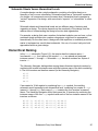
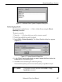
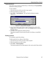
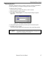
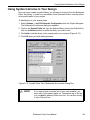
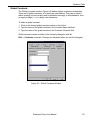
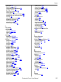
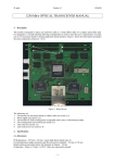
1
Schematic Entry User
Manual
Version 8.0
Technical Support Line: 1- 800-LATTICE or (408) 428-6414
DSNEXP-SCH-UM Rev 8.0.1
Copyright
This document may not, in whole or part, be copied, photocopied, reproduced,
translated, or reduced to any electronic medium or machine-readable form without
prior written consent from Lattice Semiconductor Corporation.
The software described in this manual is copyrighted and all rights are reserved by
Lattice Semiconductor Corporation. Information in this document is subject to change
without notice.
The distribution and sale of this product is intended for the use of the original
purchaser only and for use only on the computer system specified. Lawful users of
this product are hereby licensed only to read the programs on the disks, cassettes, or
tapes from their medium into the memory of a computer solely for the purpose of
executing them. Unauthorized copying, duplicating, selling, or otherwise distributing
this product is a violation of the law.
Trademarks
The following trademarks are recognized by Lattice Semiconductor Corporation:
Generic Array Logic, ISP, ispANALYZER, ispATE, ispCODE, ispDCD,
ispDOWNLOAD, ispDS, ispDS+, ispEXPERT, ispGDS, ispGDX, ispHDL, ispJTAG,
ispSmartFlow, ispStarter, ispSTREAM, ispSVF, ispTA, ispTEST, ispTURBO,
ispVECTOR, ispVerilog, ispVHDL, ispVM, Latch-Lock, LHDL, pDS+, RFT, and Twin
GLB are trademarks of Lattice Semiconductor Corporation.
E2CMOS, GAL, ispGAL, ispLSI, pDS, pLSI, Silicon Forest, and UltraMOS are
registered trademarks of Lattice Semiconductor Corporation.
Project Navigator is a trademark of Data I/O Corporation. ABEL-HDL is a registered
trademark of Data I/O Corporation.
Microsoft, Windows, and MS-DOS are registered trademarks of Microsoft
Corporation.
IBM is a registered trademark of International Business Machines Corporation.
Lattice Semiconductor Corporation
5555 NE Moore Ct.
Hillsboro, OR 97124
(503) 268-8000
December 1999
Schematic Entry User Manual
2
Limited Warranty
Lattice Semiconductor Corporation warrants the original purchaser that the Lattice
Semiconductor software shall be free from defects in material and workmanship for a
period of ninety days from the date of purchase. If a defect covered by this limited
warranty occurs during this 90-day warranty period, Lattice Semiconductor will repair
or replace the component part at its option free of charge.
This limited warranty does not apply if the defects have been caused by negligence,
accident, unreasonable or unintended use, modification, or any causes not related to
defective materials or workmanship.
To receive service during the 90-day warranty period, contact Lattice Semiconductor
Corporation at:
Phone: 1-800-LATTICE
Fax: (408) 944-8450
E-mail: [email protected]
If the Lattice Semiconductor support personnel are unable to solve your problem over
the phone, we will provide you with instructions on returning your defective software
to us. The cost of returning the software to the Lattice Semiconductor Service Center
shall be paid by the purchaser.
Limitations on Warranty
Any applicable implied warranties, including warranties of merchantability and fitness
for a particular purpose, are hereby limited to ninety days from the date of purchase
and are subject to the conditions set forth herein. In no event shall Lattice
Semiconductor Corporation be liable for consequential or incidental damages
resulting from the breach of any expressed or implied warranties.
Purchaser’s sole remedy for any cause whatsoever, regardless of the form of action,
shall be limited to the price paid to Lattice Semiconductor for the Lattice
Semiconductor software.
The provisions of this limited warranty are valid in the United States only. Some states
do not allow limitations on how long an implied warranty lasts, or exclusion of
consequential or incidental damages, so the above limitation or exclusion may not
apply to you.
This warranty provides you with specific legal rights. You may have other rights which
vary from state to state.
Schematic Entry User Manual
3
Table of Contents
Preface . . . . . . . . . . . . . . . . . . . . . . . . . . . . . . . . . . . . . . . . . . . . . . . . . . . . . . . . . . . . . . . . . . . 11
Where to Look for Information . . . . . . . . . . . . . . . . . . . . . . . . . . . . . . . . . . . . . . . . . . . . . . . . .
What is in this Manual . . . . . . . . . . . . . . . . . . . . . . . . . . . . . . . . . . . . . . . . . . . . . . . . . . . . . . .
Documentation Convention . . . . . . . . . . . . . . . . . . . . . . . . . . . . . . . . . . . . . . . . . . . . . . . . . . .
Related Documentation . . . . . . . . . . . . . . . . . . . . . . . . . . . . . . . . . . . . . . . . . . . . . . . . . . . . . .
12
13
14
15
Chapter 1 Inside SCS . . . . . . . . . . . . . . . . . . . . . . . . . . . . . . . . . . . . . . . . . . . . . . . . . . . . 16
What SCS Can Do . . . . . . . . . . . . . . . . . . . . . . . . . . . . . . . . . . . . . . . . . . . . . . . . . . . . . . . . . .
SCS Programs . . . . . . . . . . . . . . . . . . . . . . . . . . . . . . . . . . . . . . . . . . . . . . . . . . . . . . . . . . . . .
Symbols . . . . . . . . . . . . . . . . . . . . . . . . . . . . . . . . . . . . . . . . . . . . . . . . . . . . . . . . . . . . . . . . . .
Symbol Libraries. . . . . . . . . . . . . . . . . . . . . . . . . . . . . . . . . . . . . . . . . . . . . . . . . . . . . . . . .
What Does a Symbol Consist of?. . . . . . . . . . . . . . . . . . . . . . . . . . . . . . . . . . . . . . . . . . . .
Graphics . . . . . . . . . . . . . . . . . . . . . . . . . . . . . . . . . . . . . . . . . . . . . . . . . . . . . . . . . . . .
Pins . . . . . . . . . . . . . . . . . . . . . . . . . . . . . . . . . . . . . . . . . . . . . . . . . . . . . . . . . . . . . . . .
Attributes . . . . . . . . . . . . . . . . . . . . . . . . . . . . . . . . . . . . . . . . . . . . . . . . . . . . . . . . . . . .
Schematic Elements . . . . . . . . . . . . . . . . . . . . . . . . . . . . . . . . . . . . . . . . . . . . . . . . . . . . . . . .
Symbols . . . . . . . . . . . . . . . . . . . . . . . . . . . . . . . . . . . . . . . . . . . . . . . . . . . . . . . . . . . . . . .
Symbol Attributes . . . . . . . . . . . . . . . . . . . . . . . . . . . . . . . . . . . . . . . . . . . . . . . . . . . . .
Wires . . . . . . . . . . . . . . . . . . . . . . . . . . . . . . . . . . . . . . . . . . . . . . . . . . . . . . . . . . . . . . . . .
Wire Names . . . . . . . . . . . . . . . . . . . . . . . . . . . . . . . . . . . . . . . . . . . . . . . . . . . . . . . . .
Net Attributes . . . . . . . . . . . . . . . . . . . . . . . . . . . . . . . . . . . . . . . . . . . . . . . . . . . . . . . .
I/O Markers. . . . . . . . . . . . . . . . . . . . . . . . . . . . . . . . . . . . . . . . . . . . . . . . . . . . . . . . . . . . .
Graphics . . . . . . . . . . . . . . . . . . . . . . . . . . . . . . . . . . . . . . . . . . . . . . . . . . . . . . . . . . . . . . .
Text. . . . . . . . . . . . . . . . . . . . . . . . . . . . . . . . . . . . . . . . . . . . . . . . . . . . . . . . . . . . . . . . . . .
Schematics Relation to Netlists . . . . . . . . . . . . . . . . . . . . . . . . . . . . . . . . . . . . . . . . . . . . . . . .
Using Netlists . . . . . . . . . . . . . . . . . . . . . . . . . . . . . . . . . . . . . . . . . . . . . . . . . . . . . . . . . . .
17
18
18
18
18
18
19
19
19
20
21
21
21
22
22
22
22
23
23
Chapter 2 Introduction to Hierarchical Design . . . . . . . . . . . . . . . . . . . . . . . . . . . . 24
What is a Hierarchy? . . . . . . . . . . . . . . . . . . . . . . . . . . . . . . . . . . . . . . . . . . . . . . . . . . . . . . . .
Advantages of Hierarchical Design . . . . . . . . . . . . . . . . . . . . . . . . . . . . . . . . . . . . . . . . . . . . .
Approaches to Hierarchical Design . . . . . . . . . . . . . . . . . . . . . . . . . . . . . . . . . . . . . . . . . . . . .
Top-Down Design. . . . . . . . . . . . . . . . . . . . . . . . . . . . . . . . . . . . . . . . . . . . . . . . . . . . . . . .
Bottom-Up Design . . . . . . . . . . . . . . . . . . . . . . . . . . . . . . . . . . . . . . . . . . . . . . . . . . . . . . .
Inside-Out (“Mixed”) Design . . . . . . . . . . . . . . . . . . . . . . . . . . . . . . . . . . . . . . . . . . . . . . . .
What is Hierarchical Organization? . . . . . . . . . . . . . . . . . . . . . . . . . . . . . . . . . . . . . . . . . . . . .
Symbols, Schematics, and Hierarchy . . . . . . . . . . . . . . . . . . . . . . . . . . . . . . . . . . . . . . . . . . .
Hierarchical Design Structure . . . . . . . . . . . . . . . . . . . . . . . . . . . . . . . . . . . . . . . . . . . . . . . . .
Schematic Sheets Versus Hierarchical Levels . . . . . . . . . . . . . . . . . . . . . . . . . . . . . . . . . .
Schematic Entry User Manual
25
25
26
26
26
27
27
28
29
30
4
Hierarchical Naming. . . . . . . . . . . . . . . . . . . . . . . . . . . . . . . . . . . . . . . . . . . . . . . . . . . . . . . . . 30
Nets in the Hierarchy . . . . . . . . . . . . . . . . . . . . . . . . . . . . . . . . . . . . . . . . . . . . . . . . . . . . . . . . 31
Automatic Aliasing of Nets . . . . . . . . . . . . . . . . . . . . . . . . . . . . . . . . . . . . . . . . . . . . . . . . . 31
Chapter 3 Basic Operation . . . . . . . . . . . . . . . . . . . . . . . . . . . . . . . . . . . . . . . . . . . . . . . 32
SCS Command Structure . . . . . . . . . . . . . . . . . . . . . . . . . . . . . . . . . . . . . . . . . . . . . . . . . . . .
Using the Mouse . . . . . . . . . . . . . . . . . . . . . . . . . . . . . . . . . . . . . . . . . . . . . . . . . . . . . . . . . . .
Right Mouse Button Functions . . . . . . . . . . . . . . . . . . . . . . . . . . . . . . . . . . . . . . . . . . . . . .
Prompting and Error Messages . . . . . . . . . . . . . . . . . . . . . . . . . . . . . . . . . . . . . . . . . . . . . . . .
Error Recovery. . . . . . . . . . . . . . . . . . . . . . . . . . . . . . . . . . . . . . . . . . . . . . . . . . . . . . . . . . . . .
Network Operation . . . . . . . . . . . . . . . . . . . . . . . . . . . . . . . . . . . . . . . . . . . . . . . . . . . . . . . . . .
Naming Design Files . . . . . . . . . . . . . . . . . . . . . . . . . . . . . . . . . . . . . . . . . . . . . . . . . . . . . . . .
Saving the Schematic or Symbol . . . . . . . . . . . . . . . . . . . . . . . . . . . . . . . . . . . . . . . . . . . . . . .
The INI Editor. . . . . . . . . . . . . . . . . . . . . . . . . . . . . . . . . . . . . . . . . . . . . . . . . . . . . . . . . . . . . .
33
33
34
34
35
35
36
37
37
Chapter 4 Using the Schematic Editor . . . . . . . . . . . . . . . . . . . . . . . . . . . . . . . . . . . . 38
What is a Schematic? . . . . . . . . . . . . . . . . . . . . . . . . . . . . . . . . . . . . . . . . . . . . . . . . . . . . . . .
Schematic File Names . . . . . . . . . . . . . . . . . . . . . . . . . . . . . . . . . . . . . . . . . . . . . . . . . . . .
Schematic Components. . . . . . . . . . . . . . . . . . . . . . . . . . . . . . . . . . . . . . . . . . . . . . . . . . . . . .
Symbols . . . . . . . . . . . . . . . . . . . . . . . . . . . . . . . . . . . . . . . . . . . . . . . . . . . . . . . . . . . . . . .
Wires . . . . . . . . . . . . . . . . . . . . . . . . . . . . . . . . . . . . . . . . . . . . . . . . . . . . . . . . . . . . . . . . .
Attributes . . . . . . . . . . . . . . . . . . . . . . . . . . . . . . . . . . . . . . . . . . . . . . . . . . . . . . . . . . . . . .
Graphics and Text . . . . . . . . . . . . . . . . . . . . . . . . . . . . . . . . . . . . . . . . . . . . . . . . . . . . . . .
Adding Schematic Elements . . . . . . . . . . . . . . . . . . . . . . . . . . . . . . . . . . . . . . . . . . . . . . . . . .
Adding a Symbol . . . . . . . . . . . . . . . . . . . . . . . . . . . . . . . . . . . . . . . . . . . . . . . . . . . . . . . .
Placing the Symbol. . . . . . . . . . . . . . . . . . . . . . . . . . . . . . . . . . . . . . . . . . . . . . . . . . . . . . .
Adding Instance Names . . . . . . . . . . . . . . . . . . . . . . . . . . . . . . . . . . . . . . . . . . . . . . . . . . .
Supported Characters in Instance Names . . . . . . . . . . . . . . . . . . . . . . . . . . . . . . . . . .
Wiring the Schematic . . . . . . . . . . . . . . . . . . . . . . . . . . . . . . . . . . . . . . . . . . . . . . . . . . . . . . . .
Drawing Wires . . . . . . . . . . . . . . . . . . . . . . . . . . . . . . . . . . . . . . . . . . . . . . . . . . . . . . . . . .
Diagonal Wires . . . . . . . . . . . . . . . . . . . . . . . . . . . . . . . . . . . . . . . . . . . . . . . . . . . . . . .
Nets and Buses . . . . . . . . . . . . . . . . . . . . . . . . . . . . . . . . . . . . . . . . . . . . . . . . . . . . . . . . . . . .
Net Names . . . . . . . . . . . . . . . . . . . . . . . . . . . . . . . . . . . . . . . . . . . . . . . . . . . . . . . . . . . . .
Identification . . . . . . . . . . . . . . . . . . . . . . . . . . . . . . . . . . . . . . . . . . . . . . . . . . . . . . . . .
Interconnection . . . . . . . . . . . . . . . . . . . . . . . . . . . . . . . . . . . . . . . . . . . . . . . . . . . . . . .
Entering Net Names . . . . . . . . . . . . . . . . . . . . . . . . . . . . . . . . . . . . . . . . . . . . . . . . . . . . . .
Placing the Net Name. . . . . . . . . . . . . . . . . . . . . . . . . . . . . . . . . . . . . . . . . . . . . . . . . . . . .
Legal Characters in Net Names . . . . . . . . . . . . . . . . . . . . . . . . . . . . . . . . . . . . . . . . . .
Reserved Names . . . . . . . . . . . . . . . . . . . . . . . . . . . . . . . . . . . . . . . . . . . . . . . . . . . . .
Logical Inversion . . . . . . . . . . . . . . . . . . . . . . . . . . . . . . . . . . . . . . . . . . . . . . . . . . . . . .
Renaming a Net . . . . . . . . . . . . . . . . . . . . . . . . . . . . . . . . . . . . . . . . . . . . . . . . . . . . . . . . .
Specifying Signal Direction. . . . . . . . . . . . . . . . . . . . . . . . . . . . . . . . . . . . . . . . . . . . . . . . .
I/O Markers . . . . . . . . . . . . . . . . . . . . . . . . . . . . . . . . . . . . . . . . . . . . . . . . . . . . . . . . . .
Adding a Marker to a Net . . . . . . . . . . . . . . . . . . . . . . . . . . . . . . . . . . . . . . . . . . . . . . .
Buses . . . . . . . . . . . . . . . . . . . . . . . . . . . . . . . . . . . . . . . . . . . . . . . . . . . . . . . . . . . . . . . . .
Bus Types . . . . . . . . . . . . . . . . . . . . . . . . . . . . . . . . . . . . . . . . . . . . . . . . . . . . . . . . . . .
Bus Taps . . . . . . . . . . . . . . . . . . . . . . . . . . . . . . . . . . . . . . . . . . . . . . . . . . . . . . . . . . . .
Bus Pins . . . . . . . . . . . . . . . . . . . . . . . . . . . . . . . . . . . . . . . . . . . . . . . . . . . . . . . . . . . .
Schematic Entry User Manual
39
39
40
40
40
40
40
41
41
42
42
45
45
45
46
46
46
46
46
47
47
48
48
48
49
49
49
49
50
50
52
53
5
Nets on Iterated Instances . . . . . . . . . . . . . . . . . . . . . . . . . . . . . . . . . . . . . . . . . . . . . . . . .
Bus and Net Connections to Iterated Instances . . . . . . . . . . . . . . . . . . . . . . . . . . . . . . . . .
Wiring Constraints . . . . . . . . . . . . . . . . . . . . . . . . . . . . . . . . . . . . . . . . . . . . . . . . . . . . . . . . . .
Modifying the Schematics . . . . . . . . . . . . . . . . . . . . . . . . . . . . . . . . . . . . . . . . . . . . . . . . . . . .
Clipboard Commands. . . . . . . . . . . . . . . . . . . . . . . . . . . . . . . . . . . . . . . . . . . . . . . . . . . . .
Non-Clipboard Commands . . . . . . . . . . . . . . . . . . . . . . . . . . . . . . . . . . . . . . . . . . . . . . . . .
Debugging and Verifying a Schematic. . . . . . . . . . . . . . . . . . . . . . . . . . . . . . . . . . . . . . . . . . .
“Unconnected Pin” Message . . . . . . . . . . . . . . . . . . . . . . . . . . . . . . . . . . . . . . . . . . . . . . .
Schematic Editor Display Options . . . . . . . . . . . . . . . . . . . . . . . . . . . . . . . . . . . . . . . . . . . . . .
Schematic Sheets. . . . . . . . . . . . . . . . . . . . . . . . . . . . . . . . . . . . . . . . . . . . . . . . . . . . . . . .
Multiple Views . . . . . . . . . . . . . . . . . . . . . . . . . . . . . . . . . . . . . . . . . . . . . . . . . . . . . . . .
Resizing and Renumbering Sheets. . . . . . . . . . . . . . . . . . . . . . . . . . . . . . . . . . . . . . . .
Adding Blank Sheets. . . . . . . . . . . . . . . . . . . . . . . . . . . . . . . . . . . . . . . . . . . . . . . . . . .
Grids . . . . . . . . . . . . . . . . . . . . . . . . . . . . . . . . . . . . . . . . . . . . . . . . . . . . . . . . . . . . . . . . . .
Controlling Display and Graphics Options . . . . . . . . . . . . . . . . . . . . . . . . . . . . . . . . . . . . .
Display Options . . . . . . . . . . . . . . . . . . . . . . . . . . . . . . . . . . . . . . . . . . . . . . . . . . . . . . .
Graphic Options . . . . . . . . . . . . . . . . . . . . . . . . . . . . . . . . . . . . . . . . . . . . . . . . . . . . . .
Setting Attribute Values . . . . . . . . . . . . . . . . . . . . . . . . . . . . . . . . . . . . . . . . . . . . . . . . . . . . . .
Pin Attributes . . . . . . . . . . . . . . . . . . . . . . . . . . . . . . . . . . . . . . . . . . . . . . . . . . . . . . . . . . .
Symbol Attributes . . . . . . . . . . . . . . . . . . . . . . . . . . . . . . . . . . . . . . . . . . . . . . . . . . . . . . . .
Finding Symbols with Specific Attributes . . . . . . . . . . . . . . . . . . . . . . . . . . . . . . . . . . .
Net Attributes . . . . . . . . . . . . . . . . . . . . . . . . . . . . . . . . . . . . . . . . . . . . . . . . . . . . . . . . . . .
Attribute Windows. . . . . . . . . . . . . . . . . . . . . . . . . . . . . . . . . . . . . . . . . . . . . . . . . . . . . . . .
53
54
55
55
55
56
57
58
58
58
58
58
59
59
59
60
61
62
62
62
63
64
65
Chapter 5 Using the Symbol Editor . . . . . . . . . . . . . . . . . . . . . . . . . . . . . . . . . . . . . . . 66
Symbol Components . . . . . . . . . . . . . . . . . . . . . . . . . . . . . . . . . . . . . . . . . . . . . . . . . . . . . . . .
Graphics . . . . . . . . . . . . . . . . . . . . . . . . . . . . . . . . . . . . . . . . . . . . . . . . . . . . . . . . . . . . . . .
Pins. . . . . . . . . . . . . . . . . . . . . . . . . . . . . . . . . . . . . . . . . . . . . . . . . . . . . . . . . . . . . . . . . . .
Attributes . . . . . . . . . . . . . . . . . . . . . . . . . . . . . . . . . . . . . . . . . . . . . . . . . . . . . . . . . . . . . .
Symbol Types . . . . . . . . . . . . . . . . . . . . . . . . . . . . . . . . . . . . . . . . . . . . . . . . . . . . . . . . . . . . .
Block Symbols . . . . . . . . . . . . . . . . . . . . . . . . . . . . . . . . . . . . . . . . . . . . . . . . . . . . . . . . . .
Cell Symbols. . . . . . . . . . . . . . . . . . . . . . . . . . . . . . . . . . . . . . . . . . . . . . . . . . . . . . . . . . . .
Graphic Symbols . . . . . . . . . . . . . . . . . . . . . . . . . . . . . . . . . . . . . . . . . . . . . . . . . . . . . . . .
Master Symbols . . . . . . . . . . . . . . . . . . . . . . . . . . . . . . . . . . . . . . . . . . . . . . . . . . . . . . . . .
Positioning Master Symbols . . . . . . . . . . . . . . . . . . . . . . . . . . . . . . . . . . . . . . . . . . . . .
Creating Symbols. . . . . . . . . . . . . . . . . . . . . . . . . . . . . . . . . . . . . . . . . . . . . . . . . . . . . . . . . . .
Starting the Symbol Editor . . . . . . . . . . . . . . . . . . . . . . . . . . . . . . . . . . . . . . . . . . . . . . . . .
Grids . . . . . . . . . . . . . . . . . . . . . . . . . . . . . . . . . . . . . . . . . . . . . . . . . . . . . . . . . . . . . . . . . .
Positioning Pins. . . . . . . . . . . . . . . . . . . . . . . . . . . . . . . . . . . . . . . . . . . . . . . . . . . . . . .
Drawing Graphics and Fixed Text . . . . . . . . . . . . . . . . . . . . . . . . . . . . . . . . . . . . . . . . . . .
Lines . . . . . . . . . . . . . . . . . . . . . . . . . . . . . . . . . . . . . . . . . . . . . . . . . . . . . . . . . . . . . . .
Rectangles . . . . . . . . . . . . . . . . . . . . . . . . . . . . . . . . . . . . . . . . . . . . . . . . . . . . . . . . . .
Circles and Arcs . . . . . . . . . . . . . . . . . . . . . . . . . . . . . . . . . . . . . . . . . . . . . . . . . . . . . .
Negation Bubbles . . . . . . . . . . . . . . . . . . . . . . . . . . . . . . . . . . . . . . . . . . . . . . . . . . . . .
Text . . . . . . . . . . . . . . . . . . . . . . . . . . . . . . . . . . . . . . . . . . . . . . . . . . . . . . . . . . . . . . . .
Text Size & Justification . . . . . . . . . . . . . . . . . . . . . . . . . . . . . . . . . . . . . . . . . . . . . . . .
Saving a Symbol. . . . . . . . . . . . . . . . . . . . . . . . . . . . . . . . . . . . . . . . . . . . . . . . . . . . . . . . .
Printing the Symbol . . . . . . . . . . . . . . . . . . . . . . . . . . . . . . . . . . . . . . . . . . . . . . . . . . . . . .
Schematic Entry User Manual
67
67
67
67
67
68
68
68
68
68
69
69
70
70
70
71
71
71
71
71
71
72
72
6
Editing Symbols . . . . . . . . . . . . . . . . . . . . . . . . . . . . . . . . . . . . . . . . . . . . . . . . . . . . . . . . .
Clipboard Commands . . . . . . . . . . . . . . . . . . . . . . . . . . . . . . . . . . . . . . . . . . . . . . . . . .
Non-Clipboard Commands . . . . . . . . . . . . . . . . . . . . . . . . . . . . . . . . . . . . . . . . . . . . . .
Preparing Symbols for Schematics . . . . . . . . . . . . . . . . . . . . . . . . . . . . . . . . . . . . . . . . . . . . .
Pins. . . . . . . . . . . . . . . . . . . . . . . . . . . . . . . . . . . . . . . . . . . . . . . . . . . . . . . . . . . . . . . . . . .
Adding Pins . . . . . . . . . . . . . . . . . . . . . . . . . . . . . . . . . . . . . . . . . . . . . . . . . . . . . . . . . .
Adding Pin Names . . . . . . . . . . . . . . . . . . . . . . . . . . . . . . . . . . . . . . . . . . . . . . . . . . . .
Displaying Pin Names . . . . . . . . . . . . . . . . . . . . . . . . . . . . . . . . . . . . . . . . . . . . . . . . . .
Displaying Pin Numbers . . . . . . . . . . . . . . . . . . . . . . . . . . . . . . . . . . . . . . . . . . . . . . . .
Bus Pins . . . . . . . . . . . . . . . . . . . . . . . . . . . . . . . . . . . . . . . . . . . . . . . . . . . . . . . . . . . . . . .
Bus Pin Limitations . . . . . . . . . . . . . . . . . . . . . . . . . . . . . . . . . . . . . . . . . . . . . . . . . . . .
Setting Origin . . . . . . . . . . . . . . . . . . . . . . . . . . . . . . . . . . . . . . . . . . . . . . . . . . . . . . . . . . .
Checking Symbols . . . . . . . . . . . . . . . . . . . . . . . . . . . . . . . . . . . . . . . . . . . . . . . . . . . . . . .
“Unconnected Pin” Message. . . . . . . . . . . . . . . . . . . . . . . . . . . . . . . . . . . . . . . . . . . . .
Creating Block Symbols in the Schematic Editor. . . . . . . . . . . . . . . . . . . . . . . . . . . . . . . . . . .
Making a Block Symbol for the Loaded Schematic . . . . . . . . . . . . . . . . . . . . . . . . . . . . . .
Making a Block Symbol for the Selected .naf File . . . . . . . . . . . . . . . . . . . . . . . . . . . . . . .
72
72
73
73
73
73
74
74
75
75
75
76
76
77
77
78
79
Chapter 6 Using the Library Manager . . . . . . . . . . . . . . . . . . . . . . . . . . . . . . . . . . . . . 80
Library Manager Overview. . . . . . . . . . . . . . . . . . . . . . . . . . . . . . . . . . . . . . . . . . . . . . . . . . . .
Symbol List . . . . . . . . . . . . . . . . . . . . . . . . . . . . . . . . . . . . . . . . . . . . . . . . . . . . . . . . . .
Symbol Diagram . . . . . . . . . . . . . . . . . . . . . . . . . . . . . . . . . . . . . . . . . . . . . . . . . . . . . .
Manipulating Binary Libraries. . . . . . . . . . . . . . . . . . . . . . . . . . . . . . . . . . . . . . . . . . . . . . . . . .
Creating Library . . . . . . . . . . . . . . . . . . . . . . . . . . . . . . . . . . . . . . . . . . . . . . . . . . . . . . . . .
Opening Library . . . . . . . . . . . . . . . . . . . . . . . . . . . . . . . . . . . . . . . . . . . . . . . . . . . . . . . . .
Adding Symbols . . . . . . . . . . . . . . . . . . . . . . . . . . . . . . . . . . . . . . . . . . . . . . . . . . . . . . . . .
Viewing Symbol Information . . . . . . . . . . . . . . . . . . . . . . . . . . . . . . . . . . . . . . . . . . . . . . . .
Extracting Symbols. . . . . . . . . . . . . . . . . . . . . . . . . . . . . . . . . . . . . . . . . . . . . . . . . . . . . . .
Copying Symbols . . . . . . . . . . . . . . . . . . . . . . . . . . . . . . . . . . . . . . . . . . . . . . . . . . . . . . . .
Deleting Symbols . . . . . . . . . . . . . . . . . . . . . . . . . . . . . . . . . . . . . . . . . . . . . . . . . . . . . . . .
Renaming Symbols . . . . . . . . . . . . . . . . . . . . . . . . . . . . . . . . . . . . . . . . . . . . . . . . . . . . . .
Using Symbol Libraries in Your Design . . . . . . . . . . . . . . . . . . . . . . . . . . . . . . . . . . . . . . . . . .
81
82
82
82
82
82
83
84
85
86
86
87
88
Chapter 7 Using the Hierarchy Navigator . . . . . . . . . . . . . . . . . . . . . . . . . . . . . . . . . 89
Hierarchy Navigator Functions. . . . . . . . . . . . . . . . . . . . . . . . . . . . . . . . . . . . . . . . . . . . . . . . .
Navigating a Design. . . . . . . . . . . . . . . . . . . . . . . . . . . . . . . . . . . . . . . . . . . . . . . . . . . . . . . . .
Updating Schematics . . . . . . . . . . . . . . . . . . . . . . . . . . . . . . . . . . . . . . . . . . . . . . . . . . . . .
Push/Pop . . . . . . . . . . . . . . . . . . . . . . . . . . . . . . . . . . . . . . . . . . . . . . . . . . . . . . . . . . . . . .
Tracing Signals . . . . . . . . . . . . . . . . . . . . . . . . . . . . . . . . . . . . . . . . . . . . . . . . . . . . . . . . . . . .
Setting and Overriding Attributes . . . . . . . . . . . . . . . . . . . . . . . . . . . . . . . . . . . . . . . . . . . . . . .
Pin Attributes . . . . . . . . . . . . . . . . . . . . . . . . . . . . . . . . . . . . . . . . . . . . . . . . . . . . . . . . . . .
Symbol Attributes . . . . . . . . . . . . . . . . . . . . . . . . . . . . . . . . . . . . . . . . . . . . . . . . . . . . . . . .
Net Attributes . . . . . . . . . . . . . . . . . . . . . . . . . . . . . . . . . . . . . . . . . . . . . . . . . . . . . . . . . . .
Attribute Windows. . . . . . . . . . . . . . . . . . . . . . . . . . . . . . . . . . . . . . . . . . . . . . . . . . . . . . . .
Additional Hierarchy Navigator Features . . . . . . . . . . . . . . . . . . . . . . . . . . . . . . . . . . . . . . . . .
Save . . . . . . . . . . . . . . . . . . . . . . . . . . . . . . . . . . . . . . . . . . . . . . . . . . . . . . . . . . . . . . . . . .
Sheets . . . . . . . . . . . . . . . . . . . . . . . . . . . . . . . . . . . . . . . . . . . . . . . . . . . . . . . . . . . . . . . .
Print . . . . . . . . . . . . . . . . . . . . . . . . . . . . . . . . . . . . . . . . . . . . . . . . . . . . . . . . . . . . . . . . . .
Schematic Entry User Manual
90
90
90
91
92
94
94
94
95
95
95
95
95
96
7
Display Options . . . . . . . . . . . . . . . . . . . . . . . . . . . . . . . . . . . . . . . . . . . . . . . . . . . . . . . . .
Statistics . . . . . . . . . . . . . . . . . . . . . . . . . . . . . . . . . . . . . . . . . . . . . . . . . . . . . . . . . . . . . . .
Analysis Tools . . . . . . . . . . . . . . . . . . . . . . . . . . . . . . . . . . . . . . . . . . . . . . . . . . . . . . . . . . . . .
The View Report Utility . . . . . . . . . . . . . . . . . . . . . . . . . . . . . . . . . . . . . . . . . . . . . . . . . . . .
Viewing Critical Paths. . . . . . . . . . . . . . . . . . . . . . . . . . . . . . . . . . . . . . . . . . . . . . . . . . . . .
96
96
97
97
98
Chapter 8 Attributes . . . . . . . . . . . . . . . . . . . . . . . . . . . . . . . . . . . . . . . . . . . . . . . . . . . . . 99
Attribute Functions . . . . . . . . . . . . . . . . . . . . . . . . . . . . . . . . . . . . . . . . . . . . . . . . . . . . . . . . .
Attribute Types. . . . . . . . . . . . . . . . . . . . . . . . . . . . . . . . . . . . . . . . . . . . . . . . . . . . . . . . . . . .
Attribute Components . . . . . . . . . . . . . . . . . . . . . . . . . . . . . . . . . . . . . . . . . . . . . . . . . . . . . .
Attributes . . . . . . . . . . . . . . . . . . . . . . . . . . . . . . . . . . . . . . . . . . . . . . . . . . . . . . . . . . . . .
Pin Attributes. . . . . . . . . . . . . . . . . . . . . . . . . . . . . . . . . . . . . . . . . . . . . . . . . . . . . . . .
Symbol Attributes . . . . . . . . . . . . . . . . . . . . . . . . . . . . . . . . . . . . . . . . . . . . . . . . . . . .
Attribute Windows. . . . . . . . . . . . . . . . . . . . . . . . . . . . . . . . . . . . . . . . . . . . . . . . . . . . . . .
Attribute Name . . . . . . . . . . . . . . . . . . . . . . . . . . . . . . . . . . . . . . . . . . . . . . . . . . . . . . . . .
Attribute Number . . . . . . . . . . . . . . . . . . . . . . . . . . . . . . . . . . . . . . . . . . . . . . . . . . . . . . .
Attribute Value . . . . . . . . . . . . . . . . . . . . . . . . . . . . . . . . . . . . . . . . . . . . . . . . . . . . . . . . .
Attribute Modifier . . . . . . . . . . . . . . . . . . . . . . . . . . . . . . . . . . . . . . . . . . . . . . . . . . . . . . .
Modifying Attributes . . . . . . . . . . . . . . . . . . . . . . . . . . . . . . . . . . . . . . . . . . . . . . . . . . . . . . . .
Symbol Attributes . . . . . . . . . . . . . . . . . . . . . . . . . . . . . . . . . . . . . . . . . . . . . . . . . . . . . . .
Pin Attributes . . . . . . . . . . . . . . . . . . . . . . . . . . . . . . . . . . . . . . . . . . . . . . . . . . . . . . . . . .
Net Attributes . . . . . . . . . . . . . . . . . . . . . . . . . . . . . . . . . . . . . . . . . . . . . . . . . . . . . . . . . .
Creating New Attributes . . . . . . . . . . . . . . . . . . . . . . . . . . . . . . . . . . . . . . . . . . . . . . . . . . . . .
Attribute Names . . . . . . . . . . . . . . . . . . . . . . . . . . . . . . . . . . . . . . . . . . . . . . . . . . . . . . . .
Attribute Modifiers. . . . . . . . . . . . . . . . . . . . . . . . . . . . . . . . . . . . . . . . . . . . . . . . . . . . . . .
Assigning Values to Simple Attributes . . . . . . . . . . . . . . . . . . . . . . . . . . . . . . . . . . . . . . .
Changing Attribute Values in the Schematic Editor . . . . . . . . . . . . . . . . . . . . . . . . . .
Removing Attributes from a Netlist . . . . . . . . . . . . . . . . . . . . . . . . . . . . . . . . . . . . . . .
Displaying Attribute Values on a Schematic . . . . . . . . . . . . . . . . . . . . . . . . . . . . . . . .
Reassigning Attribute Windows . . . . . . . . . . . . . . . . . . . . . . . . . . . . . . . . . . . . . . . . .
Number Notation in Attributes . . . . . . . . . . . . . . . . . . . . . . . . . . . . . . . . . . . . . . . . . . . . . . . .
Derived Attributes . . . . . . . . . . . . . . . . . . . . . . . . . . . . . . . . . . . . . . . . . . . . . . . . . . . . . . . . .
Examples of Derived Attributes . . . . . . . . . . . . . . . . . . . . . . . . . . . . . . . . . . . . . . . . . . . .
Calculated Derived Attributes . . . . . . . . . . . . . . . . . . . . . . . . . . . . . . . . . . . . . . . . . . . . . .
Derived Attributes and Hierarchy . . . . . . . . . . . . . . . . . . . . . . . . . . . . . . . . . . . . . . . . . . .
Example of Derived Attributes. . . . . . . . . . . . . . . . . . . . . . . . . . . . . . . . . . . . . . . . . . .
100
100
101
101
101
101
102
103
103
103
103
104
104
104
104
104
106
106
108
108
108
109
109
111
112
113
115
116
116
Chapter 9 The SCS INI Editor . . . . . . . . . . . . . . . . . . . . . . . . . . . . . . . . . . . . . . . . . . . . 119
Custom INI Files . . . . . . . . . . . . . . . . . . . . . . . . . . . . . . . . . . . . . . . . . . . . . . . . . . . . . . . . . .
Master and Device Mode . . . . . . . . . . . . . . . . . . . . . . . . . . . . . . . . . . . . . . . . . . . . . . . . .
Design Options . . . . . . . . . . . . . . . . . . . . . . . . . . . . . . . . . . . . . . . . . . . . . . . . . . . . . . . . .
Bus Parentheses. . . . . . . . . . . . . . . . . . . . . . . . . . . . . . . . . . . . . . . . . . . . . . . . . . . . .
Prefer Descending Buses . . . . . . . . . . . . . . . . . . . . . . . . . . . . . . . . . . . . . . . . . . . . . .
First Character Must be Alphabetic. . . . . . . . . . . . . . . . . . . . . . . . . . . . . . . . . . . . . . .
Coerce Net Names to Upper Case . . . . . . . . . . . . . . . . . . . . . . . . . . . . . . . . . . . . . . .
Coerce Attributes to Upper Case . . . . . . . . . . . . . . . . . . . . . . . . . . . . . . . . . . . . . . . .
Text Viewer . . . . . . . . . . . . . . . . . . . . . . . . . . . . . . . . . . . . . . . . . . . . . . . . . . . . . . . . .
Text Editor. . . . . . . . . . . . . . . . . . . . . . . . . . . . . . . . . . . . . . . . . . . . . . . . . . . . . . . . . .
Schematic Entry User Manual
120
120
120
120
120
121
121
121
121
121
8
System Controls . . . . . . . . . . . . . . . . . . . . . . . . . . . . . . . . . . . . . . . . . . . . . . . . . . . . . . . .
Show Off-Page Connections. . . . . . . . . . . . . . . . . . . . . . . . . . . . . . . . . . . . . . . . . . . .
Show Solder Dots . . . . . . . . . . . . . . . . . . . . . . . . . . . . . . . . . . . . . . . . . . . . . . . . . . . .
Show Open Ends . . . . . . . . . . . . . . . . . . . . . . . . . . . . . . . . . . . . . . . . . . . . . . . . . . . .
Show Border . . . . . . . . . . . . . . . . . . . . . . . . . . . . . . . . . . . . . . . . . . . . . . . . . . . . . . . .
Default Pin Name Offset . . . . . . . . . . . . . . . . . . . . . . . . . . . . . . . . . . . . . . . . . . . . . . .
Sheet Layout . . . . . . . . . . . . . . . . . . . . . . . . . . . . . . . . . . . . . . . . . . . . . . . . . . . . . . . . . .
Sheet Zones . . . . . . . . . . . . . . . . . . . . . . . . . . . . . . . . . . . . . . . . . . . . . . . . . . . . . . . .
Grid . . . . . . . . . . . . . . . . . . . . . . . . . . . . . . . . . . . . . . . . . . . . . . . . . . . . . . . . . . . . . . .
Master Symbols . . . . . . . . . . . . . . . . . . . . . . . . . . . . . . . . . . . . . . . . . . . . . . . . . . . . .
Sheet Sizes . . . . . . . . . . . . . . . . . . . . . . . . . . . . . . . . . . . . . . . . . . . . . . . . . . . . . . . . . . .
Global Nets. . . . . . . . . . . . . . . . . . . . . . . . . . . . . . . . . . . . . . . . . . . . . . . . . . . . . . . . . . . .
Attributes Tabs. . . . . . . . . . . . . . . . . . . . . . . . . . . . . . . . . . . . . . . . . . . . . . . . . . . . . . . . . . . .
Symbol, Pin, and Net Attributes . . . . . . . . . . . . . . . . . . . . . . . . . . . . . . . . . . . . . . . . . . . .
Attribute Numbers . . . . . . . . . . . . . . . . . . . . . . . . . . . . . . . . . . . . . . . . . . . . . . . . . . . .
Adding Attributes. . . . . . . . . . . . . . . . . . . . . . . . . . . . . . . . . . . . . . . . . . . . . . . . . . . . .
Attribute Data Fields . . . . . . . . . . . . . . . . . . . . . . . . . . . . . . . . . . . . . . . . . . . . . . . . . .
Modifying Attributes. . . . . . . . . . . . . . . . . . . . . . . . . . . . . . . . . . . . . . . . . . . . . . . . . . .
Example Attributes . . . . . . . . . . . . . . . . . . . . . . . . . . . . . . . . . . . . . . . . . . . . . . . . . . . . . .
Global Constants . . . . . . . . . . . . . . . . . . . . . . . . . . . . . . . . . . . . . . . . . . . . . . . . . . . . . . .
Search Paths Tabs . . . . . . . . . . . . . . . . . . . . . . . . . . . . . . . . . . . . . . . . . . . . . . . . . . . . . . . .
Project, Model, and Symbol Paths . . . . . . . . . . . . . . . . . . . . . . . . . . . . . . . . . . . . . . . . . .
Adding and Deleting Elements to Paths . . . . . . . . . . . . . . . . . . . . . . . . . . . . . . . . . . .
Libraries and Directory Structures . . . . . . . . . . . . . . . . . . . . . . . . . . . . . . . . . . . . . . . . . . . . .
Program Directories . . . . . . . . . . . . . . . . . . . . . . . . . . . . . . . . . . . . . . . . . . . . . . . . . . . . .
User Directories . . . . . . . . . . . . . . . . . . . . . . . . . . . . . . . . . . . . . . . . . . . . . . . . . . . . . . . .
Library Directories . . . . . . . . . . . . . . . . . . . . . . . . . . . . . . . . . . . . . . . . . . . . . . . . . . . . . .
Project Directories. . . . . . . . . . . . . . . . . . . . . . . . . . . . . . . . . . . . . . . . . . . . . . . . . . . .
Symbol Libraries . . . . . . . . . . . . . . . . . . . . . . . . . . . . . . . . . . . . . . . . . . . . . . . . . . . . .
Model Libraries . . . . . . . . . . . . . . . . . . . . . . . . . . . . . . . . . . . . . . . . . . . . . . . . . . . . . .
Library Searching . . . . . . . . . . . . . . . . . . . . . . . . . . . . . . . . . . . . . . . . . . . . . . . . . . . .
121
121
121
122
122
122
122
122
122
123
123
124
126
126
128
128
128
129
129
131
132
132
133
134
134
134
134
135
135
135
135
Appendix A Generic Interfaces . . . . . . . . . . . . . . . . . . . . . . . . . . . . . . . . . . . . . . . . . . 137
Archive Utility . . . . . . . . . . . . . . . . . . . . . . . . . . . . . . . . . . . . . . . . . . . . . . . . . . . . . . . . . . . . .
ASCII Interface. . . . . . . . . . . . . . . . . . . . . . . . . . . . . . . . . . . . . . . . . . . . . . . . . . . . . . . . . . . .
ASCII/Schematic Interface . . . . . . . . . . . . . . . . . . . . . . . . . . . . . . . . . . . . . . . . . . . . . . . .
Interface Format . . . . . . . . . . . . . . . . . . . . . . . . . . . . . . . . . . . . . . . . . . . . . . . . . . . . .
SCS Database Version. . . . . . . . . . . . . . . . . . . . . . . . . . . . . . . . . . . . . . . . . . . . . . . . . . .
Sheet Size . . . . . . . . . . . . . . . . . . . . . . . . . . . . . . . . . . . . . . . . . . . . . . . . . . . . . . . . . . . .
Net Position (Wire) . . . . . . . . . . . . . . . . . . . . . . . . . . . . . . . . . . . . . . . . . . . . . . . . . . . . . .
Flag Position. . . . . . . . . . . . . . . . . . . . . . . . . . . . . . . . . . . . . . . . . . . . . . . . . . . . . . . . . . .
Pin Position and Definition . . . . . . . . . . . . . . . . . . . . . . . . . . . . . . . . . . . . . . . . . . . . . . . .
Bus Tap Position . . . . . . . . . . . . . . . . . . . . . . . . . . . . . . . . . . . . . . . . . . . . . . . . . . . . . . .
Symbol Position and Format . . . . . . . . . . . . . . . . . . . . . . . . . . . . . . . . . . . . . . . . . . . . . .
Attribute Window Position. . . . . . . . . . . . . . . . . . . . . . . . . . . . . . . . . . . . . . . . . . . . . . . . .
Pin Attribute Position . . . . . . . . . . . . . . . . . . . . . . . . . . . . . . . . . . . . . . . . . . . . . . . . . . . .
Net Attribute Position . . . . . . . . . . . . . . . . . . . . . . . . . . . . . . . . . . . . . . . . . . . . . . . . . . . .
Lines . . . . . . . . . . . . . . . . . . . . . . . . . . . . . . . . . . . . . . . . . . . . . . . . . . . . . . . . . . . . . . . . .
Schematic Entry User Manual
138
138
139
140
140
140
140
141
141
141
141
142
143
143
143
9
Rectangles . . . . . . . . . . . . . . . . . . . . . . . . . . . . . . . . . . . . . . . . . . . . . . . . . . . . . . . . . . . .
Circles. . . . . . . . . . . . . . . . . . . . . . . . . . . . . . . . . . . . . . . . . . . . . . . . . . . . . . . . . . . . . . . .
Arcs . . . . . . . . . . . . . . . . . . . . . . . . . . . . . . . . . . . . . . . . . . . . . . . . . . . . . . . . . . . . . . . . .
Table Text Position. . . . . . . . . . . . . . . . . . . . . . . . . . . . . . . . . . . . . . . . . . . . . . . . . . . . . .
Font Parameters. . . . . . . . . . . . . . . . . . . . . . . . . . . . . . . . . . . . . . . . . . . . . . . . . . . . . . . .
Table Name and Title Attributes . . . . . . . . . . . . . . . . . . . . . . . . . . . . . . . . . . . . . . . . . . . .
EDIF Interfaces . . . . . . . . . . . . . . . . . . . . . . . . . . . . . . . . . . . . . . . . . . . . . . . . . . . . . . . . . . .
EDIF Netlist Interface . . . . . . . . . . . . . . . . . . . . . . . . . . . . . . . . . . . . . . . . . . . . . . . . . . . .
EDIF File Format . . . . . . . . . . . . . . . . . . . . . . . . . . . . . . . . . . . . . . . . . . . . . . . . . . . . . . .
Scaling . . . . . . . . . . . . . . . . . . . . . . . . . . . . . . . . . . . . . . . . . . . . . . . . . . . . . . . . . . . .
Renaming Object Names . . . . . . . . . . . . . . . . . . . . . . . . . . . . . . . . . . . . . . . . . . . . . .
Formatting EDIF Files. . . . . . . . . . . . . . . . . . . . . . . . . . . . . . . . . . . . . . . . . . . . . . . . . . . .
Preparing Non-SCS EDIF Files for Translation. . . . . . . . . . . . . . . . . . . . . . . . . . . . . .
Generic Netlists . . . . . . . . . . . . . . . . . . . . . . . . . . . . . . . . . . . . . . . . . . . . . . . . . . . . . . . . . . .
Netlist by Net (netorder) . . . . . . . . . . . . . . . . . . . . . . . . . . . . . . . . . . . . . . . . . . . . . . . . . .
Netlist by Pin (pinorder) . . . . . . . . . . . . . . . . . . . . . . . . . . . . . . . . . . . . . . . . . . . . . . . . . .
Schematic Entry User Manual
143
144
144
144
145
146
147
147
147
149
149
149
150
151
152
153
10
Preface
This manual describes the ispDesignExpert Schematic Capture System (SCS). It is
divided into two sections. The first section presents the “what” of SCS, the last
section the “how.” You do not have to read the first section in order to use SCS.
However, it has background information that should increase your understanding of
the SCS’s features, and lets you take fuller advantage of them. Chapter 3, Basic
Operation explains how to configure SCS.
Schematic Entry User Manual
11
Where to Look for Information
Where to Look for Information
The following is a brief outline of the contents in each chapter:
Chapter 1, Inside SCS – Explains what an SCS symbol is, and how its
characteristics and behavior are controlled by attributes. Describes the components
that make up an SCS schematic and how they relate to netlists.
Chapter 2, Introduction to Hierarchical Design – Shows how SCS schematics can
be combined into a hierarchical structure, and describes the advantages of
hierarchical design. Three approaches to hierarchical design are explained. Also
describes the principles of hierarchical organization used in the Schematic Editor and
Hierarchy Navigator.
Chapter 3, Basic Operation – Discusses the interface and common features of the
Schematic and Symbol Editors. Also explains how to configure the SCS Executive
program and explains the principal features of SCS.
Chapter 4, Using the Schematic Editor – Covers most of what you need to know to
add symbols and wiring to a schematic. Explains what nets and buses are, how to
create them, and how to name them.
Chapter 5, Using the Symbol Editor – Shows how to create your own symbols and
attach attributes to them. Block symbols (symbols that represent modules or
sub-circuits) are also described.
Chapter 6, Using the Library Manager – Explains what symbol libraries are and
how the Library Manager works. Also shows how to manipulate binary libraries and
use symbol libraries in your design.
Chapter 7, Using the Hierarchy Navigator – Shows how to view and probe each
level of a design using the Hierarchy Navigator. Explains the operation of the
Electrical Rules Checker and the Critical Path Viewer.
Chapter 8, Attributes – Explains what an attribute is and how attributes are
assigned to symbols, pins, and nets. Derived attributes, which permit dynamic
modification of a design, are also described.
Chapter 9, The SCS INI Editor – Explains how the Schematic and Symbol Editors,
Hierarchy Navigator, Waveform Viewer and Waveform Editor are configured by
changing values and settings with the INI Editor.
Appendix A, Generic Interfaces – Describes the general-purpose interfaces that
are most often used to move the design between systems.
Schematic Entry User Manual
12
What is in this Manual
What is in this Manual
This manual covers the following tools information:
■
■
■
■
■
■
■
Schematic Editor
The Schematic Editor is SCS’s schematic-capture tool. It creates schematic
(.sch) files that can represent a complete design, or any component of a
hierarchical design.
Symbol Editor
SCS comes with a standard symbol library for ispLSI design. The Symbol Editor is
used to create symbols or primitive elements that represent an independent
schematic module. You can also create decorative symbols (such as title blocks).
Library Manager
The Library Manager manages libraries of symbols that are used in schematics in
ispDesignExpert. You can browse through the libraries and maintain the libraries
by adding, deleting, extracting, or renaming the symbol files in the libraries.
Hierarchy Navigator
The Hierarchy Navigator combines all the components of a multi-level design for
viewing and analysis. You can traverse the full design, viewing each component in
its full hierarchical context.
INI Editor
The INI Editor modifies SCS INI files, which control the appearance and behavior
of SCS. Using the INI Editor, you can set your own preferences for how the SCS
environment looks and behaves. The INI Editor also manages attributes that
define the electrical behavior of symbols, pins, and nets.
Waveform Viewer
The Waveform Viewer is used to view the results of simulation. You can display
the waveform of any net in your design. The Viewer is fully interactive with the
Hierarchy Navigator; clicking on a net in the schematic automatically displays the
waveform. Waveform Viewer operation is covered in the Design Verification
Tools User Manual.
Waveform Editor
The Waveform Editor lets you create the stimulus waveforms for simulation
graphically, by drawing directly on the screen. The stimuli can be edited
graphically, or by modifying values in dialog boxes. The Editor then converts the
waveforms into a stimulus file that your simulator recognizes. Waveform files are
also useful as input to automatic test equipment, or as documentation of the
circuit’s expected behavior. Waveform Editor operation is covered in the Design
Verification Tools User Manual.
Schematic Entry User Manual
13
Documentation Convention
Documentation Convention
This user manual follows the typographic conventions listed here:
Convention
Definition and Usage
Italics
Italicized text represents variable input. For example:
project.wdl
This means you must replace project with the file name you used for all the
files relevant to your design.
Valuable information may be italicized for emphasis. Book titles also appear in
italics.
The beginning of a procedure appears in italics. For example:
To run the functional simulation:
Bold
Valuable information may be boldfaced for emphasis. Commands are shown in
boldface. For example:
Select Add ⇒ Pin from the Symbol Editor.
Courier
Font
Monospaced (Courier) font indicates file and directory names and text that the
system displays. For example:
The C:\ISPTOOLS\ISPSYS\CONFIG subdirectory contains...
Bold
Courier
Bold Courier font indicates text you type in response to system prompts. For
example:
SET YBUS [Y0..Y6];
|...|
Vertical bars indicate options that are mutually exclusive; you can select only one.
For example:
INPUT|OUTPUT|BIDI
“Quotes”
Titles of chapters or sections in chapters in this manual are shown in quotation
marks. For example:
See Chapter 1, “Inside SCS.”
✍ NOTE
Indicates a special note.
▲ CAUTION
Indicates a situation that could cause loss of data or other problems.
❖ TIP
Indicates a special hint that makes using the software easier.
⇒
Indicates a menu option leading to a submenu option. For example:
File ⇒ New
Schematic Entry User Manual
14
Related Documentation
Related Documentation
In addition to this manual, you might find the following reference material helpful:
■
■
■
■
■
■
■
■
■
■
■
ispDesignExpert User Manual
ispDesignExpert Tutorial
Design Verification Tools User Manual
ispLSI Macro Library Reference Manual
ispLSI 5K/8K Macro Library Supplement
ABEL Design Manual
ABEL-HDL Reference Manual
ispEXPERT Compiler User Manual
ISP Daisy Chain Download User Manual
ispDOWNLOAD Cable Reference Manual
VHDL and Verilog Simulation User Manual
These books provide technical specifications for ispDesignExpert and LSC device
families. They give helpful information on device use and design development.
Schematic Entry User Manual
15
Chapter 1
Inside SCS
SCS is a schematic capture system. Unless you are using SCS just for
documentation, the schematics are actually the starting point of the development
process, not the goal. The schematic will eventually be used to analyze the device’s
behavior (using a simulator and the Waveform Viewer).
The schematic file describes your circuit in terms of the components used and how
they connect to each other. The schematic is in SCS’s own format, and can be used
to create netlists in different formats that are read by other development tools.
Symbols are the most basic elements of a schematic. Symbols represent primitive
design elements, whether those elements are individual transistors, complete gates,
or a complex IC. A symbol can also be the hierarchical representation of a subcircuit
(a “Block” symbol).
This chapter explains what an SCS symbol is and how symbols are combined with
wiring (connectivity) to produce useful schematics. It covers the following topics:
■
■
■
■
■
What can SCS do
SCS Programs
Symbols
Schematic Elements
Schematics Relation to Netlists
Schematic Entry User Manual
16
What SCS Can Do
What SCS Can Do
SCS is a design entry and analysis package for schematic-based designs. It features:
■
■
■
■
■
■
■
■
■
■
■
Schematic Capture – The Schematic Editor captures your design logic in the
schematic form.
The schematic file is continuously updated as you draw so it is always ready for
analysis.
Netlist Generation – Your design can be converted into industry-standard EDIF
netlists for use by other EDA tools.
Consistency Checking – You can check your schematics at any time for errors
such as unconnected wires or shorted nets. These checks greatly increase the
likelihood your design will be correct.
Electrical Rules Checking – Electrical rules checks catch errors such as having
too many loads connected to one output. This checking prevents electrical
incompatibilities that would keep your design from working.
Hierarchical Design – Designs are not limited to a single schematic. Block
symbols can represent a complete schematic or any subsection of a schematic.
These symbols can be used to create a hierarchical design or to create reusable
function modules. There is no limit to the number of hierarchical levels a design
can contain.
Hierarchical Viewer – The Hierarchy Navigator lets you view a multi-level design
in its full context. Back annotations can be added as comments or modifications to
the design.
Symbol Creation – You can create your own electrical (or informative) symbols
and give them whatever characteristics you want. Or, you can convert a schematic
into a Block symbol to make your design easier to understand or for reuse in other
projects.
Symbol Libraries Management – Using the Library Manager, you can clean up
your folder structure by organizing your symbols in binary libraries, which use disk
space more efficiently than separate symbol files.
Documentation – SCS comes with a complete set of generic symbols. You can
create schematics to document your design or produce netlists.
Simulator Interface – Most simulators can be used with SCS. EDIF and ASCII
netlist generation is a standard feature.
Waveform Tools – The Waveform Viewer lets you view the results of simulation.
The waveform at any node in your design can be displayed. Full cross-probing
with the Hierarchy Navigator is supported. Click on a node in the Navigator to view
its waveform in the Viewer.
The Waveform Editing Tool (WET) lets you create input stimulus waveforms for
your design graphically, by clicking and dragging directly on the screen. The
waveform tools are described in the Design Verification Tools User Manual.
Schematic Entry User Manual
17
SCS Programs
SCS Programs
SCS is a program for entering and analyzing schematic-based designs. Designs can
be single-level (“flat”) or multi-level (“hierarchical”). In all cases, the full design can be
converted to a variety of netlist formats for use with other design and production
software.
Symbols
In this discussion, “symbol” refers to an electrical symbol, such as a gate or a
subcircuit. You can draw graphic-only symbols (such as title blocks) with the Symbol
Editor, but these have no electrical meaning.
Symbol Libraries
Symbol files are usually organized into libraries or library directories. The basic SCS
package comes with libraries of “generic” symbols.
Any symbols you create are usually stored in the same directory as the project for
which they were created. However, you might want to create your own library
directories for symbols used in more than one design. These libraries can be added
to the Symbol Libraries Search Paths using the INI Editor.
What Does a Symbol Consist of?
Each SCS symbol is a file ending with a .sym extension and may be included in a
library file with a .lib extension. The symbol file contains four types of information:
graphics, text, pins, and attributes.
■
■
■
■
Graphics are instructions that tell the Symbol Editor, Schematic Editor, and
Hierarchy Navigator how to draw the symbol.
Text labels the symbol or adds supplemental information.
Pins provide electrical connection between the symbol and the schematic’s wiring.
Attributes are parameters that describe the symbol’s electrical behavior, the
symbol’s component parts (for example, its pins), and a number of other useful
characteristics.
The following sections explain graphics, pins, and attributes in details.
Graphics
Graphics are pictures of symbols. Symbol graphics have no electrical meaning; they
only show the position of the component in the circuit. The electrical behavior of a
symbol is defined by its attributes and pins, not the graphic that represent it.
Explanatory or descriptive text displayed with a symbol is also considered “graphic”
information without electrical meaning.
Schematic Entry User Manual
18
Schematic Elements
Pins
Symbol pins are the connecting points between the symbol and the schematic wiring.
If the symbol represents an individual component, the symbol pin represents the
physical pin where a conductor can be attached. If the symbol represents a subcircuit
(block symbol), the symbol pin represents a connection to an internal net of the
subcircuit.
Attributes
Attributes associate data items with symbols, pins, and nets. (“Nets” are schematic
wiring. Net attributes are explained in more detail later in this manual.) The data items
describe the electrical characteristics (or other properties) of the symbols and their
pins.
An attribute has a name and a value. You can assign or change the values of most
attributes at any point in the development process. You can assign some attributes
fixed values that cannot change (for example, part numbers). Some attribute values,
such as the vendor’s part number and the simulation model, are assigned when a
symbol is created. These values are automatically applied to all instances of that
symbol. You can assign, change, or override other attributes later in development.
You can change individual attribute values to achieve a more accurate simulation,
since the model can reflect the exact circuit conditions (such as loading and delay) of
separate device instances.
A symbol’s attribute set is its single most important component. Without attributes,
simulation and modeling programs would know nothing about the electrical behavior
of the symbol. The second section of this chapter, “Attributes,” introduces the
characteristics of attributes and their use. For a full discussion of attributes and
attribute use, see the following pages and Chapter 8, Attributes.
Schematic Elements
A schematic is composed of the following items:
■
Symbols
■
Wires
■
I/O Markers
■
Graphics & Text
These can be symbols from the standard SCS libraries,
symbols representing other schematics you have drawn
(block symbols), or symbols you have created from scratch.
Wires connect the symbols. They can be single-signal
(“nets”) or multiple-signal (“buses”).
I/O markers show where signals enter or exit the schematic,
and the direction (“polarity”) of the signal (that is, whether it is
an input, output, or a bidirectional signal.)
Graphics and text are usually added to display explanatory
data. They are optional and have no electrical meaning.
Schematic Entry User Manual
19
Schematic Elements
A schematic must contain the first three components—symbols, wires, and I/O
markers. A single, isolated component symbol cannot be the only element in a
schematic. The schematic must include I/O markers for the external connections to
the schematic, and these markers must be connected to the symbol with wires.
Figure 1-1 and Figure 1-2 are examples of valid and invalid schematics, respectively.
IN1
IN2
1
3
2
OUT
Figure 1-1. Valid Schematic
1
3
2
Figure 1-2. Invalid Schematic (no wires or I/O markers)
The following sections discuss schematic elements in more depth.
Symbols
Symbols are graphic representations of components. They have no electrical
meaning.
As you place each symbol, the Schematic Editor automatically gives the symbol a
unique instance name of the form I_nn (where nn is an integer). The instance name
identifies the symbol to the Schematic Editor and netlister programs. You can change
the instance name, but the Editor will not let you repeat an existing name.
Some schematics (such as bit-slice designs) use repeated arrays of symbols (such
as registers or inverters). The Schematic Editor lets you define an iterated instance in
which a single symbol represents many instances of that symbol.
Schematic Entry User Manual
20
Schematic Elements
Symbol Attributes
Each symbol has a number of predefined attributes that describe its part number,
component type, and other unchanging characteristics.
Other attributes can be given values after the symbol is placed in the schematic.
These attributes can have different values for each symbol instance. This permits
detailed customization of a design.
A good example of an attribute that permits customization is the attribute that controls
the speed/bandwidth characteristics of a macrocell. Cells driving internal nodes might
be set for full speed, whereas cells driving heavily loaded external nodes might be set
for a narrower bandwidth to obtain greater drive capability.
Wires
Wires are the lines that electrically connect the symbol pins. Symbol pins are the only
connection points for wires. You cannot connect wires to the symbol body itself.
There are two types of wires: single-wire nets and multiple-wire buses. Buses allow
more than one signal to be routed as single lines. (Nets and buses are explained in
more detail in Chapter 4, Using the Schematic Editor.)
Wire Names
Wires must have names. These names identify the wires to the Schematic Editor and
netlister programs.
You would normally name all wires that connect to inputs or outputs and any “internal”
nets with signals you want to view during simulation. You can use any name you like,
but you usually choose a name that suggests the name or function of the signal
carried by that wire. If you do not give a wire a name, the Schematic Editor
automatically supplies one, of the form N_n (where n is an integer).
Multi-wire buses are created by giving a single wire a compound name. You can then
tap off any signal you want anywhere along the bus.
Buses are most often used to group related signals, such as a 16-bit data path.
However, a bus can be any combination of signals, related or not. Buses are
especially useful when you need to route a large number of signals from one side of
the schematic to the other.
Buses also make it possible for a single I/O marker to connect more than one signal
to a Block symbol. The signal names do not have to match, but both pins must carry
the same number of signals.
Schematic Entry User Manual
21
Schematic Elements
Net Attributes
Like symbols and symbol pins, nets (the wiring that connects symbols to each other
and makes external connections) can also have attributes. These attributes include
the net’s name (as assigned in the schematic), plus the net’s length, width, unit
capacitance, and other characteristics. There are also net attributes that pass
parameters to ispEXPERT Compiler.
I/O Markers
I/O markers mark the points at which signals leave or enter the schematic. These are
required. Any unconnected wire without an I/O marker will eventually be flagged as
an error when you try to create a netlist, run the simulator, or load the design into the
Hierarchy Navigator.
The I/O marker automatically takes the name of the wire it is attached to. If the wire is
a bus, the marker will have the same compound name as the bus.
When a block symbol and its matching schematic are created, the I/O markers for the
signals that enter and leave the schematic must have the same names as the
corresponding pins on the block symbol. The matching names identify which signal
attaches to which pin.
Graphics
Although symbols, wires, and I/O markers are visible, graphical items, they also have
a functional or electrical meaning. In this context, “graphics” refers to the
non-functional graphical parts of the schematic.
For example, you might add graphics showing the expected waveforms at different
points in the circuit. Or, you could draw the company’s logo and add it to each
schematic for identification.
The most common use of graphics is to create a title block. The block shows the
name and address of your company and can include the company logo and blank
spaces for the project name, schematic sheet number, and more.
Text
Text, like graphics, can provide additional information about the schematic or its
project. Text can be placed anywhere on a schematic, even if it overlaps symbols or
wires.
Schematic Entry User Manual
22
Schematics Relation to Netlists
Schematics Relation to Netlists
A netlist is a file listing all the components (symbols) in a schematic and their
connectivity (how they are wired together).
There is no single, universally accepted netlist format. The Schematic Editor stores a
schematic in its own proprietary connectivity database format. This database format
can be converted to almost any netlist format. However, data and data structures not
supported by the target format will not appear in the converted file.
Using Netlists
The netlist is the “interface” between your design and any other software that need to
read or use the design. These programs include:
■
■
■
■
Simulators
Place-and-route software
Synthesis software
Signal integrity tools
Schematic Entry User Manual
23
Chapter 2
Introduction to Hierarchical Design
SCS supports full hierarchical design. Hierarchical structuring permits a design to be
broken into multiple levels, either to clarify its function or permit the easy reuse of
functional blocks. This chapter covers the following topics:
■
■
■
■
■
■
■
■
What is a Hierarchy?
Advantages of Hierarchical Design
Approaches to Hierarchical Design
What is Hierarchical Organization?
Symbols, Schematics, and Hierarchy
Hierarchical Design Structure
Hierarchical Naming
Nets in the Hierarchy
Schematic Entry User Manual
24
What is a Hierarchy?
What is a Hierarchy?
A large, complex design does not have to been drawn as a single schematic. The
Schematic Editor lets you add as many sheets as needed, so that a design can
extend beyond the original sheet. However, regardless of how many sheets you add,
all the components of the design are still at a single level.
Another way to organize a design is to break it up into components or modules.
Circuitry for a specific function or interface can be drawn as a separate schematic. A
Block symbol is then created for this schematic, which can be placed in other
schematics as a single symbol.
The schematic represented by the Block symbol is said to be one level below the
schematic in which the symbol appears. Or, the schematic is one level above the
Block’s schematic. Regardless of how you refer to the levels, any design with more
than one level is called a hierarchical design. In SCS, there is no limit to the number
of hierarchical levels a design can contain.
Advantages of Hierarchical Design
The most obvious advantage of hierarchical design is that it encourages modularity. A
careful choice of the circuitry you select to be a module will give you a Block symbol
that can be reused.
Another advantage of hierarchical design is the way it lets you organize your design
into useful levels of abstraction and detail. For example, you can begin a project by
drawing a “top” schematic that consists of nothing but Block symbols and their
interconnections. This schematic shows how the project is organized but does not
display the details of the modules (Block symbols).
You then draw the schematic for each Block symbol. These schematics can also
contain Block symbols for which you have not yet drawn schematics. This process of
decomposition can be repeated as often as required until all components of the
design have been fully described as schematics.
Breaking the schematic into modules adds a level of abstraction that lets you focus on
the functions (and their interaction) rather than on the device that implements them.
At the same time, you are free to view or modify an individual module.
Although there are many ways of “breaking apart” a complex design, some may be
better than others. In general:
■
■
■
Each module should have a clearly defined purpose or function and a well-defined
interface.
Look for functions or component groupings that can be reused in other projects.
The way in which a design is divided into modules should clarify the structure of
the project, not obscure it.
Schematic Entry User Manual
25
Approaches to Hierarchical Design
Approaches to Hierarchical Design
The Schematic Editor supports full hierarchical design. Project components can be
created in any order, then combined into a complete design. You can draw a
schematic first, then create a Block symbol for it, or specify the Block first, then create
the schematic for it later.
Hierarchical entry is a convenient way to enter a large design “one piece at a time.” It
is also a way of organizing and structuring your design and the design process. The
choice of the appropriate methodology can speed the design process and reduce the
chance of design or implementation errors.
There are three basic approaches to creating a multi-module hierarchical design:
■
■
■
Top-Down
Bottom-Up
Inside-Out (“mixed”)
The following three sections explain the philosophy and techniques of each approach.
Top-Down Design
In top-down design, you do not have to know all the details of your project when you
start. You can begin at the “top” with a general description of the circuit’s functionality,
then break the design into modules with appropriate functions. This approach is
called “stepwise refinement”—you move, in order, from a general description, to
modularized functions, to the specific circuits that perform those functions.
In a top-down design, the uppermost schematic usually consists of nothing but Block
symbols representing modules (plus any needed power, clocking, or support
circuitry). These modules are repeatedly broken down into simpler modules (or the
actual circuitry) until the entire design is complete.
Bottom-Up Design
In bottom-up design, you start with simple modules, then combine them in
schematics at increasingly “higher” levels. Bottom-up design is ideal for projects
(such as interfaces) in which the top-level behavior cannot be defined until the
lower-level behavior is established.
Schematic Entry User Manual
26
What is Hierarchical Organization?
Inside-Out (“Mixed”) Design
Inside-out design is a hybrid of top-down and bottom-up design, combining the
advantages of both. You start wherever you want in the project, building “up” and
“down” as required.
SCS fully supports the “mixed” approach to design. This means that you can work
bottom-up on those parts of the project that must be defined in a device first, and
top-down on those parts with clear functional definitions.
Regardless of the approach you choose, you start from those parts of the design that
are clearly defined and move up or down to those parts of the design that need
additional definition.
What is Hierarchical Organization?
The Schematic Editor uses a hierarchical system to organize complex designs. Like a
series of increasingly detailed maps, a hierarchy of schematics lets you move from a
general view to more-detailed views.
At the top level in the hierarchy, the full design is represented as a complete (but
relatively undetailed) schematic. As you descend the hierarchy, you see more
detailed views of smaller circuit elements. Primitive elements (library symbols) are
visible at the lowest level.
Although hierarchical designs are created in the Schematic Editor, a schematic can
be viewed in its full hierarchical context only from within the Hierarchy Navigator. The
Navigator lets you view each circuit component in its hierarchical context, and move
up and down in the hierarchy. See Chapter 7, Using the Hierarchy Navigator for a
detailed explanation.
Schematic Entry User Manual
27
Symbols, Schematics, and Hierarchy
Symbols, Schematics, and Hierarchy
In the Schematic Editor’s hierarchy, a symbol at one level (a “functional block”)
represents a more detailed schematic at the next-lower level. Hierarchical symbols
must meet the following three requirements:
1. The symbol must have the same base name as the schematic containing the
underlying circuitry. This associates the schematic with the symbol representing it.
2. The pin names on the symbol must match the I/O marker names in the underlying
schematic.
3. The symbol should be a Block symbol. If the symbol used is in a model directory,
it can also be a Cell symbol.
The Block symbol is associated with its source file such as schematic or abel-hdl by
giving the schematic nets the same names as the corresponding symbol pins. For
example, a wire connected to a pin named “Q” on the symbol is also connected to the
net named “Q” in the underlying schematic. The DRC ⇒ Consistency Check
command of the Schematic Editor and the DRC ⇒ Check Circuit command in the
Hierarchy Navigator flag an error if a Block symbol has a pin without a corresponding
net in the related schematic.
In Figure 2-1, pin D on the Block symbol corresponds to the net in the schematic,
which is named “D.” The other pins, Q and ENABLE, also correspond to named nets
in the schematic.
LATCH
D
Q
ENABLE
LATCH
D
A1
O1
ENABLE
I1
Q
A2
Figure 2-1. A Block Symbol and Its Underlying Schematic
Schematic Entry User Manual
28
Hierarchical Design Structure
Hierarchical Design Structure
When a symbol is placed in a schematic, the component or subcircuit the symbol
represents is added to the circuit. For example, when you place a latch symbol you
are actually including the OR gate, inverter, and two AND gates from the latch’s
schematic.
Figure 2-2 shows (on the left) a 4-bit register (REG4) constructed from four latch
symbols (latch.sym). The right side of the figure shows the underlying
components. The four latch symbols represent a total of eight AND gates, four OR
gates, and four inverters.
This hierarchical building process could be repeated by using the Schematic Editor’s
File ⇒ Matching Symbol command or File ⇒ Generate Symbol command (if the
corresponding .naf file has been generated) to create a symbol for schematic reg4,
then placing the reg4 symbol in a higher-level schematic. If you created a schematic
for a 16-bit register, reg16, by placing four copies of symbol reg4, you would be
defining a circuit with a total of 64 gates. But instead of having to view 64 gates on a
single level, you can work with symbols that represent gates, at the appropriate level
of detail.
Figure 2-2. Circuit REG4 and its Equivalent Circuit
Schematic Entry User Manual
29
Hierarchical Naming
Schematic Sheets Versus Hierarchical Levels
A complex design can be a single schematic consisting of multiple sheets or a
hierarchy of two or more schematics. Schematic sheets are a “horizontal” expansion
of a design—all components are at the same level. Hierarchical levels represent a
“vertical” expansion of a design, with some levels “superior” or “subordinate” to other
levels.
Schematic sheets and hierarchical levels are two different ways of entering and
organizing a design. The choice depends on the complexity of the design, and the
relative ease of understanding the design’s function and organization.
For example, a design that uses a number of standard modules over and over, or that
combines simple modules into complex subsystems, might best be represented
hierarchically. On the other hand, a design with little repetition or modularity would be
easier to implement as a multi-sheet schematic. You can, of course, freely mix both
approaches within a given design.
Hierarchical Naming
In the latch schematic (Figure 2-2), the inverter has the instance name I1.
In schematic reg4, four copies of the symbol latch are placed and assigned
instance names L1 through L4. Schematic reg4 therefore contains four copies of
inverter I1.
The Hierarchy Navigator distinguishes among these otherwise identical inverters by
combining the inverter’s instance name with the instance name of the latch containing
it. The four inverters are therefore named (in the Hierarchy Navigator):
L1.I1
L2.I1
L3.I1
L4.I1
If we created a 16-bit register by combining four reg4 symbols, the resulting
schematic would represent a new hierarchical level, containing four copies of reg4
(named R1 through R4). Each copy of reg4 contains the four inverters as named
above. The Hierarchy Navigator would then name the 16 inverters by combining the
instance names of the four reg4 symbols with each of the four instance names of the
inverters as follows:
R1.L1.I1,
R2.L1.I1,
R3.L1.I1,
R4.L1.I1,
R1.L2.I1,
R2.L2.I1,
R3.L2.I1,
R4.L2.I1,
R1.L3.I1,
R2.L3.I1,
R3.L3.I1,
R4.L3.I1,
R1.L4.I1
R2.L4.I1
R3.L4.I1
R4.L4.I1
Schematic Entry User Manual
30
Nets in the Hierarchy
When you view an individual latch schematic in the Schematic Editor, you see the
instance names of the gates, without the hierarchical context. When the schematic
becomes part of a larger design and is viewed in the Hierarchy Navigator, the
instance names include the hierarchical path (as shown above) to assure their
uniqueness.
Nets in the Hierarchy
The schematic definition for the latch circuit contains both local and external nets.
The output of the inverter is connected to the AND gate with a local net. Two other
local nets connect the outputs of the AND gates to the inputs of the OR gate. Assume
these nets have been named N1, N2, and N3. When16 copies of this circuit are
combined in reg16, 16 copies of these local nets are created.
The 16 local nets named N1 are individual nets, not branches of the same net, so the
Hierarchy Navigator creates a unique name for each. The local net name (N1) is
prefixed with the instance name of the schematic where the net is defined. A dash
separates the net and instance names. The 16 N1s then become:
R1.L1-N1, R1.L2-N1... R4.L3-N1, R4.L4-N1
The latch schematic contains three external nets, D, ENABLE, and Q. The symbol
pins on the latch connect these nets to the hierarchical level mentioned above.
Automatic Aliasing of Nets
When a design is loaded into the Hierarchy Navigator, nets take the name of the
highest (“top”) net in the design. That is, the name of top-level net propagates
downward through the hierarchy to override the “local” name. By forcing all nets to the
same name, this “aliasing” feature greatly speeds signal tracing in a multi-level
design.
In the preceding example, the net name D from the latch is overridden by the
higher-level external reference to become D1, D2, D3.... This override becomes the
reference at all levels of the hierarchy. If, in the suggested 16-bit register, the D0, D1,
D2... inputs were connected to wires named and marked Bit0, Bit1, ... Bit15,
these new names take precedence and the D0, D1, D2... names would no longer be
accessible at any level of the hierarchy.
Schematic Entry User Manual
31
Chapter 3
Basic Operation
This chapter has basic information about the Schematic Capture System. It covers
the following topics:
■
■
■
■
■
■
■
■
SCS Command Structure
Using the Mouse
Prompting and Error Messages
Error Recovery
Network Operation
Naming Design Files
Saving the Schematic or Symbol
The INI Editor
Schematic Entry User Manual
32
SCS Command Structure
SCS Command Structure
Like most Windows, SCS has a graphical interface, with drop-down menus, dialog
boxes, and a mouse-driven pointer to organize and simplify the user interface.
This graphical interface means that all Windows applications have a similar “look and
feel.” So if you are familiar with one application, you have a basic understanding of
how other applications work.
SCS applications use an action–object command structure. You select the action you
want to perform (usually from a menu), then the object you want to act on.
For example, to remove a symbol from a schematic, you first select the Delete
command from the Schematic Editor’s Edit menu. Then you point the mouse cursor
at the symbol and click the mouse button to delete the symbol.
Almost all commands remain in effect until you select a different command. For
example, if you select the Schematic Editor’s Add ⇒ Wire command, you can
continue to draw wires until you select a different command.
Using the Mouse
The mouse works the same as it does in other Windows applications. The following is
a brief summary of mouse terms and actions.
Point
Move the mouse so the cursor touches a menu command or the
object you want to act on.
Click,
Click Left
Press the specified mouse button briefly and release it. If no button
is specified, the left button is assumed (that is, “Click” is the same
as “Click Left”).
Click On
Point the mouse cursor at an item or object and click the specified
mouse button. If no button is specified, the left button is assumed.
Double-click
Click the left mouse button twice, quickly.
Drag
Dragging is used to outline a selected area or to draw an object (a
wire, a circle, a rectangle).
Point the mouse cursor at any corner of the area you want to select,
or at the starting point of the object you’re going to draw. Press and
hold the left mouse button. Then drag the mouse to outline the area
or draw the object. (The area or object is shown as a dotted line.)
The drawing or selection operation is completed when you release
the mouse button.
Schematic Entry User Manual
33
Prompting and Error Messages
Right Mouse Button Functions
The right mouse button has its own set of functions. It:
■
■
■
Resets most commands. For example, if you start drawing a wire but change your
mind about where it should go, clicking right deletes the proposed wire (shown as
a dotted line) without canceling the Add ⇒ Wire command.
Switches some commands to an alternate mode. For example, when dragging the
mouse diagonally to add a wire, clicking right changes the wire’s routing.
Cancels some commands. For example, if you start to paste the contents of the
Clipboard but change your mind, click right anywhere in the Editor’s window to
cancel the Paste command.
Some mice have a third, center button. SCS does not use this button.
Prompting and Error Messages
All commands that require additional information or another action will prompt you for
it. The prompt line is at the lower-left corner of the window. Look at the prompt line
whenever you are not sure what to do. Figure 3-1 shows a prompt line in the
Schematic Editor.
error
window
prompt
line
Figure 3-1. Schematic Editor Error Window and Prompt Line
The prompt line also displays what you type, such as the names of symbols and
signals. You can edit this information as you enter it, using the ARROW, DEL, and
BACKSPACE keys.
Immediately above the prompt line is the horizontal scroll bar. When minor errors
occur (such as those that prevent a command from completing its action), the Editor
replaces the scroll bar with an error window that describes the error. The prompt line
usually explains how to fix the error. Major errors are reported in pop-up message
boxes.
Schematic Entry User Manual
34
Error Recovery
Error Recovery
The Schematic and Symbol Editors have a feature that increases the chance of fully
recovering from a hardware or software malfunction (a “crash” or “lockup”). The first
time you save a new design, the Schematic Editor creates a log file named
design._sc (where design is the base name of the schematic file). The Symbol
Editor log file is named design._sy.
The Editors check for a log file before opening an existing schematic or symbol. If the
file exists, it means:
■
■
Someone else on the network has this particular file currently open. (See the next
section on network operation.)
The last time the file was open, the user did not exit the Editor normally.
When either Editor finds a log file, the Editor displays a warning message that asks
you to verify that no one else is editing the target file. If someone else on the network
is editing the file, you should not edit it, as you would overwrite each other’s changes.
If you tell the Editor that someone else is editing the file, the Editor will not load it.
If you respond that no one else is using the file, the Editor assumes the log file is left
from an interrupted editing session. The Editor then asks if you want to recover the
file. If you respond Yes, the Editor uses the log file to recover any changes made to
the schematic or symbol before the last editing session was interrupted.
The log file is not named until you first save a schematic. Be sure to save new
schematics and symbols as soon as you start working on them, so an easily
identifiable log file will be available. (Until you save the file and name it, the Editor
gives the log file an arbitrary name, such as _SC60D5.TMP in the directory specified
by the TMP or TEMP environment variables.) Whenever you exit the Schematic or
Symbol Editor normally, the Editor updates the schematic or symbol file
(design.sch or design.sym) and erases the log file.
Network Operation
When schematics, symbol files, and other project components are shared on a
network, some form of overwrite protection is required. The system does not allow
two people to work on the same file at the same time.
The Schematic Editor uses the crash-recovery log file (described in the preceding
section) to ensure single-user access. If you try to open a file and the Schematic
Editor finds a log file for it, you are asked if someone else is using the file. If you
answer Yes, you cannot access the file.
If you answer No, you will be allowed to open the file, even if someone else is editing
it. Check with anyone who might be using the file before answering No.
Schematic Entry User Manual
35
Naming Design Files
Naming Design Files
When you name schematic or symbol files, observe the following rules:
■
■
■
Observe DOS file naming conventions. The dollar sign ($) cannot be the first letter
of a file name, however.
Do not enter a file name extension; the Editor will add it automatically. If you enter
a non-standard extension, the Editor will replace it with the correct extension
(.sch for schematics, .sym for symbols).
The system reserves several file name extensions for its own use. Avoid using the
following extensions when naming your own files:
._ln
Hierarchy Navigator log file
._sc
Schematic Editor log file
._sy
Symbol Editor log file
._wt
Waveform Editing Viewer log file
._wv
Waveform Viewer log file
.asc
ASCII schematic file
.asy
ASCII symbol file
.bin
Binary waveform file
.edf
EDIF netlist
.err
Error OUTPUT file
.his
Waveform Viewer history file
.nam
Binary waveform name file
.net
Generic netlist file
.pin
Netlist file for generic netlist by pin
.sch
Schematic Editor files
.sym
Symbol Editor file
.tre
Hierarchy Navigator file
.vtr
Hierarchy Navigator temporary file
.wav
Waveform Viewer waveforms and trigger information
.wdl
Waveform Editing Tool database
.wet
Waveform Editing Tool database
Schematic Entry User Manual
36
Saving the Schematic or Symbol
Saving the Schematic or Symbol
The Save command from the File menu saves your most recent changes to the
schematic or symbol. If the schematic or symbol is new, you are prompted for a
name. If the schematic or symbol already exists, changes are saved to the existing
file.
The extension .sch is automatically added to the schematic’s name. If you add your
own extension, the Schematic editor discards it and appends .sch instead. (The
Symbol Editor similarly forces the .sym extension.)
Schematics (and symbols) are independent files. A schematic can be stored in a
project library for use in many designs, or it can be kept in the design directory for use
in a specific design.
The INI Editor
An initialization (“INI”) file maintains a wide range of configuration and display options
for the Schematic Editor, Symbol Editor, Hierarchy Navigator, Library Manager,
Waveform Viewer, and Waveform Editing Tool. This file is in ASCII format. You can
modify it with any text editor, but the INI Editor is the easiest and safest way to make
changes. Chapter 9, The SCS INI Editor explains the options, and how to select or
alter them.
The default initialization file is scs.ini in the config subdirectory. You can,
however, modify this file, then save it under a different name to create multiple,
customized INI files.
Schematic Entry User Manual
37
Chapter 4
Using the Schematic Editor
The Schematic Editor has the following significant features:
■
■
■
■
■
■
■
■
Connectivity is created and maintained automatically as you draw the schematic.
This allows the Editor to catch many common errors as they occur.
Multi-sheet schematics are supported. Nets with the same name on different
sheets are automatically connected.
Full hierarchical design (top-down, bottom-up, or inside-out) is supported.
Schematics can be represented as Block symbols for inclusion in other
schematics.
Symbols can be created without quitting the Schematic Editor. The symbols are
immediately available for placement in the schematic.
Iterated instances, in which one symbol represents any number of identical
components, are supported.
An unlimited number of “undos” and “redos” can be performed.
The properties of components, pins, and nets can be queried at any time.
Crash recovery is simple and transparent.
This chapter covers the following topics:
■
■
■
■
■
■
■
■
■
■
What is a Schematic?
Schematic Components
Adding Schematic Elements
Wiring the Schematic
Nets and Buses
Wiring Constraints
Modifying the Schematics
Debugging and Verifying a Schematic
Schematic Editor Display Options
Setting Attribute Values
Schematic Entry User Manual
38
What is a Schematic?
What is a Schematic?
A schematic is a drawing that represents all or part of an electronic circuit. In terms of
SCS, a schematic consists of the following three things:
■
■
■
References to symbols from the SCS symbol library (or user-created symbols).
The circuit’s connectivity: the wiring that interconnects the symbols and links the
circuit to “the outside world.” SCS automatically creates and maintains the circuit’s
connectivity as you add or remove symbols and wiring. The schematic’s database
is always ready for use, so no post-processing is required.
Attributes (values that define the electrical behavior and other characteristics of
the schematic’s symbol and wiring components.)
A schematic can also contain decorative graphics or text annotations.
For a simple circuit, a single schematic may be sufficient to show the entire circuit in
terms of its primitive elements. A schematic created in the Schematic Editor can
consist of more than one sheet, just as a hand-drawn schematic can extend over
more than one piece of drafting paper. You can add as many sheets as you need to
extend the original schematic by using the File ⇒ Sheets command. The only
practical limit is the amount of free RAM.
A schematic can also contain block elements that represent other circuits such as
schematic, abel-hdl. A design using one or more block elements is said to be
hierarchical, because it has more than one level. Additional hierarchical levels can be
added as the design’s complexity increases.
Schematic File Names
A schematic’s file name is the name of the schematic, plus the extension .sch.
✍ NOTE
The ispDesignExpert software supports Windows 95,
Windows NT®, and Windows 98® style long file names in
naming the installation paths, projects, or design sources.
White spaces are not allowed in naming projects and design
sources.
Schematic Entry User Manual
39
Schematic Components
Schematic Components
A schematic consists of five components: symbols, wires, attributes, graphics, and
text.
Symbols
Symbols represent most of the electrical components in a circuit: gates, flip-flops,
inverters, multiplexers, and so on.
The electrical connections to symbols are made through pins attached to the
symbols. Other than that, symbols have no electrical meaning. Their behavior and
characteristics are defined by attributes (defined below) attached to each symbol.
Wires
The electrical connections in a schematic are represented by lines called wires. All
pins touched by a wire are electrically connected. A set of interconnected pins and
wires is a net (“network”).
Every net has a name. If you do not assign a name, the Editor assigns one when you
save the schematic. The Editor’s name consists of the letter N, followed by an
underscore (_) and a number from 1 to 232 –1 (4,294,967,295).
A wire representing a single conductor is called a signal. A wire that represents more
than one signal is called a bus. (Buses are explained in more detail in “Nets and
Buses” on page 46) Wires can also be marked as external connections to a
schematic with I/O markers (see Add ⇒ I/O Markers in the online help).
Attributes
Each symbol, pin, and net in a schematic has attributes. Attributes can describe any
characteristic of a symbol, pin, or net, but are primarily used to define its electrical
behavior. Some attributes, like those for device type and instance name, are
automatically assigned when the symbol is created or placed in a schematic. Other
attributes (usually instance-specific data) are assigned by the user.
Attributes are described in detail in Chapter 8, Attributes.
Graphics and Text
Graphics and text can add extra information to a schematic, such as clarifying circuit
operation, or the circuit’s relationship to other circuits in the design. They can provide
useful information for the reader, but they have no electrical significance for SCS.
Notes, labels, title boxes, and other symbolic information can be added with the Add
menu’s Rectangle, Line, Circle, Arc, and Text commands.
Schematic Entry User Manual
40
Adding Schematic Elements
Figure 4-1 shows a simple schematic.
LATCH
D
A1
Q1
EN
I1
Q
A2
Figure 4-1. A Simple Schematic
Adding Schematic Elements
To begin a new design, select New from the File menu. You can then start placing
symbols. (If you want to work on an existing schematic, use the File ⇒ Open
command to load it.)
Adding a Symbol
To add a symbol in the Schematic Editor:
1. Select the Add ⇒ Symbol command. You are prompted for the symbol’s name.
2. If you know the symbol’s name, type it on the prompt line, then press Enter. (Type
only the name of the symbol. Do not include the .sym file extension.)
If you don’t know the symbol’s name, you can select it from the dialog box
displayed when the Add ⇒ Symbol command is selected (Figure 4-2):
• Click on a directory in the top Library list box. The bottom Symbol list box
shows the symbols in that directory. (The directories in the Library list box are
specified in the INI Editor’s Symbol Paths window. The INI Editor is described
in detail in Chapter 9, The SCS INI Editor.)
• Click on the desired symbol in the Symbol list box.
Figure 4-2. Symbol Libraries Dialog Box
Schematic Entry User Manual
41
Adding Schematic Elements
The Schematic Editor searches the following places in the order listed to find the
specified symbol:
■
■
Project directory
Symbol library search path
The search stops at the first symbol with the specified name. The symbol is then
attached to the cursor.
To copy a symbol from the schematic:
If an instance of the symbol you want already appears in the schematic, select the
Edit ⇒ Copy command, then click on the instance. A copy of that symbol is attached
to the Clipboard and it can then be pasted into another schematic.
To select a symbol or symbols in the schematic:
1. Click on the symbol.
2. Shift-click to select additional symbols.
3. Draw a box around the desired symbols.
Placing the Symbol
Once the symbol is attached to the cursor, click at the desired location to place it. The
symbol remains attached to the cursor, so you can place multiple copies without
having to reselect the symbol.
The symbol can be mirrored or rotated before it is placed. Refer to the online help for
a description of the Edit ⇒ Mirror and Edit ⇒ Rotate commands.
If you pick the wrong symbol, or change your mind, click the right mouse button
anywhere in the window to remove the symbol from the cursor. You can then select a
different symbol. (You do not have to reselect the Add ⇒ Symbol command.)
To replace an existing symbol, move the cursor so that at least 50 percent of the new
symbol covers the existing symbol. Click to delete the old symbol and place the new
one. (If the overlap is less than 50 percent, the old symbol is not deleted, and the new
symbol overlaps it.) None of the override attributes associated with the previous
symbol are transmitted to the new symbol.
Adding Instance Names
Schematic symbols are usually given identifiers to distinguish them. SCS supports
two types of identifiers: reference designators and instance names.
Each symbol instance also has a unique instance name. Instance names are fully
hierarchical. Chapter 2, Introduction to Hierarchical Design shows how instance
names from multiple levels are combined to specify a single gate.
Schematic Entry User Manual
42
Adding Schematic Elements
By default, the Schematic Editor automatically adds instance names of the form
“I_nn,” (where “nn” is the next unused integer) each time you save the schematic file.
You can assign names of your own.
To override the Editor-assigned names:
1. Select the Add ⇒ Instance Name command.
2. Type the desired name on the prompt line and press Enter. The name is attached
to the cursor.
3. Click on the symbol instance you want to name.
You do not need to assign your own instance names. However, carefully chosen
names make it easier to locate specific symbols in a hierarchical design.
Sequential Instances
If you want to add sequential instance names (AND1, AND2, ... ANDn), start by
selecting the Instance Name command (or click right to reset it if the command is
already selected). Then
■
Type the instance name. Add the first number of the sequence at the end of the
name, followed by a plus sign (+). If you want the sequence to start with 1, you
can add just the plus sign, with no number. For example:
INV3+
[starts with INV3]
INV+
[starts with INV1]
Press Enter. The instance name with the number you entered (or the number 1 if
you used the plus sign) is attached to the cursor.
Or
■
Click on an existing instance. If the instance ends with a number, the same name,
with the number incremented, is attached to the cursor. If the existing name does
not end with a number, a numeric suffix of 1 is added to the root name and both
the name and suffix attached to the cursor.
You can now click on the instance(s) to be named. The number is automatically
incremented for each new instance. Any numbers already assigned to instances with
the same base name are automatically skipped.
For example, if you are numbering eight inverters starting at INV3, and INV7 and
INV8 already exist, the inverters are given labels of INV3 to INV6 and INV9 to
INV12.
Refer to the Instance Name command in the online help for a more detailed
description of adding instance names.
Schematic Entry User Manual
43
Adding Schematic Elements
Iterated Instances (Arrays)
Iterated instances allow a single symbol to represent multiple instances connected in
parallel. Figure 4-3 shows two ways of representing four parallel buffers. On the right,
four separate inverters are added to the schematic. On the left, one symbol with the
instance name of INV[0:3] represents the bank of four inverters.
IN0
INV[0:3]
OUT0
INV0
IN1
OUT1
INV1
IN[0:3]
OUT[0:3]
IN2
OUT2
INV2
IN3
OUT3
INV3
Figure 4-3. Iterated and Non-Iterated Inverter Arrays
Both examples represent exactly the same circuit connectivity. The iterated instance
is a more compact way to represent repeating structures. Iteration is useful in bit-slice
designs, for example, where complex structures are repeated many times. It is also
convenient when connecting to a multi-bit interface.
A single instance is converted into an iterated instance by giving it a compound
instance name, of the form
INV[3:10]
In this case, eight instances of the symbol that you have named INV are created, but
the symbol appears only once in the schematic.
The entry format for an iterated instance name is flexible. You can use brackets [ ],
parentheses ( ), or curly braces { } to delimit the numbers. And the numbers can be
separated by a hyphen (–) or colon (:). Any of the following six forms can be used for
entry:
INV[3-10]
INV(3-10)
INV{3-10}
INV[3:10]
INV(3:10)
INV{3:10}
Regardless of which form you use for entry, the Editor converts it to brackets and
colon for display on the schematic.
You can also enter a list of instance names. A list is a mixture of single names and
ranges of names. For example, C1,C3,C(5:20),C22,C24 assigns the instance
names C1, C3, C5–C20, C22, C24 to twenty iterations.
Only Block, Cell, and Component symbol instances can be iteratively labeled.
Schematic Entry User Manual
44
Wiring the Schematic
✍ NOTE
Although an iterated instance can be “pushed into” in the
Hierarchy Navigator, the “individual” symbols cannot be
viewed separately. If you need to view them separately, you
must create a Block symbol containing individual symbols.
Supported Characters in Instance Names
The following characters are supported in instance names:
A–Z, a–z, 0–9
All alphanumeric characters. Names are not case-sensitive.
INV, Inv, and inv are considered the same instance name.
'
Apostrophe (single quote)
_
Underscore (an underscore cannot be the first or the last
character of an instance name)
Wiring the Schematic
Wires electrically connect the symbols. The symbol pins are the connection points for
the wires.
Drawing Wires
Wires are added with the Add ⇒ Wire command. The simplest wiring is
point-to-point:
1. Select the Add ⇒ Wire command.
2. Click on the first point of the wire. Two dotted lines, one horizontal and one
vertical, stretch from the point selected to the cursor. As you move the cursor, the
lines change from horizontal to vertical (or vertical to horizontal) depending on the
position of the cursor relative to the first point.
3. When the first dotted section has the length and direction you want, click a second
time. The first dotted section changes to the wire color and its position is fixed. A
new dotted section is now added to the “rubber band” line. You can add additional
wire segments by repeating steps 2 and 3.
4. To end the wire, click twice at the same point (or click right). The wire terminates
automatically if the point you click on falls on a pin terminal.
Schematic Entry User Manual
45
Nets and Buses
Diagonal Wires
You can draw 45o wire segments by pressing Shift while clicking on the first point.
Hold down Shift and click on the last point to add additional segments at 45o.
If you drag diagonally from the first point to the last, you enable a special wiring mode
(called “Z and C connection”) that simplifies routing complex wire paths. This mode is
described in the online help under Add ⇒ Wire.
Nets and Buses
Any single- or multi-wire connection between pins is called a net (“network”). This
section explains how nets are named and how multi-wire nets (called buses) are
created and named.
Net Names
The nets form electrical connections among the components. Every net has a name,
either assigned by you or by the Schematic Editor. Net names have two principal
functions, identification and interconnection.
Identification
Meaningful net identifiers make a design easier to understand. Nets are usually given
the names of the signals they carry.
If you do not assign a name, the Schematic Editor automatically assigns a unique
name of the form “N_nn,” where “nn” is an integer between 1 and 232 – 1
(4,294,9687, 295) when you save the file.
You can override any Editor-assigned name by assigning one of your own. Use the
Add ⇒ Net Name command.
Interconnection
If a wire segment attached to a symbol pin is given the name of a net or bus, the pin
is attached to that net or bus, even if you have not drawn the connection on the
schematic.
Two or more wires with no visible connection on the schematic are automatically
connected if they have the same net name. Each wire is called a branch of that net.
Inter-sheet connections are created in this way.
You can easily find implicit net connections with the DRC ⇒ Query command. Click
on any net or bus. All wires with the same name are highlighted, on all sheets of the
current schematic.
Nets with different names cannot be connected; the Editor will warn you if you try to
“short” them.
Schematic Entry User Manual
46
Nets and Buses
Entering Net Names
Use the Add ⇒ Net Name command to assign a name of your own to a net. Your
name replaces any name the Schematic Editor may already have assigned. If you
assign the same name to two separate nets (“branches”), they are connected, even
though no connection appears on the schematic. This feature makes it easy to
connect widely spaced components without having to draw long wires across the
schematic.
Net names you assign are always displayed; Editor-assigned names are not
displayed. To avoid cluttering the schematic, you should name only those nets
■
■
■
■
that connect to other schematics.
whose functions need documentation or clarification.
whose signals you want to view in the Hierarchy Navigator.
whose signals you want to reference in simulation or timing analysis.
There are many ways to enter net names. After selecting the Net Name command:
■
■
■
■
Type a single name and press Enter. This name is attached to the cursor.
Type a compound name and press Enter. (Compound names are explained in the
section on buses later this chapter.) The full compound name is attached to the
cursor.
Copy the name of an existing net or bus to the cursor by clicking on the wire.
Enter a name prefix with a number and a plus sign (+) to define an auto-increment
sequence for net names. The first name is attached to the cursor and subsequent
clicks attach sequential net names.
Placing the Net Name
Once a net name (or group of names) is attached to the cursor, there are three ways
to place it:
■
■
■
Click on an empty point. (You can place all the net names first, then add the wires
later.) You will receive a warning message if a wire is not eventually connected to
the name.
Click on a wire. A name placed at the end of a wire is left- or right-justified. A
name in the middle of a wire is centered.
The position of the name is determined by the segment ends at the time of
placement. If both ends are connected, the name is placed in the middle. If neither
end of the segment is connected, the name is placed at the starting point. If only
one end of the segment is connected, the name is placed at the unconnected end.
Schematic Entry User Manual
47
Nets and Buses
■
Drag the mouse to simultaneously add a wire segment and its name to a pin, wire,
or bus. If either end of the segment connects at right angles to a wire or bus, a bus
tap is created at that end. If the wire is not already a bus, it is promoted to a bus.
Once you drag the mouse to or from a pin, you can place subsequent net names
simply by clicking on a pin. (You do not need to drag.) A wire segment is
automatically added, of the same length as previously dragged. The name is
attached as described above.
Individual elements of a compound name can be sequentially attached to different
nets:
1. Enter the compound name.
2. Select the Add ⇒ Expanded Bus Name command (or click right). The first name
of the sequence is attached to the cursor.
3. Click on a net to place the name. The next name in the sequence then appears on
the cursor.
Repeat the process until all the names are assigned. Click right at any time to stop
adding names.
Regardless of how you attach the name, the Schematic Editor highlights the net you
are attaching the name to as you click.
Legal Characters in Net Names
The following characters can be used in net names:
A–Z, a–z, 0–9
All alphanumeric characters. Case is not significant.
'
Apostrophe (single quote)
_
Underscore
Reserved Names
If B is the first character of a net name, the underscore cannot follow it as the second
character (as in B_ ). The underscore cannot be used in a net name of the form
“N_nn” (where “nn” is any integer). These names are reserved by the Schematic
Editor for nets that have not been named by the user.
Logical Inversion
When either the apostrophe or underscore is the first character of a net name, the
Schematic Editor draws the name with an overbar. Overbars are often used to
suggest logical inversion. The apostrophe or underscore is kept in the name and
appears in the netlist, but it is not displayed.
Schematic Entry User Manual
48
Nets and Buses
Renaming a Net
To rename a net:
1. Select the Add ⇒ Net Name command, or click right to reset the command (if it is
already selected).
2. Type the new net name and press Enter. The new name is attached to the mouse
cursor.
3. To rename the net across all sheets (that is, all branches of the net), hold down
Shift as you click. You can click anywhere on the net.
If the renamed net has an I/O marker:
• The I/O marker is removed if you click to rename a specific branch.
• The I/O marker is retained if you hold down Shift to rename all branches.
✍
NOTE
Remember that renaming a single branch disconnects that
branch from the rest of the net and connects it to the net (if
any) with the new name.
✍
NOTE
If the name of a branch is displayed two or more times on a
single branch, you cannot rename the branch. You must first
use the Delete command to remove the extra name(s).
Specifying Signal Direction
I/O Markers
An I/O marker is a special indicator that identifies a net name as an input, output, or
bidirectional signal. This establishes net polarity (direction of signal flow) and
indicates that the net is externally accessible.
The Schematic Editor’s Consistency Check command uses I/O markers to flag any
discrepancies in the polarity of marked signals and the symbol pins. Discrepancies in
polarity are also flagged each time you run the Hierarchy Navigator.
Adding a Marker to a Net
To label a net as input, output, or bidirectional (or to change its polarity):
1. Select the Add ⇒ I/O Marker command.
2. Select the desired polarity from the dialog box. Select None to remove an existing
I/O marker.
3. Click the point where the I/O marker touches the end of a horizontal or vertical
wire segment or bus.
Schematic Entry User Manual
49
Nets and Buses
You can place, remove, or change several markers at one time by dragging a box
around the wire ends.
An I/O marker can only be added to net names at the end of a horizontal or vertical
segment of wire. A net should only have one I/O marker per sheet.
Buses
A bus combines two or more signals into a single wire. Buses are a convenient way to
group related signals. This grouping can produce a less cluttered, functionally clearer
drawing and clarify the connection between the main circuit and a Block symbol.
Figure 4-4 shows how a circuit appears before and after a bus has replaced individual
wires. The two schematics are electrically equivalent.
Figure 4-4. Same Circuit without and with an Unordered Bus
Bus Types
There are two types of buses: ordered and unordered.
Ordered Buses
An ordered bus has a compound name consisting of the names of the signals that
comprise the bus. Any signals can be combined into an ordered bus, whether or not
they are related.
A net becomes an ordered bus when it is given a compound name. The net is
promoted to an ordered bus containing the nets listed in the compound name. (The
net is redrawn at twice its regular thickness to indicate that it is now a bus.)
Schematic Entry User Manual
50
Nets and Buses
A compound name is a list of two or more net names, separated by commas. For
example:
READ,WRITE,MYNAME
represents the three signals READ, WRITE, and MYNAME. Spaces in compound names
are ignored.
A compound name can also be formed by adding a sequence of numbers to a name.
The sequence is specified as a starting number, an ending number, and an optional
increment (default = 1). The numbers are positive integers, and are delimited by
commas (,), dashes (–), or colons (:). The sequence is enclosed in brackets [ ],
parentheses ( ), or curly braces { }.
The following are examples of sequential compound names:
Sequential Name
Signals
DATA[0-7]
DATA[0] DATA[1] ... DATA[7]
ADDR(0,14,2)
ADDR(0) ADDR(2) ADDR(4) ... ADDR(14)
IO{4:23:3}
IO{4} IO{7} IO{10} ... IO{22}
If the increment is greater than one, the ending number will not appear in the
sequence if it does not equal the starting number plus an integral multiple of the
increment (as in the third example above).
A compound name can also combine individual names and compound names in any
order:
Sequential Name
Signals
CS,DATA{0:7},WR
CS DATA{0} DATA{1} ... DATA{7} WR
The order of the signals in the bus is the same as the order in which they are
specified. The order is significant only when the bus is connected to a bus pin. (Bus
pins are described in “Bus Pins” on page 53.)
Unordered Buses
An unordered bus is nothing more than an unnamed wire with bus taps. A net with a
single name (or any unnamed wire) is promoted to an unordered bus by attaching
one or more bus taps to it. The order of the signals within an unordered bus is not
defined and has no significance.
Although the order of the signals in an unordered bus has no significance, you must
name the wires connecting to the bus taps, because the Schematic Editor would
otherwise have no way of determining which symbol pin at one end connects to which
symbol pin at the other end.
Schematic Entry User Manual
51
Nets and Buses
The bus shown in Figure 4-4 is an unordered bus. Unordered buses provide a
convenient way to route signals through the schematic with a minimum of visual
clutter. They have no other function.
Unordered buses cannot connect to bus pins, because bus pins represent an ordered
sequence of signals.
Bus Taps
Signals enter (or exit) a bus at points called bus taps. A bus tap can be added to any
existing bus, net, or wire. If a net or wire is not already a bus, adding the tap
automatically promotes it to a bus.
To add a tap:
1.
2.
3.
4.
Select the Add ⇒ Bus Tap command.
Position the cursor on the bus or wire where the tap is required.
Drag the mouse to draw a wire perpendicular to the bus.
Release the mouse button when the wire is the desired length.
Bus taps can be made only on vertical or horizontal sections of a bus. Tap
connections are shown as two diagonal lines.
More than one tap can be taken from the same signal to simplify routing or to permit a
cleaner layout. But you cannot add a bus tap to an existing bus tap. You will get the
error message “Forming Multilevel Bus.”
Naming the Tap
Once the tap has been added, use the Add ⇒ Net Name command to name it. If the
tap is from an ordered bus, the tap’s name must match the name of a signal in the
bus. If it does not, the Schematic Editor or Hierarchy Navigator will flag it as an error.
✍
NOTE
Wires entering and leaving any bus (ordered or unordered)
must be tagged with a net name to indicate which signal is
being tapped. Unnamed taps will eventually be flagged as
errors.
Connecting to Pins
A tapped signal connects to an ordinary symbol pin in the usual way. An ordered bus
connects to a bus pin (a pin with multiple connections) directly. No taps are needed;
the connections are made automatically. The first signal in the bus connects to the
first signal in the bus pin, the second to the second, and so forth. Both the bus and
the bus pin must contain the same number of signals.
Schematic Entry User Manual
52
Nets and Buses
Creating Taps with the Net Name Command
The Net Name command creates the tap, a wire, and the net name.
1.
2.
3.
4.
Select the Add ⇒ Net Name command.
Type a net name contained in the bus to be tapped, then press Enter.
Point to the place on the schematic where you want the free end of the bus tap.
Drag the mouse to the bus and release the button. The tap is made, and the free
end is labeled with the signal name.
Bus Pins
In the Schematic and Symbol Editors, a pin represents either a physical pin on a real
component, or a signal from a lower-level schematic.
A bus pin represents a group of pins or signals. You create a bus pin by giving a pin a
compound name (that is, a list of signals). If the pin connects to a Block symbol, each
of the signals listed in the bus pin’s name must also appear in the schematic. This
defines the connection between the Block symbol and its underlying schematic.
Ordered buses can connect directly to bus pins. The number of bits or signals
attached to the bus must match the number of bits or signals attached to the bus pin.
The first signal in the bus (by definition, the first signal in the bus’s name) is
connected to the first signal represented by the pin. The remaining signals in the bus
are connected to the remaining pins in the same order you assigned the signal
names to the pins.
Nets on Iterated Instances
Iterated instances allow a single symbol instance to represent multiple instances in a
parallel connection. Figure 4-3 shows two ways of representing four parallel buffers.
On the right, four separate inverters are added to the schematic. On the left, one
symbol with the instance name of INV[0:3] represents the bank of four inverters.
Compound Names
The input and output nets of an iterated instance can be given either single names or
compound names. If (as in the example shown in Figure 4-3), the inputs or outputs
are given a compound name, their nets are promoted to buses in which each
instance’s input or output is a separate signal.
Iterated buses work like any other bus. You can attach a bus (with the same number
of signals) directly to them, as you would to any other bus.
Single Names
If an iterated input or output is given a single net name, there is only one input or
output net, and all the inputs or outputs connect in parallel to that single net.
Schematic Entry User Manual
53
Nets and Buses
In Figure 4-5, the input net is given a single name and the inputs of all four gates are
connected in parallel to the net.
Figure 4-5. Iterated Inverters with the Inputs in Parallel
This feature is used most often on inputs, not outputs. Parallel outputs represent a
“wired-OR” configuration, which is usually drawn as separate gates, rather than as an
iterated instance.
Bus and Net Connections to Iterated Instances
You can make an iterated instance of any symbol. A simple (non-bus) pin on an
iterated instance remains a simple pin. The iteration does not convert the pin to a bus
pin. The same rules of connection to a simple pin still apply.
Connections to the nets of iterated instances are made according to the following
rules:
Connection
Rule
Simple net to
simple pin
The net connects to corresponding pin on each instance.
Bus to bus pin
Successive bus signals connect to successive bus pins on
successive instances. The bus and bus pin must have the
same number of nets.
Simple net to
bus pin
Not permitted. Only a bus can connect to a bus pin.
Bus to simple pin
The Nth signal of the bus connects to the scalar pin of the Nth
instance. The width of the bus and the number of instances
must match.
Schematic Entry User Manual
54
Wiring Constraints
Wiring Constraints
The Schematic Editor enforces a number of wiring constraints. Most are intended to
encourage clean layout and prevent ambiguous wiring patterns.
■
■
■
■
■
■
■
■
■
■
■
■
■
■
All wire segments must end on primary grid points.
Wire segments must be oriented on the 45o and 90o axes.
Wire segments cannot form acute angles. This applies to both crossing and
connected wire segments.
A maximum of two diagonal wire segments can connect at a point. A third vertical
or horizontal segment can connect if it does not form an acute angle with either of
the other segments.
A maximum of three wires can connect at a pin or I/O marker.
A net can have only one name (simple or compound).
Two I/O markers with different net names cannot be connected by a wire.
An I/O marker can connect only to a wire segment, never a pin. (Add a wire
segment if you want a marker to be near a pin.)
An I/O marker cannot be placed in the middle of a diagonal line, only at the end.
An I/O marker cannot be placed at the crossing point of two wires, even if the
wires are connected.
A tap can be only be placed on a vertical or horizontal section of a wire.
Only one bus tap can be made at any point on a bus.
A bus can contain only individual signals, not other buses. Attempting to give a net
in a bus either a compound name or the name of another bus is flagged as an
error.
The relationship between an ordered bus (that is, a bus with a compound name)
and the signals in that bus is strictly enforced. Naming the bus or one of its signals
in a way that breaks this relationship is not permitted. For example, you cannot
assign a bus tap a name that is not in the bus.
Modifying the Schematics
The Schematic and Symbol Editors provide many commands to edit and modify your
work. This section presents a brief introduction to these commands.
Clipboard Commands
The Cut, Copy, and Paste commands use the Clipboard. Executing Cut or Copy
replaces the current contents of the Clipboard with whatever you have just cut or
copied.
Cut and Copy
The Cut and Copy commands place a copy of the selected
object on the Clipboard. Either click on the object, or drag a box
around the exact section you want to cut/copy. Cut removes the
selected object; Copy leaves it in place.
Schematic Entry User Manual
55
Modifying the Schematics
Paste
✍
The Paste command pastes objects on the Clipboard into the
current drawing, or a drawing in another Schematic Editor
session. Pasting does not remove the object from the Clipboard.
It can be pasted as often as you want.
NOTE
Schematic objects and symbol objects are not compatible. You
cannot paste a schematic object into a symbol drawing, or vice
versa.
Non-Clipboard Commands
The following edit commands do not use the Clipboard and do not change the
Clipboard’s contents. All these commands can be “reset” (to clear the current
selection or start over) by clicking right anywhere in the Editor’s window.
Delete
Removes symbols, wires, text, and other components. You can
click on individual objects to be deleted, or drag a box around the
section to be removed.
Duplicate
Copies objects to another place on the same drawing. Either
click on an object, or drag a box around the section to be copied.
(Press Shift as you click or drag to select multiple objects or
sections.) The object or section is attached to the mouse cursor;
you can then click where you want a copy. You can continue to
place copies until you select another command.
Move
Moves objects directly. Either click on the object, or drag a box
around the section to be moved. (Press Shift as you click or drag
to select multiple objects or sections.) The object or section is
attached to the mouse cursor; you can then click where you want
the object to go. The Move command is faster than cutting and
pasting.
Drag
Repositions objects without breaking their electrical connections.
The wires slide, stretch, and form right angle corners (if
possible). Click on the object, or drag a box around the section to
be moved.
Rotate and Mirror The object (or objects) currently attached to the cursor can be
rotated and mirrored. The Mirror command reflects the object
around its vertical axis. The Rotate command rotates the object
90°. When the symbol has the desired orientation, click to place
it at the desired position.
Schematic Entry User Manual
56
Debugging and Verifying a Schematic
Undo and Redo
Undo reverses your edits one command at a time. If you reverse
too many times, use Redo to reverse the Undo.
Only editing changes to the schematic or symbol can be undone.
View and Sheets commands do not alter the drawing and
cannot be undone.
There is no limit to the number of Undos or Redos you can
perform. However, each time a schematic (or symbol) file is
saved, the file is fully updated and all information about the last
sequence of edits is discarded. Do not save a file if there are any
editing changes you want to Undo or Redo.
Debugging and Verifying a Schematic
The Schematic Editor has two levels of checking that attempt to report or prevent
errors early in the design process.
First level errors are detected as you enter your schematic. For example, the Editor
will not let you draw an isolated wire that forms a closed loop without connecting to
anything else. It will not let you short together nets with different names.
Second level errors are recognized in the context of a complete design. An
unconnected wire or pin or an unnamed signal tapped from a bus are normal during
the first stages of a design. Some potential errors are always indicated, such as the
dots on open pins and hanging line ends. Otherwise, errors of this type are reported
only when schematics and symbols are combined in the design hierarchy.
You can check for errors and potential errors at any time. Select the
DRC ⇒ Consistency Check command. Any errors are written to a file and listed in
the Error Report dialog box. Clicking on an error in the list displays the section of the
drawing with the error and highlights the error with a small “plus” cursor. You can fix
the error, then call Consistency Check repeatedly, until you have found and fixed all
the errors.
The Consistency Check command warns about the following potential schematic
errors:
■
■
■
■
■
■
■
Bus taps should be named.
Isolated I/O markers are not permitted.
If the Mark Open Ends option is enabled, there should not be any unconnected
wire ends.
Unordered buses should not be connected to a bus pin on a symbol.
Unordered buses should not be marked with I/O markers.
Nets should not be marked with more than one I/O marker.
A bus tap and its bus should not both be marked with an I/O marker.
Schematic Entry User Manual
57
Schematic Editor Display Options
If there is a symbol for this schematic, the Consistency Check command marks the
following as errors:
■
■
Each pin must have a corresponding net with an I/O marker whose direction
matches the Polarity of the pin.
Each net marked with an I/O marker must correspond to a pin.
“Unconnected Pin” Message
You can tell the Schematic Editor’s Consistency Check command to ignore
intentionally unconnected pins by appropriately setting one of the pin’s attributes.
This attribute is named OpenOK. Use the INI Editor to add this attribute and set its
Modify Option to “+”, Assign in Schematic.
The attribute can be set in either the Schematic or the Symbol Editor. If set in the
Symbol editor, the pin is never flagged as unconnected. The attribute can also be
selectively set in the Schematic Editor to disable the message on specific pins, but
not on all instances of the symbol.
Any value entered will inhibit the “Unconnected” message for that pin. A value of Yes,
OK, or True is suggested.
Schematic Editor Display Options
The following three sections explain a number of display options available in the
Schematic Editor.
Schematic Sheets
The File ⇒ Sheets command selects which sheet (of a multi-sheet schematic) to
view. Each sheet is displayed in a separate window, which can be closed, resized, or
repositioned as any other window. When only one sheet window is open, it is
enlarged to fill the main window.
Several sheets can be displayed at the same time. Each sheet’s window is offset
slightly from the previous sheet’s window, so that some of the previous sheet can be
seen. Click on any sheet’s window to bring it to the front.
Multiple Views
You can open up to three views of a single sheet. Each view can have a different
magnification. A total of eight sheet windows can be open at the same time. Objects
cut or copied from one sheet can be pasted to another.
Resizing and Renumbering Sheets
The Renumber and Resize button in the Sheets dialog box are used to renumber
and resize sheets, respectively. The sizes are set in the Sheet Sizes window of the
INI Editor. The maximum sheet size is 4095 x 4095 primary grid units.
Schematic Entry User Manual
58
Schematic Editor Display Options
The Replace check box in the Sheets dialog box replaces whatever sheets are
currently displayed with a full-size window showing the selected sheet.
You can automatically resequence sheets by clicking on the Resequence button.
Adding Blank Sheets
The Sheets command can also add blank sheets to an existing schematic. To add a
fifth sheet to a schematic that already has sheets 1–4, click New in the Sheets dialog
box. Type 5 in the Number field of the New Sheet Dialog Box. Then click OK to
display the new sheet number in the sequence field in the middle of the Sheets dialog
box.
✍
NOTE
You can choose any number for a new sheet, even if it is not
the next number in the sequence. For example, if the
schematic has three sheets numbered 1 through 3, you can
add a fourth sheet numbered 7. (The largest sheet number
allowed is 99.)
To remove unused sheet numbers from a sequence of sheets, use the Delete button.
Grids
Any elements added to a schematic (including symbols, wires, and buses) are
automatically positioned on a grid. The default spacing of this primary grid is
one-tenth of an inch (or 2.5 mm). You can change the default with the Sheet Layout
window in the INI Editor.
Graphics are also aligned with this Primary grid, but you can align them with a
Secondary grid that has two or four times the resolution. This finer grid gives better
control over the position of names and graphic embellishments.
The Graphic Options command (described below) controls the display of the
Primary grid. (The Secondary grid is never shown.) The appropriate Secondary grid
must be selected before graphic items can be positioned at the higher resolution.
Controlling Display and Graphics Options
The Options ⇒ Display Options and Options ⇒ Graphic Options commands set
a number of display options in the Schematic Editor. Changes last only for the current
editing session. Use the INI Editor to permanently change the default values.
Schematic Entry User Manual
59
Schematic Editor Display Options
Display Options
The Display Options command displays a dialog box with the following check box
options:
Connect Dots
Three wires connected to a symbol pin and four-wire
junctions are always drawn with a connect dot. When the
Connect Dots option box is checked, a connect dot is also
displayed when two wires are connected to a symbol pin and
at three-wire junctions.
Border
The schematic's border is divided into lettered and numbered
zones to reference the positions of schematic items. When
the Border check box is checked, the zone display is turned
on.
Symbol Pins
When the Symbol Pins check box is checked, unconnected
pins are highlighted with a dot.
Pin Attributes
When the Pin Attributes check box is checked, pin numbers
and names are displayed.
Net Attributes
When this check box is not marked, text for net attribute
values is not displayed. This decreases redrawing time and
visual clutter. Note that only net attributes that have net
attribute windows defined are displayed even when this check
box is marked.
Symbol Text
When the Symbol Text check box is checked, fixed text within
a symbol is displayed.
Symbol Attributes
When the Symbol Attributes check box is checked, text for
symbol attribute values is displayed.
Open Ends
Wires not terminating on an I/O marker, symbol pin, or
another wire are considered errors. When the Open Ends
check box is checked, an error dot is displayed at the end of
such wires, and on any I/O marker not connected to a wire.
Off Page Connects
When this check box is checked, nets that appear on more
than one sheet will display a cross-reference to the other
sheets, if you placed the name at the off-page end of the
wire.
Schematic Entry User Manual
60
Schematic Editor Display Options
Graphic Options
The Graphic Options command displays a dialog box with the following radio button
and check box options:
Text
Font Size (Grids)
Selects the font size of the text to be added. There are
eight choices corresponding to 0.625, 1, 1.5, 2, 2.5, 3.5,
5, and 7. Grid(s) is the unit of Font Size. The grid appears
as dots, with one dot every grid intersection. This
selection affects only the text to be added, not the existing
text.
Justification
Text can be left-justified, right-justified, or centered. This
parameter applies to fixed graphic text and symbol
attribute windows. Justify affects only the text to be added,
not the existing text.
Vertical Text
Fixed text and attribute window text can be horizontal or
vertical. Horizontal is the default. Mark the Vertical Text
check box for vertical. Vertical Text affects only the text to
be added, not the existing text.
Graphics
Use Wide Lines
There are two line weights for drawing lines and
rectangles. The Use Wide Lines check box selects the
heavier weight. Heavy lines have the same weight as
buses on schematics. This setting affects only lines to be
added, not the existing lines.
Constrain Cursor To
All electrical elements in schematics and symbols are
drawn on the main working grid, as specified in the INI
Editor. Graphic elements and text can be positioned on a
finer grid of one-half (Mid) or one-quarter (Sec) the
Primary Grid.
Options ⇒ Preferences Controls whether the Primary Grid is displayed. The grid
Display Grid
appears as dots, with one dot at every grid intersection.
Every tenth grid point is larger. As you zoom out and the
grid points get closer, some grid dots might not be
displayed.
Options ⇒ Preferences You can choose between a small “plus” cursor (the
Use Full Cursor
default) and a full screen cursor. The full screen cursor
makes it easier to align objects.
Options ⇒ Preferences Sets the format for copying images as bitmap or vectors.
Format for Copy Image
Schematic Entry User Manual
61
Setting Attribute Values
Setting Attribute Values
You can use the Schematic Editor to override attribute values that were assigned in
the Symbol Editor. (Attributes are described in Chapter 8, Attributes.)
Suppose your schematic has two tri-state buffer symbols. One buffer needs to be
large, while the other can be small. The Schematic Editor lets you select the buffers
individually and customize each instance by changing its transistor size attributes.
Pin Attributes
To modify pin attributes:
1. Select the Edit ⇒ Attribute ⇒ Pin Attribute command. The Pin Attributes dialog
box appears (Figure 4-6).
Figure 4-6. Pin Attributes Dialog Box
2.
3.
4.
5.
Click on the symbol containing the pin to be modified.
Highlight the desired pin in the Pins list box on the left.
Highlight the required attribute in the list box on the right.
Type the new attribute value in the edit field and press Enter.
The attribute value is changed in the right list box.
Symbol Attributes
Symbol attributes can be assigned in either the Symbol Editor or the Schematic
Editor. The editing process is the same as described above for editing pin attributes.
You can select multiple symbols and assign attributes for all of them simultaneously
as described below.
You can control whether an attribute’s original value, as defined in the Symbol Editor,
can be overridden on the schematic. This is described in Chapter 8, Attributes.
Schematic Entry User Manual
62
Setting Attribute Values
To select a symbol or symbols in the schematic:
■
■
■
■
Click on the symbol.
Shift-click to select additional symbols.
Draw a box around the desired symbols.
Use the Find button to select all symbols that match a specified criteria.
Finding Symbols with Specific Attributes
The Find button in the Edit ⇒ Attribute ⇒ Symbol Attribute dialog box brings up
an Instance Filter dialog box that you can use to select all instances of symbols that
match specified attribute criteria.
To select symbols by attribute criteria:
1. Select Edit ⇒ Attribute ⇒ Symbol Attribute. The Symbol Attribute Editor dialog
box appears (Figure 4-7).
Figure 4-7. Symbol Attribute Editor Dialog Box
2. Click the Find button. The Instance Filter dialog box is displayed (Figure 4-8).
Figure 4-8. Instance Filter Dialog Box
Schematic Entry User Manual
63
Setting Attribute Values
3.
4.
5.
6.
Select the attribute to be compared from the Attribute field.
Select the comparison function (such as ==, <, >) from the center box.
Enter a value for the attribute to be compared against in the Value field.
To add the selected symbol(s) to the Instances list box, check the Add to Instance
List radio button.
7. To center a single symbol, click the desired instance name in the Instances list
box, then click the Go To button.
Net Attributes
Net attributes can be assigned in the Schematic Editor. The editing process is the
same as described above for editing pin attributes. You can select multiple nets and
assign attributes for all of them simultaneously.
If ispLSI 1000, 2000, or 3000 device is used and Lattice macros are contained in your
design sources, the net attributes that are applied to the wires connecting to generic
primitives from Synario (and the symbol attributes that are assigned to generic
primitives from Synario) will be lost during successive processing. This is especially
true for generic buffers, such as G_BUF and G_INPUT.
The following schematic (Figure 4-9) shows a correct usage of net attributes. Wire
sp4 is connected to instance I10, a Lattice macro IB11, and instance I11, another
Lattice macro FD11. Net attribute PLSI_NetAttr=PRESERVE is assigned to wire
sp4. The PRESERVE net attribute can be successfully processed by
ispDesignExpert. For correct processing of symbol attributes, those symbol attributes
should be assigned to Lattice macro primitives instead of being assigned to generic
primitives from Synario.
Figure 4-9. Correct Usage of Net Attributes
Figure 4-10 illustrates an incorrect usage of net attributes. Figure 4-10 is logically
equivalent to Figure 4-9, but some of the Lattice macro primitives are replaced by the
equivalent generic primitives from Synario. Wire sp4 is connected to a generic input
buffer G_INPUT (its instance name is also I10). A net attribute
PLSI_NetAttr=PRESERVE is also applied to wire sp4. In this case, the net attribute
PRESERVE cannot be correctly processed by ispDesignExpert.
Schematic Entry User Manual
64
Setting Attribute Values
Figure 4-10. Incorrect Usage of Net Attributes
Incorrect usages of net attributes and symbol attributes will cause unpredictable
results. To solve this problem, we highly recommend you use equivalent Lattice
macros to replace generic primitives from Synario whenever possible. For example,
use IB11 to replace generic I/O pad G_INPUT, and use BUF to replace generic buffer
G_BUF.
Attribute Windows
An attribute window is a predefined area associated with a symbol in which an
attribute’s value is displayed. The attribute window must have been defined when the
symbol was created. Chapter 5, Using the Symbol Editor and
Chapter 8, Attributes explain how attribute windows are added to symbols.
An attribute window can also be associated with a net and is defined in the Schematic
Editor.
The Edit ⇒ Attribute ⇒ Attribute Display command selects which attributes are
displayed in which attribute windows. This is useful if you need to see attributes that
are not currently displayed. You can temporarily reassign the attribute window from
another attribute to the attribute you want to see.
For example, it is common to have attribute windows for the instance and symbol
names, but not simulation delay. If you need to see simulation delay, you can
temporarily assign the delay to the instance window. Your reassignments are
discarded when you quit the Schematic Editor.
You can also use the Query command at any time to see the values of all attributes
associated with a symbol, pin, or net.
Schematic Entry User Manual
65
Chapter 5
Using the Symbol Editor
The Symbol Editor constructs schematic symbols. Besides the various lines, arcs,
and boxes needed to create the symbol, you can also add text to give information
about the symbol and its relationship to the rest of the circuit.
Schematics are constructed from symbols. A symbol can represent any electronic
component, including capacitors, transistors, integrated circuits, and even
microprocessors. Symbols are connected with wires (in the Schematic Editor) to
create a complete schematic whose behavior can be verified and simulated.
✍
NOTE
A symbol is a picture: it has no inherent electrical meaning. Its
electrical characteristics are supplied by attributes that
describe the symbol’s behavior. (The behavior of a Block
symbol is described by the schematic file associated with that
Block symbol.) Refer to Chapter 8, Attributes for an
explanation of how attributes are defined and used.
SCS is supplied with an extensive set of symbols. You can also use the Symbol Editor
to create Block symbols that represent a complete schematic (or part of one). This
chapter explains Symbol Editor features you might use to edit these (and other)
symbols. It also shows how to display attribute values on a symbol.
You might also want to read the section that explains Master symbols. These can be
used to automatically add a title block (or similar annotation) to your symbols and
schematics.
This chapter covers the following topics:
■
■
■
■
■
Symbol Components
Symbol Types
Creating Symbols
Preparing Symbols for Schematics
Creating Block Symbols in the Schematic Editor
Schematic Entry User Manual
66
Symbol Components
Symbol Components
A symbol is composed of the following elements:
Graphics
Graphics are the picture of the symbol. They have no electrical meaning; they show
the location of the component in the schematic.
Pins
Pins on a symbol are points where a wire can be attached. The pins and wires
connect between symbols to circuit elements.
If the symbol represents a physical component, the symbol pin represents the
physical pin to which a conductor can be attached. If the symbol represents a
subcircuit, the symbol pin represents the connection to an external net of the
subcircuit.
Buses cannot be connected to pins unless the pin is a bus pin. Only ordered buses
can be connected to bus pins. See Chapter 4, Using the Schematic Editor for more
information about net and bus connections.
Attributes
An attribute is a property of a symbol, pin, or net, such as Clock_Type,
VHDL_PinConv, and VHDL_NetType.
Symbol Types
There are four symbol types. The symbol type affects the handling of certain symbol
attributes.
■
■
■
■
Block
Cell
Graphic
Master
The symbol type is set in one of three ways:
■
■
■
A default symbol type can be specified with the INI Editor. The Symbol Editor
automatically uses this type when creating a new symbol.
If no default is set with the INI Editor, the Symbol Editor prompts you for the type
when you create a new symbol.
You can change the symbol type using the Symbol Type command from the
Symbol Editor’s Edit menu.
Schematic Entry User Manual
67
Symbol Types
Block Symbols
Block symbols are used to build a hierarchical design. A Block symbol represents a
schematic at the next-lower level of the hierarchy. Bus pins are permitted on Block
symbols.
Cell Symbols
Cell symbols represent the primitive cells (transistors, resistors, diodes, and so on)
used to design integrated circuits. The pins on Cell symbols are named for
identification in netlists.
Graphic Symbols
Graphic symbols add information that is not part of the circuitry. Graphic symbols are
typically used for tables and notes. No pins are associated with Graphic symbols, and
they are never included in the hierarchy or netlists.
Master Symbols
Master symbols are used for title blocks, logos, revision blocks, and other
standardized graphic symbols. You can add text to a Master symbol to display the
company name, address, project description, date, and so on.
You can also display attributes 200 to 206 in attribute windows to automatically show
such information as file creation date, sheet number, and schematic name. The use
of these attributes is explained in Chapter 8, Attributes.
Positioning Master Symbols
Master symbols cannot be freely placed on a schematic sheet. Instead, they are
automatically positioned at one of the corners. This permits resizing the sheet without
having to move the title block (or other annotations).
The sheet corner is determined by the location of the symbol’s origin. (Origin
placement is explained later in this chapter.) If the origin is placed at the upper-right
corner of the Master symbol (for example), the symbol will be positioned at the
upper-right corner of the sheet.
Master symbols do not have pins.
Schematic Entry User Manual
68
Creating Symbols
Creating Symbols
This section explains the basics of creating a symbol. The online help has more
information about the commands in this section.
Starting the Symbol Editor
The Symbol Editor can be run from the Window menu of the ispDesignExpert Project
Navigator, or using the Edit ⇒ Symbol command in either the Schematic Editor or
the Hierarchy Navigator.
Figure 5-1. Symbol Editor Window
If you are creating a new symbol, the symbol is automatically given the default type
specified in the Symbol Type dialog box. (You can choose any of the four types.) If
you want a different type, use the Edit ⇒ Symbol Type command from the Symbol
Editor.
You can also set the default type to No Default. In this case, the Symbol Editor always
prompts you for a type.
Schematic Entry User Manual
69
Creating Symbols
Grids
All symbol elements are positioned on a grid. The default spacing of the grid is
one-tenth of an inch (or 2.5 mm). (This spacing is set in the Sheet Layout window of
the INI Editor.)
Graphics are usually placed on the Primary grid, but you can align them with a
Secondary grid that has two or four times the resolution. This finer resolution gives
more precise control over the position of names, annotations, and graphic
embellishments. The Options ⇒ Graphic Options command determines whether
alignment is with the Primary or Secondary grids.
Symbol (and Schematic) dimensions are stored as multiples of the Secondary grid
units, not as absolute lengths. If, for example, you redefine the Primary grid to be 0.2"
(when it was previously 0.1"), symbol drawings and schematics will print out at twice
their previous size.
Positioning Pins
Although graphics and text can be positioned at any of the three grid spacings, pins
must be aligned with the Primary grid. Wires are drawn only on the Primary grid. If
the pins are not on the Primary grid, you will not be able to attach wires to them.
The tick marks around the outside of the drawing area in Figure 5-1 represent one
major grid unit each. The size of the drawing area is initially 80 x 80 Primary grid
units. This size can be increased with the Edit ⇒ Expand Page command. Each time
you use the Expand Page command, the drawing area increases by 20 Primary grid
units in each direction. The maximum size of the drawing area is 400 x 400 Primary
grid units.
Drawing Graphics and Fixed Text
The graphical rendition of the symbol is created with a combination of lines,
rectangles, circles, arcs, and fixed text. Graphic objects can be drawn in two line
weights:
Normal
Normal lines are the same width as the wires in a schematic.
Wide
Wide lines are twice the width of Normal lines, the same weight as
schematic buses.
The line width is selected from the Graphic Options dialog box. Changing the line
width does not alter the width of lines or objects already drawn, only the width of lines
drawn after the change.
The drawing commands are at the bottom of the Add menu. All drawing commands
remain active until you click right, or select another command. Refer to the online help
for a full description of the drawing commands.
Schematic Entry User Manual
70
Creating Symbols
Lines
When clicking to place the end points, lines are constrained to three principal
directions: vertical, horizontal, and 45°. When dragging the line, the line can be at any
angle as long as the end points fall on the grid being used. Switch to a finer grid to
make it easier to place lines exactly where you want them.
Rectangles
Many symbols are based on a rectangular body. For non-rectangular symbols, such
as inverters or multiplexers, use the Line command to draw the outline.
Circles and Arcs
Full circles are placed with the Circle command. Portions of circles can be created
with the Arc command. Arcs are useful for the curved sections of NAND and NOR
gates.
Negation Bubbles
Negation bubbles are graphical and have no electrical significance. (Adding a
negation bubble to a symbol does not change its logic. You must modify the symbol’s
attributes or underlying schematic file.) You can add small or large bubbles:
■
■
Bubble draws a bubble one-half the Primary grid unit in diameter.
Big Bubble draws a bubble one Primary grid unit in diameter.
With either command, a bubble is attached to the cursor. Click at the desired point in
the schematic to place a bubble.
Text
Text can be added anywhere in the drawing window. Typical uses of text include:
■
■
■
Notes about the symbol
Title blocks
Cross references
Examples of fixed text on a symbol are:
Do not exceed 2000 volts ESD on any pin of this device
This is test point 32
Text Size & Justification
Fixed text (as opposed to text appearing in attribute windows) can be drawn in three
different sizes. In SCS, eight sizes are available. Text can be left-justified,
right-justified, or centered. The controls for font size and justification are in the
Graphic Options dialog box. Defaults for these values can be changed using the INI
Editor.
Schematic Entry User Manual
71
Creating Symbols
Saving a Symbol
The File ⇒ Save command saves the symbol to a disk file. A symbol can be stored in
a library for use in many designs, or it can be kept in the design directory for use in a
specific design.
If you are saving a new symbol, you’re prompted for a name. If you are editing an
existing symbol, changes are saved to the existing file.
You can use the Save As command to save the symbol with another file name, which
is useful when you are designing several similar symbols. Save the original, modify it,
then save the new version with a new name.
Symbol files have the extension .sym. The Editor adds this extension automatically
when you specify the base name. If you specify a different extension, the Editor
replaces it with .sym.
Printing the Symbol
Use the File ⇒ Print command to print the symbol. The default orientation is
landscape (long side of the page horizontal). If portrait orientation (long side of the
page vertical) would allow a larger image, use the File ⇒ Page Setup command to
change the orientation.
Editing Symbols
The editing commands provide many ways to modify symbols. A brief description of
these commands is presented here.
Clipboard Commands
Copy, Cut, Paste
✍
NOTE
Cut or Copy places the selected object(s) on the Clipboard.
Cut objects are removed from the drawing; copied objects
remain.
Symbol objects and schematic objects are not compatible. You
cannot paste a schematic object into a symbol drawing, or vice
versa.
Schematic Entry User Manual
72
Preparing Symbols for Schematics
Non-Clipboard Commands
Duplicate
Directly copies objects to another place on the same drawing
without changing the contents of the Clipboard.
Delete
Deletes previously placed pieces of the drawing without
changing the contents of the Clipboard.
Move
Directly moves pieces of a drawing. It is faster than cutting
and pasting. The Clipboard’s contents are not changed.
Drag
Stretches existing objects. Lines can be lengthened, boxes
widened, circles’ radii changed and arcs modified. In the
Symbol Editor, Drag operates on a single object at a time.
Undo
Reverses the last edit. Any command that changes the
symbol can be undone. Commands like View, which do not
change the symbol, cannot be undone.
Redo
Reverses the last Undo. Use Redo if you back up too far
when Undoing.
Preparing Symbols for Schematics
A symbol needs special links so it can be recognized and placed in a schematic.
These links consist of pins, attributes, attribute windows, and the symbol origin.
Pins
Symbol pins are connection points for wires. Pins on Gate, Component, and Cell
symbols represent the connection points on the device (pins or pads). Pins on a
Block symbol represent connections from one level of the hierarchy to the level below.
Since Graphic and Master symbols do not represent electrical components, you
cannot attach pins to them.
Pins are the only symbol elements restricted to locations on the Primary grid, since
wires must begin and end on Primary grid points.
Adding Pins
To add a pin to a symbol:
1. Select the Add ⇒ Pin command.
2. Click where you want to place a pin.
Pins are typically placed at the end of short line segments extending from the sides of
the symbol. (Pins can be attached directly to the body of the symbol. However, this
makes it more difficult to attach multiple wires to one pin.) Pin names and numbers
are displayed next to the pin.
Schematic Entry User Manual
73
Preparing Symbols for Schematics
Adding Pin Names
To add pin names:
1. Select the Edit ⇒ Attribute ⇒ Pin Attribute command to display the Pin
Attributes dialog box (Figure 5-2).
2. Select PinName from the attributes listed in the right-hand list box.
3. Click on the desired pin in the left-hand list box.
4. Enter the desired name in the PinName field and press Enter. The name appears
on the symbol.
Figure 5-2. Pin Attributes Dialog Box
The Pin Attribute command remains active until you select another command. You
can repeat this process to name (or rename) the remaining pins.
Displaying Pin Names
The Pin Name Location command controls whether a pin’s name is displayed, and
its position relative to the pin. Selecting Edit ⇒ Attribute ⇒ Pin Name Location
displays the dialog box below (Figure 5-3).
Figure 5-3. Pin Name Location Dialog Box
Schematic Entry User Manual
74
Preparing Symbols for Schematics
To change the position of a pin name, click the appropriate radio button (L, R, T, or B),
then click on the pin (or drag a box around a group of pins). The L (“left”) button
displays the name to the right of the pin. The R (“right”) button displays the name to
the left of the pin. The T (“top”) button displays the name below the pin. The B
(“bottom”) button displays the name above the pin. Mark the Vertical check box to
display a pin name as vertical text.
To hide a pin’s name, check the Don't Show radio button, then click on the pin.
To change the distance of the pin name from the pin, click in the Offset edit box and
type an offset value (0–127). Then click on the desired pin (or drag a box around a
group of pins).
The Offset is measured in Secondary grid units. The maximum Offset is 127. The
default value is set in the System window of the INI Editor.
Displaying Pin Numbers
The pin number display location is automatically calculated based on the position of
the pin in the symbol. Pin numbers display can be turned on or off for an entire
symbol using the HidePinNumbers attribute (#13).
Bus Pins
A bus pin is needed to connect a bus to a symbol. Naturally, a bus pin must have as
many nets or signals as the bus that connects to the pin.
One way to create a bus pin is to give a pin a name of the form:
bus_name[index1:index2]
where bus_name is the name of an internal bus, and index1 and index2 specify
the range of signals you want to connect. For example, if you need to connect nine
signals, index1 could be 5 and index2 could be 13.
Alternatively, a bus pin can be defined by giving it a compound name — a list of bus
names separated with commas (,):
name1,clk,mux[0-3],toggle
Bus Pin Limitations
Bus pins are allowed only on Block, Cell, and Component symbols. When a bus pin is
created on a Component symbol, the numbers of the physical pins must be specified
in the symbol definition.
These pin numbers are a list of pins assigned to the pin attributes BusPin_A through
BusPin_H. When assigning bus pins, the normal PinNumber pin attribute must not
have an assigned value.
Schematic Entry User Manual
75
Preparing Symbols for Schematics
The pin list can be divided sequentially among the eight attributes. Each individual
attribute can hold about 200 characters. The list is delimited with commas or spaces,
and can specify sequences of pins in parentheses ( ) or square brackets [ ]. Examples
are:
BusPin_A = 1, 3, 5, (7:10)
BusPin_B = A1 B[2:4] C1
7 pins: 1, 3, 5, 7, 8, 9, 10
5 pins: A1, B2, B3, B4, C1
Setting Origin
When a symbol is placed in the Schematic Editor, the symbol is attached to the
cursor. The point on the symbol attached to the cursor is called the origin of the
symbol.
A newly created symbol has no origin. When the symbol is saved, the origin defaults
to the upper-left corner of the symbol. You can assign an origin or change the current
origin with the Edit ⇒ Symbol Origin command in the Symbol Editor.
To set the origin, select Edit ⇒ Symbol Origin and click at the desired location. (The
origin does not have to be on or within the symbol; it can be outside.) Once an origin
is assigned, its coordinates are marked with long pin color tick marks along the
border of the symbol window.
Figure 5-1 shows how the origin can be relocated. The long tick marks along the
edge of the window point to the origin’s new position, at about the center of the
symbol.
✍
NOTE
The Origin is not part of the symbol. If you move the symbol,
the Origin does not move with it. Be sure to reposition the
Origin if you move the symbol.
Checking Symbols
The DRC ⇒ Consistency Check command finds errors in finished symbols. The
error report is written to a file and then displayed in a pop-up text window. Clicking on
an error in the list highlights the error in the drawing.
The following types of errors are detected and reported:
■
■
■
Block symbols should have a schematic with the same name in the current
directory.
Symbols of type other than Block are usually primitives and should not have a
schematic of the same name in the current directory.
Each pin should have a PinName in a Block or Cell, and a PinNumber in a Gate or
Component.
Schematic Entry User Manual
76
Creating Block Symbols in the Schematic Editor
■
■
■
■
■
If a symbol represents a device with more than one gate, then every pin in a gate
must appear in the same number of device sections. That is, all the PinNumber
attributes must have the same number of entries. (Common, non-unique pins,
such as clocks and resets, should repeat the pin number as many times as there
are device sections.)
Pins in Component and Pin symbols can only have one PinNumber.
Pins in the same group of a Gate must all have the same Polarity, Load and Drive.
Pins on Block symbols should not have Load or Drive specifications.
Pins on non-Block symbols should have Load or Drive specified. Input pins should
specify Load but not Drive. Output pins should specify Drive, unless the pin is
tri-state. In that case Load should also be specified, representing the load in the
High-Z state. Bidirectional pins should specify both Load and Drive.
“Unconnected Pin” Message
You can tell the Schematic Editor’s check function to ignore intentionally unconnected
pins by adding pin attribute #9, OpenOK. Use the INI Editor to add this attribute with
the “+” option, “Assign in Schematic.”
The attribute can be given a value (Yes, OK, or True) in the Symbol Editor, Schematic
Editor, or the Hierarchy Navigator. If a value is assigned in the Symbol Editor, the pin
is never flagged as unconnected. Or you can selectively assign a value in the
Schematic Editor or Hierarchy Navigator to disable the message on specific pins.
Creating Block Symbols in the Schematic Editor
The Add ⇒ New Block Symbol command is a convenient way to create generic
Block symbols without leaving the Schematic Editor.
These symbols consist of a rectangle with pin leads. The rectangle’s height and width
are automatically scaled according to the number of pins and the length of their
names. The input pins are placed on the left side and the output pins on the right
side. The length of the pin leads is taken from the value of the Default Pin Name
Offset parameter in the System window of the INI Editor.
The symbol also has an attribute window (near the top) for displaying the symbol
name and another (near the bottom) for displaying the instance name.
The New Block Symbol dialog box (Figure 5-4) lets you specify the symbol name,
input pins, output pins, and bidirectional pins. The pin names should be separated
with commas. There are four edit fields, one for each item:
Block Name
The name of the Block symbol
Input Pins
The names of all nets marked as inputs with I/O Markers
Output Pins
The names of all nets marked as outputs with I/O Markers
Bidirectional Pins The names of all nets marked as bidirectional with I/O Markers
Schematic Entry User Manual
77
Creating Block Symbols in the Schematic Editor
Figure 5-4. New Block Symbol Dialog Box
If a bus name appears in one of these fields, it must be enclosed in equals signs
(=busname=). If a compound name appears in the pins list and is not surrounded by
equals signs, it is expanded to produce individual pins for each name. If the name is
enclosed by equals signs, it produces a bus pin. For example:
Name Entered
in Input Field
Pin Created
A,B[0:3],C
6 pins:
A B0 B1 B2 B3 C
A,=B[0:3]=,C
3 pins:
A B[0:3] C
=A,B[0:3],C=
1 pin:
A,B[0:3],C
Once the information has been entered, the symbol can be edited or placed. To edit
the symbol with the Symbol Editor, click the Edit button. To create the symbol without
editing it, click the Run button. If you click the Run button, the newly created symbol
is attached to the mouse cursor for immediate placement. In either case, the symbol
is created in the current directory.
Making a Block Symbol for the Loaded Schematic
You can use the New Block Symbol command to create a Block symbol for the
currently loaded schematic by clicking on the Use Data From This Block button. The
edit fields are automatically filled with the correct values from the schematic.
However, it is easier to use the File ⇒ Matching Symbol command.
Schematic Entry User Manual
78
Creating Block Symbols in the Schematic Editor
Making a Block Symbol for the Selected .naf File
You can create a Block symbol for the existing .naf file by clicking on the Use Data
From NAF File button to display the Select File dialog box. Select a desired .naf file
and open it, the edit fields are automatically filled with the values defined in the .naf
file. However, it is easier to use the File ⇒ Generate Symbol command.
✍
NOTE
If you cannot find a desired .naf file, open the corresponding
source in the Text Editor (if it is an HDL source) or the
Schematic Editor (if it is a schematic source). Make a
modification to that source, which will not change its original
functionality. For example, add a space at the end of an HDL
file, or add a wire to a schematic file and then remove the wire.
Save the modified source file. Then you will be able to find the
relevant .naf file.
Schematic Entry User Manual
79
Chapter 6
Using the Library Manager
There are two types of symbol libraries:
■
■
Folder libraries
Folder libraries are simply directories that contain symbols. Folder libraries and
the symbols they contain can be manipulated using Windows Explorer.
Binary libraries
A binary library is a symbol library that has been compressed into one compact
file with the extension .lib, but that can contain many different symbols. Binary
libraries can be created and manipulated using the Library Manager.
Using the Library Manager, you can clean up your folder structure by organizing your
symbols in binary libraries, which use disk space more efficiently than separate
symbol files.
This chapter includes the following topics:
■
■
■
Library Manager Overview
Manipulating Binary Libraries
Using Symbol Libraries in Your Design
Schematic Entry User Manual
80
Library Manager Overview
Library Manager Overview
The Library Manager is used to manage libraries of symbols that are used in
schematics in ispDesignExpert. The Library Manager allows you to browse through
the libraries and to maintain the libraries by adding, deleting, copying or renaming the
symbol files in the libraries.
To start the Library Manager:
1. Start the Project Navigator.
2. Select Window ⇒ Library Manager. The Library Manager window appears
(Figure 6-1).
Figure 6-1. Library Manager Window
You can then choose to open an existing library or to create a new symbol library.
Figure 6-2 shows different parts of the Library Manager.
Title Bar
Menu Bar
Main Toolbar
Symbol List
Symbol D
l iagram
Status Bar
Figure 6-2. The Parts of the Library Manager
Schematic Entry User Manual
81
Manipulating Binary Libraries
Symbol List
The Symbol List shows the names of the symbols in the open library. Any changes
you make to the symbol library will appear in this list but will not be saved to the
symbol library until you save the symbol library.
Symbol Diagram
The Symbol Diagram shows a diagram of the symbol in the Symbol List that is
currently selected. If more than one symbol is selected, “Multiple Selection” will
appear at the top of the right-hand window.
Manipulating Binary Libraries
Creating Library
One of the first things you will probably want to do is create your own binary library to
put your own symbols in, or to put symbols specific to a design in.
To create your own binary library:
1. Select File ⇒ New. A new library window appears.
You can now add symbols to the new library. See “Adding Symbols” on page 83
for details.
Opening Library
There are three different ways to open libraries in the Library Manager.
To open a symbol library from search paths:
1. Select File ⇒ Open From Search Paths.
2. Select the desired library in the Symbol library search paths list box.
✍ NOTE
Selecting a folder that contains more than one .sym file will
allow you to access all of those .sym files. However, selecting
a folder that contains a .lib file will not let you edit that .lib
file unless the file name is specified in the search paths.
3. Click OK to open the selected library.
To open a binary library that is not in your search paths:
1. Select File ⇒ Open.
2. Navigate to the location of the .lib file you wish to open.
3. Click Open to open the selected library.
Schematic Entry User Manual
82
Manipulating Binary Libraries
To open a folder library that is not in your search paths:
1. Select File ⇒ Open Folder.
2. Navigate to the location of the folder library you wish to open.
3. Click OK to open the selected folder.
Adding Symbols
Once you have created a new library, you will want to add symbols to it.
To add symbol(s) to a library:
1. Open the library to which you wish to add a symbol.
2. Select Edit ⇒ Add Symbol(s). The Add Symbols to Library dialog box appears
(Figure 6-3).
Figure 6-3. Add Symbols to Library Dialog Box
3. Navigate to the location of the symbol(s) you wish to add.
4. Select the symbol(s) you wish to add. (You may choose more than one symbol at
a time by using the Shift and/or Control key.)
5. Click Open to add the selected symbol(s) to the destination library.
✍
NOTE
You may also add symbols to libraries using the Copy
command. See “Copying Symbols” on page 86 for more
information.
Schematic Entry User Manual
83
Manipulating Binary Libraries
Viewing Symbol Information
At any time you can view properties associated with any symbol in a library.
To view a symbol’s properties:
1. Select the symbol whose properties you wish to view.
2. Select Edit ⇒ Properties or just double-click the selected symbol to open the
Symbol Properties dialog box.
The dialog box has three tabs: General (Figure 6-4), Pins (Figure 6-5), and Attributes
(Figure 6-6). The General tab has information on the name of the symbol and the
location of the library it is in. The Pins tab displays pin attributes. A pin’s attributes
may be viewed by selecting the pin whose attributes you wish to view. The Attributes
tab displays various attributes of the symbol.
Figure 6-4. General Tab of Symbol Properties Dialog Box
Figure 6-5. Pins Tab of Symbol Properties Dialog Box
Schematic Entry User Manual
84
Manipulating Binary Libraries
Figure 6-6. Attributes Tab of Symbol Properties Dialog Box
Extracting Symbols
You can copy a symbol from a .lib file to a folder library using the Extract
Symbol(s) command.
To extract symbol(s):
1. Open the .lib file from which you wish to extract a symbol.
2. Select the symbol(s) you wish to extract.
3. Select Edit ⇒ Extract Symbol(s). The Extract Symbols dialog box appears
(Figure 6-7).
Figure 6-7. Extract Symbols Dialog Box
4. In the To field, type the path where you want to extract the file or click on the
Folders button to browse the path.
5. Click OK to finish extracting the selected symbol(s).
The extracted symbol(s) can be found at the path you specified in step 4.
✍ NOTE
This function can also be done with the Edit ⇒ Copy
Symbol(s) command.
Schematic Entry User Manual
85
Manipulating Binary Libraries
Copying Symbols
If you want to copy a symbol to another binary or folder library, the Copy Symbol(s)
command can meet your needs.
To copy symbol(s):
1. Open the library from which you wish to copy a symbol.
2. Select the symbol(s) you wish to copy.
3. Select Edit ⇒ Copy Symbol(s). The Copy Symbols dialog box appears
(Figure 6-8).
Figure 6-8. Copy Symbols Dialog Box
4. In the To field, type the path where you want to copy the file, or click on the
Folders button to browse the path, or click on the Libraries button to select a
destination library.
5. Click OK to finish copying the selected symbol(s).
The selected symbol(s) can be found at the path or the library you specified in
step 4.
Deleting Symbols
You can delete a symbol from a library.
To delete symbol(s) from a binary or folder library:
1. Open the library from which you wish to delete a symbol.
2. Select the symbol(s) you wish to delete.
3. Select Edit ⇒ Delete Symbol(s).
The deleted symbol(s) will no longer appear in the current symbol library window.
Schematic Entry User Manual
86
Manipulating Binary Libraries
Renaming Symbols
Sometimes, because the name of a symbol in a library is not easily recognizable or
for some other reason, you will want to change the name of a symbol.
To change the name of a symbol:
1. Open the library that contains the symbol you wish to rename.
2. Select the symbol you wish to rename.
3. Select Edit ⇒ Rename Symbol. The Rename Symbol dialog box appears
(Figure 6-9).
Figure 6-9. The Rename Symbol Dialog Box
4. In the To field, type the new name you want to give to the selected symbol.
5. Click OK to save your change.
The selected symbol appears with the new name in the current library window.
✍ NOTE
You may also rename a symbol by clicking on its name in the
symbols list and typing in a new name.
Schematic Entry User Manual
87
Using Symbol Libraries in Your Design
Using Symbol Libraries in Your Design
Once you have created a symbol library, you will want to access it from the Schematic
Editor. Any library, in order to be accessible to the Schematic Editor, must be added
to the search paths of your project.
To add libraries to your search paths:
1. Select Options ⇒ ispLSI Schematic Configuration from the Project Navigator.
The Schematic Environment dialog box appears.
2. Click on the Symbol Paths tab, type the desired library name in the Path field or
click on the Browse button to select the library you want to add.
3. Click Add to add the library to the search paths of your project (Figure 6-10).
4. Click OK when you finish adding libraries.
Figure 6-10. Symbol Paths Tab of Schematic Environment Dialog Box
✍ NOTE
If you want a path to include one of your own variables, you
must add it to the search paths list. The easiest way to do this
is to use Add to add any folder to the list. You can then modify
it in the Path edit box.
Schematic Entry User Manual
88
Chapter 7
Using the Hierarchy Navigator
The Hierarchy Navigator loads a full hierarchical design all at once, so that you can
view it in its complete form (rather than as modules). Every schematic at all
hierarchical levels is included. You can trace signals and connectivity throughout the
full design.
The Hierarchy Navigator is also the bridge between the individual schematics created
in the Schematic Editor and a simulator or other tools that require the entire design to
be in a single database.
This chapter covers the following topics:
■
■
■
■
■
■
■
■
Hierarchy Navigator Functions
Navigating a Design
Tracing Signals
Setting and Overriding Attributes
Additional Hierarchy Navigator Features
Analysis Tools
The View Report Utility
Viewing Critical Paths
Schematic Entry User Manual
89
Hierarchy Navigator Functions
Hierarchy Navigator Functions
The Hierarchy Navigator performs several important functions:
■
■
■
■
It verifies the correctness and consistency of a design’s wiring. Verification occurs
at each level in the design and across all the levels, from “top” to “bottom.”
It provides the environment in which you can analyze and optimize the circuit’s
performance.
It prepares the design data for later steps in the design process (for example,
creating netlists).
It allows back annotation to permit modifying or optimizing individual component
instances.
The following sections explain the basic concepts of the Hierarchy Navigator.
Navigating a Design
You can start the Hierarchy Navigator from the ispDesignExpert Project Navigator.
To start the Hierarchy Navigator from the Project Navigator:
1. Select a schematic module from the Sources window.
2. Double-click on Hierarchy Browser in the Processes window. The Hierarchy
Browser is displayed associated with the Hierarchy Navigator.
The Hierarchy Navigator’s Sheets command lets you traverse a design laterally, at
the current hierarchy level. The Push/Pop command moves you down and up
(respectively) through the various hierarchical levels. These commands are explained
in detail later in this chapter.
Updating Schematics
Symbol files are marked with the time and date they were last modified. Schematic
files keep track of this time stamp for each symbol. If a symbol file’s time stamp is
different from that symbol’s time stamp in a schematic, the schematic is out of date.
The Hierarchy Navigator assumes that discrepancies in the date indicate a potential
problem—the wrong symbol may have been accessed or someone has unofficially
modified a symbol—and displays warning messages. If only minor changes were
made to the symbol, the warnings can be ignored. If a significant change was made
(such as a new pin, new pin name, or new symbol origin), any schematics containing
that symbol must be revised.
If the changes to a symbol were minor and the only discrepancy is the date change,
the Schematic Editor can update the schematic for you. Load the schematic into the
Schematic Editor, then save it. The new symbol dates will replace the old ones.
To update schematics, you can also use the Update All Schematic Files process in
the Processes window of the Project Navigator.
Schematic Entry User Manual
90
Navigating a Design
Push/Pop
The View ⇒ Push/Pop command moves you higher or lower in the hierarchy.
Push
Moves to a lower (more detailed) level. Click within a symbol to view the
symbol’s internals. If the symbol represents a lower-level schematic, that
schematic replaces the current schematic (unless the symbol is at the
lowest level of the hierarchy).
If the lower level file is behavioral (that is, a file with a text description of
the circuit, rather than a schematic), the text file will be loaded into the
viewer program and displayed.
Pop
✍
Moves to a higher (less detailed) level. To pop back to the “parent” of the
current schematic, click outside all symbol boundaries. The parent
schematic replaces the current schematic.
NOTE
If you are viewing a behavioral file, you must close the file to
return to the previous level.
Alternatively, you can move up or down by typing the instance name of the destination
schematic on the prompt line, then pressing Enter. Enter a period (.) to pop to the
top-level schematic.
The full hierarchical context is displayed when pushing or popping. Net names are
shown with their complete hierarchy. Symbol instance names are shown in an
abbreviated format that replaces the leading portion of an instance name with a
period (.); the leading part is displayed on the title bar of the Navigator. For example,
the instance .AB.CD.EF is displayed as .EF, with the prefix .AB.CD in the title bar.
Push/Pop is a “nested” command, so you can call Push/Pop during another
command, such as DRC ⇒ Query. Click right anywhere in the window to return
control to the previously active command.
Schematic Entry User Manual
91
Tracing Signals
Tracing Signals
Although design problems are usually observed at the top level, the source of those
problems is often at a lower level. Tracing signals from the primary outputs down
through the hierarchy can greatly aid debugging.
There are two Navigator functions to facilitate signal tracing, Mark and Query.
Mark
The DRC ⇒ Mark command highlights selected nets or symbols. This
makes it easy to trace signals from one side of a sheet to the other,
across sheets, or through the hierarchy.
Mark is used in some of the simulation interfaces to choose waveforms
for display. Any marked item can be displayed in a list box by typing a
question mark (?) on the prompt line.
Query
The DRC ⇒ Query command provides a brief summary of the selected
element’s local attributes, as well as connections to the element. Local
attributes can help you find an incorrectly specified simulation
parameter or loading characteristic. The connectivity information is
helpful in circuit tracing.
Click on the individual connections listed in the query pop-up window,
and the display shifts to the area of the schematic containing the
selected connections. You can quickly find all connections to a given net
or the pin driving a particular net.
The Query command can search for elements you type in at the prompt
and display information about them in a list box. You can search for an
element based on its:
■
■
■
■
Instance name
Pin name
Net name
Reference designator
You can query pins, nets, and individual symbols. To query all symbols of one type
(for example, all three-input NAND gates), press Shift while you click on an instance
of that symbol. Individual symbols can be located based on instance name or
reference designator. The information is displayed in a text window. The information
available for each element is:
Schematic Entry User Manual
92
Tracing Signals
Pins
■
■
■
■
■
Pin name
Attached to which instance
Attached to which net
Pin polarity
All other attributes
Nets
■
■
■
■
■
■
Net name
Polarity if input or output node
Local net name, applicable only on external nets
Node number in database
Symbol connections
All other attributes
Individual Symbols
■
■
■
■
■
■
■
■
■
■
The name (for example, NAND2, NOR3) and type (gate, component, block, cell,
master, pin) of symbol
Full path showing location of symbol file in the file structure
Instance name
Reference designator
Other symbol attributes
Reference location on the schematic (sheet number, vertical border reference,
horizontal border reference, for example, 2A6)
Gate section (A, B, C, etc.) on gate symbols
Instance number in the hierarchical database
Pin/net connections
All other attributes
All Symbols of a Given Type
■
■
■
Internal net count
Instance names and locations
All other attributes
Schematic Entry User Manual
93
Setting and Overriding Attributes
Setting and Overriding Attributes
You can use the Hierarchy Navigator to override attribute values that were assigned
in the Symbol Editor or the Schematic Editor. (Attributes are described in Chapter 8,
Attributes.)
If your schematic has two tri-state buffer symbols: one buffer needs to be large, while
the other can be small. You can customize each buffer instance in the Hierarchy
Navigator by changing its transistor size attributes.
The Navigator is the only place where you can change the attribute values of specific
instances in the hierarchy (since the Navigator is the only program in which all levels
of the hierarchy are combined). Many design modifications are made based on
results obtained when running the Navigator and a simulator together, and you can
incorporate these changes in the Navigator.
✍
NOTE
Some external tools use netlists from a single level of the
hierarchy (run from the schematic database rather than the
hierarchical database), so attributes assigned in the Hierarchy
Navigator are not available. If your tool creates a netlist from a
single schematic, assign attributes in the Schematic Editor.
Pin Attributes
To modify pin attributes:
1. Select Edit ⇒ Attribute ⇒ Pin Attribute. The Pin Attribute Editor dialog box
appears.
2. Click on the pin to be modified, or click on the symbol containing the pin to select
all pins in the symbol.
3. Highlight the required attribute from the right-hand list box.
4. Type the new attribute value and press Enter.
Symbol Attributes
Symbol attributes can be assigned in either the Symbol Editor, Schematic Editor, or
Hierarchy Navigator. The editing process is the same as described above for editing
pin attributes. You can select multiple symbols and assign attributes for all of them
simultaneously.
You can control whether an attribute’s original value, as defined in the Symbol Editor,
can be overridden on the schematic. This is described in Chapter 8, Attributes.
Schematic Entry User Manual
94
Additional Hierarchy Navigator Features
Net Attributes
Net attributes can be assigned in the Schematic Editor or Hierarchy Navigator. The
editing process is the same as described above for editing pin attributes. You can
select multiple nets and assign attributes for all of them simultaneously.
Attribute Windows
An attribute window is a predefined area associated with a symbol in which an
attribute’s value is displayed. The attribute window must have been defined when the
symbol was created. Chapter 5, Using the Symbol Editor and
Chapter 8, Attributes explain how attribute windows are added to symbols.
An attribute window can also be associated with a net and is defined in the Schematic
Editor.
The Edit ⇒ Attribute ⇒ Attribute Display command selects which attributes are
displayed in which attribute windows. This is useful if you need to see attributes that
are not currently displayed. You can temporarily reassign the attribute window from
another attribute to the attribute you want to see.
For example, it is common to have attribute windows for the instance and symbol
names, but not simulation delay. If you need to see simulation delay, you can
temporarily assign the delay to the instance window. Your reassignments are
discarded when you quit the Schematic Editor.
Additional Hierarchy Navigator Features
Save
The Save command records the display context of the schematics being viewed. This
includes marked nets, the hierarchy level, the particular view and magnification. Save
also records any attributes that were added to the hierarchy in the current session.
The context file takes the base name of the root (top-level) schematic. The extension
.tre is added.
Sheets
The File ⇒ Sheets command selects which sheet (of a multi-sheet schematic) to
view. Each sheet is displayed in a separate window, which can be closed, resized, or
repositioned as any other window. When there is only one sheet window, it is
enlarged to fill the main window.
Several sheets can be displayed at the same time. Each sheet’s window is offset
slightly from the previous sheet’s window, so that some of the previous sheet can be
seen. Click on any sheet’s window to bring it to the front.
Schematic Entry User Manual
95
Additional Hierarchy Navigator Features
Up to three views of a single sheet can be opened. Each window can have a different
magnification (“zoom factor”). A total of eight windows can be open at the same time.
Print
Use the File ⇒ Print command to define the Print Range in the Print dialog box:
Entire Design – prints all sheets.
Current Sub-Tree – prints all sub-sheets of the current sheet, if any.
Active Page(s) – prints the current sheet(s).
Page(s) – prints the page(s) that you specify in the From and To dialog box.
The Print As field prompts you for the choices of
Hierarchical Schematic – prints sheet(s) as part of the entire design.
Generic Schematic – prints sheet(s) as an independent design.
Select the File ⇒ Print Image command to print a section of the schematic. The
mouse cursor turns into cross hairs. Drag the mouse to select a rectangular area for
printing. (The area is shown as a dotted rectangle.) This area is sent to the printer
when you release the mouse button.
Display Options
The Options ⇒ Display Options command sets a number of display options in the
Hierarchy Navigator. Changes last only for the current session. You must use the INI
Editor to make permanent changes to the default values.
Statistics
The File ⇒ Statistics command summarizes how many elements are placed in the
design and how much memory is consumed by various records in the database. The
quantity of each type of the following primitives are listed:
■
■
■
■
■
■
■
■
Types (of Symbols) Defined
Primitive Cells
Hierarchical Blocks
Instances
Instance Pins
Primitive Instances
Primitive Pins
Nets Connected
Schematic Entry User Manual
96
Analysis Tools
This is followed by a list of ten types of database records. Each record type is
followed by a measure of the capacity used in a particular design. Five of the ten
record types are fixed length and are reported as number consumed, number
available, and percentage of the memory block consumed.
■
■
■
■
■
Definitions (types)
Instances
Nets
Pins
Generic pins
The five remaining types are attribute records. These records are of variable length,
so the number of bytes used and the percentage of the memory block consumed are
shown, not the number of records.
■
■
■
■
■
Type Attributes
Instance Attributes
Net Attributes
Pin Attributes
Generic Pin Attributes
Analysis Tools
Both the Schematic and Symbol Editors have checking functions that catch basic
errors, such as unconnected pins and shorted nets. However, some errors are caught
only in the context of the complete design. For example, net loading can be
influenced across many sheets and at many levels in the hierarchy.
The View Report Utility
SCS has a standardized method for reporting and displaying errors. Errors are written
to a file and the file’s contents are displayed in a list box. When you click on an error,
the display scans to place the error near the center of the window. The error is
highlighted (usually with a small cross).
The File ⇒ View Report command is part of the Hierarchy Navigator. A dialog box
prompts you to choose a file. Its contents are displayed in a list box. Netlisters use the
standard View Report interface to display error messages in the Navigator.
Third-party programs can also use this interface.
The File ⇒ View Report command can jump to and highlight specified nets,
instances, pins, or symbol types in a design. When you click on a line in the list box,
that line is searched for a keyword followed by a valid identifier. The keyword and
identifier are separated by an equals sign (=). The equals sign can have any number
of or no leading or trailing spaces. The keywords are:
Schematic Entry User Manual
97
Analysis Tools
I, Inst, or Instance
An instance. Identifier is instance name.
N or Net
A net. Identifier is net name.
P or Pin
A pin. Identifier is pin name.
T, Type, or Symbol
A symbol type. Identifier is type or file name.
You can enter the keyword and identifier in any combination of upper- and
lower-case characters; they are not case-sensitive. The keyword and identifier can
appear anywhere in the line, including within a comment.
Viewing Critical Paths
A critical path is the signal path in a design that has the longest propagation time. The
View Report command can display critical paths. The required syntax is shown in the
example below:
[path 1]
first net=.input
first inst=.adder.nand3
second net=.adder.nand3.N_23
[path 2]
first net=.cin
first inst=.adder.mux
second net=.adder.mux.control
Header information appears inside square brackets. Items in each sublist below the
corresponding header are treated as described for View Report. When the command
is first invoked, a list box displays the lines from each header. Clicking on a header
line displays a second list box containing the individual entries for the selected
header.
Clicking on a line in the second list box causes the Hierarchy Navigator to jump to the
instance or net in the selected line. The keywords and identifiers described for View
Report are valid here, too.
This syntax can be used to view any group of errors or features in a design. For
example, a checking program that can identify ten different types of errors could write
a file in the following general format:
[errors of type 1, nets with more than 7 connections]
first error of type 1 found on net=.input
second error of type 1 found on net=.adder.sub.n_6
third error of type 1 found on net=.clock
<193>
[errors of type 2, instances with more than 10 pins]
first error of type 2 found on inst =.control_block
second error of type 2 found on inst = .reg.mux
third error of type 2 found on inst = .ram.decode1.I_3
<193>
Schematic Entry User Manual
98
Chapter 8
Attributes
An attribute is a characteristic or property belonging to, or associated with, a symbol,
pin, or net. For example, attributes can describe:
■
■
■
■
■
Width or length of transistors or the price of a resistor
Size of a chip or a cell
Number of connections to a block
Delay from input to output
Length of time taken to design a symbol
This chapter covers the following topics:
■
■
■
■
■
■
■
Attribute Functions
Attribute Types
Attribute Components
Modifying Attributes
Creating New Attributes
Number Notation in Attributes
Derived Attributes
Schematic Entry User Manual
99
Attribute Functions
Attribute Functions
The principal source of information about a symbol’s electrical characteristics and
behavior is the attribute values attached to it. Your simulator uses these attributes to
analyze and simulate the schematics you design.
Attribute values in a symbol definition become the default values for each symbol
instance. These values are frequently overridden in the completed design, usually to
optimize its performance.
Attributes that apply to all instances of a symbol (such as the vendor part number and
the pin polarity) are generally assigned values when the symbol is created. Attributes
that apply to a single instance (such as the instance name) are assigned after a
symbol has been placed in the design.
The symbol libraries supplied with ispDesignExpert have predefined values for all the
attributes required by the Lattice Logic Simulator. Chapter 9, The SCS INI Editor
explains how to modify attributes.
Attribute Types
There are four attribute types:
Global
Global attributes are constants such as feature size, supply voltage,
or identification codes. These attributes are accessible from every
sheet of every schematic at every level of hierarchy.
Symbol
Symbol attributes describe features related to the whole symbol.
Examples are the width and length parameters of transistors.
Symbol attributes usually apply only to the symbol on which they
appear.
Pin
Pin attributes describe features related to individual pins. Polarity,
lead number, drive capability, and loading are typical pin attributes.
Pin attributes are accessible at the instance level and can be
modified in the Symbol Editor, Schematic Editor, and Hierarchy
Navigator.
Net
Net attributes describe characteristics associated with nets. A good
example is the stray capacitance of a net routed across a chip.
Schematic Entry User Manual
100
Attribute Components
Attribute Components
An attribute has five components: name, number, value, modifier, and window.
Attributes
A symbol and each of its pins can have attributes. An attribute has a name and a
value.
Attribute names are represented in the symbol’s file by an integer. The relationship
between attribute names and integers is defined with the Symbol Attributes and Pin
Attributes windows of the INI Editor. (See Chapter 9, The SCS INI Editor for more
information.) This arrangement allows the internal numbers to remain constant, while
the attribute names change to accommodate local practice or language.
Attribute values assigned in a symbol definition become the default values for each
symbol instance. These values are frequently overridden in the completed design.
The following sections have brief discussions of symbol attributes.
Pin Attributes
Pin Attributes are characteristics or properties associated with a pin. PinName,
Polarity, Fanin, Fanout, and PinNumber are examples of Pin Attributes. Pin
attributes are created with the INI Editor and their values are modified in the Symbol
Editor.
To add or change a pin attribute’s value:
1. Select the Edit ⇒ Attribute ⇒ Pin Attribute command. The Pin Attribute Editor
dialog box is displayed.
2. Click on the desired pin or pins, or select pin name(s) from the Pins list in the
dialog box.
3. Click on the desired attribute in the right-hand list box.
4. Click on the edit box at the top to select it (the box will be labeled with the name of
the attribute you selected), and enter the attribute value. The attribute value is
assigned to all selected pins.
Most of the standard pin attributes are used by simulators or the Checker. These
tools use the pin attributes to analyze the circuit.
Symbol Attributes
Symbol Attributes are characteristics or properties associated with a symbol.
Examples of symbol attributes are PartNum, InstName, Width, and Type. The
standard symbol attributes (numbered 0–99) are reserved. You can create symbol
attributes (numbered 100–199) using the INI Editor.
Schematic Entry User Manual
101
Attribute Components
Any attribute that is not defined as having a fixed value can later be modified in the
Schematic Editor or the Hierarchy Navigator using the Edit ⇒ Attribute command.
The procedure is the same as editing pin attributes, described in the preceding
section.
Attribute Windows
Attribute windows are predefined areas on or near a symbol or pin in which attribute
values are displayed. Attribute windows do not have a visible outline. If no value is
displayed, there is no indication that an attribute window has been defined.
Attribute windows are identified by number. The association between an attribute
window and an attribute is defined using the Attributes tabs in the INI Editor. An
attribute window can have any number; it does not have to match the number of the
attribute itself.
Attribute values are displayed in attribute windows. Attribute values cannot be
displayed unless the symbol has at least one attribute window.
You add attribute windows to a symbol when you define the symbol. Each window is
assigned a unique number and the default attribute that will be displayed in that
window. (The window number does not have to match the number of the assigned
attribute.) When the symbol is placed in a schematic, the value of the assigned
attribute appears in the window.
You can temporarily change which attribute is displayed in an attribute window, using
the Edit ⇒ Attribute ⇒ Attribute Display command. This is useful when you need
to view attributes that are not currently displayed.
Attribute windows in schematics can be repositioned, one at a time, with the
Edit ⇒ Attribute ⇒ Attribute Location command. Repositioning can make a
crowded schematic more readable.
✍
NOTE
Attribute windows do not have visible outlines. Rather, they are
predefined areas on or near the symbol.
When a symbol is rotated or mirrored, the text in attribute windows retains its original
position. This keeps it readable.
To add an attribute window to a symbol in the Schematic Editor:
1. Select the Edit ⇒ Attribute ⇒ Attribute Display command. The Setup Attribute
Display dialog box appears.
2. Select a desired attribute in the left-hand list box. (The attribute has been
assigned a value in the Symbol Attribute Editor dialog box.)
3. Enter the number you want for the selected attribute in the Attribute Window edit
box.
Schematic Entry User Manual
102
Attribute Components
4. Select the Edit ⇒ Attribute ⇒ Attribute Location command. The cursor
changes to cross hairs.
5. Click on the desired symbol. The Attribute Windows dialog box is displayed.
6. Highlight the desired attribute whose attribute window you want to add.
7. Click the Add button. The attribute value is attached to the cursor. Click to place
the symbol attribute window at the desired position on (or near) the symbol. Be
sure the attribute window is placed so the attribute value can be read.
In the Symbol Editor, the window contains the attribute name. When the symbol is
instantiated in a schematic drawing, the attribute window contains the attribute value
for that instance, rather than the attribute name.
Attribute Name
An attribute’s name identifies it to the user. Width, Length, RefDes and
PinNumber are examples of attribute names.
Attribute Number
The attribute’s number identifies it to the Editors and the Hierarchy Navigator.
ispDesignExpert uses the number, not the name, to reference an attribute to allow a
different name to be assigned without changing the meaning or use of the attribute.
The connection between an attribute’s name and its number is defined in the SCS
initialization file. (Attributes 0–99 are reserved for ispDesignExpert, the Editors, the
Hierarchy Navigator, and simulation. Most of them have predefined meanings.)
Attribute Value
An attribute can be assigned a value. A value is usually a number or a text string.
Attribute Modifier
An attribute modifier specifies the conditions under which an attribute’s value can be
modified. The attribute modifiers are grouped based on where you can edit their
values:
■
■
■
■
■
Anywhere in Design (<blank>)
Not Editable (!)
Symbol Only (-)
Symbol or Schematic ($)
Derived (*)
Attribute modifiers are fully described later in this chapter and in Chapter 9, The SCS
INI Editor.
Schematic Entry User Manual
103
Modifying Attributes
Modifying Attributes
Symbol Attributes
Symbol attributes are characteristics or properties associated with the full symbol,
such as PartNum, Prefix, and Value.
Table 9-2 in Chapter 9, The SCS INI Editor lists the default symbol attributes and
their meanings.
Pin Attributes
Pin attributes are characteristics or properties associated with pins, such as
PinName, Polarity, Fanin, Fanout, and PinNumber.
Pin attributes that are assigned values in the symbol definition can be edited in the
Schematic Editor.
Net Attributes
Net attributes are characteristics or properties associated with nets, such as Cap,
Length, Width, and VHDLNetType.
Table 9-1 in Chapter 9, The SCS INI Editor lists the default net attributes and their
meanings.
Creating New Attributes
Attributes are defined using the INI Editor.
To create a new attribute:
1. Select Options ⇒ All Schematic Configuration from the Project Navigator. The
Schematic Environment: scs.ini dialog box appears.
2. Select the type of the attribute you want to create: Symbol, Pin, Net, or Global,
then click on the tabs of Symbol Attributes, Pin Attributes, Net Attributes, or Global
Constants. A window is displayed. (The Symbol Attributes window in the
Schematic Environment dialog box is shown in Figure 8-1.)
Schematic Entry User Manual
104
Creating New Attributes
Figure 8-1. Symbol Attributes Window
For Symbol, Pin, or Net attributes, a list box displays all the attribute numbers from
0 to 199. An edit box at the top permits entering the attribute’s name.
The Symbol and Pin Attributes windows have radio buttons to select the attribute
modifier. The Symbol Attributes window also has a second edit box to assign an
optional attribute window number.
The Net Attributes window has additional radio buttons to select how the attribute
is displayed.
For Global attributes, there is a list box with twenty lines numbered 0 to 19. There
are two edit boxes, one for the attribute’s name, the other for its value.
3. Attributes numbered 0 to 99 are reserved System attributes and should not be
altered. Attributes numbered 100 to 199 that are not already assigned can be
used to create new attributes. Click on one of these to enter the values for your
new attribute. (Global attributes are numbered 0 to 19, and are always
user-defined.)
4. Enter the attribute name and attribute window number you want. Click on the
attribute modifier desired.
▲ CAUTION
Some of the System attributes (0-99) may not be defined.
Do not use these for your own definitions. Future symbol
libraries (or libraries for devices that you do not currently
use) may use these currently “blank” attributes.
Schematic Entry User Manual
105
Creating New Attributes
Table 8-1 below shows some typical attribute entries in the INI Editor.
Table 8-1. Typical Attributes
Attribute
Number
Attribute
Modifier
Attribute
Window #
Attribute
Name
Description
0
!
0
InstName
Instance Name
1
!
1
Type
Symbol Name
Value
General value parameter
3
35
8
Width
MOS transistor width
36
9
Length
MOS transistor length
The following sections explain how to enter values for each of the new attribute’s
components.
Attribute Names
Attribute names are text strings and can contain any characters except spaces.
Names are not case-sensitive. You can mix cases to improve readability.
Attribute Modifiers
You can edit symbol and pin attribute values on the symbol and override the values in
any schematic where the symbol appears. The four attribute modifiers described
below control how attribute values can be changed in the schematic.
Schematic Entry User Manual
106
Creating New Attributes
Modifier
Edit In
Description
blank
Anywhere in
Design
These attributes can be assigned or edited in the Symbol Editor,
Schematic Editor, or Hierarchy Navigator.
!
Not Editable
Certain attributes are editable only by special “system” commands,
such as Instance Names and Net Name Flags. In addition, the INI
file may contain attributes that are not editable for the purposes of
maintaining compatibility with other versions of the schematic
without losing the attribute name association.
These attributes are not listed in the attribute editors in the Symbol
Editor, Schematic Editor, or Hierarchy Navigator.
-
Symbol Only
These attributes can only be assigned or modified in the Symbol
Editor. They establish fixed values for all instances of the symbols
to which they are attached. “Symbol Only” attributes will be listed in
the Symbol Editor attribute editor, but not in the Schematic Editor or
Hierarchy Navigator. This modifier cannot be assigned to net
attributes.
$
Symbol or
Schematic
Attributes designated with this modifier can be assigned or
modified in the Symbol Editor or Schematic Editor; they are not
editable in the Hierarchy Navigator. These are typically used in
conjunction with netlisters that run from the schematic. Since those
netlisters do not have access to the hierarchical database, any
attributes added through the Hierarchy Navigator would be lost.
*
Derived
Derived attributes can be assigned or modified anywhere in the
design through the Symbol Editor, Schematic Editor, or Hierarchy
Navigator.
✍ NOTE
Attributes 00 through 99 are reserved for ispDesignExpert
definitions. Do not change their numbers or use. Attributes 100
through 199 are available for you to define and use for any
purpose.
For example, in Table 8-1, attribute 0, InstName, is predefined.
Although you can change its name, you cannot change its
attribute number or its use (storing instance names).
Schematic Entry User Manual
107
Creating New Attributes
Assigning Values to Simple Attributes
Once an attribute has been created, you can assign values to it. Many attribute
values are assigned during symbol creation.
The value of an attribute is known when the symbol is created as C (capacitor), D
(diode), I (current source), L (inductor), M (MOS transistor), Q (bipolar transistor), R
(resistor), or V (voltage source). This value can be assigned in the Symbol Editor with
the Edit ⇒ Attribute ⇒ Symbol Attribute command.
To set the Prefix value for a MOS transistor symbol:
1. Select the Edit ⇒ Attribute ⇒ Symbol Attribute command.
2. Click on Prefix in the list box.
3. Type the letter M.
Any time this MOS transistor is instantiated, the attribute Prefix has M as its default.
As there would never be a reason to change the value of this parameter, you could
use the INI Editor to add the minus sign (–) modifier (“Symbol Only”) to the Prefix
attribute. This modifier prevents accidental changes in the Schematic Editor or the
Hierarchy Navigator.
You can also provide default values of width 5 and length 2 for the MOS transistor.
Scroll through the Symbol Attributes list box, and edit values of the Width and
Length attribute.
Changing Attribute Values in the Schematic Editor
When you create a schematic, you can change the width of the transistor symbol
from within the Schematic Editor.
To change an attribute value:
1. Select the Edit ⇒ Attribute command. The Attribute Editor dialog box is
displayed.
2. Click on an item (for example, an instance of the transistor symbol).
3. Select the desired attribute, and enter a new value in the edit box.
Any value you change in the schematic overrides a symbol’s default value. You can
also edit attribute values in the Hierarchy Navigator. When a design is finished and
logically correct, you can go back (with the Hierarchy Navigator) and adjust device
sizes to fit the constraints on rise and fall time.
Removing Attributes from a Netlist
Most netlist programs ignore attributes whose first character is an asterisk (*). This
feature can be used to remove an attribute from a netlisted symbol by prefixing the
attribute with an asterisk in the Schematic Editor.
Schematic Entry User Manual
108
Creating New Attributes
Displaying Attribute Values on a Schematic
Attribute values are displayed in attribute windows. Before an attribute can be
displayed on a schematic, an attribute window number must be assigned to the
attribute in the Symbol Editor. In Table 8-1, the InstName attribute is displayed in
attribute window 0, and the Width attribute is displayed in window 8.
You can add an attribute window number to any value to display it. The attribute
window number does not have to match the attribute number.
You can assign one attribute window number to several attributes. The attribute with
the lowest attribute number that has a value assigned is displayed.
Reassigning Attribute Windows
The attribute value assigned to an attribute window can be changed to permit viewing
different attributes. Suppose you are editing a design within the Hierarchy Navigator
and want to see the timing delays. You can use the Edit ⇒ Attribute ⇒ Attribute
Display command to temporarily assign the timing delay attribute to a window that
normally displays a different attribute.
To reassign an attribute window:
1. Select the Edit ⇒ Attribute ⇒ Attribute Display command from the Hierarchy
Navigator. (The same command is also available in the Schematic Editor.) A list of
all attributes and their associated windows is displayed.
2. Click on an attribute (for example, “PDQ”) currently displayed on the symbol.
3. Remove the window number from this attribute.
4. Add that window number to the timing delay attribute by clicking on the timing
delay attribute and entering the window number.
5. Click the Redraw button.
The delay times you wanted to see are now displayed in the windows where the
“PDQ” attribute was previously displayed.
To return to the original display, assign the attribute windows to their original numbers
by clicking the Default button. Or, do nothing. Reassignments are temporary and are
discarded when you exit the Hierarchy Navigator or Schematic Editor.
Title Block Attribute Windows
A special group of attribute windows, numbered 200–206, is reserved for design and
file data you might want to display. They are pre-assigned to attribute windows with
the same numbers.
The attribute windows in Table 8-2 can be attached to graphics symbols. When these
symbols are placed in a drawing, the specified values are automatically displayed.
You might, for example, add attribute windows for attributes 200, 202, and 201 to a
Master symbol to display the schematic’s name, the current sheet number, and the
last time the drawing was updated.
Schematic Entry User Manual
109
Creating New Attributes
Table 8-2. Graphic-Symbol Attribute Windows
Window
Number
Window
Name
200
FileName
201
Date
The date the file was last updated (written to disk).
202
Sh#
The current sheet number. Valid sheet numbers are 1 to
99.
203
Sheets
204
Time
205
Design
206
InstName
Attribute Window Description
The name of the schematic. If the schematic has not
been saved, the default name is UNTITLED.
The number of sheets in this schematic.
The time that the file was last updated (written to disk).
The name of the navigator file (without the .tre
extension).
The instance name of the current block.
You can define your own symbol attributes (in the range of 100–199) for such
information as your company’s name and address, or the name of the project
engineer. SCS comes with a Master symbol for a Lattice Semiconductor title block.
You can modify it for your own use, or study it for ideas of how to create your own title
block.
Using Graphic-Symbol Attribute Windows
To add an attribute window to a Graphic or Master symbol:
1. Select the Edit ⇒ Attribute ⇒ Attribute Window command from the Symbol
Editor. A list of available attribute windows is displayed in a list box.
2. Click on one of the attribute windows. The selected window is attached to the
cursor.
3. Click at the desired position in the symbol to place the attribute window.
Schematic Entry User Manual
110
Number Notation in Attributes
Number Notation in Attributes
ispDesignExpert has a highly flexible system for handling numerical attributes (width,
length, fan-in, impedance, and so forth). Numbers can be entered as integers (100, 5), floating-point (3.14159), scientific notation (1E5, 2.54E-3), or any of the preceding
types followed by one of the following unit scale factors:
Table 8-3. Numerical Prefixes Attributes
Unit Scale
Factor
Prefix
Multiplier
T
tera
1e12
G
giga
1e9
MEG
mega
1e6
K
kilo
1e3
M
milli
1e-3
U
micro
1e-6
N
nano
1e-9
P
pico
1e-12
F
femto
1e-15
Alphabetic characters immediately following a number are ignored unless they
represent a scale factor. 10, 10V, 10Volts, and 10HZ all represent the number 10, just
as 1000, 1000.0 1000hz, 1E3, and 1.0E3 all represent 1000.
For example, the width attribute represents micrometers when it appears on a
transistor symbol. The default scale factor for width is U (micro), so a width of 1000
on a transistor would represent 1000 micrometers (1 millimeter). However, a width of
1K on a transistor would mean 1 kilometer because the presence of the unit scale
factor, K, overrides the default scale factor.
Table 8-4. Default Scale Factors for Transistor Size
Attribute
Value
Meaning
Width
1
1 micrometer
Width
1U
1 micrometer
Width
1000
1000 micrometers
Width
1K
1K micrometers
Schematic Entry User Manual
111
Derived Attributes
Derived Attributes
Derived attributes permit interactive designing. You can change a design and
immediately view the effects of those changes, in much the same way you can modify
the numbers in a spreadsheet to see what happens to your numerical model.
Derived attributes take their values from:
■
■
■
■
■
Other attributes on the symbol or the symbol’s pins.
Attributes on any other symbol or pin instance.
Attributes on the symbol’s parents or children.
Attribute tables.
Global attributes accessible at any level of the design hierarchy.
A derived attribute is not a fixed value. It is specified by a format string that defines
how the attribute is to be derived. The syntax of the format string is described below:
■
■
■
■
■
■
■
■
Letters and numbers are transferred from the format string without interpretation,
just as if they represented a simple attribute.
Whenever a pound sign (#) is followed by a number, the attribute with that number
is copied to the output string. Or, you can use a pound sign followed by the
attribute name in square brackets. For example, either #35 or #[width] returns
the value of the width attribute.
If #number or #[attr_name] is immediately followed by a backslash (\) and a
number representing a field index, the given field is copied from the attribute.
Attribute fields are delimited by spaces, commas, slashes, colons, semicolons, or
equal signs. This permits a single value to be taken from a list of values.
Specific instances are accessed by preceding the instance name with the at sign
(@). This allows attributes of child instances to be accessed. For example,
@inst1#[width] takes the width symbol attribute from instance inst1.
Attributes on parent instances are accessed using two periods (..) to indicate the
next-highest level in the hierarchy. For example, @..#35 takes the width
attribute from the parent instance.
Pin attributes are accessed by specifying an instance name followed by a dash
(–) and the pin name. The pin name must be terminated with a space, equals sign
(=), pound sign (#), or dollar sign ($). If no pin name is given, the reference is to
the instance itself (@).
For example, @inst2-in3#[LoadCap] returns the value of the load
capacitance attribute from pin in3 on instance inst2.
If a pin name in the preceding syntax is followed by an equals sign (@–= or –
pinname=), the attributes of the net connected to the pin are used instead of the
pin’s attributes.
A single period indicates the original instance. For example, @.-in3#42 takes
the value of pin attribute 42 from pin in3 on the original instance.
Schematic Entry User Manual
112
Derived Attributes
■
■
Global attributes are accessed by a dollar sign ($) followed by either the global
attribute number or the attribute name in square brackets. For example, both $17
and $[lambda] access global attributes.
Table data in schematics are accessed with the following syntax:
&table_name[row,column]
where
table_name is the table’s name. The cases must match.
row can either be a number or =value or =#attr or =$const. When row
contains an equals sign (=), the table is searched to find the row that has a label
equal to value or equal to the value of attribute attr on the current symbol
instance.
Row numbers start at one. Row zero is the column label.
column can either be a number or =value or =$const or =$attr. When
column contains an equals sign (=), the table is searched to find the column that
has a label equal to value or equal to the value of the global constant const.
Column numbers start at one. Column zero is the row label.
The online help explains the Table commands that are used to add tables and modify
table data.
Examples of Derived Attributes
The following examples demonstrate the use of derived attributes. The attributes
(103, 110, and 111) are first defined as shown in Table 8-5.
After loading the symbol for a MOS transistor into the Symbol Editor, you can create a
new attribute that contains both the width and length. A slash (/) separates them from
the letters W= and L=. No matter how the symbol is oriented in a schematic (for
example, upside-down or rotated), the width is always to the left of the length when
this new attribute is displayed.
Schematic Entry User Manual
113
Derived Attributes
Table 8-5. Derived Attributes Defined in INI File
Attribute
Number
Attribute
Modifier
Attribute
Window
Attribute
Name
Comments
0
!
0
InstName
Instance Name
1
!
2
Type
Symbol Name
3
Value
35
!
8
Width
MOS transistor width
36
!
9
Length
MOS transistor length
103
!
Fixed
110
!
MassteckFP
111
!
FPList
Figure 8-2 shows what happens if you display the width and length parameters
separately on a symbol that is rotated 180 degrees—the order of the width and length
is reversed. If you use a single attribute string to represent the width followed by the
length, the display order is independent of orientation.
Separate Attributes
Single Attribute
Original Orientation
10/2
2/10
10/2
10/2
Rotated 180o
Mirrored
2/10
10/2
Figure 8-2. Effects of Mirroring and Rotation of Attributes Display
Schematic Entry User Manual
114
Derived Attributes
Calculated Derived Attributes
Attributes are text strings and have numerical meaning only when interpreted by the
Simulator or a netlister. There is one exception—derived attributes inside
parentheses ( ) are treated as numbers, not text strings.
In derived attributes, expressions inside parentheses are evaluated to produce a
number. The numerical result is limited to an accuracy of three decimal places. The
four basic arithmetic operations are allowed, as well as several comparisons.
Comparisons are evaluated as shown below:
(a=b)
1 if true, 0 if false
( a != b )
1 if true, 0 if false
(a>b)
1 if true, 0 if false
(a<b)
1 if true, 0 if false
( a >= b )
1 if true, 0 if false
( a <= b )
1 if true, 0 if false
Several examples of attribute definitions containing simple arithmetic calculations
follow:
Format String
Result
AREA=(#[length]*#[width])
AREA=nnn, where nnn is length*width from
this symbol
A=(#35*#36* ((#35*#36)
> 10)) +
(#35*#36*1.2*((#35*#36)
<= 10)))
Sets A equal to length times width if the area is
greater than 10. If the area is less than or equal
to 10, then A is set equal to the area times the
constant 1.2.
(4* (5+3))
32
ABC(1.2/100+ .001)
ABC0.013
Derived attributes can reference other derived attributes, but there is a limit of four
levels of nesting. When a derived attribute references an instance that is not
available, the entire attribute string for that derived attribute is left blank.
Schematic Entry User Manual
115
Derived Attributes
Derived Attributes and Hierarchy
The previous section showed how to access attributes or attribute fields on the
current level of the hierarchy. When a design is loaded into the Hierarchy Navigator,
all levels of the hierarchy are accessible, and attributes can also pass information to
higher or lower levels. (You cannot pass attributes up and down in the Schematic
Editor or Symbol Editor.)
To extract an attribute from another instance, use the at sign (@) followed by the
instance specification. The instance specification for the parent (higher) symbol is two
periods (..), and the instance specification for a child instance in the underlying
schematic is the specific instance name.
Passing attributes up and down the hierarchy is useful during back-annotation.
Transistor-sizing information extracted from a layout can be added to the transistor
level in the Schematic Editor. If the attributes are set up properly, the low-level
transistor sizes can be automatically transferred up through the hierarchy to the gate
level or higher.
Example of Derived Attributes
This example shows how an IC design can be scaled for different processing
dimensions.
One goal in IC design is to equalize the delays of rising and falling signals. This is
usually done by sizing n-channel and p-channel devices so that the path from Vdd to
the output has the same resistance as the path from the output to ground.
In a simple CMOS inverter, this results in the p-channel device to Vdd having about
twice the width of the n-channel device to ground. In an inverter on a 2m (micron)
process, the n-channel device might have a width of 2m and a length of 4m. The
p-channel device would then have a W/L of 8/2 for a balanced delay. On a 1 process,
the corresponding values would be 2/1 for n channel and 4/1 for p channel.
Everything scales linearly with the process dimensions. The following example uses
this fact to design a latch that can be automatically scaled to different process
dimensions. Dimensionless W/L attributes are attached to transistors. At the primitive
symbol level, these dimensionless quantities are multiplied by a process scale factor,
Lambda, that assigns the actual dimensions.
A complete design can be scaled to different process dimensions by changing a
single attribute, Lambda, inside the lowest-level primitives (the n- and p-channel
transistors). The alternative to this approach is to regenerate the library every time a
new process is used, and to include the new widths and lengths on all the symbols.
The following attribute definitions are used:
Schematic Entry User Manual
116
Derived Attributes
Table 8-6. Attribute Definitions for Derived-attribute
Attribute
Number
Attribute
Modifier
Attribute
Window
Attribute
Name
35
*
8
Width
MOS transistor width
36
*
9
Length
MOS transistor length
102
–
Lambda
smallest processing geometry
105
*
13
Zn
W/L ratio for n channel
106
*
14
Zp
W/L ratio for p channel
Comments
Width and length are derived attributes that represent the actual width and length of
MOS transistors. Lambda is the scale factor that, when multiplied by the
dimensionless width and length terms, gives the actual transistor widths and lengths.
Zn and Zp are dimensionless ratios of width to length, in the format W/L. Zn is for
n-channel transistors, and Zp for p-channel.
Table 8-7 shows the different attributes and their values at various hierarchy levels.
The bottom level is the MOS transistor, with symbols nch.sym and pch.sym. The
width and length attributes are generated by multiplying the process scale factor,
Lambda, by the dimensionless ratios Zn and Zp.
Lambda is defined at the transistor symbol level. The dash (–) modifier ensures that it
cannot be overridden at higher levels. Zn and Zp are overridden at the latch
schematic level and attached to each individual transistor or inverter instance in the
schematic. Zn and Zp are then passed down to the transistor symbol level where they
are used in the calculation of actual width and length of the transistors. The 10/2 and
20/2 in the inv.sym column are the default values. As you can see from the
schematics (Figure 8-3), all the instances have different values that are set at the
latch.sch level in the hierarchy.
Table 8-7. Attributes and Values in the INI Editor for IC Example
NCH.SYM
PCH.SYM
INV.SCH
INV.SYM
Zn
@..#105
10/2
Zp
@..#106
20/2
Width
(#102*@..#105\1)
(#102*@..#106\1)
Length
(#102*@..#105\2)
(#102*@..#106\2)
Lambda
2
2
Schematic Entry User Manual
LATCH.SCH
117
Derived Attributes
Figure 8-3 shows a latch.
Figure 8-3. LATCH.sch with Instances of MOS Transistors and
Inverters
All transistors have different sizes. Attributes Zn and Zp are edited on n-channel and
p-channel devices and passed down to MOS symbols. Attributes Zn and Zp are both
edited on each inverter and the values passed down to the inverter schematic.
Attributes Zn and Zp are dimensionless width/length ratios for n- and p-channel
transistors.
Attributes Zn are Zp are passed down to individual transistors. Attribute Zn is passed
down from above. The dimensionless width is copied from Zn and multiplied by
Lambda to make the attribute Width (35). The same is true for attribute Length (36).
These two device characteristics are scaled in proportion to process variable
Lambda. This makes it easy to use the same schematic for different fabrication
processes, such as 5, 1.2, or 0.5.
Schematic Entry User Manual
118
Chapter 9
The SCS INI Editor
The ispDesignExpert Schematic Capture System uses an initialization file (scs.ini)
that controls the default behavior of the Schematic Editor, Symbol Editor, Library
Manager, Hierarchy Navigator, Waveform Viewer, and Waveform Editing Tool. This
initialization (INI) file also contains the default values for symbol, pin, and net
attributes.
The master initialization file that comes with SCS is stored in the config
subdirectory, directly beneath the main SCS directory (c:\isptools\ispsys). You
can also create “current” INI files that overlay the master in other directories.
The INI Editor (iniedit.exe) lets you view and alter the values of the parameters in
the INI files. These parameters let you set the default values of the following (and
other) functions and parameters:
■
■
■
■
■
■
Attributes
Display parameters (such as Show Border and Show Solder Dots)
Default text editor
Global net names
Library search paths
Schematic sheet size and layout parameters
Schematic Entry User Manual
119
Custom INI Files
Custom INI Files
SCS is supplied with a default or “master” initialization file called scs.ini. It is
stored in the config subdirectory. Unless you create other initialization files and
make them the default INI file, this is the file that is always used.
Master and Device Mode
The INI Editor has three operating modes—Master, Device, and Project modes.
When you select Options ⇒ All Schematic Configuration from the
ispDesignExpert Project Navigator, SCS INI is loaded and the Editor switches to
Master mode. You can edit your device-specific file by selecting
Options ⇒ ispLSI/GAL Schematic Configuration command. The Editor then
switches to Device mode.
✍
NOTE
Any configuration settings that vary from the default are
specified in a secondary .ini file (device-specific or
project-specific). These files all override the master the
settings.
Design Options
This section explains options listed in the Design window.
Bus Parentheses
The Bus Parentheses list box in the Design window lets you select the delimiting
character for indices on ordered bits. They can be enclosed in brackets, parentheses,
curly braces, or angle brackets, as shown below. The default is square brackets.
A[2],
A(2),
A{2},
A<2>,
A[1],
A(1),
A{1},
A<1>,
A[0](default)
A(0)
A{0}
A<0>
Prefer Descending Buses
By default, when the Waveform and HDL tools encounter bus elements where the
ordering of the bus elements is unclear, they arrange them in ascending order. When
this check box is marked, these tools will instead arrange them in descending order.
This option is ignored if you specify a bus order explicitly anywhere in the schematic.
Schematic Entry User Manual
120
Custom INI Files
First Character Must be Alphabetic
The first character of a net name or instance is usually a letter. (Numbers are most
often suffixes that identify a specific instance or net.) If this check box is unmarked,
the first character can be a number. This default setting for this box is checked (first
character must be alpha).
Coerce Net Names to Upper Case
When this check box is marked, any net name you enter is converted to all uppercase
letters. If you are using a netlist program or simulator that expects net names to be all
uppercase, you may want to check this box to be sure the names are in the correct
format.
Coerce Attributes to Upper Case
When this check box is marked, any attribute name you enter will be converted to all
uppercase letters. Attribute names are not case-sensitive, however.
Text Viewer
Specifies the editor SCS uses for viewing text. The default is the Notepad
(synview.exe). If you want to use a different editor, enter its name here. If the
alternate editor’s directory does not appear in the DOS PATH statement or is not in
the SCS base directory, give the fully qualified path name.
Text Editor
Specifies the editor SCS uses to edit text. The default is synedit.exe. If you want
to use a different editor, enter its name here. If the alternate editor’s directory does
not appear in the DOS PATH statement or is not in the SCS base directory, give the
fully qualified path name.
System Controls
The System window is a group of check boxes for the following display features.
Checking a box displays or enables the corresponding feature. These items can be
overridden (for the current session only) with the Display Options command from the
Options menu in the Schematic Editor or Hierarchy Navigator. (Use the INI Editor to
make any changes permanent.)
Show Off-Page Connections
On multiple-sheet schematics, you can show references to other sheets at nets that
connect across more than one sheet. The display is enabled on wire segments with
their names at the end of the wire.
Show Solder Dots
Turns the screen and printer display of solder dots (wire connections) on and off.
Schematic Entry User Manual
121
Custom INI Files
Show Open Ends
Wires not terminating on a net name flag, symbol pin, or another wire are considered
schematic errors. This parameter controls whether they are highlighted on the screen
and plotter.
Show Border
Turns screen and printer display of the schematic and symbol borders on and off.
Default Pin Name Offset
Default Distance Between Pins and Pin Names edit box controls the distance
between a pin’s name label and the pin itself. It is measured in units of one-quarter
the Secondary grid. The default is 36 units. The value can range between 0 and 127.
Sheet Layout
The Sheet Layout window sets defaults for the border and the Primary grid.
Sheet Zones
The border is divided into horizontal and vertical zones (sections) to simplify locating
a specific item. For example, a flip-flop might be in the B7 zone, or an I/O marker in
D3.
By default, the horizontal zones are numbered, the vertical lettered. When the “Draw
Numbers on Vertical Axis” box is checked, the horizontal zones are lettered, the
vertical numbered. When this box is clear, the horizontal zones are numbered, the
vertical lettered.
When the “Horizontal Zones Increase toward the Right” and “Vertical Zones Increase
toward the Top” boxes are checked, the lowest numbers (or letters) are at the left and
bottom. When these boxes are cleared, the lowest numbers (or letters) are at the top
and right.
The “Number of Horizontal Zones in Schematic Border” and “Number of Vertical
Zones in Schematic Border” edit boxes set the number of border divisions. The
permitted range of values is two to nine divisions.
Grid
The Grid Size and Grid Units settings are self explanatory. Inch or Centimeter at a 0.1
increment are the most common choices. 0.1 Inch is the default.
Symbols do not have an absolute size; they are scaled in grid units. Therefore,
selecting a smaller grid may let you place more symbols on a given size schematic.
On the other hand, a larger grid produces larger symbols when the schematic is
printed.
Schematic Entry User Manual
122
Custom INI Files
Master Symbols
Master symbols are used for reference items that appear on every schematic, such
as a title bar, the project name, or the company logo. If you want a Master symbol to
be added to each schematic, type its file name in the Master Symbols edit box and
click Add.
The symbol is automatically placed in the same corner of the schematic as its origin.
For example, if the symbol’s origin is at its lower-left corner, the symbol is positioned
at the lower-left corner of the schematic.
More than one Master symbol can be specified by separating them with spaces. (If
they have the same origin, they will overlap.) As with other symbols, do not specify
the path. The Editor will traverse the Symbol Libraries search path for the first symbol
file with a matching name.
Sheet Sizes
The Sheet Sizes window sets the permitted drawing sizes in a list box. The default
sheet size is the size specified at the top of the list box. The sheet size for a particular
drawing can be changed with the File ⇒ Sheets command from the Schematic
Editor or Hierarchy Navigator. Typical sheet sizes are:
English (inches)
Metric (mm)
A = 11
8.5
A4 = 297
210
B = 17
11
A2 = 594
420
C = 22
17
A3 = 420
297
D = 34
22
A1 = 841
594
E = 44
34
A0 = 1189
841
The width is the first number. Since schematics are usually wider than they are high,
the width is usually greater than the height. Height and width are measured in the
Grid Units (Inch, Centimeter, or Millimeter) specified in the Sheet Layout window. The
maximum supported dimension is 8000 Grid Units.
To add a new sheet size, enter the value in the Sheet Size, Width, and Height edit
boxes, then click on the Add button.
To change the size of an existing sheet, click on the sheet in the list box. The values
are copied to the edit boxes, where you can alter them.
The Delete button removes the currently highlighted sheet. The Move Up button
swaps the highlighted sheet with the sheet above it. The Move Down button swaps
the highlighted sheet with the sheet below it.
Schematic Entry User Manual
123
Custom INI Files
✍
NOTE
The sheet size names are arbitrary and need not have any
relation to either European paper sizes or American drafting
paper sizes. You can use any letter, number, or name you
want.
Global Nets
Global nets are net names that have predefined symbols associated with them. When
one of these global names is assigned to a net (GND, for example), the corresponding
symbol is attached to the net in your schematic.
Global signals can be accessed across all hierarchy levels and across all sheets and
schematics in a design. For this reason, names assigned as global net names cannot
be used as “local” net names.
✍
NOTE
Global ground symbols are drawn only at the bottom of vertical
wires, while global supply symbols are drawn only at the top of
vertical wires. If the wire is not vertical, the global symbol is not
drawn. Instead, its name is displayed inside a box that
overlaps the net.
The available symbols are shown in Figure 9-1. A symbol cannot be used until a
name has been assigned to it. (Two of the symbols are already named and can be
used immediately.) Click on the edit box next to the symbol and type in the name you
want. You can change or remove a name the same way.
Schematic Entry User Manual
124
Custom INI Files
Figure 9-1. Global Nets Window
There are three types of global net symbols.
Labeled Symbols
The symbols in columns 2 and 4 of Figure 9-1 are labeled
symbols. The name you assign to one of these symbols is
attached to the symbol to label it, replacing the “T” or “TTT”.
You can assign more than one name to labeled symbols.
Multiple names are separated with a space (not a comma).
Therefore, names cannot contain spaces.
Unlabeled Symbols
The symbols in columns 1 and 3 of Figure 9-1 are unlabeled
symbols. The name you assign is not shown on the symbol.
The symbol is the only visible indication that the net has been
named. Use the Query command to view the name.
You can assign only one name to an unlabeled symbol. This
limitation prevents confusion; if you could assign more than
one name, you would have no way of knowing which name
had been chosen.
No Symbol
You can assign a name to the box with “TTT” at the top of the
second column. This name is global. The name is attached to
the net, but there is no symbol (other than the box
surrounding the name).
You can assign more than one name to this symbol. Multiple
names are separated with a space (not a comma). Therefore,
names cannot contain spaces.
Schematic Entry User Manual
125
Attributes Tabs
Attributes Tabs
Attributes are created and assigned using the INI Editor. Refer to Chapter 8,
Attributes for a description of attributes.
Symbol, Pin, and Net Attributes
There are separate windows (Figure 9-2, Figure 9-3, and Figure 9-4) for creating and
modifying symbol, pin, and net attributes. All have a list box showing the current
attribute definitions, and an edit box at the top where an attribute name can be added,
deleted, or altered.
✍
NOTE
Pin Attributes are ignored in ispDesignExpert.
Figure 9-2. Symbol Attributes Window
Schematic Entry User Manual
126
Attributes Tabs
Figure 9-3. Pin Attributes Window
Figure 9-4. Net Attributes Window
Schematic Entry User Manual
127
Attributes Tabs
Attribute Numbers
The attribute is represented in the attribute database by the attribute number, and
SCS uses this number to access it. You can therefore change the name of any
attribute without changing access to that attribute.
Unused attribute numbers are shown with four dashes in the name field. New
attributes can be added to these empty fields.
The first 100 attributes (0–99) are reserved for SCS use. You should not add new
attributes to the empty attribute fields in this section. Future versions of SCS or
symbol libraries you purchase later may need these currently unused attributes.
The second 100 attributes (100–199) are for your own use. You can define them in
any way you like, without worrying about changes or incompatibility.There are seven
attributes (200–206; not shown in the INI Editor) that can be used to display file
creation and other data. These are explained in Chapter 8, Attributes.
Adding Attributes
To add an attribute:
1. Click on the number (100–199) of an unused attribute.
2. Enter the name of the attribute in the Attribute Name edit box.
3. Select appropriate values for attribute modifiers, window and display.
Attribute names are not case-sensitive. You can mix upper and lower case to make
the name easier to read.
Attribute Data Fields
The attribute modifier controls where and how attribute values can be entered or
altered. The default is a blank (no entry). All the attribute windows include a group of
Edibility radio buttons that select the attribute modifier. See Chapter 8, Attributes for
more information on attribute modifiers.
Attribute Windows
Symbol attributes can be displayed on or near the symbol in an area called the
“attribute window.” (Attribute windows are described in Chapter 5, Using the Symbol
Editor.)
If you select an attribute and enter a number in the Attribute Window edit box, the
value of the attribute is displayed with the symbol. The attribute window number does
not have to be the same as the attribute number.
Schematic Entry User Manual
128
Attributes Tabs
Attribute Names
You can enter your own names for the user-defined attributes (100–199). You can
change the names of the system attributes (0–99) if you want, because the
association between an attribute and its value is made with the attribute's number, not
its name.
Modifying Attributes
Use the following procedure to add or modify a symbol attribute. The procedure is
nearly the same for pin and net attributes; skip the steps that do not apply to the
selected attribute.
1. Click on the attribute you want to modify. You can select any line in the list box,
even if the attribute number is the only field that currently has a value.
2. The attribute’s name appears in the Attribute Name edit box. Type the new or
changed attribute name.
3. Click on the appropriate radio button to assign the desired attribute modifier.
“Anywhere in Design” is the default modifier. If this modifier is selected, the
Editability field is left blank. (Net attributes do not have an attribute modifier.)
4. If you want the attribute displayed, enter a number in the Attribute Window edit
box. Window numbers range from 0 to 99, and have no relation to the attribute
numbers 0 through 99. (Pin and net attributes do not assign attribute windows in
the INI Editor.)
If two (or more) attributes use the same attribute window, the lowest-numbered
attribute that has a value is displayed.
Example Attributes
Table 9-1 and Table 9-2 show example attribute definitions for net and symbol
attributes. Attribute modifiers, numbers, and windows are shown where appropriate.
Chapter 8, Attributes has a more detailed discussion about using attributes and
creating new ones.
Schematic Entry User Manual
129
Attributes Tabs
Table 9-1. Net Attributes
Attribute
Number
Attribute
Modifier
Attribute Name
0
!
NetName
Net name
42
$
PLSI_NetAttr
Specifies multiple LSC net attributes
44
$
AsyncPath
Specifies an Asynchronous Path
45
$
CriticalPath
Specifies the ORP bypass for selected
outputs
46
$
NoMinimizedPath
Allows hard macros to become soft for
netlist optimization
47
$
Preserve
Prevents the removal of a logic node during
minimization
48
$
Group
Identifies GLB outputs that are to be
grouped together when forming GLBs
Description
Table 9-2. Symbol Attributes
Attribute
Number
Attribute
Modifier
Attribute Name
0
!
InstName
Instance name
138
!
Use_XOR
Forces the compiler to use the symbol as a
hard XOR gate, rather than trying to
construct one from logic.
137
!
Protect
Prevents optimization of the specified
combinational primitive during logic
optimization of your design.
139
!
REGTYPE
Allows you to place a particular register
either inside a GLB or an IOC.
Description
Schematic Entry User Manual
130
Attributes Tabs
Global Constants
The Global Constants window (Figure 9-5) defines global constants in schematics.
There are 20 global constants, all of which are user-defined. They can be used to
define anything, but are usually used for attributes that apply to all schematics, such
as supply voltage (VDD) or design rule dimensions.
To define a global constant:
1. Click on the desired global constant number in the list box.
2. Type the name of the global constant in the Constant Name edit field.
3. Type the value of the global constant in the Constant Value edit field.
Global constants can be modified in the Hierarchy Navigator with the
Edit ⇒ Constants command. Changes are discarded when you exit the Navigator.
Figure 9-5. Global Constants Window
Schematic Entry User Manual
131
Search Paths Tabs
Search Paths Tabs
Project, Model, and Symbol Paths
These windows let you modify the search paths for Projects, Models, and Symbols.
The directories are searched in the order they appear in the list.
Libraries are directories that contain symbol or schematic files. SCS also installs
libraries that have been compressed into individual files with the .lib extension.
Once they have been added to the search path, these compressed symbol libraries
(Binary Library) are treated the same way as the library directories. You can define
your own symbol library directories, but not compressed symbol libraries.
✍
NOTE
You can modify symbols from the compressed libraries using
the Edit ⇒ Extract Symbol(s) command in the Library
Manager to extract a copy of a symbol from a library. You can
then edit the symbol and place it in a directory that is searched
before the library. (See Chapter 6, Using the Library
Manager for details.)
When you highlight a path, it appears in the Path edit box where it can be modified.
The paths supplied with the default version of scs.ini names are prefixed with
%ROOT. This is the path specified by the Root variable defined during installation.
(The default Root path is the directory you installed SCS in, usually
c:\isptools\ispsys.)
You can add your own path variables to the Registration Database using the Windows
program RegEdit:
proj_path = c:\projects
my_symbols = d:\user_sym
or as SET PATH statements in autoexec.bat:
SET MY_PATH = e:\my_proj
You can access any of these paths in the search path list by prefixing their names
with a percent sign (%):
%proj_path\
%my_symbols\
$MY_PATH\
The percent sign (%) accesses paths from the registration database. The dollar sign
($) accesses paths from the DOS environment.
Schematic Entry User Manual
132
Search Paths Tabs
You do not have to use path variables. You can enter a fully-qualified path for any of
your search paths.
Adding and Deleting Elements to Paths
To add or delete a search path:
1. Select a desired path tab in the INI Editor dialog box (Figure 9-6).
2. Type a path name you want to add in the Path edit box. Or use the Browse button
to navigate to the desired path.
3. Click the Add button. The path name is added to the top of the path list box.
The Delete button removes the path that is currently highlighted. The Move Up
button swaps the highlighted path with the path above it; Move Down swaps the
highlighted path with the path below it.
Figure 9-6. Symbol Paths Window
Schematic Entry User Manual
133
Libraries and Directory Structures
Libraries and Directory Structures
Libraries are collections of symbols, models, or hierarchical blocks that can be
accessed by the schematics of any design. Libraries are stored in directories other
than project directories. Using a “common” directory for circuit elements simplifies
design organization and makes it easier to ensure that all symbols and models are
updated properly.
Program Directories
All software and related files used by SCS are located in a master directory called
isptools\ispsys. (You can, however, select a different directory during
installation.) The various files and subdirectories found in the master SCS directory
are:
... \bin
Contains the SCS executable and help files.
... \config
Holds the initialization (.ini) files and licensing files.
(Initialization files for specific designs can also be
placed in those designs’ directories.)
... \examples
Contains SCS sample designs.
... \generic\generic Contains SCS generic symbols.
... \plsi\plsi
Contains libraries of symbols representing Lattice
Semiconductor (LSC) macros.
The installation program automatically adds entries to the Registration Editor that
specify the main directory and configuration paths. If you should later move these
files (without reinstalling) you should also change these paths in the Windows
Registration Editor.
User Directories
You generally create a separate directory for each design. ispDesignExpert requires
all the files for a project to be in the same directory.
Library Directories
Libraries store building blocks that can be reused in different designs. A library
usually contains related items. Another library might contain symbols for gate array
primitives.
Schematic Entry User Manual
134
Libraries and Directory Structures
SCS interfaces with three different types of libraries:
■
■
■
Project directories
Symbol libraries
Model libraries
You can specify different libraries of each type and can control which ones are on the
library search path. Please refer to “Search Paths Tabs” on page 132.
Project Directories
As explained above, SCS does not require all the files for a design to be in the same
directory. There are no default entries for this search path, and none are required.
Since the Project Directories are searched before the other directories, you might
want to add the directories with symbols you have created to the Project Directories
search path.
Symbol Libraries
Symbol libraries contain the primitive symbols for IC designs. Typical primitive
symbols are AND gates, NOR gates, or a 74ALS193 counter chip. Symbols are used
throughout the hierarchy and at the primitive level in a design.
Model Libraries
Model libraries contain schematics that represent higher-level primitives. If the model
library is included in the library search path, the Hierarchy Navigator will be able to
display a lower-level or more detailed view of the circuit.
Suppose a schematic containing logic gates is drawn and simulated using a gate
level simulator. Assume also that a model library exists containing the transistor level
schematics of all the logic gates. A netlist for a switch level simulation can be
obtained by adding the model library to the library search path, then running the
netlister.
Library Searching
SCS searches for symbols in a fixed order, and uses the first symbol file it finds with
the required name. For example, a symbol myname can exist in a project directory
and another version of myname can exist in a symbol library. Because project
directories are searched before symbol libraries, the version of myname from the
project directory is used.
Schematic Entry User Manual
135
Libraries and Directory Structures
Symbols are searched for in the following order:
1. The current project directory.
2. The project directories specified in the INI Editor’s Project Paths window. Project
directories closest to the top of the list box are searched first.
3. The symbol libraries specified in the INI Editor’s Symbol Paths window. Symbol
libraries closest to the top of the list box are searched first.
Model libraries are not searched, because they contain schematics, not symbols.
▲ CAUTION
If you open a schematic and the symbol search paths are
not set correctly, or a symbol file is missing, the
Schematic Editor may not be able to locate the correct
symbols. If this happens, you will see the wrong symbols,
or blanks where the missing symbols should be. Close
the file immediately, without making any changes.
If symbols are missing from a schematic, it is opened with
the name untitled, rather than its original name. If you
then accidentally save the file, the original version will not
be damaged.
SCS also searches for schematics in a fixed order. It uses the first schematic it finds
with the required name. The schematic search order is as follows:
1. The current project directory.
2. The project directories specified in the SCS INI Editor. Project directories closest
to the top of the list box in the SCS INI Editor are searched first.
3. The model libraries specified in the SCS INI Editor. Model libraries closest to the
top of the list box in the SCS INI Editor are searched first.
The following is a typical symbol search path. %ROOT is the base directory defined in
the Windows Registration Editor, usually c:\isptools\ispsys.
Schematic Entry User Manual
136
Appendix A
Generic Interfaces
This chapter explains the generic interfaces that are currently supported for the
ispDesignExpert SCS. The following interfaces and topics are covered in this chapter:
■
■
■
■
Archive Utility
ASCII Interface
EDIF Interfaces
Generic Netlists
Schematic Entry User Manual
137
Archive Utility
Archive Utility
The Archive utility gathers all the symbols and schematics needed in a design and
places them in a single directory. It is typically used for archiving designs or for
transferring designs to a different directory.
Running the Archive utility without any command-line options does not copy the
project files, but only writes a list of the files under the name design.lst (where
design is the base name of the project).
To actually copy the files, you must add the -save command-line option and specify
the path, as shown below.
archive [-save=path] [-list=list_file] [-sch] design
The path must be complete and not contain any spaces.
If the -save option is available, -list option is ignored. Without -save, the Archive
utility writes a list of the files under the name list_file. If no list_file is
specified, the default name is design.lst, which can be opened with Text Editor.
The -sch, if available, only copies the symbols and top schematic.
The design must be specified as the name of a design.
The Archive utility copies or records only electrically significant symbols—Block, Cell,
Component, Gate, and Pin symbols. Graphic and Master symbols are not copied or
recorded.
ASCII Interface
The ASCII interface converts data in the SCS binary database to an ASCII format file
you can edit with any text editor. The interface also converts an ASCII file (in the
appropriate format) to the SCS binary format. You can interface with any CAE/CAD
system via the SCS ASCII interface (though additional manual editing may be
required in some cases).
Once a database has been converted to ASCII format, you can modify it and then
translate it back to SCS format. This allows various filtering and processing programs
to be used in the SCS environment.
The following ASCII interface conversion programs can be accessed from the Tools
menu of the ispDesignExpert Project Navigator:
■
■
Schematics to ASCII
ASCII to Schematics
Schematic Entry User Manual
138
ASCII Interface
ASCII/Schematic Interface
The schematic database is a compact binary file that is created and modified by the
Schematic Editor. The ASCII/Schematic Interface allows you to translate the SCS
schematic database to and from a format that can be modified by a text editor or
other program. This allows conversion of schematics from one system to another.
An SCS schematic file contains the information required to describe a schematic
including all of its sheets. The database entries include:
■
■
■
■
■
■
■
■
■
■
■
Wires
Buses
Net name flags
Net attributes
Bus taps
Symbol instances (both primitive and hierarchical)
Symbol attribute overrides
Pin attribute overrides
Cosmetic graphics
Fixed text
Tables
A schematic file has one or more sheets, each representing a separate page of the
printed schematic. Each sheet is divided into grids.
The grid spacing is defined by the Grid Size and Grid Units parameters in the Sheet
Layout dialog box of the INI Editor. The Primary grid is divided into a Secondary grid
with four points in each major grid interval. All connectivity elements (wires, symbols,
pins, and attributes) must lie on the Primary grid. Cosmetic graphics and fixed text
can lie on either the Primary or Secondary grid.
The Secondary grid is used for all coordinates in the schematic database. However,
all the connectivity elements have coordinates that are integral multiples of four,
which forces them to fall on the Primary grid.
The size of a sheet in a schematic is determined when the sheet is created. For
example, if the units are inches and the grid is 0.1, a sheet 22 inches wide is
(22 / 0.1) or 220 Primary grids wide. In Secondary units, the sheet is 880 grids wide.
The ASCII to Schematic and Schematic to ASCII conversion utilities are called from
the Tools menu of the ispDesignExpert Project Navigator.
Schematic Entry User Manual
139
ASCII Interface
Interface Format
The interface is a line-oriented ASCII text format. Each element in the schematic is
represented as a single line in the text file. Each line consists of:
■
■
A keyword that begins the line and identifies the type of element described.
A list of parameters describing the element following the keyword.
The following conventions apply within each line:
■
■
■
■
Keywords are not case-sensitive.
Parameters are delimited by spaces and tabs.
Text strings appear at the end of the line and can contain embedded blanks.
Coordinate locations are given as pairs of numbers. X coordinates increase to the
right and Y coordinates increase to the bottom of the symbol. All coordinate
locations and distances are given in Secondary grid units.
In the following description of the format, keywords are shown in roman text and
parameters are shown in italics.
SCS Database Version
version number
The SCS symbol database version number is specified on the first line of the file.
Sheet Size
sheet number width height
The sheet entry should be the second line of the file. number is the sheet number
and can range from 1 to 99. The width and height are the dimensions of the sheet
description that follows. All other lines following the sheet entry are entities which
appear on that sheet. Additional sheet entries represent the beginnings of new
sheets.
Net Position (Wire)
wire x1 y1 x2 y2
The x-y coordinates are the wire’s end points. These coordinates must lie on a major
grid. These coordinates must also satisfy the interconnection constraints for wires.
For example, they must be lines at 45 or 90 degree angles to the edge of the sheet.
Schematic Entry User Manual
140
ASCII Interface
Flag Position
flag x1 y1 name
The x-y coordinate is the location of the flag. This coordinate must lie on the Primary
grid.
name is the net name to be displayed. A wire cannot display two different names. The
name consists of the first non-blank character after y1 and all following characters.
The name must conform to the rules for net names. A net name cannot contain
spaces.
Pin Position and Definition
IOpin x1 y1 in_out
The x-y coordinate is the location of the pin. This coordinate must lie on the Primary
grid. in_out specifies the polarity and can be IN, OUT, or BIDIR. The first character
can be used as an abbreviation.
Bus Tap Position
bustap x1 y1 x2 y2
The x-y coordinates are the end points of the wire forming a bus tap. These
coordinates must lie on the Primary grid. The bus tap must be at a 90 degree angle to
the bus and can be either horizontal or vertical. It must also satisfy the
interconnection constraints. These constraints are listed in the "Wiring Constraints"
section on page 55.
Symbol Position and Format
symbol name x1 y1 rot_mir
name is the name of the symbol. Since it is the name of a symbol file, it must conform
to the file name conventions for SCS.
The x-y coordinate is the location of the symbol origin.
rot_mir specifies the rotation and mirroring applied to this symbol instance.
rot_mir can have values of R0, R90, R180, R270, M0, M90, M180, or M270. The first
two characters can be used as an abbreviation.
The R values represent the rotated positions of the object. The M values represent the
rotated positions of the object after it has been mirrored left-right. The following list
describes the orientation:
Schematic Entry User Manual
141
ASCII Interface
rot_mir Value
Orientation
R0
Default orientation, no rotation
R90
Default orientation, rotated 90° counter-clockwise
R180
Default orientation, rotated 180° counter-clockwise
R270
Default orientation, rotated 270° counter-clockwise
M0
Mirrored orientation, no rotation
M90
Mirrored orientation, rotated 90° counter-clockwise
M180
Mirrored orientation, rotated 180° counter-clockwise
M270
Mirrored orientation, rotated 270° counter-clockwise
symattr name string
The symbol instance attributes apply to the previously defined symbol instance.
name specifies the attribute and must match one of the attribute names listed in the
Symbol Attributes section of the INI file.
string is the attribute value to be assigned. The string is the first non-blank
character following the name field and all following characters.
Attribute Window Position
window number x1 y1 justify font
The attribute window location applies to the previously defined symbol instance. It
overrides the window location in the symbol definition.
number specifies which attribute window is to be drawn.
The x-y coordinate is the origin for drawing the attribute value.
justify specifies the horizontal (vertical) justification of the text. It can have the
value LEFT, RIGHT, CENTER, VLEFT, VRIGHT, or VCENTER. Any value can be
abbreviated to just the first two characters. Horizontal (vertical) text is always justified
vertically (horizontally) to the center of the character.
font specifies the size of the text and can be 0–7.
Schematic Entry User Manual
142
ASCII Interface
Pin Attribute Position
pinattr x1 y1 name string
The x-y coordinate is the location of the pin. The specified pin attribute applies to the
pin at this location.
name specifies the attribute and must match one of the attribute names listed in the
Pin Attributes section of the INI file.
string is the attribute value to be assigned. The string is the first non-blank
character following the name field and all following characters.
Net Attribute Position
netattr x1 y1 name string
The x-y coordinate is the location of a point on the net. The specified net attribute
applies to the net at this location.
name specifies the attribute and must match one of the attribute names listed in the
Net Attributes section of the INI file.
string is the attribute value to be assigned. The string is the first non-blank
character following the name field and all following characters.
Each of the following formats for graphic elements contains a parameter that
specifies line weight. This parameter can have the value NORMAL or WIDE. These
keywords can be abbreviated as N or W.
Lines
line width x1 y1 x2 y2 style
The x-y coordinates are the line's end points.
Rectangles
rectangle width x1 y1 x2 y2 style
The x-y coordinates are two opposite corners of the rectangle.
Schematic Entry User Manual
143
ASCII Interface
Circles
circle width x1 y1 x2 y2 style
The x-y coordinates are the opposite corners of a square that encloses the circle. If
a rectangle is specified, it is converted to a square with the same upper-left corner as
the rectangle. The sides of the square are the length of the shorter sides of the
rectangle.
Arcs
arc width x1 y1 x2 y2 x3 y3 x4 y4 style
The first two x-y coordinates describe a circle (see above) containing the arc. The
third and fourth coordinate pairs are the starting and ending points of the arc. If these
points are not on the circle, the lines joining these points to the circle’s center set the
boundaries of the arc. The arc is drawn counterclockwise from the starting to the
ending point.
Table Text Position
text x1 y1 justify font string
The x-y coordinate is the origin for drawing the text.
justify specifies the horizontal (vertical) justification of the text. It can have the
value LEFT, RIGHT, CENTER, VLEFT, VRIGHT, or VCENTER. Any value can be
abbreviated to just the first two characters. Horizontal (vertical) text is always justified
vertically (horizontally) to the center of the character.
font specifies the size of the text and can be 0–7.
string is the text string. The string consists of the first non-blank character after
the font parameter and all following characters:
table x0 y0 rows cols row_height col_width
first_row_height first_col_width
name_just name_font title_just title_font
upper_left_just upper_left_font first_row_just first_row_font
first_col_just first_col_font rest_of_table_just
rest_of_table_font
Schematic Entry User Manual
144
ASCII Interface
The justification referred to below can have the following values:
BottomLeft
BottomCenter
BottomRight
CenterLeft
CenterCenter
CenterRight
TopLeft
TopCenter
TopRight
None
‘None’ is used if you do not want the title or name to appear on the table.
The name and title are drawn outside the table. When the Bottom options are used to
justify the table’s name or title, the table’s name is printed above the table. The Top
options prints the table’s name below the table.
Font Parameters
The font parameters referred to below specify the text size and can be 0, 1, or 2. This
corresponds to five, seven, or nine Secondary grid units in height.
Parameter
Description
x0 y0
The x-y coordinate is the upper-left corner of the table.
rows
Number of rows
cols
Number of columns
row_height
Height in Secondary grid units of all rows except the first
col_width
Width in Secondary grid units of all columns except the
first
first_row_height
Height in Secondary grid units of the first row
first_col_width
Width in Secondary grid units of the first column
title_just
Justification for the table’s title
title_font
Font size for the table’s title
name_just
Justification for the table’s name
Schematic Entry User Manual
145
ASCII Interface
name_font
Font size for the table’s name
upper_left_just
Justification for the text placed in the upper-left cell
upper_left_font
Font size for the text placed in the upper-left cell
first_row_just
Justification for the table’s first row (other than the first
entry, covered by upper_left_just)
first_row_font
Font size for the table’s first row (other than the first entry,
covered by upper_left_font)
first_col_just
Justification for the table’s first column (other than the first
entry, covered by upper_left_just)
first_col_font
Font size for the table’s first column (other than the first
entry, covered by upper_left_font)
rest_of_table_just
Justification for all other cells, including all cells to the
bottom right
rest_of_table_font
Font size for all other cells, including all cells to the bottom
right
Table Name and Title Attributes
tableattr number value
The specified table attribute applies to the previously defined table.
number is the table attribute number. There are two choices:
0
Table name attribute
1
Table title attribute
where value is the value of the table attribute.
tabledata row col value
The tabledata refers to the previously defined table.
row and col specify the element in the table for which data is being defined. value
is the data.
Schematic Entry User Manual
146
EDIF Interfaces
EDIF Interfaces
This section describes the Electronic Design Interchange Format (EDIF) interface for
SCS symbols and netlists. EDIF is a standard format for ASCII data that allows
design information to be exchanged among different CAD/CAE systems. SCS uses a
subset of this format as an ASCII interface to its symbol libraries.
SCS can read and write EDIF symbol descriptions, and write EDIF netlists.
Third-party interfaces are available to read and write EDIF schematic descriptions.
The EDIF standard is broad and includes many data formats not used in SCS. As a
result, not all EDIF files translate correctly into SCS symbol files.
EDIF Netlist Interface
To add EDIF netlister to the Hierarchy Navigator menu, use the Tools ⇒ Customize
command to create an entry for the edifnet or edifnets program.
The following command line options are available:
/N
Use Notepad to view netlist immediately after it is written.
/E
Use EXTERNAL statement instead of LIBRARY statement on primitives.
/S
Reduce whitespace in netlist. Makes netlist smaller but less readable.
The edifnet program runs from within the Hierarchy Navigator and creates a
hierarchical netlist. The edifnets program can output only a single level of the
hierarchy to a flat EDIF netlist.
EDIF File Format
The EDIF format is briefly described here. For a complete description of the EDIF
standard refer to the Electronic Industries Association publication, Electronic Design
Interchange Format Version 2 0 0 (EIA Interim Standard No. 44).
EDIF statements have the following format:
(keyword {form})
Schematic Entry User Manual
147
EDIF Interfaces
A form is a sequence of identifiers, primitive data, symbolic constants, or other EDIF
statements.
keyword
EDIF keywords are not case-sensitive.
identifier
An identifier is the name of an object or data group. Identifiers
are used for name definition, name references, and symbolic
constants. EDIF identifiers consist of alphanumeric or
underscore characters and must be preceded by an
ampersand (&) if the first character is not alphabetic. The
ampersand is not considered part of the name. Identifiers can
be up to 255 characters. Case is not significant.
number
Numbers are 32-bit signed integers. Real numbers can be
represented by a scaled integer EDIF statement. For
example, the number 1.4 is represented as (e 14 -1). The
e form requires a mantissa and an exponent. The resulting
real number is restricted to the range of 1.0 x 10 35.
string
EDIF strings consist of one or more ASCII characters
enclosed in quotes (“ ”). All ASCII characters are legal.
Because quotes and percent signs (%) are EDIF delimiters,
they must be entered as an escape sequence of the form
%nn%, where nn is the integer value of the ASCII character.
For example, “quote %34% character” is the string
“quote character”. (The outer quotation marks are not
part of the string; they just delimit it.) ASCII characters not on
the keyboard are also entered this way.
whitespace
Blank, tab, linefeed, and carriage return characters
(whitespace) are delimiters. Blanks and tabs are significant
when they appear in strings.
symbolic constant
A symbolic constant is a predefined EDIF name. For
example, LOWERLEFT is used to specify text justification.
point
The pt construct is used to specify coordinate locations. The
pt keyword must be followed by the x- and y-locations. For
example, (pt 100 200) is at x=100, y=200.
Schematic Entry User Manual
148
EDIF Interfaces
Scaling
Numbers must be scaled to values appropriate for the actually elements they
represent. For example, coordinate locations and graphic descriptions (such as line
width) are measured in units of distance and must be specified in meters. Each
coordinate value is converted to a length in meters by applying the scale factor. Each
EDIF library has a [Technology] section that has a required numberDefinition
construct. The scale construct is used within numberDefinition to relate numeric
values to physical units.
Renaming Object Names
Names express relationships between objects and reference external elements. The
name of a figureGroup is only used within the EDIF file as a reference to the EDIF
structure which defines the drawing characteristics. Other names, such as cell names
or property names, are used by SCS.
Sometimes the external name of an object is not a valid EDIF identifier. When this
happens, the rename construct can be used to create a valid EDIF identifier and
preserve the external name. For example, the symbol test$1.sym could generate
the following cell construct:
(cell (rename test_1 “test$1”)
The above example shows that the EDIF string is used to contain the original name,
and a new name, test_1, is created as an EDIF identifier.
Formatting EDIF Files
The translation from EDIF to SCS symbol files is not always perfect because of
differences between SCS and other CAE systems. Keep the following points in mind
when performing EDIF translations:
■
■
■
■
■
■
■
■
The scale for unit distance must be defined correctly in the numberDefinition
section of the technology block in each library.
The SCS requires pins, symbols and nets to fall on the Primary grid. You may
therefore have problems lining up symbol pins on the Primary grid points.
The pathWidth, borderWidth, and textHeight should be defined in a figureGroup in
the technology block.
In order to correctly interpret symbol and pin attributes, SymbolType should be
specified as a property of the cell.
The cell name defines the name of the translated symbol.
All pins should be defined using the port construct in the interface section of the
view.
Pin attributes must have definitions in the Pin Attributes section of the INI file.
Symbol attributes should appear in the [Interface] section before the symbol
constructs if there are any attribute display windows with that attribute.
Schematic Entry User Manual
149
EDIF Interfaces
■
■
■
■
■
■
■
■
■
Symbol attributes must have definitions in the Symbol Attributes section of the INI
file.
Arcs should be carefully specified since there is a possibility of rounding errors in
the conversion between a three point arc and a center-and-radius description of
the arc.
The world coordinates must be limited so that the symbol fits within the SCS
symbol limit of 400 Primary grid units.
SCS file names are limited to eight characters for DOS/Windows compatibility.
In displaying pin names, SCS places pin names from 1 to 15 quarter grids from
the pin.
SCS uses the SymbolType property to distinguish Block, Cell, Component, Gate,
and Graphic symbols.
SCS supports only two line widths.
SCS uses system-wide specification of color for nets and pins. EDIF allows
individual items to have their own colors.
Attributes which are relevant in SCS may not be the properties relevant in other
CAE systems.
Preparing Non-SCS EDIF Files for Translation
Before reading in EDIF files that were produced on another system, the following
procedure should be followed:
1. Be sure the Grid Size setting in the Sheet Layout dialog box of the Controls menu
of the INI Editor is set to match the grid setting from the source CAE system.
Changing the Grid Size changes the size of the symbol, both when displayed and
when printed.
2. Add Attribute definitions to the Symbol Attributes and Pin Attributes sections of
the INI file to correspond to any attributes that were defined in the source CAE
system but which are not currently defined by SCS.
Check the spelling of the attribute names and change it to match the spelling of
properties in the EDIF file. For example, PartNum in SCS might be spelled
Part_No in the source CAE system. Once the EDIF files have been converted,
you can change the spelling back if you wish. The spelling of attribute names is
significant only during translation of files to ASCII or EDIF format.
3. Check the cell names in the EDIF file to be sure the names do not conflict with the
names of other files after truncation to eight characters. (File names are limited to
eight characters under Windows.)
4. Determine the desired symbol type. The symbol can be a BLOCK, CELL, COMP,
GATE, GRAPHIC, MASTER, or PIN. The symbol type is normally determined by
having a property on the cell that specifies the type. If this property is not present,
the symbols created during EDIF to SCS translation have the type specified by the
default SymbolType in the Controls section of the INI file. If there is no
SymbolType property in the EDIF file and no SymbolType default in the INI file, the
symbol is created as a BLOCK.
Schematic Entry User Manual
150
Generic Netlists
Generic Netlists
Several generic netlisters are supplied with the SCS. The ASCII output of these
generic netlists is usually in a form that can be easily modified for custom
applications.
Figure A-1. Schematic for Netlist Examples
These netlisters are consolidated in a single executable file called lister. This program
is accessed through the Processes menu of the Hierarchy Navigator. A specific
netlister is specified by adding a command-line option to the lister entry:
Option
Action
-netorder
Net list by net.
-pinorder
Net list by instance and pin.
-listmark
List only marked nets and instances.
-listinst
List type, location, parent and instance names.
-listpart
List block symbols, count of primitive symbols.
The following additional options can be used with all the netlisters:
-nohead
Suppress printing of time and date header.
-pcb
Use reference designator and pin number instead of instance name
and pin name.
-view
Run the currently specified editor to view the netlist file immediately
after netlist creation.
-ext=.abc
Create a netlist file with the specified extension (design.abc). The
specified extension overrides the default extension.
Schematic Entry User Manual
151
Generic Netlists
Netlist by Net (netorder)
The -netorder option generates a flat (non-hierarchical) ASCII netlist. Only
primitive symbols and their pins are included in the listings. Buses are resolved into
discrete signals and do not appear as buses in the listings.
The generated netlist is ordered by net. The listing is divided into two sections. The
first section of the listing contains a list of the symbol instances showing the symbol
type followed by the instance name. Each instance is on a separate line and
instances of the same symbol type are not sorted into groups. A line of dashes ends
this list.
The second section of the listing is a list of each net followed by a list of the pins that
are contained in the net. The first entry in the line is the net name. The following
entries are the pins connected to the net.
If more than one line is required to list a net, the line to be continued ends with an
ampersand and the following line is indented.
The following example shows the Netlist format for Net List By Net. The circuit in
Figure A-1 is the basis for this example.
JKFF
X3
JKFF
X4
AND2
X1
AND2
X2
-------------------A2
X4-J
X2-OUT
OUT2
X4-Q
CLEAR
X4-K
X3-K
CLOCK
X1-IN2 X2-IN2
I2
X2-IN1
OUT1
X3-Q
A1
X3-J
X1-OUT
I1
X1-IN1
Schematic Entry User Manual
152
Generic Netlists
Netlist by Pin (pinorder)
The -pinorder option generates a flat (non-hierarchical) ASCII netlist. Only
primitive symbols and their pins are included in the listings. Buses are resolved into
discrete signals and do not appear as buses in the listings.
The output netlist is ordered by symbol instances. The two entries are symbol type
followed by instance name. The entries that follow this represent the symbol pins.
Each pin entry contains the name of the pin followed by the name of the net to which
it is connected. Unconnected pins have the word “Unconnected” in place of the net
name.
The symbol and each of its pins are listed on a separate line. The line with the symbol
instance is not indented to differentiate it from the lines with the pins.
The following example illustrates the Netlist format for Net List By Pin. The circuit in
Figure A-1 is the basis for this example.
JKFF
J
K
Q
QN
JKFF
J
K
Q
QN
AND2
IN1
IN2
OUT
AND2
IN1
IN2
OUT
X3
A1
CLEARfs
OUT1
Unconnected
X4
A2
CLEAR
OUT2
Unconnected
X1
I1
CLOCK
A1
X2
I2
CLOCK
A2
Schematic Entry User Manual
153
Index
A
Adding a Marker to a Net 49
Adding libraries 88
Adding symbols 83
Archive utility 138
Arrays
described 44
ASCII interface
ASCII conversion programs 138
Attribute
windows 102
Attribute windows 102
adding 102
changing assignments 102
graphic symbols 109
repositioning 102
Attributes
adding windows 102
assigning values 108
assigning window numbers 109
changing 19
components 101
creating new attributes 104
data fields in initialization file 128
defined 18, 19, 99
derived 107
derived attributes example 116
derived format 112
derived-attribute calculations 115
described 40
displaying values in schematic 109
example definitions 129
example of derived 113
extracting values 116
global 100, 131
modifier 103
modifiers 106
modifying 104, 129
modifying net values 104
modifying pin values 104
modifying symbol values 104
name 103, 106, 129
net 100
number 103, 128
number notation 111
passing derived attributes through
hierarchy 113
pin 100, 101
reassigning windows 109
removing from netlists 108
reserved 109
scale factors 111
scaling derived values 116
standard net 130
symbol 100, 101
System modifier 107
types 100
typical 106
use 21, 100
value 103
window 128
B
Back-annotation 116
Binary libraries 80
creating 82
deleting 86
manipulating 82
opening 82
Block symbols
creating in Schematic Editor 77
defined 16, 68
Bottom-up design 26
Branch
defined 46
Bus pins
creating 75
defined 53
Bus taps
defined 52
names required 51, 52
naming 51, 52
Bus types
defined 50
Buses
adding taps 52
compound 50
compound names 53
connections to bus pins 53
connections to iterated instances 54
Schematic Entry User Manual
154
Index
F
defined 50
naming 50
naming taps 51, 52
ordered 50, 53
pin connections 52, 53
simple 50
single names 53
taps on 52
types 50
unordered 51
use 21
File name attribute window 110
File names
conventions 36
extensions 36, 37
Files
saving 37
Folder libraries 80
deleting 86
opening 83
G
C
Cell symbols
defined 68
Command structure 33
Compound bus names 47
Compressed Symbol Libraries 132
Copying symbols 86
Crash recovery 35
Creating libraries 82
Critical paths
viewing 98
D
Date attribute window 110
Deleting symbols 86
Derived attributes 107
calculated expressions 115
described 112
example 113, 116
format 112
passing through hierarchy 116
Display options
described 60
Displaying pin names 74
Displaying pin numbers 75
Dragging the mouse 33
E
EDIF file format 147
EDIF format considerations 149
EDIF interfaces 147
Error checking 97
Error reports
viewing 97
Errors
displaying 34
recovering from 35
Expanded Bus Name command 48
Extracting symbols 85
Generic netlist program 151
Global nets
defined 124
Global signals
defined 125
Graphic options
described 61
Graphic symbols
defined 68
Graphics
defined 18
described 40
Grid
setting spacing 122
H
Hierarchical design
abstract 25
advantages of 25
Block symbols 25
defined 27
described 25
hierarchical naming 30
net names 31
philosophy 26
structure 29
symbols in 28
techniques 25, 26
theory of 25
Hierarchical levels
defined 25
Hierarchy
modular design 25
opposed to sheets 25
Hierarchy Navigator
attribute windows 95
back-annotation 116
display options 96
displaying component attributes 92
error checking 49, 97
Schematic Entry User Manual
155
Index
functions 90
Mark Command 92
overriding attribute values 94
printing options 96
Push/Pop command 91
Query types 92
reassigning attribute windows 109
reassigning pin attribute values 94
running 90
saving display context 95
schematic updating 90
sheet selection 95
signal tracing 92
traversing a design 90
I
I/O marker
names 22
I/O markers
defined 19, 22, 49
names 22
use 22
INI Editor
described 37, 119
operation modes 120
INI files
described 37, 119
location 119
modifying 119
multiple 37
Initialization file
attribute data fields 128
attribute name 129
attribute windows 128
border display 122
bus parentheses 120
contents 119
customized versions 120
described 119
display controls 121
first character alphabetic 121
global attributes 131
global nets 124
global signals 125
grid size 122
grid spacing 122
master symbols added 123
off-page connects shown 121
open ends shown 122
pin name offset 122
program directories 134
search paths 132
sheet layout 122
sheet sizes 123
solder dots display 121
text editor selection 121
text viewer selection 121
zones 122
Instance name
use 20
Instance names
adding 42
default 43
Editor-defined 43
iterated instances 44
legal characters 45
multiple instances 44
sequential 43
user-defined 43
InstName attribute window
109
Iterated instances
described 44
L
Library Manager
starting 81
Library Manager Window 81
symbol diagram 82
symbol list 82
Line width
setting 70
Log file
described 35
M
Malfunctions
recovering from 35
Markers
defined 22
names 22
use 22
Master symbols
defined 68
positioning 68
Mixed design 26, 27
Mouse
dragging 33
right-button functions 34
use 33
N
Names
net and bus 21
Schematic Entry User Manual
156
Index
Net
described 40
Net and bus names 21
Net Attributes 130
Net attributes
table 130
Net branch
defined 46
Net name
automatic placement 47
defined 47
position 47
Net Name command 53
Net names
adding 47
adding an overscore 48
aliased 31
assigning 47
Editor-assigned 46, 47
entering 47
legal characters 48
renaming 49
reserved 48
sequential 47
use 46
user-assigned 46
Net polarity
defined 49
setting 49
Netlist by net 152
Netlist by pin 153
Netlist interfaces 137
archive utility 138
ASCII interface 138
EDIF 147
generic 151
listing by net 152
listing by pin 153
Netlister programs 23
Netlists
format 23
removing attributes 108
use 23
Nets
automatic connection of branches 46
defined 46
implicit connection of branches 46
Network
described 40
Network operation 35
Networks
defined 46
O
Opening libraries 82
Ordered buses 50
P
Pins
adding 73
adding names 74
defined 18, 19
displaying names 74
displaying numbers 75
Prompt line
described 34
Push/Pop command 91
Q
Query command
use 46
R
Recovering from malfunctions 35
Removing attributes from netlists 108
Renaming symbols 87
S
Scaling derived attribute values 116
Schematic components
described 40
Schematic conversion format 140
Schematic conversion programs 138, 139
Schematic Editor
adding attribute windows 102
adding blank sheets 59
adding elements 41
adding I/O marker 49
adding symbols 41
adding wires 45
attribute windows 65
changing attribute values 108
creating Block symbols 77
display options 58, 59
displaying attribute values 109
editing schematics 55
error checking 49, 57
features 38
graphic options 59
grid display 59
I/O markers 49
log file 35
modifying schematics 55
numbering sheets 58
overriding attribute values 62
Schematic Entry User Manual
157
Index
placing symbols 42
Primary grid 59
reassigning pin attribute values 62
redoing commands 57
replacing symbols 42
saving files 37
Secondary grid 59
sheet resizing/renumbering 58
sheet selection 58
symbol list box 41
symbol search path 42
text formatting 61
undoing commands 57
wiring constraints 55
Schematic symbols
defined 16
Schematics
composition 19
defined 39
elements 19
error checking 57
file names 39
hierarchies 30
multi-sheet 39
required elements 19
updating 90
Schematics Relation to Netlists 23
SCS
description 16
features 17
SCS command structure 33
SCS directory structure 134
Search Paths
setting 132
tabs 132
Sequential net names 47, 48
Sh# attribute window 110
Sheets
multiple views 58
Symbol attributes
defined 19
Symbol diagram 82
Symbol Editor
adding pin names 74
adding pins 73
bus pins 75
creating symbols 69
error checking 76
grid settings 70
invoking 69
line widths 70
log file 35
redoing commands 57
saving files 37
setting default type 69
setting origin 76
undoing commands 57
Symbol file
describes 18
Symbol graphics
defined 18
Symbol Libraries 18
compressed 132
search paths for 132
Symbol libraries
binary libraries 80
folder libraries 80
Symbol list 82
Symbol pins
defined 19
Symbol text
defined 18
Symbol type
setting default 69
Symbols
attributes 67
creating 69
defined 18, 66
described 40
electrical meaning 66
file contents 18
graphic elements 67
pins 67
setting type 67
types 67
T
Text
defined 18
described 40
Time attribute window 110
Top-down design 26
U
Unordered buses 51
Updating schematics 90
V
View Report command 97
Viewing error reports 97
Viewing symbol properties 84
W
Wires
Schematic Entry User Manual
158
Index
adding 45
automatic placement with net name 48
constraints 55
defined 21
described 40
Schematic Entry User Manual
159