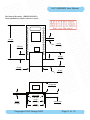
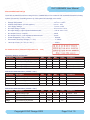
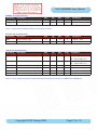
1
WW .100Y.C M.TW
WW .100Y.C M.TW
WW 00Y.CO .TW
WW 00Y.CO .TW
W
W
W
T
.1
W.1 Y.COM W
M.
OM
W
O
W
C
.
W
C
W
Y
W
.T
W
Y.
W
.100
M.T
.100
OM
W
M.T
.100
O
W
C
.
O
W
W
C
W
Y
W
WW .100Y.
.TW
DLP-USB245M
Manual
WW .100Y.C M.TW
M.T
.100 User
M
O
W
O
W
C
.
O
W
WW .100Y
.TW
WW .100Y.C M.TW
WW .100Y.C M.TW
M
O
W
O
W
O
W
WW .100Y.C M.TW
WW .100Y.C M.TW
WW .100Y.C M.TW
O
WW 00Y.CO .TW
W
WW 00Y.CO .TW
C
.
W
W
W
Y
W
W
M
.1
.T
00
W.1 Y.COM W
WW 00Y.CO .TW
W.1 Y.COM W
W
W
W
W
.T
00
W
M
.1
.T
00
W.1 Y.COM W
WW 00Y.CO .TW
W.1 Y.COM W
W
W
W
W
W
M
M.T
.100
W.1 Module
M.T
.100
OParallel
W
.CO .TW
O
W
W
C
.
DLP-USB245M-G
USB
to
FIFO
Interface
Y
W
C
W
.
0
Y
W
W
W
0
0
Y
W
T
.
0
W
M
.T
00 is the
W.1 Y
OM
W.1 version
The DLP-USB245M-G
of DLPWDesign’s USB
adapter.
This
adds
.COdevice
OM 2nd generation, lead-free
W
W.1 Y.C
C
.
W
0
Y
W
W
.TW
W
0
0
W
T
.
1
0
0
W
T
M
.
.
1
0
M
.
O
1
Wa new Y
M
extra functionality
DLP-USB1
predecessor W
with a reduced
and
low
O component count W
.C price..TW
W. to it’s O
W
00
WW .100Y.C M.TW
1
WW .100Y.C M.TW
M
.
W
O
W
.CO .TW
O
W
W
C
.
Y
W
C
W
.
0
Y
W
W
W
DLP-USB245M
0
0
Y
W
.T AREAS
0APPLICATION
W FEATURES
W.1 Y.COM W
M.T
.100
OM
W.1 • YRapid
O
W
W
C
.
W
C
• Send / Receive
Data
over
USB
at
up
to
1
M
Bytes
/
Prototype
Development
W
.
W
.T
W
00
W
WW .100Y
M.T
.100
W.1 Y.COM W
M.T
O
W
O
W
W
C
sec
•
USB
ISDN
and
ADSL
Modems
.
W
W
WW .100Y
WW .100Y.C M.TW
M.T
.100
M.T
O
W
O
• 384 byte FIFO Transmit
buffer
/
128
byte
FIFO
W
C
.
O
W
W
USB
PDA Interface
W
Y
W
0Y.CSpeed
WW • .10High
.TW
0Y.Cthroughput
WWfor high
M.T
.100
.TW
0data
M
O
receive buffer
1
W
M
.
O
W
•
USB
Interface
for
Digital
Cameras
C
W
.CO .TW
WW .100Y.
.TW
WW .100Y.C M.TW
WWto CPU
M
• Simple interface
00orYMCU bus
O
1
W
M
.
O for MP3 players W
Interface
.C
O
W
W
W•W USB
W
W
00Y
0Y.C M.TW
Y.C required
• No in-depth knowledge
as all USB W
1
0
WW .1of
T
M.T
.
.
1
00USB
.
O
•
High
Speed
USB
Instrumentation
W
M
O
W
C
W
.CO .Tthe
WW .100Y.
• Protocol is handled
.TW
Wmodule WW .100Y.C M.TW
WW automatically
M
00Y within
O
1
W
•
USB
Smart
Card
Readers
M
.
W
W drivers
.CO .TW
• FTDI’s Virtual COMWport
the
CO
WW .100Y.C M.TW
W need W•W Set.Top
0Y
Y.eliminate
0
0
W
T
.
1
0
Box
(S.T.B.)
PC-USB
interface
M
1
M
for USB driver development
Ocases.
WW 00Y.CO .TW
W. in most
WW 00Y.CO .TW
C
.
W
W
W
Y
W
W
.T
1
00
• USB
Modems
M
W.1 Y.COM
• Integrated 3.3v Regulator
O
W.Hardware
OMRegulator
W
W–.1No External
C
.
W
C
W
.
Y
W
W
.T
W
M.T
.100
.TW
100 Modems
00Y
Required
• W USBW
Wireless
M
.
O
1
W
M
.
O
C
.
O
W
.C
.C
WW .100Y
.
WW .1Code
.TW
00Y Readers
• Integrated Power-On-Reset
WW circuit
.TW
00Y
• USB Bar
M
OM
1
W
M
.
O
W
C
.
O
W
W
C
.
Y
W
.C PLL.TW
W
• Integrated 6MHz – 48Mhz
WW .100Y
WWclock.1multiplier
.100
00Y
M.T
OM
W
M
O
W
C
.
O
W
W
C
.
Y
W
C
• USB Bulk or Isocronous data
transfer
modes
W
.
0
Y
W
0
W
.T
WW .100Y
.TW
.100
W.1 Y.CO
M
OM
W
O
W
W
• 4.4v - 5.25v Single Supply taken
directly
from
the
C
.
W
C
W
Y
W
W
W
WW .100Y.
.100
M.T
.100
O
W
M.T
O
USB port
W
O
W
W
C
.
Y.C
W
W
.C
0
Y
W
W
W
0
0
Y
W
T
.
1
0
0
W
T
.
.
0
M
.1
• UHCI / OHCI / EHCI host controller .compatible
WW 00Y.C
W 1 Y.COM W
WW 00Y.CO .TW
W
W
W
W
.1
• USB 1.1 and USB 2.0 compatible
.T
00
W.1 Y.COM W
WW 00Y.
W.1 Y.COM W
W
W
W
W
• USB VID, PID, Serial NumberW
and Product
.T
.100
W.1 Y
M.T
.100
OM
W
O
W
W
C
.
W
C
W
Y
Description
W
W
00
W
WW .100Y.
M.T
.100
W.1
M.T
O
W
O
W
W
C
• Strings stored in on-board EEPROM.
.
W
W
WW .100Y
WW .100Y.C M.TW
.100
M.T
W
O
W
• EEPROM programmable on-board via W
USB
O
W
.C
W
WW .100Y.C M.TW
WW for
.1
.TW
00Y
1
• VIRTUAL COM PORT ( VCP ) DRIVERS
M
.
O
W
O
WW
W
C
.
W
C
W
.
Y
W
W
W
W
.T
00
.
.T
00Y
- Windows 98 and Windows 98 SE W
W.1 Y.COM W
WW
W.1 Y.COM W
W
W
W
W
.T
- Windows 2000 / ME / XP
W
.100
W
M.T
.100
OM
W
O
W
C
.
W
C
W
Y
WW
- Windows CE **
W
0
W
T
.
0
WW .100Y.
T
.
1
OM
W.
OM
W
- MAC OS-8 and OS-9
WW .100Y.C M.TW
WW .100Y.C M.TW
O
W
O
W
- MAC OS-X
WW .100Y.C
WW .100Y.C M.TW
W
O
W
- Linux 2.40 and greater
WW
WW .100Y.C M.TW
• D2XX ( USB Direct Drivers + DLL S/W Interface )W
.CO .TW
W
Y
0
W
0
- Windows 98 and Windows 98 SE
M
.1
WW 00Y.CO
W
- Windows 2000 / ME / XP
W.1
W
W
[ ** = In planning or under development ]
Copyright © DLP Design 2002
Page 1 of 15
WW .100Y.C M.TW
WW .100Y.C M.TW
WW 00Y.CO .TW
WW 00Y.CO .TW
W
W
W
T
.1
W.1 Y.COM W
M.
OM
W
O
W
C
.
W
C
W
Y
W
.T
W
Y.
W
.100
M.T
.100
OM
W
M.T
.100
O
W
C
.
O
W
W
C
W
Y
W
WW .100Y.
.TW
DLP-USB245M
Manual
WW .100Y.C M.TW
M.T
.100 User
M
O
W
O
W
C
.
O
W
WW .100Y
.TW
WW .100Y.C M.TW
WW .100Y.C M.TW
M
O
W
O
W
O
W
WW .100Y.C M.TW
WW .100Y.C M.TW
WW .100Y.C M.TW
O
WW 00Y.CO .TW
W DESCRIPTION
WW 00Y.CO .TW
C
GENERAL
.
W
W
W
Y
W
W
M
.1
.T
00
OM
W.1 method
OM
WW 00Y.CO .TW
W.1 Y.Cprovides
C
.
W
The DLP-USB245M
an easy cost-effective
W
Y
W
W
W
W
.T
00
W
00
W.1 Y.COM W
M.T
OM
W.1at upYto
W
W.1 dataY.toCO
C
.
W
of transferring
/
from
a
peripheral
and
a
host
W
W
W
W
.T
W
M.T
.100
.TW
100
00
M
.
O
1
W
M
.
O
W
C
W(1-Megabyte)
.C
.CO per.Tsecond.
8 Million
bits
Its simple
WW .100Y.
.TW
W
WW FIFO-like
.TW
00Y
WW
M
1
00Y
M
.
O
1
W
M
.
O
W
O
design W
makes
to any microcontroller
WW .100Y.C M.TW
WWit easy
W
Yto.Cinterface
WW .1or00Y.C M.TW
0
T
.
0
1
OM
WW 00Y.CO .TW
W.via IO Y
WW 00Y.CO .TW
C
.
W
microprocessor
ports.
W
W
W
W
M
.1
.T
00
W.1 Y.COM W
WW 00Y.CO .TW
W.1 Y.COM W
W
W
W
W
.T
00
W
W.1 Y.COM W
M.T
.100
W.1 Y.COM W
O
W
W
W
C
.
W
W the 0peripheral
To send data
to theW
host computer
.T
00
Y
W
Wfrom
M.T
.100
W.1 Y.COM W
M.T
.1 0
O
W
O
W
W
C
.
W
W
Y
W
simply write the
byte wide0data
module when
W
Y.C into the
WTXE#
WW
M.T
.100
M.T
.100
O
W
M.T
.10
O
W
C
.
O
W
W
.C
is low. If the (384W
storing the
written
W byte, the
.C buffer .fiTllsWup or is busy
Ypreviously
W device.1takes
00Y TXE#M.TW
WW
.T
W byte) .transmit
100
00Y
M
.
O
1
W
M
O
W
O being written until some
W data
.C data.T
Y.Cto the .TW
W of the
Wbeen transferred
.Cfrom
high in order to W
stop
FIFO
has
0USB
Y
WW over
Wfurther
W
0
0
Y
W
1
0
0
T
M
.
.
0
W.1 Y.COM W
WW 00Y.CO .TW
W.1 Y.COM W
W
host.
W
W
W
.T
W
.100
W.1 Y.COM W
M.T
.100
OM
W
O
W
W
C
.
W
C
W
Y
W
.T
W
W
WW .100Y.
.100
M.T
.100
OM
W
M.T
O
W
C
.
O
W
W
C
W
.
Y
Wlet the peripheral
W
W to the00peripheral
When the host sends
over
low.Tto
know
Y.C
WW will.1take
00YRXF# M
Wdata
.100that at OM.T
.TWUSB, the device
1
W
M
.
O
W
C
.
O
W more 0data
W
W
.C
Y
Wdata until
W indicating
Wno
least one byte of dataW
is W
available.
the
Y.Cperipheral
.Thigh
1 0 is OM.T
00YRXF# goes
.
.TWthen readsW
1
00The
M
.
1
W
M
.
O
W
O
W
WW .100Y.C M.T
available to read.
WW .100Y.C M.TW
WW .100Y.C M.TW
O
WW 00Y.CO .
W
WW 00Y.CO .TW
C
.
W
W
W
Y
W
W
M
.1
100
M.T
W.1 Y.COM W
Operipheral
WW 00Y.CO
W.drivers,
W
C
.
W
W
By using FTDI’s virtual COM
Port
the
looks
like
a
standard
COM
Port
to
the
application
software.
W
Y
W
.T
00
W
W.1 Y.COM
M.T
.100
W.1 Y.COM W
O
W
W
W
C
.
W
Ware ignored
Commands to set the baud W
rate
device
data
W
.Trate regardless of the
.100
.TW always transfers
100at its fastest
00Y – theM
M
.
O
1
W
.
O
W
W
.C
W
W DLP Design’s
.CO of.T
Y
WW .100Y.C
W
application’s baud rate setting.
The latest
versions
the
drivers
are
available
for
download
from
0
Y
W
T
.
0
0
WW
1
0
O
W
OM
W.
OM
W.1
WW .100Y.C
website at http://www.dlpdesign.com.
WW .100Y.C M.TW
WW .100Y.C M.TW
W
O
W
O
W
WW .100Y.C
WW .100Y.C M.TW
WW .100Y.C M.TW
W
O
W
O
W
WW .100Y.
WW .100Y.C M.TW
WW .100Y.C M.TW
W
O
W
O
W
WW .100Y
WW .100Y.C M.TW
APPLICATION NOTES
WW .100Y.C M.TW
W
O
W
O
W
WW .100
WW .100Y.C M.TW
WW .100Y.C M.TW
O
O
WW
W
.Cthe
WisW
C
W
.
Y
W
W
0
Y
W
T
USB devices transfer data in packets.W
If W
data is to0be
sent
from
the
PC,
a
packet
built
up
by
application
program
.
0
0
.1
.T
W.1 Y.COM W
WW
W.1 Y.COM W
W
W
W
0 list of tasks
W
.T for the USB
and is sent via the device driver to the USB
puts a request
onto0the
W scheduler.
.
.T
00 This scheduler
W.1 Y.COM W
WW
W.1 Y.COM W
W
W
W
W
host controller to perform. This will typically
up the new
W take at.1least
00 1 millisecond
M.T
.1it00will notOpick
W
M.T to execute because
W
O
W
C
.
W
C
W
Y
WW
W
0
Y.millisecond).
W
T
.
request until the next ‘ USB Frame’ (the frame
is
1
0
0
WWperiod
T
.
1
0
OM
W.
OM
W.1
WW .100Y.C M.TW
WW .100Y.C M.TW
O
W
W
.CO throughput)
Y.C the data from
W
0
Yrequired
WW with
0
0
There is therefore a sizeable overhead (depending
associated
moving
WW on .your
T
.
1
0
.
1
OM
WW
WWat a0time’
W
Y.Cby an application,
W
0
W‘byte
T
the application to the USB device. If data is sent
this
will
severely
limit the overall
M.
.1
O
W
C
.
W
WW .100Y
throughput of the system as a whole.
M.T
O
W
WW .100Y.C
W
WW
It must be stressed that in order to achieve maximum
throughput, application programs should send or receive data
using buffers and not individual characters.
Copyright © DLP Design 2002
Page 2 of 15
WW .100Y.C M.TW
WW .100Y.C M.TW
WW 00Y.CO .TW
WW 00Y.CO .TW
W
W
W
T
.1
W.1 Y.COM W
M.
OM
W
O
W
C
.
W
C
W
Y
W
.T
W
Y.
W
.100
M.T
.100
OM
W
M.T
.100
O
W
C
.
O
W
W
C
W
Y
W
WW .100Y.
.TW
DLP-USB245M
Manual
WW .100Y.C M.TW
M.T
.100 User
M
O
W
O
W
C
.
O
W
WW .100Y
.TW
WW .100Y.C M.TW
WW .100Y.C M.TW
M
O
W
O
W
O
W
WW .100Y.C M.TW
WW .100Y.C M.TW
WW .100Y.C M.TW
O
WW 00Y.CO .TW
W
WW 00Y.CO .TW
C
.
W
W
W
Y
W
W
M
.1
.T
00
W.1 Y.COM W
WW 00Y.CO .TW
W.1 Y.COM W
W
W
W
W
.T
00
W
M
.1
.T
00
DRIVER SOFTWARE
W.1 Y.COM W
WW 00Y.CO .TW
W.1 Y.COM W
W
W
W
W
.T
W
.100
W.1 Y.COM W
M.T
.100
OM
W
O
W
W
C
.
W
C
W
.T
W
W
.TW
00Y
WW .100Y.
.100that they
Mroyalty-free
.1are
OM
W
M.Tdriver executableW
O
FTDI’s VCP W
(Virtual COMOPort)
files
provided
on
the
condition
are
only
W
C
.
W
C
.
W
.TW
00Y
W
.TW
1
00Y
WW .100Y.C M.TW
M
.
1
M
.
O
W
O
used with designs
and DLP-USB245M). The
latest version of the
WFT245BM
O an FTDI device (ieWthe
W incorporating
W
Y.C
WW .100Y.C M.TW
0
W
T
.
0
WW .100Y.C M.TW
1
O
W
OM
drivers can be downloaded
from
W.
O dlpdesign.com or ftdichip.com.
W
WW .100Y.C M.TW
WW .100Y.C M.TW
WW .100Y.C M.TW
O
WW 00Y.CO .TW
W
WW 00Y.CO .TW
C
.
W
W
W
Y
W
W
M
.T
00
M Windows ME and W
.1WindowsO‘98,
W.1 2000/XP.
W
The VCP driver download
isOaM
combined set of drivers
for
Windows
.CO .TW
W.1 file
C
.
Y
W
C
W
.
0
Y
W
W
W
0
W
.T
00
0Y
W
.T
OM
W.1 diskYor.Cfolder
M
.10floppy
OM
W.1drivers
Unzip the file to a blank
disk
or folder on your PC.WThe
can
co-exist on the sameW
floppy
O
W
C
W
.
C
W
.
0
Y
W
W
.T
00
WW .100Y
M.T
.10
.TW
1
M
.
O
W
M
O
W
C
since the INF files determine
which
each operating system version. Once
the
Oset of drivers to load for
W
Y. VCP .TW
WWloaded,
WW .100Y.C M.TW
100
WW .100Y.C M.TW
M
.
W
O with the DLP-USB245M
Wto communicate
drivers allow your application
software,
PC,
as though
.CO it .TW
O running on the hostW
W
W
C
.
Y
C
W
.
0
Y
W
W
W
0
Y
W
.T
W
.100
100
W.1 Y.COM W
M.T
.(RS-232)
OM
W
were connected to a COM
port.
O
W
W
C
.
W
C
W
Y
W
.T
W
W
WW .100Y.
.100
M.T
.100
OM
W
M.T
O
W
C
.
O
W
W
C
W
Y
W
WW .100Y.
.TW
WW .100Y.C M.TW
M.T
.100
M
O
W
O
W
C
.
In addition to VCP drivers,
FTDI’s “D2XXODirect Drivers” for Windows
offer an alternative solution toW
theWVCP drivers
W
Y
.TW
WW .100Y.C M.TW
100
WW .100Y.C M.TW
M
.
O
W
O
W using a DLL instead of a Virtual Com
O with the FT245BM device
that allows application software
The
W to interface
Y.C
WW Port.
WW .100Y.C M.TW
100
WW .100Y.C M.TW
M.T
.
O
W
O
W
C
.
O
W consists of a Windows WDM driver
architecture of the D2XX drivers
with the FT245BM
viaY
Y.C
WWdevice
.
WWthat .communicates
.TW
WW .100Y.C M.TW
.100
100
M
OM
W
O
W
C
.
O
W
C
the Windows USB Stack andW
aW
DLL that interfaces
the
Application
Software
(written
in
VC++,
C++
Builder,
Delphi,
.
Y
W
.C
W
WW .100Y
W
.100
.TW
00Y
M.T
OM
1
W
M
.
O
W
C
.
O
W
W
C
VB etc...) to the WDM driver. An
INF
installation
file,
uninstaller
program
and
D2XX
programmers
guide
complete
the
.
Y
W
C
W
.
0
Y
W
W
0
W
.T
WW .100Y
.100
W.1 Y.CO
M.T
OM
W
O
W
W
C
package
.
W
C
W
Y
W
W
W
WW .100Y.
.100
M.T
.100
O
W
M.T
O
W
O
W
W
C
Y.C
W
0
W
0
WW .100Y.
T
.
1
WW .100Y.C M.TW
M
W.
O access and controlWofWmultipleYFT245BM
W
The D2XX Direct Drivers add support
for simultaneous
The WW
.CO .Tdevices.
C
W
.
0Y.C
W
W
0
0
Y
W
1
0
0
W
T
.
.
1
0
W
.1
OM
W. Product
OM to be opened either
W
Extended Open function (FT_OpenEx
) allows the device
W or by Serial
Y.C Description
WW .100Y.
0
WW by it’s
T
.
0
WW .100Y.C M.TW
M
.1
W
O The List Devices function
W to beYunique.
.CO .TW
Number, both of which can be programmed
allows the WW
Y
WW (FT-ListDevices)
C
.
Y
W
W
0
W
100
0
0
W
T
.
.
1
0
M
.
1
W
M
.
O
W
O
W
W
application software to determine whichW
devices
are
currently
available
for use,
Y.C description
W
0product
Y.C
WWagain.1by
TW or by W
.
0
0
W
T
.100
.
0
M
1
W
M
.
O
W
O
W
W
serial number.
W
WW .100Y.C M.TW
WW .100Y.C M.TW
.1
O
W
O
WW
W
C
.
W
C
W
.
Y
W
W
W
Y
W
.T
00
W
.T
100
W.
OM the
W.1 Y
OM
W
W.to
C
.
W
C
Several new features have been recently added
the Y
D2XX
drivers.
Functions
are
provided
to
program
W
.
W
W
W
W
W
M.T
.100
W
M.T
.100
O
W
O
W
C
.
W
C
EEPROM (FT_EE_Program), and read the EEPROM
EEPROM
is called
W the
Y
WW
WUnused space
0
W in the
T
.
0
0Y.
WW .10(FT_EE_Read).
T
.
1
M
W.
OM FT_EE_UASize W
W
CO
.FT_EE_UAWrite
User Area (EEUA), and functions are providedW
the
gets its size,
.CEEUA.
Y
W
0
Y
W
.TW
0
0
W to access
T
.
1
0
M
.
1
M
.
O
W
W
writes data into it, and FT_EE_UARead is used W
contents.
.CO .TW
WW .100Y.C
W to read.1its
00Y
M
W
O
W
WW
WW .100Y.C M.TW
O
W
Download FTDI Application Notes AN232-03, AN232-05,
for detailed instructions on how to
W
Y.C and.AN232-07
0
WW AN232-06,
0
MT
.1
O
W
install and remove the drivers.
WW .100Y.C
W
WW
Copyright © DLP Design 2002
Page 3 of 15
WW .100Y.C M.TW
WW .100Y.C M.TW
WW 00Y.CO .TW
WW 00Y.CO .TW
W
W
W
T
.1
W.1 Y.COM W
M.
OM
W
O
W
C
.
W
C
W
Y
W
.T
W
Y.
W
.100
M.T
.100
OM
W
M.T
.100
O
W
C
.
O
W
W
C
W
Y
W
WW .100Y.
.TW
DLP-USB245M
Manual
WW .100Y.C M.TW
M.T
.100 User
M
O
W
O
W
C
.
O
W
WW .100Y
.TW
WW .100Y.C M.TW
WW .100Y.C M.TW
M
O
W
O
W
O
W
WW .100Y.C M.TW
WW .100Y.C M.TW
WW .100Y.C M.TW
O
WW 00Y.CO .TW
W
WW 00Y.CO .TW
C
.
W
W
W
Y
W
W
M
.1
.T
00
W.1 Y.COM W
WW 00Y.CO .TW
W.1 Y.COM W
W
W
W
W
.T
00
W
.T
W.1 Y.COM W
.100 UTILITY
W.1 Y.COM W
EEPROMW
WRITE
OM
W
W
C
.
W
W
W
.T
W
M.T
.100
.TW
100
00Y
M
.
O
1
W
M
.
O
W
C
O
W
WW .100Y.
.TW
WW .100Y.C M.TW
WW .100Y.C M.TW
M
O
W
O information that is written
W
O option to accept manufacturer-specific
The DLP-USB245M
has the
the.C
93C46 TW
W
WW into
.
00Y
WW .100Y.C M.TW
1
WW .100Y.C M.TW
.
OMproduct
W
O the PID identifiers, W
W
C
.
O
EEPROM. W
Parameters
that
can
be
programmed
include
the
VID
and
the
manufacturer’s
W
C
.
Y
W
C
.
W
.TW
W
.TW
100
00Y
W
M
.
.TW
1
00Y
M
.
O
1
W
M
.
O
W
O
string and a W
serial
W number.
WW .100Y.C M.TW
W
Y.C
WW .100Y.C M.TW
0
W
T
.
0
1
OM
WW 00Y.CO .TW
W.
WW 00Y.CO .TW
C
.
W
W
W
Y
W
W
.1
.T
OM
.100EEPROM
OM
W.1 for the
.Cbased
OMserializer and testingWutility
WWthe 0VCP
W
C
FTD2XXST is the
latest
FT245BM
device. It replaces
.
Y
C
W
.
0
Y
W
W
.TW
W
W
.T
1
00
W
M
.
.T
1
00Y
M
.
O
1
W
M
.
O on Win ‘98, Win ME
W
.C
O on the new D2XX drivers
W
232Prog utility. FTD2XXST
is based
will
2000/
W
.Cwork
WWand .Win
00Y
WW .and
.TW
1
00Y
WW .100Y.C M.TW
M.T
1
M
O
W
O
W
C
W installYthe
XP platforms. YouW
must
D2XX
in.Corder to run
this application.
to
Y.the
W drivers
.COlatest.Trelease
WW Refer
.TW
W of theW
.TW
100
00Y
W
M
.
1
00
M
.
O
1
W
M
.
O file for details on how
W
.C
O
Wis included
SER200.PDF guideW
that
EEPROM
Write Utility’s
the
W
WW to .use
W
00Y
0Y.C zip
Y.C in the.T
WW .1download
TW
.
1
0
0
W
M.T
0
M
O
1
W
M
.
O
W
C
O
W
serializer.
WW .100Y.
.TW
WW .100Y.C M.TW
WW .100Y.C M.TW
M
O
W
O
W
O
W
WW .100Y.C M.TW
WW .100Y.C M.TW
WW .100Y.C M.TW
W
.CO .TW
O
WW these
W onYthe
.CO process
Y
If you have VCP drivers W
installed
PC that W
is to performW
the
write
you must W
uninstall
WEEPROM
C
W
.
0
Y
0
0
T
W
.T
00
M.
.10
W.1 Y.COM
OD2XX
W
OM with the driver files)
W
W.1 Y
C
.
W
drivers using the uninstaller
program
(included
and
install
the
drivers
prior
to
running
the
C
W
.
Y
W
W
W
.T
W
M.T
.100
.TW
100
00
M
.
O
1
W
M
.
O
W
C
.
O
W
serializer utility.
WW .100Y
.
WW .100Y.C M.TW
WW .100Y.C M.TW
OM
W
O
W
C
.
O
W
W
C
.
Y
W
W
WW .100Y
WW .100Y.C M.TW
.100
M.T
OM
W
O
W
C
.
O
W
W
C
.
Y
W
C
QUICK START GUIDE
W
.
0
Y
W
W
0
W
.T
WW .100Y
.100
W.1 Y.CO
M.T
OM
W
O
W
W
C
.
W
C
W
Y
W
W
WW .100Y.
.100
.TW
M.T
.100
O
W
M
O
W
O
W
W
C
This guide requires the use of a Windows
98/2000
PC
that
is
equipped
with
a
USB
port.
Y.C
W
0
W
0
WW .100Y.
T
.
1
WW .100Y.C M.TW
.
M
O
WW 00Y.C
W
WW 00Y.CO .TW
C
.
W
W
W
Y
W
W
00
W.1 Y.
M.Teither dlpdesign.com
OM Unzip the drivers onto
Wor.1ftdichip.com.
1. Download the DLL version of the device
Ofrom
W
W.1 drivers
C
.
W
C
W
.
Y
W
W
W
W
0Y
W
.100
M.T
.100
W
M.T
.10hard
O
W
a blank floppy disk or into a folder onWthe
drive.
O
WW .100Y
WW .100Y.C M.TW
WW .100Y.C M.TW
W
O
W
WW .100
WW 00Y.CO .TW
WW .100Y.C M.TW
W
2. Download the serializer program from either
Unzip
place it in a WW
W the package
OM or ftdichip.com.W
W.1 dlpdesign.com
.CO and
C
W
.
Y
W
W
W
0
Y
W
T
.
W
.1
M
.10
folder on the hard drive.
M.T
.100
O
W
O
WW
W
C
.
W
C
W
.
Y
W
W
W
W
.T
00
W
.
.T
00Y
W.1 Y.COM W
WW
W.1 Y.COM W
W
W
W
W sure
.T
W
3. Select a power source for the DLP-USB245M
RESET#
pin
.10to0 pull the
100 viaOpins
W
M.T10, 11, and 12. Be
.module
OM
W
W
C
.
W
C
W
.
Y
WW
W
W
0
Y
W
T
.
0
0
W
T
.
1
0
high (pin 3).
OM
W.
OM
W.1
WW .100Y.C M.TW
WW .100Y.C M.TW
WW 00Y.CO
WW 00Y.CO .TW
W
W
4. Connect the DLP-USB245M board to the PC via a.1
6-foot
action
M USB cable. ThisW
W.1 initiates the loading
O
W standard,
C
.
W
W
0Y theM
Wthe folder
.TW
of the USB drivers. When prompted, select
DLL
version of the device drivers were stored
.10where
O
W
C
.
W
WW .100Y
M.T
O
W
WW .100Y.C
W
WW
Copyright © DLP Design 2002
Page 4 of 15
WW .100Y.C M.TW
WW .100Y.C M.TW
WW 00Y.CO .TW
WW 00Y.CO .TW
W
W
W
T
.1
W.1 Y.COM W
M.
OM
W
O
W
C
.
W
C
W
Y
W
.T
W
Y.
W
.100
M.T
.100
OM
W
M.T
.100
O
W
C
.
O
W
W
C
W
Y
W
WW .100Y.
.TW
DLP-USB245M
Manual
WW .100Y.C M.TW
M.T
.100 User
M
O
W
O
W
C
.
O
W
WW .100Y
.TW
WW .100Y.C M.TW
WW .100Y.C M.TW
M
O
W
O
W
O
W
WW .100Y.C M.TW
WW .100Y.C M.TW
WW .100Y.C M.TW
O
WW 00Y.CO .TW
W
WW 00Y.CO .TW
C
.
W
W
W
Y
W
1
W in step.1one.
installation of the device drivers for the
M board. The
.DLP-USB245M
.Twill then complete the
00 Windows
W.1 Y.COM W
OM
WW 00Y.CO .TW
W
W
C
.
W
W
W
00the host PC.T
0YDLP-USB245M
Wnext time
module W
is attached,
will immediately loadW
the
M without any
.1 correct drivers
.T
0the
W.1 Y.COM W
.CO .TW
W
W.1 Y.COM W
Y
W
0
W
W
0
.T
0
W
prompting.
the
to do so..100
.T if promptedW
W.1 Y.COM W
MPC
.10Reboot
OM
W
O
W
W
C
.
W
C
W
Y
W
.T
W
W
WW .100Y.
.100
M.T
.100
OM
W
M.T
O
W
C
.
O
W
W
C
W
W
.C
0Y
W of your
W serializer
0Y.(6001),Ma.Tdescription
WW
5. Run
(0403),10
PID
string
and
Wthe
TWwrite the VID
M.T
.10choosing
.and
00Yprogram
.
O
1
W
M
.
O
W
C
.
O
W
W
Y
Y.Cwas downloaded
.TW
Y.Cinstructed
WW manual
manufacturers
in the instruction
withW
the serializer
.TW
100 software.
00that
WW .1ID
M
.
.TW
1
00as
M
.
O
W
M
O
W
O
W
W
Y.C 10 seconds
.TW
W
00Wait
0Y.C Mboard
Y.C program
WWthe DLP-USB245M
TW from theW
Terminate
and disconnect
USB cable.
.
1
0
0
WWthe serializer
T
M
.
.
1
0
.
O
1
W
O
W
OM
W.
W so.
Y.C
WW .100Y.C M.TW
W
Y.C
WWthe PC
Tdo
and reconnect
DLP-USB245M
board. Reboot
if0instructed
to
.
0
0
WW the
T
.
1
0
M
.
O
W
O
W
OM
W.1
WW .100Y.C M.TW
WW .100Y.C M.TW
WW .100Y.C M.TW
O
WW 00Y.CO .TW
.CO .TW
WWa default
Y
W
WW 00Y.C
W
0
W
NOTE 1 - TheW
DLP-USB245M
comes
pre-programmed
with
VID
and
PID.
Step
5
is
optional
M
M
.10
W.1and only
M.T
.1
O
W
.CO .TW
O
W
W
C
.
Y
W
C
W
.
0
Y
W
W
W
0
0
Y
W
.T
required if different
0
W VID/PID
M
.1
.T
00codes are required.
W.1 Y.COM W
WW 00Y.CO .TW
W.1 Y.COM W
W
W
W
W
NOTE 2 – The “Test”
the.TDLP-USB232M module.1(and
W button
M
100use with
.for
M.T program is intended
.10on0 the serializer
OM
W
O
WW 00Y.CO .TW
W
C
.
W
C
W
.
Y
W
W
W
0
Y
W
T
.
0 if used with
FT232BM device)
TheM
“Read”
function will work
and
W and will
M
.1 will
.T the DLP-USB245MWmodule.
0fail
.10
O
WW 00Y.CO .TW
W.1 Y.COM W
C
.
W
W
Y
W
W
0 description
W number
.T
0
W of the
present the contents
as.T
well as the serial
M
.1
.10and
WEEPROM.
M
.10EEPROM
OM strings stored inWthe
W
.CO .TW
O
W
C
.
Y
W
C
W
.
0
Y
W
W
W
0
0
Y
W
T
.
0
W
M
.1
.T
00
W.1 Y.COM W
WW 00Y.CO .T
W.1 Y.COM W
W
W
W
W
00
0 for use.
W
At this point the DLP-USB245M
ifW
data
.1 sent OM
M.T non-responsive
M.TNote that the DLP-USB245M
.is10ready
Oappear
W.1 Y.will
.C
O
W
W
C
W
C
W
.
W
.
W by an attached
00Y
0
Y
W
T
.
1
0
0
WWfrom .the
T
.
from the host PC is not read
FT245BM
device
microcontroller/microprocessor/DSP/FPGA/
.
1
0
M
.
OM
1
W
M
O
W
C
.
O
W
W
C
.
Y
W
W
WW .100Y
WW .100Y.C M.TW
.100
etc…
M.T
OM
W
O
W
C
.
O
W
W
C
.
Y
W
C
W
.
0
Y
W
W
0
W
.T
WW .100Y
.100
W.1 Y.CO
M.T
OM
W
O
W
W
C
.
W
C
W
Y
W
W
W
WW .100Y.
.100
M.T
.100
O
W
M.T
O
W
O
W
W
C
Y.C
W
0
W
0
WW .100Y.
T
.
1
WW .100Y.C M.TW
.
M
O
WW 00Y.C
W
WW 00Y.CO .TW
C
.
W
W
W
Y
W
W
.1
.T
00
W.1 Y.COM W
WW 00Y.
W.1 Y.COM W
W
W
W
W
.T
W
.100
W.1 Y
M.T
.100
OM
W
O
W
W
C
.
W
C
W
Y
W
W
00
W
WW .100Y.
M.T
.100
W.1
M.T
O
W
O
W
W
C
.
W
WW .100Y
.TW
WW .100Y.C M.TW
.100
M
W
O
W
O
W
W
W
WW .100Y.C M.TW
WW .100Y.C M.TW
.1
O
W
O
WW
W
C
.
W
C
W
.
Y
W
W
W
W
.T
00
W
.
.T
00Y
W.1 Y.COM W
WW
W.1 Y.COM W
W
W
W
W
.T
W
.100
W
M.T
.100
OM
W
O
W
C
.
W
C
W
Y
WW
W
0
W
T
.
0
WW .100Y.
T
.
1
OM
W.
OM
W
WW .100Y.C M.TW
WW .100Y.C M.TW
O
W
O
W
WW .100Y.C
WW .100Y.C M.TW
W
O
W
WW
WW .100Y.C M.TW
O
W
WW .100Y.C M.TW
O
W
WW .100Y.C
W
WW
Copyright © DLP Design 2002
Page 5 of 15
WW .100Y.C M.TW
WW .100Y.C M.TW
WW 00Y.CO .TW
WW 00Y.CO .TW
W
W
W
T
.1
W.1 Y.COM W
M.
OM
W
O
W
C
.
W
C
W
Y
W
.T
W
Y.
W
.100
M.T
.100
OM
W
M.T
.100
O
W
C
.
O
W
W
C
W
Y
W
WW .100Y.
.TW
DLP-USB245M
Manual
WW .100Y.C M.TW
M.T
.100 User
M
O
W
O
W
C
.
O
W
WW .100Y
.TW
WW .100Y.C M.TW
WW .100Y.C M.TW
M
O
W
O
W
O
W
WW .100Y.C M.TW
WW .100Y.C M.TW
WW .100Y.C M.TW
Table W
1 - DLP-USB245M
PINOUT DESCRIPTION
O
WW 00Y.CO .TW
WW 00Y.CO .TW
C
.
W
W
W
Y
W
W
M
.1
.T
00
W.1 Y.COM W
WW 00Y.CO .TW
W.1 Y.COM W
W
W
W
W
.T
00
W
M
.1
.T
00
W.1 Y.COM W
WW 00Y.CO .TW
W.1 Y.COM W
W
W
W
W
.T
W
.100
W.1 Y.COM W
M.T
.100
OM
W
O
W
W
C
.
W
C
W
Y
W
.T
W
W
WW .100Y.
.100
M.T
.100
OM
W
M.T
O
W
C
.
O
W
W
C
W
Y
W
WW .100Y.
.TW
WW .100Y.C M.TW
M.T
.100
M
O
W
O
W
C
.
O
W
WW .100Y
.TW
WW .100Y.C M.TW
WW .100Y.C M.TW
M
O
W
O
W
O
W
WW .100Y.C M.TW
WW .100Y.C M.TW
WW .100Y.C M.TW
O
WW 00Y.CO .TW
W
WW 00Y.CO .TW
C
.
W
W
W
Y
W
W
M
.1
.T
00
W.1 Y.COM W
WW 00Y.CO .TW
W.1 Y.COM W
W
W
W
W
.T
00
W
W.1 Y.COM W
M.T
.100
W.1 Y.COM W
O
W
W
W
C
.
W
.T
W
.T
WW .100Y
.100
.TW
100
M
.
OM
W
M
O
W
C
.
O
W
W
C
.
Y
W
W
.TW
W
.TW
100
00Y
WW .100Y.C M.TW
M
.
1
M
.
O
W
O
W
O
W
WW .100Y.C M.TW
WW .100Y.C M.TW
WW .100Y.C M.TW
O
W
O
W
O
W
WW .100Y.C M.TW
WW .100Y.C M.TW
WW .100Y.C M.TW
O
W
O
W
O
W
WW .100Y.C M.TW
WW .100Y.C M.TW
WW .100Y.C M.TW
O
WW 00Y.CO .TW
W
WW 00Y.CO .TW
C
.
W
W
W
Y
W
W
M
.1
.T
00
W.1 Y.COM W
WW 00Y.CO .T
W.1 Y.COM W
W
W
W
W
.T
00
W
W.1 Y.COM
M.T
.100
W.1 Y.COM W
O
W
W
W
C
.
W
.
W
00
W
WW .100Y
M.T
.100
W.1 Y.COM
M.T
O
W
O
W
W
C
.
W
W
WW .100Y
WW .100Y.C M.TW
.100
M.T
OM
W
O
W
C
.
O
W
W
C
.
Y
W
Pin#
Description
C
W
.
0
Y
W
W
.T
10
00
WW .100Y
.TW
.1DLP-USB232M.
O
M
OM High for DLP- WW.
W
O
1
BOARD ID (Out) Identifies
the
board
as
either
a
DLP-USB245M
or
W
C
.
W
C
W
.
0Y.C
Y
W
W
W
0
0
Y
W
T
.
1
0
0
W
T
.
.
1
M
.
O
W
M
.10
USB232M and low for DLP-USB245M.
WW 00Y.CO .TW
WW .100Y.C
WW 00Y.CO .TW
W
W
M
.1
2
Ground
W
W.1 Y.COM W
WW 00Y.CO .TW
WW .100Y.C
W
W
W by an.1external
T
3
RESET# (In) Can be used
device
to
reset
the
FT245BM.
If
not
required
this
pin
must
.
1
00
M
.
M
WW 00Y.
W
WW 00Y.CO .TW
.CO .TW
W
W
Y
W
0
W
be tied to VCC.
.1
W.1 Y
M
.10
OM
W
O
W
W
C
.
W
C
W
Y
W
Winternal
W Stays high
00
Y. Generator.
W impedance
4
RESETO# (Out) Output ofWthe
Reset
M.Tafter
.100 for ~O2ms
W.1
M.T
.100
W
O
W
W
C
.
W 3.3v00output
W
Y of the.Tinternal
W
W starts
Y.Cthen clamps
VCC > 3.5v and the internalWclock
.100
.TW it’s outputWto theW
1
00up,
M
.
1
W
M
.
O
O
W
W
W
.C
W
WW
0Y.C Mis.TNOT
regulator. Taking RESET# low
also1force
to go high W
impedance.
Wwill
.1
.TW
10RSTOUT#
00Y RSTOUT#
.
M
.
O
W
O
WW
W
C
.
W
C
W
.
Y
W
W
W
Y
W
.T
affected by a USB Bus Reset.W
00
.T
W.
.100
W.1 Y.COM W
OM
W
W
W
C
.
W
W
5
Ground
W
Y
W
W
M.T
.100
W
M.T
.100
O
W
O
W
C
.
W
C
6
3V3OUT (Out) Output from the integrated
It’s primary purpose
is to0provide
the.TW
Y
WW
W
Y. regulator.
W
0
0
WW .L.D.O.
T
.
1
0
.
OM
OMRSTOUT# pin. A small
W 1 and
WW
internal 3.3v supply to the USB transceiver
amount
of.C
current .TW
.Cthe
Y
W
0
Y
W
0
0
WW .cell
T
0
M
.1
M.
O3.3v
W 1 external
WW 00Y.CO
C
.
(<= 5mA ) can be drawn from this pin
to
power
logic
if
required.
W
W
Y
W
W
.T
00
W.1
W.1 Y.COM W
7
Ground
W
W
W
W
M.T then high during USB suspend.
.100 viaOUSB,
8
SLEEP (Out) Goes Low after the device is configured
W
C
.
W
WW .100Y
M.T Logic Level
Can be used to control power to external logicW
using a P-Channel
O
WW .100Y.C
MOSFET switch.
W
WW
1
24
12
13
Copyright © DLP Design 2002
Page 6 of 15
WW .100Y.C M.TW
WW .100Y.C M.TW
WW 00Y.CO .TW
WW 00Y.CO .TW
W
W
W
T
.1
W.1 Y.COM W
M.
OM
W
O
W
C
.
W
C
W
Y
W
.T
W
Y.
W
.100
M.T
.100
OM
W
M.T
.100
O
W
C
.
O
W
W
C
W
Y
W
WW .100Y.
.TW
DLP-USB245M
Manual
WW .100Y.C M.TW
M.T
.100 User
M
O
W
O
W
C
.
O
W
WW .100Y
.TW
WW .100Y.C M.TW
WW .100Y.C M.TW
M
O
W
O
W in USB
O (In) If the DLP-USB245M
W on this00pin
9 W SND/WUP
a positive W
edge
(WAKEUP)
.C suspend,
Y.C
.TW
WW is
.TW
1
00Y
WW .100Y.C M.TW
M
.
1
M
.
O
W
W
.C
W initiates aOremote wakeup sequence.
device
(not in suspend)
W
.CO is active
WW a .positive
.Tthis
00Y edgeMon
WW If.the
.TW
1
00Y
WW .100Y.C M.TW
1
M
O
W
O
W
C
.
Wpin (SEND)Ocauses the data in theWwrite buffer
theWnext USB
request
.toCbe sent.TtoWthe PC onW
YData-In
.TW
W
100
00Y
WW .100Y.C M.TW
M
.
1
M
.
O
W
W buffer.Y.CO
Ohow many bytes are inWthe
W
regardless of
WW .100Y.C M.TW
W
.TW
00
WW .100Y.C M.TW
1
M
.
W 18..25.
O
Wthe UART interface
10
VCC-IO
(In) 3.0
to
pins 10..12, 14..16
.CO .TW
O volt to +5.25 volt VCC
W
WW and
00Y
WW .100Y.C M.TW
1
WW .100Y.C M.TW
.
OM
W external
O to the 3.3v supply of
W
When
connect Y
VCC-IO
the
.Clogic,
O with 3.3v external logic
W
W interfacing
C
W
.
Y
W
C
W
.
0
W
W
W
.T
W
M.T
.10
.TW
100
00Y
M
.
O
1
W
M
.
O
W
C
.
otherwise
connect
O to VCC to drive out atW5v CMOSYlevel.
W
.C This.Tpin
Wmust be connected
0Y fromM.TW
WW .1to0VCC
W
00
WW .100Y.C M.TW
1
M
.
O
W
O
W
O or EXTVCC.
the target
W electronics
WW .100Y.C M.TW
WW .100Y.C M.TW
WW .100Y.C M.TW
O
WW 00Y.CO .TW
W
WW 00Y.CO .TW
C
.
W
W
W
Y
W
W
M
.1
.T
1 5.25 Volts)
00
OMto the module. Connect
11
EXTVCC
for
applying main powerW
(4.4
W.to
OM
WWto 00Y.CO .TW
W–.1(In) Use
C
.
C
W
.
Y
W
W
W
.T
W
.T powered byW
100 (typical
00Y is to
PORTVCC
the USB
configuration)
W.1 Y.COM W
Mbe
.if1module
OM
W.port
O
W
W
C
.
W
C
W
.
0
Y
W
.T
W
.T is to be powered
00
WW - .(Out)
.10the
.TW
12
PORTVCC
from
USB port. Connect
to
ifM
module
by
1EXTVCC
00YPower M
.
OM
1
W
O
W
C
.
O
W
W
C
.
Y
W
W adapterW
W(typical0configuration).
.TW
W current
USB W
port
500mA maximum
available
to
and target
.TUSB
100
00Y
0Y.C M.TW
M
.
1
M
.
O
1
W
.
O
W device
WW 00Y.CO .TW
WW .100Y.C M.TW
electronics
W for highWpower.
Y.C is configured
0
WWif USB
T
.
1
0
M
.
O
M
.1
O
W FIFO’s
WW
W
13
RXF# - (Out)
When low, atO
least 1 byte is present
in the
128-byte
receive
and
is ready
W bufferW
0Y.C M.TW
Y.C
0
0
WW
T
.
1
0
WW .100Y.C M.TW
.
1
.
O
W
OM
W
WWbuffer
to be read with
RD#. RXF# O
goes high when the W
receive
is.C
empty.
W
Y
WW .100Y.C M.TW
0
T
.
0
WW .100Y.C M.TW
M
.1
O 385 byte transmit buffer
14
WW 00Y.CO .TW
W the FIFO’s
TXE# - WhenW
high,
is full, orYbusy
the last byte
written.
.CO storing
WW
C
W
.
W
W
0
Y
W
T
.
0
0
W
.T
W.1 Y.COM
Mtransmit
.10data
OM
W.1 is high.
O
W
C
Do not attempt W
to W
write
to
the
buffer
when
TXE#
.
W
C
W
.
Y
W
W
W
.T
W
M.T
.100
1800data lines
00aYhigh toMa.T
M
.
O
1
W
.
O
W
C
15
WR (In) When taken
from
low
state,
WR
reads
the
and
writes
the
byte
into
.
O
W
WW .100Y
.
WW .100Y.C M.TW
WW .100Y.C M.TW
OM
W
O
W
C
the FIFO’s transmit buffer.
Data.Cwritten
to the transmit buffer
is
sent
to
the
host
PC
within
the
TX
.
O
W
W
C
.
Y
W
W
WW .100Y
.TW
WW .100Y
.100
Mby
OM
W
M.Tplaced in the RS-232
O
W
C
buffer timeout value ( default
16mS
)
and
buffer
opened
the
application
.
O
W
W
C
.
Y
W
C
W
.
0
Y
W
W
0
W
.T
WW .100Y
.1to00be reprogrammed
W.1 Y.CO
M.T
OM
W
program. Note : The FT245BM
allows
the
TX
buffer
timeout
value
to
a
value
O
W
W
C
.
W
C
Y
W
W
.TW
WW .100Y.
.100
.TW
M
.100the SND
O
W
Mapplicaton
O
W
between 1 and 255mSW
depending
on
the
requirement,
also
pin
can
be
used
to
O
W
W
C
.
Y.C
W
W
.C
0
Y
W
W
0
0
Y
W
T
.
1
0
0
W
T
.
M
.1
M.
.10TX bufferOregardless
send any remaining dataW
inW
the
of the timeout
WW 00Y.C
.CO .TW
WWvalue.
C
.
Y
W
W
0
Y
W
0
W
.T
00
W.1 Y.
16
RD# (In) When pulled low, RD#
data lines from a highWimpedance
OMto the current
W.1 Y.state
O8M
W
W.1takesYthe
C
C
W
.
W
W
.T
W buffer..1Taking
.100
.TWreturns theW
1to00a high O
00
M
.
byte in the FIFO’s receive
RD#Mhigh
data pins
impedance
state
W
W
O
W
.C
W
.C FIFO
WW .100Y
WW
and prepares the next byte
(if available)
.TWto be read.W W.100Y OM.TW
00Y in theM
1
W
.
O
W
WW .100
WBit
W
WW .100Y.C M.TW
17
D7 I/O Bi-directional DataW
Bus
# 700Y.C
T
.
WW
W#.16 Y.COM W
WW 00Y.CO .TW
W
W
18
D6 I/O Bi-directional Data Bus
Bit
W
W
.1
.T
.100
W.1 Y.COM W
OM
WW
W
19
D5 I/O Bi-directional Data Bus Bit
#5
W
C
.
W
W
W
W
.T
00
W
.T
00Y
W.
W.1 Y.COM W
OM
20
D4 I/O Bi-directional Data Bus BitW
#W
4 .1
W
W
C
.
W
W
W
.T
0Y
W
.100
W
M.T
21
D3 I/O Bi-directional Data Bus Bit # 3W.10
OM
W
O
C
.
W
C
W
.
Y
WW
W
W
0
Y
W
T
.
0
0
W
T
.
1
0
M
.
22
D2 I/O Bi-directional Data Bus Bit # 2
W.1 Y.COM W
WW 00Y.CO .TW
W
W
0
W
T
.
23
D1 I/O Bi-directional Data Bus Bit # 1
0
W.1 Y.COM
W.1 Y.COM W
W
W
W
24
D0 I/O Bi-directional Data Bus Bit #W0
.100
M.T
.100
W
O
W
WW
WW .100Y.C M.TW
O
W
WW .100Y.C M.TW
O
W
WW .100Y.C
W
WW
Copyright © DLP Design 2002
Page 7 of 15
WW .100Y.C M.TW
WW .100Y.C M.TW
WW 00Y.CO .TW
WW 00Y.CO .TW
W
W
W
T
.1
W.1 Y.COM W
M.
OM
W
O
W
C
.
W
C
W
Y
W
.T
W
Y.
W
.100
M.T
.100
OM
W
M.T
.100
O
W
C
.
O
W
W
C
W
Y
W
Y.
W
.TW
DLP-USB245M
Manual
0Y.C M.TWExamplesW
WW
M.T
.100 User
Device
100
0Configuration
M
.
O
1
W
.
O
W
C
.
O
W
WW .100Y
.TW
WW .100Y.C M.TW
WW .100Y.C M.TW
M
O
W
O
W
O
W
WW .100Y.C M.TW
WW .100Y.C M.TWMicrocontroller
WW .100Y.C M.TW
O DLP-USB245MWW
WW 00Y.CO .TW
W
.CO .TW
C
.
Y
W
W
W
0
Y
W
0
W
M
.1
.T
00
W.1 Y.COM W
WW 00Y.CO .TW
W.1 Y.COM W
W
W
W
W
.T
00 8
W
M
.1
.T
00
W.1 Y.COM W
WW 00Y.CO .TW
W.1 Y.COM W
W
W
W
W
.T
W
.100
W.1 Y.COM W
M.T
.100
OM
W
O
W
W
C
.
W
C
W
W
.T
W
0Y
W
WW .100Y.
.100
M.T
.10data
OM
W
M.T
O
W
C
.
O
W
W
C
W
Y
W
WW .100Y.
.TW
WW .100Y.C M.TW
M.T
.100
M
O
W
O
WR
W
C
.
O
W
WW .100Y
.TW
Y.C
WW .100Y.C M.TW
WW USB
M
.TW
00'B'
O
1
W
M
.
O
W
O
W
Connector
WW .100Y.C M.TW
W
Y.C
WWRD#.100Y.C M.TW
0
WW
T
.
0
1
OM
WW 00Y.CO .TW
W.
WW 00Y.CO .TW
C
.
TXE#
W
W
W
Y
W
W
M
.1
.T
00
W.1 Y.COM W
WW 00Y.CO .TW
W.1 Y.COM W
W
W
W
RXF#
W
.T
00
W
W.1 Y.COM W
M.T
.100
W.1 Y.COM W
O
W
W
W
C
.
W
.T
W
.T
WW .100Y
.100
.TW
100
M
.
OM
W
M
O
W
C
.
O
W
W
C
.
Y
W
W
.TW
W
.TW
100
00aY Microcontroller
WW .100Y.C
M
.
.TW
1
M
.
Basic
Connection
to
O
W
M
O
W
O
W
WW .100Y.C M.TW
W
Y.C
WW .100Y.C M.TW
WW .100USB
T
.
O
W
Bus
Powered
Configuration
O
W
OMPowered and Self W
W
W
Y.C
WW .100Y.C M.TW
0
W
T
.
0
WW .100Y.C M.TW
1
M
.
O
W
O
W
W
W
.CO
Y.C
WW USB
W
0
Y
W
1 illustrates W
a typical
bus
powered
configuration.
A USB.1Bus
W
0
0
T
.
0
WW .100Y.C Figure
T
M.T
.
1
M
.
O
W
M
O
W
C
.
W USB Bus
W
.C
Y
.CO .TW
Wfor
device getsW
itsW
power from
.TW
TWBasic rules
24
.bus.
1 WW
100
00Ythe USB
M
.
1
00Y Powered
M
.
O
1
W
M
.
O
W
O
W
WW .100Y.C M.T
Figure 1
power devices
W are as follows
WW – .100Y.C M.TW
WW .100Y.C
T
.
OM
WW 00Y.CO .
W
.CO than
WWdraw0no
C
W
.
Y
W
W
a)
On
plug-in,
the
device
must
more
100mA
W
0
Y
W
T
.
W
M
.1
00
3
M.T
W.1 Y.COM W
OUSB
WW 00Y.CO
W.1 b)
W
C
.
W
W
On
Suspend
the
device
must
draw
no
more
than
500uA.
W
Y
W
.T
00
W
10
W.1 Y.COM
M.T
.100
W.1 Y.COM W
O
W
W
W
C
11
.
W
W
A Bus Powered
) .100
W Device
.T more than 100mAW
.TW High Power
10( 0one thatOdraws
0c)0Y
M
.
12
13W
O
1
M
.
W
O
W
W the 0current
W on plug-in
.Cuse
Y.C below.T100mA
WWand .100Y.C
W
the
SLEEP#
pin
to
keep
0
Y
W
0
WW .1should
T
.
1
0
M
.
M
WW 00Y.CO
WW 00Y.CO .TW
COUSB suspend.
.on
W
WW 500uA
W
Y
W
0
W
T
Basic Bus-Powered .10
.1
W.1 Y.C
M.
OM
W
O
W
W
C
.
W
C
W
Y
moreWthan 100mA
be.T
plugged
into aW
USB .100
5V System WW d).1A0device
0Y. thatMconsumes
.TW
M
.100 can not
W
O
W
O
W
C
W
W
.C Hub.TW
Y.
WW .100Y.
0
Y
W
T
.
0
0
WW Bus.1Powered
0
M
.1
W
e) No device can draw more that 500mAW
from the USB
Bus.
OM
WW 00Y.CO .TW
C
.
WW .100Y
W
W
Y
W
0
W
T
.
1
0
W
OM
W.
f) The power descriptor in the EEPROM should
to a value of zero.
OM
W.1 be programmed
WW .100
WW .100Y.C M.TW
WW .100Y.C M.TW
O
W
WW
Figure 2 illustrates a typical USB self W
powered
WW 00Y.CO .TW
WW .100Y.C M.TW 5.0V W
.1
O
W
OM
WW
W.1its power
C
.
W
C
W
.
Y
W
configuration. A USB Self Powered device
gets
W
W
Y
W
.T
00
W
.T
W.
MFigure
.100
W.1 Y.COM W
O
W
W
2
W
C
.
W
W
from its own Power Supply and does notW
draw current0Y
W
W
.T
.100
W
M.T
.10
OM
W
O
W
C
8
.
W
C
W
Y
WW
from the USB bus.
W
0
W
T
.
0
WW .100Y.
T
.
1
M
.
W – Y.COM W
WW 00Y.CO .TW
Basic rules for USB Self power devices are W
asW
follows
W
0
T
.
1
M
.data
.10
OM
W
.CO
WW WR
C
.
5.0V
Y
W
a) A Self-Powered device should not force current
down
W
0
Y
W
W
.10
M.T
.100
WRD#
O
W
W
C
3
.
W
the USB bus when the USB Host or Hub Controller
W
W
W is .100Y
TXE#
M.T 10
O
W
C
.
powered down.
W
RXF#
WW .100Y
T
.
11
OM 12
W
C
.
W
b) A Self Powered Device can take as much current
W as it .100Y
WW
likes during normal operation and USB suspend asW
it has
Self-Powered
its own Power Supply.
5V System
c) A Self Powered Device can be used with any USB Host and both Bus and Self Powered USB Hubs.
Copyright © DLP Design 2002
Page 8 of 15
WW .100Y.C M.TW
WW .100Y.C M.TW
WW 00Y.CO .TW
WW 00Y.CO .TW
W
W
W
T
.1
W.1 Y.COM W
M.
OM
W
O
W
C
.
W
C
W
Y
W
.T
W
Y.
W
.100
M.T
.100
OM
W
M.T
.100
O
W
C
.
O
W
W
C
W
Y
W
WW .100Y.
.TW
DLP-USB245M
Manual
WW .100Y.C M.TW
M.T
.100 User
M
O
W
O
W
C
.
O
W
WW .100Y
.TW
WW .100Y.C M.TW
WW .100Y.C M.TW
M
O
W
O
W
O
W
WW .100Y.C M.TW
WW .100Y.C M.TW
WW .100Y.C M.TW
O
WW 00Y.CO .TW
W
WW 00Y.CO .TW3.3V
C
.
W
W
W
Y
W
W Figure
M
.1
.T
003
W.1 Y.COM W
WW 00Y.CO .TW
W.1 Y.COM W
W
W
W
W
.T
00
W
M
.1
.T
00
W.1 Y.COM W
WW 00Y.CO .TW
W.1 Y.COM W
W
W
W
W
.T
W
.8100
W.1 Y.COM W
M.T
.100
OM
W
O
W
W
C
.
W
C
Microcontroller
W
Y
W
.T
W
W
WW .100Y.
.100
M.T
.100
OM
W
M.T
O
W
C
data
.
O
W
W
C
W
Y
W
WW WR.100Y.
.TW
WW .100Y.C 3.3V
M.T
.100
.TW
M
O
W
M
O
W
C
.
O
W
WW .100Y
.TW
WWRD# .100Y.C M.TW
WW .100Y.C M.T
3W
M
O
W
O
W
O
W
TXE#
WW .100Y.C M.TW
0Y.C M.TW
WW
0
WW .100Y.C M10.TW
1
.
RXF#
W
O 11
WW 00Y.CO .TW
W
.CO .TW
W
C
.
Y
W
W
W
0
Y
W
12 .T
0
W
M
.1
00
W.1 Y.COM W
WW 00Y.CO .TW
W.1 Y.COM W
W
W
W
W
.T
00
W
W.1 Y.COM W
M.T
.100
W.15V Y.COM W
O
W
W
W
C
Bus-Powered
.
W
.T
W
.T
WW .100Y
.100
.TW
100
M
.
OM
W
M
O
W
C
.
O
W
W
System
with
3.3
Volt
C
.
Y
W
W
.TW
W
.TW
100
00Y
WW .100Y.C M.TWLogic Interface
M
.
1
M
.
O
W
O
W
O
W
WW .100Y.C M.TW
WW .100Y.C M.TW
WW .100Y.C M.TW
O
W
WW the
W
.COlogic .device.
Y.C
W In this W
.CODLP-USB245M
Figure 3 shows how
to configure
to interface
aY
3.3v
example,
0target
.TW
W
0
0
Ythe
WW with
T
1
0
0
WW
T
M
.
.
1
0
M
.
O
1
W
M
.
O
W volts via
W
.COcause.Tthe
Y.C
WW in turn
W FIFO interface
electronics providesW
the
WW IO pins
W3.3
Wline (pin 10)
00to
0Ywill
Y.Cthe VCCIO
Wwhich
1
0
0
T
M.T
.
.
1
0
M
.
O
1
W
M
.
O
W
C
.
.CO .TW
WW .100Y
drive out at 3.3v level.WWW
.TW
WW .100Y.C M.TW
M
00Y
O
1
W
M
.
O
W
O
W
WW .100Y.C M.T
W
Y.C
WW .100Y.C M.TW
0
WWPower
T
.
0
1
Bus Powered Circuit with
Control
Figure
OM
WW 00Y.CO .
W.
WW 4 00Y.COP-Channel
C
W
.
W
W
W
Y
W
T
.
Power MOSFET
Wneed to.1be
M
.1
00
USB Bus powered circuits
toOpower
M.T down
W.1 Y.COSM DW
WW 00Y.CO
W able
W
C
.
W
W
W
Y
W
.T
00
W
W.1 Y.COM
in USB suspend mode in order toW
meet
M.T total
.100the <=O500uA
W.1 Y.COM W
W
W
C
.
W
W
.GT
0Y
WW .10external
.100
.TW
100
M
.
W
M
suspend current requirement (including
logic).
O
W
.CO
O
W
W
W
00Y
WW .100Y.C M.TW
Microcontroller
1
WW .100Y.C M.TW
.
O
W
O
W
WW .100Y.C
WW 00Y.CO .TW
WW .100Y.C M.TW
W
W
.1
Figure 4 shows how to use a discreteW
P-Channel
Logic
O
W
OM Level
WW .100Y.C
W
W
Y.C
WW .100Y.C M.TW
0
W
T
.
0
W
.1logic circuits.MA
MOSFET to control the power to external
O
W
WW .100Y.
WW 00Y.CO .TW
0Y.C M.TW
WW .10SLEEP#
W
W
M
suitable device could be a Fairchild NDT456P
equivalent.
W.1 or Y
WW 00Y.CO .TW
.CO .TW
WW .100Y
W
W
0
W
1
0
3
W
M
.1
OM
This configuration is suitable for poweringW
external
logic
W.
Owhere
WW .100
WW .100Y.C M.TW
10
WW .100Y.C M.TW
11
the normal supply current is <= 100mA andW
the logic toCbe
O
WW
WW 00Y.CO .TW
.
W
W
12
W
Y
W
W
.1
.100 surgeOM.T
W.1 Y.COM W
controlled does not generate an appreciable W
current
WW
W
C
.
W
W
W
Y
W
.T
W
100
W.
.100takes OM.T
Power
by
OM
W.Controlled
at power-up. For power switching external logic
W
Wthat
C
.
W
C
W
.
Y
W
W
W
Y
W
.T
SLEEP#
W
.100
W
.100we OM.T
OM
W
over 100mA or generates a current surge on powerup
W
C
.
W
C
W
Y
WW
W
0
W
T
.
0
WW .100Y.
T
.
1
.
OM power
OM is used instead ofWaW
recommend that a dedicated power switch i.c with
MOSFET.
Winbuilt “soft-start”
Y.ACsuitable
0
W
.TW
0
WW .100Y.C M.TW
1
M
.
O
W
O
switch i.c. for such an application would be a Micrel
MIC2025-2BM or
equivalent.
W(www.micrel.com)
WW .100Y.C
WW .100Y.C M.TW
W
O designs –
W controlled
Please note the following points in connection with
power
WW
WW .100Y.C M.TW
O it will automatically reset itself when power is reW
a) The logic to be controlled must have it’s own reset
circuitry so that
WW .100Y.C M.TW
O
W
applied on coming out of suspend.
WW .100Y.C
W
b) Set the soft pull-down option bit in the FT232BM EEPROM.
WW
c) For 3.3v power controlled circuits VCCIO must not be powered down with the external circuitry (PWREN# gets it’s
VCC supply from VCCIO).
Copyright © DLP Design 2002
Page 9 of 15
WW .100Y.C M.TW
WW .100Y.C M.TW
WW 00Y.CO .TW
WW 00Y.CO .TW
W
W
W
T
.1
W.1 Y.COM W
M.
OM
W
O
W
C
.
W
C
W
Y
W
.T
W
Y.
W
.100
M.T
.100
OM
W
M.T
.100
O
W
C
.
O
W
W
C
W
Y
W
WW .100Y.
.TW
DLP-USB245M
Manual
WW .100Y.C M.TW
M.T
.100 User
M
O
W
O
W
C
.
O
.C
W READ
DIAGRAM –W
FIFO
CYCLE
WW .100Y
WW 00Y.C TIMING
.TW
.TW
00Y
WDLP-USB245M
M
.TW
1
M
.
O
1
W
M
.
O
W
O
W
WW .100Y.C M.TW
WW .100Y.C M.TW
WW .100Y.C M.TW
O
WW 00Y.CO .TW
W
WW 00Y.CO .TW T6
C
.
W
W
W
Y
W
W
M
.1
.T
00
W.1T5 Y.COM W
WW 00Y.CO .TW
W.1 Y.COM W
W
W
W
W
.T
00
W
.T
100
W.1 Y.COM W
W.1 Y.COM W
OM
W
W.RXF#
W
C
.
W
W
W
.T
W
M.T
.100
.TW
100
00Y
M
.
O
1
W
M
.
O
W
C
O
W
WW .100Y.
.TW
WW .100Y.C M.TW
WW .100Y.C M.TW
M
O
W
O
W
O
W
W
WW .100Y.C M.TW
T1
WW .100Y.C M.TT2
WW .100Y.C M.TW
RD#
O
WW 00Y.CO .TW
W
WW 00Y.CO .TW
C
.
W
W
W
Y
W
W
M
.1
.T
00
W.1 Y.COM W
WW 00Y.CO .TW
W.1 Y.COM W
W
W
W
W
.T
00
W
W.1 Y.COM W
M.T
.100
W.1 Y.COM W
O
W
W
W
C
.
W
.T
00
W
T4 M.T
WW .100YT3 M.TW
.100
W.1 Y.COM W
O
W
O
W
W
C
.
W
W
WW .100Y
0Y.C M.TW Valid data
WW
M.T
.100
M.T
O
W
D D[7..0] W.10
O
W
C
.
O
W
W
Y
W
Y.CUnit .TW
WW .100Y.C M.TW
Description
WW Min
M.T
.100
00Max
O
1
W
M
.
O
W
C
O
W
WW .100Y.
.TW
WW .100Y.C M.TW
WW .100Y.C M.TW
M
O
W
W
O
W
.CO
WW .100Y.C M.TW
WW Max
00YUnit M.TW
WW .100Y.C M.TW
1
Time
Description
Min
.
O
W
W
O
.CO .TW
WW .100Y.C M.TW
WW Width
W
Y.C
WW .100Y
0
WPulse
T
T1
RD Active
50
ns
.
0
M
.1
OM
WW 00Y.CO .TW
.CO .TW
WW 0ns
Y
W
WW 00Time
W
0
Y.C
W
T2
RD to RDW
Pre-Charge
50
T
.1
W.1 Y.COM W
M.
.1
OM
W
O
W
W
C
.
W
C
W
W
W Data00Y.
.T
W
T3
RD Active to
00
W 30 .1ns
00Y
WValid
M.T
W.1 Y.COM
M.T
.1
O
W
O
W
W
C
.
W
.C
Y
W
T4
Valid Data Hold
Time from0Y
.TW
WW
M.T
.100
.TW 10 W W.ns
100
0 RD Inactive
M
O
1
W
M
.
O
C
.
O
W
T5
RD Inactive to RXF#
25 W ns 0Y.C
WW .100Y
.
W
.TW
WW .100Y.C M.TW 5
10
M
.
OM
W
O
W
C
.
O
W
C
T6
RXF inactive after W
RDWcycle
80
ns
.
Y
W
W
W
Y.C
WW .100Y
W
.100
M.T
OM
W
M.T
.100
O
W
C
.
O
W
W
C
.
Y
W
C
W
.
0
Y
W
W
0
W
.T
0Y CYCLE
WW– FIFO
DLP-USB1 TIMING DIAGRAM
.100
W.1 Y.CO
M.T
.10WRITE
OM
W
O
W
W
C
.
W
C
W
W
W
W T12.100Y
WW .100Y.
.100
M.T
O
W
M.T
O
W
O
W
W
C
.
Y.C
W
T11 W
W
0
Y
W
0
0
W
T
.
1
0
WW .100Y.C M
T
.
.
M
.1
O
WW 00Y.C
W
WW 00Y.CO .TW
C
.
W
W
W
Y
W
W
.1
.T
00
W.1 Y.COM W
WW 00Y.
W.1 Y.COM W
TXE#
W
W
W
W
.T
W
.100
W.1 Y
M.T
.100
OM
W
O
W
W
C
.
W
C
W
.
Y
W
W
00
W
T8
WW .100YT7
M.T
.100
W.1
M.T
O
W
O
W
W
C
.
W
WW .100Y
.TW
WW .100Y.C M.TW
.100
M
W
O
W
O
W
W
W
WW .100Y.C M.TW
WW .100Y.C M.TW
.1
WR
O
W
O
WW
W
C
.
W
C
W
.
Y
W
W
W
W
.T
T10
00
WT9
.
.T
00Y
W.1 Y.COM W
WW
W.1 Y.COM W
W
W
W
W
.T
W
.100
W
M.T
.100 ValidOdata
D[7..0]
OM
W
W
C
.
W
C
W
Y
WW
W
0
W
T
.
0
WW .100Y.
T
.
1
OM
W.
OM
W
WW .100Y.C M.TW
WW .100Y.C M.TW
O
W
W
.CO
W
WW .100Y.C
WW .1Min
00Y MaxM.TUnit
Time
Description
W
O
W
Y.C
WW
T7
WR Active Pulse Width
nsW
0
WW 50
T
.
0
1
OM
W.
T8
WR to WR Pre-Charge Time
WW 50.100Y.C Mns
.TW
O
W
T9
Data Setup Time before WR inactive WW
20.C
ns
Y
.100
W
T10
Data Hold Time from WR inactive
ns
WW10
T11
WR Inactive to TXE#
5
T12
TXE inactive after RD cycle
80
Copyright © DLP Design 2002
25
ns
Ns
Page 10 of 15
WW .100Y.C M.TW
WW .100Y.C M.TW
WW 00Y.CO .TW
WW 00Y.CO .TW
W
W
W
T
.1
W.1 Y.COM W
M.
OM
W
O
W
C
.
W
C
W
Y
W
.T
W
Y.
W
.100
M.T
.100
OM
W
M.T
.100
O
W
C
.
O
W
W
C
W
Y
W
WW .100Y.
.TW
DLP-USB245M
Manual
WW .100Y.C M.TW
M.T
.100 User
M
O
W
O
W
C
.
O
W
WW .100Y
.TW
WW .100Y.C M.TW
WW .100Y.C M.TW
M
O
W
O
W
O
W
WW .100Y.C M.TW
WW .100Y.C M.TW
WW .100Y.C M.TW
O
WW 00Y.CO .TW
W
WW 00Y.CO .TW
C
.
W
W
W
Y
W
W
M
.1
.T
00
Mechanical
W.1 Y.COM W
OM (PRELIMINARY)
WW 00Y.CO .TW
W.1 Drawings
W
C
.
W
W
W
.T
W
M
.1
.T otherwiseWnotedW.100
Inches(millimeters)
unless
00Y
OM
WW 00Y.CO .TW
W.1 Y.COM W
C
.
W
W
Y
W
W
W
.T
W
.100
W.1 Y.COM W
M.T
.100
OM
W
O
W
W
C
.
W
C
W
Y
W
.T
W
W
WW .100Y.
.100
M.T
.100
OM
W
M.T
O
W
C
.
O
W
W
C
W
Y
W
WW .100Y.
.TW
WW .100Y.C M.TW
M.T
.100
M
O
W
O
W
C
.
O
W
WW .100Y
.TW
WW .100Y.C M.TW
WW .100Y.C M.TW
M
O
W
O
W
O
W
WW .100Y.C M.TW
WW .100Y.C M.TW
WW .100Y.C M.TW
O
WW 00Y.CO .TW
W
WW 00Y.CO .TW
C
.
W
W
W
Y
W
W
M
.1
.T
00
W.1 Y.COM W
WW 00Y.CO .TW
W.1 Y.COM W
W
W
W
W
.T
00
W
W.1 Y.COM W
M.T
.100
W.1 Y.COM W
O
W
W
W
C
.
W
W
.T
W
.T
.100
.TW
100
00Y
M
.
1.5 typ W
OM
1
W
M
.
O
W
C
.
O
W
W
C
.
Y
W
.C
W
.TW
W
.TW
(38.1 typ) WW
100
00Y
M
.
.TW
1
00Y
M
.
O
1
W
M
.
O
W
O
W
WW .100Y.C M.TW
typ
WW .100Y.C .10
.TW
WW .100Y.C M.TW
M
O
W
O typ)
W
O
(2.54
W
WW .100Y.C M.TW
WW .100Y.C M.TW
WWtyp .100Y.C M.TW
.235
O
W
O
W
WW .100Y.C M.TW
WW 00Y.CO .TW
(6.0Wtyp)
WW .100Y.C M.TW
WW 00Y.CO .TW
W.1 Y.COM W
WW 00Y.CO .TW
W
W
W
W
M
.1
.T
00
W.1 Y.COM W
WW 00Y.CO .T
W.1 Y.COM W
W
W
W
W
.T
00
W
W.1 Y.COM
M.T
.100
W.1 Y.COM W
O
W
W
W
C
.
W
.
W
00
W
WW .100Y
M.T
.100 .65 typ
W.1 Y.COM
M.T
O
W
O
W
W
C
.
W
0Y typ)M.TW
WW .10(16.5
WW .100Y.C M.TW
.100
OM
W
O
W
C
.
O
W
W
C
.
Y
W
C
W
.
0
Y
W
W
0
W
.T
WW .100Y
.100
W.1 Y.CO
M.T
OM
W
O
W
W
C
.
W
C
W
Y
W
W
W
WW .100Y.
.100
M.T
.100
O
W
M.T
O
W
O
W
W
C
.
Y.C
W
W
.C
0
Y
W
W
W
0
0
Y
W
T
.
1
0
0
W
T
.
.
0
M
.1
.50 typ
WW 00Y.C
W.1 Y.COM W
WW 00Y.CO .TW
W
W
W
W
(12.7 typ)
.1
.T
00
.1
OM
W
WW 00Y.
W.1 Y.COM W
C
.
.32
typ
W
W
Y
W
W
W
.T
W
100
.typ)
W.1 Y
M.T
.100
(8.0
OM
W
O
W
W
C
.
W
C
W
Y
W
W
00
W
WW .100Y.
M.T
.100
W.1
M.T
O
W
O
W
W
C
.
W
WW .100Y
.TW
WW .100Y.C M.TW
.100
M
W
O
W
O
W
W
W
WW .100Y.C M.TW
WW .100Y.C M.TW
.1
O
W
O
WW
W
C
.
W
C
W
.
Y
W
W
W
W
.T
00
W
.
.T
00Y
W.1 Y.COM W
WW
W.1 Y.COM W
W
W
W
W
.T typ dia W W.100
M.T
W
M.52
.100
O
O
W
C
.
W
C
(13.2
W
Y
WW
Wtyp)
0
W
T
.
0
WW .100Y.
T
.
1
OM
W.
OM
W
WW .100Y.C M.TW
WW .100Y.C M.TW
O
W
O
W
WW .100Y.C
WW .100Y.C M.TW
W
WW 00Y.CO .TW
WW
.19 typW
dia
1
OM
W.
(.46 typ)
WW .100Y.C M.TW
W
.CO
.6 typ WW
00Y
1
.
.16 typ
.36 typ dia
(15.2 typ) WWW
(4.2 typ)
.7 typ
(17.8 typ)
Copyright © DLP Design 2002
(9.2 typ)
Page 11 of 15
WW .100Y.C M.TW
WW .100Y.C M.TW
WW 00Y.CO .TW
WW 00Y.CO .TW
W
W
W
T
.1
W.1 Y.COM W
M.
OM
W
O
W
C
.
W
C
W
Y
W
.T
W
Y.
W
.100
M.T
.100
OM
W
M.T
.100
O
W
C
.
O
W
W
C
W
Y
W
WW .100Y.
.TW
DLP-USB245M
Manual
WW .100Y.C M.TW
M.T
.100 User
M
O
W
O
W
C
.
O
WW .100Y
WW 00Y.C
.TW
WW .100Y.C M.TW
WAbsolute
M
.TW
Maximum
Ratings
O
1
W
M
.
O
W
O
W
WW .100Y.C M.TW
WW .100Y.C M.TW
WW .100Y.C M.TW
W
O
WW 00Y.CO .TW
W
.COdevice
Wthe
C
W
.
Y
W
W
W
0
Y
W
T
These
are
the
absolute
maximum
ratings
for
FT245BM
in
accordance
with
the Absolute Maximum Rating
.
W
M
.10
W.1 Y.COM W
M.T
.100
O
W
O
W
W
C
.
W
Wto the device.
.C Exceeding
Y
System
damage
W
.T
W these may
Wcause permanent
WW (IEC.160134).
.100
00Y
M.T
.100
OM
W
M.T
O
W
C
.
O
W
W
C
W
Y
W
WW .100Y.
.TW o
WW .100Y.C M.TW
M.T
.100
M
O
oW
O
W
C
• Storage
Temperature
…………………………………………………….
–65
C
to
+
150
C
O
W
W
Y.
W
.TW
Y.C
WW .100Y.C M.TW o
100
WW Temperature
M
.
.TWApplied )………………………………..
o
O
W
• AmbientW
(
Power
0
C
to
+
70
C
M
.100
O
W
.CO .TW
WW .100Y.C M.TW
WW .100Y.C M.TW
WW
00Y ……………………………………………….……..
• VCC
Supply.1Voltage
-0.5v
to
+6.00v
W
OM
WW 00Y.CO .TW
W
.CO .TW
W
C
.
Y
W
W
W
0
Y
W
• DC Input
-0.5v to VCC + 0.5v .1
0
W Voltage
M
00- Inputs ………………………………………………..
W
M.T
W.1 Y.COM W
.CO .TW
O
W
W.1 - High
Y
W
C
.
0
W
W
• DC Input
Voltage
Impedance
Bidirectionals
……………………
-0.5v
to
VCC
+
0.5v
0
W
.T
00
W
.TW
00Y
W.1 Y.COM W
W.1 Y.COM 24mA
OM……………………………………………
W
W.1 – Y
W
C
• DC OutputW
Current
Outputs
W
.
W
.T
W
00
W
.T
W
00
M24mA
.100
W.1 Y.COM W
M.T BidirectionalsW………………….
O
W
O
• DC Output W
Current
Impedance
W
W.1 – Low
C
.
Y
W
W
.TW
0Y.C M.TW
W
M.T
.100
M
.100
O
W
.1( 0VCC
• Power Dissipation
= 5.25v
) .………………………………………
500mW
O
W
C
.
O
W
W
W
Y
W
W ) ………………………………
Y.C ( I .<T1uA
WW .100Y.C +/TW
.2000v
WW
M.T
.100
00Voltage
M
• Electrostatic
Discharge
O
1
W
M
.
O
W
C
W
.CO .TW
WW .100Y.
.TW
WW .100Y.C 100mA
.TW
WW ( Vi.1<000Y
M
M
• Latch Up Current
or Vi >OVcc
) …………………………………..
O
W
M
O
W
W
WW .100Y.C M.TW
WW .100Y.C M.TW
WW .100Y.C M.TW
O
W
O
W
O
W
WW .100Y.C M.TW
WW .100Y.C M.TW
WW .100Y.C M.TW
O
W
WW 00Y.CO .TW
WW .100Y.C M.TW
WW 00Y.CO .TW
W
W
M
.1
DC Characteristics ( Ambient
OM = 0 .. 70oC )
WW 00Y.CO .TW
W.1 Temperature
WW 00Y.CO .TW
C
.
W
W
W
Y
W
W
M
.1
.T
00
W.1 Y.COM W
WW 00Y.CO .T
W.1 Y.COM W
W
W
W
W
.T
00
W
W.1 Y.COM
M.T
.100
Operating Voltage and Current
W.1 Y.COM W
O
W
W
W
C
.
0
W
.
W
W
WW .100Y
100
M.T Conditions WW.10
OM
Parameter Description
Typ W.Max
Units
M.T Min
O
C
.
O
W
C
.
Y
W
Y
W
W
Y.C
WW 5.25
WWSupply
.100
Vcc1
VCC Operating
5.0
V M.T
.100
OM
W
.100VoltageOM.T 4.4
O
W
C
.
W
W
C
.
Y
W
C
W
.
0
Y
W
W
0
Y
WW Supply
Vcc2
VCCIO Operating
-W
5.25
V M.T
.100
W.1 Y.CO
M.T 3.0
.100Voltage
O
W
O
W
W
C
.
W
C
W
W
Y.
TW Operation
Icc1
Operating Supply
25 W
- .100Y mA M.Normal
WWCurrent
.100
O
W
M.T.100
O
W
O
W
W
C
.
Y.C
W400 00YuA
W
0
W
W
0
W
T
Icc2
Operating Supply
Current 00Y.C
350
USB
Suspend
.
1
WW
T
.
.
M
.1
WW 00Y.C
W.1 Y.COM W
WW 00Y.CO .TW
W
W
W
W
.1
.T
00
W.1 Y.COM W
WW 00Y.
W.1 Y.COM W
W
W
W
W
.T
FIFO IO Pin Characteristics ( VCCIO
W = 5.0v
.100
W.1 Y
M.T
.100)
OM
W
O
W
W
C
.
W
C
W
Y Conditions
W
WTyp
00
W
Parameter Description
Max
Units
WW .100Y. Min
M.T
.100
W.1
M.T
O
W
O
W
W
C
.
.C
W
Voh
Output Voltage High WW
4.9
WW .V100Y I source
.T=W2mA
.100
00Y 4.4 M.TWM
1
W
.
O
W
O
W
W
Vol
Output Voltage Low
0.1
0.7WW V 0Y.IC
sink = 4.T
mA
W
W
WW .100Y.C
.1
.TW
10
M
.
M
O
W
O
WW
C
Vin
Input Switching Threshold WW
1.1
1.5
1.9
V
Note
1
.
W
C
W
.
Y
W
W
W
.T
00
W
.T
00Y
W.
W.1 Y.COM W
OM 200
VHys
Input Switching Hysteresis WW.1
mV
W
W
C
.
W
W
Y
W
.T
W
.100
W
M.T
.100
OM
W
O
W
C
.
W
C
W
Y
WW
W
0
W
T
.
0
WW .100Y.
T
.
1
M
.
M
FIFO IO Pin Characteristics ( VCCIO = 3.3v W
) W
WW 00Y.CO .TW
.CO .TW
Y
W
0
W
0
M
.1
M
Parameter Description
Typ
Max
Units
W.1Min Y.CO
.CO
WW Conditions
Y
W
W
0
W
W
.T 3.2
10
100
Voh
Output Voltage High
-M
V WW
I .source = 2mA
O
W.2.7
C
.
W
Y
W
W
TW
.100
Vol
Output Voltage Low
0.1
- OM. 0.7
V
I sink = 4 mA
W
C
.
W
W
Y
0
W
T
.
0
Vin
Input Switching Threshold
1.0.1
1.4 OM 1.8
V
Note 1
W
.C
W
Y
0
W
VHys
Input Switching Hysteresis
mV
0 200
W.1
W
W
Copyright © DLP Design 2002
Page 12 of 15
WW .100Y.C M.TW
WW .100Y.C M.TW
WW 00Y.CO .TW
WW 00Y.CO .TW
W
W
W
T
.1
W.1 Y.COM W
M.
OM
W
O
W
C
.
W
C
W
Y
W
.T
W
Y.
W
.100
M.T
.100
OM
W
M.T
.100
O
W
C
.
O
W
W
C
W
Y
W
WW .100Y.
.TW
DLP-USB245M
Manual
WW .100Y.C M.TW
M.T
.100 User
M
O
W
O
W
C
.
O
W
WW .100Y
.TW
WW .100Y.C M.TW
WW .100Y.C M.TW
M
O
W
O
W
WW .100Y.C M.TW
WW 00Y.CO .TW
WW .100Y.C M.TW
W
1
RESET#
Pin
Characteristics
OM
WW 00Y.CO .TW
W.
WW 00Y.CO .TW
C
.
W
W
W
Y
W
W
M
.1 Conditions
.T
00 Description
Parameter
Max
Units
OMTyp
W.1 Min
WW 00Y.CO .TW
W.1 Y.COM W
C
.
W
W
Y
W
W
.T
Vin
1.5
1.9
V .1 Note 1 M
W
.T Threshold W W.1001.1 OM
00Input Switching
WW 00Y.CO .TW
W.1 Y.COM W
C
.
W
W
Y
W
W
VHys
Input Switching
Hysteresis W
200.T
mV
W
.100
W.1 Y.COM W
M.T
.100
OM
W
O
W
W
C
.
W
C
W
Y
W
.T
W
W
WW .100Y.
.100
M.T
.100
OM
W
M.T
O
W
C
.
O
W
W
C
W
.
Y
.C
W
W have
W pull-up resistor
WW to.1VCCIO.
.TW
00Y
Note 1 W
– Inputs
M.T
.100
.T200k
00Yan internal
M
O
1
W
M
.
O
W
C
.
O
W
WW .100Y
.TW
WW .100Y.C M.TW
WW .100Y.C M.TW
M
O
W
O
W
WW .100Y.C M.TW
WW 00Y.CO .TW
WW .100Y.C M.TW
RSTOUT W
Pin Characteristics
1
W
OM
WW 00Y.CO .TW
W.
.CO Max
W
C
W
.
Y
W
W
0
Y
W
T
ParameterWW
Description
Min
Typ
Units
Conditions
.
M
.10
W.1 Y.COM W
M.T
.100
O
W
O
W
W
C
.
W
C
W
.
0
Y
W
W
Voh
Output
Voltage
High
3.0
3.6
V
I
source
W
Y
W
W
M.T
.1=02mA
M.T
.100
O
W
M.T
.100
O
W
C
.
O
W
W
W
Y
.C Tri-State
Iol
Leakage
Current
W
W
W-W .10-0Y.C 5M.TW uA
W
M.T
.100
.TW
00Y
O
1
W
M
.
O
W
C
O
W
WW .100Y.
.TW
WW .100Y.C M.TW
WW .100Y.C M.TW
M
O
W
O
W
O
W
WW .100Y.C M.TW
WW .100Y.C M.TW
WW .100Y.C M.TW
O
W
O
W
O
W
WW .100Y.C M.TW
USB IO Pin Characteristics
WW .100Y.C M.TW
WW .100Y.C M.TW
O
W
W
O
W
.CO Units
W Conditions
WW .100Y.C M.TW
Parameter Description
Min WWTyp 00Y
Max
T
.
WW .100Y.C M.TW
M
.1
O
WW 00Y.CO .TW
W
WW 00Y.CO .TW
C
.
W
W
W
Y
W
M
.1( D+ )
00 ( High) .T
UVoh
IO PinsWStatic Output
2.8
RI = 1k5 to 3V3Out
OMV
W.1 3.6v
WW 00Y.CO .T
W.1 Y.COM W
C
.
W
W
Y
W
W
W
.T RI = 15k to GND W
( D00
W
.1 )
OM
M.T
.100
W.1 Y.COM W
C
.
O
W
W
Y
W
C
.
W
.
UVol
IO Pins Static
( Low
V .T RI = 1k5 to 3V3Out
( D+
W 0
00)
Y )
W
00
WWOutput
M
.10.3
W.1 Y.COM
M.T
.100
O
W
O
W
W
C
.
RI
W= 15k to GND
W ( D- ).100
WW .100Y
WW .100Y.C M.TW
M.T
OM
W
O
W
C
.
O
W
W
UVse
Single Ended Rx
Threshold
0.8
2.0
V
C
.
Y
W
C
W
.
0
Y
W
0
W
WW .100Y
.TW
.100 V OM.T
W.1 Y.CO
W
UCom
Differential Common
Mode .COM 0.8
2.5
W
W
C
.
W
W
Y
W
W
W
WW .100Y
.100
.100 V OM.T
O
W
M.T0.2
UVDif
Differential Input Sensitivity
W
O
W
W
C
.
Y.C
W
W
.C
0
Y
W
W
W
0
0
Y
W
T
.
1
0
0
W
T
.
.
0
M 2
UDrvZ
Driver Output Impedance
44W.1 ohmCONote
WW 00Y.C
W.1 Y.COM 29 W
.
W
W
Y
W
W
0
W
T
.
0
W
.1
.T
00
W.1 Y.COM W
WW 00Y.
W.1 Y.COM W
W
W
W
W
W
.T series resistors
00 externalM27R
M.T pins.
.100 andOUSBDM
W.1 Y
.1the
Note 2 – Driver Output Impedance includes
onW
USBDP
O
W
W
C
.
W
C
W
Y
W
W
00
W
WW .100Y.
M.T
.100
W.1
M.T
O
W
O
W
W
C
.
W
WW .100Y
.TW
WW .100Y.C M.TW
.100
M
W
O
W
O
W
W
W
WW .100Y.C M.TW
WW .100Y.C M.TW
.1
O
W
O
WW
W
C
.
W
C
W
.
Y
W
W
W
W
.T
00
W
.
.T
00Y
W.1 Y.COM W
WW
W.1 Y.COM W
W
W
W
W
.T
W
.100
W
M.T
.100
OM
W
O
W
C
.
W
C
W
Y
WW
W
0
W
T
.
0
WW .100Y.
T
.
1
OM
W.
OM
W
WW .100Y.C M.TW
WW .100Y.C M.TW
O
W
O
W
WW .100Y.C
WW .100Y.C M.TW
W
O
W
WW
WW .100Y.C M.TW
O
W
WW .100Y.C M.TW
O
W
WW .100Y.C
W
WW
Copyright © DLP Design 2002
Page 13 of 15
WW .100Y.C M.TW
WW .100Y.C M.TW
WW 00Y.CO .TW
WW 00Y.CO .TW
W
W
W
T
.1
W.1 Y.COM W
M.
OM
W
O
W
C
.
W
C
W
Y
W
.T
W
Y.
W
.100
M.T
.100
OM
W
M.T
.100
O
W
C
.
O
W
W
C
W
Y
W
WW .100Y.
.TW
DLP-USB245M
Manual
WW .100Y.C M.TW
M.T
.100 User
M
O
W
O
W
C
.
O
W
WW .100Y
.TW
WW .100Y.C M.TW
WW .100Y.C M.TW
M
O
W
O
W
O
W
WW .100Y.C M.TW
WW .100Y.C M.TW
WW .100Y.C M.TW
O
WW 00Y.CO .TW
W
WW 00Y.CO .TW
C
.
W
W
W
Y
W
W
M
.1
.T
00
W.1 Y.COM W
WW 00Y.CO .TW
W.1 Y.COM W
W
W
W
W
.T
00
W
M
.1
.T
00
W.1 Y.COM W
WW 00Y.CO .TW
W.1 Y.COM W
W
W
W
W
.T
W
.100
W.1 Y.COM W
M.T
.100
OM
W
O
W
W
C
.
W
C
W
Y
W
.T
W
W
WW .100Y.
.100
M.T
.100
Disclaimer
OM
W
M.T
O
W
C
.
O
W
W
C
W
Y
.C
Y.
W
W
W
WW
.TW described
100
0Yany
M.Tbe
.datasheet,
.Tthe
100in, or the
0nor
M
.
NeitherW
the whole
part
of
information
contained
product
in
this
may
O
1
W
M
.
O
W
C
.
.C
W
WW .100Y
WW 00Y.CO .TW
.TW
WWform.without
.Twritten
00Y the prior
M
1
M
adapted W
or reproduced
in any
material
or
electronic
consent
of
the
copyright
holder.
O
1
W
M
.
O
W
O
W
WW .100Y.C M.TW
WW .100Y.C M.TW
WW .100Y.C M.TW
O
WW 00Y.CO .TW
W
WW 00Y.CO .TW
C
.
W
W
W
Y
W
Wand its documentation
.T supplied on an asW
00
Mwarranty as to theirW
OM
This product
is.1basis andO
no
suitability
any
W.1 for
.C
W.1 Y.COM are W
C
.
Y
W
W
0
Y
W
W
.TW
W
T
.claim
10 arising
00accept any
W is either
M
.
.T
1
00 made orMimplied.
M
.
O
1
particular purpose
DLP
Design
will
not
for
damages
howsoever
as
W
.
O
W
WW .100Y.C M.TW
WW 00Y.CO .TW
WW .100Y.C M.TW
W
O
W
a result of use or failure
are not affected.
O
W
OM Your statutory rights
W.1of this product.
WW .100Y.C M.TW
WW .100Y.C M.TW
WW .100Y.C M.TW
O
W
O
W
WW .100Y.C M.TW
WW 00Y.CO .TW
WW .100Y.C M.TW
W
W theYfailure
M
.1of it is not intended
This product or any variant
for use in any medical
O device or system inWwhich
W appliance,
.CO .TW
W
WW 00Y.CO .TW
00
WW .100Y.C M.TW
1
W
M
.
W
of the product might reasonably
Winjury. Y.CO
.CO .TW
OM to result in personal
W
W.1 beYexpected
Y
W
C
W
.
0
W
W
W
0
W
.T
W
.100
W.1 Y.COM W
M.T
.100
OM
W
O
W
W
C
.
W
C
W
.
W
.T
W
00
W
00Y
WW .100Yinformation
M.Tnotice.
W.1 Y.COM
M.Tthat may be subject
This document provides preliminary
to.1change.Cwithout
O
W
O
W
W
W
WW .100Y
.TW
WW .100Y.C M.TW
M.T
.100
M
O
W
O
W
C
.
O
W
WW .100Y
.
WW .100Y.C M.TW
WW .100Y.C M.TW
OM
W
O
W
C
.
O
W
W
C
.
Y
W
W
WW .100Y
WW .100Y.C M.TW
.100
M.T
OM
W
O
W
C
.
O
W
W
C
.
Y
W
C
W
.
0
Y
W
W
0
W
.T
WW .100Y
.100
W.1 Y.CO
M.T
OM
W
O
W
W
C
.
W
C
W
Y
W
W
W
WW .100Y.
.100
M.T
.100
O
W
M.T
O
W
O
W
W
C
Y.C
W
0
W
0
WW .100Y.
T
.
1
WW .100Y.C M.TW
.
M
O
WW 00Y.C
W
WW 00Y.CO .TW
C
.
W
W
W
Y
W
W
.1
.T
00
W.1 Y.COM W
WW 00Y.
W.1 Y.COM W
W
W
W
W
.T
W
.100
W.1 Y
M.T
.100
OM
W
O
W
W
C
.
W
C
W
Y
W
W
00
W
WW .100Y.
M.T
.100
W.1
M.T
O
W
O
W
W
C
.
W
WW .100Y
.TW
WW .100Y.C M.TW
.100
M
W
O
W
O
W
W
W
WW .100Y.C M.TW
WW .100Y.C M.TW
.1
O
W
O
WW
W
C
.
W
C
W
.
Y
W
W
W
W
.T
00
W
.
.T
00Y
W.1 Y.COM W
WW
W.1 Y.COM W
W
W
W
W
.T
W
.100
W
M.T
.100
OM
W
O
W
C
.
W
C
W
Y
WW
W
0
W
T
.
0
WW .100Y.
T
.
1
OM
W.
OM
W
WW .100Y.C M.TW
WW .100Y.C M.TW
O
W
O
W
WW .100Y.C
WW .100Y.C M.TW
W
O
W
WW
WW .100Y.C M.TW
O
W
WW .100Y.C M.TW
O
W
WW .100Y.C
W
WW
Copyright © DLP Design 2002
Page 14 of 15
A
B
USBVCC
1
SLEEP
RD#
WR
TXE#
RXF#
SND/WUP
VCC
NC
NC
8
6
7
POWREN#
RD#
WR
TXE#
RXF#
SND/WUP
10
16
15
14
12
11
R8
C9
27pF
2
3
Populate for
DLP-USB245M
Board ID
C8
27pF
R6
100K
R5
100K
USBVCC
Populate for
DLP-USB232M
RESET#
RESETO#
R7
10K
U2
93C46
1
2
3
4
CS
CLK
DI
DO
FT245BM
31
TEST
EESK
EEDATA
EECS
1
2
32
XTOUT
RESET#
4
28
RESETO#
XTIN
27
USBDP
7
5
1.5K
R4
27R
R3
2.2K
25
24
23
22
21
20
19
18
D0
D1
D2
D3
D4
D5
D6
D7
USBDM
3V3OUT
3V3OUT
6
U1
.033
C7
8
R9
470
USBVCC
D0
D1
D2
D3
D4
D5
D6
D7
RD#
WR
TXE#
RXF#
Copyright © DLP Design 2002
J2
5
A
B
Board ID
GND
RESET#
RESETO#
GND
3V3OUT
GND
SLEEP
SND/WUP
VCC-IO
EXTVCC
PORTVCC
1
2
3
4
USB Conn.
C
D
5
CN1
1
2
3
4
5
6
7
8
9
10
11
12
24
23
22
21
20
19
18
17
16
15
14
13
Y1
6MHz
DLP-USB245M
GND
PORTVCC
EXTVCC
2
.
4
4
.
.
1
3
C5
.01
USBVCC
C6
10/10 Tant
FB1
240-1018-1
27R
30
2
R2
.1
C3
.1
.1
.1
C1
C2
VCC_IO
C4
3
VCC
AVCC
1
AGND
29
26
VCC
2
GND
9
13
VCC-IO
3
GND
17
GND
5
1
D0
D1
D2
D3
D4
D5
D6
D7
D
C
WW .100Y.C M.TW
WW .100Y.C M.TW
WW 00Y.CO .TW
WW 00Y.CO .TW
W
W
W
T
.1
W.1 Y.COM W
M.
OM
W
O
W
C
.
W
C
W
Y
W
.T
W
Y.
W
.100
M.T
.100
OM
W
M.T
.100
O
W
C
.
O
W
W
C
W
Y
W
WW .100Y.
.TW
DLP-USB245M
Manual
WW .100Y.C M.TW
M.T
.100 User
M
O
W
O
W
C
.
O
W
WW .100Y
.TW
WW .100Y.C M.TW
WW .100Y.C M.TW
M
O
W
O
W
O
WW .100Y.C M.TW
WW 00A
W
Y.–C DLP .USB245M
WW .100Y.C M.TW
W
T
Appendix
Schematic
1
OM
WW 00Y.CO .TW
W.
WW 00Y.CO .TW
C
.
W
W
W
Y
W
W
M
.1
.T
00
W.1 Y.COM W
WW 00Y.CO .TW
W.1 Y.COM W
W
W
W
W
.T
00
W
M
.1
.T
00
W.1 Y.COM W
WW 00Y.CO .TW
W.1 Y.COM W
W
W
W
W
.T
W
.100
W.1 Y.COM W
M.T
.100
OM
W
O
W
W
C
.
W
C
W
Y
W
.T
W
W
WW .100Y.
.100
M.T
.100
OM
W
M.T
O
W
C
.
O
W
W
C
W
Y
W
WW .100Y.
.TW
WW .100Y.C M.TW
M.T
.100
M
O
W
O
W
C
.
O
W
WW .100Y
.TW
WW .100Y.C M.TW
WW .100Y.C M.TW
M
O
W
O
W
O
W
WW .100Y.C M.TW
WW .100Y.C M.TW
WW .100Y.C M.TW
O
WW 00Y.CO .TW
W
WW 00Y.CO .TW
C
.
W
W
W
Y
W
W
M
.1
.T
00
W.1 Y.COM W
WW 00Y.CO .TW
W.1 Y.COM W
W
W
W
W
.T
00
W
W.1 Y.COM W
M.T
.100
W.1 Y.COM W
O
W
W
W
C
.
W
.T
W
.T
WW .100Y
.100
.TW
100
M
.
OM
W
M
O
W
C
.
O
W
W
C
.
Y
W
W
.TW
W
.TW
100
00Y
WW .100Y.C M.TW
M
.
1
M
.
O
W
O
W
O
W
WW .100Y.C M.TW
WW .100Y.C M.TW
WW .100Y.C M.TW
O
W
O
W
O
W
WW .100Y.C M.TW
WW .100Y.C M.TW
WW .100Y.C M.TW
O
W
O
W
O
W
WW .100Y.C M.TW
WW .100Y.C M.TW
WW .100Y.C M.TW
O
WW 00Y.CO .TW
W
WW 00Y.CO .TW
C
.
W
W
W
Y
W
W
M
.1
.T
00
W.1 Y.COM W
WW 00Y.CO .T
W.1 Y.COM W
W
W
W
W
.T
00
W
W.1 Y.COM
M.T
.100
W.1 Y.COM W
O
W
W
W
C
.
W
.
W
00
W
WW .100Y
M.T
.100
W.1 Y.COM
M.T
O
W
O
W
W
C
.
W
W
WW .100Y
WW .100Y.C M.TW
.100
M.T
OM
W
O
W
C
.
O
W
W
C
.
Y
W
C
W
.
0
Y
W
W
0
W
.T
WW .100Y
.100
W.1 Y.CO
M.T
OM
W
O
W
W
C
.
W
C
W
Y
W
W
W
WW .100Y.
.100
M.T
.100
O
W
M.T
O
W
O
W
W
C
Y.C
W
0
W
0
WW .100Y.
T
.
1
WW .100Y.C M.TW
.
M
O
WW 00Y.C
W
WW 00Y.CO .TW
C
.
W
W
W
Y
W
W
.1
.T
00
W.1 Y.COM W
WW 00Y.
W.1 Y.COM W
W
W
W
W
.T
W
.100
W.1 Y
M.T
.100
OM
W
O
W
W
C
.
W
C
W
Y
W
W
00
W
WW .100Y.
M.T
.100
W.1
M.T
O
W
O
W
W
C
.
W
WW .100Y
.TW
WW .100Y.C M.TW
.100
M
W
O
W
O
W
W
W
WW .100Y.C M.TW
WW .100Y.C M.TW
.1
O
W
O
WW
W
C
.
W
C
W
.
Y
W
W
W
W
.T
00
W
.
.T
00Y
W.1 Y.COM W
WW
W.1 Y.COM W
W
W
W
W
.T
W
.100
W
M.T
.100
OM
W
O
W
C
.
W
C
W
Y
WW
W
0
W
T
.
0
WW .100Y.
T
.
1
OM
W.
OM
W
WW .100Y.C M.TW
WW .100Y.C M.TW
O
W
O
W
WW .100Y.C
WW .100Y.C M.TW
W
O
W
WW
WW .100Y.C M.TW
O
W
WW .100Y.C M.TW
O
W
WW .100Y.C
W
WW
Page 15 of 15