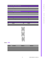
1
User Manual ROM-DB3900 Development Board for RTX v2.0 Modules Copyright The documentation and the software included with this product are copyrighted 2014 by Advantech Co., Ltd. All rights are reserved. Advantech Co., Ltd. reserves the right to make improvements in the products described in this manual at any time without notice. No part of this manual may be reproduced, copied, translated or transmitted in any form or by any means without the prior written permission of Advantech Co., Ltd. Information provided in this manual is intended to be accurate and reliable. However, Advantech Co., Ltd. assumes no responsibility for its use, nor for any infringements of the rights of third parties, which may result from its use. Acknowledgements ARM is trademarks of ARM Corporation. Freescale is trademarks of Freescale Corporation. Microsoft Windows are registered trademarks of Microsoft Corp. All other product names or trademarks are properties of their respective owners. Product Warranty (2 years) Advantech warrants to you, the original purchaser, that each of its products will be free from defects in materials and workmanship for two years from the date of purchase. This warranty does not apply to any products which have been repaired or altered by persons other than repair personnel authorized by Advantech, or which have been subject to misuse, abuse, accident or improper installation. Advantech assumes no liability under the terms of this warranty as a consequence of such events. Because of Advantech’s high quality-control standards and rigorous testing, most of our customers never need to use our repair service. If an Advantech product is defective, it will be repaired or replaced at no charge during the warranty period. For outof-warranty repairs, you will be billed according to the cost of replacement materials, service time and freight. Please consult your dealer for more details. If you think you have a defective product, follow these steps: 1. Collect all the information about the problem encountered. (For example, CPU speed, Advantech products used, other hardware and software used, etc.) Note anything abnormal and list any onscreen messages you get when the problem occurs. 2. Call your dealer and describe the problem. Please have your manual, product, and any helpful information readily available. 3. If your product is diagnosed as defective, obtain an RMA (return merchandize authorization) number from your dealer. This allows us to process your return more quickly. 4. Carefully pack the defective product, a fully-completed Repair and Replacement Order Card and a photocopy proof of purchase date (such as your sales receipt) in a shippable container. A product returned without proof of the purchase date is not eligible for warranty service. 5. Write the RMA number visibly on the outside of the package and ship it prepaid to your dealer. ROM-DB3900 User Manual Part No. 2006B39001 Edition 2 Printed in Taiwan December 2014 ii Declaration of Conformity FCC Class B Note: This equipment has been tested and found to comply with the limits for a Class B digital device, pursuant to part 15 of the FCC Rules. These limits are designed to provide reasonable protection against harmful interference in a residential installation. This equipment generates, uses and can radiate radio frequency energy and, if not installed and used in accordance with the instructions, may cause harmful interference to radio communications. However, there is no guarantee that interference will not occur in a particular installation. If this equipment does cause harmful interference to radio or television reception, which can be determined by turning the equipment off and on, the user is encouraged to try to correct the interference by one or more of the following measures: Reorient or relocate the receiving antenna. Increase the separation between the equipment and receiver. Connect the equipment into an outlet on a circuit different from that to which the receiver is connected. Consult the dealer or an experienced radio/TV technician for help. iii ROM-DB3900 User Manual Warnings, Cautions and Notes Warning! Warnings indicate conditions, which if not observed, can cause personal injury! Caution! Cautions are included to help you avoid damaging hardware or losing data. e.g. There is a danger of a new battery exploding if it is incorrectly installed. Do not attempt to recharge, force open, or heat the battery. Replace the battery only with the same or equivalent type recommended by the manufacturer. Discard used batteries according to the manufacturer's instructions. Note! Notes provide optional additional information. Packing List Before installation, please ensure the following items have been shipped. 9696M39000E RTX 2.0 Carrier board ROM-DB3900 1 9696ED2000E debug adapter board 1 1700021882-01 LVDS backlight cable 1 1700021883-01 LVDS cable 1 1700021941-01 SATA power 1 1700004711 SATA signal 1 1700019076 USB OTG to Type A female 1 1700019077 USB OTG to Type A male 1 1701100300 F Cable IDE#3 10P-2.54/D-SUB 9P(M) 30cm for UART and 2 CAN 1700021861-01 USB 4 pin to Type A Cable 1 1700022373-01 Debug port cable for ROM-3420 1 1700019474 A Cable D-SUB 9P(F)/D-SUB 9P(F) RS232/RS485 100c 1 2026390000 China RoHS ROM-DB3900 Electronic Pollution 1st 1 Optional Accessories Part No. Description 9696MEG510E Daughter board for audio codec 9696MX5300E Daughter board for system bus 9680015491 PCIe to miniPCIe adapter card 96LEDKA070WV40NB1 7" LCD AUO G070VW01 V0 w/o touch ROM-DB3900 User Manual iv RTX 2.0 CPU Boards Part No. Description ROM-3420CD-MDA1E Freescale i.mx6 Dual core 1GHz with 1GB memory (0~60C) ROM-3420WD-MDA1E Freescale i.mx6 Dual core 1GHz with 1GB memory(-40~85C) ROM-3420CQ-MDA1E Freescale i.mx6 Quad core 1GHz with 1GB memory(0~60C) ROM-3420WQ-MDA1E Freescale i.mx6 Quad core 1GHz with 1GB memory(-40~85C) For more information please refer to "Advantech Baseboard Check List" and "Evaluation Board Reference Schematic". You can download "Advantech Baseboard Check List" and "Evaluation Board Reference Schematic" from http://www.advantech.com Safety Instructions 1. 2. 3. 4. 5. 6. 7. 8. 9. 10. 11. 12. 13. 14. 15. Read these safety instructions carefully. Keep this User Manual for later reference. Disconnect this equipment from any AC outlet before cleaning. Use a damp cloth. Do not use liquid or spray detergents for cleaning. For plug-in equipment, the power outlet socket must be located near the equipment and must be easily accessible. Keep this equipment away from humidity. Put this equipment on a reliable surface during installation. Dropping it or letting it fall may cause damage. The openings on the enclosure are for air convection. Protect the equipment from overheating. DO NOT COVER THE OPENINGS. Make sure the voltage of the power source is correct before connecting the equipment to the power outlet. Position the power cord so that people cannot step on it. Do not place anything over the power cord. All cautions and warnings on the equipment should be noted. If the equipment is not used for a long time, disconnect it from the power source to avoid damage by transient overvoltage. Never pour any liquid into an opening. This may cause fire or electrical shock. Never open the equipment. For safety reasons, the equipment should be opened only by qualified service personnel. If one of the following situations arises, get the equipment checked by service personnel: The power cord or plug is damaged. Liquid has penetrated into the equipment. The equipment has been exposed to moisture. The equipment does not work well, or you cannot get it to work according to the user's manual. The equipment has been dropped and damaged. The equipment has obvious signs of breakage. DO NOT LEAVE THIS EQUIPMENT IN AN ENVIRONMENT WHERE THE STORAGE TEMPERATURE MAY GO BELOW -20° C (-4° F) OR ABOVE 60° C (140° F). THIS COULD DAMAGE THE EQUIPMENT. THE EQUIPMENT SHOULD BE IN A CONTROLLED ENVIRONMENT. v ROM-DB3900 User Manual 16. CAUTION: DANGER OF EXPLOSION IF BATTERY IS INCORRECTLY REPLACED. REPLACE ONLY WITH THE SAME OR EQUIVALENT TYPE RECOMMENDED BY THE MANUFACTURER, DISCARD USED BATTERIES ACCORDING TO THE MANUFACTURER'S INSTRUCTIONS. The sound pressure level at the operator's position according to IEC 704-1:1982 is no more than 70 dB (A). DISCLAIMER: This set of instructions is given according to IEC 704-1. Advantech disclaims all responsibility for the accuracy of any statements contained herein. Safety Precaution - Static Electricity Follow these simple precautions to protect yourself from harm and the products from damage. To avoid electrical shock, always disconnect the power from your PC chassis before you work on it. Don't touch any components on the CPU card or other cards while the PC is on. Disconnect power before making any configuration changes. The sudden rush of power as you connect a jumper or install a card may damage sensitive electronic components. ROM-DB3900 User Manual vi Contents Chapter Chapter 1 General Introduction ...........................1 1.1 1.2 Introduction ............................................................................................... 2 Product Specification ................................................................................ 2 2 H/W Installation....................................3 2.1 2.2 2.3 Module Form Factor.................................................................................. 4 Environmental Specifications .................................................................... 4 ROM-DB3900 Appearance ....................................................................... 4 2.3.1 ROM-DB3900 Overview ............................................................... 4 2.3.2 I/O Connectors.............................................................................. 5 Connectors, Jumper settings, Switches and LEDs ................................... 5 2.4.1 Rear I/O panel............................................................................... 5 Table 2.1: External IO Connector ................................................ 5 Table 2.2: DCIN (DC-Jack, +19V power input)............................ 5 Table 2.3: COM01A (UART0, 4 WIRE) ....................................... 6 Table 2.4: COM01B (UART1, 4 WIRE) ....................................... 6 Table 2.5: VGA (VGA) ................................................................. 7 Table 2.6: HDMI (HDMI).............................................................. 7 Table 2.7: RJ45+USB (RJ-45 & USB 1/2) ................................... 8 Table 2.8: PHONE_JACK (Audio output) .................................... 8 2.4.2 Internal I/O .................................................................................... 9 Table 2.9: Internal IO Connectors ............................................... 9 2.4.3 Connectors.................................................................................. 11 Table 2.10: PCIE_SLOT0 (PCIex1 connector1).......................... 11 Table 2.11: PCIE_SLOT1 (PCIex1 connector2).......................... 12 Table 2.12: SATA (SATA connector)........................................... 13 Table 2.13: SATA_PWR (SATA Power connector) ..................... 13 Table 2.14: LVDS (LVDS 24-bit) ................................................. 14 Table 2.15: LVDS_BKLT (LVDS backlight power) ...................... 14 Table 2.16: USB_OTG (USB OTG)............................................. 14 Table 2.17: SD (SD slot).............................................................. 15 Table 2.18: BR2032HOLDER (CR-2032).................................... 15 2.4.4 Jumpers ...................................................................................... 15 Table 2.19: JP2201 (GPIO/Keypad selection for GPIO0/10) ...... 15 Table 2.20: JP2202 (GPIO/Keypad selection for GPIO1/11) ...... 15 Table 2.21: JP2203 (GPIO/Keypad selection for GPIO2/12) ...... 16 Table 2.22: JP2204 (GPIO/Keypad selection for GPIO3/13) ...... 16 Table 2.23: JP2205 (GPIO/Keypad selection for GPIO4/14) ...... 16 Table 2.24: JP2206 (GPIO/Keypad selection for GPIO5/15) ...... 16 Table 2.25: JP2207 (GPIO/Keypad selection for GPIO6/16) ...... 16 Table 2.26: JP2208 (GPIO/Keypad selection for GPIO7/17) ...... 17 Table 2.27: JP2208 (GPIO8) ....................................................... 17 Table 2.28: JP22 (GPIO9) ........................................................... 17 Table 2.29: JP1801~JP1804, JP1901~JP1904 (UART 120om terminal resister) ........................................................... 17 Table 2.30: JP1101 (EDP_HPD for LVDS) ................................. 18 Table 2.31: JP1601 (SATA-DOM Jumper, default 2-3) ............... 18 Table 2.32: JP1701 (CAN0 bus, 120OM terminal resistor) ......... 18 Table 2.33: JP1702 (CAN1 bus, 120OM terminal resistor) ......... 18 Table 2.34: COM_SEL0/1/2/3 (UART0/1/2/3 function selection.. 19 Table 2.35: (UART1, 2wires) ....................................................... 19 Table 2.36: (UART3, 2wires) ....................................................... 20 Table 2.37: CAM0 (Camera 1, MIPI) ........................................... 20 2.4 vii ROM-DB3900 User Manual 2.4.5 2.4.6 2.4.7 2.4.8 Chapter Table 2.38: CAM2 (Camera 2, MIPI)........................................... 21 Table 2.39: GPIO (GPIO) ............................................................ 21 Table 2.40: JP2301 (External WDT) ........................................... 22 Table 2.41: FAN (System FAN)................................................... 22 Table 2.42: AUDIO (I2S0, audio codec)...................................... 22 Table 2.43: SPI1 (SPI1) .............................................................. 23 Table 2.44: SPI0 (SPI0) .............................................................. 23 Table 2.45: LVDS_BK_SLT (LVDS backlight selection) ............. 23 Table 2.46: LVDS_VDD_SLT1 (LVDS VDD Power selection) .... 23 Table 2.47: LVDS_VDD_SLT2 (LVDS VDD Power selection2) .. 24 Table 2.48: CAN0 (CAN bus 0) ................................................... 24 Table 2.49: CAN0 (CAN bus 0) ................................................... 24 Table 2.50: RTXA Connector ...................................................... 25 Table 2.51: RTXB Connector ...................................................... 26 Table 2.52: RTXC Connector ...................................................... 27 Table 2.53: RTXD Connector ...................................................... 28 Table 2.54: SYSTEM BUS .......................................................... 29 Switches and buttons.................................................................. 30 Table 2.55: SW2 (Boot selection)................................................ 30 Table 2.56: SW3 (Reset button).................................................. 31 Table 2.57: SW5 (Sleep button) .................................................. 31 Table 2.58: SW4 (Power button, CPU) ....................................... 31 Table 2.59: SW6 (LID Switch) ..................................................... 31 LEDs ........................................................................................... 31 PCB Footprint of Board to Board Connector .............................. 32 Module Board Installation ........................................................... 32 3 Advantech Services.......................... 33 3.1 3.2 3.3 3.4 RISC Design-in Services ........................................................................ 34 Contact Information................................................................................. 37 Technical Support and Assistance.......................................................... 38 Global Service Policy .............................................................................. 38 3.4.1 Warranty Policy........................................................................... 38 3.4.2 Warranty Period.......................................................................... 38 3.4.3 Repairs under Warranty.............................................................. 38 3.4.4 Exclusions from Warranty........................................................... 39 Repair Process ....................................................................................... 39 3.5.1 Obtaining an RMA Number......................................................... 39 3.5.2 Returning the Product for Repair ................................................ 39 3.5.3 Service Charges ......................................................................... 40 3.5.4 Repair Report ............................................................................. 41 3.5.5 Custody of Products Submitted for Repair ................................. 41 3.5.6 Shipping Back to Customer ........................................................ 41 3.5 ROM-DB3900 User Manual viii Chapter 1 1 General Introduction This chapter gives background information on the ROM-DB3900. Sections include: Introduction Specification 1.1 Introduction ROM-DB3900 is an evaluation carrier board designed for the Advantech RTX module. It is compatible with RTX module ROM-3420 and has rich I/O interface for evaluation and development. It supports wide range operating temperatures, and also supports two MIPI connectors for the camera module. ROM-DB3900 is an ideal development board for ruggedized applications, such as medical device, Industrial control, Transportation/fleet management systems. ROM-DB3900 comes with RISC RTX carrier board design documents: Carrier Board Design Guide, Layout, Schematic checklist, and also the reference board schematics ready for you to start your own carrier board design. +19V DC in power input 2 camera input support 10 GPIO 4 UART and 2 CAN ports 1.2 Product Specification Compatible Module Graphic Ethernet Storage I/O Expansion Power input Environment Advantech RTX 2.0 CPU Module Series HDMI 1 HDMI TypeA LVDS 1 single channel 24-bit LVDS VGA 1 D-Sub 15 with female connector 10/100/100 Mbps 1 RJ45 eMMC Onboard 4GB eMMC EEPROM Onboard 4KB EEPROM SD 1 SD card slot SATA 1 SATAII Connector (with SATA-DOM support) USB 1 USB Mini Type B (OTG), 1 USD 2.0/3.0 Type A UART 4 UART Ports (4 wires) Audio 1 2 port phone jack, support line-in, line-out CAN 2 CAN 2.0B ports, Differential mode +5V GPIO 10 GPIO Ports I2C 2 I2C pin header SPI 2 SPI pin header Camera input 2 MIPI connectors System Bus 1 PC104 Connector (Address:31 bits, Data: 16 bits) KeyPad 4x4 Keypad (share pin with GPIO, By software setting) I2S 1 Pin header PCIe slot 2 PCIe x1 Power + 19V DC Jack Operation 0~60°C (32~140°F) Operating Humidity 0% ~ 90% relative humidity, non-condensing Physical Dimensions Characteristics ROM-DB3900 User Manual 305 x 244 mm (12" x 9.6") 2 Chapter 2 2 H/W Installation This chapter gives mechanical and connector information on the ROM-DB3900 carrier board. Sections include: Connector Information Mechanical Drawing Hardware Installation 2.1 Module Form Factor RTX form factor size, 68mm (W) x 68mm (D) 2.2 Environmental Specifications Operating temperature: 0~60 °C (32~140°F) The operating temperature refers to the environmental temperature for the model. Operating humidity: 0% ~ 90% relative humidity, non-condensing Storage temperature: -40~85 °C Relative humidity: 95% @ 60 °C Weight (g): 80 g (weight of total package) 2.3 ROM-DB3900 Appearance 2.3.1 ROM-DB3900 Overview ROM-DB3900 User Manual 4 Chapter 2 2.3.2 I/O Connectors 2.4.1 Rear I/O panel Table 2.1: External IO Connector Position Description DCIN DC Jack A COM01A UART Port 1 B COM01B UART Port 2 C HDMI HDMI Port D VGA VGA Port E RJ45+USB GbE Ethernet Connector F RJ45+USB USB Port 1/ 2 G PHONE_JACK MIC Input/ Audio Output H Table 2.2: DCIN (DC-Jack, +19V power input) Pin Signal Pin Signal 1 +19V Shield GND 5 ROM-DB3900 User Manual H/W Installation 2.4 Connectors, Jumper settings, Switches and LEDs Table 2.3: COM01A (UART0, 4 WIRE) Pin Signal Pin Signal 1 TXD485- 2 RXD/TXD485+ 3 TXD/RXD485+TX 4 RXD485- 5 GND 6 - 7 RTS 8 CTS 9 - Table 2.4: COM01B (UART1, 4 WIRE) Pin Signal Pin Signal 1 TXD485- 2 RXD/TXD485+ 3 TXD/RXD485+ 4 RXD485- 5 GND 6 - 7 RTS 8 CTS 9 - ROM-DB3900 User Manual 6 Chapter 2 Table 2.5: VGA (VGA) Pin Signal Pin Signal 1 Red 2 Green 3 Blue 4 - 5 GND 6 GND 7 GND 8 GND +5V 10 GND 11 - 12 DDC_DAT 13 HSYNC 14 VSYNC 15 DDC_CK Pin Signal Table 2.6: HDMI (HDMI) Pin Signal 1 TMDS_D2+ 2 GND 3 TMDS_D2- 4 TMDS_D1+ 5 GND 6 TMDS_D1- 7 TMDS_D0+ 8 GND 9 TMDS_D0- 10 TMDS_CLK+ 11 GND 12 TMDS_CLK- 13 CEC 14 - 15 CTRL_CLK 16 CTRL_DAT 17 GND 18 +5V 19 HPD 7 ROM-DB3900 User Manual H/W Installation 9 Table 2.7: RJ45+USB (RJ-45 & USB 1/2) 1 DA+ Pin Signal 2 DA- U1 VBUS 3 DB+ U2 D- 4 DC+ U3 D+ 5 DC- U4 GND 6 DB- U5 SS_RX- 7 DD+ U6 SS_RX+ 8 DD- U7 GND L3 GBE_LINK1000# U8 SS_TX- U9 SS_TX+ Table 2.8: PHONE_JACK (Audio output) Pin Signal Pin Signal 1 GND 22 Audio_L 2 - 23 GND 3 GND 24 GND 4 GND 25 Audio_R 5 MIC_IN Line out: stereo, Line in: mono ROM-DB3900 User Manual 8 Chapter 2 2.4.2 Internal I/O H/W Installation Table 2.9: Internal IO Connectors Position Description Connector type DCIN DC-in DC POWER JACK 2.5mm 90D(M) DIP 2DCG213B200 COM01 COM Port D-SUB Conn. 18P 90D(M) DIP DM10151-H531-4F HDMI HDMI HDMI Conn. 19P 0.5mm 90D(F) SMD QJ51191LFB4-7F VGA VGA D-SUB Conn. 15P 90D(F) DIP 070242FR015S200ZU RJ45+USB LAN+USB PhoneJack RJ45+USB3.0*2 32P 90D(F) DIP 05A00919 Phone Jack PhoneJack Audio Jack 9P 2.5mm 90D(F) DIP ABA-JAK-03 Audio Audio PIN HEADER 2x10P 2.54mm 180D(M) DIP 21N22564 LVDS LVDS B/B Conn. 40P 1.25mm 90D SMD DF13-40DP1.25V(91) FAN FAN Wafer 2.54mm 3P 180D(M) DIP 22-27-2031 SATA_PWR SATA power WAFER 4P 2.5mm 180D(M) DIP 24W1161-04S1001T PCIE_SLOT0 PCIE_SLOT0 PCIEXPRESS 36P 180D(F) DIP 2EG01817-D2D-DF PCIE_SLOT1 PCIE_SLOT1 PCIEXPRESS 36P 180D(F) DIP 2EG01817-D2D-DF SATA SATA Serial ATA 7P 1.27mm 180D(M) DIP WATM07DBN4A3B8 GPIO GPIO PIN HEADER 10x2P 2.0mm 180D(M) DIP 21N22050 LVDS_BKLT LVDS Backlight WAFER BOX 2.0mm 5P 180D(M) DIP WO/Pb JIH VEI SW3 Reset button TACT SW STS-091 SMD 4P H=3.8mm 9 ROM-DB3900 User Manual Table 2.9: Internal IO Connectors SW4 Power button TACT SW STS-091 SMD 4P H=3.8mm SW5 Sleep button TACT SW STS-091 SMD 4P H=3.8mm SW6 Wake up button TACT SW STS-091 SMD 4P H=3.8mm SPI0 SPI0 PIN HEADER 2x4P 2.54mm 180D(M) DIP 210-9204GB02 SPI1 SPI1 PIN HEADER 2x4P 2.54mm 180D(M) DIP 210-9204GB02 SW2 Boot selection DIP SW EDG104S DIP 4P Radial SPST COM3 COM3 BOX HEADER 5x2P 2.54mm 180D(M) DIP 23N696010S10 COM2 COM2 BOX HEADER 5x2P 2.54mm 180D(M) DIP 23N696010S10 CAN1 CAN1 BOX HEADER 5x2P 2.54mm 180D(M) DIP 23N696010S10 CAN0 CAN0 BOX HEADER 5x2P 2.54mm 180D(M) DIP 23N696010S10 USB_OTG USB OTG MINI USB 5P 180D(F) SMD UH51543-CS7-7F SD SD SD CARD 9P 90D(F) SMD WK2192C-S3D-7H System_Bus SYSTEMBUS PCB SKT 30x4P 2.00mm 180D(F) DIP 264-40303-02 I2C0 I2C0 WAFER BOX 2.0mm 4P 180D(M) W/LOCK A2001WV2-4P I2C1 I2C1 WAFER BOX 2.0mm 4P 180D(M) W/LOCK A2001WV2-4P RTXA,RTXB, RTXC,RTXD RTX B2B Connector B/B Conn. 50x2P 0.5mm 180D(M) SMD AXK500137YG ROM-DB3900 User Manual 10 Chapter 2 2.4.3 Connectors Table 2.10: PCIE_SLOT0 (PCIex1 connector1) Pin Signal Pin Signal B1 +12V A1 +12V B2 +12V A2 +12V B3 +12V A3 +12V B4 GND A4 GND PCIE_A_CK A5 PCIE_A_JTAG2 B6 PCIE_A_DAT A6 PCIE_A_JTAG3 B7 GND A7 PCIE_A_JTAG4 B8 +3V A8 PCIE_A_JTAG5 B9 PCIE_A_JTAG1 A9 +3V B10 +3V A10 +3V B11 +3V A11 PWRGD Mechanical Key B12 Reserved A12 GND B13 GND A13 PCIE_A_REFCK+ B14 PCIE_A_TX+ A14 PCIE_A_REFCK- B15 PCIE_A_TX- A15 GND B16 GND A16 PCIE_A_RX+ B17 +3V A17 PCIE_A_RX- B18 GND A18 GND 11 ROM-DB3900 User Manual H/W Installation B5 Table 2.11: PCIE_SLOT1 (PCIex1 connector2) Pin Signal Pin Signal B1 +12V A1 +12V B2 +12V A2 +12V B3 +12V A3 +12V B4 GND A4 GND B5 PCIE_B_CK A5 PCIE_B_JTAG2 B6 PCIE_B_DAT A6 PCIE_B_JTAG3 B7 GND A7 PCIE_B_JTAG4 B8 +3V A8 PCIE_B_JTAG5 B9 PCIE_B_JTAG1 A9 +3V B10 +3V A10 +3V B11 +3V A11 PWRGD Mechanical Key B12 Reserved A12 GND B13 GND A13 PCIE_B_REFCK+ B14 PCIE_B_TX+ A14 PCIE_B_REFCK- B15 PCIE_B_TX- A15 GND B16 GND A16 PCIE_B_RX+ B17 +3V A17 PCIE_B_RX- B18 GND A18 GND ROM-DB3900 User Manual 12 Pin Signal Pin Signal 1 GND 2 SATA_TX+ 3 SATA_TX- 4 GND 5 SATA_RX- 6 SATA_RX+ 7 SATA DOM PIN7 H/W Installation Table 2.13: SATA_PWR (SATA Power connector) 1 +5V 2 GND 3 GND 4 +12V 13 Chapter 2 Table 2.12: SATA (SATA connector) ROM-DB3900 User Manual Table 2.14: LVDS (LVDS 24-bit) Pin Signal Pin Signal 1 +VDD_LVDS 2 +VDD_LVDS 3 GND 4 GND 5 +VDD_LVDS 6 +VDD_LVDS 7 LVDS_D0- 8 - 9 LVDS_D0+ 10 - 11 GND 12 GND 13 LVDS_D1- 14 - 15 LVDS_D1+ 16 - 17 GND 18 GND 19 LVDS_D2- 20 - 21 LVDS_D2+ 22 - 23 GND 24 GND 25 LVDS_CLK- 26 - 27 LVDS_CLK+ 28 - 29 GND 30 GND 31 DID_CK 32 DID_DAT 33 GND 34 EDP_HDP 35 LVDS D3- 36 - 37 LVDS D3+ 38 - 39 GND 40 LVDS_CTRL Table 2.15: LVDS_BKLT (LVDS backlight power) Pin Signal Pin Signal 1 +VDD_BKLT_LVDS 2 GND 3 BLK_EN 4 Brightness 5 +5V Table 2.16: USB_OTG (USB OTG) Pin Signal Pin Signal 1 VBUS 2 USB_OTG D- 3 USB_OTG D+ 4 OTG ID 5 GND ROM-DB3900 User Manual 14 Chapter 2 Table 2.17: SD (SD slot) Signal Pin Signal 1 SDIO_DATA3_X 2 SDIO_CMD 3 GND 4 +3V 5 SDIO_CK 6 GND 7 SDIO_DATA0 8 SDIO_DATA1 9 SDIO_DATA2 10 SDIO_CD# 11 GND 12 +3V_SDIO H1 - H2 - H3 - H4 GND H5 GND H6 GND Table 2.18: BR2032HOLDER (CR-2032) Pin Signal Pin Signal 1 BAT_RTC 2 GND 2.4.4 Jumpers Table 2.19: JP2201 (GPIO/Keypad selection for GPIO0/10) Pin Signal 1-2 GPIO0 2-3 GPIO10 Table 2.20: JP2202 (GPIO/Keypad selection for GPIO1/11) Pin Signal 1-2 GPIO1 2-3 GPIO11 15 ROM-DB3900 User Manual H/W Installation Pin Table 2.21: JP2203 (GPIO/Keypad selection for GPIO2/12) Pin Signal 1-2 GPIO2 2-3 GPIO12 Table 2.22: JP2204 (GPIO/Keypad selection for GPIO3/13) Pin Signal 1-2 GPIO3 2-3 GPIO13 Table 2.23: JP2205 (GPIO/Keypad selection for GPIO4/14) Pin Signal 1-2 GPIO4 2-3 GPIO14 Table 2.24: JP2206 (GPIO/Keypad selection for GPIO5/15) Pin Signal 1-2 GPIO5 2-3 GPIO15 Table 2.25: JP2207 (GPIO/Keypad selection for GPIO6/16) Pin Signal 1-2 GPIO6 2-3 GPIO16 ROM-DB3900 User Manual 16 Signal 1-2 GPIO7 2-3 GPIO17 H/W Installation Pin Table 2.27: JP2208 (GPIO8) Pin Signal 1-2 GPIO8 2-3 - Table 2.28: JP22 (GPIO9) Pin Signal 1-2 GPIO9 2-3 - Table 2.29: JP1801~JP1804, JP1901~JP1904 (UART 120om terminal resister) Pin Signal 1-2 120 OM (Default) 2-3 Without 120 OM Chapter 2 Table 2.26: JP2208 (GPIO/Keypad selection for GPIO7/17) 17 ROM-DB3900 User Manual Table 2.30: JP1101 (EDP_HPD for LVDS) Pin Signal Pin Signal 1 GND 2 EDP_HDP_A 3 EDP_HPD Table 2.31: JP1601 (SATA-DOM Jumper, default 2-3) Pin Signal Pin Signal 1 +5V 2 SATA-DOM Pin7 3 GND - - Table 2.32: JP1701 (CAN0 bus, 120OM terminal resistor) Jumper Mode Jumper Mode 1-2 120 OM (Default) - Without 120 OM Table 2.33: JP1702 (CAN1 bus, 120OM terminal resistor) Jumper Mode Jumper Mode 1-2 120 OM (Default) - Without 120 OM Jumper Mode Jumper Mode 1-2 120 OM (Default) - Without 120 OM ROM-DB3900 User Manual 18 Signal Pin Signal 1 SER2_RX 2 RXD485_A 3 SER2_RX 4 RXD422_A 5 SER2_RX 6 RXD232_A 7 - 8 COM2_RXD 9 NDCD#TXD485- 10 NRXD2TXD485+ 11 TXD485-_A 12 TXD485+_A 13 COM2_TXD 14 - 15 NTXD2_RXD485+ 16 NDTR#2_RXD485- 17 RSD485+_A 18 RSD485-_A Table 2.35: (UART1, 2wires) Pin Signal Pin Signal 1 TXD485- 2 - 3 COM1_RX 4 RTS 5 COM1_TX 6 CTS 7 RXD485- 8 - 9 GND 10 - 19 ROM-DB3900 User Manual H/W Installation Pin Chapter 2 Table 2.34: COM_SEL0/1/2/3 (UART0/1/2/3 function selection Table 2.36: (UART3, 2wires) Pin Signal Pin Signal 1 TXD485- 2 - 3 RXD/TXD485+ 4 RTS 5 TXD/RXD485+ 6 CTS 7 RXD485- 8 - 9 GND 10 - Table 2.37: CAM0 (Camera 1, MIPI) Pin Signal Pin Signal 1 PCAM_HSYNC 2 PCAM_ON_CSI1 3 PCAM_VSYNC 4 PCAM_PXL_CK1 5 CAM0_PWR 6 GND 7 CAM0_RST 8 I2C_CSI0_DAT 9 GND 10 I2C_CSI0_CK 11 NC 12 GND 13 NC 14 CSI0_X_CK+ 15 GND 16 CSI0_X_CK- 17 NC 18 GND 19 PCAM_MCK 20 CSI0_X_D1+ 21 GND 22 CSI0_X_D1- 23 CSI0_MCK 24 GND 25 +3V 26 CSI0_D0+ 27 +3V 28 CSI0_X_D0- 29 +3V 30 GND ROM-DB3900 User Manual 20 Signal Pin Signal 1 PCAM_FLD 2 PCAM_ON_CSI1 3 PCAM_DE 4 PCAM_PXL_CK0 5 CAM1_PWR 6 GND 7 GND 8 I2C_CSI1_DAT 9 GND 10 I2C_CSI1_CK 11 CSI1_X_D3+ 12 GND 13 CIS1_X_D3- 14 CSI1_X_CK+ 15 GND 16 CSI1_X_CK- 17 CSI1_X_D2+ 18 GND 19 CSI1_X_D2- 20 CSI1_X_D1+ 21 GND 22 CSI1_X_D1- 23 CAM1_X_MCK 24 GND 25 +3V 26 CSI1_X_D0+ 27 +3V 28 CSI1_X_D0- 29 +3V 30 GND Table 2.39: GPIO (GPIO) Pin Signal Pin Signal 1 3.3V 11 GPIO8 2 GND 12 GPIO9 3 GPIO0 KEY_SEL_ROW0 13 GPIO10 KEY_SEL_ROW0 4 GPIO1 KEY_SEL_ROW1 14 GPIO11 KEY_SEL_ROW1 5 GPIO2 KEY_SEL_ROW2 15 GPIO12 KEY_SEL_ROW2 6 GPIO3 KEY_SEL_ROW3 16 GPIO13 KEY_SEL_ROW3 7 GPIO4 KEY_SEL_COL0 17 GPIO14 KEY_SEL_COL0 8 GPIO5 KEY_SEL_COL1 18 GPIO15 KEY_SEL_COL1 9 GPIO6 KEY_SEL_COL2 19 GPIO16 KEY_SEL_COL2 10 GPIO7 KEY_SEL_COL3 20 GPIO17 KEY_SEL_COL3 21 ROM-DB3900 User Manual H/W Installation Pin Chapter 2 Table 2.38: CAM2 (Camera 2, MIPI) Table 2.40: JP2301 (External WDT) Pin Signal Pin Signal 1 WDT_Time_Out# 2 GND Table 2.41: FAN (System FAN) Pin Signal Pin Signal 1 GND 2 +12V 3 +5V Table 2.42: AUDIO (I2S0, audio codec) Pin Signal Pin Signal 1 Audio_VDDA 2 GND 3 Audio_VDDA 4 I2S0_SDIN_C 5 I2S0_SDOUT_C 6 I2S0_LRCK_C 7 I2S0_CK_C 8 AUDIO_MCK_C 9 - 10 GND 11 Audio_I2C_CK 12 MIC_BIAS 13 Audio_I2C_DAT 14 GND 15 - 16 HP_R 17 MIC_IN 18 GND 19 GND 20 HP_L ROM-DB3900 User Manual 22 Pin Signal Pin Signal 1 +3V 2 GND 3 SPI1_CS0# 3 SPI1_CK 5 SPI1_DO_C 6 SPI1_DIN_C 7 - 8 SPI1_CS1#_C Pin Signal Pin Signal 1 +3V 2 GND 3 SPI0_CS0# 3 SPI0_CK 5 SPI0_DO_C 6 SPI0_DIN_C 7 - 8 SPI0_CS1#_C Table 2.45: LVDS_BK_SLT (LVDS backlight selection) Jumper Mode Jumper Mode 1-2 +5V (Default) 2-3 +12V * +VDD_BKLT_LVDS, pin1 Table 2.46: LVDS_VDD_SLT1 (LVDS VDD Power selection) Jumper Mode Jumper Mode 1-2 +3.3V 2-3 +5V 23 ROM-DB3900 User Manual H/W Installation Table 2.44: SPI0 (SPI0) Chapter 2 Table 2.43: SPI1 (SPI1) Table 2.47: LVDS_VDD_SLT2 (LVDS VDD Power selection2) Jumper Mode 1-2 +12V Jumper Mode Table 2.48: CAN0 (CAN bus 0) Pin Signal Pin Signal 1 - 2 - 3 CAN0_D- 4 - 5 CAN0_D+ 6 - 7 - 8 - 9 GND 10 - Table 2.49: CAN0 (CAN bus 0) Pin Signal Pin Signal 1 - 2 - 3 CAN0_D- 4 - 5 CAN0_D+ 6 - 7 - 8 - 9 GND 10 - ROM-DB3900 User Manual 24 Odd Number RTX V2.0a I/F Even Number RTX V2.0a I/F GND PWR A2 GND PWR A3 SYSBUS_D0 I/O A4 SYSBUS_D8 I/O A5 SYSBUS_D1 I/O A6 SYSBUS_D9 I/O A7 SYSBUS_D2 I/O A8 SYSBUS_D10 I/O A9 SYSBUS_D3 I/O A10 SYSBUS_D11 I/O A11 SYSBUS_D4 I/O A12 SYSBUS_D12 I/O A13 SYSBUS_D5 I/O A14 SYSBUS_D13 I/O A15 SYSBUS_D6 I/O A16 SYSBUS_D14 I/O A17 SYSBUS_D7 I/O A18 SYSBUS_D15 I/O A19 GND PWR A20 GND PWR A21 SYSBUS_A0 O A22 SYSBUS_A8 O A23 SYSBUS_A1 O A24 SYSBUS_A9 O A25 SYSBUS_A2 O A26 SYSBUS_A10 O A27 SYSBUS_A3 O A28 SYSBUS_A11 O A29 SYSBUS_A4 O A30 SYSBUS_A12 O A31 SYSBUS_A5 O A32 SYSBUS_A13 O A33 SYSBUS_A6 O A34 SYSBUS_A14 O A35 SYSBUS_A7 O A36 SYSBUS_A15 O A37 GND PWR A38 GND PWR A39 SYSBUS_A16 O A40 SYSBUS_A24 O A41 SYSBUS_A17 O A42 SYSBUS_A25 O A43 SYSBUS_A18 O A44 SYSBUS_A26 O A45 SYSBUS_A19 O A46 SYSBUS_A27 O A47 SYSBUS_A20 O A48 SYSBUS_A28 O A49 SYSBUS_A21 O A50 SYSBUS_A29 O A51 SYSBUS_A22 O A52 SYSBUS_A30 O A53 SYSBUS_A23 O A54 ? ? A55 GND PWR A56 GND PWR A57 SYSBUS_INT0 I A58 SYSBUS_INT2 I A59 SYSBUS_INT1 I A60 SYSBUS_INT3 I A61 GND PWR A62 GND PWR A63 SYSBUS_ALE O A64 SYSBUS_WAIT# I A65 SYSBUS_BE0# O A66 SYSBUS_CS0# O A67 SYSBUS_BE1# O A68 SYSBUS_CS1# O A69 SYSBUS_WE# O A70 GND PWR A71 SYSBUS_OE# O A72 SYSBUS_CLK O A73 RESET_IN# I/PU A74 GND PWR A75 RESET_OUT# OD A76 WAKE# I/PU A77 CB_PWR_EN O A78 SLEEP# I/PU A79 CB_PGOOD I/PU A80 SUSPEND_REQ# O A81 RTX_PGOOD I/PU A82 WDT_OUT# O A83 RTC_PWR PWR A84 POWER_BTN# I/PU A85 GND PWR A86 GND PWR A87 VCC PWR A88 VCC PWR 25 ROM-DB3900 User Manual H/W Installation A1 Chapter 2 Table 2.50: RTXA Connector Table 2.50: RTXA Connector A89 VCC PWR A90 VCC PWR A91 VCC PWR A92 VCC PWR A93 VCC PWR A94 VCC PWR A95 VCC PWR A96 VCC PWR A97 VCC PWR A98 VCC PWR A99 GND PWR A100 GND PWR Table 2.51: RTXB Connector Odd Number RTX V2.0a I/F Even Number RTX V2.0a I/F B1 GND PWR B2 GND PWR B3 BOOT_SEL0# I/PU B4 TTL_R0 O B5 BOOT_SEL1# I/PU B6 TTL_R1 O B7 BOOT_SEL2# I/PU B8 TTL_R2 O B9 GND PWR B10 TTL_R3 O B11 TTL_HSYNC O B12 TTL_R4 O B13 TTL_VSYNC O B14 TTL_R5 O B15 TTL_DE O B16 TTL_R6 O B17 GND PWR B18 TTL_R7 O B19 TTL_PCLK O B20 GND PWR B21 GND PWR B22 TTL_G0 O B23 I2C3_DATA(for TTL) I/O B24 TTL_G1 O B25 I2C3_CLK(for TTL) O B26 TTL_G2 O B27 GND PWR B28 TTL_G3 O B29 VDD_SD0_EN O B30 TTL_G4 O B31 SD0_CD# I/PU B32 TTL_G5 O B33 SD0_WP I/PU B34 TTL_G6 O B35 GND PWR B36 TTL_G7 O B37 SD0_CMD I/O B38 GND PWR B39 SD0_D0 I/O B40 TTL_B0 O B41 SD0_D1 I/O B42 TTL_B1 O B43 SD0_D2 I/O B44 TTL_B2 O B45 SD0_D3 I/O B46 TTL_B3 O B47 SD0_CLK O B48 TTL_B4 O B49 GND PWR B50 TTL_B5 O B51 VDD_SD1_EN O B52 TTL_B6 O B53 SD1_CD# I/PU B54 TTL_B7 O B55 SD1_WP I/PU B56 GND PWR B57 GND PWR B58 SD1_CMD I/O B59 SPI0_MISO I B60 SD1_D0 I/O B61 SPI0_MOSI O B62 SD1_D1 I/O B63 SPI0_CS0# O B64 SD1_D2 I/O B65 SPI0_CS1# O B66 SD1_D3 I/O B67 SPI0_CLK O B68 SD1_D4 I/O B69 GND PWR B70 SD1_D5 I/O B71 SPI1_MISO I B72 SD1_D6 I/O ROM-DB3900 User Manual 26 SPI1_MOSI O B74 SD1_D7 I/O B75 SPI1_CS0# O B76 SD1_CLK O B77 SPI1_CS1# O B78 GND PWR B79 SPI1_CLK O B80 GPIO0 I/O B81 GND PWR B82 GPIO1 I/O B83 GPIO10/ROW0 I/O B84 GPIO2 I/O B85 GPIO11/ROW1 I/O B86 GPIO3 I/O B87 GPIO12/ROW2 I/O B88 GPIO4 I/O B89 GPIO13/ROW3 I/O B90 GPIO5 I/O B91 GPIO14/COL0 I/O B92 GPIO6 / BAT IN I/O B93 GPIO15/COL1 I/O B94 GPIO7 / BAT THRM I/O B95 GPIO16/COL2 I/O B96 GPIO8 / Timer IN I/O B97 GPIO17/COL3 I/O B98 GPIO9 / Timer Out I/O B99 GND PWR B100 GND PWR Table 2.52: RTXC Connector Odd Number RTX V2.0a I/F Even Number RTX V2.0a I/F C1 GND PWR C2 GND PWR C3 CSI1_D3- / PCAM_D9 DP/I C4 CSI0_D1- / PCAM_D15 DP/I C5 CSI1_D3+ / PCAM_D8 DP/I C6 CSI0_D1+ / PCAM_D14 DP/I C7 GND PWR C8 GND PWR C9 CSI1_D2- / PCAM_D7 DP/I C10 CSI0_D0- / PCAM_D13 DP/I C11 CSI1_D2+ / PCAM_D6 DP/I C12 CSI0_D0+ / PCAM_D12 DP/I C13 GND PWR C14 GND PWR C15 CSI1_D1- / PCAM_D5 DP/I C16 CSI0_CK- / PCAM_D11 DP/I C17 CSI1_D1+ / PCAM_D4 DP/I C18 CSI0_CK+ / PCAM_D10 DP/I C19 GND PWR C20 GND PWR C21 CSI1_D0- / PCAM_D3 DP/I C22 PCAM_MCK O C23 CSI1_D0+ / PCAM_D2 DP/I C24 GND PWR C25 GND PWR C26 PCAM_HSYNC I C27 CSI1_CK- / PCAM_D1 DP/I C28 PCAM_VSYNC I C29 CSI1_CK+ / PCAM_D0 DP/I C30 PCAM_DE I C31 GND PWR C32 PCAM_FLD I C33 CAM_MCK O C34 PCAM_PXL_CK1 I C35 GND PWR C36 GND PWR C37 PCAM_PXL_CK0 I C38 PCIE1_TX+ DP C39 GND PWR C40 PCIE1_TX- DP C41 PCIE0_TX+ DP C42 GND PWR C43 PCIE0_TX- DP C44 PCIE1_RX+ DP C45 GND PWR C46 PCIE1_RX- DP C47 PCIE0_RX+ DP C48 GND PWR C49 PCIE0_RX- DP C50 PCIE1_CLK+ DP C51 GND PWR C52 PCIE1_CLK- DP C53 PCIE0_CLK+ DP C54 GND PWR C55 PCIE0_CLK- DP C56 PCIE1_PWR_EN O 27 ROM-DB3900 User Manual H/W Installation B73 Chapter 2 Table 2.51: RTXB Connector Table 2.52: RTXC Connector C57 GND PWR C58 PCIE1_RST# O C59 PCIE0_PWR_EN O C60 PCIE_WAKE# I/PU C61 PCIE0_RST# O C62 GND PWR C63 GND PWR C64 GBE_XFMR_VREF PWR C65 GBE_MDI0+ DP C66 GBE_LINK_ACT# OD C67 GBE_MDI0- DP C68 GBE_LINK100# OD C69 GND PWR C70 GBE_LINK1000# OD C71 GBE_MDI1+ DP C72 GND PWR C73 GBE_MDI1- DP C74 USB_OTG_PWR_EN O C75 GND PWR C76 USB_OTG_OC# I C77 GBE_MDI2+ DP C78 USB_OTG_ID I C79 GBE_MDI2- DP C80 USB_OTG_VBUS_DET I C81 GND PWR C82 GND PWR C83 GBE_MDI3+ DP C84 USB_OTG_D+ DP C85 GBE_MDI3- DP C86 USB_OTG_D- DP C87 GND PWR C88 GND PWR C89 USB_HOST_PWR_EN O C90 USB_HOST_D+ DP C91 USB_HOST_OC# I C92 USB_HOST_D- DP C93 GND PWR C94 GND PWR C95 USB_SS_TX+ DP C96 USB_SS_RX+ DP C97 USB_SS_TX- DP C98 USB_SS_RX- DP C99 GND PWR C100 GND PWR Table 2.53: RTXD Connector Odd RTX V2.0a Number I/F Even RTX V2.0a Number I/F D1 GND PWR D2 GND PWR D3 SATA_TX+ DP D4 D5 SATA_TX- DP D6 D7 GND PWR D8 D9 SATA_RX+ DP D10 PWR D11 SATA_RX- DP D12 D13 GND PWR D14 D15 SATA_PWR_EN O D16 D17 TTL_VDD_EN O D18 D19 LCD_VDD_EN / eDP VDD_EN O D20 GND D21 eDP_HPD I D22 I2C0_DATA (for Battery / I/O RTC) D23 LCD_BKLT_EN / eDP BKLT_EN O D24 I2C0_CLK (for Battery / RTC) O D25 LCD_BKLT_PWM / eDP BKLT_PWM O D26 I2C1_DATA (CODEC) I/O D27 GND PWR D28 I2C1_CLK (CODEC) O D29 LVDS_D0- / EDP_TX0- DP D30 I2C2_DATA(For Camera/ I/O LVDS) D31 LVDS_D0+ / EDP_TX0+ DP D32 I2C2_CLK(For Camera/ LVDS) ROM-DB3900 User Manual 28 O GND PWR D34 GND PWR D35 LVDS_D1- / EDP_TX1- DP D36 CAN0_TX O D37 LVDS_D1+ / EDP_TX1+ DP D38 CAN0_RX I D39 GND PWR D40 CAN1_TX O D41 LVDS_D2- / EDP_TX2- DP D42 CAN1_RX I D43 LVDS_D2+ / EDP_TX2+ DP D44 GND PWR D45 GND PWR D46 I2S_BCLK O D47 LVDS_CLK- / EDP_AUX- DP D48 I2S_DIN I D49 LVDS_CLK+ / EDP_AUX+ DP D50 I2S_DOUT O D51 GND PWR D52 I2S_LRCLK O D53 LVDS_D3- / EDP_TX3- DP D54 I2S_MCLK O D55 LVDS_D3+ / EDP_TX3+ DP D56 GND PWR D57 GND PWR D58 UART0_TX O D59 HDMI_D2+ DP D60 UART0_RX I D61 HDMI_D2- DP D62 UART0_RTS# O D63 GND PWR D64 UART0_CTS# I D65 HDMI_D1+ DP D66 UART1_TX O D67 HDMI_D1- DP D68 UART1_RX I D69 GND PWR D70 UART1_RTS# O D71 HDMI_D0+ DP D72 UART1_CTS# I D73 HDMI_D0- DP D74 GND PWR D75 GND PWR D76 UART2_TX O D77 HDMI_CK+ DP D78 UART2_RX I D79 HDMI_CK- DP D80 UART2_RTS# O D81 GND PWR D82 UART2_CTS# I D83 HDMI_CEC I/O D84 UART3_TX O D85 HDMI_HPD I D86 UART3_RX I D87 HDMI_DDC_SDA I/O D88 UART3_RTS# O D89 HDMI_DDC_SCL O D90 UART3_CTS# I D91 GND PWR D92 GND PWR D93 PCAM_ON_CSI1# O D94 PCAM_ON_CSI0# O D95 CAM1_PWR# O D96 CAM0_PWR# O D97 CAM1_RST# O D98 CAM0_RST# O D99 GND PWR D100 GND PWR Table 2.54: SYSTEM BUS A B C D 1 N/C GND N/C N/C 2 GND N/C 3.3V 3.3V 3 SYSBUS_INT3 SYSBUS_INT2 SYSBUS_INT1 SYSBUS_INT0 4 N/C SYSBUS_A30 3.3V 3.3V 5 SYSBUS_A0 SYSBUS_A1 SYSBUS_A15 SYSBUS_A14 6 SYSBUS_A2 SYSBUS_A3 SYSBUS_A13 SYSBUS_A12 7 SYSBUS_A4 SYSBUS_A5 SYSBUS_A11 SYSBUS_A10 8 SYSBUS_A6 SYSBUS_A7 SYSBUS_A9 SYSBUS_A8 9 SYSBUS_A16 SYSBUS_A17 SYSBUS_A24 SYSBUS_A25 29 ROM-DB3900 User Manual H/W Installation D33 Chapter 2 Table 2.53: RTXD Connector Table 2.54: SYSTEM BUS 10 SYSBUS_A18 SYSBUS_A19 SYSBUS_A26 SYSBUS_OE# 11 SYSBUS_A20 SYSBUS_A21 SYSBUS_WE# GND 12 SYSBUS_A22 SYSBUS_A23 SYSBUS_A27 SYSBUS_A28 13 3.3V SYSBUS_A29 SYSBUS_CS0# SYSBUS_CS1# 14 SYSBUS_D0 SYSBUS_D1 SYSBUS_D15 SYSBUS_D14 15 SYSBUS_D2 SYSBUS_D3 SYSBUS_D13 SYSBUS_D12 16 SYSBUS_D4 SYSBUS_D5 SYSBUS_D11 SYSBUS_D10 17 SYSBUS_D6 SYSBUS_D7 SYSBUS_D9 SYSBUS_D8 18 N/C N/C N/C N/C 19 N/C N/C N/C N/C 20 N/C N/C N/C N/C 21 N/C N/C N/C N/C 22 N/C N/C SYSBUS_CLK GND 23 N/C N/C N/C GND 24 N/C N/C SYSBUS_BE1# 3.3V 25 N/C N/C N/C 3.3V 26 SYSBUS_BE0# N/C N/C N/C 27 N/C SYSBUS_ALE 5V 5V 28 N/C N/C SYSBUS_WAIT# N/C 29 N/C N/C N/C N/C 30 N/C N/C GND N/C 2.4.5 Switches and buttons Table 2.55: SW2 (Boot selection) 1 2 3 Feature ON ON ON Carrier SATA OFF ON ON Carrier SD ON OFF ON Carrier eMMC OFF OFF ON Carrier SPI ON ON OFF Module device* (reserved) OFF ON OFF Remote boot (reserved) ON OFF OFF Module eMMC OFF OFF OFF Module SPI *default ROM-DB3900 User Manual 30 Chapter 2 Table 2.56: SW3 (Reset button) Pin Signal Pin Signal 1 RESET_IN# 2 GND Table 2.57: SW5 (Sleep button) Signal Pin Signal 1 SLEEP# 2 GND H/W Installation Pin Table 2.58: SW4 (Power button, CPU) Pin Signal Pin Signal 1 POWER_BTN# 2 GND Table 2.59: SW6 (LID Switch) Pin Signal Pin Signal 1 LID# 2 GND 2.4.6 LEDs Position Function Position Function D2201 DC IN D2205 +5V D2202 RTX POWER GOOD D2206 +12V D2203 POWER ON D2207 SUSPEND D2204 +3V 31 ROM-DB3900 User Manual 2.4.7 PCB Footprint of Board to Board Connector 2.4.8 Module Board Installation 1. Align, and press the board down on all four corners equally. Do not flex. This preserves the solder joints. See below. 2. When you install the RTX module board onto the carrier board, please DO NOT press down on the center of the chipset. Make sure the 4 screw holes are aligned with the carrier board as you press the module board into place. Insert the 4 screws to secure the module board. 3. ROM-DB3900 User Manual 32 Chapter 3 3 Advantech Services This chapter introduces Advantech design-in serviceability, technical support and warranty policy for ROM-DB3900. 3.1 RISC Design-in Services Advantech RISC Design-in Services help customers to reduce the time and work involved with designing new carrier boards. We handle the complexities of technical research and greatly minimize the development risk associated with carrier boards. Easy Development Advantech provides support for firmware, root file-system, BSP or other development tools for customers. These help customers to easily develop their carrier boards and differentiate their embedded products and applications. Full Range of RISC Product Offerings Comprehensive Document Support Design Assistance Service Advantech provides check list for engineer for easy check their schematics and also review service based on customer carrier board schematics. Those services are preventative, and help to catch design errors before they happen. It helps to save a lot of time and costs with regard to developing carrier boards. Schematic Review Placement and Layout Review Debugging Assistance Services General/Special Reference Design Database ROM-DB3900 User Manual 34 With the spread of industrial computing, a whole range of new applications has been developed, resulting in a fundamental change in the IPC industry. In the past System Integrators (SI) were used to completing projects without outside assistance but now such working models have moved on. Due to diverse market demands and intense competition, cooperation for (both upstream and downstream) vertical integration has become a much more effective way to create competitive advantages. As a result, ARM-based CPU modules were born out of this trend. Concentrating all necessary components on the CPU module and placing other parts on the carrier board in response to market requirements for specialization, provides greater flexibility while retaining its low power consumption credentials. Advantech has been involved in the industrial computer industry for many years and found that customers usually have the following questions when implementing modular designs. General I/O design capability Although customers possess the ability for vertical integration and have enough know-how and core competitiveness in the professional application field, the lack of expertise and experience in general power and I/O design causes many challenges for them, especially integrating CPU modules into their carrier board. The acquisition of information Even if the individual client is able to obtain sufficient information to make the right decision for the specialized vertical application, some customers encounter difficult problems dealing with platform design in general and communicating with CPU or chipset manufacturers, thereby increasing carrier board design difficulties and risk as well as seriously impacting on time-to-market and lost market opportunities. Software development and modification Compared to x86 architectures, RISC architectures use simpler instruction sets, therefore the software support for x86 platforms cannot be used on RISC platforms. System integrators need to develop software for their system and do the hardware and software integration themselves. Unlike x86 platforms, RISC platforms have less support for Board Support Packages (BSP) and drivers as well. Even though driver support is provided, SIs still have to make a lot of effort to integrate it into the system core. Moreover, the BSP provided by CPU manufacturers are usually for carrier board design, so it's difficult for SIs to have an environment for software development. In view of this, Advantech proposed the concept of Streamlined Design-in Support Services for RISC-based Computer On Modules (COM). With a dedicated profes35 ROM-DB3900 User Manual Advantech Services Embedded Software Services Supports driver, software integration or customized firmware, root file-system and Linux image. Customers can save lot of time and focus on their core development. Embedded Linux/ Android OS Advantech boot loader Customization Chapter 3 Thermal Solution Services In order to provide quicker and more flexible solutions for customer's thermal designs. Advantech provides thermal solution services including modularized thermal solutions and customized thermal solutions. Standard Thermal Solutions Customized Thermal Solutions sional design-in services team, Advantech actively participates in carrier board design and problem solving. Our services not only enable customers to effectively distribute their resources but also reduce R&D manpower cost and hardware investment. By virtue of a close interactive relationship with leading original manufacturers of CPUs and chipsets such as ARM, TI and Freescale, Advantech helps solve communication and technical support difficulties, and that can reduce the uncertainties of product development too. Advantech's professional software team also focuses on providing a complete Board Support Package and assists customers to build up a software development environment for their RISC platforms. Advantech RISC design-in services helps customers overcome their problems to achieve the most important goal of faster time to market through a streamlined RISC Design-in services. Along with our multi-stage development process which includes: planning, design, integration, and validation, Advantech's RISC design-in service provides comprehensive support to the following different phases: Planning stage Before deciding to adopt Advantech RISC COM, customers must go through a complete survey process, including product features, specification, and compatibility testing with software. So, Advantech offers a RISC Customer Solution Board (CSB) as an evaluation tool for carrier boards which are simultaneously designed when developing RISC COMs. In the planning stage, customers can use this evaluation board to assess RISC modules and test peripheral hardware. What's more, Advantech provides standard software Board Support Package (BSP) for RISC COM, so that customers can define their product's specifications as well as verifying I/O and performance at the same time. We not only offer hardware planning and technology consulting, but also software evaluation and peripheral module recommendations (such as WiFi, 3G, BT). Resolving customer concerns is Advantech's main target at this stage. Since we all know that product evaluation is the key task in the planning period, especially for performance and specification, so we try to help our customers conduct all the necessary tests for their RISC COM. Design stage When a product moves into the design stage, Advantech will supply a design guide of the carrier board for reference. The carrier board design guide provides pin definitions of the COM connector with limitations and recommendations for carrier board design, so customers can have a clear guideline to follow during their carrier board development. Regarding different form factors, Advantech offers a complete pin-out check list for different form factors such as Q7, ULP and RTX2.0, so that customers can examine the carrier board signals and layout design accordingly. In addition, our team is able to assist customers to review the placement/layout and schematics to ensure the carrier board design meets their full requirements. For software development, Advantech RISC software team can assist customers to establish an environment for software development and evaluate the amount of time and resources needed. If customers outsource software development to a 3rd party, Advantech can also cooperate with the 3rd party and provide proficient consulting services. With Advantech's professional support, the design process becomes much easier and product quality will be improved to meet their targets. ROM-DB3900 User Manual 36 3.2 Contact Information Below is the contact information for Advantech customer service. Region/Country Contact Information America 1-888-576-9688 Brazil 0800-770-5355 Mexico 01-800-467-2415 Europe (Toll Free) 00800-2426-8080 Singapore & SAP 65-64421000 Malaysia 1800-88-1809 Australia (Toll Free) 1300-308-531 China (Toll Free) 800-810-0345 800-810-8389 [email protected] India (Toll Free) 1-800-425-5071 Japan (Toll Free) 0800-500-1055 Korea (Toll Free) 080-363-9494 080-363-9495 Taiwan (Toll Free) 0800-777-111 Russia (Toll Free) 8-800-555-01-50 On the other hand, you can reach our service team through below website, our technical support engineer will provide quick response once the form is filled out: http://www.advantech.com.tw/contact/default.aspx?page=contact_form2&subject=Technical+Support 37 ROM-DB3900 User Manual Advantech Services Validation stage After customer's ES sample is completed, the next step is a series of verification steps. In addition to verifying a product's functionality, the related test of the product's efficiency is also an important part at this stage especially for RISC platforms. As a supportive role, Advantech primarily helps customers solve their problems in the testing process and will give suggestions and tips as well. Through an efficient verification process backed by our technical support, customers are able to optimize their applications with less fuss. Furthermore, Advantech's team can provide professional consulting services about further testing and equipment usage, so customers can find the right tools to efficiently identify and solve problems to further enhance their products quality and performance. Chapter 3 Integration stage This phase comprises of HW/SW integration, application development, and peripheral module implementation. Due to the lack of knowledge and experience on platforms, customers need to spend a certain amount of time on analyzing integration problems. In addition, peripheral module implementation has a lot to do with driver designs on carrier boards, RISC platforms usually have less support for ready-made drivers on the carrier board, therefore the customer has to learn from trial and error and finally get the best solution with the least effort. Advantech's team has years of experience in customer support and HW/SW development knowledge. Consequently, we can support customers with professional advice and information as well as shortening development time and enabling more effective product integration. 3.3 Technical Support and Assistance For more information about this and other Advantech products, please visit our websites at: <http://www.advantech.com/> <http://www.advantech.com/ePlatform/> For technical support and service, please visit our support website at: <http://support.advantech.com.tw/support/> 1. Visit the Advantech web site at www.advantech.com/support where you can find the latest information about the product. 2. Contact your distributor, sales representative, or Advantech's customer Service center for technical support if you need additional assistance. Please have the following information ready before you call: - Product name and serial number - Description of your peripheral attachments - Description of your software (operating system, version, application software, etc.) - A complete description of the problem - The exact wording of any error messages 3.4 Global Service Policy 3.4.1 Warranty Policy Below is the warranty policy of Advantech products: 3.4.2 Warranty Period Advantech branded off-the-shelf products and 3rd party off-the-shelf products used to assemble Advantech Configure to Order products are entitled to a 2 years complete and prompt global warranty service. Product defect in design, materials, and workmanship, are covered from the date of shipment. All customized products will by default carry a 15 months regional warranty service. The actual product warranty terms and conditions may vary based on sales contract. All 3rd party products purchased separately will be covered by the original manufacturer's warranty and time period, and shall not exceed one year of coverage through Advantech. 3.4.3 Repairs under Warranty It is possible to obtain a replacement (Cross-Shipment) during the first 30 days of the purchase, thru your original ADVANTECH supplier to arrange DOA replacement if the products were purchased directly from ADVANTECH and the product is DOA (Dead-on-Arrival). The DOA Cross-Shipment excludes any shipping damage, customized and/or build-to-order products. For those products which are not DOA, the return fee to an authorized ADVANTECH repair facility will be at the customers' expense. The shipping fee for reconstructive products from ADVANTECH back to customers' sites will be at ADVANTECH's expense. ROM-DB3900 User Manual 38 3.5 Repair Process 3.5.1 Obtaining an RMA Number All returns from customers must be authorized with an ADVANTECH RMA (Return Merchandise Authorization) number. Any returns of defective units or parts without valid RMA numbers will not be accepted; they will be returned to the customer at the customer's cost without prior notice. An RMA number is only an authorization for returning a product; it is not an approval for repair or replacement. When requesting an RMA number, please access ADVANTECH's RMA web site: http://erma.ADVANTECH.com.tw with an authorized user ID and password. You must fill out basic product and customer information and describe the problems encountered in detail in "Problem Description". Vague entries such as "does not work" and "failure" are not acceptable. If you are uncertain about the cause of the problem, please contact ADVANTECH's Application Engineers (AE). They may be able to find a solution that does not require sending the product for repair. The serial number of the whole set is required if only a key defective part is returned for repair. Otherwise, the case will be regarded as out-of-warranty. 3.5.2 Returning the Product for Repair It's possible customers can save time and meet end-user requirements by returning defective products to an authorized ADVANTECH repair facility without an extra cross-region charge. It is required to contact the local repair center before offering global repair service. It is recommended to send cards without accessories (manuals, cables, etc.). Remove any unnecessary components from the card, such as CPU, DRAM, and CF Card.If you send all these parts back (because you believe they may be part of the problem), please note clearly that they are included. Otherwise, ADVANTECH is not responsible for any items not listed. Make sure the "Problem Description" is enclosed. European Customers that are located outside European Community are requested to use UPS as the forwarding company. We strongly recommend adding a packing list to all shipments.Please prepare a shipment invoice according to the following guidelines to decrease goods clearance time: 39 ROM-DB3900 User Manual Advantech Services The product is excluded from warranty if The product has been found to be defective after expiry of the warranty period. Warranty has been voided by removal or alternation of product or part identification labels. The product has been misused, abused, or subjected to unauthorized disassembly/modification; placed in an unsuitable physical or operating environment; improperly maintained by the customer; or failure caused which ADVANTECH is not responsible whether by accident or other cause. Such conditions will be determined by ADVANTECH at its sole unfettered discretion. The product is damaged beyond repair due to a natural disaster such as a lighting strike, flood, earthquake, etc. Product updates/upgrades and tests upon the request of customers who are without warranty. Chapter 3 3.4.4 Exclusions from Warranty 1. Give a low value to the product on the invoice, or additional charges will be levied by customs that will be borne by the sender. 2. Add information "Invoice for customs purposes only with no commercial value" on the shipment invoice. 3. Show RMA numbers, product serial numbers and warranty status on the shipment invoice. 4. Add information about Country of origin of goods In addition, please attach an invoice with RMA number to the carton, then write the RMA number on the outside of the carton and attach the packing slip to save handling time. Please also address the parts directly to the Service Department and mark the package "Attn. RMA Service Department". All products must be returned in properly packed ESD material or anti-static bags. ADVANTECH reserves the right to return un-repaired items at the customer's cost if inappropriately packed. What’s more, "Door-to-Door" transportation such as speed post is recommended for delivery, otherwise, the sender should bear additional charges such as clearance fees if Air-Cargo is adopted. Should DOA cases fail, ADVANTECH will take full responsibility for the product and transportation charges. If the items are not DOA, but fail within warranty, the sender will bear the freight charges. For out-of-warranty cases, customers must cover the cost and take care of both outward and inward transportation. 3.5.3 Service Charges The product is excluded from warranty if: The product is repaired after expiry of the warranty period. The product is tested or calibrated after expiry of the warranty period, and a No Problem Found (NPF) result is obtained. The product, though repaired within the warranty period, has been misused, abused, or subjected to unauthorized disassembly/modification; placed in an unsuitable physical or operating environment; improperly maintained by the customer; or failure caused which ADVANTECH is not responsible whether by accident or other cause. Such conditions will be determined by ADVANTECH at its sole unfettered discretion. The product is damaged beyond repair due to a natural disaster such as a lighting strike, flood, earthquake, etc. Product updates and tests upon the request of customers who are without warranty. If a product has been repaired by ADVANTECH, and within three months after such a repair the product requires another repair for the same problem, ADVANTECH will do this repair free of charge. However, such free repairs do not apply to products which have been misused, abused, or subjected to unauthorized disassembly/modification; placed in an unsuitable physical or operating environment; improperly maintained by the customer; or failure caused which ADVANTECH is not responsible whether by accident or other cause. Please contact your nearest regional service center for detail service quotation. Before we start out-of-warranty repairs, we will send you a pro forma invoice (P/I) with the repair charges. When you remit the funds, please reference the P/I number listed under "Our Ref". ADVANTECH reserves the right to deny repair services to customers that do not return the DOA unit or sign the P/I. Meanwhile, ADVANTECH will scrap defective products without prior notice if customers do not return the signed P/I within 3 months. ROM-DB3900 User Manual 40 ADVANTECH returns each product with a "Repair Report" which shows the result of the repair. A "Repair Analysis Report" is also provided to customers upon request. If the defect is not caused by ADVANTECH design or manufacturing, customers will be charged US$60 or US$120 for in-warranty or out-of-warranty repair analysis reports respectively. Chapter 3 3.5.4 Repair Report 3.5.5 Custody of Products Submitted for Repair 3.5.6 Shipping Back to Customer The forwarding company for RMA returns from ADVANTECH to customers is selected by ADVANTECH. Per customer requirement, other express services can be adopted, such as UPS, FedEx etc. The customer must bear the extra costs of such alternative shipment. If you require any special arrangements, please indicate this when shipping the product to us. 41 ROM-DB3900 User Manual Advantech Services ADVANTECH will retain custody of a product submitted for repair for one month while it is waiting for return of a signed P/I or payment (A/R). If the customer fails to respond within such period, ADVANTECH will close the case automatically. ADVANTECH will take reasonable measures to stay in proper contact with the customer during this one month period. www.advantech.com Please verify specifications before quoting. This guide is intended for reference purposes only. All product specifications are subject to change without notice. No part of this publication may be reproduced in any form or by any means, electronic, photocopying, recording or otherwise, without prior written permission of the publisher. All brand and product names are trademarks or registered trademarks of their respective companies. © Advantech Co., Ltd. 2014