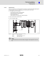
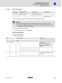
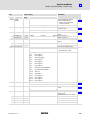
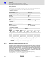
1
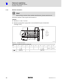
Ä.9Fqä
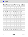
EDBCSXA064
.9Fq
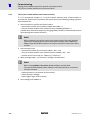
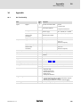
Operating Instructions
ECS
ECSEAxxx / ECSDAxxx / ECSCAxxx
Axis module ˘ "Application"
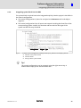
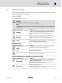
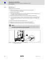
Please read these instructions before you start working!
Follow the enclosed safety instructions.
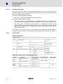
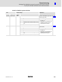
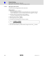
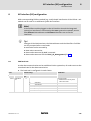
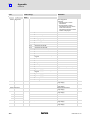
These Instructions are valid for ECSxA... axis modules as of version:
A
xxx
x
4
x
xxx XX
XX
XX
L
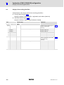
Input
Output
Design
Overload
E = standard panel−mounted unit, IP20
D = push−through technique (thermally separated)
C = cold−plate technique
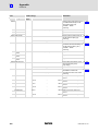
Type
ttttttttttt
1
Id.-No.
xxxxxxxx
Prod.-No.
yyyyyyyy
Ser.-No.
zzzz
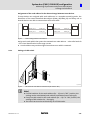
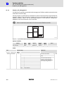
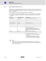
ATTENTION
A = "Application"
Peak current
Device is live up to
180s after removing
mains voltage
{ WARNING
}
032 = 32 A
048 = 48 A
064 = 64 A
L ´appareil est sous tension
pendant 180s après la coupure
de la tension réseau
EKZ ECSEAxxxC4BXXXXXVA02
B-SW
Parameter
A-SW
h.h
H.H
Application
004 = 4 A
008 = 8 A
016 = 16 A
Hans-Lenze-Straße1
D-31855 Aerzen
Made in Germany
2/PE DC a-aaa/aaaV
bb.b/bb.bA
3/PE AC c-ccc/cccV
dd.d/dd.dA
0-fffHz
ee.eA
1D74
Ind.
Conl.
Eq.
x
For detailed
information refer to
the Instruction Manual
ECS
Device type
Fieldbus interface
C = CAN system bus
Voltage class
4 = 400 V/500 V
Technical version
B = Standard
I = For IT systems
Variant
Hardware version
1A or higher
Version of operating software (B−SW)
8.0 or higher
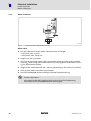
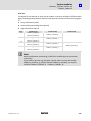
Tip!
Current documentation and software updates concerning Lenze products can be found on
the Internet in the "Services & Downloads" area under
http://www.Lenze.com
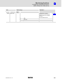
0Fig. 0Tab. 0
© 2008 Lenze Drive Systems GmbH, Hans−Lenze−Straße 1, D−31855 Aerzen
No part of this documentation may be reproduced or made accessible to third parties without written consent by Lenze Drive
Systems GmbH.
All information given in this documentation has been selected carefully and complies with the hardware and software described.
Nevertheless, discrepancies cannot be ruled out. We do not take any responsibility or liability for any damage that may occur. Necessary corrections will be included in subsequent editions.
2
EDBCSXA064 EN 2.0
ECSEA_003A
EDBCSXA064 EN 2.0
3
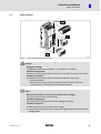
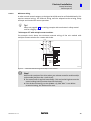
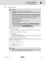
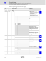
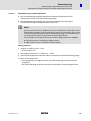
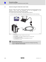
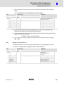
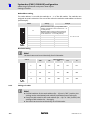
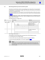
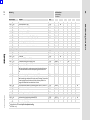
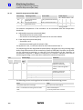
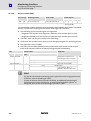
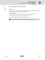
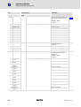
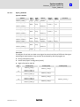
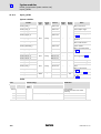
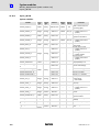
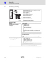
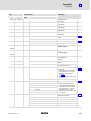
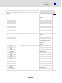
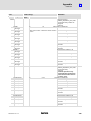
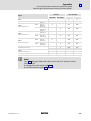
Scope of supply
Position
Description
Quantity
ECSA... axis module
1
Accessory kit with fixing material corresponding to the design ():
l "E" − standard panel−mounted unit
l "D" − push−through technique
l "C" − cold−plate technique
1
Mounting Instructions
1
Drilling jig
1
Functional earth conductor (only ECSDA...)
1
Note!
The ECSZA000X0B connector set must be ordered separately.
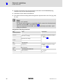
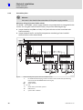
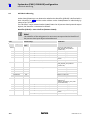
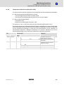
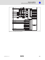
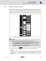
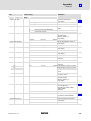
Connections and interfaces
Position
Description
X23
Connections
l DC−bus voltage
l PE
LEDs: Status and error display
x1
Automation interface (AIF) for
l operating module (keypad XT)
l Communication module
X2
PE connection of AIF
X3
Configuration of analog input
X4
CAN connection
l System bus (CAN)
CAN−AUX connection
l System bus (CAN)
Connections
l Low−voltage supply
l Digital inputs and outputs
l Analog input
l "Safe torque off" (formerly "safe standstill")
DIP switch
l CAN/CANaux node address
l CAN baud rate
X14
X6
S1
Detailed
information
56
78
68
79
64
67
68
69
161
X7
Resolver connection
86
X8
Encoder connection
l Incremental encoder (TTL encoder)
l Sin/cos encoder
87
X25
Connection of brake control
61
X24
Motor connection
60
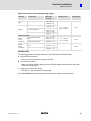
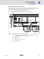
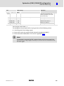
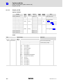
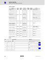
Status displays
LED
Red
Operating state
Check test
Green
Off
On
Controller enabled, no fault
Off
Blinking
Controller inhibited (CINH), switch−on inhibit
Code C0183
Blinking
Off
Trouble/fault (TRIP) is active
Code C0168/1
Blinking
On
Warning/FAIL−QSP is active
Code C0168/1
4
EDBCSXA064 EN 2.0
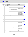
Contents
1
2
3
4
i
Preface and general information . . . . . . . . . . . . . . . . . . . . . . . . . . . . . . . . . . . . . . . . . . . .
13
1.1
About use these Operating Instructions . . . . . . . . . . . . . . . . . . . . . . . . . . . . . . . . . .
1.1.1
Conventions used in this Manual . . . . . . . . . . . . . . . . . . . . . . . . . . . . . . . .
1.1.2
Terminology used . . . . . . . . . . . . . . . . . . . . . . . . . . . . . . . . . . . . . . . . . . . . .
1.1.3
Structure of the system block descriptions . . . . . . . . . . . . . . . . . . . . . . . .
13
13
14
15
1.2
Features of the ECSxA axis module . . . . . . . . . . . . . . . . . . . . . . . . . . . . . . . . . . . . . .
15
1.3
Scope of supply . . . . . . . . . . . . . . . . . . . . . . . . . . . . . . . . . . . . . . . . . . . . . . . . . . . . . .
16
1.4
Legal regulations . . . . . . . . . . . . . . . . . . . . . . . . . . . . . . . . . . . . . . . . . . . . . . . . . . . . .
17
1.5
System block introduction . . . . . . . . . . . . . . . . . . . . . . . . . . . . . . . . . . . . . . . . . . . . .
1.5.1
System blocks ˘ principle . . . . . . . . . . . . . . . . . . . . . . . . . . . . . . . . . . . . . .
1.5.2
Node numbers . . . . . . . . . . . . . . . . . . . . . . . . . . . . . . . . . . . . . . . . . . . . . . .
1.5.3
Access via system variables . . . . . . . . . . . . . . . . . . . . . . . . . . . . . . . . . . . . .
1.5.4
Access via absolute addresses . . . . . . . . . . . . . . . . . . . . . . . . . . . . . . . . . .
1.5.5
Definition of the inputs/outputs . . . . . . . . . . . . . . . . . . . . . . . . . . . . . . . .
1.5.6
Integrating system blocks into the DDS . . . . . . . . . . . . . . . . . . . . . . . . . .
1.5.7
Signal types and scaling . . . . . . . . . . . . . . . . . . . . . . . . . . . . . . . . . . . . . . .
18
18
19
20
21
21
23
24
Safety instructions . . . . . . . . . . . . . . . . . . . . . . . . . . . . . . . . . . . . . . . . . . . . . . . . . . . . . . . . .
25
2.1
General safety and application notes for Lenze controllers . . . . . . . . . . . . . . . . . .
25
2.2
Residual hazards . . . . . . . . . . . . . . . . . . . . . . . . . . . . . . . . . . . . . . . . . . . . . . . . . . . . .
28
2.3
Safety instructions for the installation according to UL or UR . . . . . . . . . . . . . . . .
30
2.4
Definition of notes used . . . . . . . . . . . . . . . . . . . . . . . . . . . . . . . . . . . . . . . . . . . . . . .
31
Technical data . . . . . . . . . . . . . . . . . . . . . . . . . . . . . . . . . . . . . . . . . . . . . . . . . . . . . . . . . . . .
32
3.1
General data and operating conditions
.................................
32
3.2
Rated data . . . . . . . . . . . . . . . . . . . . . . . . . . . . . . . . . . . . . . . . . . . . . . . . . . . . . . . . . .
34
3.3
Current characteristics . . . . . . . . . . . . . . . . . . . . . . . . . . . . . . . . . . . . . . . . . . . . . . . .
3.3.1
Increased continuous current depending on the control factor . . . . . . .
3.3.2
Device protection by current derating . . . . . . . . . . . . . . . . . . . . . . . . . . . .
36
36
39
Mechanical installation . . . . . . . . . . . . . . . . . . . . . . . . . . . . . . . . . . . . . . . . . . . . . . . . . . . . .
40
4.1
Important notes . . . . . . . . . . . . . . . . . . . . . . . . . . . . . . . . . . . . . . . . . . . . . . . . . . . . . .
40
4.2
Mounting with fixing rails (standard installation) . . . . . . . . . . . . . . . . . . . . . . . . .
4.2.1
Dimensions . . . . . . . . . . . . . . . . . . . . . . . . . . . . . . . . . . . . . . . . . . . . . . . . . .
4.2.2
Mounting steps . . . . . . . . . . . . . . . . . . . . . . . . . . . . . . . . . . . . . . . . . . . . . .
41
41
42
4.3
Mounting with thermal separation (push−through technique) . . . . . . . . . . . . . . .
4.3.1
Dimensions . . . . . . . . . . . . . . . . . . . . . . . . . . . . . . . . . . . . . . . . . . . . . . . . . .
4.3.2
Mounting steps . . . . . . . . . . . . . . . . . . . . . . . . . . . . . . . . . . . . . . . . . . . . . .
43
44
46
4.4
Mounting in cold−plate design . . . . . . . . . . . . . . . . . . . . . . . . . . . . . . . . . . . . . . . . . .
4.4.1
Dimensions . . . . . . . . . . . . . . . . . . . . . . . . . . . . . . . . . . . . . . . . . . . . . . . . . .
4.4.2
Mounting steps . . . . . . . . . . . . . . . . . . . . . . . . . . . . . . . . . . . . . . . . . . . . . .
47
48
49
EDBCSXA064 EN 2.0
5
i
5
6
6
Contents
Electrical installation . . . . . . . . . . . . . . . . . . . . . . . . . . . . . . . . . . . . . . . . . . . . . . . . . . . . . . .
50
5.1
Electrical isolation . . . . . . . . . . . . . . . . . . . . . . . . . . . . . . . . . . . . . . . . . . . . . . . . . . . .
50
5.2
Installation according to EMC (installation of a CE−typical drive system) . . . . . . .
51
5.3
Power terminals . . . . . . . . . . . . . . . . . . . . . . . . . . . . . . . . . . . . . . . . . . . . . . . . . . . . . .
5.3.1
Connection to the DC bus (+UG, −UG) . . . . . . . . . . . . . . . . . . . . . . . . . . . .
5.3.2
Connection plans . . . . . . . . . . . . . . . . . . . . . . . . . . . . . . . . . . . . . . . . . . . . .
5.3.3
Motor connection . . . . . . . . . . . . . . . . . . . . . . . . . . . . . . . . . . . . . . . . . . . . .
5.3.4
Motor holding brake connection . . . . . . . . . . . . . . . . . . . . . . . . . . . . . . . .
5.3.5
Connection of an ECSxK... capacitor module (optional) . . . . . . . . . . . . . .
53
56
58
60
61
63
5.4
Control terminals . . . . . . . . . . . . . . . . . . . . . . . . . . . . . . . . . . . . . . . . . . . . . . . . . . . . .
5.4.1
Digital inputs and outputs . . . . . . . . . . . . . . . . . . . . . . . . . . . . . . . . . . . . .
5.4.2
Analog input . . . . . . . . . . . . . . . . . . . . . . . . . . . . . . . . . . . . . . . . . . . . . . . . .
5.4.3
Safe torque off . . . . . . . . . . . . . . . . . . . . . . . . . . . . . . . . . . . . . . . . . . . . . . .
64
67
68
69
5.5
Automation interface (AIF) . . . . . . . . . . . . . . . . . . . . . . . . . . . . . . . . . . . . . . . . . . . . .
78
5.6
Wiring of the system bus (CAN) . . . . . . . . . . . . . . . . . . . . . . . . . . . . . . . . . . . . . . . . .
79
5.7
Wiring of the feedback system . . . . . . . . . . . . . . . . . . . . . . . . . . . . . . . . . . . . . . . . .
5.7.1
Resolver connection . . . . . . . . . . . . . . . . . . . . . . . . . . . . . . . . . . . . . . . . . . .
5.7.2
Encoder connection . . . . . . . . . . . . . . . . . . . . . . . . . . . . . . . . . . . . . . . . . . .
5.7.3
Digital frequency input/output (encoder simulation) . . . . . . . . . . . . . . .
85
86
87
90
Commissioning . . . . . . . . . . . . . . . . . . . . . . . . . . . . . . . . . . . . . . . . . . . . . . . . . . . . . . . . . . .
92
6.1
Before you start . . . . . . . . . . . . . . . . . . . . . . . . . . . . . . . . . . . . . . . . . . . . . . . . . . . . . .
92
6.2
Commissioning steps (overview) . . . . . . . . . . . . . . . . . . . . . . . . . . . . . . . . . . . . . . . .
93
6.3
Carrying out basic settings with GDC . . . . . . . . . . . . . . . . . . . . . . . . . . . . . . . . . . . .
94
6.4
Setting of mains data . . . . . . . . . . . . . . . . . . . . . . . . . . . . . . . . . . . . . . . . . . . . . . . . .
6.4.1
Selecting the function of the charging current limitation . . . . . . . . . . . .
6.4.2
Setting the voltage thresholds . . . . . . . . . . . . . . . . . . . . . . . . . . . . . . . . . .
96
96
97
6.5
Entry of motor data for Lenze motors . . . . . . . . . . . . . . . . . . . . . . . . . . . . . . . . . . . .
98
6.6
Holding brake configuration . . . . . . . . . . . . . . . . . . . . . . . . . . . . . . . . . . . . . . . . . . .
100
6.7
Setting of the feedback system for position and speed control . . . . . . . . . . . . . . .
101
6.7.1
Resolver as position and speed encoder . . . . . . . . . . . . . . . . . . . . . . . . . .
101
6.7.2
TTL/sin/cos encoder without serial communication . . . . . . . . . . . . . . . .
104
6.7.3
TTL/sin/cos encoder as position encoder and resolver as speed encoder
107
6.7.4
Absolute value encoder as position and speed encoder . . . . . . . . . . . . .
110
6.7.5
Absolute value encoder as position encoder and resolver as speed encoder . . . .
114
6.8
Setting the polarity of digital inputs and outputs . . . . . . . . . . . . . . . . . . . . . . . . . .
118
6.9
Entry of machine parameters . . . . . . . . . . . . . . . . . . . . . . . . . . . . . . . . . . . . . . . . . . .
119
6.10 Controller enable . . . . . . . . . . . . . . . . . . . . . . . . . . . . . . . . . . . . . . . . . . . . . . . . . . . . .
120
6.11 Loading the Lenze setting . . . . . . . . . . . . . . . . . . . . . . . . . . . . . . . . . . . . . . . . . . . . . .
121
EDBCSXA064 EN 2.0
Contents
7
8
9
i
6.12 Operation with servo motors from other manufacturers . . . . . . . . . . . . . . . . . . . .
6.12.1 Entering motor data manually . . . . . . . . . . . . . . . . . . . . . . . . . . . . . . . . . .
6.12.2 Checking the direction of rotation of the motor feedback system . . . . .
6.12.3 Adjusting current controller . . . . . . . . . . . . . . . . . . . . . . . . . . . . . . . . . . . .
6.12.4 Effecting rotor position adjustment . . . . . . . . . . . . . . . . . . . . . . . . . . . . .
122
122
124
125
127
6.13 Optimising the drive behaviour after start . . . . . . . . . . . . . . . . . . . . . . . . . . . . . . . .
6.13.1 Speed controller adjustment . . . . . . . . . . . . . . . . . . . . . . . . . . . . . . . . . . . .
6.13.2 Adjustment of field controller and field weakening controller . . . . . . . .
6.13.3 Resolver adjustment . . . . . . . . . . . . . . . . . . . . . . . . . . . . . . . . . . . . . . . . . .
130
130
133
136
Parameter setting . . . . . . . . . . . . . . . . . . . . . . . . . . . . . . . . . . . . . . . . . . . . . . . . . . . . . . . . .
137
7.1
General information
.................................................
137
7.2
Parameter setting with "Global Drive Control" (GDC) . . . . . . . . . . . . . . . . . . . . . . .
138
7.3
Parameter setting with the XT EMZ9371BC keypad . . . . . . . . . . . . . . . . . . . . . . . .
7.3.1
Connecting the keypad . . . . . . . . . . . . . . . . . . . . . . . . . . . . . . . . . . . . . . . .
7.3.2
Description of the display elements . . . . . . . . . . . . . . . . . . . . . . . . . . . . . .
7.3.3
Description of the function keys . . . . . . . . . . . . . . . . . . . . . . . . . . . . . . . . .
7.3.4
Changing and saving parameters . . . . . . . . . . . . . . . . . . . . . . . . . . . . . . . .
7.3.5
Menu structure . . . . . . . . . . . . . . . . . . . . . . . . . . . . . . . . . . . . . . . . . . . . . . .
139
139
140
141
142
143
AIF interface (X1) configuration . . . . . . . . . . . . . . . . . . . . . . . . . . . . . . . . . . . . . . . . . . . . . .
145
8.1
CAN baud rate . . . . . . . . . . . . . . . . . . . . . . . . . . . . . . . . . . . . . . . . . . . . . . . . . . . . . . .
145
8.2
CAN boot up (AIF) . . . . . . . . . . . . . . . . . . . . . . . . . . . . . . . . . . . . . . . . . . . . . . . . . . . .
146
8.3
Node address (Node ID) . . . . . . . . . . . . . . . . . . . . . . . . . . . . . . . . . . . . . . . . . . . . . . .
147
8.4
Identifiers of the process data objects . . . . . . . . . . . . . . . . . . . . . . . . . . . . . . . . . . .
8.4.1
Individual identifier assignment . . . . . . . . . . . . . . . . . . . . . . . . . . . . . . . .
8.4.2
Display of the identifier set . . . . . . . . . . . . . . . . . . . . . . . . . . . . . . . . . . . . .
148
148
149
8.5
Cycle time (XCAN1_OUT ... XCAN3_OUT) . . . . . . . . . . . . . . . . . . . . . . . . . . . . . . . . .
150
8.6
Synchronisation . . . . . . . . . . . . . . . . . . . . . . . . . . . . . . . . . . . . . . . . . . . . . . . . . . . . . .
8.6.1
XCAN sync response . . . . . . . . . . . . . . . . . . . . . . . . . . . . . . . . . . . . . . . . . . .
8.6.2
XCAN sync identifier . . . . . . . . . . . . . . . . . . . . . . . . . . . . . . . . . . . . . . . . . .
8.6.3
XCAN Sync Tx transmission cycle . . . . . . . . . . . . . . . . . . . . . . . . . . . . . . . .
152
152
152
153
8.7
Reset node . . . . . . . . . . . . . . . . . . . . . . . . . . . . . . . . . . . . . . . . . . . . . . . . . . . . . . . . . .
153
8.8
Monitoring . . . . . . . . . . . . . . . . . . . . . . . . . . . . . . . . . . . . . . . . . . . . . . . . . . . . . . . . . .
8.8.1
Time monitoring for XCAN1_IN ... XCAN3_IN . . . . . . . . . . . . . . . . . . . . . .
8.8.2
Bus off . . . . . . . . . . . . . . . . . . . . . . . . . . . . . . . . . . . . . . . . . . . . . . . . . . . . . .
154
154
155
8.9
Diagnostics . . . . . . . . . . . . . . . . . . . . . . . . . . . . . . . . . . . . . . . . . . . . . . . . . . . . . . . . . .
8.9.1
Operating status of CAN interface . . . . . . . . . . . . . . . . . . . . . . . . . . . . . . .
157
157
System bus (CAN / CAN−AUX) configuration . . . . . . . . . . . . . . . . . . . . . . . . . . . . . . . . . . .
159
9.1
159
Setting the CAN node address and baud rate . . . . . . . . . . . . . . . . . . . . . . . . . . . . .
EDBCSXA064 EN 2.0
7
i
10
11
8
Contents
9.2
Addressing of parameter and process data objects . . . . . . . . . . . . . . . . . . . . . . . .
9.2.1
Settings via DIP switch . . . . . . . . . . . . . . . . . . . . . . . . . . . . . . . . . . . . . . . .
9.2.2
Settings via codes . . . . . . . . . . . . . . . . . . . . . . . . . . . . . . . . . . . . . . . . . . . . .
160
161
162
9.3
Individual addressing . . . . . . . . . . . . . . . . . . . . . . . . . . . . . . . . . . . . . . . . . . . . . . . . .
164
9.4
Display of the resulting identifiers . . . . . . . . . . . . . . . . . . . . . . . . . . . . . . . . . . . . . .
166
9.5
Determining the boot−up master for the drive system . . . . . . . . . . . . . . . . . . . . . .
167
9.6
Setting the boot−up time/cycle time . . . . . . . . . . . . . . . . . . . . . . . . . . . . . . . . . . . .
168
9.7
Node guarding . . . . . . . . . . . . . . . . . . . . . . . . . . . . . . . . . . . . . . . . . . . . . . . . . . . . . .
169
9.8
CANSync (CAN bus synchronisation) . . . . . . . . . . . . . . . . . . . . . . . . . . . . . . . . . . . . .
9.8.1
CAN sync response . . . . . . . . . . . . . . . . . . . . . . . . . . . . . . . . . . . . . . . . . . . .
9.8.2
CAN sync identifiers . . . . . . . . . . . . . . . . . . . . . . . . . . . . . . . . . . . . . . . . . . .
9.8.3
CAN sync Tx transmission cycle . . . . . . . . . . . . . . . . . . . . . . . . . . . . . . . . .
171
171
171
172
9.9
Reset node . . . . . . . . . . . . . . . . . . . . . . . . . . . . . . . . . . . . . . . . . . . . . . . . . . . . . . . . . .
173
9.10 System bus management . . . . . . . . . . . . . . . . . . . . . . . . . . . . . . . . . . . . . . . . . . . . . .
174
9.11 Mapping of indices to codes . . . . . . . . . . . . . . . . . . . . . . . . . . . . . . . . . . . . . . . . . . . .
175
9.12 Remote parameterisation (gateway function) . . . . . . . . . . . . . . . . . . . . . . . . . . . . .
177
9.13 Diagnostics codes . . . . . . . . . . . . . . . . . . . . . . . . . . . . . . . . . . . . . . . . . . . . . . . . . . . .
9.13.1 Bus status (C0359/C2459) . . . . . . . . . . . . . . . . . . . . . . . . . . . . . . . . . . . . .
9.13.2 Telegram counter (C0360/2460) . . . . . . . . . . . . . . . . . . . . . . . . . . . . . . . .
9.13.3 Bus load (C0361/2461) . . . . . . . . . . . . . . . . . . . . . . . . . . . . . . . . . . . . . . . .
178
178
179
180
Diagnostics . . . . . . . . . . . . . . . . . . . . . . . . . . . . . . . . . . . . . . . . . . . . . . . . . . . . . . . . . . . . . . .
181
10.1 Diagnostics with Global Drive Control (GDC) . . . . . . . . . . . . . . . . . . . . . . . . . . . . . .
181
10.2 Diagnostics with Global Drive Oscilloscope (GDO) . . . . . . . . . . . . . . . . . . . . . . . . .
182
10.3 Diagnostics with the XT EMZ9371BC keypad . . . . . . . . . . . . . . . . . . . . . . . . . . . . . .
183
Monitoring functions . . . . . . . . . . . . . . . . . . . . . . . . . . . . . . . . . . . . . . . . . . . . . . . . . . . . . . .
184
11.1 Overview of monitoring functions . . . . . . . . . . . . . . . . . . . . . . . . . . . . . . . . . . . . . . .
184
EDBCSXA064 EN 2.0
Contents
12
13
i
11.2 Configuring monitoring functions . . . . . . . . . . . . . . . . . . . . . . . . . . . . . . . . . . . . . . .
11.2.1 Responses . . . . . . . . . . . . . . . . . . . . . . . . . . . . . . . . . . . . . . . . . . . . . . . . . . .
11.2.2 Monitoring times for process data input objects . . . . . . . . . . . . . . . . . . .
11.2.3 Time−out with activated remote parameterisation . . . . . . . . . . . . . . . . .
11.2.4 Short circuit monitoring (OC1) . . . . . . . . . . . . . . . . . . . . . . . . . . . . . . . . . .
11.2.5 Earth fault monitoring (OC2) . . . . . . . . . . . . . . . . . . . . . . . . . . . . . . . . . . .
11.2.6 Motor temperature (OH3, OH7) . . . . . . . . . . . . . . . . . . . . . . . . . . . . . . . . .
11.2.7 Heatsink temperature (OH, OH4) . . . . . . . . . . . . . . . . . . . . . . . . . . . . . . . .
11.2.8 Temperature inside the controller (OH1, OH5) . . . . . . . . . . . . . . . . . . . . .
11.2.9 Thermal sensor function monitoring (H10, H11) . . . . . . . . . . . . . . . . . . .
11.2.10 Current load of controller (I x t monitoring: OC5, OC7) . . . . . . . . . . . . . .
11.2.11 Current load of motor (I2 x t monitoring: OC6, OC8) . . . . . . . . . . . . . . . .
11.2.12 DC−bus voltage (OU, LU) . . . . . . . . . . . . . . . . . . . . . . . . . . . . . . . . . . . . . . .
11.2.13 Voltage supply of the control electronics (U15) . . . . . . . . . . . . . . . . . . . .
11.2.14 Motor phases (LP1) . . . . . . . . . . . . . . . . . . . . . . . . . . . . . . . . . . . . . . . . . . . .
11.2.15 Resolver cable (Sd2) . . . . . . . . . . . . . . . . . . . . . . . . . . . . . . . . . . . . . . . . . . .
11.2.16 Motor temperature sensor (Sd6) . . . . . . . . . . . . . . . . . . . . . . . . . . . . . . . .
11.2.17 Absolute value encoder monitoring (Sd7) . . . . . . . . . . . . . . . . . . . . . . . . .
11.2.18 Sin/cos encoder (Sd8) . . . . . . . . . . . . . . . . . . . . . . . . . . . . . . . . . . . . . . . . .
11.2.19 Speed not within tolerance margin (nErr) . . . . . . . . . . . . . . . . . . . . . . . . .
11.2.20 Maximum speed exceeded (NMAX) . . . . . . . . . . . . . . . . . . . . . . . . . . . . . .
11.2.21 Rotor position adjustment (PL) . . . . . . . . . . . . . . . . . . . . . . . . . . . . . . . . .
189
189
191
192
193
193
193
196
197
198
198
201
202
204
205
206
207
207
208
210
211
212
Troubleshooting and fault elimination . . . . . . . . . . . . . . . . . . . . . . . . . . . . . . . . . . . . . . .
213
12.1 Fault analysis . . . . . . . . . . . . . . . . . . . . . . . . . . . . . . . . . . . . . . . . . . . . . . . . . . . . . . . .
12.1.1 Fault analysis via the LED display . . . . . . . . . . . . . . . . . . . . . . . . . . . . . . . .
12.1.2 Fault analysis with keypad XT EMZ9371BC . . . . . . . . . . . . . . . . . . . . . . . .
12.1.3 Fault analysis with the history buffer . . . . . . . . . . . . . . . . . . . . . . . . . . . .
12.1.4 Fault analysis via LECOM status words (C0150/C0155) . . . . . . . . . . . . .
213
213
213
213
215
12.2 Malfunction of the drive . . . . . . . . . . . . . . . . . . . . . . . . . . . . . . . . . . . . . . . . . . . . . . .
217
12.3 System error messages . . . . . . . . . . . . . . . . . . . . . . . . . . . . . . . . . . . . . . . . . . . . . . . .
12.3.1 Overview of system error messages, error sources and reactions . . . . .
12.3.2 Causes and remedies . . . . . . . . . . . . . . . . . . . . . . . . . . . . . . . . . . . . . . . . . .
12.3.3 Resetting system error messages . . . . . . . . . . . . . . . . . . . . . . . . . . . . . . . .
218
218
222
229
System blocks . . . . . . . . . . . . . . . . . . . . . . . . . . . . . . . . . . . . . . . . . . . . . . . . . . . . . . . . . . . . .
230
13.1 AIF_IO_Management (node number 161) . . . . . . . . . . . . . . . . . . . . . . . . . . . . . . . .
13.1.1 Inputs_AIF_Management . . . . . . . . . . . . . . . . . . . . . . . . . . . . . . . . . . . . . .
13.1.2 Outputs_AIF_Management . . . . . . . . . . . . . . . . . . . . . . . . . . . . . . . . . . . .
231
231
234
13.2 AIF1_IO_AutomationInterface (node number 41) . . . . . . . . . . . . . . . . . . . . . . . . . .
13.2.1 Inputs_AIF1 . . . . . . . . . . . . . . . . . . . . . . . . . . . . . . . . . . . . . . . . . . . . . . . . . .
13.2.2 Outputs_AIF1 . . . . . . . . . . . . . . . . . . . . . . . . . . . . . . . . . . . . . . . . . . . . . . . .
235
235
240
EDBCSXA064 EN 2.0
9
i
10
Contents
13.3 AIF2_IO_AutomationInterface (node number 42) . . . . . . . . . . . . . . . . . . . . . . . . . .
13.3.1 Inputs_AIF2 . . . . . . . . . . . . . . . . . . . . . . . . . . . . . . . . . . . . . . . . . . . . . . . . . .
13.3.2 Outputs_AIF2 . . . . . . . . . . . . . . . . . . . . . . . . . . . . . . . . . . . . . . . . . . . . . . . .
243
243
245
13.4 AIF3_IO_AutomationInterface (node number 43) . . . . . . . . . . . . . . . . . . . . . . . . . .
13.4.1 Inputs_AIF3 . . . . . . . . . . . . . . . . . . . . . . . . . . . . . . . . . . . . . . . . . . . . . . . . . .
13.4.2 Outputs_AIF3 . . . . . . . . . . . . . . . . . . . . . . . . . . . . . . . . . . . . . . . . . . . . . . . .
247
247
249
13.5 ANALOG1_IO (node number 11) . . . . . . . . . . . . . . . . . . . . . . . . . . . . . . . . . . . . . . . .
13.5.1 Inputs_ANALOG1 (analog input) . . . . . . . . . . . . . . . . . . . . . . . . . . . . . . . .
251
251
13.6 CAN_Management (node number 101) . . . . . . . . . . . . . . . . . . . . . . . . . . . . . . . . . .
13.6.1 Inputs_CAN_Management . . . . . . . . . . . . . . . . . . . . . . . . . . . . . . . . . . . . .
13.6.2 Outputs_CAN_Management . . . . . . . . . . . . . . . . . . . . . . . . . . . . . . . . . . .
13.6.3 Executing a reset node . . . . . . . . . . . . . . . . . . . . . . . . . . . . . . . . . . . . . . . . .
13.6.4 Define instant of transmission for CAN2_OUT/CAN3_OUT . . . . . . . . . .
13.6.5 Status messages . . . . . . . . . . . . . . . . . . . . . . . . . . . . . . . . . . . . . . . . . . . . . .
253
254
254
255
255
256
13.7 CAN_Synchronization (node number 102) . . . . . . . . . . . . . . . . . . . . . . . . . . . . . . . .
13.7.1 Axis synchronisation via CAN bus interface . . . . . . . . . . . . . . . . . . . . . . .
13.7.2 Axis synchronisation via terminal X6/DI1 . . . . . . . . . . . . . . . . . . . . . . . . .
257
261
262
13.8 CAN1_IO (node number 31) . . . . . . . . . . . . . . . . . . . . . . . . . . . . . . . . . . . . . . . . . . . .
13.8.1 Inputs_CAN1 . . . . . . . . . . . . . . . . . . . . . . . . . . . . . . . . . . . . . . . . . . . . . . . . .
13.8.2 Outputs_CAN1 . . . . . . . . . . . . . . . . . . . . . . . . . . . . . . . . . . . . . . . . . . . . . . .
263
267
268
13.9 CAN2_IO (node number 32) . . . . . . . . . . . . . . . . . . . . . . . . . . . . . . . . . . . . . . . . . . . .
13.9.1 Inputs_CAN2 . . . . . . . . . . . . . . . . . . . . . . . . . . . . . . . . . . . . . . . . . . . . . . . . .
13.9.2 Outputs_CAN2 . . . . . . . . . . . . . . . . . . . . . . . . . . . . . . . . . . . . . . . . . . . . . . .
269
272
273
13.10 CAN3_IO (node number 33) . . . . . . . . . . . . . . . . . . . . . . . . . . . . . . . . . . . . . . . . . . . .
13.10.1 Inputs_CAN3 . . . . . . . . . . . . . . . . . . . . . . . . . . . . . . . . . . . . . . . . . . . . . . . . .
13.10.2 Outputs_CAN3 . . . . . . . . . . . . . . . . . . . . . . . . . . . . . . . . . . . . . . . . . . . . . . .
274
277
278
13.11 CANaux_Management (node number 111) . . . . . . . . . . . . . . . . . . . . . . . . . . . . . . .
13.11.1 Inputs_CANaux_Management . . . . . . . . . . . . . . . . . . . . . . . . . . . . . . . . . .
13.11.2 Outputs_CANaux_Management . . . . . . . . . . . . . . . . . . . . . . . . . . . . . . . .
13.11.3 Executing a reset node . . . . . . . . . . . . . . . . . . . . . . . . . . . . . . . . . . . . . . . . .
13.11.4 Define instant of transmission for CANaux2_OUT/CANaux3_OUT . . . .
13.11.5 Status messages . . . . . . . . . . . . . . . . . . . . . . . . . . . . . . . . . . . . . . . . . . . . . .
279
279
280
280
280
281
13.12 CANaux1_IO (node number 34) . . . . . . . . . . . . . . . . . . . . . . . . . . . . . . . . . . . . . . . . .
13.12.1 Inputs_CANaux1 . . . . . . . . . . . . . . . . . . . . . . . . . . . . . . . . . . . . . . . . . . . . .
13.12.2 Outputs_CANaux1 . . . . . . . . . . . . . . . . . . . . . . . . . . . . . . . . . . . . . . . . . . . .
282
285
286
13.13 CANaux2_IO (node number 35) . . . . . . . . . . . . . . . . . . . . . . . . . . . . . . . . . . . . . . . . .
13.13.1 Inputs_CANaux2 . . . . . . . . . . . . . . . . . . . . . . . . . . . . . . . . . . . . . . . . . . . . .
13.13.2 Outputs_CANaux2 . . . . . . . . . . . . . . . . . . . . . . . . . . . . . . . . . . . . . . . . . . . .
288
291
292
13.14 CANaux3_IO (node number 36) . . . . . . . . . . . . . . . . . . . . . . . . . . . . . . . . . . . . . . . . .
13.14.1 Inputs_CANaux3 . . . . . . . . . . . . . . . . . . . . . . . . . . . . . . . . . . . . . . . . . . . . .
13.14.2 Outputs_CANaux3 . . . . . . . . . . . . . . . . . . . . . . . . . . . . . . . . . . . . . . . . . . . .
293
296
297
EDBCSXA064 EN 2.0
Contents
14
i
13.15 DCTRL_DriveControl (node number 121) . . . . . . . . . . . . . . . . . . . . . . . . . . . . . . . . .
13.15.1 Inputs_DCTRL . . . . . . . . . . . . . . . . . . . . . . . . . . . . . . . . . . . . . . . . . . . . . . . .
13.15.2 Outputs_DCTRL . . . . . . . . . . . . . . . . . . . . . . . . . . . . . . . . . . . . . . . . . . . . . .
13.15.3 Quick stop (QSP) . . . . . . . . . . . . . . . . . . . . . . . . . . . . . . . . . . . . . . . . . . . . . .
13.15.4 Operation inhibit (DISABLE) . . . . . . . . . . . . . . . . . . . . . . . . . . . . . . . . . . . .
13.15.5 Controller inhibit (CINH) . . . . . . . . . . . . . . . . . . . . . . . . . . . . . . . . . . . . . . .
13.15.6 Setting TRIP (TRIP−SET) . . . . . . . . . . . . . . . . . . . . . . . . . . . . . . . . . . . . . . . . .
13.15.7 Resetting TRIP (TRIP−RESET) . . . . . . . . . . . . . . . . . . . . . . . . . . . . . . . . . . . . .
13.15.8 Display of digital status signals . . . . . . . . . . . . . . . . . . . . . . . . . . . . . . . . .
13.15.9 TRIP status (DCTRL_bExternalFault_b) . . . . . . . . . . . . . . . . . . . . . . . . . . .
13.15.10 Transfer of the status/control word via AIF . . . . . . . . . . . . . . . . . . . . . . . .
298
300
302
303
303
304
304
305
305
306
307
13.16 DFIN_IO_DigitalFrequency (node number 21) . . . . . . . . . . . . . . . . . . . . . . . . . . . . .
13.16.1 Inputs_DFIN . . . . . . . . . . . . . . . . . . . . . . . . . . . . . . . . . . . . . . . . . . . . . . . . .
309
309
13.17 DFOUT_IO_DigitalFrequency (node number 22) . . . . . . . . . . . . . . . . . . . . . . . . . . .
13.17.1 Inputs_DFOUT / Outputs_DFOUT . . . . . . . . . . . . . . . . . . . . . . . . . . . . . . .
316
316
13.18 DIGITAL_IO (node number 1) . . . . . . . . . . . . . . . . . . . . . . . . . . . . . . . . . . . . . . . . . . .
13.18.1 Inputs_DIGITAL (digital inputs) . . . . . . . . . . . . . . . . . . . . . . . . . . . . . . . . .
13.18.2 Outputs_DIGITAL (digital outputs) . . . . . . . . . . . . . . . . . . . . . . . . . . . . . .
321
321
323
13.19 FCODE_FreeCode (node number 141) . . . . . . . . . . . . . . . . . . . . . . . . . . . . . . . . . . . .
325
13.20 MCTRL_MotorControl (node number 131) . . . . . . . . . . . . . . . . . . . . . . . . . . . . . . . .
13.20.1 Inputs_MCTRL . . . . . . . . . . . . . . . . . . . . . . . . . . . . . . . . . . . . . . . . . . . . . . .
13.20.2 Outputs_MCTRL . . . . . . . . . . . . . . . . . . . . . . . . . . . . . . . . . . . . . . . . . . . . . .
13.20.3 Torque setpoint / additional torque setpoint . . . . . . . . . . . . . . . . . . . . . .
13.20.4 Torque limitation . . . . . . . . . . . . . . . . . . . . . . . . . . . . . . . . . . . . . . . . . . . . .
13.20.5 Setting maximum speed . . . . . . . . . . . . . . . . . . . . . . . . . . . . . . . . . . . . . . .
13.20.6 Speed setpoint limitation . . . . . . . . . . . . . . . . . . . . . . . . . . . . . . . . . . . . . .
13.20.7 Torque control with speed limitation . . . . . . . . . . . . . . . . . . . . . . . . . . . .
13.20.8 Parameterising phase controllers . . . . . . . . . . . . . . . . . . . . . . . . . . . . . . . .
13.20.9 Quick stop (QSP) . . . . . . . . . . . . . . . . . . . . . . . . . . . . . . . . . . . . . . . . . . . . . .
13.20.10 Manual field weakening . . . . . . . . . . . . . . . . . . . . . . . . . . . . . . . . . . . . . . .
13.20.11 Switching frequency changeover . . . . . . . . . . . . . . . . . . . . . . . . . . . . . . . .
13.20.12 Touch probe (TP) . . . . . . . . . . . . . . . . . . . . . . . . . . . . . . . . . . . . . . . . . . . . . .
13.20.13 Adjusting the motor data . . . . . . . . . . . . . . . . . . . . . . . . . . . . . . . . . . . . . .
13.20.14 Monitoring . . . . . . . . . . . . . . . . . . . . . . . . . . . . . . . . . . . . . . . . . . . . . . . . . .
329
330
332
333
334
335
335
336
336
337
338
338
339
341
344
13.21 OSC_Oscilloscope (node number 60) . . . . . . . . . . . . . . . . . . . . . . . . . . . . . . . . . . . .
346
13.22 SYSTEM_FLAGS (system flags, node number 151) . . . . . . . . . . . . . . . . . . . . . . . . . .
13.22.1 Inputs SYSTEM_FLAGS . . . . . . . . . . . . . . . . . . . . . . . . . . . . . . . . . . . . . . . . .
13.22.2 Outputs SYSTEM_FLAGS . . . . . . . . . . . . . . . . . . . . . . . . . . . . . . . . . . . . . . .
347
347
348
Appendix . . . . . . . . . . . . . . . . . . . . . . . . . . . . . . . . . . . . . . . . . . . . . . . . . . . . . . . . . . . . . . . .
349
14.1 PLC functionality . . . . . . . . . . . . . . . . . . . . . . . . . . . . . . . . . . . . . . . . . . . . . . . . . . . . .
349
14.2 Extendability / networking . . . . . . . . . . . . . . . . . . . . . . . . . . . . . . . . . . . . . . . . . . . . .
350
EDBCSXA064 EN 2.0
11
i
15
12
Contents
14.3 Memories . . . . . . . . . . . . . . . . . . . . . . . . . . . . . . . . . . . . . . . . . . . . . . . . . . . . . . . . . . .
14.3.1 Retain memory . . . . . . . . . . . . . . . . . . . . . . . . . . . . . . . . . . . . . . . . . . . . . . .
14.3.2 Persistent memory . . . . . . . . . . . . . . . . . . . . . . . . . . . . . . . . . . . . . . . . . . . .
14.3.3 Download of various data items . . . . . . . . . . . . . . . . . . . . . . . . . . . . . . . .
14.3.4 Temporary codes . . . . . . . . . . . . . . . . . . . . . . . . . . . . . . . . . . . . . . . . . . . . .
14.3.5 RAM memory access via codes . . . . . . . . . . . . . . . . . . . . . . . . . . . . . . . . . .
351
351
351
354
355
356
14.4 System program organisation units . . . . . . . . . . . . . . . . . . . . . . . . . . . . . . . . . . . . .
358
14.5 Code list . . . . . . . . . . . . . . . . . . . . . . . . . . . . . . . . . . . . . . . . . . . . . . . . . . . . . . . . . . . .
359
14.6 Table of attributes . . . . . . . . . . . . . . . . . . . . . . . . . . . . . . . . . . . . . . . . . . . . . . . . . . . .
403
14.7 General information about the system bus (CAN) . . . . . . . . . . . . . . . . . . . . . . . . . .
14.7.1 Structure of the CAN data telegram . . . . . . . . . . . . . . . . . . . . . . . . . . . . . .
14.7.2 Communication phases of the CAN network (NMT) . . . . . . . . . . . . . . . .
14.7.3 Process data transfer . . . . . . . . . . . . . . . . . . . . . . . . . . . . . . . . . . . . . . . . . .
14.7.4 Parameter data transfer . . . . . . . . . . . . . . . . . . . . . . . . . . . . . . . . . . . . . . .
14.7.5 Addressing of the parameter and process data objects . . . . . . . . . . . . . .
411
411
412
414
421
426
14.8 Overview of accessories . . . . . . . . . . . . . . . . . . . . . . . . . . . . . . . . . . . . . . . . . . . . . . .
14.8.1 Connector sets . . . . . . . . . . . . . . . . . . . . . . . . . . . . . . . . . . . . . . . . . . . . . . .
14.8.2 Shield mounting kit . . . . . . . . . . . . . . . . . . . . . . . . . . . . . . . . . . . . . . . . . . .
14.8.3 Power supply modules . . . . . . . . . . . . . . . . . . . . . . . . . . . . . . . . . . . . . . . . .
14.8.4 Capacitor modules . . . . . . . . . . . . . . . . . . . . . . . . . . . . . . . . . . . . . . . . . . . .
14.8.5 Components for operation and communication . . . . . . . . . . . . . . . . . . .
14.8.6 Brake resistor . . . . . . . . . . . . . . . . . . . . . . . . . . . . . . . . . . . . . . . . . . . . . . . .
14.8.7 Mains fuses . . . . . . . . . . . . . . . . . . . . . . . . . . . . . . . . . . . . . . . . . . . . . . . . . .
14.8.8 Mains chokes . . . . . . . . . . . . . . . . . . . . . . . . . . . . . . . . . . . . . . . . . . . . . . . .
14.8.9 RFI filters . . . . . . . . . . . . . . . . . . . . . . . . . . . . . . . . . . . . . . . . . . . . . . . . . . . .
14.8.10 Motors . . . . . . . . . . . . . . . . . . . . . . . . . . . . . . . . . . . . . . . . . . . . . . . . . . . . . .
428
428
428
428
428
429
429
431
431
432
432
Index . . . . . . . . . . . . . . . . . . . . . . . . . . . . . . . . . . . . . . . . . . . . . . . . . . . . . . . . . . . . . . . . . . . .
433
EDBCSXA064 EN 2.0
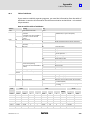
Preface and general information
1
About use these Operating Instructions
Conventions used in this Manual
1
Preface and general information
1.1
About use these Operating Instructions
These Operating Instructions will assist you in connecting and commissioning the ECSxA...
axis modules.
They contain safety instructions which must be observed!
All persons working on and with the ECSxA... axis modules must have the Operating
Instructions available and must observe the information and notes relevant for their work.
The Operating Instructions must always be in a complete and perfectly readable state.
1.1.1
Conventions used in this Manual
This Manual uses the following conventions to distinguish between different types of
information:
Information type
System block name
System block variable identifier
Print
(in the descriptive text)
bold
italics
Example
The SB DIGITAL_IO...
The input DIGIN_bIn1_b...
Further information ...
about the conventions used for the Lenze variable identifiers, system blocks,
function blocks, and functions can be found in the appendix of the DDS online
documentation "Introduction to IEC 61131−3 programming".
The compliance with these conventions ensures uniform and universal
labelling and makes reading PLC programs easier.
EDBCSXA064 EN 2.0
13
1
Preface and general information
About use these Operating Instructions
Terminology used
1.1.2
14
Terminology used
Term
In the following text used for
Power supply module
ECSxE...power supply module
ECSxE...
Any power supply module of the ECS series
Capacitor module
ECSxK...capacitor module
ECSxK...
Any capacitor module of the ECS series
Axis module
Controller
ECSxA... axis module
ECSxS...
ECSxP...
ECSxM...
ECSxA ...
Any axis module of the ECS series:
l ECSxS... "Speed and Torque" application
l ECSxP... "Posi and Shaft" application
l ECSxM... "Motion" application
l ECSxA... − "Application"
Drive system
Drive systems with:
l ECSxS... / ECSxP... / ECSxM... / ECSxA... axis modules
l ECSxE... power supply modules
l ECSxK... capacitor modules
l Other Lenze drive components
24 V supply
Low−voltage supply
Voltage supply
l of the control card, voltage range 20 ... 30 V DC (±0 V)
l of the "safe torque off"(formerly "safe standstill"), voltage range
18 ... 30 V DC (±0 V)
l of the motor holding brake, voltage range 23 ... 30 V DC (±0 V)
AIF
Automation InterFace
Cxxxx/y
Subcode y of code Cxxxx (e. g. C0470/3 = subcode 3 of code C0470)
Xk/y
Terminal y on plug connector Xk (e. g. X6/B+ = terminal B+ on plug connector X6)
DDS
Drive PLC Developer Studio
FB
Function block
GDC
Global Drive Control (parameter setting program from Lenze)
SB
System block
System bus (CAN)
Lenze standard bus system based on CANopen for
l communication with a higher−level master system or further controllers
l parameter setting and diagnostics.
EDBCSXA064 EN 2.0
Preface and general information
1
Features of the ECSxA
Terminology used
1.1.3
Structure of the system block descriptions
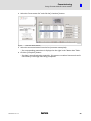
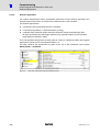
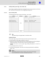
All system block descriptions contained in this Manual have the same structure:
Headline with SB identifier
SB function and node number
Brief description of the SB and its most important
features
Graph including all corresponding system variables
l Input variables
l Output variables
Table giving information about input and output
variables:
l Identifier
l Data type
l Signal type
l Address
l Display code
l Display format
l Information
l Detailed functional description of the SB
l Code description
1.2
Features of the ECSxA axis module
ƒ
Safety function "safe torque off" (formerly "safe standstill")
ƒ
Double CAN ON BOARD:
– CAN bus interface X4 "CAN" (PDO1, sync−based)
– CAN bus interface X14 "CAN−AUX"
ƒ
Supported feedback systems:
– Resolver with and without position storage
– Encoder (incremental encoder (TTL encoder), sin/cos encoder)
ƒ
Commissioning and parameter setting with the Lenze parameter setting and
operating program "Global Drive Control" (GDC)
EDBCSXA064 EN 2.0
15
1
Preface and general information
Scope of supply
Terminology used
1.3
Scope of supply
The scope of supply of the ECSxA... axis module includes:
ƒ
Standard device
ƒ
Accessory kit with fixings according to the design:
– "E" − panel−mounted device
– "D" − push−through technique
– "C" − cold−plate technique
ƒ
Mounting Instructions
ƒ
Drilling jig
ƒ
Functional earth conductor (only ECSDA...)
Accessories
The appendix includes information on the following accessories: (
428).
16
ƒ
Connector sets for
– power supply modules: ECSZE000X0B
– capacitor modules: ECSZK000X0B
– axis modules: ECSZA000X0B
ƒ
ECSZS000X0B001 shield mounting kit (EMC accessories)
ƒ
Communication modules for the automation interface (AIF)
ƒ
ECSxE...power supply module
ƒ
ECSxK... capacitor module
ƒ
Brake resistors
ƒ
Mains fuses
ƒ
Mains chokes
ƒ
RFI filters
ƒ
Motors
EDBCSXA064 EN 2.0
Preface and general information
1
Legal regulations
Terminology used
1.4
Legal regulations
Identification
Nameplate
Lenze controllers are
unambiguously designated by the
contents of the nameplate.
Application as
directed
ECSxA... axis modules
l must only be operated under the conditions prescribed in these instructions.
l are components
– for open and closed loop control of variable speed drives with PM synchronous motors and asynchronous
motors.
– for installation in a machine.
– for assembly with other components to form a machine.
l are electrical equipment for the installation in control cabinets or similar closed operating areas.
l comply with the protective requirements of the EC Low−Voltage Directive.
l are not machines for the purpose of the EC Machinery Directive.
l are not to be used as domestic appliances, but for industrial purposes only.
Drive systems with ECSxA... axis modules
l comply with the EC Directive "Electromagnetic compatibility" if they are installed according to the guidelines
of CE−typical drive systems.
l can be used
– at public and non−public mains.
– in industrial premises.
l The user is responsible for the compliance of his application with the EC directives.
Any other use shall be deemed inappropriate!
Liability
l
l
l
Warranty
l
l
l
EDBCSXA064 EN 2.0
CE identification
Conforms to the EC Low−Voltage
Directive
Manufacturer
Lenze Drive Systems GmbH
PO box 10 13 52
D−31763 Hameln
The information, data and notes in these instructions met the state of the art at the time of printing. Claims
on modifications referring to axis modules and components which have already been supplied cannot be
derived from the information, illustrations and descriptions given in these instructions.
The specifications, processes and circuitry described in these instructions are for guidance only and must be
adapted to your own specific application. Lenze does not take responsibility for the suitability of the process
and circuit proposals.
Lenze does not accept any liability for damages and failures caused by:
– Disregarding the Operating Instructions
– Unauthorised modifications to the axis module
– Operating errors
– Improper working on and with the axis module
Terms of warranty: See terms of sales and delivery of Lenze Drive Systems GmbH.
Warranty claims must be made to Lenze immediately after detecting the deficiency or fault.
The warranty is void in all cases where liability claims cannot be made.
17
1
Preface and general information
System block introduction
System blocks ˘ principle
1.5
System block introduction
Lenze follows the principle of describing controller functions with the aid of function
blocks (FBs). This principle can also be found in the IEC 61131−3 standard.
1.5.1
ƒ
Functions which can be used as software functions in projects are stored in function
libraries as function blocks or functions.
ƒ
In addition, quasi−hardware functions are available as system blocks (SBs).
System blocks ˘ principle
ƒ
System blocks partially activate real hardware.
ƒ
SBs are assigned/identified by node numbers. (
19)
ƒ
Access to the inputs/outputs of the SBs is effected via:
– System variables (
20)
– Absolute memory addresses (
21)
ƒ
Inputs/outputs are always classified from the program’s point of view. (
21)
ƒ
Required SBs must be explicitly linked to the project via the control configuration of
the DDS. (
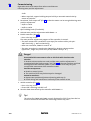
23)
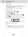
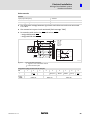
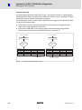
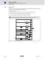
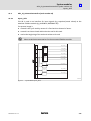
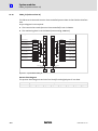
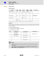
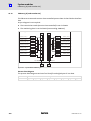
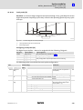
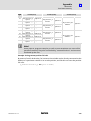
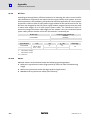
The system−block principle can be explained by means of a PLC system in a rack:
ƒ
The rack contains the CPU, digital I/Os, analog I/Os, counter card, positioning card,
etc. as additional cards:
CPU
x
x
x
x
x
x
x = Additional cards
ƒ
The CPU can directly access the additional cards and process the resulting
information.
ƒ
Additional cards have fixed addresses for access.
Tip!
In case of the ECSxA... axis modules, the system blocks correspond to these
attachment cards!
System blocks therefore are specific (hardware) function blocks which are
firmly integrated into the runtime system of the ECSxA... axis module.
18
EDBCSXA064 EN 2.0
Preface and general information
1
System block introduction
System blocks ˘ principle
1.5.2
Node numbers
The system blocks feature the following node numbers:
Node
number
System block
Notes
1
DIGITAL_IO
Digital inputs/outputs
11
ANALOG1_IO
Analog input 1
21
DFIN_IO_DigitalFrequency
Digital frequency input
22
DFOUT_IO_DigitalFrequency
31
32
33
34
35
36
41
42
43
60
CAN1_IO
CAN2_IO
CAN3_IO
CANaux1_IO
CANaux2_IO
CANaux3_IO
AIF1_IO_AutomationInterface
AIF2_IO_AutomationInterface
AIF3_IO_AutomationInterface
OSC_Oscilloscope
Digital frequency output
System bus (CAN)
101
CAN_Management
System bus (CAN) management
102
CAN_Synchronization
System bus (CAN) synchronisation
111
CANaux_Management
System bus (CAN−AUX) management
121
DCTRL_DriveControl
Device control
131
MCTRL_MotorControl
Motor control
141
FCODE_FreeCodes
Free codes
151
SYSTEM_FLAGS
System flags
161
AIF_IO_Management
Automation interface management
171
VAR_PERSISTENT
Persistent variables
System bus (CAN−AUX)
Automation interface (AIF)
Oscilloscope function
The node number is part of the absolute SB address. (
21)
EDBCSXA064 EN 2.0
19
1
Preface and general information
System block introduction
Access via system variables
1.5.3
Access via system variables
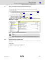
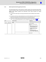
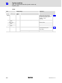
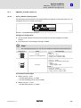
If you have integrated a system block into the system configuration of the DDS, you can use
its system variables within your project.
You can call up the input assistance in the editors of the DDS via <F2>, among other things
listing all the system variables that are provided:
In this Manual, the system variables can be retrieved in the system variable table of the
corresponding system block.
Example: Table with the inputs of the SB Inputs_Digital of the ECSxA... axis module
Variable
Address
Display
code
Display
format
DIGIN_bCInh_b
%IX1.0.0
˘
˘
DIGIN_bIn1_b
%IX1.0.1
C0443
bin
DIGIN_bIn2_b
20
Data
type
BOOL
Signal
type
binary
Notes
Controller inhibit ˘ takes
direct effect on the
device control DCTRL.
%IX1.0.2
DIGIN_bIn3_b
%IX1.0.3
DIGIN_bIn4_b
%IX1.0.4
DIGIN_b_safe_standstill_b
%IX1.0.5
"Safe torque off"
(former "safe standstill")
EDBCSXA064 EN 2.0
Preface and general information
1
System block introduction
Access via absolute addresses
1.5.4
Access via absolute addresses
You can also access the inputs and outputs of the system blocks via absolute addresses
according to standard IEC 61131−3:
For inputs:
For outputs:
%IXa.b.c
%QXa.b.c
a = node number
b = word address
c = bit address
In this Manual, the absolute addresses can be retrieved in the system variable table of the
corresponding system block.
Example: Table with the inputs of the SB Inputs_Digital of the ECSxA... axis module
Variable
Data
type
Address
Display
code
Display
format
DIGIN_bCInh_b
%IX1.0.0
˘
˘
DIGIN_bIn1_b
%IX1.0.1
C0443
bin
DIGIN_bIn2_b
1.5.5
BOOL
Signal
type
binary
Notes
Controller inhibit ˘ takes
direct effect on the
device control DCTRL.
%IX1.0.2
DIGIN_bIn3_b
%IX1.0.3
DIGIN_bIn4_b
%IX1.0.4
DIGIN_b_safe_standstill_b
%IX1.0.5
"Safe torque off"
(former "safe standstill")
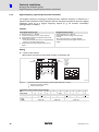
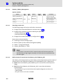
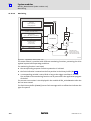
Definition of the inputs/outputs
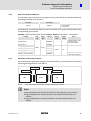
For connecting the application program with the hardware, system blocks are connected
with program organisation units (POUs):
POE-Input
POE-Output
SB-Output
SB
Fig. 1−1
SB-Input
POE
SB
Plan: Connecting system blocks to a program organisation unit (POU)
Note!
Inputs and outputs are always classified from the program’s point of view.
ƒ Logical SB inputs are always hardware−side outputs of the ECSxA axis...
module
ƒ Logical SB outputs are always hardware−side inputs of the ECSxA axis...
module
EDBCSXA064 EN 2.0
21
1
Preface and general information
System block introduction
Definition of the inputs/outputs
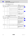
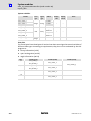
Example:
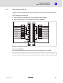
Use of the system blocks Inputs_Digital and Outputs_Digital
DIGIN_bIn1_b
DI4
1
1
DIGIN_b_safe_standstill_b
mP + Imp
DO1
X6
SO
0
DIGOUT_bRelais_b
C0444/2
DIGIN_bCInh_b
C0443
X6
1
safe torque off
POE
mP
safe standstill
0
C0118/1
DIGIN_bIn4_b
X6
SI2
C0444/1
DIGIN_bIn3_b
1
C0114/1...4
C0443
SI1
DIGOUT_bOut1_b
DIGIN_bIn2_b
0
DI2
DI3
Outputs_DIGITAL
Inputs_DIGITAL
X6
DI1
X6
1
1
X25
C0118/2
B+
B1
B-
B2
C0602
MONIT-Rel1
ECSXA207
Fig. 1−2
Plan: connecting the system blocks "Inputs_Digital" and "Outputs_Digital"
If you want to use digital input 1 and digital output 1, carry out the following steps:
1. Explicitly integrate the SBs Inputs_Digital and Outputs_Digital into the DDS control
configuration. (
23)
2. For access to digital input 1:
– Assign the system variable DIGIN_bIn1_b to a POU variable.
3. For access to digital output 1:
– Assign the system variable DIGOUT_bOut1_b to a POU variable.
Note!
According to the IEC 61131−3 standard the system variables DIGIN_bIn1_b and
DIGOUT_bOut1_b may generally only be used once.
The use of one system variable in several POUs must be carried out via a copy
(as global variable).
22
EDBCSXA064 EN 2.0
Preface and general information
1
System block introduction
Integrating system blocks into the DDS
1.5.6
Integrating system blocks into the DDS
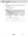
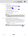
The system blocks required have to be integrated explicitly into the project in the DDS via
the control configuration.
ƒ
The control configuration is placed as an object in the Resources tab in the Object
organiser.
ƒ
The control configuration lists all inputs and outputs including the identifiers of the
corresponding system variable, the absolute address and the data type of the
system variable for every linked SB.
0
1
2
ECSXA245
Fig. 1−3
Example: Control configuration including the SBs "Inputs_DIGITAL" and "Outputs_DIGITAL"
Identifier of the system variable
Absolute address
Data type of the system variable
Tip!
The control configuration can be accessed using the right mouse key. A
context menu helps you to add and delete SBs.
EDBCSXA064 EN 2.0
23
1
Preface and general information
System block introduction
Signal types and scaling
1.5.7
Signal types and scaling
A signal type can be assigned to most inputs and outputs of the Lenze function
blocks/system blocks. The following signal types are distinguished:
ƒ
digital and analog signals
ƒ
position and speed signals
The identifier of the corresponding input/output variable has an ending (starting with an
underscore). It indicates the signal type.
Signal
Type
Symbol
Ending
Memory
Scaling
(external size º internal size)
100 % º 16384
Analog
_a (analog)
16 Bit1
Digital
_b (binary)
1 bit
0 º FALSE; 1 º TRUE
_v (velocity)
16 Bit1
15000 rpm º 16384
Angular
difference or
speed (rot.)
l
l
Angular difference/speed ref. to 1 ms
Normalisation example:
Speed (on motor side) + 15000 [rpm] + 15000
60 [s]
1 motor revolution + 65536 [inc]
ƪ ƫ
15000 @ 65536 [inc] + 16384 inc
ms
60000 [ms]
32 Bit
1 motor revolution º 65536
Variable value (..._v) +
Angle or position
_p (position)
31
High Word
Low Word
0
Direction (0 º clockwise rotation; 1 º counter−clockwise rotation)
No. of motor revolutions (0 ... 32767)
Angle or position (0 ... 65535)
Due to their scaling, analog signals have an asymmetrical resolution range
(−200 % ... +199.99 %):
24
External:
−200 %
−100 %
0%
+100 %
+199.99 %
Internal:
−32768
−16384
0
+16384
+32767
EDBCSXA064 EN 2.0
Safety instructions
2
General safety and application notes for Lenze controllers
2
Safety instructions
2.1
General safety and application notes for Lenze controllers
(in accordance with Low−Voltage Directive 2006/95/EC)
For your personal safety
Depending on their degree of protection, some parts of the Lenze controllers (frequency
inverters, servo inverters, DC speed controllers) and their accessory components can be
live, moving and rotating during operation. Surfaces can be hot.
Non−authorised removal of the required cover, inappropriate use, incorrect installation or
operation, creates the risk of severe injury to persons or damage to material assets.
For more information, please see the documentation.
High amounts of energy are produced in the controller. Therefore it is required to wear
personal protective equipment (body protection, headgear, eye protection, ear protection,
hand guard).
All operations concerning transport, installation, and commissioning as well as
maintenance must be carried out by qualified, skilled personnel (IEC 364 or
CENELEC HD 384 or DIN VDE 0100 and IEC report 664 or DIN VDE 0110 and national
regulations for the prevention of accidents must be observed).
According to this basic safety information, qualified, skilled personnel are persons who are
familiar with the assembly, installation, commissioning, and operation of the product and
who have the qualifications necessary for their occupation.
Application as directed
Controllers are components which are designed for installation in electrical systems or
machines. They are not to be used as domestic appliances, but only for industrial purposes
according to EN 61000−3−2.
When controllers are installed into machines, commissioning (i.e. starting of the operation
as directed) is prohibited until it is proven that the machine complies with the regulations
of the EC Directive 98/37/EC (Machinery Directive); EN 60204 must be observed.
Commissioning (i.e. starting of the operation as directed) is only allowed when there is
compliance with the EMC Directive (2004/108/EC).
The controllers meet the requirements of the Low−Voltage Directive 2006/95/EC. The
harmonised standard EN 61800−5−1 applies to the controllers.
The technical data and supply conditions can be obtained from the nameplate and the
documentation. They must be strictly observed.
Warning: Controllers are products which can be installed in drive systems of category C2
according to EN 61800−3. These products can cause radio interferences in residential areas.
In this case, special measures can be necessary.
Transport, storage
Please observe the notes on transport, storage, and appropriate handling.
Observe the climatic conditions according to the technical data.
EDBCSXA064 EN 2.0
25
2
Safety instructions
General safety and application notes for Lenze controllers
Installation
The controllers must be installed and cooled according to the instructions given in the
corresponding documentation.
Ensure proper handling and avoid excessive mechanical stress. Do not bend any
components and do not change any insulation distances during transport or handling. Do
not touch any electronic components and contacts.
Controllers contain electrostatic sensitive devices which can easily be damaged by
inappropriate handling. Do not damage or destroy any electrical components since this
might endanger your health!
Electrical connection
When working on live controllers, observe the applicable national regulations for the
prevention of accidents (e.g. VBG 4).
The electrical installation must be carried out according to the appropriate regulations
(e.g. cable cross−sections, fuses, PE connection). Additional information can be obtained
from the documentation.
This documentation contains information on installation in compliance with EMC
(shielding, earthing, filters, and cables). These notes must also be observed for CE−marked
controllers. The manufacturer of the system is responsible for compliance with the limit
values demanded by EMC legislation. The controllers must be installed in housings (e.g.
control cabinets) to meet the limit values for radio interferences valid at the site of
installation. The housings must enable an EMC−compliant installation. Observe in
particular that e.g. the control cabinet doors have a circumferential metal connection to
the housing. Reduce housing openings and cutouts to a minimum.
Lenze controllers can cause a direct current in the protective conductor. If a residual current
device (RCD) is used as a protective means in case of direct or indirect contact, only a
residual current device (RCD) of type B may be used on the current supply side of the
controller. Otherwise, another protective measure such as separation from the
environment through double or reinforced insulation or disconnection from the mains by
means of a transformer must be applied.
Operation
If necessary, systems including controllers must be equipped with additional monitoring
and protection devices according to the valid safety regulations (e.g. law on technical
equipment, regulations for the prevention of accidents). The controllers can be adapted to
your application. Please observe the corresponding information given in the
documentation.
After the controller has been disconnected from the supply voltage, all live components
and power connections must not be touched immediately because capacitors can still be
charged. Please observe the corresponding stickers on the controller.
All protection covers and doors must be shut during operation.
Notes for UL−approved systems with integrated controllers: UL warnings are notes that
only apply to UL systems. The documentation contains special UL notes.
Safety functions
Special controller variants support safety functions (e.g. "safe torque off", formerly "safe
standstill") according to the requirements of Appendix I No. 1.2.7 of the EC Directive
"Machinery" 98/37/EC, EN 954−1 Category 3 and EN 1037. Strictly observe the notes on
the safety functions given in the documentation for the respective variants.
26
EDBCSXA064 EN 2.0
Safety instructions
2
General safety and application notes for Lenze controllers
Maintenance and servicing
The controllers do not require any maintenance if the prescribed operating conditions are
observed.
If the ambient air is polluted, the cooling surfaces of the controller may become dirty or the
air vents may be obstructed. Therefore, clean the cooling surfaces and air vents periodically
under these operating conditions. Do not use sharp or pointed tools for this purpose!
Disposal
Recycle metal and plastic materials. Ensure professional disposal of assembled PCBs.
The product−specific safety and application notes given in these instructions must be
observed!
EDBCSXA064 EN 2.0
27
2
Safety instructions
Residual hazards
2.2
Residual hazards
Protection of persons
ƒ
Before working on the axis module, check that no voltage is applied to the power
terminals, because
– the power terminals +UG, −UG, U, V and W remain live for at least 3 minutes after
mains switch−off.
– the power terminals +UG, −UG, U, V and W remain live when the motor is stopped.
ƒ
The heatsink has an operating temperature of > 70 °C:
– Direct skin contact with the heatsink results in burns.
ƒ
The discharge current to PE is > 3.5 mA AC or. > 10 mA DC.
– EN 61800−5−1 requires a fixed installation.
– The PE connection must comply with EN 61800−5−1.
– Comply with the further requirements of EN 61800−5−1 for high discharge
currents!
Device protection
ƒ
All pluggable connection terminals must only be connected or disconnected when
no voltage is applied!
ƒ
The power terminals +UG, −UG, U, V, W and PE are not protected against polarity
reversal.
– When wiring, observe the polarity of the power terminals!
ƒ
Power must not be converted until all devices of the power system are ready for
operation. Otherwise, the input current limitation may be destroyed.
Frequent mains switching (e.g. inching mode via mains contactor) can overload and
destroy the input current limitation of the axis module, if
ƒ
the axis module is supplied via the ECSxE supply module and the input current
limitation is activated depending on the DC−bus voltage (C0175 = 1 or 2).
ƒ
the axis module is not supplied via a supply module delivered by Lenze.
ƒ
the low−voltage supply (24 V) is switched off.
For this reason allow a break of at least three minutes between two starting operations!
Use the safety function ˜Safe torque off˜ (STO) for frequent disconnections for safety
reasons.
28
EDBCSXA064 EN 2.0
Safety instructions
2
Residual hazards
Motor protection
ƒ
Only use motors with a minimum insulation resistance of û = 1.5 kV,
min. du/dt = 5 kV/ms.
– Lenze motors meet these requirements.
ƒ
When using motors with an unknown insulation resistance, please contact your
motor supplier.
ƒ
Some settings of the axis module lead to an overheating of the connected motor,
e.g. longer operation of self−ventilated motors with low speeds.
ƒ
Use PTC thermistors or thermostats with PTC characteristic for motor temperature
monitoring.
EDBCSXA064 EN 2.0
29
2
Safety instructions
Safety instructions for the installation according to UL or UR
2.3
Safety instructions for the installation according to UL or UR
Warnings!
General markings:
ƒ Use 60/75 °C or 75 °C copper wire only.
ƒ Maximum ambient temperature 55 °C, with reduced output current.
Markings provided for the supply units:
ƒ Suitable for use on a circuit capable of delivering not more than 5000 rms
symmetrical amperes, 480 V max, when protected by K5 or H Fuses
(400/480 V devices).
ƒ Alternate − Circuit breakers (either inverse−time, instantaneous trip types or
combination motor controller type E) may be used in lieu of above fuses
when it is shown that the let−through energy (i2t) and peak let−through
current (Ip) of the inverse−time current−limiting circuit breaker will be less
than that of the non−semiconductor type K5 fuses with which the drive has
been tested.
ƒ Alternate − An inverse−time circuit breaker may be used, sized upon the
input rating of the drive, multiplied by 300 %.
Markings provided for the inverter units:
ƒ The inverter units shall be used with supply units which are provided with
overvoltage devices or systems in accordance with UL840 2nd ed., Table 5.1.
ƒ The devices are provided with integral overload and integral thermal
protection for the motor.
ƒ The devices are not provided with overspeed protection.
Terminal tightening torque of lb−in (Nm)
Terminal
lb−in
Nm
X 21, X 22, X 23, X 24
10.6 ... 13.3
1.2 ... 1.5
X4, X6, X14
1.95 ... 2.2
0.22 ... 0.25
X 25
4.4 ... 7.1
0.5 ... 0.8
Wiring diagram AWG
30
Terminal
AWG
X 21, X 22, X 23, X 24
12 ... 8
X4, X6, X14
28 ... 16
X 25
24 ... 12
EDBCSXA064 EN 2.0
Safety instructions
2
Definition of notes used
2.4
Definition of notes used
The following pictographs and signal words are used in this documentation to indicate
dangers and important information:
Safety instructions
Structure of safety instructions:
Danger!
(characterises the type and severity of danger)
Note
(describes the danger and gives information about how to prevent dangerous
situations)
Pictograph and signal word
Meaning
Danger!
Danger of personal injury through dangerous electrical voltage.
Reference to an imminent danger that may result in death or
serious personal injury if the corresponding measures are not
taken.
Danger!
Danger of personal injury through a general source of danger.
Reference to an imminent danger that may result in death or
serious personal injury if the corresponding measures are not
taken.
Stop!
Danger of property damage.
Reference to a possible danger that may result in property damage
if the corresponding measures are not taken.
Application notes
Pictograph and signal word
Meaning
Note!
Important note to ensure troublefree operation
Tip!
Useful tip for simple handling
Reference to another documentation
Special safety instructions and application notes for UL and UR
Pictograph and signal word
Meaning
Warnings!
Safety or application note for the operation of a UL−approved
device in UL−approved systems.
Possibly the drive system is not operated in compliance with UL if
the corresponding measures are not taken.
Warnings!
Safety or application note for the operation of a UR−approved
device in UL−approved systems.
Possibly the drive system is not operated in compliance with UL if
the corresponding measures are not taken.
EDBCSXA064 EN 2.0
31
3
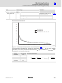
Technical data
General data and operating conditions
3
Technical data
3.1
General data and operating conditions
Standards and operating conditions
Conformity
CE
Low−Voltage Directive (73/23/EEC)
Approvals
UL 508C
Power conversion equipment
Underwriter Laboratories (File No. E132659)
for USA and Canada
50 m
For rated mains voltage and switching frequency of 8 kHz
Max. permissible
motor cable length
shielded
Packaging (DIN 4180)
Delivery packing
Installation
l
l
Mounting position
Free space
Installation in IP20 control cabinet
For the "safe torque off" function (formerly "safe standstill"): mounting in IP54
control cabinet
Vertically suspended
above
³ 65 mm
below
³ 65 mm
With ECSZS000X0B shield mounting kit: > 195 mm
to the sides
Side−by−side mounting without any clearance
Environmental conditions
Climate
3k3 in accordance with IEC/EN 60721−3−3
Condensation, splash water and ice formation
not permissible.
Storage
IEC/EN 60721−3−1
1K3 (−25 ... + 55 °C)
Transport
IEC/EN 60721−3−2
2K3 (−25 ... +70 °C)
Operation
IEC/EN 60721−3−3
3K3 (0 ... + 55 °C)
l Atmospheric pressure: 86 ... 106 kPa
l Above +40 °C: reduce the rated output
current by 2 %/°C.
Site altitude
0 ... 4000 m amsl
l Reduce rated output current by
5 %/1000 m above 1000 m amsl.
l Over 2000 m amsl: use is only permitted in
environments with overvoltage category II
Pollution
VDE 0110 part 2 pollution degree 2
Vibration resistance
Accelerational stability up to 0.7 g (Germanischer Lloyd, general conditions)
32
EDBCSXA064 EN 2.0
Technical data
3
General data and operating conditions
General electrical data
EMC
Compliance with EN 61800−3
Noise emission
Compliance with limit value class A to EN 55011
(achieved with application−typical collective filter)
Noise immunity
Requirements to EN 61800−3
Requirements
Standard
Severity
ESD 1)
EN 61000−4−2
3, i. e.
l 8 kV with air discharge
l 6 kV with contact discharge
High frequency in cables
EN 61000−4−6
10 V; 0.15 ... 80 MHz
RF interference (enclosure)
EN 61000−4−3
3, i. e. 10 V/m;
80 ... 1000 MHz
Burst
EN 61000−4−4
3/4, i. e. 2 kV/5 kHz
Surge (on mains cable)
EN 61000−4−5
3, i. e. 1.2/50 ms
l 1 kV phase−phase
l 2 kV phase PE
Insulation resistance
Overvoltage category III to VDE 0110
Discharge current to PE (to
EN 61800−5−1)
> 3.5 mA AC during operation
Enclosure
IP20 for
l standard mounting (built−in unit)
l Mounting in cold plate technique
l mounting with thermal separation (push−through technique), IP54 on the heatsink
side
Protective measure against
l
l
l
l
l
l
Protective insulation of control circuits
1)
EDBCSXA064 EN 2.0
Short circuit in power terminals
– Motor terminal has a limited protection against short circuit (after short circuit
detection, the error message must be reset.)
Short circuit in auxiliary circuits
– Digital outputs: protected against short circuit
– Bus and encoder systems: limited protection against short circuit (if necessary,
monitoring functions can be switched off, in this case, error messages must be
reset:)
Short to earth (protected against short to earth during operation, limited
protection against short to earth on mains power−up)
Overvoltage
Motor stalling
Motor overtemperature (input for KTY, I2 x t monitoring)
Protective isolation of mains
Double/reinforced insulation to EN 61800−5−1
Noise immunity in the above−mentioned severities must be guaranteed through the control cabinet. The
user must check the compliance with the severities!
33
3
Technical data
Rated data
3.2
Rated data
Rated data
Axis module
Type
Output power 400 V mains
ECSx004
ECSx008
ECSx016
1.3
2.6
5.3
Sr [kVA]
Data for operation with upstream supply module on
mains voltage
Umains [V]
400
480
400
480
400
480
DC−bus voltage
UDC [V]
DC−bus current
IDC [A]
2.5
2.0
4.9
3.9
9.8
7.8
Rated output current at 4 kHz
(leads to a heatsink temperature of 70 °C at an ambient
temperature of 20 °C)
Ir [A]
2.0
1.6
4.0
3.2
8.0
6.4
Rated output current at 8 kHz (leads to a heatsink
temperature of 70 °C at an ambient temperature of
20 °C) 1)
Ir [A]
1.4
1.1
2.7
2.2
5.3
4.2
Max. output current
(acceleration current)
15...770
Imax [A]
4.0
I0,eff 4 kHz [A]
Short−time standstill current
(holding current at 90 °C, 4 kHz) 2)
I0,eff 4 kHz [A]
2.3
4.6
9.1
Short−time standstill current
(holding current at 70 °C, 4 kHz) 2)
I0,eff 4 kHz [A]
3.0
6.0
12.0
Short−time standstill current
(holding current at 70 °C, 8 kHz) 2)
I0,eff 8 kHz [A]
1.5
3.0
6.0
13.3
17.3
20.7
14.0
29.0
64.0
Max. output frequency
Weight
Interior
Heatsink
Ploss [W]
4.0
3.2
fout [Hz]
600
m [kg]
approx. 2.4
8.0
6.4
1)
If the heatsink temperature reaches 70 °C, the switching frequency automatically changes to 4 kHz.
2)
The indicated temperature is the measured heatsink temperature (C0061).
Application software:
S = Speed & Torque
P = Posi & Shaft
M = Motion
34
1.6
16.0
Continuous current at standstill
(holding current at 90 °C, 4 kHz)
Power loss (operation with rated
current at 4 kHz / 8 kHz)
2.0
8.0
A = Application
EDBCSXA064 EN 2.0
Technical data
3
Rated data
Rated data
Axis module
Type
Output power 400 V mains
ECSx032
ECSx048
ECSx064
8.3
11.2
13.2
Sr [kVA]
Data for operation with upstream supply module on
mains voltage
Umains [V]
DC−bus voltage
UDC [V]
DC−bus current
400
480
400
480
400
480
15...770
IDC [A]
15.6
12.5
20.9
16.8
24.5
19.6
Rated output current at 4 kHz
(leads to a heatsink temperature of 70 °C at an ambient
temperature of 20 °C)
Ir [A]
12.7
10.2
17.0
13.6
20.0
16.0
Rated output current at 8 kHz (leads to a heatsink
temperature of 70 °C at an ambient temperature of
20 °C) 1)
Ir [A]
8.5
6.8
11.3
9.0
13.3
10.6
Max. output current
(acceleration current)
Imax [A]
32.0
48.0
64.0
Continuous current at standstill 2)
(holding current at 90 °C, 4 kHz)
I0,eff 4 kHz [A]
Short−time standstill current
(holding current at 90 °C, 4 kHz) 2)
I0,eff 4 kHz [A]
18.1
27.2
36.3
Short−time standstill current
(holding current at 70 °C, 4 kHz) 2)
I0,eff 4 kHz [A]
24.0
36.0
48.0
Short−time standstill current
(holding current at 70 °C, 8 kHz) 2)
I0,eff 8 kHz [A]
12.1
18.1
24.2
27.5
34.5
41.0
117.0
132.0
158.0
Power loss (operation with rated
current at 4 kHz / 8 kHz)
Max. output frequency
Weight
Interior
Heatsink
Ploss [W]
16.0
12.8
fout [Hz]
m [kg]
23.0
18.4
27.0
21.6
600
approx. 2.4
approx. 3.3
1)
If the heatsink temperature reaches 70 °C, the switching frequency automatically changes to 4 kHz.
2)
The indicated temperature is the measured heatsink temperature (C0061).
Application software:
S = Speed & Torque
P = Posi & Shaft
M = Motion
EDBCSXA064 EN 2.0
A = Application
35
3
Technical data
Current characteristics
Increased continuous current depending on the control factor
3.3
Current characteristics
3.3.1
Increased continuous current depending on the control factor
In the lower speed range ˘ the motor does not need the full motor voltage ˘ particularly
the more powerful ECS axis modules can be permanently operated with increased output
current (cp. continuous current I0,eff 34).
I [A]
30.0
I 0 [A]
27.0
ECSxS/P/M/A064
23.0
ECSxS/P/M/A048
25.0
I N [A]
20.0
20.0
17.0
16.0
ECSxS/P/M/A032
15.0
12.7
10.0
5.0
8.0
ECSxS/P/M/A016
4.0
ECSxS/P/M/A008
4.0
2.0
ECSxS/P/M/A004
2.0
8.0
0.0
0%
50 %
100 %
U Mot_n / U Mot_max
ECSXA002
Fig. 3−1
Continuous device current, depending on the output voltage for Umains £ 400 V at 4 kHz
Ir
UMot_n
UMot_max
Rated output current of the axis module
Actual controller output voltage
0.9 x current mains voltage
The permissible continuous current depends on the control factor of the power output
stages, approximately on the ratio of the motor voltage output in the operating point
(UMot_n) to the maximum possible output voltage (UMot_max). Due to voltage drops across
the components involved at rated load and a control margin, UMot_max can be estimated
with 90 % of the mains voltage.
36
EDBCSXA064 EN 2.0
Technical data
3
Current characteristics
Increased continuous current depending on the control factor
The following table shows the connections between mains voltage, DC−bus voltage and
motor voltage:
Mains voltage
[Umains]
DC−bus voltage
[UDC = Umains x 1.35]
3 x 230 V AC
310 V DC
Output voltage (motor voltage)
nominally achievable for 100 %
modulation
[Umot = 0.66 x UDC]
3 x 205 V AC
3 x 380 V AC
510 V DC
3 x 340 V AC
3 x 400 V AC
540 V DC
3 x 360 V AC
3 x 415 V AC
560 V DC
3 x 370 V AC
3 x 460 V AC
620 V DC
3 x 415 V AC
3 x 480 V AC
650 V DC
3 x 435 V AC
3 x 528 V AC
712 V DC
3 x 475 V AC
For steady−state operation in generator mode with increased DC−bus voltage or supply
from a closed−loop DC−voltage source, interpolate accordingly between the values given in
the table.
The increased rated currents are valid for the entire voltage range specified at switching
frequencies of 4 kHz and 8 kHz.
Note!
If in this connection a heatsink temperature of > 70 °C is reached, the drive
switches to a switching frequency of 4 kHz, independently of the selected
switching frequency.
Tip!
The operating threshold of the I x t monitoring is automatically derived from
the variable continuous currents.
EDBCSXA064 EN 2.0
37
3
Technical data
Current characteristics
Increased continuous current depending on the control factor
Example:
The ECS axis module suitable for operation in conjunction with a Lenze motor of type
MCS 14L32 is to be determined.
ƒ
Rated motor data
– Rated motor torque (Mmot) = 17.2 Nm
– Rated motor speed (nmot) = 3225 rpm
– Motor voltage at 3250 rpm (Umot_n3250) = 275 V
– Rated motor current (Imot) = 15 A
– Max. motor current (Imot_max) = 92 A
ƒ
Application data:
– Max. torque (Mmax) = 35 Nm
– Max. operating speed (nmax) = 2500 rpm
– An effective process power (Peff) of 4.5 kW arises on the basis of the Mn diagram.
– The drive rating results in an effective motor current (IMot_eff) of 14.8 A.
A first estimation based on the rated current of the ECS axis module would probably lead
to selecting the ECSxA048 module with a rated current of 17.0 A.
However, if we take into account the increased continuous current for smaller control
factors, the more cost−effective ECSxA032 axis module with a rated current of 12.7 A can
be used here.
ƒ
When the MCS 14L32 is operated with 2500 rpm, the real motor voltage is
(UMot_n2500):
n
U Mot_n2500 + U Mot_n3250 @ nmax
Mot
ƒ
Þ
275V @
2500rpm
+ 212V
3250rpm
This leads to the following max. control factor (αmax) of the axis module:
a max +
U Mot_n2500
U max
Þ
212V + 0.59 + 59%
360V
Using the current characteristic of Fig. 3−1 ( 36), a continuous current of 15.5 A can
be determined for the ECSxA032 axis module when the control factor (αmax) is 59 %.
ƒ
38
Result:
Under the conditions mentioned above the MCS 14L32 Lenze motor can be operated
continuously on the ECSxA032 axis module.
EDBCSXA064 EN 2.0
Technical data
3
Current characteristics
Device protection by current derating
3.3.2
Device protection by current derating
The maximum output current is limited. With output frequencies < 5 Hz the limitation
depends on the heatsink temperature.
I out
I max
1.00
0.67
1.00
£ 70 °C
0.75
90 °C
0.57
0.38
0.00
0
5
10
f out [Hz]
ECSXA024
Fig. 3−2
Current derating characteristics
Operation with switching frequency = 8 kHz (C0018 = 1).
l If the current exceeds the characteristic , the switching frequency is automatically
changed to 4 kHz (e.g. for higher torque in acceleration processes).
Operation with switching frequency = 4 kHz (C0018 = 0).
l The current limitation follows the characteristic .
l With output frequencies < 5 Hz and heatsink temperatures between 70 and 90 °C the
current limit is steplessly adjusted in the range .
Type
Imax [A]
Switching frequency 8 kHz
Switching frequency 4 kHz
fout > 5 Hz
fout 0 Hz
fout > 5 Hz
ECSxA004
2.7
1.5
4.0
ECSxA008
5.3
3.0
ECSxA016
10.7
6.0
ECSxA032
21.3
12.1
ECSxA048
32.0
ECSxA064
42.7
EDBCSXA064 EN 2.0
fout 0 Hz
£ 70 °C
3.0
fout 0 Hz
90 °C
2.3
8.0
6.0
4.6
16.0
12.0
9.1
32.0
24.0
18.1
18.1
48.0
36.3
27.2
24.2
64.0
48.0
36.3
39
4
Mechanical installation
Important notes
4
Mechanical installation
4.1
Important notes
40
ƒ
Axis modules of the ECS series provide IP20 enclosure and can therefore only be
used for installation in control cabinets.
ƒ
If the cooling air contains air pollutants (dust, fluff, grease, aggressive gases):
– Take suitable preventive measures , e.g. separate air duct, installation of filters,
regular cleaning.
ƒ
Possible mounting positions:
– Vertical at the mounting plate
– DC bus connections (X23) at the top
– Motor connection (X24) at the bottom
ƒ
Maintain the specified clearances (above and below) to other installations!
– If the ECSZS000X0B shield mounting kit is used, an additional clearance is
required.
– Ensure unimpeded ventilation of cooling air and outlet of exhaust air.
– Several modules of the ECS series can be installed in the control cabinet next to
each other without any clearance.
ƒ
The mounting plate of the control cabinet
– must be electrically conductive.
– must not be varnished.
ƒ
In case of continuous vibrations or shocks use shock absorbers.
EDBCSXA064 EN 2.0
Mechanical installation
4
Mounting with fixing rails (standard installation)
Dimensions
4.2
Mounting with fixing rails (standard installation)
4.2.1
Dimensions
Note!
Mounting with ECSZS000X0B shield mounting kit:
ƒ Mounting clearance below the module > 195 mm
0
1
h
g
³ 65 mm
b
d
d1
b
d
d1
h
³ 65 mm
g
g
g
e
a
a
ECSxA005
Fig. 4−1
Dimensions for "panel−mounted" design
Axis module
Type
Dimensions [mm]
Size
a
88.5
b
d
d1
e
h
g
240
276
260
176
212 1)
10
6.5
(M6)
ECSEA004
ECSEA008
ECSEA016
ECSEA032
ECSEA048
ECSEA064
1)
EDBCSXA064 EN 2.0
131
max. 212 mm, depending on the plugged−on communication module
41
4
Mechanical installation
Mounting with fixing rails (standard installation)
Mounting steps
4.2.2
Mounting steps
How to install the axis module:
1. Prepare the fixing holes on the mounting surface.
– Use the drilling jig for this purpose.
2. Take the fixing rails from the accessory kit in the cardboard box.
3. Push the rails into the slots of the heatsink:
– From above: Push in the long side.
– From below: Push in the short side.
4. Attach the axis module to the mounting surface.
42
EDBCSXA064 EN 2.0
Mechanical installation
4
Mounting with thermal separation (push−through technique)
4.3
Mounting with thermal separation (push−through technique)
For the push−through technique the rear panel of the control cabinet must be a steel plate
with a thickness of at least 2 mm.
The edges of the mounting cutout and the fixing holes for the clamps must be slightly
curved inwards (towards the axis module).
Cooling
With the separated heatsink the heat generation in the control cabinet can be reduced.
ƒ
Distribution of the power loss:
– approx. 65 % via separated cooler
– approx. 35 % in the inside of the axis module
ƒ
Protection class of the separated cooler: IP54
– The sealing surface at the heatsink of the axis module must rest completely
against the mounting plate.
– Use a liquid thread sealant to bond the screws of the clamps.
ƒ
For sufficient cooling of the drive system:
– Air flow behind the rear panel of the control cabinet must be ³ 3 m/s (e.g. by means
of a collective fan).
ƒ
With sufficient cooling, the rated data of the axis modules remain valid.
EDBCSXA064 EN 2.0
43
4
Mechanical installation
Mounting with thermal separation (push−through technique)
Dimensions
4.3.1
Dimensions
Note!
Mounting with ECSZS000X0B shield mounting kit:
ƒ Mounting clearance below the module > 195 mm
³ 65 mm
0
a1
1
Z
Z
a1
g
g
c1
a
e1
d
d
b
³ 65 mm
e
b
b1
b1
h
h
g
c1
a
g
ECSXA007
Fig. 4−2
Dimensions for "push−through design"
Z
Mounting cutout (a1 x b1), 45
Axis module
Type
Dimensions [mm]
Size
a
a1
88.5
78.5
b
b1
c1
d
e
e1
g
h
240
197
75
250
109
145 1)
67
M5
10.5
ECSDA004
ECSDA008
ECSDA016
ECSDA032
ECSDA048
ECSDA064
1)
44
131
121.5
max. 145 mm, depending on the plugged−on communication module
EDBCSXA064 EN 2.0
Mechanical installation
4
Mounting with thermal separation (push−through technique)
Dimensions
Dimensions of mounting cutout
Note!
a1
c1
c1
h
a1
g
³ 90 mm
b1
b1
d
g
³ 70 mm
Installation with shield mounting ECSZS000X0B:
ƒ Clearance below the mounting cutout > 220 mm
0
1
2
ECSXA063
Fig. 4−3
Dimensions of mounting cutout
Mounting surface
Mounting cutout for size Mounting cutout for size Axis module
Type
Dimensions [mm]
Size
a1
78.5
b1
c1
d
g
h
197
75
250
M5
10.5
ECSDA004
ECSDA008
ECSDA016
ECSDA032
ECSDA048
ECSDA064
EDBCSXA064 EN 2.0
121.5
45
4
Mechanical installation
Mounting with thermal separation (push−through technique)
Mounting steps
4.3.2
Mounting steps
How to mount the axis module:
1. Prepare the fixing holes for the wire clamps on the mounting area.
– For this purpose, apply a drilling jig.
2. Prepare mounting cutout.
– The edges of the mounting cutout and the fixing holes for the wire clamps have to
be slightly arched inwardly (to the axis module).
3. Brush the threads of the screws for the wire clamps with liquid thread seal.
4. Fix the wire clamps together with the functional earth conductor supplied (Fig. 4−4).
– The functional earth conductor is part of the scope of supply of the ECSDA...axis
modules.
5. Push the axis module into the mounting cutout.
6. Engage axis module in the wire clamp at the top and the bottom.
7. Connect the functional earth conductor to the axis module (Fig. 4−4).
Note!
Fixing the functional earth conductor to the ECSDA... axis module is required
for a better electromagnetic compatibility (EMC).
ECSXA081
Fig. 4−4
Functional earth conductor at the axis module ECSDA...
46
Functional earth conductor
EDBCSXA064 EN 2.0
Mechanical installation
4
Mounting in cold−plate design
4.4
Mounting in cold−plate design
The axis modules ECSC... are intended for mounting in cold−plate design (e.g. on collective
coolers).
Requirements for collective coolers
The following requirements must be met to ensure a safe operation of the axis modules:
ƒ
Good thermal contact with the cooler
– The contact surface between collective cooler and axis module must be at least as
large as the cooling plate of the axis module.
– Smooth contact surface, max. deviation 0.05 mm.
– Connect the collective cooler with all specified screwed connections to the axis
module.
ƒ
Maintain the thermal resistance Rth according to the table.
– The values apply for operating the axis modules under rated conditions.
Axis module
Power to be dissipated
Heatsink − environment
Type
ECSCA004
ECSCA008
ECSCA016
Ploss [W]
14.0
29.0
64.0
Rth [k/W]
ECSCA032
ECSCA048
ECSCA064
117.0
132.0
158.0
ƒ
EDBCSXA064 EN 2.0
0.31
0.13
0.11
Ambient conditions:
– Furthermore the rated data regarding the ambient temperature and the derating
factors at increased temperature apply to the axis modules ( 32 et seqq.).
– Temperature of the cooling plate ("Cold Plate"): max. +85 °C
47
4
Mechanical installation
Mounting in cold−plate design
Dimensions
4.4.1
Dimensions
Note!
Mounting with ECSZS000X0B shield mounting kit:
ƒ Mounting clearance below the module > 195 mm
1
0
g
a1
g
³ 65 mm
d
b
b
³ 65 mm
a
a
a1
g
g
e
c1
c1
ECSXA009
Fig. 4−5
Dimensions for "cold−plate design"
Axis module
Type
ECSCA004
ECSCA008
ECSCA016
ECSCA032
ECSCA048
ECSCA064
1)
48
Dimensions [mm]
Size
a
a1
88.5
60
131
b
c1
d
e
g
282
50
286
121
157 1)
M6
90
max. 157 mm, depending on the plugged−on communication module
EDBCSXA064 EN 2.0
Mechanical installation
4
Mounting in cold−plate design
Mounting steps
4.4.2
Mounting steps
À
Á
Â
ECSXA030
Fig. 4−6
Mounting for "cold−plate design"
Proceed as follows to mount the axis module:
1. Prepare the fixing holes on the mounting plate.
– Use a drilling jig for this purpose.
2. Clean and degrease the contact area of collective cooler and heatsink of the
axis module (e.g. with methylated spirit).
3. Screw the support onto the collective cooler.
4. Insert the axis module from above into the support and fasten the two stud
bolts with 3.5 ... 4.5 Nm .
Note!
Penetration depth of the screws into the collective cooler: approx. 15 mm!
Tip!
The heat transfer resistance is reduced if − following step 2. −
ƒ a thin layer of heat conducting paste is applied to the contact surface or
ƒ heat conducting foil is used.
EDBCSXA064 EN 2.0
49
5
Electrical installation
Electrical isolation
5
Electrical installation
5.1
Electrical isolation
The integrated electrical isolation between the power section and the control section is a
protective separation (reinforced insulation) acc. to EN 61800−5−1.
To maintain this protective separation, it must be ensured that the external 24 V supply
and all components connected to this supply also have a protective separation (SELV/PELV)
acc. to EN 61800−5−1.
24 V supply
X6/+24, GND
Safe torque off
X6/S24, S0, SI1, SI2
Dig. input/output
Functional
insulation (50 V)
X6/DI1, DI2, DI3, DI4, DO1
D bl iinsulation
Double
l ti
Analog input
X6/AI+, AI−, AG
CAN
X4, X14
DC bus
AIF
X23
X1
Analog input configuration
Motor
X3
X24
Resolver
X7
Encoder
X8
Brake connection
X25
Brake supply
X6/B+, B−
Fig. 5−1
50
Electrical isolation
EDBCSXA064 EN 2.0
Electrical installation
5
Installation according to EMC (installation of a CE−typical drive system)
5.2
Installation according to EMC (installation of a CE−typical drive system)
General information
ƒ
The electromagnetic compatibility of a machine depends on the type of installation
and care taken. Especially consider the following:
– Assembly
– Filters
– Shielding
– Earthing
ƒ
For diverging installations, the evaluation of the conformity to the EMC Directive
requires a check of the machine or system regarding the EMC limit values. This for
instance applies to:
– Use of unshielded cables
– Use of collective interference filters instead of the assigned RFI filters
– Operation without RFI filters
ƒ
The compliance of the machine application with the EMC Directive is in the
responsibility of the user.
– If you observe the following measures, you can assume that the machine will
operate without any EMC problems caused by the drive system, and that
compliance with the EMC Directive and the EMC law is achieved.
– If devices which do not comply with the CE requirements concerning noise
immunity EN 61000−6−2 are operated close to the axis modules, these devices may
be electromagnetically affected by the axis modules.
Assembly
ƒ
Connect the power supply modules, capacitor modules (optional), axis modules, RFI
filters, and mains chokes to the earthed mounting plate with a surface as large as
possible.
– Mounting plates with conductive surfaces (zinc−coated or stainless steel) allow
permanent contact.
– Painted plates are not suitable for an EMC−compliant installation.
ƒ
If you use the ECSxK... capacitor module:
– Install the capacitor module between the power supply module and the axis
module(s).
– If the total cable length in the DC−bus connection is > 5 m, install the capacitor
module as close as possible to the axis module with the greatest power.
ƒ
Use of several mounting plates:
– Connect as much surface of the mounting plates as possible (e.g. with copper
bands).
ƒ
Ensure the separation of motor cable and signal or mains cables.
ƒ
Avoid a common terminal/power strip for the mains input and motor output.
ƒ
Lay the cables as close as possible to the reference potential. Freely suspended
cables act like aerials.
EDBCSXA064 EN 2.0
51
5
Electrical installation
Installation according to EMC (installation of a CE−typical drive system)
Filters
Only use RFI filters and mains chokes which are assigned to the power supply modules:
ƒ
RFI filters reduce impermissible high−frequency interferences to a permissible value.
ƒ
Mains chokes reduce low−frequency interferences which depend on the motor
cables and their lengths.
Shielding
ƒ
Connect the motor cable shield to the axis module
– with the ECSZS000X0B shield mounting kit.
– to the mounting plate below the axis module with a large surface.
– Recommendation: For the shield connection, use ground clamps on bare metal
mounting surfaces.
ƒ
If contactors, motor−protecting switches or terminals are located in the motor cable:
– Connect the shields of the connected cables and connect the shields to the
mounting plate, too, with a surface as large as possible.
ƒ
Connect the shield in the motor terminal box or on the motor housing to PE:
– Metal glands at the motor terminal box ensure a large−surface connection of the
shield and the motor housing.
ƒ
Shield the control cables:
– Connect both shield ends of the digital control cables.
– Connect one shield end of the analog control cables.
– Always connect the shields to the shield connection at the axis module over the
shortest possible distance.
ƒ
Using the axis modules in residential areas:
– Additionally dampen the shield in order to limit the interfering radiation: ³10 dB .
This can be implemented by using standard, closed, metallic, and earthed control
cabinets or boxes.
Earthing
52
ƒ
Earth all metallically conductive components (e. g. power supply module, capacitor
module, axis module, RFI filter, motor filter, mains choke) using suitable cables
connected to a central point (PE bar).
ƒ
Maintain the minimum cross−sections prescribed in the safety regulations:
– For the EMC, not the cable cross−section is important, but the cable surface and the
contact surface which should be as large as possible.
EDBCSXA064 EN 2.0
Electrical installation
5
Power terminals
5.3
Power terminals
ECSXA080
Fig. 5−2
Plug connectors for power terminals
Danger!
Dangerous voltage
The leakage current to earth (PE) is > 3.5 mA AC or > 10 mA DC.
Possible consequences:
ƒ Death or severe injuries when the device is touched in the event of a fault.
Protective measures:
ƒ Implement the actions required in the EN 61800−5−1. Especially:
– Fixed installation
– PE connection must conform to standards (PE conductor diameter
³ 10 mm2 or PE conductor must be connected twice)
Stop!
No device protection in the event of too high mains voltages
The mains input is not fused internally.
Possible consequences:
ƒ Destruction of the device if the mains voltage is too high.
Protective measures:
ƒ Observe the max. permissible mains voltage.
ƒ Fuse the device correctly on the supply side against mains fluctuations and
voltage peaks.
EDBCSXA064 EN 2.0
53
5
Electrical installation
Power terminals
ƒ
All power connections are plug connections and coded. The ECSZA000X0B plug
connector set must be ordered separately.
ƒ
Installation of the cables to EN 60204−1.
ƒ
The cables used must comply with the approvals required at the site of use (e.g. VDE,
UL, etc.).
Note!
ECSDA... axis modules:
For a better electromagnetic compatibility (EMC), connect the functional earth
conductor to the ECSDA... axis module ( 46).
This is not required for the ECSEA... (standard installation) and ECSCA... (cold
plate) axis modules!
Assignment of the plug connectors
Plug
Function
connector/terminal
X23
X23/+UG
X23/+UG
X23/−UG
X23/−UG
X23/PE
X23/PE
54
Electrical data
DC−bus voltage connection
Positive DC−bus voltage
Dependent on application and type
0 ... 770 V
2 ... 24.5 A ( 34)
Negative DC−bus voltage
Earth connection
X24
Motor connection
X24/U
X24/V
X24/W
X24/PE
Motor phase U
Motor phase V
Motor phase W
Earth connection
X25
Motor holding brake connection
X25/BD1
X25/BD2
Brake connection +
Brake connection −
Dependent on application and type
0 ... 480 V
1.6 ... 20 A ( 34)
23 ... 30 V DC,
max. 1.5 A
EDBCSXA064 EN 2.0
Electrical installation
5
Power terminals
Cable cross−sections and screw−tightening torques
Cable type
Wire end ferrule
Possible cable
cross−sections
Tightening torque
Stripping length
Plug connectors X23 and X24
rigid
flexible
0.2 ... 10 mm2
(AWG 24 ... 8)
˘
without wire end ferrule
0.2 ... 10 mm2
(AWG 24 ... 8)
with wire end ferrule
0.25 ... 6 mm2
(AWG 22 ... 10)
with TWIN wire end ferrule
0.25 ... 4 mm2
(AWG 22 ... 12)
1.2 ... 1.5 Nm
(10.6 ... 13.3 lb−in)
5 mm
0.5 ... 0.8 Nm
(4.4 ... 7.1 lb−in)
5 mm
−−−
10 mm
Plug connector X25
flexible
screw
connection
flexible
spring
connection
with insulated wire end
ferrule
0.25 ... 2.5 mm2
(AWG 22 ... 12)
without wire end ferrule
0.2 ... 2.5 mm2
(AWG 24 ... 12)
with insulated wire end
ferrule
0.25 ... 2.5 mm2
(AWG 22 ... 12)
without wire end ferrule
0.2 ... 2.5 mm2
(AWG 24 ... 12)
Shielded cables
The following factors decisively determine the effect of the shielded cables:
ƒ
Good shield connection
– Ensure a contact surface as large as possible
ƒ
Low shield resistance
– Only use shields with tin−plated or nickel−plated copper braids (shields with steel
braids cannot be used).
ƒ
High overlap rate of the braid
– At least 70 ... 80 % with 90° overlap angle
The ECSZS000X0B shield mounting kit includes a wire clamp and shield sheet.
EDBCSXA064 EN 2.0
55
5
Electrical installation
Power terminals
Connection to the DC bus (+UG, −UG)
5.3.1
Connection to the DC bus (+UG, −UG)
Stop!
No device protection for DC bus voltage surges
In passive axis modules (without 24 V−supply), the charging circuit can be
overloaded through DC bus voltage surges.
Possible consequences:
ƒ Destruction of the device
Protective measures:
ƒ All axis modules in the DC−bus connection should be basically supplied with
a control voltage of 24 V.
ƒ
If the total cable length is > 20 m, install an axis module or a capacitor module
directly at the power supply module.
ƒ
Design the ±UG cables twisted and as short as possible. Ensure short−circuit−proof
routing!
ƒ
Cable length (module « module) > 30 cm: install shielded ±UG cables.
Cable cross−sections
Cable length 1)
Wire end ferrule
Cable cross−
section
Without wire end ferrule
Up to 20 m
6 mm2
(AWG 10)
With wire end ferrule
Without wire end ferrule
> 20 m
1)
With wire end ferrule
Use pin−end connectors for wiring!
10 mm2
(AWG 8)
Tightening torque
Stripping
length
1.2 ... 1.5 Nm
(10.6 ... 13.3 lb−in)
5 mm
Respective cable length from module to module
Fuses
ƒ
When using ECSxE power supply modules which are fused on the supply side the
DC−bus supply need not be fused.
ƒ
When ECS axis modules are supplied by devices of the 82xx or 93xx series which can
supply a continuous current > 40 A, use the following fuses between the supplying
device and the ECS devices:
Fuse
Support
Value [A]
Lenze type
Lenze type
50
EFSGR0500ANIN
EFH20007
Warnings!
ƒ Use UL−approved cables, fuses and fuse holders only.
ƒ UL fuse:
– Voltage 500 ... 600 V
– Tripping characteristic "H", "K5" or "CC"
56
EDBCSXA064 EN 2.0
Electrical installation
5
Power terminals
Connection to the DC bus (+UG, −UG)
Replacing defective fuses
Danger!
Hazardous electrical voltage
Components can carry hazardous voltages until up to 3 minutes after
power−off.
Possible consequences:
ƒ Death or severe injuries when touching the device.
Protective measures:
ƒ Replace fuses in the deenergised state only.
– Set controller inhibit (CINH) for all axis modules in DC−bus operation and
disconnect all power supply modules from the mains.
EDBCSXA064 EN 2.0
57
5
Electrical installation
Power terminals
Connection plans
5.3.2
Connection plans
Observe...
the notes in the detailed documentation of the power supply module.
Minimum wiring for internal brake resistor
The ECSEE... and ECSDE... power supply modules are provided with an integrated brake
resistor. For using the internal brake resistor, carry out the following wiring:
ƒ
Jumper between X22/BR0 and X22/+UG (internal brake resistor connected with
brake transistor)
ƒ
Jumper between X6/T1 and X6/T2 (temperature monitoring of non−installed
external brake resistor deactivated)
K1
L1
L2
L3
N
F4
F1...F3
Z1
Off
"
On
"
L1
K1
L2
L3
PE
BR0 BR1 +UG +UG -UG PE
ECSEE...
ECSDE...
K1
+UG +UG -UG -UG PE
Rb
T1
...
PE
X23
ECSxS/P/M/A...
X6
T2
+UG +UG -UG -UG PE
PE
X23
X22
X21
X25
X24
BD1 BD2
U V W PE
X7
"
"
"
"
M
3~
ECSxS/P/M/A...
J
+
0
6
R
2
X25
X24
BD1 BD2
U V W PE
X7
"
"
"
"
M
3~
+
J
0
6
R
2
ECSXA011
Fig. 5−3
Interconnected power system with internal brake resistor
HF−shield termination by large−surface connection to functional earth (see Mounting
Instructions for ECSZS000X0B shield mounting kit)
Twisted cables
K1
F1 ... F4
Z1
Rb
58
Mains contactor
Fuse
Mains choke / mains filter, optional
Brake resistor
System cable ˘ feedback
EDBCSXA064 EN 2.0
Electrical installation
5
Power terminals
Connection plans
Minimum wiring with external brake resistor
Due to its design, the ECSCE... power supply module is not equipped with an integrated
brake resistor. Therefore, install an ERBM..., ERBS... or ERBD... brake resistor:
ƒ
Connect the brake resistor to X22/BR1 and X22/+UG.
ƒ
Connect a temperature sensor (NC contact) to X6/T1 and X6/T2.
K1
L1
L2
L3
N
F4
F1...F3
Rb
Z1
J
"
Off
"
L1
L2
L3
PE
BR0 BR1 +UG +UG -UG PE
X21
On
+UG +UG -UG -UG PE
T1
J
T2
X6
K1
...
X25
X24
BD1 BD2
U V W PE
ECSxS/P/M/A...
X7
"
Rb
PE
X23
ECSxS/P/M/A...
ECSCE...
K1
+UG +UG -UG -UG PE
PE
X23
X22
0
"
"
"
M
3~
+
J
6
R
2
X25
X24
BD1 BD2
U V W PE
X7
"
0
"
"
"
M
3~
+
J
6
R
2
ECSXA012
Fig. 5−4
Interconnected power system with external brake resistor
HF−shield termination by large−surface connection to functional earth (see Mounting
Instructions for ECSZS000X0B shield mounting kit)
Twisted cables
K1
F1 ... F4
Z1
Rb
EDBCSXA064 EN 2.0
Mains contactor
Fuse
Mains choke / mains filter, optional
Brake resistor
System cable ˘ feedback
59
5
Electrical installation
Power terminals
Motor connection
5.3.3
Motor connection
ECSXA010
Fig. 5−5
Motor and motor holding brake connection
Motor cables
ƒ
Use low−capacitance motor cables. Capacitance per unit length:
– Core/core: max. 75 pF/m
– Core/shield: max. 150 pF/m
ƒ
Length: max. 50 m, shielded
ƒ
The cross−section of the motor cables are selected according to the motor standstill
current (I0) when using synchronous motors or according to the rated motor current
(IN) for asynchronous motors.
ƒ
Length of the unshielded ends: 40 ... 100 mm (depending on the cable cross−section)
ƒ
Lenze system cables meet these requirements.
ƒ
Use the ECSZS000X0B shield mounting kit for EMC−compliant wiring.
Further information ....
with regard to the EMC−compliant wiring can be found in the Mounting
Instructions of the ECSZS000X0B shield mounting kit.
60
EDBCSXA064 EN 2.0
Electrical installation
5
Power terminals
Motor holding brake connection
5.3.4
Motor holding brake connection
The motor holding brake
ƒ
is connected to X25/BD1 and X25/BD2
ƒ
and is supplied with low voltage via the terminals X6/B+ and X6/B−:
+23 ... +30 V DC, max.1.5 A
Stop!
ƒ Protect X6/B+ with an F 1.6 A fuse.
ƒ If no appropriate voltage (incorrect height, incorrect polarity) is applied to
the brake, it engages and can be overheated and damaged by the motor
that keeps rotating.
5.3.4.1
Spark suppressor
A spark suppressor is integrated into the axis module for the motor holding brake.
5.3.4.2
Brake monitoring
The connection of the motor holding brake can be monitored for voltage failure and cable
breakage if monitoring is activated under C0602.
Motor holding brake open (inactive):
The connection of the motor holding brake is monitored with regard to voltage failure and
cable breakage:
ƒ
Threshold value for cable breakage: 140 mA ±10 %
ƒ
Threshold value for voltage failure: +4 V ±10 %
Motor holding brake closed (active):
The connection of the motor holding brake is monitored with regard to cable breakage if
the threshold value of the voltage supply X6/B+ and X6/B− exceeds 4 V.
5.3.4.3
Requirements on the brake cables
ƒ
Use Lenze system cable with integrated brake cable.
– The shielding of the brake cable must be separated.
ƒ
Length: max. 50 m
ƒ
If a separately installed brake cable is required, lay it in a shielded manner.
Note!
By the current monitoring, an ohmic voltage loss of 1.5 V along the motor
cable is produced. The voltage loss can be compensated by a higher voltage at
the cable entry.
EDBCSXA064 EN 2.0
61
5
Electrical installation
Power terminals
Motor holding brake connection
The following applies to Lenze system cables:
U K[V] + U B[V] ) 0.08
ƪm V@ Aƫ @ L [m] @ I [A] ) 1.5[V]
L
B
Voltage for compensating the voltage loss at 6X/B+ and X6/B− [V]
UB
Rated operating voltage of the brake [V]
LL
Cable length [m]
IB
Brake current [A]
1.5 A
UK
B+
B-
X25
_
"
"
+
F 1.6 A
+23 ... +30 V DC
max. 1.5 A
BD2
_
BD1
+
X6
M
3~
+
ECSXA017
Fig. 5−6
Connection of the motor holding brake to X25
62
HF−shield termination by large surface connection to functional earth (see Mounting
Instructions of the ECSZS000X0B shield mounting kit)
EDBCSXA064 EN 2.0
Electrical installation
5
Power terminals
Connection of an ECSxK... capacitor module (optional)
5.3.5
Connection of an ECSxK... capacitor module (optional)
Observe...
the notes in the detailed documentation of the capacitor module.
K1
L1
L2
L3
N
F1...F3
F4
Z1
Off
"
On
"
L1
K1
L3
L2
PE
BR0 BR1 +UG +UG -UG PE
X22
X21
D24
ECSxS/P/M/A...
X25
X24
BD1 BD2
U V W PE
X7
"
"
"
"
"
"
1
6
M
0
3~
2
GND
PE
X23
X26
GND
+24V
DO1
DI2
T2
T1
DI1
+UG +UG -UG -UG PE
PE
X23
ECSxK...
ECSxE...
X6
K1
+UG +UG -UG -UG PE
+
J
R
2
+
24 V DC
ECSXX004
Fig. 5−7
Wiring of capacitor module ECSxK...
HF−shield termination by large−surface connection to functional earth (see Mounting
Instructions for ECSZS000X0B shield mounting kit)
Twisted cables
K1
F1 ... F4
Z1
EDBCSXA064 EN 2.0
Mains contactor
Fuse
Mains choke / mains filter, optional
Contactor relay
System cable ˘ feedback
Terminal X6/SI1 of the connected axis modules (controller enable/inhibit)
63
5
Electrical installation
Control terminals
5.4
Control terminals
ECSXA070
Fig. 5−8
Plug connectors for control terminals (X6)
For the supply of the control electronics an external 24 V DC voltage at terminals X6/+24
and X6/GND is required.
Stop!
ƒ The control cables must always be shielded to prevent interference
injections.
ƒ The voltage difference between X6/AG, X6/GND and PE of the axis module
may maximally amount to 50 V.
ƒ The voltage difference can be limited by:
– overvoltage−limiting components or
– direct connection of X6/AG and X6/GND to PE.
ƒ The wiring has to ensure that for X6/DO1 = 0 (LOW level) the connected axis
modules do not draw energy from the DC bus. Otherwise, the power supply
module may be damaged.
Shield connection of control cables and signal cables
The plate on the front of the device serves as the mounting place (two threaded holes M4)
for the shield connection of the signal cables. The screws used may extend into the inside
of the device by up to 10 mm. For optimum contact of the shield connection, use the wire
clamps from the ECSZS000X0B shield mounting kit.
64
EDBCSXA064 EN 2.0
Electrical installation
5
Control terminals
PE
BR0 BR1 +UG +UG -UG PE
X21
+UG +UG -UG -UG PE
PE
X23
X22
ECSxE...
ECSxS/P/M/A...
"
"
"
"
"
1
GND
B-
SI1
B+
U
"
2
3
+24 VDC
=
+
0
=
+
F 1,6 A
"
SI2
SO
S24
GND
AI-
AI+
DI3
DI4
DI1
DI2
DO1
GND
+24V
X6
D24
DO1
DI2
DI1
T2
T1
X6
AG
L3
L2
+24V
L1
24 VDC
4
ECSXA013
Fig. 5−9
Interconnection: Control signals with internal brake resistor
/
HF−shield termination by large−surface connection to functional earth (see Mounting
Instructions for ECSZS000X0B shield mounting kit)
Contactor relay
Voltage supply for motor holding brake 23 ... 30 V DC, max. 1.5 A
Safe torque off (formerly "safe standstill")
Controller enable/inhibit
Switch−on sequence of the auxiliary relay
The auxiliary relay (see Fig. 5−9) must only switch digital input X6/DI2 of the power
supply module.
The switch−on sequence is as follows:
1. The higher−level control system or the operator switches digital input X6/DI1 of the
power supply module to HIGH.
– The DC bus is charged.
2. Digital output X6/DO1 of the axis module switches digital input X6/DI2 of the
power supply module via relay .
– In the ECS axis modules, X6/DO1 is set to "Ready" in the Lenze setting. "Ready" is
only set when the minimum DC−bus voltage is reached.
3. If X6/DI1 = HIGH and X6/DI2 = HIGH at the power supply module, X6/DO1 is
switched.
– X6/DO1 of the power supply module switches the controller enable of the axis
modules.
The above switch−on sequence must be observed to ensure that the axes will only be
enabled after the DC bus has been charged. Otherwise, the switch−on circuit in the power
supply module can be overloaded.
EDBCSXA064 EN 2.0
65
5
Electrical installation
Control terminals
Assignment of the plug connectors
Plug connector X6
Terminal
Function
Electrical data
X6/+24
Low−voltage supply of the control electronics
X6/GND
Reference potential of low−voltage supply
20 ... 30 V DC, 0. A (max. 1 A)
for starting current of 24 V:
max. 2 A for 50 ms
X6/DO1
Digital output 1
24 V DC, 0.7 A (max. 1.4 A)
short−circuit−proof
X6/DI1
Digital input 1
X6/DI2
Digital input 2
X6/DI3
Digital input 3
X6/DI4
Digital input 4
LOW:
−3 ... +5 V;
−3 ... +1.5 mA
HIGH:
+15 ... +30 V;
+2 ... +15 mA
Input current at 24 V DC:
8 mA per input
X6/AI+
Analog input +
X6/AI−
Analog input −
X6/AG
Reference potential of analog input (internal
ground)
X6/B+
Brake supply +
X6/B−
Brake supply −
X6/S24
Connection of "safe torque off" (formerly "safe
standstill")
X6/SO
Adjustable with jumper strip X3:
−10 ... +10 V, max. 2 mA
−20 ... +20 mA
Resolution: 11 bits + sign
23 ... 30 V DC
max. 1.5 A
Set brake voltage so that the permissible
voltage at the brake is not under−run or
exceeded ˘ otherwise malfunction or
destruction!
69
X6/SI1
X6/SI2
Cable cross−sections and screw−tightening torques
Cable type
Wire end ferrule
Without wire end ferrule
flexible
With insulated wire end
ferrule
Cable cross−section
Tightening torque
Stripping length
0.08 ... 1.5 mm2
(AWG 28 ... 16)
0.25 ... 0.5 mm2
(AWG 22 ... 20)
0.22 ... 0.25 Nm
(1.95 ... 2.2 lb−in)
5 mm
We recommend to use control cables with a cable cross−section of 0.25 mm2.
66
EDBCSXA064 EN 2.0
Electrical installation
5
Control terminals
Digital inputs and outputs
5.4.1
Digital inputs and outputs
Stop!
If an inductive load is connected to X6/DO1, a spark suppressor with a limiting
function to max. 50 V ± 0 % must be provided.
GNDext
47k
X6
1.5 A
3k3
3k3
3k3
3k3
1k
DI1 DI2 DI3 DI4
GND
DO1
+24
"
"
_
+
24 VDC =
ECSXA014
Fig. 5−10
Digital inputs and outputs at X6
ƒ
The digital inputs X6/DI1 ... DI4 are freely assignable.
ƒ
The polarity of the digital inputs X6/DI1 ... DI4 is set under C0114/x.
ƒ
The polarity of the digital output (X6/DO1) is set under C0118/1.
EDBCSXA064 EN 2.0
67
5
Electrical installation
Control terminals
Analog input
Analog input
82k5
82k5
5.4.2
X3
5
6
250R
GND
3.3 nF
3.3 nF
AI-
=
=
X6
AG
AI+
"
"
ECSXA015
Fig. 5−11
Analog input at X6
HF−shield termination by large−surface connection to functional earth (see Mounting
Instructions for ECSZS000X0B shield mounting kit)
Analog input configuration
ƒ
Set via C0034 whether the input is to be used for a master voltage or a master
current.
ƒ
Set jumper bar X3 according to setting in C0034:
Stop!
Do not plug the jumper on 3−4! The axis module cannot be initialised like this.
Jumper bar X3
5
3
1
5
3
1
68
6
4
2
6
4
2
Setting
5−6 open
Jumper on 1−2: Parking position
5−6 closed
Measuring range
C0034 = 0
l Level: −10 ... +10 V
l Resolution: 5 mV (11 Bit + sign)
l Scaling: ±10 V º±16384 º±100%
C0034 = 1
l Level: +4 ... +20 mA
l Resolution: 20 mA (10 bits without sign)
l Scaling:
+4 mA º 0 º 0 %
+20 mA º 16384 º 100 %
C0034 = 2
l Level: −20 ... +20 mA
l Resolution: 20 mA (10 bits + sign)
l Scaling: ±20 mA º±16384 º±100%
EDBCSXA064 EN 2.0
Electrical installation
5
Control terminals
Safe torque off
5.4.3
Safe torque off
The axis modules support the safety function "safe torque off" (formerly "safe standstill"),
"protection against unexpected start−up", according to the requirements of control
category 3 of EN ISO 13849. For this purpose, the axis modules are equipped with two
independent safety routes. Control category 3 is reached when the output signal at X6/SO
is checked as well.
EDBCSXA064 EN 2.0
69
5
Electrical installation
Control terminals
Safe torque off
5.4.3.1
Important notes
Installation/commissioning
ƒ
The "safe torque off" function must only be installed and commissioned by qualified
personnel.
ƒ
All control components (switches, relays, PLC, ...) and the control cabinet must meet
the requirements of EN ISO 13849. These include for instance:
– Switches, relays in enclosure IP54.
– Control cabinet in enclosure IP54.
– All other requirements can be found in EN ISO 13849.
ƒ
Wiring with insulated wire end ferrules is essential.
ƒ
All safety−relevant cables (e.g. control cable for the safety relay, feedback contact)
outside the control cabinet must be protected, e.g. in the cable duct. It must be
ensured that short circuits between the individual cables cannot occur. For further
measures, see EN ISO 13849.
ƒ
If force effects from outside (e.g. sagging of hanging loads) are to be expected when
the "safe torque off" function is active, additional measures have to be taken (e.g.
mechanical brakes).
Danger!
When using the "safe torque off" function, additional measures are required
for "emergency stops"!
There is neither an electrical isolation between motor and axis module not a
"service" or "repair switch".
Possible consequences:
ƒ Death or severe injuries
ƒ The machine/drive may be destroyed or damaged
Protective measures:
ƒ An "emergency stop" requires the electrical isolation of the motor cable, e.g.
by means of a central mains contactor with emergency stop wiring.
During operation
70
ƒ
After installation, the operator must check the "safe torque off" function.
ƒ
The function check must be repeated at regular intervals, but no later than after one
year.
EDBCSXA064 EN 2.0
Electrical installation
5
Control terminals
Safe torque off
5.4.3.2
Implementation
In the axis module, the "safe torque off" connection is implemented with optocouplers.
The optocouplers isolate the following areas electrically from each other:
ƒ
The digital inputs and outputs:
– input X6/SI1 (controller enable/inhibit)
– input X6/SI2 (pulse enable/inhibit)
– brake output X6/B+, B−
– output X6/SO ("safe torque off" active/inactive)
ƒ
The circuit for the internal control
ƒ
The final power stage
U
&
V
&
W
&
X6
Sl1
Sl2
S24
µP
>1
U
V
X
&
Y
&
Z
&
SO
GND
B+
X2
W
B-
X25
BD2
BD1
ECSXA100
Fig. 5−12
Implementation of the "safe torque off" function
Area 1:
Area 2:
Area 3:
Inputs and outputs
Circuit for the internal control
Power output stage
Stop!
Use insulated wire end ferrules when wiring the "safe torque off" circuits to
X6.
EDBCSXA064 EN 2.0
71
5
Electrical installation
Control terminals
Safe torque off
5.4.3.3
Functional description
The "safe torque off" state can be initiated any time via the input terminals X6/SI1
(controller enable/inhibit) and X6/SI2 (pulse enable/inhibit). For this purpose a LOW level
has to be applied at both terminals:
ƒ
X6/SI1 = LOW (controller inhibited):
The inverter is inhibited via the microcontroller system.
ƒ
X6/SI2 = LOW (pulses inhibited):
The supply voltage for the optocouplers of the power section driver is switched off, i.
e. the inverter can no longer be enabled and controlled via the microcontroller system.
The input signal at X6/SI2 to the hardware is additionally directed to the
microcontroller system and is evaluated for the state control there. For the external
further processing a HIGH level is output for the state "safe torque off active" at the
digital output X6/SO.
The control of the inverter thus is prevented by two different methods that are
independent of each other. Therefore an unexpected start−up by the motor is avoided.
5.4.3.4
Technical data
Terminal assignment
Plug connector X6
Terminal Function
X6/S24
Low−voltage supply
X6/SO
"Safe torque off" feedback
output
X6/SI1
X6/SI2
Level
Electrical data
18 ... 30 V DC
0.7 A
LOW
During operation
HIGH
"Safe torque off" active
Input 1 (controller
enable/inhibit)
LOW
Controller inhibited
Input 2 (pulse enable/inhibit)
LOW
HIGH
HIGH
24 V DC
0.7 A (max. 1.4 A)
Short−circuit−proof
LOW level:
−3 ... +5 V
Controller enabled
−3 ... +1.5 mA
Pulses for power section are HIGH level:
+15 ... +30 V
inhibited
+2 ... +15 mA
Pulses for power section are Input current at 24 V DC:
enabled
8 mA per input
Cable cross−sections and screw−tightening torques
Cable type
flexible
screw
connection
flexible
spring
connection
72
Wire end ferrule
with insulated wire end
ferrule
Cable cross−section
Tightening torque
Stripping length
0.22 ... 0.25 Nm
(1.95 ... 2.2 lb−in)
5 mm
−−−
9 mm
0.25 ... 1.5 mm2
(AWG 22 ... 16)
without wire end ferrule
0.14 ... 1.5 mm2
(AWG 28 ... 16)
with insulated wire end
ferrule
0.25 ... 1.5 mm2
(AWG 22 ... 16)
without wire end ferrule
0.14 ... 1.5 mm2
(AWG 28 ... 16)
EDBCSXA064 EN 2.0
Electrical installation
5
Control terminals
Safe torque off
5.4.3.5
Minimum wiring
In order to reach control category 3, the signal at X6/SO must be verified additionally. This
requires external wiring. The external wiring must be adapted to the existing safety
concepts and checked for correct operation.
Tip!
Please see page 77 for a wiring example with an electronic safety control
unit for category 3.
"Safe torque off" with multiple−contact switches
The example circuit shows the minimum external wiring of the axis module with
multiple−contact switches for a motor with brake.
24VDC
11
13
23
12
14
24
11
13
23
12
14
24
S1
S2
X6
Sl1
Sl2
S24
SO
GND
B+
B-
X25
H1
Y1
BD2
BD1
GND
ECSXA101
Fig. 5−13
Minimum external wiring with multiple−contact switches
Stop!
Observe the reaction of the drive when you activate controller enable and/or
pulse enable (X6/SI1 or SI2 = HIGH level):
ƒ The motor brake is applied immediately. This can lead to high wear on the
motor holding brake (see data sheet for the brake).
ƒ If the brake monitoring is active (C0602 = 0), TRIP "Rel1" is set. Before
recommissioning, the TRIP must be reset.
EDBCSXA064 EN 2.0
73
5
Electrical installation
Control terminals
Safe torque off
Preconditions for external wiring with multiple−contact switches:
74
ƒ
Switches S1 and S2 must have at least three contacts:
– At least one NC contact and two NO contacts. All contacts must be electrically
independent and positively driven.
– The contacts must not be bridged.
ƒ
Switches S1 and S2 must be separated mechanically to avoid simultaneous
switching after activation.
ƒ
The NO contacts of S1 and S2 must only close when the NC contacts are open. NO
and NC contacts must not be activated at the same time.
ƒ
S1 and S2 must be designed for 24 V DC voltage. If a higher voltage occurs in the
electrical environment, the switches must have an insulation voltage. The insulation
voltage must at least be as high as the highest voltage that can occur in case of an
error.
ƒ
Ensure that two channels are available for control category 3:
– Every time the controller is switched off (even in case of a single−channel
switch−off) via the contacts 13/14 of switches S1 and S2, the brake supply is
interrupted and the brake is applied. In addition, the internal brake relay must be
switched off by the application.
– The voltage supply for the output (X6/S24) via the NC contacts 11/12 of switches
S1 and S2 is only switched through in case of a two−channel controller switch−off.
This ensures that the output X6/SO will not be at HIGH level if a short−circuit
occurs in the internal transistor while the drive is not switched off via both
channels.
ƒ
The switching contacts must resist the maximum current of the 24 V DC voltage
supply.
ƒ
All control components (switches, relays, PLC, ...) and the control cabinet must meet
the requirements of EN ISO 13849. These include for instance:
– Switches, relays in enclosure IP54.
– Control cabinet in enclosure IP54.
– All other requirements can be found in EN ISO 13849.
ƒ
Wiring with wire end ferrules is essential.
ƒ
All safety−relevant cables (e.g. control cable for the safety relay, feedback contact)
outside the control cabinet must be protected, e.g. in the cable duct. It must be
ensured that short circuits between the individual cables cannot occur! For further
measures, see EN ISO 13849.
EDBCSXA064 EN 2.0
Electrical installation
5
Control terminals
Safe torque off
"Safe torque off" with safety PLC
The version "safe torque off" with safety PLC must ensure the function of the
multiple−contact switches. The following conditions must be met:
ƒ
The NO contacts only close when the NC contacts are open.
ƒ
The voltage supply for the brake must be switched off safely in the event of LOW
level at X6/SI1 and/or LOW level at X6/SI2.
ƒ
The voltage supply for the output X6/SO must be switched off safely in the event of
HIGH level at X6/SI1 and/or HIGH level at X6/SI2.
ƒ
Safe processing of the output signal at X6/SO for higher level safety concepts.
ƒ
The PLC must be programmed such that
– the input and output states of the output X6/SO are checked for plausibility
according to the following truth table.
– the entire system will immediately change to a safe state when the plausibility
check results in an impermissible state.
States of the "safe torque off" function at the axis module
Resulting level at
output terminal
Impermissible level at
output terminal
X6/SI2
X6/SO
X6/SO
LOW
LOW
HIGH
LOW
LOW
HIGH
LOW
HIGH
LOW
LOW
HIGH
HIGH
LOW
Level at input terminal
X6/SI1
HIGH
ƒ
All control components (switches, relays, PLC, ...) and the control cabinet must meet
the requirements of EN ISO 13849. These include for instance:
– Switches, relays in enclosure IP54.
– Control cabinet in enclosure IP54.
– All other requirements can be found in EN ISO 13849.
ƒ
Wiring with wire end ferrules is essential.
ƒ
All safety−relevant cables (e.g. control cable for the safety relay, feedback contact)
outside the control cabinet must be protected, e.g. in the cable duct. It must be
ensured that short circuits between the individual cables cannot occur! For further
measures, see EN ISO 13849.
EDBCSXA064 EN 2.0
75
5
Electrical installation
Control terminals
Safe torque off
5.4.3.6
Function check
ƒ
After installation the operator must check the "safe torque off" function.
ƒ
The function check must be repeated at regular intervals, after one year at the
latest.
Stop!
If the function check leads to impermissible states at the terminals,
commissioning cannot take place!
Test specifications
ƒ
Check the circuitry with regard to correct function.
ƒ
Check directly at the terminals whether the "safe torque off" function operates
faultlessly in the axis module:
States of the "safe torque off" function on the axis module
Resulting level at
output terminal
Impermissible level at
output terminal
X6/SI2
X6/SO
X6/SO
LOW
LOW
HIGH
LOW
LOW
HIGH
LOW
HIGH
LOW
LOW
HIGH
HIGH
LOW
Level at input terminal
X6/SI1
76
HIGH
EDBCSXA064 EN 2.0
Electrical installation
5
Control terminals
Safe torque off
5.4.3.7
Example: Wiring with electronic safety control unit for category 3
ECSXA102
Fig. 5−14
Example: Wiring with "Siemens 3TK2842"safety control unit
T1 Test key 1
T2 Test key 2
ƒ
The motor is shutdown in accordance with stop category 1 of EN 60204 when the
safety function is requested.
ƒ
The delay time of the safety control unit and the quick stop deceleration time have
to be coordinated with the brake closing time.
ƒ
The diode−capacitor combination prevents the test pulses of the safety control unit
from disturbing the smooth running of the motor, as otherwise a short−time inhibit
of the controller cannot be ruled out. It can be procured from the company Pilz (Pilz
order number: 774195) as a complete terminal.
Manual test of the disconnecting paths
ƒ
The disconnecting paths have to be checked individually in succession.
ƒ
If the test keys (T1, T2) are pressed, the motor has to be torqueless immediately and
the brake has to engage.
ƒ
When the safety control unit is switched off, or if both test keys are pressed at the
same time, the feedback "STO" has to signalise. This feedback is not reliable and
only serves as an information for the operator that a switch−on is possible now.
ƒ
If the actual state deviates from the facts described here, switch off the drive
immediately. Eliminate the fault before the restart is carried out.
EDBCSXA064 EN 2.0
77
5
Electrical installation
Automation interface (AIF)
5.5
Automation interface (AIF)
The keypad XT or a communication module can be attached to or removed from the
automation interface (X1). This is also possible during operation.
ƒ
The keypad XT serves to enter and visualise parameters and codes.
ƒ
The communication modules serve to network the power supply modules and axis
modules of the ECS servo system with the host system (PLC or PC).
The following combinations are possible:
Operating/communication module
Type/order number
ECSxE
ECSxS/P/M/A
Keypad XT
EMZ9371BC
ü
ü
Diagnosis terminal (keypad XT with hand−held)
E82ZBBXC
ü
ü
LECOM−A (RS232)
EMF2102IB−V004
ü
ü
LECOM−B (RS485)
EMF2102IB−V002
ü
ü
LECOM−A/B (RS232/485)
EMF2102IB−V001
ü
ü
LECOM−LI (optical fibre)
EMF2102IB−V003
ü
ü
LON
EMF2141IB
˘
ü
INTERBUS
EMF2113IB
˘
ü
PROFIBUS−DP
EMF2133IB
˘
ü
CANopen/DeviceNet
EMF2175IB
˘
ü
Can be used together with
Further information ....
on wiring and application of communication modules can be found in the
corresponding Mounting Instructions and Communication Manuals.
78
EDBCSXA064 EN 2.0
Electrical installation
5
Wiring of the system bus (CAN)
5.6
Wiring of the system bus (CAN)
Note!
System bus (CAN)
In case of the ECSxA... axis module the communication can take place with a
master system or further controllers via both CAN bus interfaces (X4 or X14).
MotionBus (CAN)
The term "MotionBus (CAN)" expresses the functionality of the CAN bus
interface X4 for the ECSxS/P/M... axis modules. In these devices the
communication with a master system or further controllers is exclusively
carried out via X4. The parameter setting and the diagnostics is exclusively
executed via the interface X14.
EDBCSXA064 EN 2.0
79
5
Electrical installation
Wiring of the system bus (CAN)
Basic wiring of the CAN buses
The two following schematic diagrams show drive systems with different master value
concepts:
ƒ
In Fig. 5−15 a higher−level control takes over the function of the master, e. g. ETC.
ƒ
In Fig. 5−16 the function of the master is enabled by a controller that is assigned to
the master.
In both representations the master value transmission is effected via the
MotionBus(CAN).
The system bus (CAN) serves to diagnose and/or parameterise the drives.
PC
M
HMI
MB
SB
X4
X14
X4
S
X14 X4
S
X14
S
ECS_COB006
Fig. 5−15
MotionBus (CAN) with higher−level control
MB
SB
M
E
PC
HMI
MotionBus (CAN), connection to plug connector X4
System bus (CAN), connection to plug connector X14
Master
Slave
PC
HMI / operating unit
PC
HMI
MB
SB
X4
X14
M
X4
X14 X4
S
X14
S
ECS_COB007
Fig. 5−16
MotionBus (CAN) with controller as master
MB
SB
M
E
PC
HMI
80
MotionBus (CAN), connection to plug connector X4
System bus (CAN), connection to plug connector X14
Master
Slave
PC
HMI / operating unit
EDBCSXA064 EN 2.0
Electrical installation
5
Wiring of the system bus (CAN)
ECS_COB003
Fig. 5−17
Bus connections on the controller
Assignment of the plug connectors
X4 (CAN)
X14 (CAN−AUX)
Description
CH
CAH
CAN−HIGH
CL
CAL
CAN−LOW
CG
CAG
Reference potential
Specification of the transmission cable
For the use of the transmission cable, follow our recommendations:
Specification of the transmission cable
Total length
£ 300 m
£ 1000 m
Cable type
LIYCY 2 x 2 x 0.5 mm2
(paired with shielding)
CYPIMF 2 x 2 x 0.5 mm2
(paired with shielding)
Cable resistance
£ 80 W/km
£ 80 W/km
Capacitance per unit
length
£ 130 nF/km
£ 60 nF/km
EDBCSXA064 EN 2.0
81
5
Electrical installation
Wiring of the system bus (CAN)
System bus(CAN) wiring
ECS_COB004
Fig. 5−18
Example: System bus (CAN) wiring via interface X4
ECS
M
82
ECS axis module
Master control, e.g. ETC
Note!
Connect one bus terminating resistor (120 W) each to the first and last node of
the system bus (CAN).
EDBCSXA064 EN 2.0
Electrical installation
5
Wiring of the system bus (CAN)
Bus cable length
Note!
Be absolutely sure to observe the permissible cable lengths.
1. Check the compliance with the total cable length in Tab. 5−1.
The total cable length is defined by the baud rate.
Baud rate [kBit/s]
Max. bus length [m]
50
1500
125
630
250
290
500
120
1000
25
Tab. 5−1 Total cable length
2. Check the compliance with the segment cable length in Tab. 5−2.
The segment cable length is defined by the cable cross−section used and by the number of nodes. Without
using a repeater, the segment cable length equals the total cable length.
Nodes
Cable cross−section
0.25 mm2
0.5 mm2
0.75 mm2
1.0 mm2
2
240 m
430 m
650 m
940 m
5
230 m
420 m
640 m
920 m
10
230 m
410 m
620 m
900 m
20
210 m
390 m
580 m
850 m
32
200 m
360 m
550 m
800 m
63
170 m
310 m
470 m
690 m
Tab. 5−2 Segment cable length
3. Compare the two values to each other.
If the value determined from Tab. 5−2 is smaller than the total cable length from Tab. 5−1 that is to be realised,
the use of repeaters is required. Repeaters divide the total cable length into segments.
Example: Selection help
Specifications
0.5 mm2 (according to cable specifications 81)
l
Cable cross−section:
l
Number of nodes:
63
l
Repeater:
Lenze−repeater, type 2176 (cable reduction: 30 m)
For the max. number of nodes (63), the following cable lengths / number of repeaters from
the specifications must be observed:
Baud rate [kbit/s]
Max. cable length [m]
Segment cable length [m]
Number of repeaters
EDBCSXA064 EN 2.0
50
1500
310
5
120
630
310
2
250
290
290
−
500
120
120
−
1000
25
25
−
83
5
Electrical installation
Wiring of the system bus (CAN)
Check repeater application
Specifications
l
Baud rate:
125 kbit/s
l
Cable cross−section:
0.5 mm2
l
Number of nodes:
28
l
Cable length:
450 m
Test steps
Cable length
See
1. Total cable length at 125 kbit/s:
630 m
Tab. 5−1
2. Segment cable length for 28 nodes and a cable cross−section of
0.5 mm2:
360 m
Tab. 5−2
3. Comparison: The value in point 2 is smaller than the cable length of 450 m to be implemented.
Conclusion
l
l
Without the use of repeaters, the cable length of 450 m that is to be implemented is not possible.
After 360 m (point 2), a repeater has to be used.
Result
l
The Lenze repeater, type 2176 (cable reduction: 30 m) is used
l
Calculation of the max. cable length:
First segment: 360
Second segment: 360 m (according to Tab. 5−1) minus 30 m (cable reduction if a repeater is used)
à Max. cable length to be implemented with a repeater: 690 m.
à Therefore, the specified cable length can be implemented.
Note!
The use of further repeaters is recommended as
ƒ a service interface
Advantage: Trouble−free connection during bus operation is possible.
ƒ Calibration interface
Advantage: The calibration/programming unit remains electrically isolated.
84
EDBCSXA064 EN 2.0
Electrical installation
5
Wiring of the feedback system
5.7
Wiring of the feedback system
Different feedback systems can be connected to the axis module:
ƒ
Resolver to X7 ( 86)
ƒ
Encoder to X8 ( 87)
– Incremental encoder with TTL level
– Sin/cos encoder with rated voltage (5 ... 8 V)
– Sin/cos absolute value encoder (single−turn/multi−turn) with serial
communication (Hiperface® interface)
Note!
If a "safe isolation" acc. to EN 61140 between the encoder cable and motor
cable (e.g. by using separating webs or separated draglines) is not ensured on
the entire cable length cable due to an installation on the system side, the
encoder cable must be provided with an insulation resistance of 300 V. Lenze
encoder cables meet this requirement.
ƒ We recommend to use Lenze encoder cables for wiring.
ƒ In case of self−prepared cables
– only use cables with shielded cores twisted in pairs.
– observe the notes on wiring/preparation on the following pages.
EDBCSXA064 EN 2.0
85
5
Electrical installation
Wiring of the feedback system
Resolver connection
5.7.1
Resolver connection
Note!
Before using a resolver from another manufacturer, please consult Lenze.
Connect a resolver via the 9−pole Sub−D socket X7.
Features
ƒ
Resolver: U = 10 V, f = 4 kHz
ƒ
Resolver and resolver supply cable are monitored for open circuit (fault
message "Sd2").
X7
Æ
mm
+REF
1
-REF
2
2
0.5
AWG
20
X7
1
3
+COS
4
-COS
5
+SIN
6
-SIN
7
R1 (+KTY)
5
0.14
6
9
26
8
R2 (-KTY)
9
KTY
ECSXA022
Fig. 5−19
Resolver connection
Assignment of socket connector X7: Sub−D 9−pole
Pin
Signal
1
2
3
4
5
6
7
8
9
+Ref
−Ref
GND
+COS
−COS
+SIN
−SIN
R1
(+KTY)
R2
(−KTY)
0.5 mm2
(AWG 20)
86
0.14 mm2
(AWG 26)
˘
EDBCSXA064 EN 2.0
Electrical installation
5
Wiring of the feedback system
Encoder connection
5.7.2
Encoder connection
Danger!
For operating systems up to and including version 7.0:
Uncontrolled movements of the drive possible when absolute value encoders
are used!
If an absolute value encoder is disconnected from the axis module during
operation, a OH3−TRIP (fault no. "0053") occurs. If the absolute value encoder
now is connected to X8 again and a TRIP−RESET is carried out, the drive may
start up in an uncontrolled manner with a high speed and a high torque. An
SD8−TRIP (fault no. "0088") will not occur, as would be expected.
Possible consequences:
ƒ Death or severest injuries
ƒ Destruction or damage of the machine/drive
Protective measures:
ƒ If a TRIP occurs during commissioning when an absolute value encoder is
used, check the history buffer C0168. If an SD8−TRIP (fault no. "0088") is at
the second or third place, it is absolutely necessary to switch off and on
again the supply of the control electronics (24 V supply).
Via the 9−pole Sub−D−plug X8, you can connect the following encoders:
ƒ
Incremental encoder
– with two 5 V complementary signals (TTL encoders) that are electrically shifted by
90°.
– Optionally, the zero track can be connected.
ƒ
Sin/cos encoder
– with rated voltage (5 ... 8 V).
– with serial communication (single−turn or multi−turn; the initialisation time of the
axis module is extended to approx. 2 s).
The controller supplies the encoder with voltage.
Use C0421 to set the supply voltage VCC (5 ... 8 V) to compensate, if required, the voltage
loss [DU] on the encoder cable:
DU ^ 2 @ L L[m] @ Rńm[Wńm] @ I G[A]
DU
Voltage loss on the encoder cable [V]
LL
Cable length [m]
R/m
Resistance per meter of cable length [W/m]
IG
Encoder current [A]
Stop!
Observe the permissible connection voltage of the encoder used. If the values
in C0421 are set too high, the encoder can be destroyed!
EDBCSXA064 EN 2.0
87
5
Electrical installation
Wiring of the feedback system
Encoder connection
Incremental encoder (TTL encoder)
Features
Input/output frequency:
0 ... 200 kHz
Current consumption:
6 mA per channel
Current on output VCC (X8/pin 4):
Max. 200 mA
< 50 m
5
B
B
1
2
3
4
5
6
7
8
9
A
A
VCC
GND
Z
Z
KTY
9
X8
R1 (+KTY)
R2 (-KTY)
6
1
A
A
B
B
Z
Z
ECSXA026
Fig. 5−20
Connection of incremental encoder with TTL level
Signals in case of clockwise rotation
Cores twisted in pairs
Assignment of plug connector X8: Sub−D 9−pole
Pin
1
2
3
4
5
6
7
8
9
Signal
B
A
A
VCC
GND
(R1/+KTY)
Z
Z
R2
(−KTY)
B
0.14 mm2
(AWG 26)
88
1 mm2
(AWG 18)
0.14 mm2
(AWG 26)
EDBCSXA064 EN 2.0
Electrical installation
5
Wiring of the feedback system
Encoder connection
SinCos encoder
Features
Input/output frequency:
0 ... 200 kHz
Internal resistance (Ri):
221 W
Offset voltage for signals SIN, COS, Z:
2.5 V
ƒ
The differential voltage between signal track and reference track must not exceed
1 V ± 10 %.
ƒ
The connection is open−circuit monitored (fault message "Sd8")
ƒ
For encoders with tracks sine, sine and cosine, cosine:
– Assign RefSIN with sine.
– Assign RefCOS with cosine.
< 50 m
5
SIN
1
2
3
4
5
6
7
8
9
RefCOS
COS
VCC
GND
Z
Z
KTY
9
X8
RefSIN
R1 (+KTY)
R2 (-KTY)
6
1
SIN
RefSIN
= 2.5 V
0.5V
COS
RefCOS
0.5 V
= 2.5 V
ECSXA023
Fig. 5−21
Sin/cos encoder connection
Signals in case of clockwise rotation
Cores twisted in pairs
Assignment of plug connector X8: Sub−D 9−pole
Pin
Signal
1
2
3
4
5
6
7
8
9
SIN
RefCOS
(cos)
COS
VCC
GND
(R2/−KTY)
Z or
−RS458
Z or
+RS485
R1
(+KTY)
RefSIN
(sin)
0.14 mm2
(AWG 26)
EDBCSXA064 EN 2.0
1 mm2
(AWG 18)
0.14 mm2
(AWG 26)
89
5
Electrical installation
Wiring of the feedback system
Digital frequency input/output (encoder simulation)
5.7.3
Digital frequency input/output (encoder simulation)
The digital frequency coupling of ECSxS/P/A axis modules basically is effected as a
master−slave connection via the interface X8. This interface can either be used as a digital
frequency input or as a digital frequency output (e. g. for encoder simulation)
(configuration via C0491).
Features
X8 as digital frequency input
X8 as digital frequency output
l
l
l
l
l
l
Input frequency: 0 ... 200 kHz
Current consumption: max. 6 mA per channel
Two−track with inverse 5 V signals and zero track
Possible input signals:
– incremental encoder with two 5 V complementary
signals (TTL encoders) offset by 90°
l The function of the inputs signals can be set via
C0427.
Output frequency: 0 ... 200 kHz
Permissible current loading: max. 20 mA per
channel
l Two−track with inverse 5 V signals (RS422)
l The function of the output signals can be set via
C0540.
Wiring
ƒ
1 slave on the master:
Wire master and slave to each other directly via interface X8.
< 50 m
5
9
B
X8
(ECS-Master)
X8
(ECS-Slave)
B
1
2
3
4
5
6
7
8
9
1
2
3
4
5
6
7
8
9
A
A
GND
Z
Z
6
1
A
A
B
B
Z
Z
ECSXA029
Fig. 5−22
Connection of the master frequency input/output X8 (master « slave)
Signals for clockwise rotation
Cores twisted in pairs
Assignment of plug connector X8: Sub−D 9−pole
90
Pin
1
2
3
4
5
6
7
8
9
Input signal
B
A
A
˘
GND
Z
Z
˘
B
Output signal
B
A
A
˘
GND
Z
Z
˘
B
0.14 mm2
1 mm2
0.14 mm2
(AWG 26)
(AWG 18)
(AWG 26)
EDBCSXA064 EN 2.0
Electrical installation
5
Wiring of the feedback system
Digital frequency input/output (encoder simulation)
2 to 3 slaves connected to the master:
Use the EMF2132IB digital frequency distributor to wire the ECS axis modules with
master digital frequency cable EYD0017AxxxxW01W01 and slave digital frequency
cable EYD0017AxxxxW01S01.
S1
S2
S3
X4
X4
X4
X4
X14
X14
X14
X14
X8
X8
X8
X8
0
1
120
120
XS
M
120
P
120
ƒ
X5
1
1
EMF2132IB
X1 X2
X3
X4
ECSXP001
Fig. 5−23
ECS axis modules in the CAN network with EMF2132IB digital frequency distributor
p
M
S1...3
Drive PLC or customer PLC for controlling the drive system (optional)
Master value of the master (ECSxS/P/A axis module)
Slave 1, slave 2, slave 3 (ECSxS/P/A axis module)
EYD0017AxxxxW01W01 digital frequency cable of master
EYD0017AxxxxW01S01 digital frequency cable of slave
Tip!
"xxxx" in the type designation of the digital frequency cables serves as a
wildcard for the specification of the cable length in decimetres.
Example: EYD0017A0015W01W01 ® cable length = 15 dm
EDBCSXA064 EN 2.0
91
6
Commissioning
Before you start
6
Commissioning
6.1
Before you start
Note!
ƒ The use of a Lenze motor is assumed in this description of the
commissioning steps. For details on the operation with other motors see
122.
ƒ The description is based on operation with the Lenze programs "Drive PLC
Developer Studio" (DDS) and "Global Drive Control" (GDC). The parameters
are displayed in online mode, i.e. GDC can directly access the codes of the
axis module.
Prior to initial switch−on of the drive system, check the wiring for completeness,
short−circuit, and earth fault:
92
ƒ
Power connection:
– Polarity of the DC−bus voltage supply via terminals +UG, −UG
ƒ
Motor connection:
– In−phase connection to the motor (direction of rotation)
ƒ
Wiring of safe torque off" (formerly "safe standstill")
ƒ
Feedback system
ƒ
Control terminals:
– Wiring adjusted to the signal assignment of the control terminals.
EDBCSXA064 EN 2.0
Commissioning
6
Commissioning steps (overview)
6.2
Commissioning steps (overview)
Start
Create a new project with the Drive PLC Developer
Studio (DDS) and load it into the ECSxA... axis module
DDS Manuals:
– Introduction in the IEC 61131−3 programming
– Getting started
– Reference Manual
Make the basic settings using the parameter setting
program Global Drive Control (GDC).
( 94)
l
l
l
l
Switch on the mains.
Enable controller ( 130).
Save parameters in the controller with C0003 = 1.
Save parameter set with GDC in the parameter set
file.
Optimise
drive behaviour
( 130)
l
l
Save parameters in the controller with C0003 = 1.
Save parameter set with GDC in the parameter set
file.
End
EDBCSXA064 EN 2.0
93
6
Commissioning
Carrying out basic settings with GDC
6.3
Carrying out basic settings with GDC
Note!
Follow the commissioning steps in the given order!
Setting
Requirements
Mains is switched off. (Green LED is dark, red LED is
blinking)
l Controller inhibit is active.
– Press the <F9> key in GDC.
– X6/SI1 orX6/SI2 must be open (LOW).
l DDS project has been created and loaded into the
ECSxA axis module.
See DDS Manuals:
– Introduction in the IEC 61131−3 programming
– Getting started
– Reference Manual
Switch on low−voltage supply.
2.
Connect PC/laptop (with
installed GDC parameter
setting program) to controller.
3.
Start GDC and select the device Selecting a device:
to be set.
Change to the online mode via the GDC tool bar with
the <F4> key and select "Searching for drives" using the
<F2> key.
ð Drive is identified and the parameter menu is opened.
Set communication parameters Comm. parameters − AIF interface X1
according the interface used.
Comm. parameters − CAN bus interface X4
5.
Set mains data.
6.
Enter motor data.
Detailed
information
l
1.
4.
94
Short description
Connection to X14 (system bus (CAN)) using EMF2177IB PC 138
system bus adapter.
GDC online
help
145
159
Comm. parameters − CAN bus interface X14
Select the Code list in the GDC parameter menu and set
the following codes:
l C0173 (voltage thresholds)
l C0175 (function of the charge relay)
– For operation with power supply module ECSxE set
C0175 = 3.
Lenze motors:
Use the GDC motor assistant.
Motors from other manufacturers:
Select Motor/feedback system Motor setting in the GDC
parameter menu and set the codes.
l Not required if a holding brake is not available;
otherwise
l set C0472/10 (speed threshold) > 0 (e. g. 1 %) for closing
the holding brake.
96
98
122
100
7.
Configure holding brake.
8.
Set feedback system.
l
Lenze motors with resolvers do not require any further
settings.
l Select Motor/feedback systems Feedback system to
set third−party resolvers and encoders in the GDC
parameter menu.
101
9.
Enter machine parameter.
In GDC, the codes for machine parameters such as
maximum speed and ramp times can be found in the
parameter menu under Short setup Motor setting.
119
EDBCSXA064 EN 2.0
Commissioning
6
Carrying out basic settings with GDC
Setting
Short description
10. Set the polarity of the digital
inputs and outputs.
Select Terminal I/O Digital inputs/outputs in the GDC
parameter menu to set the polarity:
l C0114/x (polarity of dig. inputs X6/DI1 ... DI4)
l C0118/1 (polarity of dig. output X6/DO1)
11. Switch on the mains.
l
Detailed
information
118
Green LED is blinking and red LED is off:
– Controller is ready for operation.
l Green LED is off and red LED is blinking:
– An error has occurred. Eliminate the error before you
continue commissioning.
The basic settings are now completed. Continue with:
ƒ
Enable controller ( 130).
ƒ
Save parameters in the controller with C0003 = 1.
ƒ
Save parameter set with GDC in the parameter set file.
EDBCSXA064 EN 2.0
95
6
Commissioning
Setting of mains data
Selecting the function of the charging current limitation
6.4
Setting of mains data
In GDC, you can find the parameters and codes to be set in the parameter menu under
Code list:
Fig. 6−1
6.4.1
GDC view: Network data in the code list
Selecting the function of the charging current limitation
The ECS axis modules are provided with a charging current limitation by means of charge
resistors and charge relays. In the Lenze setting the charging current limitation is activated
(C0175 = 1).
At mains connection the charge relay remains open for a while so that the charging current
of the DC bus is limited by the charging resistors. When a certain voltage level has been
reached, the charging resistors are short circuited by switching on (closing) the charge
relay contacts.
Stop!
ƒ If the DC−bus voltage is generated with an ECSxE power supply module, the
DC bus is charged in a controlled way. Therefore, set C0175 = 3 for the axis
module (charging current limitation inactive, charging resistor
short−circuited).
If the Lenze setting has been loaded via C0002, C0175 = 3 must be set again.
ƒ Cyclic switching of the mains voltage at the power supply module can
overload and destroy the charging current limitation of the axis module if
activated (C0175 = 1 or C0175 = 2).
For this reason, allow a break of at least three minutes between two starting
operations in case of cyclic mains switching over a longer period of time!
96
EDBCSXA064 EN 2.0
Commissioning
6
Setting of mains data
Setting the voltage thresholds
Code
No.
Possible settings
Designation
Lenze/
{Appl.}
C0175 UG−Relais Fkt
6.4.2
IMPORTANT
Selection
1
Charge relay behaviour with
undervoltage (LU) in the DC bus.
1
Standard
Relay switches as a function of
LU.
2
One Time
Relay switches when LU is
exceeded for the first time and
remains on.
3
Fixed On
Charging current limitation is
inactive.
l Relay is always switched on
and the charging resistors of
the axis module are thus
permanently jumpered.
l Setting for operation with
ECSxE power supply module.
96
Setting the voltage thresholds
Note!
All drive components in DC−bus connections must have the same thresholds!
Selection
Mains voltage
C0173
Power supply module
[V AC]
0
230
1
400
2
3
LU message
(Undervoltage)
Resetting
[V DC]
Setting
[V DC]
Resetting
[V DC]
yes/no
130
275
400
390
yes/no
285
430
800
790
400 ... 460
yes/no
328
473
800
790
480
no
342
487
800
785
4
480
yes
342
487
800
785
10
230
yes/no
C0174
C0174 + 5 V
400
390
11
400 (Lenze setting)
yes/no
C0174
C0174 + 5 V
800
790
12
400 ... 460
yes/no
C0174
C0174 + 5 V
800
790
13
480
no
C0174
C0174 + 5 V
800
785
14
480
yes
C0174
C0174 + 5 V
800
785
Possible settings
Designation
C0174 UG min
Lenze/
{Appl.}
IMPORTANT
Selection
60
Undervoltage threshold of DC
bus (LU)
15
EDBCSXA064 EN 2.0
OU message
(Overvoltage)
Setting
[V DC]
Code
No.
Brake unit
{1 V}
96
342
97
6
Commissioning
Entry of motor data for Lenze motors
6.5
Entry of motor data for Lenze motors
Note!
ƒ The following only describes the parameter setting for Lenze motors! (If you
use a motor from another manufacturer, see 122.)
ƒ If the Lenze setting has been loaded via C0002, the motor data must be
entered once again.
ƒ In "GDC Easy", the "Input assistant for motor data" is not available. In this
case, please contact your Lenze representative for the stator resistance and
leakage inductance data.
Parameter setting with the "Input assistant for motor data" of the GDC
1. Go to the GDC menu bar and select the Tool Motor data menu item or click the
button with the voltage divider symbol in the tool bar (rightmost in Fig. 6−2):
ECSXA300
Fig. 6−2
GDC view: menu bar and tool bar
– The "Input assistant for motor data" opens:
ECSXA311
Fig. 6−3
98
GDC view: Selection of motor list
EDBCSXA064 EN 2.0
Commissioning
6
Entry of motor data for Lenze motors
2. Select the "Lenze motor list" and click the [ Continue ] button.
ECSXA302
Fig. 6−4
GDC view: Motor selection
3. Select the connected motor from the list (see motor nameplate).
– The corresponding motor data is displayed on the right in the "Motor data" fields.
4. Click the [ Complete ] button.
– The data is transferred to the controller. This process can take a few seconds and is
confirmed by a message after being completed.
EDBCSXA064 EN 2.0
99
6
Commissioning
Holding brake configuration
6.6
Holding brake configuration
Tip!
If you use a motor without a holding brake, you can skip this chapter.
In GDC, you can find the parameters and codes to be set in the parameter menu under
Complete code list.
Code
100
Name
Description
C0472/10 FCODE analog [%]
Speed threshold from which the drive is allowed to output the signal "Close
brake".
l This code refers to the maximum speed set in C0011.
Note: Enter a value > 0 so that the brake can be opened.
C0472/11 FCODE analog [%]
Value/direction of the torque against the holding brake.
EDBCSXA064 EN 2.0
Commissioning
6
Setting of the feedback system for position and speed control
Resolver as position and speed encoder
6.7
Setting of the feedback system for position and speed control
The following feedback systems can be selected for position and speed control:
ƒ
Resolver (
101)
ƒ
TTL incremental encoder/sin/cos encoder without serial communication (
104)
– as position and speed encoder (
104)
– as position encoder and resolver as speed encoder (
107)
ƒ
Absolute value encoder (Hiperface®, single−turn/multi−turn)
– as position and speed encoder (
110)
– as position encoder and resolver as speed encoder (
114)
The GDC contains the parameters or codes to be set in the parameter menu under
Motor/Feedb. Feedback:
Fig. 6−5
GDC view: Commissioning of the feedback system
Note!
If the Lenze setting has been loaded via C0002, the feedback system must be
reset.
6.7.1
Resolver as position and speed encoder
If a resolver is connected to X7 and used as a position and speed encoder, no settings are
necessary.
Lenze setting:
ƒ
Resolver as position encoder: C0490 = 0
ƒ
Resolver as speed encoder: C0495 = 0
EDBCSXA064 EN 2.0
101
6
Commissioning
Setting of the feedback system for position and speed control
Resolver as position and speed encoder
Codes for feedback system selection
Code
No.
Possible settings
Designation
[C0490] Feedback pos
Lenze/
{Appl.}
0
Selection of feedback system for
positioning control
0
Resolver at X7
1
TTL encoder at X8
2
SinCos encoder at X8
3
4
[C0495] Feedback n
IMPORTANT
Selection
Standard setting
l
Sets C0495 to the same value
if C0495 > 0.
l Sets C0419 = 0 ("Common") if
Absolute value encoder (single−turn) at
a different encoder type as
X8
under C0419 is set here.
Absolute encoder (multi−turn) at X8
0
Selection of feedback system for
speed control
0
Resolver at X7
1
TTL encoder at X8
2
SinCos encoder at X8
3
4
101
101
Standard setting
l
Sets C0490 to the same value
if C0490 > 0.
l Sets C0419 = 0 ("Common") if
Absolute value encoder (single−turn) at
a different encoder type as
X8
under C0419 is set here.
Absolute encoder (multi−turn) at X8
Codes for optimising the operation and display
Code
No.
Possible settings
Designation
C0058 Rotor diff
Lenze/
{Appl.}
IMPORTANT
Selection
−90.0
Rotor displacement angle for
synchronous motors (C0095)
−180.0
{0.1 _}
179.9
124
Current rotor position; value is
derived from position encoder.
Therefore, it is only valid as rotor
position if the position encoder
settings under C0490 are
identical with the settings of the
speed encoder on the motor
shaft under C0495.
Only display
C0060 Rotor pos
[C0080] Res pole no.
0
{1 inc}
1
{1}
2047 1 rev = 2048 inc
1
Number of pole pairs of resolver
10
101
Resolver modulation
Quality of the resolver excitation
amplitude set under C0416
(recommendation: 0.5 ... 1.2;
ideal 1.0)
C0414 DIS: ResQual.
0.00
102
127
{0,01}
1.60
EDBCSXA064 EN 2.0
Commissioning
6
Setting of the feedback system for position and speed control
Resolver as position and speed encoder
Code
No.
Possible settings
Designation
[C0416] Resolver adj.
[C0417] Resolver cor.
EDBCSXA064 EN 2.0
Lenze/
{Appl.}
IMPORTANT
Selection
5
0
100 %
1
80 %
2
68 %
3
58 %
4
50 %
5
45 %
6
40 %
7
37 %
0
Ready
1
Start adjustment
2
Loading default values
0
Resolver excitation amplitude
101
Resolver adjustment
136
103
6
Commissioning
Setting of the feedback system for position and speed control
TTL/sin/cos encoder without serial communication
6.7.2
TTL/sin/cos encoder without serial communication
If a TTL incremental encoder or a sin/cos encoder without serial communication is
connected to X8 and used for position and speed control, the following setting sequence
must be observed:
1. Select encoder for position and speed control.
– Incremental encoder (TTL encoder): C0490 and C0495 = 1
– Sin/cos encoder without serial communication: C0490 and C0495 = 2
If X8 has been selected as output by changing C0491, X8 will be automatically reset to
input through the encoder selection.
Note!
When encoders are used for position and speed control, the same feedback
system will automatically be set for both control modes under C0490 and
C0495. Separate feedback systems can only be selected in connection with a
resolver.
2. Select encoder used.
– Incremental encoder (TTL encoder): C0419 = 110 ... 113
– Sin/cos encoder without serial communication: C0419 = 210 ... 213
– Encoder used is not in the list: C0419 = 1 ("Common")
3. When setting C0419 = 1 ("Common") configure encoder data.
Note!
When setting C0419 = 11x or 21x do not configure encoder data.
The encoder data (C0420, C0421, C0427) is set automatically in accordance
with the selection.
– C0420 (number of increments of the encoder)
– C0421 (encoder voltage)
– C0427 (signal type of the encoder)
4. Save settings with C0003 = 1.
104
EDBCSXA064 EN 2.0
Commissioning
6
Setting of the feedback system for position and speed control
TTL/sin/cos encoder without serial communication
Codes for feedback system selection
Code
No.
Possible settings
Designation
[C0490] Feedback pos
Lenze/
{Appl.}
Selection
0
Selection of feedback system for
positioning control
0
Resolver at X7
1
TTL encoder at X8
2
3
4
[C0495] Feedback n
Standard setting
l
Selection of feedback system for
speed control
0
Resolver at X7
1
TTL encoder at X8
3
4
101
Sets C0495 to the same value
if C0495 > 0.
SinCos encoder at X8
l Sets C0419 = 0 ("Common") if
Absolute value encoder (single−turn) at
a different encoder type as
X8
under C0419 is set here.
Absolute encoder (multi−turn) at X8
0
2
EDBCSXA064 EN 2.0
IMPORTANT
101
Standard setting
l
Sets C0490 to the same value
if C0490 > 0.
SinCos encoder at X8
l Sets C0419 = 0 ("Common") if
Absolute value encoder (single−turn) at
a different encoder type as
X8
under C0419 is set here.
Absolute encoder (multi−turn) at X8
105
6
Commissioning
Setting of the feedback system for position and speed control
TTL/sin/cos encoder without serial communication
Codes for optimising the operation and display
Code
No.
Possible settings
Designation
[C0419] Enc. Setup
[C0420] Encoder const.
Lenze/
{Appl.}
IMPORTANT
Selection
309
Encoder selection
104
l Selection of encoder type
indicated on the nameplate of 110
the Lenze motor.
l The encoder data (C0420,
C0421, C0427) is set
automatically in accordance
with the selection.
110
0
Common
110
IT512−5V
111
IT1024−5V
112
IT2048−5V
113
IT4096−5V
210
IS512−5V
211
IS1024−5V
212
IS2048−5V
213
IS4096−5V
307
AS64−8V
308
AS128−8V
309
AS256−8V
310
AS512−8V
311
AS1024−8V
407
AM64−8V
408
AM128−8V
409
AM256−8V
410
AM512−8V
411
AM1024−8V
[C0427] Enc. signal
[C0491] X8 in/out
106
SinCos encoder
SinCos absolute value encoder
with Hiperface® interface
(single−turn)
Selections 307, 308, 309 are only
possible with operating system
7.0 or higher.
512
SinCos absolute value encoder
with Hiperface® interface
(multi−turn)
Selections 407, 408, 409 are only
possible with operating system
7.0 or higher.
Number of increments of the
encoder
1
[C0421] Encoder volt
Incremental encoder with TTL
level
{1 inc/rev}
309
104
110
8192 Sets C0419 = 0 ("common") if the
value is altered.
309
Sets C0419 = 0 ("common") if the 104
110
value is altered.
0
Encoder voltage
0
5.0 V
1
5.6 V
2
6.3 V
3
6.9 V
4
7.5 V
5
8.1 V
Function of the master frequency 309
input signals on X8 (DFIN)
104
110
0
0
2−phase
1
A: speed
B: direction
2
A or B: speed or direction
0
X8 is input
1
X8 is output
0
Function of X8
309
104
110
EDBCSXA064 EN 2.0
Commissioning
6
Setting of the feedback system for position and speed control
TTL/sin/cos encoder as position encoder and resolver as speed encoder
6.7.3
TTL/sin/cos encoder as position encoder and resolver as speed encoder
A TTL incremental encoder connected to X8 or a sin/cos encoder without serial
communication can be configured as a position encoder with a resolver connected to X7
being used as a speed encoder.
Observe the following setting sequence:
1. Select TTL/sin/cos encoder as position encoder.
– Incremental encoder (TTL encoder): C0490 = 1
– Sin/cos encoder without serial communication: C0490 = 2
If X8 has been selected as output by changing C0491, X8 will be automatically reset to
input through the encoder selection.
2. Select resolver as speed encoder.
– C0495 = 0
3. Select encoder used.
– Incremental encoder (TTL encoder): C0419 = 110 ... 113
– Sin/cos encoder without serial communication: C0419 = 210 ... 213
– Encoder used is not in the list: C0419 = 1 ("Common")
4. When setting C0419 = 1 ("Common") configure encoder data.
Note!
When setting C0419 = 11x or 21x do not configure encoder data.
The encoder data (C0420, C0421, C0427) is set automatically in accordance
with the selection.
– C0420 (number of increments of the encoder)
– C0421 (encoder voltage)
– C0427 (signal type of the encoder)
5. Save settings with C0003 = 1.
EDBCSXA064 EN 2.0
107
6
Commissioning
Setting of the feedback system for position and speed control
TTL/sin/cos encoder as position encoder and resolver as speed encoder
Codes for feedback system selection
Code
No.
Possible settings
Designation
[C0490] Feedback pos
Lenze/
{Appl.}
0
Selection of feedback system for
positioning control
0
Resolver at X7
1
TTL encoder at X8
2
SinCos encoder at X8
3
4
[C0495] Feedback n
IMPORTANT
Selection
Standard setting
l
Sets C0495 to the same value
if C0495 > 0.
l Sets C0419 = 0 ("Common") if
Absolute value encoder (single−turn) at
a different encoder type as
X8
under C0419 is set here.
Absolute encoder (multi−turn) at X8
0
Selection of feedback system for
speed control
0
Resolver at X7
1
TTL encoder at X8
2
SinCos encoder at X8
3
4
101
101
Standard setting
l
Sets C0490 to the same value
if C0490 > 0.
l Sets C0419 = 0 ("Common") if
Absolute value encoder (single−turn) at
a different encoder type as
X8
under C0419 is set here.
Absolute encoder (multi−turn) at X8
Codes for optimising the operation and display
Code
No.
Possible settings
Designation
C0058 Rotor diff
Lenze/
{Appl.}
IMPORTANT
Selection
−90.0
Rotor displacement angle for
synchronous motors (C0095)
−180.0
{0.1 _}
179.9
124
Current rotor position; value is
derived from position encoder.
Therefore, it is only valid as rotor
position if the position encoder
settings under C0490 are
identical with the settings of the
speed encoder on the motor
shaft under C0495.
Only display
C0060 Rotor pos
[C0080] Res pole no.
0
{1 inc}
1
{1}
2047 1 rev = 2048 inc
1
Number of pole pairs of resolver
10
101
Resolver modulation
Quality of the resolver excitation
amplitude set under C0416
(recommendation: 0.5 ... 1.2;
ideal 1.0)
C0414 DIS: ResQual.
0.00
108
127
{0,01}
1.60
EDBCSXA064 EN 2.0
Commissioning
6
Setting of the feedback system for position and speed control
TTL/sin/cos encoder as position encoder and resolver as speed encoder
Code
No.
Possible settings
Designation
[C0416] Resolver adj.
[C0417] Resolver cor.
[C0419] Enc. Setup
[C0420] Encoder const.
Lenze/
{Appl.}
Selection
5
0
100 %
1
80 %
2
68 %
3
58 %
4
50 %
5
45 %
6
40 %
7
37 %
0
Ready
1
Start adjustment
2
Loading default values
0
Resolver excitation amplitude
101
Resolver adjustment
136
309
Encoder selection
104
l Selection of encoder type
indicated on the nameplate of 110
the Lenze motor.
l The encoder data (C0420,
C0421, C0427) is set
automatically in accordance
with the selection.
110
0
Common
110
IT512−5V
111
IT1024−5V
112
IT2048−5V
113
IT4096−5V
210
IS512−5V
211
IS1024−5V
212
IS2048−5V
213
IS4096−5V
307
AS64−8V
308
AS128−8V
309
AS256−8V
310
AS512−8V
311
AS1024−8V
407
AM64−8V
408
AM128−8V
409
AM256−8V
410
AM512−8V
411
AM1024−8V
Incremental encoder with TTL
level
SinCos encoder
SinCos absolute value encoder
with Hiperface® interface
(single−turn)
Selections 307, 308, 309 are only
possible with operating system
7.0 or higher.
512
SinCos absolute value encoder
with Hiperface® interface
(multi−turn)
Selections 407, 408, 409 are only
possible with operating system
7.0 or higher.
Number of increments of the
encoder
1
EDBCSXA064 EN 2.0
IMPORTANT
{1 inc/rev}
309
104
110
8192 Sets C0419 = 0 ("common") if the
value is altered.
109
6
Commissioning
Setting of the feedback system for position and speed control
Absolute value encoder as position and speed encoder
Code
No.
Possible settings
Designation
[C0421] Encoder volt
[C0427] Enc. signal
[C0491] X8 in/out
6.7.4
Lenze/
{Appl.}
IMPORTANT
Selection
309
Sets C0419 = 0 ("common") if the 104
110
value is altered.
0
Encoder voltage
0
5.0 V
1
5.6 V
2
6.3 V
3
6.9 V
4
7.5 V
5
8.1 V
Function of the master frequency 309
input signals on X8 (DFIN)
104
110
0
0
2−phase
1
A: speed
B: direction
2
A or B: speed or direction
0
Function of X8
0
X8 is input
1
X8 is output
309
104
110
Absolute value encoder as position and speed encoder
Danger!
For operating systems up to and including version 7.0:
Uncontrolled movements of the drive possible when absolute value encoders
are used!
If an absolute value encoder is disconnected from the axis module during
operation, a OH3−TRIP (fault no. "0053") occurs. If the absolute value encoder
now is connected to X8 again and a TRIP−RESET is carried out, the drive may
start up in an uncontrolled manner with a high speed and a high torque. An
SD8−TRIP (fault no. "0088") will not occur, as would be expected.
Possible consequences:
ƒ Death or severest injuries
ƒ Destruction or damage of the machine/drive
Protective measures:
ƒ If a TRIP occurs during commissioning when an absolute value encoder is
used, check the history buffer C0168. If an SD8−TRIP (fault no. "0088") is at
the second or third place, it is absolutely necessary to switch off and on
again the supply of the control electronics (24 V supply).
If an absolute value encoder with Hiperface® interface is connected to X8 and used as
position and speed encoder, the following setting sequence must be observed:
1. Select absolute value encoder as position and speed encoder.
– Single−turn encoder: C0490 and C0495 = 3
– Multi−turn encoder: C0490 and C0495 = 4
If X8 has been selected as output by changing C0491, X8 will be automatically reset to
input through the encoder selection.
110
EDBCSXA064 EN 2.0
Commissioning
6
Setting of the feedback system for position and speed control
Absolute value encoder as position and speed encoder
Note!
When encoders are used for position and speed control, the same feedback
system will automatically be set for both control modes. Separate feedback
systems can only be selected in connection with a resolver (see code table,
C0490 and C0495).
2. Select an absolute value encoder.
– Single−turn encoder: C0419 = 307 ... 311
– Multi−turn encoder: C0419 = 407 ... 411
The encoder data (C0420, C0421, C0427) is set automatically in accordance with the
selection.
Danger!
When absolute value encoders are used, uncontrolled movements of the drive
are possible!
With operating systems up to and including version 6.7, the drive may start up
in an uncontrolled manner with a high speed and a high torque after mains
connection and controller enable.
Possible consequences:
ƒ Death or severe injuries
ƒ The machine/drive may be destroyed or damaged
Protective measures:
ƒ Do not parameterise codes C0420, C0421 and C0427!
3. Save settings with C0003 = 1.
Note!
When configuring the absolute value encoder, an "SD7" system error is
activated. The error can only be reset by means of mains switching.
EDBCSXA064 EN 2.0
111
6
Commissioning
Setting of the feedback system for position and speed control
Absolute value encoder as position and speed encoder
Codes for feedback system selection
Code
No.
Possible settings
Designation
[C0490] Feedback pos
Lenze/
{Appl.}
0
Selection of feedback system for
positioning control
0
Resolver at X7
1
TTL encoder at X8
2
3
4
[C0495] Feedback n
IMPORTANT
Selection
Standard setting
l
Sets C0495 to the same value
if C0495 > 0.
SinCos encoder at X8
l Sets C0419 = 0 ("Common") if
Absolute value encoder (single−turn) at
a different encoder type as
X8
under C0419 is set here.
Absolute encoder (multi−turn) at X8
0
Selection of feedback system for
speed control
0
Resolver at X7
1
TTL encoder at X8
2
3
4
101
101
Standard setting
l
Sets C0490 to the same value
if C0490 > 0.
SinCos encoder at X8
l Sets C0419 = 0 ("Common") if
Absolute value encoder (single−turn) at
a different encoder type as
X8
under C0419 is set here.
Absolute encoder (multi−turn) at X8
Codes for optimising the operation and display
Code
No.
Possible settings
Designation
[C0419] Enc. Setup
112
Lenze/
{Appl.}
IMPORTANT
Selection
309
Encoder selection
104
l Selection of encoder type
indicated on the nameplate of 110
the Lenze motor.
l The encoder data (C0420,
C0421, C0427) is set
automatically in accordance
with the selection.
110
0
Common
110
IT512−5V
111
IT1024−5V
112
IT2048−5V
113
IT4096−5V
210
IS512−5V
211
IS1024−5V
212
IS2048−5V
213
IS4096−5V
307
AS64−8V
308
AS128−8V
309
AS256−8V
310
AS512−8V
311
AS1024−8V
407
AM64−8V
408
AM128−8V
409
AM256−8V
410
AM512−8V
411
AM1024−8V
Incremental encoder with TTL
level
SinCos encoder
SinCos absolute value encoder
with Hiperface® interface
(single−turn)
Selections 307, 308, 309 are only
possible with operating system
7.0 or higher.
SinCos absolute value encoder
with Hiperface® interface
(multi−turn)
Selections 407, 408, 409 are only
possible with operating system
7.0 or higher.
EDBCSXA064 EN 2.0
Commissioning
6
Setting of the feedback system for position and speed control
Absolute value encoder as position and speed encoder
Code
No.
Possible settings
Designation
[C0420] Encoder const.
Lenze/
{Appl.}
IMPORTANT
Selection
512
Number of increments of the
encoder
1
[C0421] Encoder volt
[C0427] Enc. signal
[C0491] X8 in/out
EDBCSXA064 EN 2.0
{1 inc/rev}
309
104
110
8192 Sets C0419 = 0 ("common") if the
value is altered.
309
Sets C0419 = 0 ("common") if the 104
110
value is altered.
0
Encoder voltage
0
5.0 V
1
5.6 V
2
6.3 V
3
6.9 V
4
7.5 V
5
8.1 V
Function of the master frequency 309
input signals on X8 (DFIN)
104
110
0
0
2−phase
1
A: speed
B: direction
2
A or B: speed or direction
0
Function of X8
0
X8 is input
1
X8 is output
309
104
110
113
6
Commissioning
Setting of the feedback system for position and speed control
Absolute value encoder as position encoder and resolver as speed encoder
6.7.5
Absolute value encoder as position encoder and resolver as speed encoder
Danger!
For operating systems up to and including version 7.0:
Uncontrolled movements of the drive possible when absolute value encoders
are used!
If an absolute value encoder is disconnected from the axis module during
operation, a OH3−TRIP (fault no. "0053") occurs. If the absolute value encoder
now is connected to X8 again and a TRIP−RESET is carried out, the drive may
start up in an uncontrolled manner with a high speed and a high torque. An
SD8−TRIP (fault no. "0088") will not occur, as would be expected.
Possible consequences:
ƒ Death or severest injuries
ƒ Destruction or damage of the machine/drive
Protective measures:
ƒ If a TRIP occurs during commissioning when an absolute value encoder is
used, check the history buffer C0168. If an SD8−TRIP (fault no. "0088") is at
the second or third place, it is absolutely necessary to switch off and on
again the supply of the control electronics (24 V supply).
An absolute value encoder Hiperface® interface connected to X8 can be configured as a
position encoder with a resolver connected to X7 being used as a speed encoder.
Observe the following setting sequence:
1. Select absolute value encoder as position encoder.
– Single−turn encoder: C0490 = 3
– Multi−turn encoder: C0490 = 4
2. Select resolver as speed encoder.
– C0495 = 0
3. Select an absolute value encoder.
– Single−turn encoder: C0419 = 307 ... 311
– Multi−turn encoder: C0419 = 407 ... 411
The encoder data (C0420, C0421, C0427) is set automatically in accordance with the
selection.
114
EDBCSXA064 EN 2.0
Commissioning
6
Setting of the feedback system for position and speed control
Absolute value encoder as position encoder and resolver as speed encoder
Danger!
When absolute value encoders are used, uncontrolled movements of the drive
are possible!
With operating systems up to and including version 6.7, the drive may start up
in an uncontrolled manner with a high speed and a high torque after mains
connection and controller enable.
Possible consequences:
ƒ Death or severe injuries
ƒ The machine/drive may be destroyed or damaged
Protective measures:
ƒ Do not parameterise codes C0420, C0421 and C0427!
4. Save settings with C0003 = 1.
Codes for feedback system selection
Code
No.
Possible settings
Designation
[C0490] Feedback pos
Lenze/
{Appl.}
Selection
0
Selection of feedback system for
positioning control
0
Resolver at X7
1
TTL encoder at X8
2
3
4
[C0495] Feedback n
Standard setting
l
Selection of feedback system for
speed control
0
Resolver at X7
1
TTL encoder at X8
3
4
101
Sets C0495 to the same value
if C0495 > 0.
SinCos encoder at X8
l Sets C0419 = 0 ("Common") if
Absolute value encoder (single−turn) at
a different encoder type as
X8
under C0419 is set here.
Absolute encoder (multi−turn) at X8
0
2
EDBCSXA064 EN 2.0
IMPORTANT
101
Standard setting
l
Sets C0490 to the same value
if C0490 > 0.
SinCos encoder at X8
l Sets C0419 = 0 ("Common") if
Absolute value encoder (single−turn) at
a different encoder type as
X8
under C0419 is set here.
Absolute encoder (multi−turn) at X8
115
6
Commissioning
Setting of the feedback system for position and speed control
Absolute value encoder as position encoder and resolver as speed encoder
Codes for optimising the operation and display
Code
No.
Possible settings
Designation
C0058 Rotor diff
Lenze/
{Appl.}
IMPORTANT
Selection
−90.0
Rotor displacement angle for
synchronous motors (C0095)
{0.1 _}
−180.0
179.9
124
Current rotor position; value is
derived from position encoder.
Therefore, it is only valid as rotor
position if the position encoder
settings under C0490 are
identical with the settings of the
speed encoder on the motor
shaft under C0495.
Only display
C0060 Rotor pos
[C0080] Res pole no.
0
{1 inc}
1
{1}
2047 1 rev = 2048 inc
1
Number of pole pairs of resolver
10
101
Resolver modulation
Quality of the resolver excitation
amplitude set under C0416
(recommendation: 0.5 ... 1.2;
ideal 1.0)
C0414 DIS: ResQual.
0.00
[C0416] Resolver adj.
[C0417] Resolver cor.
116
127
{0,01}
5
0
100 %
1
80 %
2
68 %
3
58 %
4
50 %
5
45 %
6
40 %
7
37 %
0
0
Ready
1
Start adjustment
2
Loading default values
1.60
Resolver excitation amplitude
101
Resolver adjustment
136
EDBCSXA064 EN 2.0
Commissioning
6
Setting of the feedback system for position and speed control
Absolute value encoder as position encoder and resolver as speed encoder
Code
No.
Possible settings
Designation
[C0419] Enc. Setup
[C0420] Encoder const.
Lenze/
{Appl.}
IMPORTANT
Selection
309
Encoder selection
104
l Selection of encoder type
indicated on the nameplate of 110
the Lenze motor.
l The encoder data (C0420,
C0421, C0427) is set
automatically in accordance
with the selection.
110
0
Common
110
IT512−5V
111
IT1024−5V
112
IT2048−5V
113
IT4096−5V
210
IS512−5V
211
IS1024−5V
212
IS2048−5V
213
IS4096−5V
307
AS64−8V
308
AS128−8V
309
AS256−8V
310
AS512−8V
311
AS1024−8V
407
AM64−8V
408
AM128−8V
409
AM256−8V
410
AM512−8V
411
AM1024−8V
[C0427] Enc. signal
[C0491] X8 in/out
EDBCSXA064 EN 2.0
SinCos encoder
SinCos absolute value encoder
with Hiperface® interface
(single−turn)
Selections 307, 308, 309 are only
possible with operating system
7.0 or higher.
512
SinCos absolute value encoder
with Hiperface® interface
(multi−turn)
Selections 407, 408, 409 are only
possible with operating system
7.0 or higher.
Number of increments of the
encoder
1
[C0421] Encoder volt
Incremental encoder with TTL
level
{1 inc/rev}
309
104
110
8192 Sets C0419 = 0 ("common") if the
value is altered.
309
Sets C0419 = 0 ("common") if the 104
110
value is altered.
0
Encoder voltage
0
5.0 V
1
5.6 V
2
6.3 V
3
6.9 V
4
7.5 V
5
8.1 V
Function of the master frequency 309
input signals on X8 (DFIN)
104
110
0
0
2−phase
1
A: speed
B: direction
2
A or B: speed or direction
0
Function of X8
0
X8 is input
1
X8 is output
309
104
110
117
6
Commissioning
Setting the polarity of digital inputs and outputs
6.8
Setting the polarity of digital inputs and outputs
The polarity can be set for each digital input and output. This determines whether the
input or output is HIGH active or LOW active.
The following are available:
ƒ
4 digital inputs (X6/DI1 ... DI4)
ƒ
1 digital output (X6/DO1)
ƒ
1 relay output (X25/BD1, BD2)
The GDC contains codes for setting the polarity of digital inputs and outputs in the
parameter menu under Terminal I/O:
Fig. 6−6
Code
GDC view: Setting of the polarity of digital inputs and outputs
Possible settings
No.
Designation
Lenze/
{Appl.}
IMPORTANT
Selection
C0114
Polarity of the digital inputs
1 DIGIN pol
0
HIGH level active
X6/DI1 (DIGIN_bIn1_b)
2 DIGIN pol
0
HIGH level active
X6/DI2 (DIGIN_bIn2_b)
3 DIGIN pol
0
HIGH level active
X6/DI3 (DIGIN_bIn3_b)
4 DIGIN pol
0
HIGH level active
X6/DI4 (DIGIN_bIn4_b)
0
HIGH level active
1
LOW level active
C0118
118
Polarity of the digital outputs
1 DIGOUT pol
0
HIGH level active
X6/DO1 (DIGOUT_bOut1_b)
2 DIGOUT pol
0
HIGH level active
X25 (DIGOUT_bRelais_b, brake
connection)
0
HIGH level active
1
LOW level active
118
323
118
EDBCSXA064 EN 2.0
Commissioning
6
Entry of machine parameters
6.9
Entry of machine parameters
In GDC the codes for machine parameters such as maximum speed and ramp times can be
found in the parameter menu under:
ƒ
Short setup
Fig. 6−7
EDBCSXA064 EN 2.0
GDC view: Machine parameters
119
6
Commissioning
Controller enable
6.10
Controller enable
ƒ
The controller is only enabled if enable is given by all relevant signal sources (AND
operation).
ƒ
If the controller is not enabled (inhibited), the responsible signal source is indicated
under C0183 (drive diagnostics) in the parameter menu under Diagnostics Current status:
Fig. 6−8
GDC view: Diagnostic of the current operation
The following table shows the signal sources for controller enable:
Source for controller
inhibit
Controller
inhibit
Controller
enable
Note
Terminal X6/SI1
0 ... +4 V
(LOW level)
+13 ... +30 V
(HIGH level)
For controller enable, X6/SI1 has to be
= HIGH and X6/SI2 = HIGH.
Terminal X6/SI2
0 ... +4 V
(LOW level)
+13 ... +30 V
(HIGH level)
C0040
C0040 = 0
C0040 = 1
Operating
module/keypad
key
key
Fault
l
l
l
Control word −
system bus (CAN),
C0135
C0135/bit 9 = 1
Fieldbus module
See Operating Instructions of the corresponding fieldbus module.
In case of TRIP
In case of
message
Inhibiting with key is only possible if
the key is assigned with "CINH" via
C0469.
No TRIP/message For check see 213.
active
l TRIP reset
C0135/bit 9 = 0
GDC function keys:
l <F8> key (controller enable/start)
l <F9> key (controller inhibit/stop)
Note!
All signal sources act like a series connection of switches which are
independent of each other.
120
EDBCSXA064 EN 2.0
Commissioning
6
Loading the Lenze setting
6.11
Loading the Lenze setting
Note!
After loading the Lenze setting, all parameters are set to basic setting defined
by Lenze. Settings that have been adjusted before get lost during this process!
In GDC, you can find the parameters and codes to be set in the parameter menu under Load
/ Save / PLC / Multitasking:
Fig. 6−9
GDC view: Load / Save / PLC / Multitasking
Setting sequence
1. Stop the PLC program: C2108 = 2
2. Load the Lenze setting: C0002 = 0
3. Continue with 3.1 or 3.2.
3.1 (The 24 V−supply voltage can be switched.):
A Switch off and on again the 24 V−supply voltage.
B Plug the XT keypad onto the AIF interface (X1).
3.2 (The 24 V−supply voltage cannot be switched.):
A Plug the XT keypad onto the AIF interface (X1).
B Reset the PLC: C2108 = 3
4. Select the communication parameters for the interfaces.
– Automation interface X1, see 145
– CAN bus interface X4/X14, see 159
5. Continue with the basic settings starting from point 5 of the table on 94 .
6. Automatic start of the PLC program after mains connection: C2104 = 1
7. Start PLC program: C2108 = 1
8. Save parameter set: C0003 = 1
EDBCSXA064 EN 2.0
121
6
Commissioning
Operation with servo motors from other manufacturers
Entering motor data manually
6.12
Operation with servo motors from other manufacturers
6.12.1
Entering motor data manually
If you operate servo motors of other manufacturers on the controller, you have to enter the
motor data manually. The GDC includes the corresponding codes in the parameter menu
under Motor/Feedb. Motor adjustment.
Fig. 6−10
Code
No.
GDC view: Manual setting of the motor data
Possible settings
Designation
Lenze/
{Appl.}
[C0006] Op mode
Selection
1
C0018 fchop
C0022 Imax current
Operating mode of the motor
control
1
Servo PM−SM
Servo control of synchronous
motors
2
Servo ASM
Servo control of asynchronous
motors
1
4 kHz sin
4 kHz permanent PWM
frequency
2
8/4 kHz sin
8 kHz PWM frequency with
automatic derating to 4 kHz at
high load
2
Switching frequency
à
Imax limit
0
C0058 Rotor diff
Rotor displacement angle for
synchronous motors (C0095)
127
179.9
Number of pole pairs of resolver
{1}
10
3.20
Rated motor power according to
nameplate
0.01
122
{0.1 _}
1
1
[C0081] Mot power
à Device−dependent list
Max. current can be gathered
from the technical data.
{0.01 A}
−90.0
−180.0
[C0080] Res pole no.
IMPORTANT
{0.01 kW}
500.00
EDBCSXA064 EN 2.0
Commissioning
6
Operation with servo motors from other manufacturers
Entering motor data manually
Code
No.
Possible settings
Designation
[C0084] Mot Rs
Lenze/
{Appl.}
IMPORTANT
Selection
1.10
Stator resistance of the motor
The upper limit is
device−dependent.
{0.01 W}
0.00
95.44 ECSxS/P/M/A004
47.72 ECSxS/P/M/A008
23.86 ECSxS/P/M/A016
11.93 ECSxS/P/M/A032
7.95 ECSxS/P/M/A048
5.96 ECSxS/P/M/A064
[C0085] Mot Ls
[C0087] Mot speed
5.30
7.0
[C0089] Mot
frequency
185
[C0090] Mot voltage
325
[C0095] Rotor pos adj
{0.01 mH}
200.00
300
{1 rpm}
16000
3700
[C0088] Mot current
[C0091] Mot cos phi
Leakage inductance of the motor
0.00
Rated motor speed
Rated motor current
0.5
{0.1 A}
500.0
10
{1 Hz}
1000
50
{1 V}
500
0.50
{0.01}
1.00
Rated motor frequency
Rated motor voltage
cos j of the asynchronous motor
1.0
0
Activation of rotor position
adjustment of a synchronous
motor
C0058 shows the rotor
displacement angle.
0
Inactive
1
Active
C0110 Service Code
Fine adjustment − mutual
inductance
50
{1 %}
200
C0111 Service Code
Fine adjustment − rotor
resistance
50,00
{1 %}
199,99
C0112 Service Code
Fine adjustment − rotor time
constant
50
{1 %}
200
C0113 Service Code
Fine adjustment − magnetising
current (Isd)
50
C0128 Tau motor
{1 %}
5.0
EDBCSXA064 EN 2.0
200
Thermal time constant of the
motor
0.5
[C0418] Test Cur.Ctrl
127
{0.1 min}
0
25.0 For calculating the I2 x t
disconnection
Controller adjustment:
0
Deactivated
Deactivate test mode
1
Activated
Activate test mode
201
125
123
6
Commissioning
Operation with servo motors from other manufacturers
Checking the direction of rotation of the motor feedback system
6.12.2
Checking the direction of rotation of the motor feedback system
In GDC, you can find the parameters and codes to be set in the parameter menu under
Motor/Feedback Feedback.
Fig. 6−11
GDC view: Feedback system
C0060 indicates the rotor position within one revolution as a numerical value between 0
and 2047. The indicated rotor position is derived from the selected position encoder
(C0490).
Evaluation:
If the motor controller (resolver) is set as position encoder (C0490) and the rotor rotates in
CW direction (view on the front of the motor shaft), the numerical value must rise. If the
values are falling, reverse the Sin+ and Sin− connections.
Code
No.
Possible settings
Designation
Lenze/
{Appl.}
IMPORTANT
Selection
124
Current rotor position; value is
derived from position encoder.
Therefore, it is only valid as rotor
position if the position encoder
settings under C0490 are
identical with the settings of the
speed encoder on the motor
shaft under C0495.
Only display
C0060 Rotor pos
0
124
{1 inc}
2047 1 rev = 2048 inc
EDBCSXA064 EN 2.0
Commissioning
6
Operation with servo motors from other manufacturers
Adjusting current controller
6.12.3
Adjusting current controller
For an optimum machine operation, the current controller settings must be adapted to the
electrical motor data.
The parameters of the current controller depend on the electrical motor data. They do not
depend on mechanical data as with the speed and position control circuit. This is why the
default current controller settings of the "GDC motor data input assistant" can usually be
used. A current controller adjustment is only required for third−party motors and for Lenze
motors only in special cases.
Note!
If possible, adjust the current controller with the maximum current (C0022)
provided for operation.
Leakage inductance and stator resistance of the motor are known:
The gain of the current controller Vp and the integral−action time of the current controller
Tn can be calculated by approximation:
Current controller gain (Vp)
V p +
Integral−action time of the current controller (Tn)
L1 S
250ms
L1S
Motor leakage inductance
R1S
Motor stator resistance
T n +
L1 S
R1 S
Note!
Depending on the leakage inductance of the motor, the calculated values can
be outside the adjustable range. In this case
ƒ set a lower gain and a higher integral−action time;
ƒ adjust the current controller metrologically ( 126).
For applications with high current controller dynamics the pilot control of the current
controller outputs can be activated with C0074 (C0074 = 1). For this, it is vital to enter the
correct values for the stator resistance (C0084) and leakage inductance (C0085).These can
be obtained from the data sheet of the motor used!
EDBCSXA064 EN 2.0
125
6
Commissioning
Operation with servo motors from other manufacturers
Adjusting current controller
Leakage inductance and stator resistance of the motor are not known:
The current controller can be optimised metrologically with a current probe and an
oscilloscope. For this, a test mode is available in which the current C0022 x Ö2 flows in phase
U after controller enable.
Stop!
Avoid damage to the motor and machine
ƒ During the current controller adjustment, the motor must be freely
rotatable.
ƒ The test current must not exceed the maximum permissible motor current.
ƒ Always adjust the current controller at a switching frequency of 8 kHz.
Observe the current step in phase U to adjust the current controller.
Setting sequence
1. Select 8 kHz as switching frequency (C0018 = 2).
2. Select the test current under C0022:
– Start with a low current value, e.g. half the rated motor current.
3. Activate the test mode with C0418 = 1.
4. Enable the controller. ( 120)
– Adjust the synchronous motor.
– The asynchronous motor remains at standstill.
5. Enable and inhibit the controller several times in a row changing the current
controller gain (C0075) and the current controller adjustment time (C0076) such
that the current characteristic is free of harmonics.
6. After the adjustment has been completed, deactivate the test mode with C0418 = 0.
7. If required, change the switching frequency under C0018.
126
EDBCSXA064 EN 2.0
Commissioning
6
Operation with servo motors from other manufacturers
Effecting rotor position adjustment
6.12.4
Effecting rotor position adjustment
Note!
Resolver / absolute value encoder with Hiperface® interface
ƒ If the rotor zero phase is not known, the rotor position only has to be
adjusted once during commissioning.
ƒ For multi−turn absolute value encoders, the traversing range must be within
the display range of the encoder (0 ... 4095 revolutions) if the traversing
range is limited.
TTL incremental encoder / sin/cos encoder with zero track
ƒ If these encoder types are used for the operation of synchronous motors, the
rotor position must be adjusted every time the low−voltage supply is
switched on.
The rotor position must be adjusted if:
ƒ
A servo motor from another manufacturer is operated on the controller.
ƒ
Another encoder has been mounted subsequently.
ƒ
A defective encoder has been replaced.
The rotor position can only be adjusted if:
ƒ
The resolver is polarised correctly.
ƒ
The current controller has been adjusted.
The GDC contains the parameters or codes to be set on the parameter menu under
Motor/Feedb. Rotor position adjustment:
Fig. 6−12
GDC view: Commissioning of the feedback system
Setting sequence
1. Inhibit controller. ( 120)
– Press <F9> key in GDC.
– Green LED is blinking, red LED is off
2. Unload motor mechanically.
– Disconnect motor from gearbox or machine.
– Where required, remove toothed lock washers, gear wheels, etc. from the motor
EDBCSXA064 EN 2.0
127
6
Commissioning
Operation with servo motors from other manufacturers
Effecting rotor position adjustment
shaft.
– Where required, support holding torques held by a mounted motor brake by
means of retainers.
3. Deactivate "Safe torque off" (
69) so that the motor can be energised during rotor
position adjustment.
– X6/SI1 = HIGH
– X6/SI2 = HIGH
4. Open holding brake (if available).
5. Activate rotor position adjustment with C0095 = 1.
6. Enable controller. ( 120)
– Press <F8> key in GDC.
The rotor position adjustment program of the controller is started:
– The rotor rotates half a revolution in 16 steps (for resolver with 1 pole pair:
180° electrically ¢ 180° mechanically).
– After one revolution, C0095 is reset to "0".
– The rotor zero phase is stored under C0058. (For absolute value encoders
(Hiperface®, single−turn/multi−turn) at X8, C0058 is always "0".)
Danger!
Uncontrolled drive movements after an Sd7 fault with absolute value
encoders
If absolute value encoders are used and the rotor position adjustment is
completed with the fault message "Sd7" (
222), the rotor position could not
be assigned to the feedback system. In this case, the drive may carry out
uncontrolled movements after controller enable.
Possible consequences:
ƒ Death or severe injuries
ƒ The machine/drive may be destroyed or damaged
Protective measures:
ƒ Repeat rotor position adjustment (starting with step 1).
ƒ Check wiring and interference immunity of the encoder at X8.
7. Inhibit controller. ( 120)
– Press <F9> key in GDC.
– Green LED is blinking, red LED is off
8. Save the data determined by the controller with C0003 = 1.
Tip!
The values for C0058 and C0095 are only displayed in GDC if you place the bar
cursor on them and read back the code using function key <F6>.
128
EDBCSXA064 EN 2.0
Commissioning
6
Operation with servo motors from other manufacturers
Effecting rotor position adjustment
Code
No.
Possible settings
Designation
C0058 Rotor diff
Lenze/
{Appl.}
IMPORTANT
Selection
−90.0
{0.1 _}
−180.0
[C0095] Rotor pos adj
EDBCSXA064 EN 2.0
0
0
Inactive
1
Active
Rotor displacement angle for
synchronous motors (C0095)
127
Activation of rotor position
adjustment of a synchronous
motor
C0058 shows the rotor
displacement angle.
127
179.9
129
6
Commissioning
Optimising the drive behaviour after start
Speed controller adjustment
6.13
Optimising the drive behaviour after start
For applications with high current controller dynamics, the pilot control for the current
controller can be adjusted under C0074:
Code
No.
Possible settings
Designation
C0074 Dynamics
6.13.1
Lenze/
{Appl.}
IMPORTANT
Selection
0
Pilot control of the current
controller for higher dynamics
0
Normal
1
Enhanced
125
Speed controller adjustment
ƒ
The speed controller can only be set correctly when the system constellation has
been completed.
ƒ
Please note that the input and output variables of the speed controller are scaled:
– Input: scaling to nmax (C0011)
– Output: scaling to Imax (C0022)
ƒ
Hence, C0011 and C0022 have a direct impact on the proportional gain of the speed
controller (C0070).
ƒ
The speed controller can only be optimally adjusted if
– the current controller is set correctly.
– the time constant for the actual speed value filter is not set too high (C0497).
– the axis module is appropriately connected to PE so that no noisy speed and
current signals occur.
– there are as few as possible elastic or loose connections between drive and load.
ƒ
The speed controller is designed as an ideal PID controller.
In GDC, you can find the codes for adjusting the speed controller in the parameter menu
under Controller settings Speed/position.
130
EDBCSXA064 EN 2.0
Commissioning
6
Optimising the drive behaviour after start
Speed controller adjustment
Parameter setting
ƒ
Via C0070 you set the proportional gain (Vpn):
– Enter approx. 50 % of the speed setpoint (100 % = 16384 = nmax).
– Increase C0070 until the drive becomes instable (pay attention to engine noises).
– Reduce C0070, until the drive runs stable again.
– Reduce C0070 to approx. half the value.
Code
No.
Possible settings
Designation
C0070 Vp speedCTRL
Lenze/
{Appl.}
Selection
3.0
Proportional gain of speed
controller (Vpn)
0.00
ƒ
127.99
Possible settings
Designation
C0071 Tn speedCTRL
Lenze/
{Appl.}
ƒ
IMPORTANT
Selection
24.0
Reset time − speed controller
(Tnn)
1.0
{0.5 ms}
6000.0
Possible settings
Designation
C0072 Td speedCTRL
Lenze/
{Appl.}
IMPORTANT
Selection
0.0
Derivative gain of speed
controller (Tdn)
0.0
ƒ
130
The derivative gain (Tdn) is set via C0072:
– Increase C0072 during operation until an optimal control mode is reached.
Code
No.
{ 0.01}
130
The reset time (Tnn) is set via C0071:
– Reduce C0071 until the drive becomes instable (pay attention to engine noises).
– Increase C0071, until the drive runs stable again.
– Increase C0071 to approx. the double value.
Code
No.
IMPORTANT
{0.1 ms}
130
32.0
The proportional gain (Vpn) can be altered by the PLC program via
MCTRL_nNAdapt_a):
– Vpn = MCTRL_nNAdapt_a [%] × C0070
– Default: MCTRL_nNAdapt_a = 100 % ð Vpn = 100 % × C0070 = C0070
Signal edge
If the drive operates with the maximum torque, the speed controller operates within the
limitation.
ƒ
The drive cannot follow the speed setpoint.
ƒ
MCTRL_bMMax_bis set to TRUE.
EDBCSXA064 EN 2.0
131
6
Commissioning
Optimising the drive behaviour after start
Speed controller adjustment
Setting integral action component
For selecting defined starting values for the torque, the integral component of the speed
controller can be set externally (e.g. when using the brake control).
132
ƒ
MCTRL_bILoad_b = TRUE
– The speed controller accepts the value defined at MCTRL_nISet_a to its integral
action component.
– The value at MCTRL_nISet_a acts as a torque setpoint for the motor control.
ƒ
MCTRL_bILoad_b = FALSE
– The function is switched off.
EDBCSXA064 EN 2.0
Commissioning
6
Optimising the drive behaviour after start
Adjustment of field controller and field weakening controller
6.13.2
Adjustment of field controller and field weakening controller
Stop!
ƒ Field weakening operation is only possible with asynchronous motors.
ƒ The field weakening reduces the available torque.
To optimise the machine operation during field weakening, you can set the field controller
and the field weakening controller accordingly.
ƒ
Field weakening occurs if the maximum output voltage of the controller is reached
with rising speed and cannot be increased further.
ƒ
The maximum possible output voltage depends on
– the DC−bus voltage (mains voltage).
– the voltage reduction through the controller.
– the voltage drop at the mains choke.
ƒ
Practical values for the voltage drop under the influence of mains choke and inverter
are between 6 ... 10 %.
Max.outputvoltage[V] + mainsvoltage[V] * voltagedrop[%]
In GDC, you can find the codes for adjusting the field controller/field weakening controller
in the parameter menu under Controller settings Field controller/field weakening
controller:
Fig. 6−13
EDBCSXA064 EN 2.0
GDC view: Field controller / field weakening controller adjustment
133
6
Commissioning
Optimising the drive behaviour after start
Adjustment of field controller and field weakening controller
6.13.2.1
Adjusting the field controller
The field controller settings depend on the motor data.
Setting sequence
1. Stop the PLC program: C2108 = 2
– As of operating system version 7.0 (see nameplate), this is no longer necessary,
because C0006 (see 2.) can also be written when the PLC program is running!
2. Set motor control for asynchronous motors: C0006 = 2
– The motor nameplate data must be entered correctly!
3. Read rotor time constant Tr (C0083).
4. Read magnetising current Id (C0092).
5. Calculate field controller gain VpF and enter in C0077.
V pF +
Imax
T r(C0083) @ I d(C0092)
875ms @ I max
Maximum current of axis module
6. Enter rotor time constant Tr as field controller integral−action time TnF in C0078.
134
EDBCSXA064 EN 2.0
Commissioning
6
Optimising the drive behaviour after start
Adjustment of field controller and field weakening controller
6.13.2.2
Field weakening controller adjustment
ƒ
The field weakening controller determines the speed performance of the
asynchronous motor in the field weakening range.
ƒ
The field weakening controller can only be set correctly when the system
constellation has been completed and is under load.
Note!
An excessive value of Imax (C0022) can cause a malfunction of the drive in the
field weakening range of the asynchronous motor. For this reason, the current
is limited in terms of speed in the field weakening range. The limitation has a
1/n characteristic and is derived from the motor parameters.
The limitation can be adjusted with the stator leakage inductance (C0085):
ƒ Low values cause a limitation at higher speeds.
ƒ Higher values cause a limitation at lower speeds.
Setting sequence:
1. Set gain Vp: C0577 = 0.01 ... 0.99
– Vp must not be "0"!
2. Set integral−action time Tn: C0578 = 1 ... 40 ms
3. Select a speed setpoint so that the motor is operated in the field weakening range.
4. Observe the speed curve
– If the speed takes an irregular course, the field weakening controller must be
readjusted.
– The field weakening controller must be provided with a distinct integral action.
EDBCSXA064 EN 2.0
135
6
Commissioning
Optimising the drive behaviour after start
Resolver adjustment
6.13.3
Resolver adjustment
For resolver adjustment, mainly component tolerances of the resolver evaluation are
compensated in the device. A resolver error characteristic is not included.
The resolver adjustment
ƒ
is required if the speed characteristic is unstable.
ƒ
is carried out by C0417 = 1 while the motor is idling.
ƒ
is started after controller enable has been effected. It stops automatically after
16 shaft revolutions by selecting a setpoint or by manual rotation in the inhibited
state (X6/SI1 or X6/SI2 = LOW).
If it is not possible to adjust the resolver (due to a fault or a defective cable), the original
adjustment values can be restored with C0417 = 2.
The GDC contains the parameters or codes to be set in the parameter menu under
Motor/Feedb. Feedback:
Fig. 6−14
136
GDC view: Commissioning of the feedback system
EDBCSXA064 EN 2.0
Parameter setting
7
General information
7
Parameter setting
7.1
General information
ƒ
Controllers and power supply modules can be adapted to your application by setting
the parameters. A detailed description of the functions can be found in the chapter
"Commissioning" (
92).
ƒ
The parameters for the functions are stored in numbered codes:
– The codes are marked in the text with a "C".
– The code list in the appendix (
359) provides a quick overview of all codes. The
codes are sorted in numerical ascending order, thus serving as a "reference book".
Parameter setting with keypad XT or PC/laptop
Detailed information on parameter setting with the keypad XT can be found in the
following chapters.
Detailed information ...
on parameter setting with a PC/laptop can be found in the documentation on
the parameter setting and operating program "Global Drive Control" (GDC).
In addition to parameter setting, the keypad XT or the PC/laptop can be used to:
ƒ
Control the controller (e. g. inhibiting or enabling)
ƒ
Select the setpoints
ƒ
Display operating data
ƒ
Transfer of parameter sets to other controllers (only with PC/laptop).
Parameter setting with a bus system
Detailed information ...
on parameter setting with a bus system can be found in the documentation on
the communication module to be used (
429).
EDBCSXA064 EN 2.0
137
7
Parameter setting
Parameter setting with "Global Drive Control" (GDC)
7.2
Parameter setting with "Global Drive Control" (GDC)
With the "Global Drive Control" (GDC) parameterisation and operating program, Lenze
provides a plain, concise and compatible tool for the configuration of your
application−specific drive task with the PC or laptop:
ƒ
The GDC input assistant offers a comfortable motor selection.
ƒ
The menu structure supports the commissioning process by its clear structuring.
1
0
2
L
5
X14
4
3
ECSXA453
Fig. 7−1
Using the GDC
Lenze parameter program "Global Drive Control" (GDC)
PC or laptop
PC system bus adapter (EMF2173IB/EMF2177IB) with connecting cable
Sub−D plug with 3−pole cable
3−pole plug (CAG ˘ CAL ˘ CAH) from ECSZA000X0B connector set
ECSxS/P/M/A axis module
More detailed information ...
is given in the documentation on the parameter setting and operating
program Global Drive Control (GDC).
138
EDBCSXA064 EN 2.0
Parameter setting
7
Parameter setting with the XT EMZ9371BC keypad
Connecting the keypad
7.3
Parameter setting with the XT EMZ9371BC keypad
The keypad is available as accessories.
A complete description is given in the documentation on the keypad.
Connecting the keypad
xx
Lx
W
2Z
E8
A
B 00
b 50
c 00 0_Hz
p
d
.0
RG
50 T
SHP
u
Mene
Coda
Par
NO
U
dcbBA
SHPRG p
Menu
Code
Para
0050 00
50.00_Hz
MCTRL-NOUT
S T
L-
UV
TR
ST
MC
zZ
Yy
z
Y Z
y
U V
7.3.1
EMZ9371BC
dcbBA
SHPRG p
E82ZBBXC
Menu
Code
0050 00
Para
GLOBAL DRIVE
z
Y Z
y
U V
S T
Init
d
0050 00
50.00 Hz
dcb
0 BA
1
z
Y Z
y
U V
S T
20 %
2
3
d
0050 00
50.00 Hz
U V
S T
20 %
z
Y Z
y
9371BC018
Connect the keypad to the AIF interface (X1) of the axis module/power supply module.
It is possible to connect/disconnect the keypad during operation.
As soon as the keypad is supplied with voltage, it carries out a short self−test.
The operation level indicates when the keypad is ready for operation:
Current status of the axis module/power supply module
Code number, subcode number, and current value
Active fault message or additional status message
Current value in % of the status display defined under C0004
must be pressed to leave the operation level.
EDBCSXA064 EN 2.0
139
7
Parameter setting
Parameter setting with the XT EMZ9371BC keypad
Description of the display elements
Description of the display elements
0
1
4
5
6
dcbBA
SHPRG p
2
3
Menu
Code
Para
0050 00
50.00_Hz
7
S T
MCTRL-NOUT
z
Y Z
y
U V
7.3.2
8
9371BC002
Fig. 7−2
Keypad front view
Status displays
Display
Meaning
Ready for operation
Explanation
Pulse inhibit active
!
Adjusted current limitation is exceeded in
motor mode or generator mode
"
Speed controller 1 within its limitation
#
Active fault
Power outputs inhibited
l
l
Drive is torque−controlled
Only active for operation with Lenze
devices of the 9300 series!
Parameter acceptance
Display
Meaning
Explanation
$
Parameter is accepted immediately The device immediately operates with the
new parameter value.
SHPRG $
The parameter must be confirmed with %
The device operates with the new
parameter value after being confirmed.
SHPRG
When the controller is inhibited, the
parameter must be confirmed with % The device operates with the new
parameter value after the controller has
been released again.
None
Display parameters
Cannot be changed.
Display
Meaning
Explanation
Menu
Active menu level
l
l
Code
Active code level
Selection of codes and subcodes
Para
Active parameter level
Change of parameters in the codes or
subcodes
None
Active operating level
Display of operating parameters
Meaning
Explanation
Active level
Selection of main menu and submenus
No menu for ECSxE power supply
module
Short text
Display
Alphanumerical Contents of the menus, meaning of the codes
and parameters
Display of C0004 in % and the active fault in
the operating level
140
EDBCSXA064 EN 2.0
Parameter setting
7
Parameter setting with the XT EMZ9371BC keypad
Description of the function keys
Number
Active level
Meaning
Explanation
Menu level
Menu number
l
Code level
Four−digit code number
Display is only active when operating
Lenze devices of the 8200 vector or
8200 motec series.
l No menu for ECSxE power supply
module
Number
Active level
Meaning
Explanation
Menu level
Submenu number
l
Code level
Two−digit subcode number
Display is only active when operating
Lenze devices of the 8200 vector or
8200 motec series.
l No menu for ECSxE power supply
module
& Parameter value
Parameter value with unit
' Cursor
The figure over the cursor can be changed directly in the parameter level.
( Function keys
For description see the following table.
7.3.3
Description of the function keys
Note!
Key combinations with %:
Press % and keep it pressed, then press second key in addition.
Key
Function
Menu level 1)
Code level
Change to parameter
level
Parameter level
Change to operating
level
%
Load predefined
configurations in the
menu "Short setup" 2)
)
*
Change between menu
items
Change code number
Change figure over
cursor
%)
%*
Quick change between
menu items
Quick change of code
number
Quick change of figure
over cursor
+
Cursor to the right
,
-
Cancel function of . key, the LED in the key goes out.
.
Inhibit the controller, LED in the key lights up.
1)
2)
EDBCSXA064 EN 2.0
Change to code level
Accept parameters
when SHPRG $ or
SHPRG is displayed
Change between main menu, submenus and
code level
Reset fault (TRIP reset):
Operating level
Cursor to the left
1. Remove cause of malfunction
2. Press .
3. Press -
No menu for ECSxE power supply module
Only active when operating Lenze devices of the 8200 vector or 8200 motec series.
141
7
Parameter setting
Parameter setting with the XT EMZ9371BC keypad
Changing and saving parameters
7.3.4
Changing and saving parameters
All parameters for the axis module/power supply module parameterisation or monitoring
are stored in codes. The codes are numbered and marked with a "C" in the documentation.
Some codes store the parameters in numbered "subcodes" to provide a clear structure for
parameter setting (e.g. C0517 user menu).
Stop!
Your settings have an effect on the current parameters in the main memory.
You must store your settings as a parameter set to prevent that they will get
lost when switching the mains!
Step
Keys
Action
1.
Select menu
)*+,
Select the desired menu with arrow keys.
2.
Change to code level
+
Display of first code in the menu
3.
Select code or subcode
*)
Display of the current parameter value
4.
Change to parameter level
5.
If SHPRG is displayed, inhibit
controller
.
The drive is coasting.
6.
Change parameter
A
+,
Move cursor under the digit to be changed
B
*)
Change digit
%*
%)
Change digit quickly
7.
Accept changed parameter
Display SHPRG or SHPRG $ % Display $ −
8.
If necessary, enable controller
9.
Change to code level
Confirm change to accept parameter
Display "OK"
The parameter was accepted immediately.
-
The drive should be running again.
A
Display of operating level
B
Display of the code with changed parameters
10. Change further parameters
Restart the "loop" at step 1. or step 3.
11. Save changed parameters
A
)*+,
Select Code C0003 "PAR SAVE" in the menu
"Load/Store"
B
Change to parameter level
Display "0" and "Ready"
+
Save as parameter set 1:
ð set "1" "Save PS1"
D
%
When "OK" is displayed, the settings are permanently
saved.
A
B
Display of operating level
Display C0003 "PAR SAVE"
Select parameter set in which the C
parameters are to be saved
permanently
12. Change to code level
142
EDBCSXA064 EN 2.0
Parameter setting
7
Parameter setting with the XT EMZ9371BC keypad
Menu structure
7.3.5
Menu structure
For easy operation, the codes are clearly arranged in function−related menus:
Main menu
Submenu
Display
Display
Description
User menu
Codes defined under C0517
Code list
All available codes
User code list
List of application−specific codes
Load / Store
Parameter set management
Parameter set transfer, restore delivery state
Multitasking
Diagnostic
Diagnostics
Actual info
Display codes for drive monitoring
History
Fault analysis with history buffer
SystemBlocks
Configuration of the main function blocks
MCTRL
Motor control
DCTRL
Internal control
Terminal I/O
Assigning inputs and outputs to internal signals
AIN1
Analog input 1
DIGIN
Digital inputs
DIGOUT
Digital outputs
DFIN
Digital frequency input
DFOUT
Digital frequency output
Controller
Configuration of internal control parameters
Speed
Speed controller
Current
Current controller or torque controller
Phase
Phase controller
Field
Field controller
Field weak
Field weakening controller
Motor/Feedb.
Motor data input, configuration of speed feedback
Motor adj
Motor data
Feedback
Configuration of feedback systems
Monitoring
Configuration of monitoring functions
LECOM/AIF
Configuration of operation with communication modules
EDBCSXA064 EN 2.0
LECOM A/B
Serial interface
AIF interface
Process data
Status word
Display of status words
143
7
Parameter setting
Parameter setting with the XT EMZ9371BC keypad
Menu structure
Main menu
Submenu
Display
Display
System bus 1)
Description
System bus/MotionBus (CAN) configuration
Management
CAN−IN1
CAN−OUT1
CAN−IN2
CAN−OUT2
CAN−IN3
CAN−OUT3
Status word
CAN communication parameters
CAN object 1
CAN object 2
CAN object 3
Display of status words
Sync.manag.
Diagnostics
Configuration of free codes
Identify
Identification
1)
144
CAN diagnostics
FCODE
Drive
Software version of basic device
Op Keypad
Software version of XT keypad
For ECSxS/P/M... modules, the MotionBus (CAN) configuration is made on the "System bus" menu level!
EDBCSXA064 EN 2.0
AIF interface (X1) configuration
8
CAN baud rate
8
AIF interface (X1) configuration
With a corresponding fieldbus module (e.g. 2175) the AIF interface X1 of the ECSxA... axis
module can be used as an additional system bus interface.
Note!
If the fieldbus module plugged on the AIF interface X1 and the integrated
system bus interface are connected to the same system bus network, ensure
that different CAN addresses and different identifiers are set for the
interfaces!
Tip!
Changes of the CAN baud rate, the CAN addresses and the identifiers for PDOs
are only accepted after a reset node.
A reset node can be executed by
ƒ New mains connection
ƒ Reset−node command by NMT command.
ƒ Reset−node command via the SB AIF_IO_Management (
231)
8.1
CAN baud rate
In order that communication can be established via the system bus, all nodes must use the
same baud rate for the data transmission.
ƒ
The baud rate is configured via code C2351:
Code
No.
Possible settings
Name
C2351 XCAN baud
rate
EDBCSXA064 EN 2.0
Lenze/
appl.
IMPORTANT
Selection
0
Baud rate XCAN
l Modifications are only valid
after reset node!
0
500 kbit/s
1
250 kbit/sec
2
125 kbit/s
3
50 kbit/s
4
1000 kbit/s
145
8
AIF interface (X1) configuration
CAN boot up (AIF)
8.2
CAN boot up (AIF)
If the system bus initialisation and the related state change from Pre−Operational to
Operationalis not executed by a higher−level master system, a controller can be intended
for a "quasi" master to execute this task.
ƒ
The configuration is done via code C2352:
Code
Possible settings
No.
Name
Lenze/
appl.
C2352 XCAN mst
IMPORTANT
Selection
0
Establish XCAN master
operation.
0
Slave
1
Master
Delay time for system bus initialisation (boot up)
Some nodes (e.g. HMIs) need a certain starting time after mains power−up until they can
be put into the Operational state by the master via NMT commands.
In order to ensure that the node with the largest starting time is ready to receive NMT
commands, you can set a delay time. After this time has expired, the NMT commands can
only be sent after mains power−up.
ƒ
This delay time is configured via code C2356/1:
Code
Possible settings
No.
Name
Lenze/
appl.
IMPORTANT
Selection
C2356
146
Time settings for XCAN
1 XCAN times
0
2 XCAN times
0
3 XCAN times
0
4 XCAN times
0
5 XCAN times
0
0
{1 ms}
65000 XCAN boot−up time:
Delay time after mains
connection for initialisation
through the master.
XCAN1...3_OUT cycle times:
Factor to task time for process
data object transmission.
0 = event−controlled
transmission
XCAN delay time:
When the Operational NMT
status is reached (after
Pre−operational), the ˜CANdelay˜
delay time is started. After the
delay time, the PDOs
XCAN2_OUT and XCAN3_OUT
are sent for the first time.
EDBCSXA064 EN 2.0
AIF interface (X1) configuration
8
Node address (Node ID)
8.3
Node address (Node ID)
Assign each node within the system bus network to a node address ˘ also called node ID
˘ for a clear identification in the range 1 to 63.
ƒ
A node address may not be assigned more than once within a network.
ƒ
The node address for the AIF interface X1 of the ECSxA axis module is configured via
code C2350:
Code
No.
Possible settings
Name
Lenze/
appl.
C2350 XCAN address
IMPORTANT
Selection
1
XCAN node address
XCAN = system bus (CAN) at AIF
1
{1}
63
Assignment of the node address for the data exchange between Lenze devices
If Lenze devices are assigned with node addresses in a complete ascending order, the
identifiers of the event−controlled data objects (XCAN2_IO/XCAN3_IO) are factory−set so
that the devices are able to communicate with each other:
L
L
XCAN2_OUT
XCAN2_IN
XCAN2_OUT
XCAN2_IN
XCAN3_OUT
XCAN3_IN
XCAN3_OUT
XCAN3_IN
Node-ID 1
Fig. 8−1
EDBCSXA064 EN 2.0
L
Node-ID 2
Node-ID 3
Data exchange between Lenze devices
147
8
AIF interface (X1) configuration
Identifiers of the process data objects
Individual identifier assignment
8.4
Identifiers of the process data objects
The identifiers for the process data objects XCAN1_IO ... XCAN3_IO consist of the basic
identifiers and the node address set in C2350:
Identifier = basic identifier + node address
Basic identifier
Object
PDO1
hex
XCAN1_IN
512
200
XCAN1_OUT
384
180
XCAN2_IN
640
280
XCAN2_OUT
641
281
XCAN3_IN
768
300
XCAN3_OUT
769
301
XCAN1_IO (cyclic process data)
(Process data channel 1)
PDO2
XCAN2_IO (event/time−controlled process data)
(Process data channel 2)
PDO3
XCAN3_IO (event/time−controlled process data)
(Process data channel 3)
8.4.1
dec
Individual identifier assignment
In case of larger system bus networks with many nodes it may be sensible to set individual
identifiers for the process data objects XCAN1_IO ... XCAN3_IO via C2353/C2354 which
are independent of the node address set in C2350:
1. Set C2353/x to "1".
– (x = Subcode of the corresponding process data object):
Code
Possible settings
No.
Name
Lenze/
appl.
IMPORTANT
Selection
C2353
148
Source for system bus node
addresses of
XCAN_IN/XCAN_OUT
1 XCAN addr sel
0
CAN node address (C2350)
XCAN1_IN/XCAN1_OUT address
2 XCAN addr sel
0
CAN node address (C2350)
XCAN2_IN/XCAN2_OUT address
3 XCAN addr sel
0
CAN node address (C2350)
XCAN3_IN/XCAN3_OUT address
0
C2350 (auto)
Automatically determined by
C2350
1
C2354 (man.)
Determined by C2354
EDBCSXA064 EN 2.0
AIF interface (X1) configuration
8
Identifiers of the process data objects
Display of the identifier set
2. Set in C2354/x the value which results in the desired identifier when added to
"384".
– (x = Subcode of the corresponding process data object):
Code
Possible settings
No.
Name
Lenze/
appl.
IMPORTANT
Selection
C2354
XCAN: altern. node addresses for
XCAN_IN/XCAN_OUT
1 XCAN addr.
129
1
{1}
512 XCAN1_IN address 2
2 XCAN addr.
1
3 XCAN addr.
257
XCAN2_IN address 2
4 XCAN addr.
258
XCAN2_OUT address 2
5 XCAN addr.
385
XCAN3_IN address 2
6 XCAN addr.
386
XCAN3_OUT address 2
8.4.2
XCAN1_OUT address 2
ƒ
Ensure that the identifier of the telegram to be sent must correspond to the
identifier of the process data object to be addressed.
ƒ
In case the addresses are assigned individually, the identifier for the process data
objects is made up as follows:
Identifier = 384 + value of C0354/x
ƒ
Thus, identifiers can be assigned for the process data objects within the range
385 ... 896.
Display of the identifier set
The identifier which is set for the process data objects can be displayed via C2355.
ƒ
Code
C2355 is a display code. Settings via C2355 are not possible.
Possible settings
No.
Name
Lenze/
appl.
IMPORTANT
Selection
C2355
1 XCAN Id
Identifier for
XCAN_IN/XCAN_OUT
Read only
1
{1}
2047 Identifier XCAN1_IN
2 XCAN Id
Identifier XCAN1_OUT
3 XCAN Id
Identifier XCAN2_IN
4 XCAN Id
Identifier XCAN2_OUT
5 XCAN Id
Identifier XCAN3_IN
6 XCAN Id
Identifier XCAN3_OUT
EDBCSXA064 EN 2.0
149
8
AIF interface (X1) configuration
Cycle time (XCAN1_OUT ... XCAN3_OUT)
8.5
Cycle time (XCAN1_OUT ... XCAN3_OUT)
The transfer of the output data of XCAN1_OUT ... XCAN3_OUT can be event or
time−controlled.
ƒ
The transmission mode can be configured via code C2356/x:
Code
Possible settings
No.
Name
Lenze/
appl.
IMPORTANT
Selection
C2356
Time settings for XCAN
1 XCAN times
0
2 XCAN times
0
3 XCAN times
0
4 XCAN times
0
5 XCAN times
0
0
{1 ms}
65000 XCAN boot−up time:
Delay time after mains
connection for initialisation
through the master.
XCAN1...3_OUT cycle times:
Factor to task time for process
data object transmission.
0 = event−controlled
transmission
XCAN delay time:
When the Operational NMT
status is reached (after
Pre−operational), the ˜CANdelay˜
delay time is started. After the
delay time, the PDOs
XCAN2_OUT and XCAN3_OUT
are sent for the first time.
Event−controlled transmission
C2356/x = 0
ƒ
The output data is always transferred when one value in the eight bytes of user data
has changed (Lenze default setting).
Time−controlled transmission
C2356/x = 1 ... 65000
ƒ
The output data is transferred with the cycle time set in C2356/x (referred to the
task cycle time).
Example:
ƒ
The CAN object is used in a 10 ms task.
ƒ
Factor set via C0356/2 = 5
ðThe CAN object is sent in every fifth task cycle, hence every 50 ms (10 ms x 5).
Code for activating the transmission of event−controlled PDOs
Code
No.
C2364
150
Possible settings
Name
Lenze/
appl.
IMPORTANT
Selection
0
Event−controlled PDO
transmission
0
Send PDOs when changing to
Operational mode
1
Do not send PDOs
EDBCSXA064 EN 2.0
AIF interface (X1) configuration
8
Cycle time (XCAN1_OUT ... XCAN3_OUT)
Code for enabling the second parameter channel and the PDO channels
Code
Possible settings
No.
Name
Lenze/
appl.
IMPORTANT
Selection
C2365
Enabling the second parameter
channel and the PDO channels
1
0
2
1
Enabling the first parameter
channel
3
1
Enabling the second process data
channel
4
1
Enabling the third process data
channel
EDBCSXA064 EN 2.0
0
{1}
0
Deactivated
1
Activated
2
Reception activated
3
Transmission activated
3 Enabling the second parameter
channel
151
8
AIF interface (X1) configuration
Synchronisation
XCAN sync response
8.6
Synchronisation
8.6.1
XCAN sync response
The response to the receipt of a sync telegram can be configured via C2375:
Code
Possible settings
No.
Name
Lenze/
appl.
IMPORTANT
Selection
C2375
TX mode for XCANx_OUT
1 XCAN Tx
mode
0
Response to sync
XCAN1_OUT
2 XCAN Tx
mode
0
Response to sync
XCAN2_OUT
3 XCAN Tx
mode
0
Response to sync
XCAN3_OUT
8.6.2
0
Response to sync
1
No response to sync
2
Event
3
Event, cycle C2356 superimposed
XCAN sync identifier
The transmission or receipt identifiers of the the sync telegram can be configured via
C2367/C2368:
Code
No.
Possible settings
Name
C2367 Sync Rx Id
Lenze/
appl.
Selection
128
XCAN receive identifier of the
sync telegram
1
C2368 Sync Tx Id
{1}
2047
128
XCAN send identifier of the sync
telegram
1
152
IMPORTANT
{1}
2047
EDBCSXA064 EN 2.0
AIF interface (X1) configuration
8
Reset node
XCAN Sync Tx transmission cycle
8.6.3
XCAN Sync Tx transmission cycle
The cycle time required for transmitting a sync telegram with the identifier set in C2368
can be configured via C2356/5:
Code
Possible settings
No.
Name
Lenze/
appl.
IMPORTANT
Selection
C2356
8.7
Time settings for XCAN
1 XCAN times
0
2 XCAN times
0
3 XCAN times
0
4 XCAN times
0
5 XCAN times
0
0
{1 ms}
65000 XCAN boot−up time:
Delay time after mains
connection for initialisation
through the master.
XCAN1...3_OUT cycle times:
Factor to task time for process
data object transmission.
0 = event−controlled
transmission
XCAN delay time:
When the Operational NMT
status is reached (after
Pre−operational), the ˜CANdelay˜
delay time is started. After the
delay time, the PDOs
XCAN2_OUT and XCAN3_OUT
are sent for the first time.
Reset node
Changes of the CAN baud rate, the node addresses and the identifiers are only accepted
after a node has been reset.
A reset node can be executed by
ƒ
New mains connection
ƒ
Reset−node command via the bus system (by the network management (NMT))
EDBCSXA064 EN 2.0
153
8
AIF interface (X1) configuration
Monitoring
Time monitoring for XCAN1_IN ... XCAN3_IN
8.8
Monitoring
8.8.1
Time monitoring for XCAN1_IN ... XCAN3_IN
For the inputs of the process data objects XCAN1_IN ... XCAN3_IN a time monitoring can
be configured via C2357:
Code
Possible settings
No.
Name
Lenze/
appl.
IMPORTANT
Selection
C2357
Monitoring time for XCAN
process data input objects
1 CE monit time
3000
2 CE monit time
3000
1
{1 ms}
65000 XCAN1_IN monitoring time
XCAN2_IN monitoring time
3 CE monit time
3000
XCAN3_IN monitoring time
4 CE monit time
3000
Bus off
5 CE monit time
3000
AIF monitoring time (can only be
set if C2357/6 = 0)
6 CE monit time
0
Sync monitoring time (can only
be set if C2357/5 = 0)
The response, if no telegram has been received within the defined monitoring time, can be
configured via the code C2382/x:
Code
Possible settings
No.
Name
Lenze/
appl.
IMPORTANT
Selection
C2382
154
Configuration of monitoring
XCAN
(no telegrams received)
1 XCAN Conf. CE
0
Off
XCAN1_IN
2 XCAN Conf. CE
0
Off
XCAN2_IN
3 XCAN Conf. CE
0
Off
XCAN3_IN
4 XCAN Conf. CE
0
Off
Bus off
5 XCAN Conf. CE
0
Off
Life guarding event
6 XCAN Conf. CE
0
Off
Response to sync reception
0
Off
1
Controller inhibit (CINH)
2
Quick stop (QSP)
EDBCSXA064 EN 2.0
AIF interface (X1) configuration
8
Monitoring
Bus off
8.8.2
Bus off
If the ECSxA... axis module has been decoupled from the system bus due to too many faulty
received telegrams, the signal "BusOffState" (CE14) is set.
The response to this can be configured via C2382/4
Code
Possible settings
No.
Name
Lenze/
appl.
IMPORTANT
Selection
C2382
Configuration of monitoring
XCAN
(no telegrams received)
1 XCAN Conf. CE
0
Off
XCAN1_IN
2 XCAN Conf. CE
0
Off
XCAN2_IN
3 XCAN Conf. CE
0
Off
XCAN3_IN
4 XCAN Conf. CE
0
Off
Bus off
5 XCAN Conf. CE
0
Off
Life guarding event
6 XCAN Conf. CE
0
Off
Response to sync reception
0
Off
1
Controller inhibit (CINH)
2
Quick stop (QSP)
Tip!
Possible causes of faulty received telegrams may be:
ƒ Missing bus termination
ƒ Insufficient shielding
ƒ Potential differences in the grounding of the control electronics
ƒ Bus load is too high. See chapter 9.13.3, "Bus load by the ECSxA.. axis
module" (
180).
Codes for heartbeat
Code
Possible settings
No.
Name
C2369
Lenze/
appl.
IMPORTANT
Selection
0
Consumer heartbeat COB−ID
0
{1}
255
C2370
1
0
0
{1 ms}
65535 Consumer heartbeat time
2
0
0
{1 ms}
65535 Producer heartbeat time
EDBCSXA064 EN 2.0
155
8
AIF interface (X1) configuration
Monitoring
Codes for emergency
Code
Possible settings
No.
Name
Lenze/
appl.
C2371
IMPORTANT
Selection
128
C2372
Emergency objectCOB−ID
0
{1}
0
{1}
2047
0
Emergency objectCOB−ID
65535 Inhibit time emergency
Code extension for setting a monitoring response
Code
Possible settings
No.
Name
Lenze/
appl.
IMPORTANT
Selection
C2382
156
Configuration of XCAN
monitoring
(no telegrams received)
5 XCAN Conf. CE
0
6 XCAN Conf. CE
0
Off
Life guarding event
Off
Response to sync reception
0
Off
1
Controller inhibit (CINH)
2
Quick stop (QSP)
EDBCSXA064 EN 2.0
AIF interface (X1) configuration
8
Diagnostics
Operating status of CAN interface
8.9
Diagnostics
The following codes can be used for diagnostic purposes:
code
Information displayed
Description
C2121
Operating status of system bus (AIF interface X1)
Chapter 8.9.1 157
ƒ
8.9.1
Settings via these codes are not possible.
Operating status of CAN interface
The operating status of the automation interface can be displayed via C2121:
Code
No.
Possible settings
Name
Lenze/
appl.
IMPORTANT
Selection
C2121 AIF:State
AIF−CAN: Status
l For detailed information: see
description of the
corresponding fieldbus
module.
Read only
1
EDBCSXA064 EN 2.0
{1}
Bit 0
XCAN1_IN monitoring time
Bit1
XCAN2_IN monitoring time
Bit2
XCAN3_IN monitoring time
Bit3
XCAN bus off
Bit4
XCAN operational
Bit5
XCAN pre−operational
Bit6
XCAN warning
Bit 7
Internally assigned
255 Binary interpretation reflects bit
states
157
8
AIF interface (X1) configuration
Diagnostics
Operating status of CAN interface
158
C2121
Operating state
Description
Bit4 = 1
Operational
The system bus is fully operational. The ECSxA... axis module can transmit
and receive parameter and process data.
Bit5 = 1
Pre−operational
The ECSxA... axis module can transmit and receive parameter data.
Process data, however, are ignored.
The Pre−Operational status can be changed to Operational status by:
l CAN master
l Reset node
– Via C0358 if the ECSxA... axis module has been configured as "quasi
master". 167
– via the binary input signal "Reset node" at the SB CAN_Management
253
l the "Pre−operational to Operational" NMT
Bit6 = 1
Warning
The ECSxA... axis module has received faulty telegrams and participates
only passively in the system bus, i.e. the axis module no longer transmits
any data.
Possible causes:
l Missing bus termination
l Insufficient shielding
l Potential differences in the grounding of the control electronics
l Excessive bus load
l The ECSxA... axis module is not connected to the system bus.
Bit3 = 1
Bus off
The ECSxA... axis module has been decoupled from the system bus due to
too many faulty telegrams received.
l The response to this status can be configured via C2382/4. 155
EDBCSXA064 EN 2.0
System bus (CAN / CAN−AUX) configuration
9
Setting the CAN node address and baud rate
9
System bus (CAN / CAN−AUX) configuration
The codes for the system bus (CAN / CAN−AUX) configuration can be found in the GDC
parameter menu under System bus. They are divided into separate code ranges:
Interface
9.1
Code range
X4
System bus (CAN)
C03xx
X14
System bus (CAN−AUX)
C24xx
Setting the CAN node address and baud rate
System bus (CAN) interface X4
The CAN node address and baud rate for the system bus (CAN) can be set via DIP switch (S1)
or under C0350/C0351.
ƒ
If one of the (address) switches 2 ... 7 of the DIP switch is switched on (ON) and the
low−voltage supply is connected, the setting of the DIP switch is evaluated and
entered into C0350 (CAN node address) and C0351 (baud rate).
ƒ
If (address) switches 2 ... 7 are switched off (OFF), the switch position is not
evaluated. In this case, the CAN node address and the baud rate are taken from
C0350 and C0351.
System bus (CAN−AUX) interface X14
The CAN node address and baud rate for the system bus (CAN−AUX) can only be set under
C2450/C2451.
If DIP switch 1 is switched on, the setting of DIP switches 2..7 will be evaluated when the
low−voltage supply is switched on and entered under C2450 (CAN node address). The
switch position for the baud rate is not taken over under CAN−AUX C2451 (CAN baud rate).
EDBCSXA064 EN 2.0
159
9
System bus (CAN / CAN−AUX) configuration
Addressing of parameter and process data objects
9.2
Addressing of parameter and process data objects
The CAN bus system is based on a message−oriented data exchange between a transmitter
and many receivers. Thus, all nodes can transmit and receive messages at the same time.
The identifier in the CAN telegram ˘ also called COB−ID (Communication Object Identifier)
controls which node is to receive a transmitted message. With the exception of the
network management (NMT) and the sync telegram (Sync) the identifier contains the
node address of the drive besides the basic identifier:
Identifier (COB−ID) = basic identifier + adjustable node address (node ID)
The basic identifier is preset with the following values:
Direction
Object
to the
ECS module
dec
hex
NMT
0
0
Sync
128
80
512
200
384
180
640
280
641
281
768
300
769
301
1536
1408
1600
1472
600
580
640
5C0
1792
700
RPDO1
XCAN1_IN
CAN1_IN
CANaux1_IN
TPDO1
XCAN1_OUT
CAN1_OUT
CANaux1_OUT
RPDO2
XCAN2_IN
CAN2_IN
CANaux2_IN
TPDO2
XCAN2_OUT
CAN2_OUT
CANaux2_OUT
RPDO3
XCAN3_IN
CAN3_IN
CANaux3_IN
TPDO3
XCAN3_OUT
CAN3_OUT
CANaux3_OUT
PDO1
(Process data channel 1)
PDO2
(Process data channel 2)
PDO3
(Process data channel 3)
X
X
X
X
X
X
X
SDO1
X
(Parameter data channel 1)
X
SDO2
X
(Parameter data channel 2)
Node guarding
160
Basic identifier
from the
ECS module
X
EDBCSXA064 EN 2.0
System bus (CAN / CAN−AUX) configuration
9
Addressing of parameter and process data objects
Settings via DIP switch
Assignment of the node address for the data exchange between Lenze devices
If Lenze devices are assigned with node addresses in a complete ascending order, the
identifiers of the event−controlled data objects (CAN2_IO/CAN3_IO) are factory−set so
that the devices are able to communicate with each other.
L
L
CAN2_OUT
CAN2_IN
CAN2_OUT
CAN2_IN
CAN3_OUT
CAN3_IN
CAN3_OUT
CAN3_IN
Node-ID 1
Fig. 9−1
L
Node-ID 2
Node-ID 3
Data exchange between Lenze devices
Assign each node within the system bus network to a node address ˘ also called node ID
˘ for a clear identification in the range 1 to 63.
ƒ
9.2.1
A node address may not be assigned more than once within a network.
Settings via DIP switch
ECS_COB005
Fig. 9−2
DIP switch for node address and baud rate (all switches: OFF)
Note!
ƒ If all DIP switches for the node address (S2 ... S7) are in "OFF" position, the
settings under code C0350 (node address) and C0351 (baud rate) apply.
ƒ If only one DIP switch for the node address (S2 ... S7) is in "ON" position, the
settings of DIP switches S2 ... S10 apply.
ƒ The baud rate must be set identically for all CAN nodes.
EDBCSXA064 EN 2.0
161
9
System bus (CAN / CAN−AUX) configuration
Addressing of parameter and process data objects
Settings via codes
Node address setting
The node address is set with the switches 2 ... 7 of the DIP switch. The switches are
assigned to certain valencies. The sum of the valencies make the node address to be set
(see example).
Switch
Example
Valency
Switching status
ON
1
2
S1
Node address
3
4
5
OFF: Node address setting is only valid for CAN
(C0350 is overwritten if one of switches S2 ... S7
is in ON position)
ON: Node address setting is valid for CAN and
CANaux (C0350 and C2450 are overwritten if
one of switches S2 ... S7 is in ON position)
32
ON
7
S3
16
ON
9
S4
8
ON
10
S5
4
OFF
S6
2
OFF
S7
1
OFF
32 + 16 + 8 = 56
8
6
S2
OFF ON
Baud rate setting
Note!
The baud rate must be set identically for all CAN nodes.
Switch
Baud rate [kbit/s]
500
250
125
50
8
ON
OFF
OFF
OFF
OFF
9
OFF
OFF
OFF
ON
ON
10
OFF
OFF
ON
OFF
ON
ON
1
1000
2
3
4
5
6
7
8
9
10
OFF ON
9.2.2
Settings via codes
Note!
ƒ If all DIP switches for the node address (S2 ... S7) are in "OFF" position, the
settings under code C0350 (node address) and C0351 (baud rate) apply.
ƒ If only one DIP switch for the node address (S2 ... S7) is in "ON" position, the
settings of DIP switches S2 ... S10 apply.
ƒ The baud rate must be set identically for all CAN nodes.
162
EDBCSXA064 EN 2.0
System bus (CAN / CAN−AUX) configuration
9
Addressing of parameter and process data objects
Settings via codes
Code
No.
Possible settings
Designation
Lenze/
{Appl.}
C0350 CAN address
32
C0351 CAN baud rate
0
IMPORTANT
Selection
161
Node address for CAN bus
interface X4
426
l This code is not active if one
of the switches 2 ... 7 of the
DIP switch is set to "ON".
( 161)
l After the setting, a reset node
is required.
1
C2450 CANa address
{1}
0
500 kbit/s
1
250 kbit/s
2
125 kbit/s
3
50 kbit/s
4
1000 kbit/s
Baud rate for CAN bus interface 161
X4
l The baud rate must be set
identically for all CAN nodes.
l This code is not active if one
of the switches 2 ... 7 of the
DIP switch is set to "ON".
l After the setting, a reset node
is required.
1
Node address for CAN bus
interface X14 (CAN−AUX)
1
C2451 CANa baud
rate
63
{1}
0
63 This code is inactive if one of DIP
switches 2 ... 7 and switch 1 are
set to "ON".
Baud rate for CAN bus interface
X14 (CAN−AUX)
0
500 kBit/s
1
250 kBit/s
2
125 kBit/s
3
50 kBit/s
4
1000 kBit/s
161
426
161
Save changes with C0003 = 1.
The settings are only accepted after carrying out one of the following actions:
ƒ
Switching on the low−voltage supply
ƒ
Reset node via the bus system (by the network management (NMT))
ƒ
Reset node with C0358/2458 = 1 via the XT keypad ( 255)
Note!
If reset node is executed via GDC, communication will be interrupted. You
therefore have to log in again manually or find the devices connected to the
bus once again.
EDBCSXA064 EN 2.0
163
9
System bus (CAN / CAN−AUX) configuration
Individual addressing
9.3
Individual addressing
Under C0353/C2453 you can determine whether the identifier (COB−ID) is defined with a
basic identifier ( 426) and the node address under C0350/C2453 or individually by
means of an "ID offset".
The "ID offset" can be selected under C0354/C2454. For all process data input and output
objects, the identifier is calculated as follows:
Identifier (COB−ID) = 384 + ID offset (C0354 or C2454)
Note!
The identifier of the telegram to be sent must correspond to the identifier of
the process data input object to be addressed.
Code
Possible settings
No.
Designation
Lenze/
{Appl.}
IMPORTANT
Selection
C0353
Source for node address of
CAN_IN/CAN_OUT (CAN bus
interface X4)
1 CAN addr sel
0
CAN node address (C0350)
Address CAN1_IN/OUT
2 CAN addr sel
0
CAN node address (C0350)
Address CAN2_IN/OUT
3 CAN addr sel
0
CAN node address (C0350)
Address CAN3_IN/OUT
0
C0350 (auto)
Automatically determined by
C0350.
1
C0354 (man.)
Determined by C0354.
C0354
1 CAN addr.
Alternative node addresses for
CAN_IN/CAN_OUT (CAN bus
interface X4)
129
1
{1}
2 CAN addr.
1
3 CAN addr.
257
Address 2 CAN1_OUT
Address 2 CAN2_IN
4 CAN addr.
258
Address 2 CAN2_OUT
5 CAN addr.
385
Address 2 CAN3_IN
6 CAN addr.
386
Address 2 CAN3_OUT
C2453
164
512 Address 2 CAN1_IN
Source for system bus node
addresses of
CANaux_IN/CANaux_OUT (CAN
bus interface X14)
1 CANa addr sel
0
CAN node address (C2450)
Address CANaux1_IN/OUT
2 CANa addr sel
0
CAN node address (C2450)
Address CANaux2_IN/OUT
3 CANa addr sel
0
CAN node address (C2450)
Address CANaux3_IN/OUT
0
C2450 (auto)
Automatically determined by
C2450
1
C2454 (man.)
Determined by C2454
EDBCSXA064 EN 2.0
System bus (CAN / CAN−AUX) configuration
9
Individual addressing
Code
Possible settings
No.
Designation
Lenze/
{Appl.}
IMPORTANT
Selection
C2454
Alternative node addresses for
CANaux_IN/CANaux_OUT (CAN
bus interface X14)
1 CANa addr.
129
2 CANa addr.
1
1
{1}
512 CANaux1_IN address 2
3 CANa addr.
257
CANaux2_IN address 2
4 CANa addr.
258
CANaux2_OUT address 2
5 CANa addr.
385
CANaux3_IN address 2
6 CANa addr.
386
CANaux3_OUT address 2
CANaux1_OUT address 2
Save changes with C0003 = 1.
The settings are only accepted after carrying out one of the following actions:
ƒ
Switching on the low−voltage supply
ƒ
Reset node via the bus system (by the network management (NMT))
ƒ
Reset node with C0358/2458 = 1 via the XT keypad ( 255)
Note!
If reset node is executed via GDC, communication will be interrupted. You
therefore have to log in again manually or find the devices connected to the
bus once again.
EDBCSXA064 EN 2.0
165
9
System bus (CAN / CAN−AUX) configuration
Display of the resulting identifiers
9.4
Display of the resulting identifiers
C0355/C2455 is the display code for the resulting identifiers:
ƒ
General addressing ( 426):
Identifier (COB−ID) = basic identifier + adjustable node address (Node ID)
ƒ
Individual addressing ( 164):
Identifier (COB−ID) = 384 + ID offset (C0354 or C2454)
Code
Possible settings
No.
Designation
Lenze/
{Appl.}
IMPORTANT
Selection
C0355
1 CAN Id
Identifier for CAN_IN/CAN_OUT
(CAN bus interface X4)
Read only
1
{1}
Identifier CAN1_OUT
3 CAN Id
Identifier CAN2_IN
4 CAN Id
Identifier CAN2_OUT
5 CAN Id
Identifier CAN3_IN
6 CAN Id
Identifier CAN3_OUT
1 CANa Id
166
2047 Identifier CAN1_IN
2 CAN Id
C2455
Identifier for
CANaux_IN/CANaux_OUT (CAN
bus interface X14)
Read only
1
{1}
426
2047 Identifier CANaux1_IN
2 CANa Id
Identifier CANaux1_OUT
3 CANa Id
Identifier CANaux2_IN
4 CANa Id
Identifier CANaux2_OUT
5 CANa Id
Identifier CANaux3_IN
6 CANa Id
Identifier CANaux3_OUT
426
EDBCSXA064 EN 2.0
System bus (CAN / CAN−AUX) configuration
9
Determining the boot−up master for the drive system
9.5
Determining the boot−up master for the drive system
Unless the bus initialisation and the corresponding status change from "Pre−operational"
to "Operational" is carried out by a higher−level host system, the controller can be defined
as master to carry out this task.
The master functionality is only required for the initialisation phase of the drive system.
Under C0356/C2456, you can set a boot−up time for the master for the initialisation phase
(
168).
The NMT telegram start_remote_node (broadcast telegram) serves to set all nodes to the
"Operational" NMT status by the master. A data exchange via the process data objects is
only possible in this status.
Use C0352/C2452 for configuration.
Code
No.
Possible settings
Designation
C0352 CAN mst
Lenze/
{Appl.}
IMPORTANT
Selection
0
C2452 CANa mst
Master/slave configuration for
CAN bus interface X4
0
Slave
CAN boot−up is not active
1
Master
CAN boot up is active
2
Master with node guarding
3
Slave and heartbeat producer
4
Slave with node guarding
0
Configuration of master/slave
for CAN bus interface X14
(CAN−AUX)
0
Slave
1
Master
167
167
Save changes with C0003 = 1.
The settings are only accepted after carrying out one of the following actions:
ƒ
Switching on the low−voltage supply
ƒ
Reset node via the bus system (by the network management (NMT))
ƒ
Reset node with C0358/2458 = 1 via the XT keypad ( 255)
Note!
If reset node is executed via GDC, communication will be interrupted. You
therefore have to log in again manually or find the devices connected to the
bus once again.
EDBCSXA064 EN 2.0
167
9
System bus (CAN / CAN−AUX) configuration
Setting the boot−up time/cycle time
9.6
Setting the boot−up time/cycle time
Boot−up time
Code
Meaning
C0356/1
C2456/1
l
Delay time (in ms) after mains connection for the initialisation by the master.
– Only valid if C0352/C2452 = 1 (master).
– Normally the Lenze setting (3000 ms) is sufficient.
l In a CAN network without a higher−level host, one node (master) must initialise the CAN
network. The master activates the entire network once at a specific instant and thus starts
the process data transfer.
– Status changes from "pre−operational" to operational".
Cycle time for process output data
Code
Meaning
C0356/2
C2456/2
l
C0356/3
C2456/3
Cycle time (in ms) for CAN2_OUT/CANaux2_OUT in cyclic operation (without sync)
Setting "0" = event−controlled data transmission
(The output data will only be sent if a value changes in the output object.
Cycle time (in ms) for CAN3_OUT/CANaux3_OUT in cyclic operation (without sync)
l Setting "0" = event−controlled data transmission
(The output data will only be sent if a value changes in the output object.
Activation delay for process output data
168
Code
Meaning
C0356/4
C2456/4
Delay time (in ms) for process data transmission via CAN2_OUT/CANaux2_OUT or
CAN3_OUT/CANaux3_OUT
l When the "Operational" NMT status is reached (after "Pre−operational"), the delay time is
started. After the delay time, the PDOs CAN2_OUT/CANaux2_OUT and
CAN3_OUT/CANaux3_OUT are sent for the first time.
EDBCSXA064 EN 2.0
System bus (CAN / CAN−AUX) configuration
9
Node guarding
9.7
Node guarding
With cyclic node monitoring (Node Guarding), the CAN master regularly queries the states
of the slaves being monitored.
ƒ
The master starts the node guarding by sending the node guarding telegram.
ƒ
If the slave does not receive a node guarding telegram within the monitoring time
(Node Life Time), the "Life Guarding Event" is activated (fault message "Err
NodeGuard").
Settings
In order that the power supply module takes over the function of the
"Node Guarding Slave", make the following settings:
1. Set C0352 = 2.
(The power supply module is configured as "Node Guarding Slave".)
2. Set the time interval of the status enquiry by the master (Node Guard Time) via
C0382.
3. Set the factor for the monitoring time (Node Life Time Factor) via C0383.
NodeLifeTime + NodeGuardTime(C0382) @ NodeLifeTimeFactor(C0383)
4. Set the response to a "Life Guarding Event" via C0384.
Code
No.
Possible settings
Designation
C0352 CAN mst
Lenze/
{Appl.}
0
C0382 GuardTime
0
C0383 LifeTimeFact
0
Master/slave configuration for
CAN bus interface X4
0
Slave
CAN boot−up is not active
1
Master
CAN boot up is active
2
Master with node guarding
3
Slave and heartbeat producer
4
Slave with node guarding
167
Node Guarding (slave):
NodeGuardTime
l Time interval of the status
inquiry of the master.
l Only relevant if C0352 = 4.
0
{1 ms}
65535
Node Guarding (slave):
NodeLifeTime factor
l Factor for the monitoring
time of NodeLifeTime
l NodeLifeTime = C0383 x
C0382 (NodeGuardTime)
l Only relevant if C0352 = 4.
0
EDBCSXA064 EN 2.0
IMPORTANT
Selection
{1}
255
169
9
System bus (CAN / CAN−AUX) configuration
Node guarding
Code
No.
Possible settings
Designation
C0384 Err
NodeGuard
170
Lenze/
{Appl.}
IMPORTANT
Selection
3
Node Guarding (slave)
l Response for the occurrence
of a NodeGuard−Event
l Only relevant for setting
C0352 = 4.
0
TRIP
1
Message
2
Warning
3
Off
4
FAIL−QSP
EDBCSXA064 EN 2.0
System bus (CAN / CAN−AUX) configuration
9
CANSync (CAN bus synchronisation)
CAN sync response
9.8
CANSync (CAN bus synchronisation)
Tip!
The SB CAN_Synchronization is used to synchronise the internal time base of
the ECS axis module with the arrival of the sync telegram.
In this way, the internal computing processes (e.g. control processes) of the
ECS axis module can be synchronised with the computing processes of other
bus nodes which can also process the sync telegram.
For detailed information about the SB CAN_Synchronization, please see page
(
257) in this documentation.
9.8.1
CAN sync response
The response to the reception of a sync telegram can be configured under C0366/C02466:
Code
No.
Possible settings
Designation
C0366 Sync Response
C2466 Sync Response
9.8.2
Lenze/
{Appl.}
IMPORTANT
Selection
1
CAN sync response for CAN bus
interface X4
0
No response
1
Response
1
260
CAN−AUX sync response for CAN
bus interface X14
0
No response
1
Response
CAN sync identifiers
The transmit and receive identifiers of the sync telegram can be configured under
C0367/C2467 and C0368/C2468:
Code
No.
Possible settings
Designation
Lenze/
{Appl.}
C0367 Sync Rx ID
128
C0368 Sync Tx ID
128
C2467 Sync Rx ID
128
Selection
CAN sync receipt ID for CAN bus
interface X4
1
256
{1}
256
CAN−AUX sync receipt ID for CAN 259
bus interface X14
1
{1}
256
128
CAN−AUX Sync−transmission ID
for CAN bus interface X14
1
EDBCSXA064 EN 2.0
{1}
259
Sync transmission ID for CAN bus 412
interface X4
171
1
C2468 Sync Tx ID
IMPORTANT
{1}
412
260
256
171
9
System bus (CAN / CAN−AUX) configuration
CANSync (CAN bus synchronisation)
CAN sync Tx transmission cycle
9.8.3
CAN sync Tx transmission cycle
The cycle time for sending a sync telegram with the identifier set under C0368/C2468 can
be configured under C0369/C2469:
Code
No.
Possible settings
Designation
Lenze/
{Appl.}
C0369 SyNc Tx time
0
C2469 Sync Tx time
0
Selection
CAN sync transmission cycle for
CAN bus interface X4
A sync telegram with the
identifier of C0368 is sent with
the cycle time set.
ECSxP: The setting is effected
automatically depending on
C4062!
0
{1 ms}
258
65000 0 = switched off
CAN−AUX sync transmission cycle 257
for CAN bus interface X14
A sync telegram with the
identifier of C2468 is sent with
the set cycle time.
0
172
IMPORTANT
{1 ms}
65000 0 = switched off
EDBCSXA064 EN 2.0
System bus (CAN / CAN−AUX) configuration
9
Reset node
9.9
Reset node
The following changes will only be valid after a reset node:
ƒ
Changes of the CAN node addresses and baud rates ( 161)
ƒ
Changes of the addresses of process data objects (COB−IDs)
– General addressing ( 426)
– Individual addressing ( 164)
ƒ
Change of the master/slave boot up configuration ( 167)
Reset node can be activated by:
ƒ
switching on the low−voltage supply
ƒ
the bus system (via the network management (NMT))
ƒ
C0358/C2458 = 1 using the XTkeypad
ƒ
CAN_bResetNode_b or CANaux_bResetNode_b = TRUE
Note!
If reset node is executed via GDC, communication will be interrupted. You
therefore have to log in again manually or find the devices connected to the
bus once again.
Code
No.
Possible settings
Designation
C0358 Reset node
C2458 Reset node
EDBCSXA064 EN 2.0
Lenze/
{Appl.}
IMPORTANT
Selection
0
0
No function
1
CAN reset
0
0
No function
1
CAN−AUX reset
Execute reset node
(CAN bus interface X4)
255
Resetting a node
(CAN bus interface X14)
255
173
9
System bus (CAN / CAN−AUX) configuration
System bus management
9.10
System bus management
The SB CAN_Management/CANaux_Managementis used to
ƒ
activate a node reset.
ƒ
process "Communication Error" and "Bus Off State" in the PLC program.
ƒ
influence the transmission time of CAN2_OUT/CANaux2_OUT and
CAN3_OUT/CANaux3_OUT.
Tip!
Detailed information on the SB CAN_Management can be found in chapter
13.6 (
253).
Detailed information on the SB CANaux_Management can be found in chapter
13.11 (
279).
174
EDBCSXA064 EN 2.0
System bus (CAN / CAN−AUX) configuration
9
Mapping of indices to codes
9.11
Mapping of indices to codes
The operating system from V6.0 of the ECSxA axis module contains a special CanDSx driver
which can be activated by means of the functions of the function library
LenzeCanDSxDrv.lib.
By means of this driver, indices of the ECSxA... axis modules and other Lenze PLCs can be
assigned to another code than the one that is assigned automatically.
Note!
ƒ Each Lenze code is firmly assigned to an index via the following formula:
– Index = 5FFFhex − code
– Index = 24575dec − code
ƒ The function of the CanDSx driver is restricted to the system bus (CAN).
Functional principle using the following example
Problem
Users have equipped the ECSxA... axis module with a function which can be parameterised
via the user code C3200/5. The code C3200 is automatically assigned to the index
21375dec.
Index = 24575dec − code = 24575dec − 3200 = 21375dec
Due to the communication profile used, however, this function should be parameterised
via the index 4101dec/subindex 2.
Solution
By means of the functions of the function library LenzeCanDSxDrv.lib the
index 4101dec/subindex 2 in the ECSxA... axis module is simply redirected to code C3200/5
so that the communication profile can be used as usual.
EDBCSXA064 EN 2.0
175
9
System bus (CAN / CAN−AUX) configuration
Mapping of indices to codes
Functional principle
The operating system (from V6.0) of the ECSxA... axis module contains a "mapping table".
According to this table up to 256 indices within the ECSxA... can be "mapped" to other
codes than the ones that are automatically assigned.
If a CAN telegram arrives and the index is within the valid range, it is checked if this index
is listed in the mapping table.
ƒ
If the index is listed in the mapping table, the codes which are reassigned to this
index in the mapping table are accessed.
ƒ
If the index is not listed in the mapping table, the automatically assigned code
which results from the formula mentioned above is accessed.
Index access: 4101/2
Index access: 21475/1
SDO telegram
SDO telegram
Index number
valid ?
Index number
valid ?
yes
yes
Mapping table
CAN index
4101
4101
20000
Mapping table
CAN subindex
1
2
0
Lenze code
3200
3200
3000
Lenze subcode
4
5
0
Code access: C3200/5
Fig. 9−3
176
CAN index
4101
4101
20000
CAN subindex
1
2
0
Lenze code
3200
3200
3000
Lenze subcode
4
5
0
Lenze code = 24575 - Index = 24575 - 21475 = 3100
Code access = C3100/1
Redirection process of indices to codes
EDBCSXA064 EN 2.0
System bus (CAN / CAN−AUX) configuration
9
Remote parameterisation (gateway function)
9.12
Remote parameterisation (gateway function)
From operating system V6.x the ECSxA axis module supports the remote parameterisation
of other system bus nodes. All write/read accesses to parameters will not be listed in the
ECSxA... axis module anymore but redirected to the node selected for remote
maintenance.
ƒ
The redirection takes place via the parameter data channel SDO1 of the selected
node.
ƒ
The node to which the write/read accesses are to be redirected, is determined via
C0370 by setting here the node address of the corresponding node.
ƒ
A time−out during remote parameterisation activates the system error message
"CE5". The corresponding response can be configured under C0603 (
192).
Code
No.
Possible settings
Designation
[C0370] SDO Gateway
Lenze/
{Appl.}
Selection
0
Gateway address
Activating remote parameter
setting
l When selecting a setting ¹0,
all code read/write accesses
will be redirected to the
system bus device with the
corresponding CAN node
address.
l The respective code is
accessed via parameter data
channel 1 of the target device.
0
EDBCSXA064 EN 2.0
IMPORTANT
{1}
63 0 = remote parameterisation
deactivated
177
9
System bus (CAN / CAN−AUX) configuration
Diagnostics codes
Bus status (C0359/C2459)
9.13
Diagnostics codes
By means of the following diagnostic codes you can trace the process via the MotionBus
(CAN) and the system bus (CAN):
9.13.1
ƒ
C0359/C2459: Bus state
ƒ
C0360/C2460: Telegram counter
ƒ
C0361/C2461: Bus load
Bus status (C0359/C2459)
C0359/C2459 indicates the current operating status of the MotionBus/system bus (CAN).
Value of
C0359/C2459
178
Operating status
Description
0
Operational
The bus system is fully operative.
1
Pre−operational
Only parameters (codes) can be transferred via the bus system.
Data exchange from controller to controller is not possible. A
status change to "Operational" is possible via a special signal on
the MotionBus/system bus (CAN).
A status change from "Pre−operational" to "Operational" is
possible through:
l The master functionality of a higher−level host
l If a master has been selected under C0352/C2452, the
operating status will be changed automatically for the entire
drive system after the set boot−up time (C0356/C2456) when
power is switched on.
l Reset node via C0358/C2458 ( 255)
l The binary input signal "Reset node", which can be set
accordingly.
l Reset node via the connected host
2
Warning
Faulty telegrams have been received. The controller is passive
(does not send any data). Possible causes:
l Missing bus termination
l Insufficient shielding
l Potential differences in the grounding of the control
electronics
l Bus load is too high
l Controller is not connected to the MotionBus/system bus
(CAN)
3
Bus off
Too many faulty telegrams: Controller has disconnected from the
MotionBus/system bus (CAN). Reconnection is possible through:
l TRIP reset
l Reset node ( 255)
l Mains connection
EDBCSXA064 EN 2.0
System bus (CAN / CAN−AUX) configuration
9
Diagnostics codes
Telegram counter (C0360/2460)
9.13.2
Telegram counter (C0360/2460)
C0360/2460 counts for all parameter data channel the telegrams which are valid for the
controller. The counters have a width of 16 bits. If the value "65535" is exceeded, counting
restarts with "0".
Counted messages:
C0360/C2460
Meaning
Subcode 1
All sent telegrams
Subcode 2
All received telegrams
Subcode 3
Telegrams sent of CAN1_OUT/CANaux1_OUT
Subcode 4
Telegrams sent of CAN2_OUT/CANaux2_OUT
l Always "0"; channel is not used!
Subcode 5
Telegrams sent of CAN3_OUT/CANaux3_OUT
l Always "0"; channel is not used!
Subcode 6
Telegrams sent of parameter data channel 1
Subcode 7
Telegrams sent of parameter data channel 2
Subcode 8
Telegrams received of CAN1_IN/CANaux1_IN
Subcode 9
Telegrams received of CAN2_IN/CANaux2_IN
l Always "0"; channel is not used!
Subcode 10
Telegrams received of CAN3_IN/CANaux3_IN
l Always "0"; channel is not used!
Subcode 11
Telegrams received of parameter data channel 1
Subcode 12
Telegrams received of parameter data channel 2
EDBCSXA064 EN 2.0
179
9
System bus (CAN / CAN−AUX) configuration
Diagnostics codes
Bus load (C0361/2461)
9.13.3
Bus load (C0361/2461)
Use C0361/C2461 to determine the bus load through the controller and the individual
data channels in percent. Faulty telegrams are not considered.
Bus load of the individual subcodes:
C0361/C2461
Meaning
Subcode 1
All sent telegrams
Subcode 2
All received telegrams
Subcode 3
Telegrams sent of CAN1_OUT/CANaux1_OUT
Subcode 4
Telegrams sent of CAN2_OUT/CANaux2_OUT
l Always "0"; channel is not used!
Subcode 5
Telegrams sent of CAN3_OUT/CANaux3_OUT
l Always "0"; channel is not used!
Subcode 6
Telegrams sent of parameter data channel 1
Subcode 7
Telegrams sent of parameter data channel 2
Subcode 8
Telegrams received of CAN1_IN/CANaux1_OUT
Subcode 9
Telegrams received of CAN2_IN/CANaux2_OUT
l Always "0"; channel is not used!
Subcode 10
Telegrams received of CAN3_IN/CANaux3_OUT
l Always "0"; channel is not used!
Subcode 11
Telegrams received from parameter data channel 1
Subcode 12
Telegrams received from parameter data channel 2
The data transfer is limited. The limits are determined by the number of telegrams
transmitted per time unit and the baud rate.
The limits can be determined during data exchange in a drive network by adding all drives
involved under C0361/1 and C2461/1.
Example:
Drive/host
Bus load
C0361/1 − controller 1
23.5 %
C0361/1 − controller 2
12.6 %
Host
16.0 %
52.1 % (total)
Two drives and the host are interconnected via the MotionBus (CAN).
Note!
ƒ Max. bus load of all devices involved: 80 %
ƒ If other devices are connected, as for instance decentralised inputs and
outputs, their telegrams must be taken into consideration.
ƒ If the time between the individual sync telegrams is too short the bus can be
overloaded.
– Remedy: Change the synchronisation cycle of the higher−level control
system and the controller (C1121).
180
EDBCSXA064 EN 2.0
Diagnostics
10
Diagnostics with Global Drive Control (GDC)
10
Diagnostics
10.1
Diagnostics with Global Drive Control (GDC)
In GDC, the codes for drive system diagnostics can be found in the parameter menu under
Diagnostics and the corresponding submenus. Fault history values can be found in the
Faults menu.
Fig. 10−1
EDBCSXA064 EN 2.0
GDC view: Diagnostics − Device − current status
181
10
Diagnostics
Diagnostics with Global Drive Oscilloscope (GDO)
10.2
Diagnostics with Global Drive Oscilloscope (GDO)
The "Global Drive Oscilloscope" (GDO) is included in the scope of supply of the Lenze
parameter setting and operating program "Global Drive Control" (GDC) and the "Drive PLC
Developer Studio" (DDS) and can be used as an additional diagnostic program.
The GDO serves to record e.g. input and output data and device−internal states during
controller operation.
Note!
Detailed information about the functionality and handling of GDO can be
found in the Manual "Global Drive Oscilloscope (GDO), Getting started".
ECSXA480
Fig. 10−2
Global Drive Oscilloscope (GDO)
182
Menu bar
Symbol bar at the top
Data sets
Symbol bar on the left
Graph display field
Vertical operating elements
Status display
Trigger/cursor operating elements
Horizontal operating elements
Operating elements for recording
EDBCSXA064 EN 2.0
Diagnostics
10
Diagnostics with the XT EMZ9371BC keypad
10.3
Diagnostics with the XT EMZ9371BC keypad
In the "Diagnostic" menu the two submenus "Actual info" and "History" contain all codes
for
ƒ
monitoring the drive
ƒ
fault/error diagnosis
In the operating level, more status messages are displayed. If several status messages are
active, the message with the highest priority is displayed.
Priority
Display
Meaning
1
GLOBAL DRIVE INIT
2
XXX − TRIP
Initialisation or communication error between
keypad and controller
Active TRIP (contents of C0168/1)
3
4
XXX − MESSAGE
Active message (contents of C0168/1)
5
Special device states:
Switch−on inhibit
Source for controller inhibit (the value of C0004 is displayed simultaneously):
STP1
9300 servo:
Terminal X5/28
7
ECSxS/P/M/A:
Terminal X6/SI1
Operating module or LECOM A/B/LI
INTERBUS or PROFIBUS−DP
9300 servo, ECSxA/E: System bus (CAN)
ECSxS/P/M:
MotionBus (CAN)
STP6
C0040
Source for quick stop (QSP):
QSP−term−Ext
The MCTRL−QSP input of the MCTRL function block is on HIGH signal.
QSP−C0135
Operating module or LECOM A/B/LI
QSP−AIF
INTERBUS or PROFIBUS−DP
QSP−CAN
9300 servo, ECSxA:
System bus (CAN)
ECSxS/P/M:
MotionBus (CAN)
XXX − WARNING
Active warning (contents of C0168/1)
8
xxxx
STP3
STP4
STP5
6
EDBCSXA064 EN 2.0
Value below C0004
183
11
Monitoring functions
Overview of monitoring functions
11
Monitoring functions
11.1
Overview of monitoring functions
Responses (
189) of monitoring functions can be parameterised partly via codes ˘ in the
GDC parameter menu ) under Monitoring.
184
EDBCSXA064 EN 2.0
EDBCSXA064 EN 2.0
Monitoring
Fault message
x071 CCR
x091 EEr
x191 HSF
Voltage supply
1020 OU
1030 LU
0070 U15
0107 H07
Communication
x041 AP1
x061 CE0
x062 CE1
Possible reactions
l Lenze setting
ü Can be set
Description
System fault
External monitoring (activated via DCTRL)
Internal error
Source
Internal
FWM
Internal
Overvoltage in the DC bus (C0173)
Undervoltage in the DC bus(C0174)
Undervoltage of internal 15 V voltage supply
Internal fault (power section)
MCTRL
MCTRL
Internal
Internal
TRIP
Message
Warning
Fail−QSP
Off
C0581
l
l
l
ü
ü
ü
ü
l
l
l
l
Internal
AIF
CAN1_IN
C0126
C0591
l
ü
ü
ü
ü
l
l
CAN2_IN
C0592
ü
ü
l
CAN3_IN
C0593
ü
ü
l
CAN
C0595
ü
ü
l
CAN
C0603
ü
ü
l
CANaux1_IN
C2481
ü
ü
l
CANaux2_IN
C2482
ü
ü
l
CANaux3_IN
C2483
ü
ü
l
CANaux
C2484
ü
ü
l
CANaux
C2485
ü
ü
l
Node
Guarding
C0384
l
ü
ü
ü2)
ü
Monitoring functions
11
185
Internal fault (signal processor)
Communication error on the automation interface (AIF)
Communication error on the CAN1_IN process data input object
(monitoring time adjustable via C0357/1)
x063 CE2
Communication error on the CAN2_IN process data input object
(monitoring time adjustable via C0357/2)
x064 CE3
Communication error on the CAN3_IN process data input object
(monitoring time adjustable via C0357/3)
x065 CE4
BUS−OFF status of MotionBus (CAN)
(too many faulty telegrams)
x066 CE5
Communication error of the Gateway function (C0370, C0371) via
MotionBus (CAN)
x122 CE11
Communication error on the CANaux1_IN process data input object ( time
monitoring adjustable via C2457/1)
x123 CE12
Communication error on the CANaux2_IN process data input object ( time
monitoring adjustable via C2457/2)
x124 CE13
Communication error on the CANaux3_IN process data input object ( time
monitoring adjustable via C2457/3)
x125 CE14
BUS−OFF status of system bus (CANaux)
(too many faulty telegrams)
x126 CE15
Communication error of the Gateway function (C0370, C0371) via system
bus (CAN)
x260 Err Node
"Life Guarding Event":
Guard
The controller configured as CAN slave does not receive a "Node Guarding"
telegram with the "Node Life Time" from the CAN master.
Temperatures / sensors
x: 0 = TRIP, 1 = message, 2 = warning, 3 = FAIL−QSP
1) Adjustable in the DDS under Project Exceptional handling
2) For ECSxA... only
Code
Possible reactions
l Lenze setting
ü Can be set
Code
TRIP
Message
Warning
Fail−QSP
Off
EDBCSXA064 EN 2.0
Source
MCTRL
MCTRL
MCTRL
MCTRL
MCTRL
MCTRL
MCTRL
MCTRL
C0583
C0582
C0605
C0584
C0585
C0594
FWM
FWM
C0588
C0588
l
l
l
ü
ü
ü
ü
ü
ü
l
l
MCTRL
MCTRL
MCTRL
MCTRL
MCTRL
MCTRL
MCTRL
C0604
C0606
C0597
l
l
l
l
ü
ü
ü
l
l
ü
ü
ü
l
FWM
MCTRL
C0602
C0586
ü
l
ü
l
ü
MCTRL
MCTRL
MCTRL
MCTRL
C0598
ü
l
ü
l
ü
l
MCTRL
MCTRL
C0579
C0607
C0580
ü
l
ü
l
l
l
l
ü
ü
ü
ü
ü
ü
l
l
ü
ü
l
ü
ü
ü
ü
l
ü
Monitoring functions
Fault message
Description
0050 OH
Heatsink temperature > 90° C
0051 OH1
Interior temperature > 90° C
x053 OH3
Motor temperature > 150° C
x054 OH4
Heatsink temperature > C0122
x055 OH5
Interior temperature > C0124
x057 OH7
Motor temperature > C0121
x058 OH8
Motor temperature via inputs T1 and T2 is too high.
x086 Sd6
Thermal sensor error on the motor (X7 or X8)
x095 FAN1
Fan monitoring (only for built−in units)
X110 H10
Thermal sensor error on heatsink
x111 H11
Thermal sensor error in the interior of the device
Motor / feedback system
0011 OC1
Short circuit of motor cable
0012 OC2
Motor cable earth fault
0015 OC5
I x t overload
0016 OC6
I2 x t overload TRIP (motor, C0120)
x017 OC7
I x t overload warning (axis module, C0123)
x018 OC8
I2 x t overload warning (motor, C0127)
x032 LP1
Motor phase failure
Note: Can only be used for asynchronous motors. Activation of the motor
phase failure detection minimises the computing time available to the
user!
x081 Rel1
Open circuit monitoring of the brake relay output (X25)
x082 Sd2
Resolver error at X7
Note: If monitoring is switched off or in the case of "Warning", the machine
can reach very high speeds in the case of fault, which may result in the
damage of the motor and the machine that is driven!
x085 Sd5
Master current value encoder error on analog input X6/AI+, AI− (C0034 = 1)
x087 Sd7
Absolute value encoder error at X8
x088 Sd8
SinCos encoder error on X8
x089 PL
Error with regard to rotor position adjustment
Speed
x190 nErr
Speed control error (monitoring window C0576)
x200 Nmax
Maximum speed (C0596) has been exceeded.
x: 0 = TRIP, 1 = message, 2 = warning, 3 = FAIL−QSP
1) Adjustable in the DDS under Project Exceptional handling
2) For ECSxA... only
11
186
Monitoring
EDBCSXA064 EN 2.0
Monitoring
Parameter setting
0072 PR1
0074 PEr
0075 PR0
0079 PI
0080 PR6
Warning
Fail−QSP
l
l
l
ü
ü
ü
ü
ü
ü
Internal
Internal
Internal
l
l
l
ü
ü
Time−out in cyclic task (PLC_PRG, ID 1)
Internal
l
ü
ü
Not enough technology units available in the PLC.
Internal
l
No PLC program loaded in the PLC.
You have called the library function in the PLC program. This function is not
supported.
Motion profiles (cam data) are not available.
Overflow of transmit request memory
Internal
Internal
l
l
ü
ü
Description
Source
Float error in system task (ID 0)
Float error in cyclic task (PLC_PRG ID 1)
Float error in task 1 (ID 2)
...
Float error in task 8 (ID 9)
Internal
Internal
Internal
Internal fault (memory)
Extension board not connected properly or not supported by program.
Time−out in task 1 (ID 2)
Code
TRIP
Message
Off
1)
1)
1)
1)
...
Time−out in task 8 (ID 9)
Too many receive telegrams
Internal
Internal
Internal
Internal
Internal
C0608
l
l
C0609
l
l
l
l
l
l
ü
ü
ü
11
187
Check sum error in parameter set 1
Program error
Error in the parameter sets
Error during parameter initialisation
l For ECSxS/P/M:Internal fault
l For ECSxA: Too many user codes
Application−specific fault messages
x: 0 = TRIP, 1 = message, 2 = warning, 3 = FAIL−QSP
1) Adjustable in the DDS under Project Exceptional handling
2) For ECSxA... only
Internal
Free CAN
objects
Free CAN
objects
Monitoring functions
Fault message
Float error
0209 float Sys−T
0210 float Cycl.−T
0211 float Task1
...
...
0218 float Task8
Time−out / overflow
0105 H05
x108 H08
0201 overrun
Task1
...
...
0208 overrun
Task8
0219 overrun
Cycl.−T
0220 noT−Fkt
Credit
0230 No program
0231 Unallowed
Lib
x232 NoCamData
x240 ovrTrans
Queue
x241 ovr Receive
Possible reactions
l Lenze setting
ü Can be set
3403
3405
3406
3409
3417
3500
3501
3503
3504
Possible reactions
l Lenze setting
ü Can be set
Description
Homing measuring system offset (C3012) is invalid.
Source
Code
TRIP
Message
Warning
l
l
Following error warning limit (C3030) has been reached.
l
Impermissible positioning profile parameters
Position setpoint overflow
Impermissible software limit positions
l
l
l
x: 0 = TRIP, 1 = message, 2 = warning, 3 = FAIL−QSP
1) Adjustable in the DDS under Project Exceptional handling
2) For ECSxA... only
Off
l
Positive software limit position (C3040) has been reached.
Negative software limit position (C3041) has been reached.
Positive hardware limit switch has been approached.
Negative hardware limit switch has been approached.
Positive software limit position (C3040) has been reached in positioning
profile mode.
NegPosLimi Negative software limit position (C3041) has been reached in positioning
t
profile mode.
FollowErrFai Following error limit (C3031) has been reached.
l
HomePosErr Home position has not been reached.
MaxVelErr Max. speed has been reached.
InSftw−
Impermissible setting of the software limit positions
Limits
ExtTripSet
External error has been actuated.
InvTpProfN Invalid positioning profile number
o
InvalidFeed Impermissible feedback system selection
b
InvalidOS
Version of operating system is not compatible.
Fail−QSP
l
l
l
l
l
l
l
l
l
l
l
l
Monitoring functions
Fault message
0425 InvHoming−
Offs
2402 PosPosLimit
2403 NegPosLimi
t
2404 FollowErrW
arn
2422 InvProfData
2423 OverflIntPos
2424 SWLimOut−
OfRan
3400 PosLimitSw
3401 NegLimitSw
3402 PosPosLimit
11
188
Monitoring
EDBCSXA064 EN 2.0
Monitoring functions
11
Configuring monitoring functions
Responses
11.2
Configuring monitoring functions
11.2.1
Responses
Various monitoring functions (
184) protect the drive system against impermissible
operating conditions.
If a monitoring function is activated,
ƒ
the set response is triggered to protect the drive.
ƒ
the fault message is entered at position 1 in the history buffer (
213).
The fault history buffer (C0168/x) saves fault messages with an offset that indicates the
type of response.
No. of the fault message
Type of response
0xxx
TRIP
1xxx
Message
2xxx
Warning
3xxx
FAIL−QSP (only for ECSxS/P/M/A axis modules)
Example: C0168/1 = 2061
ƒ
x061:
The current fault (subcode 1 of C0168) is a communication error (fault message
"CE0"/no. "x061") between the AIF module and the ECS axis module.
ƒ
2xxx:
The response is a warning.
EDBCSXA064 EN 2.0
189
11
Monitoring functions
Configuring monitoring functions
Responses
Response
ð Consequence
Display
Keypad XT
RDY
IMP
Fail
o
n
n
TRIP
TRIP active: ð The power outputs U, V, W are switched to high resistance.
ð The drive is coasting (no control).
TRIP reset: ð The drive decelerates to its setpoint within the set deceleration
times.
Message
Danger!
The drive restarts automatically if the message is removed.
o
n
n
˘
˘
n
Message active: ð The power outputs U, V, W are switched to high resistance.
£ 0,5 s ð The drive is coasting (no control).
> 0,5 s ð The drive is coasting (due to internal controller inhibit). If
necessary, restart program.
Message reset: ð The drive runs to its setpoint with the maximum torque.
FAIL−QSP
ð The drive is decelerated to standstill within the quick stop
deceleration time (C0105).
Warning
STOP!
The drive can be destroyed due to deactivated monitoring
functions.
ð The failure merely is displayed, the drive runs on in a controlled
manner.
n
o
n
Off
STOP!
The drive can be destroyed due to deactivated monitoring
functions.
ð There is no response to the failure.
˘
˘
˘
o = off
190
n = on
EDBCSXA064 EN 2.0
Monitoring functions
11
Configuring monitoring functions
Monitoring times for process data input objects
11.2.2
Monitoring times for process data input objects
Error message
Monitoring function
Possible response
System variable
TRIP
Message
Warning
Off
x062
CE1
Communication error at the
process data input object
CAN1_IN
CAN_bCe1CommErrCanIn1_b
ü
ü
·
x063
CE2
Communication error at the
process data input object
CAN2_IN
CAN_bCe2CommErrCanIn2_b
ü
ü
·
x064
CE3
Communication error at the
process data input object
CAN3_IN
CAN_bCe3CommErrCanIn3_b
ü
ü
·
x065
CE4
BUS−OFF status of MotionBus CAN_bCe4BusOffState_b
(CAN)
ü
ü
·
x122
CE11
Communication error at the
process data input object
CANaux1_IN
CANaux_bCe1CommErrCanIn1
_b
ü
ü
·
x123
CE12
Communication error at the
process data input object
CANaux2_IN
CANaux_bCe2CommErrCanIn2
_b
ü
ü
·
x124
CE13
Communication error at the
process data input object
CANaux3_IN
CANaux_bCe3CommErrCanIn3
_b
ü
ü
·
x125
CE14
BUS−OFF status of system
bus (CANaux)
CANaux_bCe4BusOffState_b
ü
ü
·
· Default setting
ü Setting possible
Each process data input object can monitor whether a telegram has been received within
a specified time. As soon as a telegram arrives, the corresponding monitoring time
(C0357/C02457) is restarted ("retriggerable monoflop" function).
The following assignments are valid:
Code
Possible settings
No.
Designation
Lenze/
{Appl.}
IMPORTANT
Selection
Monitoring time for CAN1...3_IN 191
(CAN bus interface X4)
C0357
1 CE monit time
3000
2 CE monit time
3000
3 CE monit time
3000
1
{1 ms}
65000 CE1 monitoring time
CE2 monitoring time
CE3 monitoring time
C2457
Monitoring time for
CANaux1...3_IN (CAN bus
interface X14)
1 CE monit time
3000
1
{1 ms}
2 CE monit time
3000
CE12 monitoring time
3 CE monit time
3000
CE13 monitoring time
191
65000 CE11 monitoring time
The following responses can be set for communication errors:
ƒ
0 = Error (TRIP) − controller sets controller inhibit (CINH)
ƒ
2 = Warning
ƒ
3 = Monitoring is switched off
Codes for setting the response to the monitoring functions:
EDBCSXA064 EN 2.0
191
11
Monitoring functions
Configuring monitoring functions
Time−out with activated remote parameterisation
CAN bus interface
X4
ECSxS/P/M: MotionBus (CAN)
ECSxA: System bus (CAN)
X14
System bus (CAN)
Code
Monitoring
C0591
CAN1_IN ("CE1")
C0592
CAN2_IN ("CE2")
C0593
CAN3_IN ("CE3")
C0595
Bus off ("CE4")
C0603
Gateway function ("CE5")
C2481
CANaux1_IN ("CE11")
C2482
CANaux2_IN ("CE12")
C2483
CANaux3_IN ("CE13")
C2484
Bus off ("CE14")
C2485
Gateway function ("CE15")
The input signals (CAN1...3_IN/CANaux1...3_IN) can also be used as binary output signals,
e.g. for the assignment of the output terminal.
Bus off
If the controller disconnects from the MotionBus/system bus (CAN) due to faulty
telegrams, the "BusOffState" signal (CE4/CE14) is set.
"BusOffState" can activate an error (TRIP) or warning. The signal can also be switched off.
The response is set under C0595/C2484. You can also assign the terminal output for this.
11.2.3
Time−out with activated remote parameterisation
If a time−out occurs during remote parameterisation (gateway function) activated via
C0370, the system error message CE5 is output.
The response to this can be configured via C0603:
Code
No.
Possible settings
Designation
C0603 MONIT CE5
192
Lenze/
{Appl.}
IMPORTANT
Selection
3
Configuration of gateway
function monitoring (CE5)
"Time−out" when remote
parameter setting is activated
(C0370)
0
TRIP
2
Warning
3
Off
191
EDBCSXA064 EN 2.0
Monitoring functions
11
Configuring monitoring functions
Short circuit monitoring (OC1)
11.2.4
Short circuit monitoring (OC1)
Error message
Monitoring function
System variable
Possible response
TRIP
011
OC1
Short circuit
MCTRL_bShortCircuit_b
Message
Warning
Off
·
· Default setting
ü Setting possible
The monitoring process is activated if a short circuit occurs in the motor phases. This can
also be caused by an interturn fault in the machine.
11.2.5
ƒ
Monitoring can also be actuated at mains connection, if an earth fault occurs.
ƒ
If monitoring is actuated, the drive controller has to be disconnected from the
mains, and the short circuit has to be eliminated.
Earth fault monitoring (OC2)
Error message
Monitoring function
System variable
Possible response
TRIP
012
OC2
Earth fault
MCTRL_bEarthFault_b
Message
Warning
Off
·
· Default setting
ü Setting possible
The ECSxA... axis module is equipped with a standard earth fault detection.
ƒ
If monitoring is actuated, the drive controller has to be disconnected from the
mains, and the earth fault has to be eliminated.
Possible causes for an earth fault are:
11.2.6
ƒ
Short circuit to frame of the machine
ƒ
Short circuit of a phase to the shield
ƒ
Short circuit of a phase to PE
Motor temperature (OH3, OH7)
The motor temperature is monitored by means of a continuous thermal sensor (KTY).
EDBCSXA064 EN 2.0
193
11
Monitoring functions
Configuring monitoring functions
Motor temperature (OH3, OH7)
Error message
Monitoring function
Possible response
System variable
TRIP
Message
Warning
Off
053
OH3
Motor temperature
(fixed, 150 °C)
MCTRL_bMotorTempGreaterSe
tValue_b
·
ü
ü
057
OH7
Motor temperature
(adjustable, C0121)
MCTRL_bMotorTempGreaterC0
121_b
ü
·
ü
· Default setting
ü Setting possible
Note!
This monitoring only applies to temperature sensors specified by Lenze like the
temperature sensors included in the standard servo motors.
With regard to default setting, this monitoring is switched actively and is
actuated when no Lenze servo motor is used!
ƒ
Adjustable warning threshold (OH7)
– The warning threshold can be set under C0121
– The reaction to exceeding the threshold can be set under C0584
ƒ
Fixed warning threshold (OH3)
– Threshold = 150 °C
– The reaction to exceeding the threshold can be set under C0583
The hysteresis is 15 K, i.e. the reset value for the fixed warning threshold is 135 °C.
The connections X7 ( 86) or X8 ( 87) are available as inputs for the temperature
sensor.
Stop!
The temperature sensor must only be connected to X7 or X8; the other input
for the temperature sensor must not be assigned!
The monitoring with the adjustable threshold (OH7) is designed as an early warning stage
before final disconnection of the controller by means of TRIP (OH3). Therefore, the process
can be influenced accordingly, so that the final disconnection of the controller at
unfavourable moments is avoided. Furthermore, for instance, additional fans can be
activated, generating an unacceptable noise load when switched to continuous operation.
Code
No.
Possible settings
Designation
C0121 OH7 limit
Lenze/
{Appl.}
IMPORTANT
Selection
Threshold for motor temperature 193
monitoring
120
{1 °C}
45
C0583 MONIT OH3
194
0
150 Motor temperature > C0121 ð
fault message OH7 (C0584)
Configuration of motor
temperature monitoring via
resolver input X7 or encoder
input X8
0
TRIP
2
Warning
3
Off
193
EDBCSXA064 EN 2.0
Monitoring functions
11
Configuring monitoring functions
Motor temperature (OH3, OH7)
Code
No.
Possible settings
Designation
C0584 MONIT OH7
EDBCSXA064 EN 2.0
Lenze/
{Appl.}
IMPORTANT
Selection
2
Configuration of motor
temperature monitoring via
resolver input X7 or encoder
input X8
Set threshold in C0121
0
TRIP
2
Warning
3
Off
193
195
11
Monitoring functions
Configuring monitoring functions
Heatsink temperature (OH, OH4)
11.2.7
Heatsink temperature (OH, OH4)
Error message
Monitoring function
System variable
Possible response
TRIP
050
OH
Heatsink temperature
(fixed, 90 °C)
MCTRL_bKuehlGreaterSetValue
_b
·
054
OH4
Heatsink temperature
(adjustable, C0122)
MCTRL_bKuehlGreaterC0122_b
ü
Message
Warning
Off
·
ü
· Default setting
ü Setting possible
The heatsink temperature of the controller can be monitored with two temperature
thresholds:
ƒ
Adjustable temperature threshold (OH4)
– Threshold can be set under C0122
– The reaction to exceeding the threshold can be set under C0582
ƒ
Fixed temperature threshold (OH)
– Threshold = 90 °C
– Reaction to exceeding the threshold = TRIP
The hysteresis is 5 K, i.e. the reset value for the fixed threshold is 85 °C.
The monitoring with the adjustable threshold (OH4) is designed as an early warning stage
before final disconnection of the controller by means of TRIP (OH). Therefore, the process
can be influenced accordingly, so that the final disconnection of the controller at
unfavourable moments is avoided. Furthermore, for instance, additional fans can be
activated, generating a noise load when switched to continuous operation.
Code
No.
Possible settings
Designation
C0122 OH4 limit
Lenze/
{Appl.}
IMPORTANT
Selection
80
{1 °C}
45
C0582 MONIT OH4
196
Threshold for heatsink
temperature monitoring
90 Heatsink temperature
> C0122 ð fault message OH4
(C0582)
2
Configuration of heatsink
temperature monitoring
Set threshold in C0122
0
TRIP
2
Warning
3
Off
196
The following causes can bring about an actuation of the monitoring process:
Cause
196
Remedy
The ambient temperature is too high.
Mount a fan in the control cabinet.
The drive controller is overloaded in the arithmetic
mean, i. e. overload and recovery phase are above
100%.
l
l
l
Mount a fan in the control cabinet.
Reduce overload phase.
Use more powerful drive controller.
EDBCSXA064 EN 2.0
Monitoring functions
11
Configuring monitoring functions
Temperature inside the controller (OH1, OH5)
11.2.8
Temperature inside the controller (OH1, OH5)
The temperature inside the controller can be monitored with two temperature thresholds:
ƒ
with an adjustable threshold (OH5) via C0124
– The warning threshold can be set under C0124
– The reaction to exceeding the threshold can be set under C0605
ƒ
with a fixed threshold (OH1)
– Threshold = 90 °C
– Reaction to exceeding the threshold = TRIP
The hysteresis is 5 K, i.e. the reset value for the fixed warning threshold is 85 °C.
The monitoring with the adjustable threshold (OH4) is designed as an early warning stage
before final disconnection of the controller by means of TRIP (OH). Therefore, the process
can be influenced accordingly, so that the final disconnection of the controller at
unfavourable moments is avoided. Furthermore, for instance, additional fans can be
activated, generating a noise load when switched to continuous operation.
Code
No.
Possible settings
Designation
C0124 OH5 limit
Lenze/
{Appl.}
IMPORTANT
Selection
75
Threshold for temperature
monitoring inside the device
10
C0605 MONIT OH5
EDBCSXA064 EN 2.0
{1 %}
197
90 C0062 > C0124 ð fault message
OH5 (C0605)
197
Configuration of early warning
of temperature inside the device
(threshold in C0124)
2
0
TRIP
2
Warning
3
Off
197
11
Monitoring functions
Configuring monitoring functions
Thermal sensor function monitoring (H10, H11)
11.2.9
Thermal sensor function monitoring (H10, H11)
The function of the thermal sensors of the heatsink and the interior of the device is
monitored. If the thermal sensors report values outside the measuring range, fault H10
(heatsink) or H11 (interior) is reported. The response to these faults can be defined under
C0588.
Code
No.
Possible settings
Designation
Lenze/
{Appl.}
C0588 MONIT
H10/H11
11.2.10
IMPORTANT
Selection
0
Configuration of monitoring
Thermal sensors (H10, H11) in
the controller
"SensFaultTht/SensFaultTid"
(FWM H10/H11)
0
TRIP
2
Warning
3
Off
198
Current load of controller (I x t monitoring: OC5, OC7)
Error message
Monitoring function
Possible response
System variable
TRIP
015
OC5
I x t overload
Messag
e
Warnin
g
Off
·
MCTRL_bIxtOverload_b
· Default setting
ü Setting possible
The I x t monitoring monitors the current load of the axis module. The monitoring is set
such that operation
ƒ
is permanently possible with a device output current = Ir.
ƒ
is possible for £ 30 s with a device output current £ 1.5 x Ir.
The overload protection of the axis module can be set with thresholds:
ƒ
adjustable threshold (OC7) via C0123
ƒ
fixed threshold (OC5) = 100 %
After an overcurrent phase, you can calculate with a recovery phase of 120 s. For a more
precise consideration, see the overcurrent characteristic and the value 3 x taxis module
( 199).
The response to exceeding the adjustable threshold can be defined under C0604.
Code
No.
Possible settings
Designation
C0123 OC7 limit
Lenze/
{Appl.}
90
Threshold for I x t warning (axis
module)
0
198
IMPORTANT
Selection
{1 %}
193
100 C0064 > C0123 ð fault message
OC7 (C0604)
EDBCSXA064 EN 2.0
Monitoring functions
11
Configuring monitoring functions
Current load of controller (I x t monitoring: OC5, OC7)
Code
No.
Possible settings
Designation
Lenze/
{Appl.}
C0604 MONIT OC7
IMPORTANT
Selection
2
193
Configuration of early warning
I x t threshold (C0123)
0
TRIP
2
Warning
3
Off
Overcurrent characteristic
tTRIP [s]
200
180
160
ECSxS/P/M/A064
140
ECSxS/P/M/A048
ECSxS/P/M/A004, -008, -016, -032
120
100
80
60
40
20
0
1
1.5
2.0
2.5
3.0
3.5
4.0
I / Ir
ECSXA025
Fig. 11−1
Overcurrent characteristic ECSxA..., see also Rated data 34
The overcurrent characteristic shows the maximum time tTRIP till the axis module
generates an I x t error. In order to reach this time tTRIP again, the time 3 x taxis module with
the load I/Ir = 0 A must be observed.
EDBCSXA064 EN 2.0
Device
taxis module [s]
ECSxA004
ECSxA008
ECSxA016
ECSxA032
ECSxA048
ECSxA064
54.6
27.3
27.3
27.3
29.5
35.1
Overcurrent characteristic
I@t+
I subprofile_x
I rated
*
ǒ
I subprofile_x
I rated
Ǔ
* I @ t subprofile_x*1 @ e
t
subprofile_x
*t
axis_module
199
11
Monitoring functions
Configuring monitoring functions
Current load of controller (I x t monitoring: OC5, OC7)
Overcurrent diagram for OC5 fault message
IMotor [%]
200
150
100
75
44
t [s]
10
60
120
180
ECSXA293
Fig. 11−2
Maximum overcurrent as a function of time
The maximum admissible overcurrent is dependent on the Imaxlimit set in C0022.
Imax limit set in C0022 £ 150 % Ir:
ƒ
For 180 s, the arithmetic mean value of the motor current must not exceed 100 % of
the rated device current.
ƒ
Example: Arithmetic mean for characteristic :
60 s @ 150 % ) 120 s @ 75 %
+ 100 %
180 s
Imax limit set in C0022 > 150 % Ir:
ƒ
For 60 s, the arithmetic mean value of the motor current must not exceed 70 % of
the rated device current.
ƒ
Example: Arithmetic mean for characteristic :
10 s @ 200 % ) 50 s @ 44 %
+ 70 %
60 s
The current device utilisation is displayed in C0064:
Code
No.
Possible settings
Designation
Lenze/
{Appl.}
IMPORTANT
Selection
C0064 Utilization
Device utilisation (I x t) over the
last 180 s
Only display
0
200
{1 %}
193
150 l C0064 > 100 % activates
OC5−TRIP.
l TRIP−RESET only is possible if
C0064 < 95 %.
EDBCSXA064 EN 2.0
Monitoring functions
11
Configuring monitoring functions
Current load of motor (I2 x t monitoring: OC6, OC8)
11.2.11
Current load of motor (I2 x t monitoring: OC6, OC8)
The I2 x t load of the motor is continually calculated by the axis module and displayed in
C0066. Via C0120 and C0127 you can set two actuation thresholds. If threshold 1 is
exceeded, the response (OC8) set in C0606 is activated. If threshold 2 is exceeded,
OC6−TRIP is activated.
The I2 x t monitoring has been designed such that it will be activated after 179 s in the
event of a motor current of 1.5 x Ir and a set threshold of 100 % (thermal motor time
constant C0128 = 5 min).
Code
No.
Possible settings
Designation
C0120 OC6 limit
Lenze/
{Appl.}
IMPORTANT
Selection
Threshold for I2 x t monitoring
(motor)
105
0
C0127 OC8 limit
{1 %}
0
C0128 Tau motor
{1 %}
5.0
EDBCSXA064 EN 2.0
{0.1 min}
0
TRIP
2
Warning
3
Off
201
25.0 For calculating the I2 x t
disconnection
Configuration of I2 x t early
warning
(threshold in C0120)
2
201
120 I2 x t > C0127 ð fault message
OC8 (C0606)
Thermal time constant of the
motor
0.5
C0606 MONIT OC8
120 0 = I2 x t monitoring is switched
off
I2 x t > C0120 ð OC6−TRIP
Threshold for I2 x t warning
(motor)
100
201
201
201
11
Monitoring functions
Configuring monitoring functions
DC−bus voltage (OU, LU)
Calculation of the release time:
ȡ y)1 ȣ
t + * (C0128) @ lnȧ1 *
ȧ
ǒ
Ǔ
@
100
Ȣ
Ȥ
IM
2
Ir
IM
Current motor current
Ir
Rated motor current
y
C0120 or C0127
The release time for different motor currents and thresholds can be taken from the
diagram (C0128 = 5.0 min):
2
I t [%]
Imot = 3 x Ir
Imot = 2 x Ir
Imot = 1.5 x Ir
Imot = Ir
120
100
50
t [s]
0
0
100
200
300
400
500
600
700
800
900
1000
ECSXA040
I2 x t monitoring: Release times with different motor currents
Fig. 11−3
Imot
Ir
I2t
T
11.2.12
Motor current
Rated motor current
I2t load
Time
DC−bus voltage (OU, LU)
Error message
Monitoring function
System variable
Possible response
TRIP
Message
020
OU
Overvoltage
MCTRL_bOverVoltage_b
·
030
LU
Undervoltage
MCTRL_bUnderVoltage_b
·
Warning
Off
· Default setting
ü Setting possible
This monitoring functions monitor the DC bus and protect the drive controller.
ƒ
If the DC−bus voltage at terminals +UG and −UG exceeds the upper switch−off
threshold set in C0173, an OU message is actuated.
ƒ
If the DC−bus voltage at terminals +UG and −UG falls below the lower switch−off
threshold set in C0174, an LU message is actuated.
The monitoring remains active until the corresponding threshold is fallen below/exceeded
again.
Note!
All drive components in DC−bus connections must have the same thresholds!
202
EDBCSXA064 EN 2.0
Monitoring functions
11
Configuring monitoring functions
DC−bus voltage (OU, LU)
Switch−off and switch−on thresholds
ƒ
The switch−off threshold defines the voltage level of the DC−bus voltage, at which
the pulse inhibit is activated.
ƒ
The switch−off and switch−on thresholds dependent on C0173 can be gathered from
the following table:
Selection
Mains voltage
C0173
Power supply module
[V AC]
0
230
1
400
2
3
Brake unit
LU message
(Undervoltage)
OU message
(Overvoltage)
Setting
[V DC]
Resetting
[V DC]
Setting
[V DC]
Resetting
[V DC]
yes/no
130
275
400
390
yes/no
285
430
800
790
400 ... 460
yes/no
328
473
800
790
480
no
342
487
800
785
4
480
yes
342
487
800
785
10
230
yes/no
C0174
C0174 + 5 V
400
390
11
400 (Lenze setting)
yes/no
C0174
C0174 + 5 V
800
790
12
400 ... 460
yes/no
C0174
C0174 + 5 V
800
790
13
480
no
C0174
C0174 + 5 V
800
785
14
480
yes
C0174
C0174 + 5 V
800
785
Tip!
If undervoltage is existent for more that 3 s, or if mains connection is carried
out, an entry into the fault memory is effected.
ƒ This operational mode can occur if the control module is fed via the
terminals X6/+24 and X6/GND by means of an external supply and the
mains are disconnected.
ƒ If there is no undervoltage anymore (mains are reconnected again), the
entry in the fault memory is not continued, but deleted. This case does not
describe an error, but a state of the drive controller.
Undervoltages of less than 3 s are interpreted as a fault (e. g. mains fault) and
are entered into the fault memory. In this case, the fault memory is updated.
EDBCSXA064 EN 2.0
203
11
Monitoring functions
Configuring monitoring functions
Voltage supply of the control electronics (U15)
Code
No.
Possible settings
Designation
C0173 UG limit
C0174 UG min
Lenze/
{Appl.}
Selection
96
Adaptation of the DC−bus
voltage thresholds:
l Check during commissioning
and adapt, if necessary.
l All drive components in DC
bus connections must have
the same thresholds.
– LU = Undervoltage
threshold
– OU = Overvoltage threshold
11
0
Mains = 230 V ± B
Operation on 230 V mains with
or without brake unit
LU = 130 V, OU = 400 V
1
Mains = 400 V ± B
Operation on 400 V mains with
or without brake unit
LU = 285 V, OU = 800 V
2
Mains = 460 V ± B
Operation on 460 V mains with
or without brake unit
LU = 328 V, OU = 800 V
3
Mains = 480V − B
Operation on 480 V mains
without brake unit
LU = 342 V, OU = 800 V
4
Mains = 480V + B
Operation on 480 V mains with
brake unit
LU = 342 V, OU = 800 V
10
Mains = 230 V ± B
Operation on 230 V mains with
or without brake unit
LU = C0174, OU = 400 V
11
Mains = 400 V ± B
Operation on 400 V mains with
or without brake unit
LU = C0174, OU = 800 V
12
Mains = 460 V ± B
Operation on 460 V mains with
or without brake unit
LU = C0174, OU = 800 V
13
Mains = 480V − B
Operation on 480 V mains
without brake unit
LU = C0174, OU = 800 V
14
Mains = 480V + B
Operation on 480 V mains with
brake unit
LU = C0174, OU = 800 V
60
Undervoltage threshold of DC
bus (LU)
15
11.2.13
IMPORTANT
{1 V}
96
342
Voltage supply of the control electronics (U15)
If the voltage at X6/DI1 or X6/DI3 falls below 17 V, TRIP "U15" is actuated. The fault can
only be reset if U > 19 V.
204
EDBCSXA064 EN 2.0
Monitoring functions
11
Configuring monitoring functions
Motor phases (LP1)
11.2.14
Motor phases (LP1)
Error message
Monitoring function
Possible response
System variable
TRIP
032
LP1
Motor phase failure
Message
Warning
Off
ü
·
ü
MCTRL_bMotorphaseFail_b
· Default setting
ü Setting possible
This monitoring function checks whether a motor phase has failed.
Note!
ƒ This monitoring function can only be used for asynchronous motors.
ƒ When this monitoring function is activated, the calculating time which is
available for the user, is reduced.
ƒ
The response is set via C0597.
ƒ
The monitoring limit is set via C0599.
Error acknowledgement
1. Check motor cables.
2. Execute TRIP−RESET.
Code
No.
Possible settings
Designation
C0597 MONIT LP1
C0599 Limit LP1
Lenze/
{Appl.}
Selection
205
Configuration of motor phase
monitoring (LP1)
When this monitoring function is
activated, the calculating time
which is provided to the user is
reduced!
3
0
TRIP
2
Warning
3
Off
Monitoring limit for motor phase 205
monitoring (LP1) referred to the
current limit.
5.0
0.01
EDBCSXA064 EN 2.0
IMPORTANT
{0.01 %}
10.00
205
11
Monitoring functions
Configuring monitoring functions
Resolver cable (Sd2)
11.2.15
Resolver cable (Sd2)
Error message
Monitoring function
Possible response
System variable
TRIP
082
Sd2
Resolver error
Message
Warning
Off
ü
ü
·
MCTRL_bResolverFault_b
· Default setting
ü Setting possible
This monitoring function monitors the resolver cable and the resolver with regard to open
circuit and protects the motor.
Stop!
If monitoring is disconnected, the machine can achieve very high speeds in
case of faults (e. g. system cable is disconnected or not correctly screwed),
which can result in the damage of the motor and of the driven machine! The
same applies if "warning" is set as a response.
ƒ For commissioning C0586, always use the Lenze setting (TRIP).
ƒ Only use the possibility of disconnection via C0586 if the monitoring is
activated without apparent reason (e. g. by very long cables or intense
interference injection of other drives).
ƒ Configure C0586 = 2 (warning) only on the above−mentioned condition,
because the pulses are enabled despite faulty feedback.
If a fault with regard to the survey of the actual speed value is available, it is
not definitely ensured that monitoring is activated with regard to overspeed
(NMAX, 211).
This monitoring ...
ƒ
is automatically activated if a resolver is selected as an actual speed value encoder
via C0419.
ƒ
is automatically activated if another actual speed value encoder is selected.
The response is set via C0586.
Code
No.
Possible settings
Designation
C0586 MONIT SD2
206
Lenze/
{Appl.}
IMPORTANT
Selection
0
Configuration of monitoring
Resolver "ResolverFault"
(MCTRL Sd2)
0
TRIP
2
Warning
3
Off
206
EDBCSXA064 EN 2.0
Monitoring functions
11
Configuring monitoring functions
Motor temperature sensor (Sd6)
11.2.16
Motor temperature sensor (Sd6)
Error message
Possible response
Monitoring function
System variable
Thermal sensor error on the
motor
MCTRL_bSensorFault_b
TRIP
086
Sd6
Message
Warning
Off
ü
·
ü
· Default setting
ü Setting possible
This monitoring function checks whether the motor temperature sensor supplies values
within the measuring range of −50 ... +250 °C. If the values are outside this measuring
range, monitoring is activated.
The response is set via C0594.
Code
No.
Possible settings
Designation
Lenze/
{Appl.}
C0594 MONIT SD6
11.2.17
IMPORTANT
Selection
3
Configuration of monitoring
Motor temperature sensor "
SensorFault" (MCTRL Sd6)
0
TRIP
2
Warning
3
Off
207
Absolute value encoder monitoring (Sd7)
Error message
Monitoring function
System variable
Possible response
TRIP
087
Sd7
Absolute value encoder error MCTRL_bEncoderFault_b
Message
Warning
Off
·
· Default setting
ü Setting possible
When the ECSxA... axis module is switched on, this monitoring function repeatedly
downloads the absolute value of the encoder to identify whether the same value is
transferred to the drive.
If a deviation > 5° on the motor shaft is detected, the monitoring (TRIP) is actuated.
The error can only be reset by mains switching!
EDBCSXA064 EN 2.0
207
11
Monitoring functions
Configuring monitoring functions
Sin/cos encoder (Sd8)
11.2.18
Sin/cos encoder (Sd8)
Error message
Monitoring function
Possible response
System variable
TRIP
088
sd8
Sin/cos encoder error
Message
Warning
Off
ü
MCTRL_bEncoderFault_b
·
· Default setting
ü Setting possible
This monitoring function identifies via a plausibility check whether the encoder is available
and the sin/cos tracks supply plausible values with regard to each other.
ƒ
The following sin/cos encoder types are supported:
– Stegmann SCS 60/70 ST 512 single−turn absolute value encoder (512 inc/rev).
– Stegmann SCM 60/70 ST 512 multi−turn absolute value encoder (512 inc/rev).
ƒ
The fault "Sd8" can only be reset by mains switching.
ƒ
If required, the encoder has to move by several angular degrees for actuating a fault.
ƒ
The response is set via C0580.
ƒ
The filter time constant (C0559) serves to filter short−time trouble on the sin/cos
track of the encoder without an SD8 trip being released immediately.
Code
No.
Possible settings
Designation
C0580 Monit SD8
C0559 SD8 filter t
Lenze/
{Appl.}
3
Configuration of open−circuit
monitoring for sin/cos encoders
0
TRIP
3
Off
1
208
Filter time constant (SD8)
1
IMPORTANT
Selection
{1 ms}
200 Example:
If the setting is "10 ms", a
SD8−TRIP is actuated after 10 ms.
Note!
For the desired encoder monitoring, and in particular when using synchronous
machines, set error handling to "TRIP".
In order to achieve further encoder reliability, an additional monitoring of
following errors can be activated, e. g. with regard to position systems. In
doing this, also set the corresponding responses to "TRIP".
208
EDBCSXA064 EN 2.0
Monitoring functions
11
Configuring monitoring functions
Sin/cos encoder (Sd8)
Visible faults
Non−visible faults
l
l
l
Unplugged plug, all encoder signals open.
Singe wire breakage, one of the following signals is
missing:
– COS A
– RefCOS A
– SIN B
– RefSIN B
– GND
– VCC
l Double wire breakage with the following signal
pairs:
– COS A and RefCOS A
– SIN B and RefSIN B
– COS A and SIN B
– RefCOS A and RefSIN B
– and all four signals (COS A, RefCOS A, SIN B,
RefSIN B) open.
EDBCSXA064 EN 2.0
Short circuits, in particular between sine and cosine
signals.
l Cable/encoder faults with intermediate values
l "Semi"−short circuits (> 0 Ohm)
l "Semi"−interruptions (< infinite)
209
11
Monitoring functions
Configuring monitoring functions
Speed not within tolerance margin (nErr)
11.2.19
Speed not within tolerance margin (nErr)
Error message
Monitoring function
Possible response
System variable
TRIP
190
nErr
Speed beyond tolerance
margin (C0576)
MCTRL_bSpeedLoopFault_b
ü
Message Warning
ü
ü
FAIL−
QSP
Off
ü
·
· Default setting
ü Setting possible
This monitoring function compares the actual speed value supplied by the tacho generator
to the speed setpoint on the speed controller. If the difference of the two speed values
exceeds the tolerance window set in C0576, the monitoring function is actuated.
The subsequent speed behaviour of the drive controller can be evaluated by means of this
monitoring.
ƒ
If the system deviation exceeds a certain value, this may indicate a drive problem. In
this case, the drive somehow is inhibited from following the set speed setpoint.
With regard to a generally functional drive controller, this may be caused by
mechanical blockades on the load side, or by a motor torque that is not sufficient.
Furthermore, a tacho generator in speed−controlled operation can be protected further on
by this monitoring. Thus, the monitoring presents a supplementation to the individual
encoder monitoring systems.
ƒ
Faults on the encoder system bring about an incorrect actual speed value. This
normally results in a system deviation on the speed controller that is greater than
that in the normal operating status.
ƒ
The tolerance margin is set via C0576.
ƒ
The response is set via C0579.
Note!
ƒ Where required, adjust the setpoint ramps and/or the quick stop
deceleration time by longer times to the application, so that no fault
messages are output.
ƒ Set the tolerance window (C0576) to at least twice the value of the system
deviation occurring during operation. The value can be identified by
respective tests when commissioning is effected.
Code
No.
Possible settings
Designation
C0576 nErr Window
Lenze/
{Appl.}
Monitoring window of the speed 210
control error
referring to nmax .
100 % = lowest monitoring
sensitivity
100
0
210
IMPORTANT
Selection
{1 %}
100
EDBCSXA064 EN 2.0
Monitoring functions
11
Configuring monitoring functions
Maximum speed exceeded (NMAX)
Code
No.
Possible settings
Designation
C0579 Monit nErr
11.2.20
Lenze/
{Appl.}
IMPORTANT
Selection
3
Configuration of speed control
error monitoring
0
TRIP
1
Message
2
Warning
3
Off
4
FAIL−QSP
210
Maximum speed exceeded (NMAX)
Error message
Monitoring function
Possible response
System variable
TRIP
200
Nmax
Maximum speed exceeded
Message
Warning
Off
·
MCTRL_bNmaxFault_b
· Default setting
ü Setting possible
The monitoring process is activated when the current speed exceeds the upper speed limit
of the system or the double value of C0011 (nmax).
Stop!
ƒ With regard to active loads (e. g. hoists), pay attention to the fact that the
drive in this case operates without torque. Specific on−site measures are
required!
ƒ If the actual speed value encoder fails, it is not provided that this monitoring
will be activated.
The upper speed limit of the system (maximum speed) is set via C0596.
Code
No.
Possible settings
Designation
Lenze/
{Appl.}
C0596 NMAX limit
5500
Monitoring: Maximum speed of
the machine
0
EDBCSXA064 EN 2.0
IMPORTANT
Selection
{1 rpm}
211
16000
211
11
Monitoring functions
Configuring monitoring functions
Rotor position adjustment (PL)
11.2.21
Rotor position adjustment (PL)
Error message
Monitoring function
System variable
Possible response
TRIP
089
PL
Error with regard to rotor
position adjustment
MCTRL_bRotorPositionFault_b
Message
Warning
Off
·
· Default setting
ü Setting possible
This monitoring function observes the correct execution of the rotor position adjustment.
This monitoring function can occur during rotor position adjustment in connection with
feedback systems:
ƒ
Resolver
ƒ
TTL encoder
ƒ
Sin/cos encoder
ƒ
Absolute value encoder (single/multi−turn)
Cause for this is a cancellation of the adjustment routine as a result of
ƒ
a supply voltage loss
ƒ
an encoder cable interruption
ƒ
a routine stop through the deactivation of C0095
Error acknowledgement
1. Remove the cause for the cancellation.
2. Inhibit controller
3. Deactivate rotor position adjustment with C0095 = 0.
4. Execute TRIP−RESET.
5. Activate rotor position adjustment with C0095 = 1.
212
EDBCSXA064 EN 2.0
Troubleshooting and fault elimination
12
Fault analysis
Fault analysis via the LED display
12
Troubleshooting and fault elimination
Failures can be quickly detected by means of display elements or status messages via the
system bus (CAN/CAN−AUX).
Display elements and status messages provide a rough classification of the trouble.
In the chapter "12.3.2 Causes and remedies" (
222) , you can find information on fault
elimination.
12.1
Fault analysis
12.1.1
Fault analysis via the LED display
LED
12.1.2
Operating state
Check
Red
Green
Off
On
Controller enabled, no fault
Off
Blinking
Controller inhibit (CINH) active, switch−on inhibit
C0183
Blinking
Off
Trouble/fault (TRIP) is active
C0168/1
Blinking
On
Warning/FAIL−QSP is active
C0168/1
Fault analysis with keypad XT EMZ9371BC
The status messages in the display indicate the controller status.
Display
12.1.3
Controller status
Check
RDY
Controller ready for operation, controller can be inhibited.
C0183, C0168/1
IMP
Pulses at the power stage inhibited.
C0183, C0168/1
Imax
Maximum current reached.
Mmax
Maximum torque reached.
FAIL
Fault through TRIP, message, fail QSP or warning.
C0183, C0168/1
Fault analysis with the history buffer
The history buffer (C0168) enables you to trace faults. The corresponding fault messages
are stored in eight memory locations in the sequence of their occurrence.
EDBCSXA064 EN 2.0
213
12
Troubleshooting and fault elimination
Fault analysis
Fault analysis with the history buffer
Structure of the history buffer
ƒ
The fields under "fault history" show the memory locations 2 ... 7.
ƒ
The fields under "current faults" indicate memory location 1. It gives information on
the active fault.
ƒ
If the fault is no longer active or has been reset,
– all information in the fault memory will be automatically shifted upwards by one
subcode.
– memory location 1 will be deleted (no active fault). The information on the
formerly active fault is now in subcode 2.
– the contents of subcode 8 will be eliminated from the history buffer and cannot be
read any longer.
ƒ
The history buffer contains three information units for every fault occurred:
– Fault number and response
– Time of the last occurrence
– Frequency of successive occurrence
Note!
ƒ If several faults with different responses occur at the same time, only the
fault the response of which has the highest priority is entered in the history
buffer.
– Power supply module ECSxE:
TRIP/KSB−TRIP (highest) → message → warning (lowest)
– Axis module ECSxS/P/M/A:
TRIP (highest) → message → FAIL−QSP → warning (lowest)
ƒ If several faults with the same response occur at the same time, (e.g. two
messages) only the fault that occurred first is entered in the history buffer.
ƒ If a fault occurs several times in quick succession, only the time of the last
occurrence is entered in the history buffer.
Assignment of information to the codes
Code and retrievable information
C0168
Number and response
of the fault message
C0169
C0170
Time of the last
occurrence of the fault
message
Frequency of the
occurrence of the fault
message
Subcode
1
2
3
4
5
6
7
8
contains information
on ...
active fault
last fault
second−to−last fault
third−to−last fault
fourth−to−last fault
fifth−to−last fault
six−to−last fault
seventh−to−last fault
Reset fault message
The current fault message can be reset via a TRIP−RESET (e.g. via C0043):
214
EDBCSXA064 EN 2.0
Troubleshooting and fault elimination
12
Fault analysis
Fault analysis via LECOM status words (C0150/C0155)
Code
No.
Possible settings
Designation
Lenze/
{Appl.}
IMPORTANT
Selection
C0043 Trip reset
Reset active fault message (TRIP
RESET)
0
Reset fault message (TRIP RESET)
1
Active fault message
Delete entries in the history buffer
The entries in the history buffer can be deleted via C0167.
ƒ
This function only works when no trouble is active.
Code
No.
Possible settings
Designation
C0167 Reset failmem
12.1.4
Lenze/
{Appl.}
IMPORTANT
Selection
0
Delete history buffer (C0168)
0
No reaction
1
Delete history buffer
213
Fault analysis via LECOM status words (C0150/C0155)
The LECOM status words (C0150/C0155) are coded as follows:
Code
No.
Possible settings
Designation
C0150 Status word
Lenze/
{Appl.}
IMPORTANT
Selection
0
Status word for networking via
automation interface (AIF)
Read only
0
EDBCSXA064 EN 2.0
{1}
Bit 0
Not assigned
Bit 1
Pulse inhibit (IMP) is active
Bit 2
Not assigned
Bit 3
Not assigned
Bit 4
Not assigned
Bit 5
Not assigned
Bit 6
n=0
Bit 7
Controller inhibit (CINH) is active
Bit 8
Controller status
Bit 9
Controller status
Bit 10
Controller status
Bit 11
Controller status
Bit 12
Warning is active
Bit 13
Message is active
Bit 14
Not assigned
Bit 15
Not assigned
65535 Controller evaluates information
as 16 bits (binary coded)
215
12
Troubleshooting and fault elimination
Fault analysis
Fault analysis via LECOM status words (C0150/C0155)
Code
No.
Possible settings
Designation
C0155 Status word 2
Lenze/
{Appl.}
IMPORTANT
Selection
0
Status word 2 (advanced status
word)
Display only
0
216
{1}
65535 Controller interprets information
as 16 bit (binary coded)
Bit 0
Active fault
Bit 1
Mmax reached
Bit 2
Imax reached
Bit 3
Pulse inhibit(IMP)
Bit 4
Ready for operation (RDY)
Bit 5
Controller inhibit (CINH)
Bit 6
TRIP active
Bit 7
Initialisation
Bit 8
Motor direction of rotation (Cw/CCw)
Bit 9
Not assigned
Bit 10
Not assigned
Bit 11
Not assigned
Bit 12
Not assigned
Bit 13
Not assigned
Bit 14
Not assigned
Bit 15
Not assigned
EDBCSXA064 EN 2.0
Troubleshooting and fault elimination
12
Malfunction of the drive
12.2
Malfunction of the drive
Maloperation/fault
Cause
Remedy
Feedback system
l
Motor rotates CCW when viewed Feedback system is not connected in
correct phase relation.
to the motor shaft.
l C0060 counts down after
controller enable.
Connect feedback system in correct
phase relation.
The rotor position indicated under
C0060 is derived from the position
encoder (MCTRL_dnPos_p).
Therefore observe the mounting
position when using separate
feedback systems for position
(C0490) and speed (C0495).
Asynchronous motor
l
Motor rotates with Imax and half
slip frequency.
l Motor does not react to setpoint
change.
Synchronous motor
Motor is not connected in correct
phase relation.
Connect motor in correct phase
relation at the terminals U, V, W.
l
Motor is not connected in correct
phase relation.
Connect motor in correct phase
relation at the terminals U, V, W.
Rotor angle (offset of electrical and
mechanical rotor angle) is not
correct.
Carry out rotor position adjustment
(C0095 = 1) or set rotor
displacement angle manually.
Operate motor without load for this
purpose!
The number of pole pairs of the
resolver or motor is not set
correctly.
Number of pole pairs (C0080) must
be set correctly.
l
l
l
l
l
EDBCSXA064 EN 2.0
Motor does not follow the
setpoint change.
Imax follows the setpoint
selection in idle state.
Motor rotates CCW when viewed
to the motor shaft.
Synchronous motor accelerates
with a speed setpoint = 0 to
rated speed.
Torque of synchronous motor is
too low.
Motor blocks in certain positions.
217
12
Troubleshooting and fault elimination
System error messages
12.3
System error messages
12.3.1
Overview of system error messages, error sources and reactions
System error message
Possible settings/response
· Lenze setting
ü Setting possible
Servo
PLC
ECSxA
·
ü
ü
·
ü
ü
I x t overload
·
ü
ü
MCTRL
I2 x t overload (C0120)
·
x017 OC7
MCTRL
I x t warning (C0123)
C0604
ü
·
ü
x018 OC8
MCTRL
I2 x t warning (C0127)
C0605
ü
·
ü
x020 OU
MCTRL
Overvoltage in the DC bus
·
ü
ü
x030 LU
MCTRL
Undervoltage in DC bus
·
ü
ü
x032 LP1
MCTRL
Motor phase failure
ü
ü
x050 OH
MCTRL
Heatsink temperature higher
than fixed limit temperature
·
ü
ü
x051 OH1
MCTRL
Interior temperature > 90° C
·
x053 OH3
MCTRL
Motor temperature higher
than fixed limit temperature
C0583
x054 OH4
MCTRL
Heatsink temperature higher
than variable limit
temperature (C0122)
C0582
x055 OH5
MCTRL
Interior temperature > C0124
C0605
x057 OH7
MCTRL
Motor temperature higher
than variable limit
temperature (C0121)
C0584
x058 OH8
MCTRL
Motor temperature via inputs
T1/T2 is too high
C0585
x061 CE0
AIF
Communication error − AIF
moduleóPLC
No.
Display
Code
Source
Meaning
x011 OC1
MCTRL
Short circuit in motor cable
x012 OC2
MCTRL
Earth fault in motor cable
x015 OC5
MCTRL
x016 OC6
C0597
TRIP
ü
Messa
ge
Warni
ng
FAIL−Q
SP
Available in
Off
Drive
PLC
ü
ü
ü
ü
·
ü
ü
ü
ü
·
ü
ü
ü
·
ü
·
ü
ü
ü
ü
ü
·
ü
ü
C0126
ü
ü
·
ü
ü
ü
C0591
ü
ü
·
ü
ü
ü
C0595
ü
ü
·
ü
ü
ü
C0603
ü
ü
·
ü
ü
ü
·
ü
ü
FIF−CAN / CAN−AUX
communication error:
x062 CE1
CAN1
x063 CE2
CAN2
x064 CE3
CAN3
x065 CE4
CAN
x066 CE5
CAN
CAN1_IN (monitoring time can
be set with C0357/1)
CAN2_IN (monitoring time can
be set with C0357/2)
CAN3_IN (monitoring time can
be set with C0357/3)
CAN BUS−OFF status
(too many faulty telegrams
received)
CAN time−out (gateway
function C0370)
C0592
C0593
x: 0 = TRIP, 1 = Message, 2 = Warning, 3 = FAIL−QSP
218
EDBCSXA064 EN 2.0
Troubleshooting and fault elimination
12
System error messages
System error message
No.
Display
Possible settings/response
· Lenze setting
ü Setting possible
Source
Code
Meaning
TRIP
Messa
ge
Warni
ng
FAIL−Q
SP
Available in
Off
Drive
PLC
Servo
PLC
ECSxA
x070 U15
interna Undervoltage of internal 15 V
l
voltage supply
·
ü
ü
ü
x071 CCr
interna Internal fault 1)
l
·
ü
ü
ü
x072 PR1
interna Checksum error in parameter
l
set 1
·
ü
ü
ü
x074 PEr
interna Program error 1)
l
·
ü
ü
ü
x075 PR0
interna General parameter set fault 1)
l
·
ü
ü
ü
x076 PR5
interna Error saving parameters
l
·
ü
x079 PI
interna Fault during parameter
l
initialisation 1)
·
ü
ü
ü
x080 PR6
interna Too many user codes
l
·
ü
ü
ü
x082 Sd2
MCTRL
Resolver error
C0586
·
ü
ü
ü
ü
x083 Sd3
MCTRL
Encoder error at X9 pin 8
C0587
ü
ü
·
ü
x085 Sd5
MCTRL
Encoder error at analog input
(X6) (C0034 = 1)
C0598
ü
ü
·
ü
ü
x086 Sd6
MCTRL
Motor temperature sensor
error (X7 or X8)
C0594
·
ü
ü
ü
ü
x087 Sd7
MCTRL
Absolute value encoder error
at X8 1)
C0025
·
ü
ü
x088 sd8
MCTRL
Absolute value encoder error
at X8 1)
C0580
ü
ü
ü
x089 PL
MCTRL
Error with regard to rotor
position adjustment
ü
ü
x091 EEr
FWM
External monitoring actuated
via DCTRL
ü
ü
x105 H05
interna Internal fault (memory)
l
·
ü
ü
x107 H07
interna Internal fault (power stage)
l
·
ü
ü
x108 H08
interna Extension board not
l
connected correctly or not
supported by program
·
x110 H10
FWM
Heatsink temperature sensor
error
x111 H11
FWM
Thermal sensor error in the
interior of the device
·
·
C0581
C0588
·
ü
ü
ü
ü
ü
ü
ü
ü
·
ü
ü
ü
·
ü
ü
ü
x: 0 = TRIP, 1 = Message, 2 = Warning, 3 = FAIL−QSP
1) Completely deenergise device after error correction!
EDBCSXA064 EN 2.0
219
12
Troubleshooting and fault elimination
System error messages
System error message
No.
Display
Possible settings/response
· Lenze setting
ü Setting possible
Source
Code
TRIP
FIF−CAN1_IN (monitoring time
can be set with C2457/1)
CANaux1_IN (monitoring time
can be set with C2457/1)
FIF−CAN2_IN (monitoring time
can be set with C2457/2)
CANaux2_IN (monitoring time
can be set with C2457/2)
FIF−CAN3_IN (monitoring time
can be set with C2457/3)
CANaux3_IN (monitoring time
can be set with C2457/3)
BUS−OFF status of FIF−CAN
(too many faulty telegrams
received)
BUS−OFF state CAN AUX
(too many faulty telegrams
received)
Communication error of
gateway function (C0370,
C0371) via CAN−AUX
C0591
ü
C2481
Meaning
Messa
ge
Warni
ng
FAIL−Q
SP
Available in
Off
Drive
PLC
Servo
PLC
ECSxA
ü
·
ü
ü
ü
·
C0592
ü
ü
·
C2482
ü
ü
·
C0593
ü
ü
·
C2483
ü
ü
·
C0595
ü
ü
·
C2484
ü
ü
·
ü
C2485
ü
ü
·
ü
C0579
ü
FIF−CAN / CAN−AUX
communication error:
x122 CE11
x123 CE12
x124 CE13
x125 CE14
FIF−CA
N1
CANau
x1
FIF−CA
N2
CANau
x2
FIF−CA
N3
CANau
x3
FIF−CA
N
CANau
x
x126 CE15
CANau
x
x190 nErr
MCTRL
Speed beyond tolerance
margin (C0576)
x200 Nmax
MCTRL
Maximum speed exceeded
(C0596)
ü
ü
ü
ü
ü
ü
ü
ü
ü
·
·
ü
ü
ü
ü
Time−out (see task
configuration):
x201
x202
x203
x204
x205
x206
x207
x208
x219
overrun Task1 interna Task with ID 2
overrun Task2 l
Task with ID 3
overrun Task3
Task with ID 4
overrun Task4
Task with ID 5
overrun Task5
Task with ID 6
overrun Task6
Task with ID 7
overrun Task7
Task with ID 8
overrun Task8
Task with ID 9
overrun Cycl.−T interna Time−out in cyclic task
l
(PLC_PRG, ID 1)
2)
·
ü
ü
ü
ü
ü
2)
·
ü
ü
ü
ü
ü
x: 0 = TRIP, 1 = Message, 2 = Warning, 3 = FAIL−QSP
2) Can be set in DDS under Project Exception
220
handling
EDBCSXA064 EN 2.0
Troubleshooting and fault elimination
12
System error messages
System error message
Possible settings/response
· Lenze setting
ü Setting possible
No.
Display
Source
Meaning
x209
x210
x211
x212
x213
x214
x215
x216
x217
x218
x220
float Sys−T
float Cycl.−T
float T Id2
float T Id3
float T Id4
float T Id5
float T Id6
float T Id7
float T Id8
float T Id9
NoT−FktCredit
Floating−point error (REAL) in:
interna System task
l
Cyclic task (PLC_PRG, ID 1)
Task with ID 2
Task with ID 3
Task with ID 4
Task with ID 5
Task with ID 6
Task with ID 7
Task with ID 8
Task with ID 9
interna Not enough technology units
l
available in the PLC
Code
TRIP
2)
·
Messa
ge
Warni
ng
FAIL−Q
SP
ü
ü
Off
Available in
Drive
PLC
Servo
PLC
ECSxA
ü
ü
ü
·
ü
ü
ü
x230 No Program
interna No PLC program loaded
l
·
ü
ü
ü
x231 Unallowed Lib
interna In the PLC program a library
l
function was called which is
not supported
·
ü
ü
ü
x232 NoCamData
interna Motion profiles (cam data) are
l
not available
·
ü
ü
ü
ü
ü
ü
ü
ü
Free CAN objects:
x240 ovrTransQueue free
CAN
obj.
x241 ovr Receive
Overflow of transmit request
memory
Too many receive telegrams
C0608
·
C0609
·
ü
ü
ü 3)
ü
ü
Application memory (FLASH):
x250 2.Flash Err
x251 AddData CsErr
x252 AddData DlErr
·
interna Access not possible 1)
l
(FLASH memory damaged or
not available)
interna Checksum error when loading
l
data into the FLASH memory
interna Error when downloading data
l
into the FLASH memory
(e.g. time−out)
x260 Err NodeGuard Node
"Life guarding event": The PLC
guardin as a CAN slave has not
g
received any "node guarding"
telegram within the node
lifetime of the CAN master.
C0384
·
ü
ü
ü
ü 3)
ü
ü
ü
ü
x: 0 = TRIP, 1 = Message, 2 = Warning, 3 = FAIL−QSP
1) Completely deenergise device after error correction!
2) Can be set in DDS under Project Exception
handling
3) Only for 9300 Servo PLC!
EDBCSXA064 EN 2.0
221
12
Troubleshooting and fault elimination
System error messages
Causes and remedies
12.3.2
Causes and remedies
Tip!
When the fault messages are retrieved via the system bus (CAN) they are
displayed as a number (see column fault number ˘number" in the following
table).
Fault message
No.
−−−
0011
Description
Cause
Remedy
No fault
Short circuit of motor cable
−
−
Short circuit
l
Display
−−−
OC1
0012
OC2
Motor cable earth fault
0015
OC5
I x t overload
0016
OC6
x017
OC7
I x t overload warning (axis
module, C0123)
x018
OC8
I2 x t overload warning
(motor, C0127)
1020
OU
Overvoltage in DC bus
1030
LU
Undervoltage in DC bus
x032
LP1
Motor phase failure
x041
0050
AP1
OH
Internal fault
Heatsink temperature > +90 °C
Excessive capacitive charging
current in the motor cable.
One of the motor phases has
earth contact.
l
Frequent and too long
acceleration with overcurrent
l Continuous overload with
Imotor > 1.05 x Irx.
I2 x t overload TRIP (motor, C0120) Current overload of the motor,
e.g. due to:
l frequent or too long
acceleration processes
l impermissible continuous
current
Current overload of the axis
module > C0123 (e.g. due to
frequent or too long acceleration
phases)
Current overload of the motor
> C0127 (e.g. due to frequent or
too long acceleration phases)
Search for cause of short
circuit.
l Check motor cable.
Use motor cable which is shorter
or of lower capacitance.
l Search for cause of short
circuit.
l Check motor cable.
Check drive dimensioning.
l
l
Check drive dimensioning.
Check setting of C0120.
l
l
Check drive dimensioning.
Check setting of C0123.
l
l
Check drive dimensioning.
Check setting of C0127.
Braking energy is too high.
l Use braking unit or
regenerative module.
(DC−bus voltage is higher than set
l Check dimensioning of the
in C0173.)
brake resistance.
DC−bus voltage is lower than
l Check mains voltage.
specified under C0174.
l Check power supply module.
A current−carrying motor phase
l Check motor.
has failed.
l Check motor cable.
l Switch off monitoring
(C0597 = 3).
The current limit value is set too
l Set higher current limit value
low.
via C0599.
Contact Lenze.
Ambient temperature
Tu > +40 °C or > +50 °C
Heatsink is very dirty.
Wrong mounting position
l
Allow module to cool and
ensure better ventilation.
l Check ambient temperature in
the control cabinet.
Clean heatsink.
Change mounting position.
x: 0 = TRIP, 1 = Message, 2 = Warning, 3 = FAIL−QSP
222
EDBCSXA064 EN 2.0
Troubleshooting and fault elimination
12
System error messages
Causes and remedies
Fault message
Description
Cause
Remedy
No.
0051
Interior temperature > +90 °C
Ambient temperature
Tu > +40 °C or > +50 °C
l
x053
x054
x055
x057
x058
x061
Display
OH1
OH3
OH4
OH5
OH7
OH8
CE0
Motor temperature
> +150 °C threshold
(temperature detection via
resolver or incremental value
encoder)
Heatsink temperature > C0122
Wrong mounting position
Motor is thermally overloaded
due to:
l Impermissible continuous
current
l Frequent or too long
acceleration processes
No PTC/temperature contact
connected.
Ambient temperature Tu > +40 °C
or > +50 °C
Correct wiring.
Heatsink is very dirty.
Wrong mounting position
The value specified under C0122
is set too low.
Clean heatsink
Change mounting position.
Enter a higher value under C0122.
Interior temperature > C0124
Motor temperature > C0121
(temperature detection via
resolver or incremental value
encoder)
Motor temperature via inputs T1
and T2 is too high.
Automation interface (AIF)
communication error
Allow module to cool and
ensure better ventilation.
l Check ambient temperature in
the control cabinet.
Change mounting position.
l Check drive dimensioning.
l Switch off monitoring
(C0583 = 3).
l
Allow module to cool and
ensure better ventilation.
l Check ambient temperature in
the control cabinet.
l Switch off monitoring
(C0582 = 3).
l
The value under C0124 is set too
low.
Motor is thermally overloaded
due to:
l Impermissible continuous
current
l Frequent or too long
acceleration processes
No PTC/temperature contact
connected.
The value specified under C0121
is set too low.
Motor is thermally overloaded
due to:
l Impermissible continuous
current
l Frequent or too long
acceleration processes
Terminals T1 and T2 are not
connected
Faulty transfer of control
commands via AIF.
Allow module to cool and
ensure better ventilation.
l Check ambient temperature in
the control cabinet.
l Switch off monitoring
(C0605 = 3).
Enter a higher value under C0124.
l
l
Check drive dimensioning.
Switch off monitoring
(C0584 = 3).
Correct wiring.
Enter a higher value in C0121.
l
l
Check drive dimensioning.
Switch off monitoring
(C0585 = 3).
Connect PTC/temperature
contact.
l Plug in the communication
module/keypad XT firmly,
screw down, if necessary.
l Switch off monitoring
(C0126 = 3).
x: 0 = TRIP, 1 = Message, 2 = Warning, 3 = FAIL−QSP
EDBCSXA064 EN 2.0
223
12
Troubleshooting and fault elimination
System error messages
Causes and remedies
Fault message
No.
x062
Description
Cause
Remedy
Communication error on the
process data input object
CAN1_IN
CAN1_IN object receives faulty
data or communication is
interrupted.
l
l
l
Display
CE1
l
x063
CE2
Communication error on the
process data input object
CAN2_IN
CAN2_IN object receives faulty
data or communication is
interrupted.
l
l
l
l
x064
CE3
Communication error on the
process data input object
CAN3_IN
CAN3_IN object receives faulty
data or communication is
interrupted.
l
l
l
l
x065
CE4
BUS−OFF state of system
bus (CAN), interface X4
The module has received too
many incorrect telegrams via the
system bus (CAN) and has
disconnected from the bus
l
l
l
l
l
x066
CE5
System bus (CAN) time−out
(communication error of gateway
function), interface X4
0070
U15
0071
CCr
Undervoltage of internal 15 V
voltage supply
System failure
0072
PR1
Checksum error in parameter
set 1
CAUTION: The Lenze setting is
loaded automatically!
For remote parameterisation
(C0370, C0371) via system bus
(CAN):
l Slave does not respond.
l Communication monitoring
time has been exceeded.
l
l
l
Check wiring at X4.
Check sender.
Increase monitoring time
under C0357/1, if necessary.
Switch off monitoring
(C0591 = 3).
Check wiring at X4.
Check sender.
Increase monitoring time
under C0357/2, if necessary.
Switch off monitoring
(C0592 = 3).
Check wiring at X4.
Check sender.
Increase monitoring time
under C0357/3, if necessary.
Switch off monitoring
(C0593 = 3).
Check wiring at X4: bus
termination available?
Check screen contact of the
cables.
Check PE connection.
Check bus load, reduce baud
rate, if necessary (Observe
cable length!)
Switch off monitoring
(C0595 = 3).
Check wiring at X4.
Check CAN bus configuration.
Switch off monitoring
(C0603 = 3).
Check voltage supply.
Strong interference injection on
the control cables
Ground or earth loops in the
wiring
Screen control cables
l
l
Fault when loading a
parameter set.
l Interruption while
transmitting the parameter set
via keypad.
The stored parameters are
incompatible with the loaded
software version.
l
l
Check wiring
Check PE connection
After troubleshooting: Deenergise
the device completely (disconnect
24 V supply, discharge DC bus)!
Set the required parameters
and store them under C0003 =
1.
l As to PLC devices, check the
use of pointers.
Store the parameter set under
C0003 = 1 first to allow for a
faults reset.
x: 0 = TRIP, 1 = Message, 2 = Warning, 3 = FAIL−QSP
224
EDBCSXA064 EN 2.0
Troubleshooting and fault elimination
12
System error messages
Causes and remedies
Fault message
No.
Description
Cause
Remedy
Display
0074
PEr
Program error
Error in the program flow
l
l
0075
PR0
Error in parameter set.
The operating system software
has been updated.
Storage of the Lenze setting
C0003 = 1.
After troubleshooting: Deenergise
the device completely (disconnect
24 V supply, discharge DC bus)!
0076
PR5
Memory error
Error saving parameters in the
fail−safe memory area.
Contact Lenze
0079
PI
Fault during parameter
initialisation
l
l
l
0080
PR6
x082
Sd2
With ECSxS/P/M: internal error
With ECSxA: too many user codes
Resolver error at X7
An error has been detected
during parameter set transfer
between two controllers.
l Parameter set does not match
the controller, e.g. when data
were transmitted from a
controller with more
performance to a controller
with less performance.
Resolver cable is interrupted.
Excitation amplitude is too low.
Check use of pointers.
Send module with PLC
program and parameter set to
Lenze (on floppy
disk/CD−ROM).
Correct parameter set.
Check code initialisation
values.
After fault correction: completely
deenergise the device (switch off
24 V supply, discharge DC bus)!
Contact Lenze.
Reduce number of user codes.
l Check cable for wire breakage.
l Check resolver.
l Switch off monitoring
(C0586 = 3).
Increase excitation amplitude of
resolver (C0416).
Check control factor of resolver
under C0414 (as of operating
system V8.0).
l Check cable for wire breakage.
l Check master current value
encoder.
l Switch off monitoring
(C0598 = 3).
l Check control factor of resolver
under C0414 (as of operating
system V8.0).
x085
Sd5
Master current value encoder
error at analog input X6/AI+, AI−
(C0034 = 1)
Master current value at
X6/AI+, AI− < 2mA
x086
Sd6
Motor temperature sensor error
(X7 or X8)
Encoder for detecting the motor
l Check cable for firm
temperature at X7 or X8 indicates
connection.
undefined values.
l Switch off the monitoring
(C0594 = 3).
x: 0 = TRIP, 1 = Message, 2 = Warning, 3 = FAIL−QSP
EDBCSXA064 EN 2.0
225
12
Troubleshooting and fault elimination
System error messages
Causes and remedies
Fault message
No.
x087
Display
sd7
Description
Cause
Remedy
Initialisation error of absolute
value encoder at X8
l
l
Defect of the encoder
electronics
l Absolute value encoder at X8
does not send any data.
Tip: The encoder may not rotate
during mains switching.
x088
SD8
Check cable at X8 with regard
to tight fit and open circuit.
l Check absolute value encoder
with regard to correct function.
l Set voltage supply to 8.1 V via
C0421.
l No Stegmann encoder
connected.
l Replace defective encoder.
Repeat rotor position adjustment.
Communication error of absolute
value encoder at X8 during rotor
position adjustment
A rotor position adjustment via
C0095 = 1 could not be completed
successfully.
Note: After an Sd7 fault it is
absolutely required to carry out a
further rotor position adjustment.
Otherwise the drive may carry out
uncontrolled movements after
controller enable. The drive may
not be commissioned without
having carried out a rotor position
adjustment successfully!
After fault correction: completely
deenergise the device (switch off
24 V supply, discharge DC bus)!
SinCos encoder at X8 sends
inconsistent data.
The tracks in the SinCos encoder
are damaged.
Interference level on the encoder
cable is too high.
SinCos encoder at X8 does not
send any data.
Open circuit.
Incorrect encoder connected.
SinCos encoder defective.
Supply voltage set incorrectly.
Replace SinCos encoder.
l
Check correct shield
connection of encoder cable.
l Where required, decelerate the
actuation of the fault message
via the filter time constant.
Setting:
– for ECSxS/P/M/A in C0559.
– for 9300 servo cam in C0575.
Check cable with regard to open
circuit.
Connect SinCos encoder of the
company Stegmann.
Replace SinCos encoder.
Set voltage supply in C0421.
After fault correction: completely
deenergise the device (switch off
24 V supply, discharge DC bus)!
x089
PL
Error during rotor position
adjustment
l
Sd7 fault during rotor position
adjustment with absolute
value encoder after mains
switching
l Cancellation of rotor position
adjustment (e.g. by C0095 = 0
or switching off)
1. Activate rotor position
adjustment with C0095 = 1.
2. Carry out TRIP reset.
3. Repeat rotor position
adjustment.
x091
EEr
External monitoring has been
triggered via DCTRL.
A digital signal assigned to the
TRIP−SET function has been
activated.
l
l
x095
FAN1
Heatsink fan is locked, dirty or
defect.
0105
H05
Fan monitoring
(for built−in units)
Internal fault (memory)
0107
H07
Internal fault (power stage)
During initialisation of the
controller, an incorrect power
stage was detected.
Check external encoder.
Switch off the monitoring
(C0581 = 3).
Clean or exchange heatsink fan.
Contact Lenze.
Contact Lenze.
x: 0 = TRIP, 1 = Message, 2 = Warning, 3 = FAIL−QSP
226
EDBCSXA064 EN 2.0
Troubleshooting and fault elimination
12
System error messages
Causes and remedies
Fault message
Description
Cause
Remedy
No.
x108
"Extension board" error
"Extension board" not connected
correctly.
l
Display
H08
l
"Extension board" is not
supported by PLC program.
l
l
x110
H10
Heatsink temperature sensor
error
Sensor for detecting the heatsink
temperature indicates undefined
values.
l
l
x111
H11
Temperature sensor error:
Temperature inside the controller
Sensor for detecting the internal
temperature indicates undefined
values.
l
l
x122
CE11
Communication error at the
process data input object
CANaux1_IN
CANaux1_IN object receives
faulty data or communication is
interrupted.
l
l
l
l
x123
CE12
Communication error at the
process data input object
CANaux2_IN
CANaux2_IN object receives
faulty data or communication is
interrupted.
l
l
l
l
x124
ce13
Communication error at the
process data input object
CANaux3_IN
CANaux3_IN object receives
faulty data or communication is
interrupted.
l
l
l
l
x125
CE14
BUS−OFF state of system
bus (CAN), interface X14
The module has received too
many incorrect telegrams via the
system bus (CAN) and has
disconnected from the bus
l
l
l
l
l
l
l
l
Connect "extension board"
correctly.
Check connector.
Adapt PLC program to
"extension board".
Use "extension board" which is
supported by PLC program.
Contact Lenze.
Switch off the monitoring
(C0588 = 3).
Contact Lenze.
Switch off the monitoring
(C0588 = 3).
Check wiring at X14.
Check transmitter.
Increase monitoring time
under C2457/1, if necessary.
Switch off monitoring
(C2481 = 3).
Check wiring at X14.
Check transmitter.
Increase monitoring time
under C2457/2, if necessary.
Switch off monitoring
(C2482 = 3).
Check wiring on X14.
Check transmitter.
Increase monitoring time
under C2457/3, if necessary.
Switch off monitoring
(C2483 = 3).
Check wiring at X14: bus
termination available?
Check screen contact of the
cables.
Check PE connection.
Check bus load, reduce baud
rate, if necessary (Observe
cable length!)
Switch off monitoring
(C2484 = 3).
x126
CE15
System bus (CAN) time−out
(communication error of gateway
function), interface X14
For remote parameterisation
(C0370, C0371) via system bus
(CAN):
l Slave does not respond.
l Communication monitoring
time has been exceeded.
1131
PRM
Parameter error motor data
The motor parameters set are not Check the motor parameters set
plausible.
(especially C0084, C0085, C0088,
C0090).
x190
nErr
Speed control error
(Speed out of tolerance margin
(C0576))
l
x191
HSF
Internal error
x200
Nmax
Maximum speed (C0596) has
been exceeded.
Active load (e.g. for hoists) is
too high.
l Mechanical blockades on the
load side
Check wiring at X14.
Check CAN bus configuration.
Switch off monitoring
(C2485 = 3).
Check drive dimensioning.
Contact Lenze.
l
Active load (e.g. for hoists) is
too high
l Drive is not speed−controlled,
torque is excessively limited.
l
l
l
Check drive dimensioning.
Possibly increase torque limit.
Switch off monitoring
(C0607 = 3).
x: 0 = TRIP, 1 = Message, 2 = Warning, 3 = FAIL−QSP
EDBCSXA064 EN 2.0
227
12
Troubleshooting and fault elimination
System error messages
Causes and remedies
Fault message
Description
Cause
overrun
Task1
Time−out in task 1 (ID 2)
...
...
0208
overrun
Task8
Time−out in task 8 (ID 9)
0209
float
Sys−T
float
Cycl.−T
float Task1
...
float Task8
overrun
Cyc.−T
Float error in system task (ID 0)
Task processing takes longer than l Adjust the length of the task
the monitoring time set.
runtime.
l Adjust monitoring time.
l Determine the cause of
time−out by checking the task
runtime at the task monitor.
l Swap out time−critical program
parts in a slower task.
Error in real calculation
Check calculations (program
code).
(e. g. division by 0)
Time−out in cyclic task (PLC_PRG
ID 1)
Task processing takes longer than l Adjust the length of the task
the monitoring time set.
runtime.
l Adjust monitoring time.
l Determine the cause of
time−out by checking the task
runtime at the task monitor.
l Swap out time−critical program
parts in a slower task.
0220
noT−Fkt
Credit
Not enough technology units
available.
0230
No
Program
Unallowed
Lib
Missing PLC program
A program with technology
functions has been tried to be
loaded to a controller not
providing the corresponding
units.
No PLC program loaded.
No.
0201
...
0210
0211
...
0218
0219
0231
Remedy
Display
0232
NoCam
Data
x240
ovrTrans
Queue
x241
ovr Receive
x260
Err Node
Guard
Float error in cyclic task (PLC_PRG
ID 1)
Float error in task 1 (ID 2)
...
Float error in task 8 (ID 9)
PLC program calls invalid library
function.
In the PLC program a library
function has been called which is
not supported by the controller
(e.g. because the corresponding
hardware is missing).
Motion profiles (cam data) are not When calling functions of the
available.
function library
LenzeCamControl.lib it was
detected that there are no motion
profiles (CAM data) loaded in the
memory of the controller.
"Free CAN objects" error
Overflow of the transmit request
memory
Too many receive telegrams
"Life guarding event"
The controller configured as CAN
slave does not receive a "Node
Guarding" telegram within the
"Node Life Time" from the CAN
master.
l
Use technology variant of the
controller.
l Contact Lenze, if necessary.
Load PLC program.
l
Remove library function or
ensure that the corresponding
hardware is available.
l Contact Lenze, if necessary.
l
Ensure that the valid cam data
has been attached to the
project via the DDS CAM
support.
l Reload the PLC program into
the controller. (Possibly the
command OnlineReset
(origin) has been executed in
DDS.)
l Reduce the number of
transmit requests.
l Prolong the cycle time.
Reduce the number of telegrams
on the system bus (CAN).
l Check wiring at X4.
l Check CAN configuration.
l Make sure that "Node
Guarding" has been activated
in the CAN master.
l Adapt "Node Life Time"
(C0382) to the setting in the
CAN master.
x: 0 = TRIP, 1 = Message, 2 = Warning, 3 = FAIL−QSP
228
EDBCSXA064 EN 2.0
Troubleshooting and fault elimination
12
Resetting system error messages
12.3.3
Resetting system error messages
Reaction
TRIP/ FAIL−QSP
Message
Warning
EDBCSXA064 EN 2.0
Measures to reset the fault message
Note!
If a TRIP/FAIL QSP source is still active, the pending TRIP/FAIL QSP cannot be reset.
The TRIP/FAIL QSP can be reset by:
l pressing ð . on keypad XT EMZ9371 BC. Then, press - to re−enable the controller.
l Set code C0043 = 0.
l Control word C0135, bit 11
l Control word AIF
l Control word system bus (CAN) / MotionBus (CAN) at ECSxS/P/M
After the reset of the TRIP/FAIL QSP, the drive remains at standstill.
Danger!
The fault message is reset automatically after the fault has been eliminated, and the drive
restarts automatically.
After the fault has been eliminated, the fault message is reset automatically.
229
13
System modules
13
System blocks
The following sections inform about the system blocks of the basic unit.
230
EDBCSXA064 EN 2.0
System modules
13
AIF_IO_Management (node number 161)
Inputs_AIF_Management
13.1
AIF_IO_Management (node number 161)
13.1.1
Inputs_AIF_Management
This SB serves to monitor the communication of a fieldbus module connected to the
automation interface (AIF).
ƒ
In the event of an error, AIF_bCe0CommErr_b is set to TRUE and the communication
error "CE0" (LECOM no. 61) is set. The response to this can be configured via C0126
(default setting: off).
ƒ
New AIF fielbus modules (e. g. 2133 and 2175) also use
AIF_bFieldBusStateBit0_b ... AIF_bFieldBusStateBit15_b to transfer an error number
from the fieldbus module.
ƒ
C2121 serves to display the status.
Please read the documentation for the connected fieldbus module.
Inputs_AIF_Management
AIF
Communication
Error
AIF_bCe0CommErr_b
AIF_bFieldBusStateBit0_b
AIF_bFieldBusStateBit1_b
AIF_bFieldBusStateBit2_b
AIF_bFieldBusStateBit3_b
AIF_bFieldBusStateBit4_b
AIF_bFieldBusStateBit5_b
AIF_bFieldBusStateBit6_b
X1
AIF
Fieldbus State
AIF_bFieldBusStateBit7_b
AIF_bFieldBusStateBit8_b
AIF_bFieldBusStateBit9_b
AIF_bFieldBusStateBit10_b
AIF_bFieldBusStateBit11_b
AIF_bFieldBusStateBit12_b
AIF_bFieldBusStateBit13_b
AIF_bFieldBusStateBit14_b
AIF_bFieldBusStateBit15_b
ECSXA200
Fig. 13−1
EDBCSXA064 EN 2.0
System block "Inputs_AIF_Management"
231
13
System modules
AIF_IO_Management (node number 161)
Inputs_AIF_Management
System variables
Variable
Data
type
Address
Display
code
Display
format
AIF_bCe0CommErr_b
%IX161.0.0
˘
˘
Communication error
"CE0"
AIF_bFieldBusStateBit0_
b
%IX161.1.0
˘
˘
Error number ˘ bit 0
AIF_bFieldBusStateBit1_
b
%IX161.1.1
˘
˘
Error number ˘ bit 1
AIF_bFieldBusStateBit2_
b
%IX161.1.2
˘
˘
Error number ˘ bit 2
AIF_bFieldBusStateBit3_
b
%IX161.1.3
˘
˘
Error number ˘ bit 3
AIF_bFieldBusStateBit4_
b
%IX161.1.4
˘
˘
Error number ˘ bit 4
AIF_bFieldBusStateBit5_
b
%IX161.1.5
˘
˘
Error number ˘ bit 5
AIF_bFieldBusStateBit6_
b
%IX161.1.6
˘
˘
Error number ˘ bit 6
%IX161.1.7
˘
˘
Error number ˘ bit 7
AIF_bFieldBusStateBit8_
b
%IX161.1.8
˘
˘
Error number ˘ bit 8
AIF_bFieldBusStateBit9_
b
%IX161.1.9
˘
˘
Error number ˘ bit 9
AIF_bFieldBusStateBit10
_b
%IX161.1.10
˘
˘
Error number ˘ bit 10
AIF_bFieldBusStateBit11
_b
%IX161.1.11
˘
˘
Error number ˘ bit 11
AIF_bFieldBusStateBit12
_b
%IX161.1.12
˘
˘
Error number ˘ bit 12
AIF_bFieldBusStateBit13
_b
%IX161.1.13
˘
˘
Error number ˘ bit 13
AIF_bFieldBusStateBit14
_b
%IX161.1.14
˘
˘
Error number ˘ bit 14
AIF_bFieldBusStateBit15
_b
%IX161.1.15
˘
˘
Error number ˘ bit 15
AIF_bFieldBusStateBit7_
b
Bool
Signal
type
binary
Comments
Codes
Code
No.
Possible settings
Designation
C0126 MONIT CE0
232
Lenze/
{Appl.}
IMPORTANT
Selection
3
Monitoring of the
communication via AIF interface
X1.
l Under C2382, you can select
whether controller inhibit
(CINH) or quick stop (QSP) is
activated when a CE0 fault
occurs.
0
TRIP
2
Warning
A communication error activates
the set CE0 response.
3
Off
Monitoring is switched off.
231
EDBCSXA064 EN 2.0
System modules
13
AIF_IO_Management (node number 161)
Inputs_AIF_Management
Code
No.
Possible settings
Designation
Lenze/
{Appl.}
IMPORTANT
Selection
C2121 AIF:State
AIF−CAN: Status
l For detailed information: see
description of the
corresponding fieldbus
module.
Read only
1
EDBCSXA064 EN 2.0
{1}
Bit 0
XCAN1_IN monitoring time
Bit 1
XCAN2_IN monitoring time
Bit2
XCAN3_IN monitoring time
Bit 3
XCAN bus off
Bit4
XCAN operational
Bit5
XCAN pre−operational
Bit 6
XCAN warning
Bit 7
Assigned internally
255 Binary interpretation reflects bit
states.
233
13
System modules
AIF_IO_Management (node number 161)
Outputs_AIF_Management
13.1.2
Outputs_AIF_Management
This SB serves to transfer commands and messages to a fieldbus module connected to the
automation interface (AIF).
For this purpose, a control word is available via C2120. The commands are preselected as
numbers. Some of the command numbers present a universally valid character for all
fieldbus modules, others can be specifically applied to the different components.
Altogether up to 16 commands can be available.
Please read the documentation for the connected fieldbus module.
Outputs_AIF_Management
AIF control word
Bit 8 … 15
AIF_wControl
Bit 7
Toggle-Bit (MSB)
C2120
Bit 0 … 6
ECSXA243
Fig. 13−2
System block "Outputs_AIF_Management"
System variables
Variable
AIF_wControl
Data
type
Signal
type
Address
Display
code
Display
format
Word
˘
%QX161.0
C2120
˘
Notes
Codes
Code
No.
Possible settings
Designation
C2120 AIF: Control
Lenze/
{Appl.}
IMPORTANT
Selection
0
0
234
234
AIF−CAN: control word
{1}
0
No command
1
Read XCAN codes + reinitialisation
2
Read XCAN code
10
Read XCAN C2356/1 ... 4
11
Read XCAN C2357
12
Read XCAN C2375
13
Read XCAN C2376 ... C2378
14
Read XCAN C2382
255
Not assigned
255 Binary interpretation reflects bit
states
Note: The MSB (bit 7) of the
control word automatically
changes its state with every
access to the code. Observe this
when interpreting the data!
EDBCSXA064 EN 2.0
System modules
13
AIF1_IO_AutomationInterface (node number 41)
Inputs_AIF1
13.2
AIF1_IO_AutomationInterface (node number 41)
13.2.1
Inputs_AIF1
This SB is used as an interface for input signals (e.g. setpoints/actual values) to the
attached fieldbus module (e.g. INTERBUS, PROFIBUS−DP).
The process image is
ƒ
created in the cyclic task by means of a fixed set time interval of 10 ms.
ƒ
created in an interval task within the time set for this task.
ƒ
read at the beginning of the task and written at its end.
EDBCSXA064 EN 2.0
Please read the documentation for the connected fieldbus module.
235
13
System modules
AIF1_IO_AutomationInterface (node number 41)
Inputs_AIF1
Inputs_AIF1
AIF1_wDctrlCtrl
16 Bit
AIF1_bCtrlB0_b
AIF1_bCtrlB1_b
AIF1_bCtrlB2_b
AIF1_bCtrlQuickstop_b
AIF1_bCtrlB4_b
AIF1_bCtrlB5_b
AIF1_bCtrlB6_b
C0136/3
AIF1_bCtrlB7_b
AIF1_bCtrlDisable_b
16 binary
signals
AIF1_bCtrlCInhibit_b
AIF1_bCtrlTripSet_b
AIF1_bCtrlTripReset_b
AIF1_bCtrlB12_b
AIF1_bCtrlB13_b
AIF1_bCtrlB14_b
Controlword
AIF1_bCtrlB15_b
Byte
1
16 Bit
AIF1_nInW1_a
Byte
2
C0856/1
Byte
3
X1
Byte
4
AIF1_nInW2_a
Byte
5
16 Bit
C0856/2
AIF1_bInB0_b
…
C0855/1
Byte
6
16 binary
signals
AIF1_bInB15_b
AIF1_nInW3_a
Byte
7
16 Bit
C0856/3
AIF1_bIn16_b
…
C0855/2
Byte
8
16 binary
signals
AIF1_bIn31_b
16 Bit
LowWord
16 Bit
HighWord
AIF1_dnInD1_p
C0857
ECSXA201
Fig. 13−3
236
System block "Inputs_AIF1"
EDBCSXA064 EN 2.0
System modules
13
AIF1_IO_AutomationInterface (node number 41)
Inputs_AIF1
System variables
Variable
AIF1_wDctrlCtrl
Data
type
Signal
type
Address
Display
code
Display
format
Word
˘
%IW41.0
C0136/3
hex
C0136/3
bin
AIF1_bCtrlB0_b
%IX41.0.0
AIF1_bCtrlB1_b
%IX41.0.1
AIF1_bCtrlB2_b
%IX41.0.2
AIF1_bCtrlQuickstop_b
%IX41.0.3
AIF1_bCtrlB4_b
%IX41.0.4
AIF1_bCtrlB5_b
%IX41.0.5
AIF1_bCtrlB6_b
%IX41.0.6
AIF1_bCtrlB7_b
AIF1_bCtrlDisable_b
BOOL
binary
%IX41.0.7
%IX41.0.8
AIF1_bCtrlCInhibit_b
%IX41.0.9
AIF1_bCtrlTripSet_b
%IX41.0.10
AIF1_bCtrlTripReset_b
%IX41.0.11
AIF1_bCtrlB12_b
%IX41.0.12
AIF1_bCtrlB13_b
%IX41.0.13
AIF1_bCtrlB14_b
%IX41.0.14
AIF1_bCtrlB15_b
%IX41.0.15
AIF1_nInW1_a
%IW41.1
C0856/1
%IW41.2
C0856/2
AIF1_nInW3_a
%IW41.3
C0856/3
AIF1_bInB0_b
...
AIF1_bInB15_b
%IX41.2.0
...
%IX41.2.15
C0855/1
%IX41.3.0
...
%IX41.3.15
C0855/2
%ID41.1
C0857
AIF1_nInW2_a
AIF1_bInB16_b
...
AIF1_bInB31_b
AIF1_dnInD1_p
EDBCSXA064 EN 2.0
integer
BOOL
double
integer
analog
binary
position
Comments
dec [%]
hex
dec [inc]
237
13
System modules
AIF1_IO_AutomationInterface (node number 41)
Inputs_AIF1
User data
The 8 bytes of received user data are assigned to several variables of different data types.
According to requirements, they can thus be evaluated by the PLC program as:
ƒ
binary information (1 bit)
ƒ
control word/quasi−analog value (16 bit)
ƒ
angle information (32 bit)
Byte
1, 2
Variable (1 bit)
AIF1_bCtrlB0_b
AIF1_bCtrlB1_b
AIF1_bCtrlB2_b
AIF1_bCtrlQuickstop_b
AIF1_bCtrlB4_b
...
AIF1_bCtrlB7_b
AIF1_bCtrlDisable_b
AIF1_bCtrlCInhibit_b
AIF1_bCtrlTripSet_b
AIF1_bCtrlTripReset_b
AIF1_bCtrlB12_b
...
AIF1_bCtrlB15_b
Variable (16 bit)
Variable (32 bit)
AIF1_wDctrlCtrl
The quick stop (QSP), DISABLE, CINH, TRIP−SET and TRIP−RESET functions can be controlled via the
following variables (control signals):
l AIF1_bCtrlQuickstop_b
l AIF1_bCtrlDisable_b
l AIF1_bCtrlCInhibit_b
l AIF1_bCtrlTripSet_b
l AIF1_bCtrlTripReset_b
The remaining 11 bits (AIF1_bCtrlB..._b) can be used to control other functions/function blocks.
3, 4
AIF1_nInW1_a
5, 6
7, 8
238
AIF1_bInB0_b
...
AIF1_bInB15_b
AIF1_bInB16_b
...
AIF1_bInB31_b
AIF1_nInW2_a
AIF1_dnInD1_p
AIF1_nInW3_a
EDBCSXA064 EN 2.0
System modules
13
AIF1_IO_AutomationInterface (node number 41)
Inputs_AIF1
Codes
Code
Possible settings
No.
Designation
Lenze/
{Appl.}
IMPORTANT
Selection
C0136
1 CTRLWORD
Control words
Hexadecimal value is bit−coded.
Read only
0
{hex}
FFFF Control word C0135
2 CTRLWORD
CAN control word
3 CTRLWORD
AIF control word
Digital process data input words 235
are indicated on the AIF interface
(AIF1_IN)
Hexadecimal value is bit−coded.
Read only
C0855
1 AIF1 IN bits
0000
{hex}
FFFF Input word 2 (bit 0 ... 15)
2 AIF1 IN bits
Input word 3 (bit 0 ... 15)
Analog process data input words 235
are indicated decimally on the
AIF interface (AIF1_IN)
100.00% = 16384
Read only
C0856
1 AIF1 IN words
−199.99
{0.01 %}
199.99 Input word 1
2 AIF1 IN words
Input word 2
3 AIF1 IN words
Input word 3
C0857 AIF1 IN phi
32 bits of phase information on
the AIF interface (AIF1_IN)
Read only
−2147483648
EDBCSXA064 EN 2.0
{1}
235
2147483647
239
13
System modules
AIF1_IO_AutomationInterface (node number 41)
Outputs_AIF1
13.2.2
Outputs_AIF1
This SB is used as an interface for output signals (e.g. setpoints/actual values) to attached
fieldbus modules (e.g. INTERBUS, PROFIBUS−DP).
The process image is
ƒ
created in the cyclic task by means of a fixed set time interval of 10 ms.
ƒ
created in an interval task within the time set for this task.
ƒ
read at the beginning of the task and written at its end.
Please read the documentation for the connected fieldbus module.
Outputs_AIF1
Byte
1
AIF1_wDctrlStat
16 Bit
Byte
2
Byte
3
AIF1_nOutW1_a
16 Bit
C0858/1
Byte
4
X1
AIF1_nOutW2__a
16 Bit
C0858/2
Byte
5
…
AIF1_bFDO0_b
AIF1_bFDO15_b
16 binary
signals
Byte
6
AIF1_nOutW3_a
16 Bit
C0858/3
Byte
7
…
AIF1_bFDO16_b
AIF1_bFDO31_b
16 binary
signals
Byte
8
16 Bit
LowWord
AIF1_dnOutD1_p
C0859
16 Bit
HighWord
ECSXA202
Fig. 13−4
240
System block "Outputs_AIF1"
EDBCSXA064 EN 2.0
System modules
13
AIF1_IO_AutomationInterface (node number 41)
Outputs_AIF1
System variables
Variable
Data
type
Signal
type
Address
Display
code
Display
format
Word
˘
%QW41.0
˘
˘
%QW41.1
C0858/1
Integer
analog
%QW41.2
C0858/2
AIF1_nOutW3_a
%QW41.3
C0858/3
AIF1_bFDO0_b
...
AIF1_bFDO15_b
%QX41.2.0
...
%QX41.2.15
AIF1_wDctrlStat
AIF1_nOutW1_a
AIF1_nOutW2_a
AIF1_bFDO16_b
...
AIF1_bFDO31_b
AIF1_dnOutD1_p
BOOL
binary
Double
integer
position
%QX41.3.0
...
%QX41.3.15
%QD41.1
Notes
dec [%]
˘
hex
C0859
dec [inc]
User data
The 8 bytes of user data to be sent can be written via several variables of different data
types. According to requirements, data can therefore be transferred from the PLC program
as
ƒ
binary information (1 bit)
ƒ
status word/quasi−analog value (16 bit)
ƒ
angle information (32 bit)
Note!
Avoid simultaneous overwriting via different variable types to ensure data
consistency.
Thus, bytes 5 and 6 should only be overwritten by
ƒ variable AIF1_dnOutD1_p,
ƒ variable AIF1_nOutW2_a or
ƒ variables AIF1_bFDO0_b ... AIF1_bFDO15_b.
Byte
1, 2
Variable (1 bit)
Variable (16 bit)
Variable (32 bit)
AIF1_wDctrlStat
Byte 1/2 can be used for transferring the status word from the SB DCTRL_DriveControl to the field bus
module.
l For this purpose, connect variable DCTRL_wStat of the SB DCTRL_DriveControl to variable
AIF1_wDctrlStat.
l In addition to signals such as IMP and CINH the SB status word DCTRL_DriveControl contains some
freely assignable signals which can be overwritten via the variables DCTRL_bStateB..._b of the
SB DCTRL_DriveControl.
3, 4
AIF1_nOutW1_a
5, 6
7, 8
EDBCSXA064 EN 2.0
AIF1_bFDO0_b
...
AIF1_bFDO15_b
AIF1_bFDO16_b
...
AIF1_bFDO31_b
AIF1_nOutW2_a
AIF1_dnOutD1_p
AIF1_nOutW3_a
241
13
System modules
AIF1_IO_AutomationInterface (node number 41)
Outputs_AIF1
Codes
Code
Possible settings
No.
Designation
Lenze/
{Appl.}
IMPORTANT
Selection
240
Analog process data output
words are indicated decimally on
the AIF interface (AIF1_OUT)
100.00% = 16384
Read only
C0858
1 AIF1 OUT
words
−199.99
{0.01 %}
199.99 Output word 1
2 AIF1 OUT
words
Output word 2
3 AIF1 OUT
words
Output word 3
C0859 AIF1 OUT phi
32−bit phase information at the
AIF interface (AIF1_OUT)
Only display
−2147483648
242
{1}
240
2147483647
EDBCSXA064 EN 2.0
System modules
13
AIF2_IO_AutomationInterface (node number 42)
Inputs_AIF2
13.3
AIF2_IO_AutomationInterface (node number 42)
13.3.1
Inputs_AIF2
This SB is used as an interface for input signals (e.g. setpoints/actual values) to the
attached fieldbus module (e.g. INTERBUS, PROFIBUS−DP).
The process image is
ƒ
created in the cyclic task by means of a fixed set time interval of 10 ms.
ƒ
created in an interval task within the time set for this task.
ƒ
read at the beginning of the task and written at its end.
Please read the documentation for the connected fieldbus module.
Inputs_AIF2
Byte
1
16 Bit
AIF2_nInW1_a
Byte
2
Byte
3
...
AIF2_bInB0_b
16 binary
signals
AIF2_bInB15_b
16 Bit
AIF2_nInW2_a
X1
Byte
5
16 binary
signals
...
AIF2_bInB16_b
Byte
4
AIF2_bInB31_b
16 Bit
LowWord
AIF2_dnInD1_p
16 Bit
HighWord
Byte
6
16 Bit
AIF2_nInW3_a
Byte
7
16 Bit
AIF2_nInW4_a
Byte
8
ECSXA203
Fig. 13−5
EDBCSXA064 EN 2.0
System block "Inputs_AIF2"
243
13
System modules
AIF2_IO_AutomationInterface (node number 42)
Inputs_AIF2
System variables
Variable
Data
type
Signal
type
AIF2_nInW1_a
AIF2_nInW2_a
AIF2_nInW3_a
Address
Integer
analog
%IW42.1
%IW42.2
%IW42.3
AIF2_bInB0_b
...
AIF2_bInB15_b
%IX42.0.0
...
%IX42.0.15
AIF2_dnInD1_p
Display
format
˘
˘
˘
˘
˘
˘
Notes
%IW42.0
AIF2_nInW4_a
AIF2_bInB16_b
...
AIF2_bInB31_b
Display
code
Bool
binary
Double
Integer
position
%IX42.1.0
...
%IX42.1.15
%ID42.0
User data
The first 4 bytes from the 8 bytes of received user data are assigned to several variables of
different data types. According to requirements, they thus can be evaluated by the PLC
program as:
ƒ
binary information (1 bit)
ƒ
quasi−analog value (16 bit)
ƒ
angle information (32 bit)
Byte
1, 2
3, 4
Variable (1 bit)
AIF2_bInB0_b
...
AIF2_bInB15_b
AIF2_bInB16_b
...
AIF2_bInB31_b
Variable (16 bit)
Variable (32 bit)
AIF2_nInW1_a
AIF2_dnInD1_p
AIF2_nInW2_a
5, 6
AIF2_nInW3_a
7, 8
AIF2_nInW4_a
244
EDBCSXA064 EN 2.0
System modules
13
AIF2_IO_AutomationInterface (node number 42)
Outputs_AIF2
13.3.2
Outputs_AIF2
This SB is used as an interface for output signals (e.g. setpoints/actual values) to attached
fieldbus modules (e.g. INTERBUS, PROFIBUS−DP).
The process image is
ƒ
created in the cyclic task by means of a fixed set time interval of 10 ms.
ƒ
created in an interval task within the time set for this task.
ƒ
read at the beginning of the task and written at its end.
Please read the documentation for the connected fieldbus module.
Outputs_AIF2
AIF2_nOutW1_a
16 bits
Byte
1
AIF2_bFDO0_b
...
16 binary
signals
AIF2_bFDO15_b
AIF2_nOutW2_a
16 bits
Byte
2
Byte
3
AIF2_bFDO16_b
...
16 binary
signals
AIF2_bFDO31_b
16 bits
Low Word
AIF2_dnOutD1_p
Byte
4
X1
Byte
5
16 bits
High Word
Byte
6
AIF2_nOutW3_a
16 bits
Byte
7
AIF2_nOutW4_a
16 bits
Byte
8
ECSXA204
Fig. 13−6
System block "Outputs_AIF2"
System variables
Variable
Data
type
Signal
type
AIF2_nOutW1_a
AIF2_nOutW2_a
AIF2_nOutW3_a
Address
Integer
analog
%QW42.1
%QW42.2
%QW42.3
AIF2_bFDO0_b
...
AIF2_bFDO15_b
%QX42.0.0
...
%QX42.0.15
AIF2_dnOutD1_p
EDBCSXA064 EN 2.0
Display
format
˘
˘
˘
˘
˘
˘
Notes
%QW42.0
AIF2_nOutW4_a
AIF2_bFDO16_b
...
AIF2_bFDO31_b
Display
code
Bool
binary
Double
Integer
position
%QX42.1.0
...
%QX42.1.15
%QD42.0
245
13
System modules
AIF2_IO_AutomationInterface (node number 42)
Outputs_AIF2
User data
The first 4 bytes of the 8 bytes user data to be sent can be written via several variables of
different data types. According to requirements, data can therefore be transferred from
the PLC program as
ƒ
binary information (1 bit)
ƒ
status word/quasi−analog value (16 bit)
ƒ
angle information (32 bit)
Note!
Avoid simultaneous overwriting via different variable types to ensure data
consistency.
Thus, bytes 1 and 2 should only be overwritten by
ƒ variable AIF2_dnOutD1_p,
ƒ variable AIF2_nOutW1_a or
ƒ variables AIF2_bFDO0_b ... AIF2_bFDO15_b.
Byte
Variable (1 bit)
1, 2
AIF2_bFDO0_b
...
AIF2_bFDO15_b
AIF2_bFDO16_b
...
AIF2_bFDO31_b
3, 4
Variable (16 bit)
Variable (32 bit)
AIF2_nOutW1_a
AIF2_dnOutD1_p
AIF2_nOutW2_a
5, 6
AIF2_nOutW3_a
7, 8
AIF2_nOutW4_a
246
EDBCSXA064 EN 2.0
System modules
13
AIF3_IO_AutomationInterface (node number 43)
Inputs_AIF3
13.4
AIF3_IO_AutomationInterface (node number 43)
13.4.1
Inputs_AIF3
This SB is used as an interface for input signals (e.g. setpoints/actual values) to the
attached fieldbus module (e.g. INTERBUS, PROFIBUS−DP).
The process image is
ƒ
created in the cyclic task by means of a fixed set time interval of 10 ms.
ƒ
created in an interval task within the time set for this task.
ƒ
read at the beginning of the task and written at its end.
Please read the documentation for the connected fieldbus module.
Inputs_AIF3
Byte
1
16 Bit
AIF3_nInW1_a
Byte
3
16 binary
signals
...
AIF3_bInB0_b
Byte
2
AIF3_bInB15_b
16 Bit
AIF3_nInW2_a
X1
Byte
4
Byte
5
...
AIF3_bInB16_b
16 binary
signals
AIF3_bInB31_b
16 Bit
LowWord
AIF3_dnInD1_p
16 Bit
HighWord
Byte
6
16 Bit
AIF3_nInW3_a
Byte
7
16 Bit
AIF3_nInW4_a
Byte
8
ECSXA205
Fig. 13−7
EDBCSXA064 EN 2.0
System block "Inputs_AIF3"
247
13
System modules
AIF3_IO_AutomationInterface (node number 43)
Inputs_AIF3
System variables
Variable
Data
type
Signal
type
AIF3_nInW1_a
AIF3_nInW2_a
AIF3_nInW3_a
Address
Integer
analog
%IW43.1
%IW43.2
%IW43.3
AIF3_bInB0_b
...
AIF3_bInB15_b
%IX43.0.0
...
%IX43.0.15
AIF3_dnInD1_p
Display
format
˘
˘
˘
˘
˘
˘
Notes
%IW43.0
AIF3_nInW4_a
AIF3_bInB16_b
...
AIF3_bInB31_b
Display
code
Bool
binary
Double
Integer
position
%IX43.1.0
...
%IX43.1.15
%ID43.0
User data
The first 4 bytes from the 8 bytes of received user data are assigned to several variables of
different data types. According to requirements, they thus can be evaluated by the PLC
program as:
ƒ
binary information (1 bit)
ƒ
quasi−analog value (16 bit)
ƒ
angle information (32 bit)
Byte
1, 2
3, 4
Variable (1 bit)
AIF3_bInB0_b
...
AIF3_bInB15_b
AIF3_bInB16_b
...
AIF3_bInB31_b
Variable (16 bit)
Variable (32 bit)
AIF3_nInW1_a
AIF3_dnInD1_p
AIF3_nInW2_a
5, 6
AIF3_nInW3_a
7, 8
AIF3_nInW4_a
248
EDBCSXA064 EN 2.0
System modules
13
AIF3_IO_AutomationInterface (node number 43)
Outputs_AIF3
13.4.2
Outputs_AIF3
This SB is used as an interface for output signals (e.g. setpoints/actual values) to attached
fieldbus modules (e.g. INTERBUS, PROFIBUS−DP).
The process image is
ƒ
created in the cyclic task by means of a fixed set time interval of 10 ms.
ƒ
created in an interval task within the time set for this task.
ƒ
read at the beginning of the task and written at its end.
Please read the documentation for the connected fieldbus module.
Outputs_AIF3
AIF3_nOutW1_a
16 Bit
Byte
1
AIF3_bFDO0_b
...
16 binary
signals
AIF3_bFDO15_b
AIF3_nOutW2_a
16 Bit
Byte
2
Byte
3
AIF3_bFDO16_b
...
16 binary
signals
AIF3_bFDO31_b
16 Bit
LowWord
AIF3_dnOutD1_p
Byte
4
X1
Byte
5
16 Bit
HighWord
Byte
6
AIF3_nOutW3_a
16 Bit
Byte
7
AIF3_nOutW4_a
16 Bit
Byte
8
ECSXA206
Fig. 13−8
System block "Outputs_AIF3"
System variables
Variable
AIF3_nOutW1_a
AIF3_nOutW2_a
AIF3_nOutW3_a
Data
type
Integer
Signal
type
analog
Address
%QW43.0
%QW43.1
%QW43.2
AIF3_nOutW4_a
%QW43.3
AIF3_bFDO0_b
...
AIF3_bFDO15_b
%QX43.0.0
...
%QX43.0.15
AIF3_bFDO16_b
...
AIF3_bFDO31_b
AIF3_dnOutD1_p
EDBCSXA064 EN 2.0
BOOL
binary
Double
integer
position
%QX43.1.0
...
%QX43.1.15
%QD43.0
Display
code
Display
format
˘
˘
˘
˘
˘
˘
Notes
249
13
System modules
AIF3_IO_AutomationInterface (node number 43)
Outputs_AIF3
User data
The first 4 bytes of the 8 bytes user data to be sent can be written via several variables of
different data types. According to requirements, data can therefore be transferred from
the PLC program as
ƒ
binary information (1 bit)
ƒ
status word/quasi−analog value (16 bit)
ƒ
angle information (32 bit)
Note!
Avoid simultaneous overwriting via different variable types to ensure data
consistency.
Thus, bytes 1 and 2 should only be overwritten by
ƒ variable AIF3_dnOutD1_p,
ƒ variable AIF3_nOutW1_a or
ƒ variables AIF3_bFDO0_b ... AIF3_bFDO15_b.
Byte
Variable (1 bit)
1, 2
AIF3_bFDO0_b
...
AIF3_bFDO15_b
AIF3_bFDO16_b
...
AIF3_bFDO31_b
3, 4
Variable (16 bit)
Variable (32 bit)
AIF3_nOutW1_a
AIF3_dnOutD1_p
AIF3_nOutW2_a
5, 6
AIF3_nOutW3_a
7, 8
AIF3_nOutW4_a
250
EDBCSXA064 EN 2.0
System modules
13
ANALOG1_IO (node number 11)
Inputs_ANALOG1 (analog input)
13.5
ANALOG1_IO (node number 11)
13.5.1
Inputs_ANALOG1 (analog input)
This SB represents the interface for analog differential signals via terminal X6/AI+, AI− as
a setpoint input or an actual value input.
Inputs_ANALOG1
X6
C0034
C0026/1
AI-
AIN1_nIn_a
AI+
C0400
AG
C0027/1
AIN1_bError_b
ECSXA221
Fig. 13−9
System block "Inputs_ANALOG1"
Analog input configuration
ƒ
Set via C0034 whether the input is to be used for a master voltage or a master
current.
ƒ
Set jumper bar X3 according to setting in C0034:
Stop!
Do not plug the jumper on 3−4! The axis module cannot be initialised like this.
Jumper bar X3
5
3
1
5
3
1
6
4
2
Setting
5−6 open
Jumper on 1−2: Parking position
6
4
2
5−6 closed
Measuring range
C0034 = 0
l Level: −10 ... +10 V
l Resolution: 5 mV (11 Bit + sign)
l Scaling: ±10 V º±16384 º±100%
C0034 = 1
l Level: +4 ... +20 mA
l Resolution: 20 mA (10 bits without sign)
l Scaling:
+4 mA º 0 º 0 %
+20 mA º 16384 º 100 %
C0034 = 2
l Level: −20 ... +20 mA
l Resolution: 20 mA (10 bits + sign)
l Scaling: ±20 mA º±16384 º±100%
Use as master current input
ƒ
Master current < 2 mA:
– Variable AIN1_bError_b = TRUE
– An error handling can be set via C0598.
ƒ
Master current >= 2 mA:
– Variable AIN1_bError_b = FALSE
EDBCSXA064 EN 2.0
251
13
System modules
ANALOG1_IO (node number 11)
Inputs_ANALOG1 (analog input)
System variables
Variable
AIN1_nIn_a
AIN1_bError_b
Data
type
Signal
type
Address
Display
code
Display
format
integer
analog
%IW11.0
C0400
dec [%]
BOOL
binary
%IX11.1.0
˘
˘
Comments
Analog input 1
Only when C0034 = 1:
TRUE, if ½I½ < 2 mA
Codes
Code
Possible settings
No.
Designation
Lenze/
{Appl.}
IMPORTANT
Selection
C0026
1 FCODE (offset)
0.0
2 FCODE (offset)
0.0
−199.99
{0.01 %}
100.0
2 FCODE (gain)
100.0
C0034 Mst current
−199.99
{0.01 %}
−10 ... + 10 V
1
+4 ... +20 mA
2
−20 ... +20 mA
Selection: master
voltage/master current on
analog input (AIN1_nIn_a)
251
Master current
Signal at the analog input
Read only
−199.99
252
251
325
Master voltage
C0400 DIS: AnalogIn
C0598 MONIT SD5
Used for relative analog signals
199.99
0
0
251
325
199.99
C0027
1 FCODE (gain)
Used for relative analog signals
{0.01 %}
3
199.99
Configuration of master current
monitoring at X6 < 2 mA
"MastISourceDef"
0
TRIP
2
Warning
3
Off
251
EDBCSXA064 EN 2.0
System modules
13
CAN_Management (node number 101)
13.6
CAN_Management (node number 101)
This SB serves to
ƒ
activate a reset node to e.g. accept changes in the baud rate and addressing.
ƒ
process Communication Error, Bus Off State and other states in the PLC program.
ƒ
influence the instant of transmission of CAN2_Out and CAN3_Out.
In addition, the system bus communication can be monitored.
Note!
ƒ The process image for this SB is created in the course of a fixed system task
(interval: 1 ms).
ƒ Even if this SB has not been assigned to the control configuration, a reset
node can be carried out via C0358.
CAN_Management
CAN1_IN communication error
CAN2_IN communication error
CAN3_IN communication error
CAN bus off state
Free Pdo Tx buffer overflow
Free Pdo Rx overflow
Overrun life time
CAN_bCe1CommErrCanIn1_b
CAN_bCe2CommErrCanIn2_b
CAN_bCe3CommErrCanIn3_b
CAN_bCe4BusOffState_b
CAN_bFreePdoTxBufferOverflow_b
CAN_bFreePdoRxOverflow_b
CAN_bOverrunLifeTime_b
CAN_byNodeAddress
CAN node address (C0350)
CAN_byState
CAN state (C0359)
C0358
CAN_bResetNode_b
1
CAN_ResetNode
CAN_bTxCan2Synchronized_b
CAN_bTxCan3Synchronized_b
Fig. 13−10
EDBCSXA064 EN 2.0
CAN2_OUT
CAN_SYNC
CAN3_OUT
CAN_SYNC
System block "CAN_Management"
253
13
System modules
CAN_Management (node number 101)
Inputs_CAN_Management
13.6.1
Inputs_CAN_Management
System variables
Variable
Data
type
Signal
type
Display
code
Display
format
Comments
CAN_bCe1CommErrCanI
n1_b
%IX101.0.0
CAN1_IN
communication error
CAN_bCe2CommErrCanI
n1_b
%IX101.0.1
CAN2_IN
communication error
CAN_bCe3CommErrCanI
n1_b
%IX101.0.2
CAN3_IN
communication error
CAN_bCe4BusOffState_
b
%IX101.0.3
BOOL
binary
˘
˘
CAN bus "Off State"
detected (CAN bus
interface X4)
CAN_bFreePdoTxBuffer
Overflow_b
%IX101.0.4
Overflow of transmit
request memory
CAN_bFreePdoRxOverflo
w_b
%IX101.0.5
Overflow of receipt
memory
CAN_bOverrunLifeTime_
b
%IX101.0.6
"Node Life Time"
exceeded
CAN_byNodeAddress
CAN_byState
13.6.2
Address
%IB101.2
Byte
˘
%IB101.3
C0350
˘
Node address
(CAN bus interface X4)
C0359
˘
CAN bus status
(CAN bus interface X4)
Display
code
Display
format
Outputs_CAN_Management
System variables
Variable
Data
type
Signal
type
CAN_bResetNode_b
CAN_bTxCan2Synchroni
zed_b
CAN_bTxCan3Synchroni
zed_b
254
Address
%QX101.0.0
BOOL
binary
%QX101.0.1
%QX101.0.2
Comments
Carry out reset node
(CAN bus interface X4)
˘
˘
Transmit CAN2_OUT
with Sync telegram.
Transmit CAN3_OUT
with sync telegram.
EDBCSXA064 EN 2.0
System modules
13
CAN_Management (node number 101)
Executing a reset node
13.6.3
Executing a reset node
The following changes will only be valid after a reset node:
ƒ
Changes of the CAN node addresses and baud rates ( 161)
ƒ
Changes of the addresses of process data objects (COB−IDs)
– General addressing ( 426)
– Individual addressing ( 164)
ƒ
Change of the master/slave boot up configuration ( 167)
Reset node can be activated by:
ƒ
switching on the low−voltage supply
ƒ
the bus system (via the network management (NMT))
ƒ
C0358 = 1 using the XTkeypad
ƒ
CAN_bResetNode_b = TRUE
Note!
If reset node is executed via GDC, communication will be interrupted. You
therefore have to log in again manually or find the devices connected to the
bus once again.
13.6.4
Define instant of transmission for CAN2_OUT/CAN3_OUT
Via CAN_bTxCan2Synchonized_b and CAN_bTxCan3Synchonized_b the instant of
transmission for the CAN objects CAN2_OUT and CAN3_OUT is determined:
ƒ
FALSE: data from CAN2_OUT/CAN3_OUT is sent at the end of the process image.
ƒ
TRUE: data from CAN2_OUT/CAN3_OUT is sent after the CAN bus synchronisation.
– The identifiers for sync transmission and reception telegrams can be set via
C0367/C0368.
– The sync Tx time can be set via C0369.
EDBCSXA064 EN 2.0
Note!
Detailed information concerning the CAN bus synchronisation: 257
255
13
System modules
CAN_Management (node number 101)
Status messages
13.6.5
Status messages
The SB CAN_Management provides different status messages which can be processed in
the PLC program:
Identifiers
Information
CAN_bCe1CommErrCanIn1_b
TRUE CAN1_IN communication error
CAN_bCe2CommErrCanIn1_b
TRUE CAN2_IN communication error
CAN_bCe3CommErrCanIn1_b
TRUE CAN3_IN communication error
CAN_bCe4BusOffState_b
TRUE CAN bus "Off State" detected (CAN bus interface X4)
CAN_bFreePdoTxBufferOverflow Free CAN objects
_b
TRUE Overflow of the transmit request memory
CAN_bFreePdoRxOverflow_b
Free CAN objects
TRUE Overflow of the receipt memory
CAN_bOverrunLifeTime_b
CAN monitoring mechanism "Node Guarding"
TRUE "Life Guarding Event":
The controller configured as CAN slave does not receive a "Node
Guarding" telegram with the "Node Life Time" from the CAN
master.
CAN_byNodeAddress
CAN_byState
1 ... 63 Node address (CAN bus interface X4)
CAN bus operating status (CAN bus interface X4)
1 Operational
2 Pre−Operational
3 Warning
4 Bus off
256
EDBCSXA064 EN 2.0
System modules
13
CAN_Synchronization (node number 102)
13.7
CAN_Synchronization (node number 102)
This SB serves to synchronise the internal time base of the controller with the instant of
reception of the sync telegram or a terminal signal. Thereby the start of cyclic and
time−controlled internal processes of all controllers involved in the synchronisation (e.g.
data transfer from tasks to the DCTRL function block) is effected synchronously.
CAN_Synchronization
C0367
C0368
CAN_bResetSyncForInterpolartor_b
X6/DI1
Off
0
Sync telegram
1
Sync signal
2
CAN_bSyncInsideWindow_b
Sync
Control
CAN_bSyncForInterpolator_b
CAN_nSyncDeviation
C1120
C1121
C1122
C1123
Fig. 13−11
C0363
C0366
C0369
System block "CAN_Synchronization"
System variables
Variable
Data
type
Signal
type
Address
Display
code
Display
format
Comments
CAN_bSyncInsideWindo
w_b
BOOL
binary
%IX102.0.0
˘
˘
CAN_bSyncForInterpolat
or_b
BOOL
binary
%IX102.0.1
˘
˘
%IX102.1
˘
˘
TRUE:
Sync telegram/signal
within the time slot
(C1123)
FALSE:
l Quit synchronicity
l no sync
telegram/signal
l Time slot (C1123) too
small
TRUE:
Sync telegram/signal
detected
current sync deviation
binary
%QX102.0.0
˘
˘
CAN_nSyncDeviation
CAN_bResetSyncForInter
polator_b
integer
BOOL
TRUE:
Reset
CAN_bSyncForInterpolat
or_b
Operating mode
The operating mode (sync signal source) is set via C1120.
Note!
When synchronising via terminal, ensure that in addition to the
SB CAN_Synchronization the SB DIGITAL_IO must also be integrated in the
control configuration of the "Drive PLC Developer Studio" (DDS).
EDBCSXA064 EN 2.0
257
13
System modules
CAN_Synchronization (node number 102)
Code
No.
Possible settings
Designation
C1120 Sync mode
Lenze/
{Appl.}
IMPORTANT
Selection
0
257
Sync signal source
0
Off
Off
1
CAN sync
Sync connection via CAN bus
261
2
Terminal sync
Sync connection via terminal
X6/DI1
262
Synchronisation time
The synchronisation process requires an additional period of time after the mains
connection and the initialisation phase.
The synchronisation time depends on
ƒ
the baud rate of the CAN bus,
ƒ
the starting time (arrival of the first sync signal),
ƒ
the time interval between the sync signals,
ƒ
the sync correction factor (C0363),
ƒ
the operating mode (C1120).
The synchronisation time can be set via the code C0369.
Code
No.
Possible settings
Designation
C0369 SyNc Tx time
Lenze/
{Appl.}
IMPORTANT
Selection
0
CAN sync transmission cycle for
CAN bus interface X4
A sync telegram with the
identifier of C0368 is sent with
the cycle time set.
ECSxP: The setting is effected
automatically depending on
C4062!
0
{1 ms}
258
65000 0 = switched off
Synchronisation cycle
For the purpose of synchronisation the master sends a periodic sync signal.
The controllers receive the sync signal and compare the time between two LOW−HIGH
edges of the signal with the preselected cycle time (C1121).
Code
No.
Possible settings
Designation
C1121 Sync cycle
Lenze/
{Appl.}
Selection
2
Synchronisation cycle
1
258
IMPORTANT
{1 ms}
258
13
EDBCSXA064 EN 2.0
System modules
13
CAN_Synchronization (node number 102)
CAN sync identifier
Code
No.
Possible settings
Designation
C0367 Sync Rx ID
Lenze/
{Appl.}
IMPORTANT
Selection
128
CAN sync receipt ID for CAN bus
interface X4
1
{1}
259
256
Phase shift
The synchronisation phase (C1122) defines the period of time of the offset by which the
start of the controller−internal cycle lags behind the sync signal received.
Note!
Always set the synchronisation phase greater than the maximum possible
temporal jitter* of the sync signals received!
* Jitters are phase shiftings and hence periodic changes of signal frequencies.
They are shiftings of fixed instants of a digital signal (e.g. the transition instant
from one signal amplitude to another). Jitters especially occur at high
frequencies and may cause data losses.
Code
No.
Possible settings
Designation
C1122 Sync phase
Lenze/
{Appl.}
IMPORTANT
Selection
0.460
Synchronisation phase
0.000
{0.001 ms}
259
6.500
Correction value of phase controller
The CAN sync correction increment (C0363) indicates the increment used to extend or
shorten the control cycle (e.g. to shift the start time).
Code
No.
Possible settings
Designation
C0363 Sync correct.
EDBCSXA064 EN 2.0
Lenze/
{Appl.}
IMPORTANT
Selection
1
CAN sync correction increment
1
0.2 ms/ms
2
0.4 ms/ms
3
0.6 ms/ms
4
0.8 ms/ms
5
1.0 ms/ms
259
259
13
System modules
CAN_Synchronization (node number 102)
Monitoring of the synchronisation (time slot)
The variable CAN_bSyncInsideWindow_b can be used to monitor the synchronisation.
Sync-window
Sync-signal
Sync cycle
Sync cycle
ECSXA474
Fig. 13−12
Code
No.
"Time slot" for the LOW−HIGH edges of the sync signal
Note!
A jitter (
259) up to ±200 ms on the LOW−HIGH edges of the sync signal is
permissible. The amount of the jitter has an impact on the parameterisation of
the "time slot".
Possible settings
Designation
C1123 Sync window
Lenze/
{Appl.}
IMPORTANT
Selection
0.010
260
Synchronisation window
0.000
{0.001 ms}
6.500
CAN sync response
Code
No.
Possible settings
Designation
C0366 Sync Response
260
Lenze/
{Appl.}
IMPORTANT
Selection
1
CAN sync response for CAN bus
interface X4
0
No response
1
Response
260
EDBCSXA064 EN 2.0
System modules
13
CAN_Synchronization (node number 102)
Axis synchronisation via CAN bus interface
13.7.1
Axis synchronisation via CAN bus interface
The CAN bus transmits the sync signal and the process signals.
Application examples:
ƒ
Selection of cyclic, synchronised position setpoint information for multi−axis
applications via the CAN bus
Observe the following sequence in the commissioning phase:
Device
Step
All devices
1.
2.
Commission the controller and the CAN bus.
Inhibit the controller.
l Press key <F9> in the GDC.
3.
Connect "CANSync−InsideWindow" with
digital output.
4.
C1120 = 1
Active synchronisation by sync telegram via
CAN bus.
5.
C0366 = 1 (Lenze setting)
CAN sync reaction:
l Slaves respond to sync telegram.
6.
Define the telegram (identifier) sequence:
A . Send new setpoint to all slaves.
B Send sync telegram.
C Receive response of all slaves.
7.
Start communication/send sync telegrams.
8.
Read C0362 of the master.
Retrieve cycle time of the sync telegram from
the master.
9.
Set C1121 according to C0362 of the master.
Adjust the time distance of the sync
telegrams to be received to the cycle time of
the master.
Slaves
Master
Slaves
Description
10. Set C1123.
Slaves
EDBCSXA064 EN 2.0
11. Enable the controller via the signal
"CANSync−InsideWindow" applied to the
digital output.
120
Set optimum size for the "time slot".
l If the sync signal "jitters" heavily ( 259),
increase "time slot".
Monitoring of the synchronisation:
l If "CANSync−InsideWindow" = TRUE,
enable the controller.
261
13
System modules
CAN_Synchronization (node number 102)
Axis synchronisation via terminal X6/DI1
13.7.2
Axis synchronisation via terminal X6/DI1
The transmission paths for the sync signal and the process signals are separated.
ƒ
The process signals are connected via a freely selectable input channel (e.g. AIF
interface, digital frequency input).
ƒ
The sync signal is injected via the digital input X6/DI1.
Application examples:
ƒ
Entry of cyclic, synchronised position setpoint information for multi−axis
applications via other bus systems (e.g. INTERBUS).
ƒ
Synchronisation of the internal processing cycles to superimposed process controls.
Note!
When synchronising via terminal, ensure that in addition to the
SB CAN_Synchronization the SB DIGITAL_IO must also be integrated in the
control configuration of the "Drive PLC Developer Studio" (DDS).
Please observe the following sequence for commissioning:
Site
Step
All devices
1.
Commission the controller and the CAN bus.
2.
Inhibit the controller.
l Press the <F9> key in GDC.
3.
Connect "CANSync−InsideWindow" with
digital output.
4.
Connect the sync signal of the master to
terminal X6/DI1.
Slaves
5.
C1120 = 2
Synchronisation through sync signal via
terminal X6/DI1 (DigIn_bIn1_b) is active.
Slaves
6.
C0366 = 1 (Lenze setting)
CAN sync reaction:
l Slaves respond to sync telegram.
Master
7.
Start communication/send sync signals.
Slaves
8.
Read C0362 of the master.
Retrieve cycle time of the sync signal from
the master.
9.
Set C1121 according to C0362 of the master.
Adjust the time distance of the sync signal to
be received to the cycle time of the master.
Slaves
262
Description
120
10. Set C1123.
Set optimum size for the "time slot".
l If the sync signal "jitters" heavily ( 259),
increase "time slot".
11. Enable the controller via the signal
"CANSync−InsideWindow" applied to the
digital output.
Synchronisation monitoring:
l If "CANSync−InsideWindow" = TRUE,
enable the controller.
EDBCSXA064 EN 2.0
System modules
13
CAN1_IO (node number 31)
13.8
CAN1_IO (node number 31)
This SB serves to transmit cyclic process data via the CAN bus interface X4.
A sync telegram which must be generated from another node is required for transmission.
ƒ
The transmission mode (event or time−controlled) is set via C0356.
ƒ
The monitoring time is set via C0357 (Lenze setting: 3000 ms).
CAN1_IO
CAN1_wDctrlStat
CAN1_wDctrlCtrl
WORD
WORD
State
data
output
C0136/2
Bit: 3
8
3
3
9
10
11
0
1
Byte
Byte
1
1
2
2
2
16 x
BOOL
4
5
6
7
12
13
3
3
14
15
CAN1_nOutW1_a
4
WORD
4
WORD
C0868/1
CAN1_nOutW2_a
C0868/2
WORD
C0868/3
CAN1_bFDO0...15_b
CAN1_bFDO16...31_b
CAN1_dnOutD1_p
5
5
6
6
WORD
WORD
CAN1_bCtrlB0_b
CAN1_bCtrlB1_b
CAN1_bCtrlB2_b
CAN1_bCtrlB4_b
CAN1_bCtrlB5_b
CAN1_bCtrlB6_b
CAN1_bCtrlB7_b
CAN1_bCtrlB12_b
CAN1_bCtrlB13_b
CAN1_bCtrlB14_b
CAN1_bCtrlB15_b
CAN1_nInW1_a
16 x BOOL
7
CAN1_nInW2_a
CAN1_nInW3_a
C0866/3
CAN1_bInB0...15_b
C0863/1
7
16 x BOOL
16 x BOOL
CAN1_bInB16...31_b
C0863/2
8
L
8
C0869/1 H
Output user data
(8 bytes)
L
DINT
H
C0867/1
CAN1_dnInD1_p
Input user data
(8 bytes)
X4
Fig. 13−13
CAN1_bCtrlTripSet_b
CAN1_bCtrlTripReset_b
C0866/2
16 x BOOL
DINT
CAN1_bCtrlDisable_b
CAN1_bCtrlCInhibit_b
C0866/1
WORD
CAN1_nOutW3_a
CAN1_bCtrlQuickstop_b
X4
System block "CAN1_IO"
Process data telegram
The process data telegram consists of an identifier and eight bytes of user data.
Identifier
11 bits
EDBCSXA064 EN 2.0
8 bytes of user data
Byte 1
Byte 2
Byte 3
Byte 4
Byte 5
Byte 6
Byte 7
Byte 8
263
13
System modules
CAN1_IO (node number 31)
Codes
Code
Possible settings
No.
Designation
Lenze/
{Appl.}
IMPORTANT
Selection
C0136
Control words
Hexadecimal value is bit−coded.
Read only
0
1 CTRLWORD
{hex}
2 CTRLWORD
CAN control word
3 CTRLWORD
AIF control word
C0356
CAN time settings for CAN bus
interface X4
1 CAN times
3000
2 CAN times
0
3 CAN times
0
4 CAN times
20
0
{1 ms}
168
65000 CAN boot−up time:
Delay time after mains
connection for initialisation by
the master.
CAN2_OUT/CAN3_OUT cycle
times: Factor for the task time to
send process data telegram.
0 = Event−controlled
transmission
CAN2_OUT/CAN3_OUT delay
time
When the NMT state
"Operational" has been reached
(after "Pre−operational"), the
delay time ˜CANdelay˜ is started.
After the delay time has expired,
the PDOs CAN2_OUT and
CAN3_OUT are sent for the first
time.
Monitoring time for CAN1...3_IN 191
(CAN bus interface X4)
C0357
1 CE monit time
3000
2 CE monit time
3000
3 CE monit time
3000
1
{1 ms}
65000 CE1 monitoring time
CE2 monitoring time
CE3 monitoring time
C0863
264
FFFF Control word C0135
Digital process data input words
for CAN bus interface X4
FFFF Hexadecimal value is bit−coded.
Read only
0000
{hex}
1 CAN IN bits
Bit 0
...
Bit15 CAN1_IN: Process data input
word 1
2 CAN IN bits
Bit 16
...
Bit 31 CAN1_IN: Process data input
word 2
3 CAN IN bits
Bit 0
...
Bit15 CAN2_IN: Process data input
word 1
4 CAN IN bits
Bit 16
...
Bit 31 CAN2_IN: Process data input
word 2
5 CAN IN bits
Bit 0
...
Bit15 CAN3_IN: Process data input
word 1
6 CAN IN bits
Bit 16
...
Bit 31 CAN3_IN: Process data input
word 2
415
EDBCSXA064 EN 2.0
System modules
13
CAN1_IO (node number 31)
Code
Possible settings
No.
Designation
Lenze/
{Appl.}
IMPORTANT
Selection
Analog process data input words 415
(decimal) for CAN bus interface
X4
100.00% = 16384
Read only
C0866
1 CAN IN words
−199.99
{0.01 %}
199.99 CAN1_IN word 1
2 CAN IN words
CAN1_IN word 2
3 CAN IN words
CAN1_IN word 3
4 CAN IN words
CAN2_IN word 1
5 CAN IN words
CAN2_IN word 2
6 CAN IN words
CAN2_IN word 3
7 CAN IN words
CAN2_IN word 4
8 CAN IN words
CAN3_IN word 1
9 CAN IN words
CAN3_IN word 2
10 CAN IN words
CAN3_IN word 3
11 CAN IN words
CAN3_IN word 4
C0867
1 CAN IN phi
32−bit phase information for
CAN bus interface X4
Read only
−2147483648
{1}
2 CAN IN phi
CAN2_IN
3 CAN IN phi
CAN3_IN
C0868 DIS:OUTx.Wx
1 CAN OUT
words
2147483647 CAN1_IN
Analog process data output
words (decimal) for CAN bus
interface X4
100.00% = 16384
Read only
−32768
{1 %}
32768 CAN1_OUT word 1
2 CAN OUT
words
CAN1_OUT word 2
3 CAN OUT
words
CAN1_OUT word 3
4 CAN OUT
words
CAN2_OUT word 1
5 CAN OUT
words
CAN2_OUT word 2
6 CAN OUT
words
CAN2_OUT word 3
7 CAN OUT
words
CAN2_OUT word 4
8 CAN OUT
words
CAN3_OUT word 1
9 CAN OUT
words
CAN3_OUT word 2
10 CAN OUT
words
CAN3_OUT word 3
11 CAN OUT
words
CAN3_OUT word 4
EDBCSXA064 EN 2.0
265
13
System modules
CAN1_IO (node number 31)
Code
Possible settings
No.
Designation
Lenze/
{Appl.}
IMPORTANT
Selection
C0869
1 CAN OUT phi
266
32−bit phase information for
CAN bus interface X4
Read only
−2147483648
{1}
2147483647 CAN1_OUT
2 CAN OUT phi
CAN2_OUT
3 CAN OUT phi
CAN3_OUT
EDBCSXA064 EN 2.0
System modules
13
CAN1_IO (node number 31)
Inputs_CAN1
13.8.1
Inputs_CAN1
System variables
Variable
CAN1_wDctrlCtrl
Data
type
Signal
type
Integer
analog
CAN1_bInB0_b
...
Display
code
Display
format
%IW31.0
C0136/2
dec [%]
%IX31.2.0
Bool
binary
CAN1_bInB15_b
CAN1_nInW1_a
Address
...
C0863/1
hex
C0866/1
dec [%]
C0863/2
hex
%IX31.2.15
Integer
analog
Bool
binary
CAN1_nInW2_a
Integer
analog
%IW31.2
C0866/2
dec [%]
CAN1_nInW3_a
Integer
analog
%IW31.3
C0866/3
dec [%]
CAN1_dnInD1_p
Double
integer
position
%ID31.1
C0867/1
dec [inc]
CAN1_bInB16_b
...
%IW31.1
%IX31.3.0
CAN1_bInB31_b
...
%IX31.3.15
Comments
Display code for binary
signals of
CAN1_nInW1_a
Display code for binary
signals of
CAN1_nInW2_a
User data
The 8 bytes of received user data are assigned to several variables of different data types.
According to requirements, they can thus be evaluated by the PLC program as:
ƒ
binary information (1 bit)
ƒ
control word/quasi−analog value (16 bit)
ƒ
angle information (32 bit)
Byte
1, 2
3, 4
5, 6
7, 8
EDBCSXA064 EN 2.0
Variable (1 bit)
CAN1_bCtrlB0_b
CAN1_bCtrlB1_b
CAN1_bCtrlB2_b
CAN1_bCtrlQuickstop_b
CAN1_bCtrlB4_b
CAN1_bCtrlB5_b
CAN1_bCtrlB6_b
CAN1_bCtrlB7_b
CAN1_bCtrlDisable_b
CAN1_bCtrlCInhibit_b
CAN1_bCtrlTripSet_b
CAN1_bCtrlTripReset_b
CAN1_bCtrlB12_b
CAN1_bCtrlB13_b
CAN1_bCtrlB14_b
CAN1_bCtrlB15_b
Variable (16 bit)
Variable (32 bit)
CAN1_wDctrlCtrl
CAN1_nInW1_a
CAN1_bInB0_b
...
CAN1_bInB15_b
CAN1_bInB16_b
...
CAN1_bInB31_b
CAN1_nInW2_a
CAN1_dnInD1_p
CAN1_nInW3_a
267
13
System modules
CAN1_IO (node number 31)
Outputs_CAN1
13.8.2
Outputs_CAN1
System variables
Variable
CAN1_wDctrlStat
Data
type
Signal
type
Address
Display
code
Display
format
Integer
analog
%QW31.0
˘
˘
Bool
binary
˘
hex
Integer
analog
C0868/1
dec [%]
˘
hex
dec [%]
CAN1_bFDO0_b
Comments
%QX31.2.0
...
CAN1_bFDO15_b
...
%QX31.2.15
CAN1_nOutW1_a
CAN1_bFDO16_b
%QW31.1
%QX31.3.0
...
Bool
binary
CAN1_bFDO31_b
...
%QX31.3.15
CAN1_nOutW2_a
Integer
analog
%QW31.2
C0868/2
CAN1_nOutW3_a
Integer
analog
%QW31.3
C0868/3
dec [%]
CAN1_dnOutD1_p
Double
integer
position
%QD31.1
C0869/1
dec [inc]
User data
The 8 bytes of user data to be sent can be written via several variables of different data
types. According to requirements, data can therefore be transferred from the PLC program
as
ƒ
binary information (1 bit)
ƒ
status word/quasi−analog value (16 bit)
ƒ
angle information (32 bit)
Byte
1, 2
3, 4
5, 6
7, 8
Variable (1 bit)
CAN1_bFDO0_b
...
CAN1_bFDO15_b
CAN1_bFDO16_b
...
CAN1_bFDO31_b
Variable (16 bit)
CAN1_wDctrlStat
CAN1_nOutW1_a
Variable (32 bit)
CAN1_nOutW2_a
CAN1_dnOutD1_p
CAN1_nOutW3_a
Note!
Avoid simultaneous overwriting via different variable types to ensure data
consistency.
E.g., for overwriting bytes 5 and 6, either only use the variable
CAN1_dnOutD1_p, only the variable CAN1_nOutW2_a or only the variables
CAN1_bFDO0_b ... CAN1_bFDO15_b!
268
EDBCSXA064 EN 2.0
System modules
13
CAN2_IO (node number 32)
13.9
CAN2_IO (node number 32)
This SB serves to transmit event or time−controlled process data via the CAN bus interface
X14.
A sync telegram is not required.
ƒ
The transmission mode (event or time−controlled) is set via C0356.
ƒ
The monitoring time is set via C0357 (Lenze setting: 3000 ms).
CAN2_IO
CAN2_nOutW1_a
Byte
Byte
1
1
WORD
C0868/4
CAN2_nOutW2_a
2
WORD
WORD
2
WORD
C0868/5
CAN2_bFDO0...15_b
CAN2_bFDO16...31_b
CAN2_dnOutD1_p
3
4
16 x BOOL
L
WORD
4
16 x BOOL
5
5
6
6
7
7
8
8
L
DINT
H
C0867/2
WORD
CAN2_bInB0...15_b
CAN2_bInB16...31_b
WORD
Output user data
(8 bytes)
CAN2_dnInD1_p
CAN2_nInW3_a
C0866/6
WORD
C0868/7
CAN2_nInW4_a
C0866/7
Input user data
(8 bytes)
X4
Fig. 13−14
16 x BOOL
C0863/4
C0868/6
CAN2_nOutW4_a
3
C0863/3
C0869/2 H
CAN2_nOutW3_a
CAN2_nInW2_a
C0866/5
16 x BOOL
DINT
CAN2_nInW1_a
C0866/4
X4
System block "CAN2_IO"
Process data telegram
The process data telegram consists of an identifier and eight bytes of user data.
Identifier
11 bits
EDBCSXA064 EN 2.0
8 bytes of user data
Byte 1
Byte 2
Byte 3
Byte 4
Byte 5
Byte 6
Byte 7
Byte 8
269
13
System modules
CAN2_IO (node number 32)
Codes
Code
Possible settings
No.
Designation
Lenze/
{Appl.}
IMPORTANT
Selection
C0356
CAN time settings for CAN bus
interface X4
1 CAN times
3000
2 CAN times
0
3 CAN times
0
4 CAN times
20
0
{1 ms}
65000 CAN boot−up time:
Delay time after mains
connection for initialisation by
the master.
CAN2_OUT/CAN3_OUT cycle
times: Factor for the task time to
send process data telegram.
0 = Event−controlled
transmission
CAN2_OUT/CAN3_OUT delay
time
When the NMT state
"Operational" has been reached
(after "Pre−operational"), the
delay time ˜CANdelay˜ is started.
After the delay time has expired,
the PDOs CAN2_OUT and
CAN3_OUT are sent for the first
time.
Monitoring time for CAN1...3_IN 191
(CAN bus interface X4)
C0357
1 CE monit time
3000
2 CE monit time
3000
1
{1 ms}
CE2 monitoring time
3 CE monit time
3000
CE3 monitoring time
C0863
270
168
65000 CE1 monitoring time
Digital process data input words
for CAN bus interface X4
FFFF Hexadecimal value is bit−coded.
Read only
0000
{hex}
1 CAN IN bits
Bit 0
...
Bit15 CAN1_IN: Process data input
word 1
2 CAN IN bits
Bit 16
...
Bit 31 CAN1_IN: Process data input
word 2
3 CAN IN bits
Bit 0
...
Bit15 CAN2_IN: Process data input
word 1
4 CAN IN bits
Bit 16
...
Bit 31 CAN2_IN: Process data input
word 2
5 CAN IN bits
Bit 0
...
Bit15 CAN3_IN: Process data input
word 1
6 CAN IN bits
Bit 16
...
Bit 31 CAN3_IN: Process data input
word 2
415
EDBCSXA064 EN 2.0
System modules
13
CAN2_IO (node number 32)
Code
Possible settings
No.
Designation
Lenze/
{Appl.}
IMPORTANT
Selection
Analog process data input words 415
(decimal) for CAN bus interface
X4
100.00% = 16384
Read only
C0866
1 CAN IN words
−199.99
{0.01 %}
199.99 CAN1_IN word 1
2 CAN IN words
CAN1_IN word 2
3 CAN IN words
CAN1_IN word 3
4 CAN IN words
CAN2_IN word 1
5 CAN IN words
CAN2_IN word 2
6 CAN IN words
CAN2_IN word 3
7 CAN IN words
CAN2_IN word 4
8 CAN IN words
CAN3_IN word 1
9 CAN IN words
CAN3_IN word 2
10 CAN IN words
CAN3_IN word 3
11 CAN IN words
CAN3_IN word 4
C0867
1 CAN IN phi
32−bit phase information for
CAN bus interface X4
Read only
−2147483648
{1}
2 CAN IN phi
CAN2_IN
3 CAN IN phi
CAN3_IN
C0868 DIS:OUTx.Wx
1 CAN OUT
words
2147483647 CAN1_IN
Analog process data output
words (decimal) for CAN bus
interface X4
100.00% = 16384
Read only
−32768
{1 %}
32768 CAN1_OUT word 1
2 CAN OUT
words
CAN1_OUT word 2
3 CAN OUT
words
CAN1_OUT word 3
4 CAN OUT
words
CAN2_OUT word 1
5 CAN OUT
words
CAN2_OUT word 2
6 CAN OUT
words
CAN2_OUT word 3
7 CAN OUT
words
CAN2_OUT word 4
8 CAN OUT
words
CAN3_OUT word 1
9 CAN OUT
words
CAN3_OUT word 2
10 CAN OUT
words
CAN3_OUT word 3
11 CAN OUT
words
CAN3_OUT word 4
EDBCSXA064 EN 2.0
271
13
System modules
CAN2_IO (node number 32)
Inputs_CAN2
Code
Possible settings
No.
Designation
Lenze/
{Appl.}
IMPORTANT
Selection
C0869
32−bit phase information for
CAN bus interface X4
Read only
1 CAN OUT phi
−2147483648
{1}
2147483647 CAN1_OUT
2 CAN OUT phi
CAN2_OUT
3 CAN OUT phi
CAN3_OUT
13.9.1
Inputs_CAN2
System variables
Variable
CAN2_nInW1_a
CAN2_nInW2_a
Data
type
Signal
type
integer
analog
CAN2_bInB0_b
CAN2_bInB16_b
BOOL
binary
...
CAN2_nInW3_a
CAN2_nInW4_a
%IW32.0
C0866/4
%IW32.1
C0866/5
...
Display
format
Comments
dec [%]
C0863/3
%IX32.0.0
hex
%IX32.1.0
...
CAN2_bInB31_b
CAN2_dnInD1_p
Display
code
%IX32.0.0
...
CAN2_bInB15_b
Address
C0863/4
%IX32.1.15
double
integer
position
integer
analog
%ID32.0
C0867/2
%IW32.2
C0866/6
%IW32.3
C0866/7
dec [inc]
dec [%]
User data
The first 4 bytes from the 8 bytes of received user data are assigned to several variables of
different data types. According to requirements, they thus can be evaluated by the PLC
program as:
ƒ
binary information (1 bit)
ƒ
quasi−analog value (16 bit)
ƒ
angle information (32 bit)
Byte
1, 2
3, 4
Variable (1 bit)
CAN2_bInB0_b
...
CAN2_bInB15_b
CAN2_bInB16_b
...
CAN2_bInB31_b
Variable (16 bit)
Variable (32 bit)
CAN2_nInW1_a
CAN2_dnInD1_p
CAN2_nInW2_a
5, 6
CAN2_nInW3_a
7, 8
CAN2_nInW4_a
272
EDBCSXA064 EN 2.0
System modules
13
CAN2_IO (node number 32)
Outputs_CAN2
13.9.2
Outputs_CAN2
System variables
Variable
CAN2_nOutW1_a
CAN2_nOutW2_a
Data
type
Signal
type
integer
analog
CAN2_bFDO0_b
Address
Display
code
%QW32.0
C0868/4
%QW32.1
C0868/5
Display
format
Comments
dec [%]
%QX32.0.0
...
...
CAN2_bFDO15_b
BOOL
CAN2_bFDO16_b
binary
...
%QX32.0.15
C0151/2
hex
%QD32.0
C0869/2
dec [inc]
%QW32.2
C0868/6
%QW32.3
C0868/7
%QX32.1.0
Display code in hex
as double word
...
CAN2_bFDO31_b
%QX32.1.15
CAN2_dnOutD1_p
CAN2_nOutW3_a
CAN2_nOutW4_a
double
integer
position
integer
analog
dec [%]
User data
The first 4 bytes of the 8 bytes user data to be sent can be written via several variables of
different data types. According to requirements, data can therefore be transferred from
the PLC program as
ƒ
binary information (1 bit)
ƒ
status word/quasi−analog value (16 bit)
ƒ
angle information (32 bit)
Byte
1, 2
3, 4
Variable (1 bit)
CAN2_bFDO0_b
...
CAN2_bFDO15_b
CAN2_bFDO16_b
...
CAN2_bFDO31_b
Variable (16 bit)
Variable (32 bit)
CAN2_nOutW1_a
CAN2_dnOutD1_p
CAN2_nOutW2_a
5, 6
CAN2_nOutW3_a
7, 8
CAN2_nOutW4_a
Note!
Avoid simultaneous overwriting via different variable types to ensure data
consistency.
If you want to describe e.g. the bytes 1 and 2, either use only the variable
CAN2_dnOutD1_p, only the variable CAN2_nOutW1_a or only the variables
CAN2_bFDO0_b ... CAN2_bFDO15_b!
EDBCSXA064 EN 2.0
273
13
System modules
CAN3_IO (node number 33)
13.10
CAN3_IO (node number 33)
This SB serves to transmit event or time−controlled process data via the CAN bus interface
X14.
A sync telegram is not required.
ƒ
The transmission mode (event or time−controlled) is set via C0356.
ƒ
The monitoring time is set via C0357 (Lenze setting: 3000 ms).
CAN3_IO
CAN3_nOutW1_a
Byte
Byte
1
1
WORD
C0868/8
CAN3_nOutW2_a
2
WORD
WORD
2
WORD
C0868/9
CAN3_bFDO0...15_b
CAN3_bFDO16...31_b
CAN3_dnOutD1_p
3
4
16 x BOOL
L
WORD
4
16 x BOOL
5
5
6
6
CAN3_bInB0...15_b
CAN3_bInB16...31_b
7
7
8
8
L
DINT
H
C0867/3
WORD
WORD
Output user data
(8 bytes)
CAN3_dnInD1_p
CAN3_nInW3_a
C0866/10
WORD
C0868/11
CAN3_nInW4_a
C0866/11
Input user data
(8 bytes)
X4
Fig. 13−15
16 x BOOL
C0863/4
C0868/10
CAN3_nOutW4_a
3
C0863/3
C0869/3 H
CAN3_nOutW3_a
CAN3_nInW2_a
C0866/9
16 x BOOL
DINT
CAN3_nInW1_a
C0866/8
X4
System block "CAN3_IO"
Process data telegram
The process data telegram consists of an identifier and eight bytes of user data.
Identifier
11 bits
274
8 bytes of user data
Byte 1
Byte 2
Byte 3
Byte 4
Byte 5
Byte 6
Byte 7
Byte 8
EDBCSXA064 EN 2.0
System modules
13
CAN3_IO (node number 33)
Codes
Code
Possible settings
No.
Designation
Lenze/
{Appl.}
IMPORTANT
Selection
C0356
CAN time settings for CAN bus
interface X4
1 CAN times
3000
2 CAN times
0
3 CAN times
0
4 CAN times
20
0
{1 ms}
65000 CAN boot−up time:
Delay time after mains
connection for initialisation by
the master.
CAN2_OUT/CAN3_OUT cycle
times: Factor for the task time to
send process data telegram.
0 = Event−controlled
transmission
CAN2_OUT/CAN3_OUT delay
time
When the NMT state
"Operational" has been reached
(after "Pre−operational"), the
delay time ˜CANdelay˜ is started.
After the delay time has expired,
the PDOs CAN2_OUT and
CAN3_OUT are sent for the first
time.
Monitoring time for CAN1...3_IN 191
(CAN bus interface X4)
C0357
1 CE monit time
3000
2 CE monit time
3000
CE2 monitoring time
3 CE monit time
3000
CE3 monitoring time
1
{1 ms}
C0863
65000 CE1 monitoring time
Digital process data input words
for CAN bus interface X4
FFFF Hexadecimal value is bit−coded.
Read only
0000
{hex}
1 CAN IN bits
Bit 0
...
Bit15 CAN1_IN: Process data input
word 1
2 CAN IN bits
Bit 16
...
Bit 31 CAN1_IN: Process data input
word 2
3 CAN IN bits
Bit 0
...
Bit15 CAN2_IN: Process data input
word 1
4 CAN IN bits
Bit 16
...
Bit 31 CAN2_IN: Process data input
word 2
5 CAN IN bits
Bit 0
...
Bit15 CAN3_IN: Process data input
word 1
6 CAN IN bits
Bit 16
...
Bit 31 CAN3_IN: Process data input
word 2
EDBCSXA064 EN 2.0
168
415
275
13
System modules
CAN3_IO (node number 33)
Code
Possible settings
No.
Designation
Lenze/
{Appl.}
IMPORTANT
Selection
Analog process data input words 415
(decimal) for CAN bus interface
X4
100.00% = 16384
Read only
C0866
1 CAN IN words
−199.99
{0.01 %}
CAN1_IN word 2
3 CAN IN words
CAN1_IN word 3
4 CAN IN words
CAN2_IN word 1
5 CAN IN words
CAN2_IN word 2
6 CAN IN words
CAN2_IN word 3
7 CAN IN words
CAN2_IN word 4
8 CAN IN words
CAN3_IN word 1
9 CAN IN words
CAN3_IN word 2
10 CAN IN words
CAN3_IN word 3
11 CAN IN words
CAN3_IN word 4
C0867
1 CAN IN phi
32−bit phase information for
CAN bus interface X4
Read only
−2147483648
{1}
2 CAN IN phi
3 CAN IN phi
1 CAN OUT
words
2147483647 CAN1_IN
CAN2_IN
CAN3_IN
C0868 DIS:OUTx.Wx
276
199.99 CAN1_IN word 1
2 CAN IN words
Analog process data output
words (decimal) for CAN bus
interface X4
100.00% = 16384
Read only
−32768
{1 %}
32768 CAN1_OUT word 1
2 CAN OUT
words
CAN1_OUT word 2
3 CAN OUT
words
CAN1_OUT word 3
4 CAN OUT
words
CAN2_OUT word 1
5 CAN OUT
words
CAN2_OUT word 2
6 CAN OUT
words
CAN2_OUT word 3
7 CAN OUT
words
CAN2_OUT word 4
8 CAN OUT
words
CAN3_OUT word 1
9 CAN OUT
words
CAN3_OUT word 2
10 CAN OUT
words
CAN3_OUT word 3
11 CAN OUT
words
CAN3_OUT word 4
EDBCSXA064 EN 2.0
System modules
13
CAN3_IO (node number 33)
Inputs_CAN3
Code
Possible settings
No.
Designation
Lenze/
{Appl.}
IMPORTANT
Selection
C0869
32−bit phase information for
CAN bus interface X4
Read only
1 CAN OUT phi
−2147483648
{1}
2147483647 CAN1_OUT
2 CAN OUT phi
CAN2_OUT
3 CAN OUT phi
CAN3_OUT
13.10.1
Inputs_CAN3
System variables
Variable
CAN3_nInW1_a
CAN3_nInW2_a
Data
type
Signal
type
integer
analog
CAN3_bInB0_b
CAN3_bInB16_b
BOOL
binary
...
CAN3_nInW3_a
CAN3_nInW4_a
%IW33.0
C0866/8
%IW33.1
C0866/9
...
Display
format
Comments
dec [%]
C0863/5
%IX33.0.15
hex
%IX33.1.0
...
CAN3_bInB31_b
CAN3_dnInD1_p
Display
code
%IX33.0.0
...
CAN3_bInB15_b
Address
C0863/6
%IX33.1.15
double
integer
position
integer
analog
%ID33.0
C0867/3
%IW33.2
C0866/10
%IW33.3
C0866/11
dec [inc]
dec [%]
User data
The first 4 bytes from the 8 bytes of received user data are assigned to several variables of
different data types. According to requirements, they thus can be evaluated by the PLC
program as:
ƒ
binary information (1 bit)
ƒ
quasi−analog value (16 bit)
ƒ
angle information (32 bit)
Byte
1, 2
3, 4
Variable (1 bit)
CAN3_bInB0_b
...
CAN3_bInB15_b
CAN3_bInB16_b
...
CAN3_bInB31_b
Variable (16 bit)
Variable (32 bit)
CAN3_nInW1_a
CAN3_dnInD1_p
CAN3_nInW2_a
5, 6
CAN3_nInW3_a
7, 8
CAN3_nInW4_a
EDBCSXA064 EN 2.0
277
13
System modules
CAN3_IO (node number 33)
Outputs_CAN3
13.10.2
Outputs_CAN3
System variables
Variable
CAN3_nOutW1_a
CAN3_nOutW2_a
Data
type
Signal
type
integer
analog
CAN3_bFDO0_b
Address
Display
code
%QW33.0
C0868/8
%QW33.1
C0868/9
Display
format
Comments
dec [%]
%QX33.0.0
...
...
CAN3_bFDO15_b
BOOL
CAN3_bFDO16_b
binary
...
%QX33.0.15
C0151/3
hex
%QD33.0
C0869/3
dec [inc]
%QW33.2
C0868/10
%QW33.3
C0868/11
%QX33.1.0
Display code in hex
as double word
...
CAN3_bFDO31_b
%QX33.1.15
CAN3_dnOutD1_p
CAN3_nOutW3_a
CAN3_nOutW4_a
double
integer
position
integer
analog
dec [%]
User data
The first 4 bytes of the 8 bytes user data to be sent can be written via several variables of
different data types. According to requirements, data can therefore be transferred from
the PLC program as
ƒ
binary information (1 bit)
ƒ
status word/quasi−analog value (16 bit)
ƒ
angle information (32 bit)
Byte
1, 2
3, 4
Variable (1 bit)
CAN3_bFDO0_b
...
CAN3_bFDO15_b
CAN3_bFDO16_b
...
CAN3_bFDO31_b
Variable (16 bit)
Variable (32 bit)
CAN3_nOutW1_a
CAN3_dnOutD1_p
CAN3_nOutW2_a
5, 6
CAN3_nOutW3_a
7, 8
CAN3_nOutW4_a
Note!
Avoid simultaneous overwriting via different varianle types to ensure data
consistency.
If you want to describe e.g. the bytes 1 and 2, either use only the variable
CAN3_dnOutD1_p, only the variable CAN3_nOutW1_a or only the variables
CAN3_bFDO0_b ... CAN3_bFDO15_b!
278
EDBCSXA064 EN 2.0
System modules
13
CANaux_Management (node number 111)
Inputs_CANaux_Management
13.11
CANaux_Management (node number 111)
This SB serves to
ƒ
activate a reset node to e.g. accept changes in the baud rate and addressing.
ƒ
process Communication Error, Bus Off State and other states in the PLC program.
ƒ
influence the instant of transmission of CAN2aux_OUT and CAN3aux_OUT.
In addition, the system bus communication can be monitored.
Note!
ƒ The process image for this SB is created in the course of a fixed system task
(interval: 1 ms).
ƒ Even if this SB has not been assigned to the control configuration, a reset
node can be carried out via C2458.
CANaux_Management
CANaux1_IN
Communication Error
CANaux_bCe11CommErrCanIn1_b
CANaux2_IN
Communication Error
CANaux_bCe12CommErrCanIn2_b
CANaux3_IN
Communication Error
CANaux_bCe13CommErrCanIn3_b
CANaux_bCe14BusOffState_b
CANaux
Bus Off State
C2458
CANaux_bResetNode_b
1
CANaux_bTxCan2Synchronized_b
CANaux_bTxCan3Synchronized_b
Fig. 13−16
13.11.1
CANaux_ResetNode
CANaux2_OUT
CAN_SYNC
CANaux3_OUT
CAN_SYNC
System block "CANaux_Management"
Inputs_CANaux_Management
System variables
Variable
Data
type
Signal
type
Address
Display
code
Display
format
Comments
CANaux_bCe11Comm−E
rrCanIn1_b
%IX111.0.0
CANaux1_IN
communication error
CANaux_bCe12Comm−E
rrCanIn2_b
%IX111.0.1
CANaux2_IN
communication error
CANaux_bCe13Comm−E
rrCanIn3_b
BOOL
binary
%IX111.0.2
CANaux_bCe14BusOffSt
ate_b
%IX111.0.3
CANaux_byNode−Addres
s
%IB111.2
CANaux_byState
EDBCSXA064 EN 2.0
Byte
˘
%IB111.3
˘
˘
CANaux3_IN
communication error
CAN bus "Off State"
detected (CAN bus
interface X14)
C2450
˘
Node address
(CAN bus interface X14)
C2459
˘
CAN bus status
(CAN bus interface X14)
279
13
System modules
CANaux_Management (node number 111)
Outputs_CANaux_Management
13.11.2
Outputs_CANaux_Management
System variables
Variable
Data
type
Signal
type
CANaux_bResetNode_b
CANaux_bTxCan2Synchr
onized_b
Display
code
Display
format
%QX111.0.0
BOOL
binary
CANaux_bTxCan3Synchr
onized_b
13.11.3
Address
%QX111.0.1
Comments
Carry out reset node
(CAN bus interface X14)
˘
˘
%QX111.0.2
Transmit CANaux2_OUT
with sync telegram.
Transmit CANaux3_OUT
with sync telegram.
Executing a reset node
The following changes will only be valid after a reset node:
ƒ
Changes of the CAN node addresses and baud rates ( 161)
ƒ
Changes of the addresses of process data objects (COB−IDs)
– General addressing ( 426)
– Individual addressing ( 164)
ƒ
Change of the master/slave boot up configuration ( 167)
Reset node can be activated by:
ƒ
switching on the low−voltage supply
ƒ
the bus system (via the network management (NMT))
ƒ
C2458 = 1 using the XTkeypad
ƒ
CANaux_bResetNode_b = TRUE
Note!
If reset node is executed via GDC, communication will be interrupted. You
therefore have to log in again manually or find the devices connected to the
bus once again.
13.11.4
Define instant of transmission for CANaux2_OUT/CANaux3_OUT
Via CANaux_bTxCan2Synchonized_b and CANaux_bTxCan3Synchonized_b the instant of
transmission for the CAN objects CANaux2_OUT and CANaux3_OUT is determined:
280
ƒ
FALSE: Data from CANaux2_OUT/CANaux3_OUT is sent at the end of the process
image.
ƒ
TRUE: Data from CANaux2_OUT/CANaux3_OUT is sent after the CAN bus
synchronisation.
– The identifiers for sync transmission and reception telegrams can be set via
C2467/C2468.
– The sync Tx time can be set via C2469.
EDBCSXA064 EN 2.0
System modules
13
CANaux_Management (node number 111)
Status messages
13.11.5
Status messages
The SB CANaux_Management provides different status messages which can be processed
in the PLC program:
Identifiers
Information
CANaux_bCe11CommErrCanIn1
_b
TRUE CANaux1_IN communication error
CANaux_bCe12CommErrCanIn1
_b
TRUE CANaux2_IN communication error
CANaux_bCe13CommErrCanIn1
_b
TRUE CANaux3_IN communication error
CANaux_bCe14BusOffState_b
TRUE CAN bus "Off State" detected (CAN bus interface X14)
CANaux_byNodeAddress
CANaux_byState
1 ... 63 Node address (CAN bus interface X14)
CAN bus operating status (CAN bus interface X14)
1 Operational
2 Pre−Operational
3 Warning
4 Bus off
EDBCSXA064 EN 2.0
281
13
System modules
CANaux1_IO (node number 34)
13.12
CANaux1_IO (node number 34)
This SB serves to transmit cyclic process data via the CAN bus interface X14.
A sync telegram which must be generated from another node is required for transmission.
ƒ
The transmission mode (event or time−controlled) is set via C2456.
ƒ
The monitoring time is set via C2457 (Lenze setting: 3000 ms).
CANaux1_IO
CANaux1_nOutW0_a
CANaux1_bFDO0...15_b
CANaux1_nOutW1_a
Byte
Byte
WORD
1
1
WORD
16 x BOOL
2
2
16 x BOOL
3
3
CANaux1_bFDO16...31_b
4
4
WORD
CANaux1_nOutW2_a
CANaux1_bFDO32...47_b
CANaux1_nOutW3_a
WORD
C2493/2
C2492/2
5
16 x BOOL
6
6
WORD
C2493/3
CANaux1_dnOutD1_p
L
7
7
8
8
CANaux1_bInB48...63_b
16 x BOOL
L
H
H
Output user data
(8 bytes)
CANaux1_dnInD1_p
DINT
Input user data
(8 bytes)
X14
Fig. 13−17
CANaux1_nInW3_a
C2492/3
16 x BOOL
DINT
CANaux1_nInW2_a
CANaux1_bInB32...47_b
16 x BOOL
WORD
CANaux1_bFDO48...63_b
CANaux1_bInB16...31_b
C2491/2
WORD
5
CANaux1_nInW1_a
C2492/1
16 x BOOL
16 x BOOL
CANaux1_bInB0...15_b
C2491/1
WORD
C2493/1
CANaux1_nInW0_a
X14
System block "CANaux1_IO"
Process data telegram
The process data telegram consists of an identifier and eight bytes of user data.
Identifier
11 bits
282
8 bytes of user data
Byte 1
Byte 2
Byte 3
Byte 4
Byte 5
Byte 6
Byte 7
Byte 8
EDBCSXA064 EN 2.0
System modules
13
CANaux1_IO (node number 34)
Codes
Code
Possible settings
No.
Designation
Lenze/
{Appl.}
IMPORTANT
Selection
C2456
CAN time settings for CAN bus
interface X14 (CAN−AUX)
1 CANa times
3000
2 CANa times
0
3 CANa times
0
4 CANa times
20
0
{1 ms}
65000 CAN−AUX boot−up time
CANaux2_OUT/CANaux3_OUT
cycle times: Factor for the task
time to send process data
telegram.
0 = Event−controlled
transmission
CAN−AUX delay time:
When the NMT state
"Operational" has been reached
(after "Pre−operational"), the
delay time ˜CANdelay˜ is started.
After the delay time has expired,
the PDOs CANaux2_OUT and
CANaux3_OUT are sent for the
first time.
C2457
Monitoring time for
CANaux1...3_IN (CAN bus
interface X14)
1 CE monit time
3000
2 CE monit time
3000
CE12 monitoring time
1
{1 ms}
3 CE monit time
3000
CE13 monitoring time
C2491
1 CANa IN bits
191
65000 CE11 monitoring time
Process data input words
(hexadecimal) for CAN bus
interface X14
Hexadecimal value is bit−coded.
Read only
0
{1 hex}
FFFF CANaux1_IN (bit 0 ... 15)
2 CANa IN bits
CANaux1_IN (bit 16 ... 31)
3 CANa IN bits
CANaux2_IN (bit 0 ... 15)
4 CANa IN bits
CANaux2_IN (bit 16 ... 31)
5 CANa IN bits
CANaux3_IN (bit 0 ... 15)
6 CANa IN bits
CANaux3_IN (bit 16 ... 31)
EDBCSXA064 EN 2.0
168
283
13
System modules
CANaux1_IO (node number 34)
Code
Possible settings
No.
Designation
Lenze/
{Appl.}
IMPORTANT
Selection
C2492
1 CANa IN
words
Process data input words
(decimal) for CAN bus interface
X14
100.00% = 16384
Read only
−199.99
{0.01 %}
2 CANa IN
words
CANaux1_IN word 2
3 CANa IN
words
CANaux1_IN word 3
4 CANa IN
words
CANaux2_IN word 1
5 CANa IN
words
CANaux2_IN word 2
6 CANa IN
words
CANaux2_IN word 3
7 CANa IN
words
CANaux2_IN word 4
8 CANa IN
words
CANaux3_IN word 1
9 CANa IN
words
CANaux3_IN word 2
10 CANa IN
words
CANaux3_IN word 3
11 CANa IN
words
CANaux3_IN word 4
C2493
1 CANa OUT
words
284
199.99 CANaux1_IN word 1
Process data output words
(decimal) for CAN bus interface
X14
100.00% = 16384
Read only
−199.99
{0.01 %}
199.99 CANaux1_OUT word 1
2 CANa OUT
words
CANaux1_OUT word 2
3 CANa OUT
words
CANaux1_OUT word 3
4 CANa OUT
words
CANaux2_OUT word 1
5 CANa OUT
words
CANaux2_OUT word 2
6 CANa OUT
words
CANaux2_OUT word 3
7 CANa OUT
words
CANaux2_OUT word 4
8 CANa OUT
words
CANaux3_OUT word 1
9 CANa OUT
words
CANaux3_OUT word 2
10 CANa OUT
words
CANaux3_OUT word 3
11 CANa OUT
words
CANaux3_OUT word 4
EDBCSXA064 EN 2.0
System modules
13
CANaux1_IO (node number 34)
Inputs_CANaux1
13.12.1
Inputs_CANaux1
System variables
Variable
CANaux1_nInW0_a
Data
type
Signal
type
integer
analog
CANaux1_bInB0_b
...
BOOL
binary
integer
analog
BOOL
binary
integer
analog
BOOL
binary
integer
analog
BOOL
binary
hex
C2492/1
dec [%]
C2491/2
hex
C2492/2
dec [%]
˘
˘
C2492/3
dec [%]
˘
˘
˘
˘
%IW34.1
...
%IW34.2
...
double
integer
position
%IW34.3
%IX34.3.0
CANaux1_bInB63_b
CANaux1_dnInD1_p
C2491/1
...
%IX34.2.15
CANaux1_bInB48_b
...
˘
%IX34.2.0
CANaux1_bInB47_b
CANaux1_nInW3_a
˘
%IX34.1.15
CANaux1_bInB32_b
...
%IW34.0
Comments
%IX34.1.0
CANaux1_bInB31_b
CANaux1_nInW2_a
Display
format
%IX34.0.15
CANaux1_bInB16_b
...
Display
code
%IX34.0.0
CANaux1_bInB15_b
CANaux1_nInW1_a
Address
...
%IX34.3.15
%ID34.1
User data
The 8 bytes of received user data are assigned to several variables of different data types.
According to requirements, they can thus be evaluated by the PLC program as:
ƒ
binary information (1 bit)
ƒ
control word/quasi−analog value (16 bit)
ƒ
angle information (32 bit)
Byte
1, 2
3, 4
5, 6
7, 8
EDBCSXA064 EN 2.0
Variable (1 bit)
CANaux1_bInB0_b
...
CANaux1_bInB15_b
CANaux1_bInB16_b
...
CANaux1_bInB31_b
CANaux1_bInB32_b
...
CANaux1_bInB47_b
CANaux1_bInB48_b
...
CANaux1_bInB63_b
Variable (16 bit)
Variable (32 bit)
CANaux1_nInW0_a
CANaux1_nInW1_a
CANaux1_nInW2_a
CANaux1_dnInD1_p
CANaux1_nInW3_a
285
13
System modules
CANaux1_IO (node number 34)
Outputs_CANaux1
13.12.2
Outputs_CANaux1
System variables
Variable
CANaux1_nOutW0_a
Data
type
Signal
type
Address
Display
code
Display
format
integer
analog
%QW34.0
˘
˘
BOOL
binary
˘
˘
integer
analog
C2493/1
dec [%]
˘
˘
C2493/2
dec [%]
˘
˘
C2493/3
dec [%]
˘
˘
˘
˘
CANaux1_bFDO0_b
...
%QX34.0.0
CANaux1_bFDO15_b
CANaux1_nOutW1_a
BOOL
binary
integer
analog
BOOL
binary
integer
analog
286
%QW34.3
%QX34.3.0
BOOL
binary
CANaux1_bFDO63_b
CANaux1_dnOutD1_p
...
%QX34.2.15
CANaux1_bFDO48_b
...
%QW34.2
%QX34.2.0
CANaux1_bFDO47_b
CANaux1_nOutW3_a
...
%QX34.1.15
CANaux1_bFDO32_b
...
%QW34.1
%QX34.1.0
CANaux1_bFDO31_b
CANaux1_nOutW2_a
...
%QX34.0.15
CANaux1_bFDO16_b
...
Comments
...
%QX34.3.15
double
integer
position
%QD34.1
EDBCSXA064 EN 2.0
System modules
13
CANaux1_IO (node number 34)
Outputs_CANaux1
User data
The 8 bytes of user data to be sent can be written via several variables of different data
types. According to requirements, data can therefore be transferred from the PLC program
as
ƒ
binary information (1 bit)
ƒ
status word/quasi−analog value (16 bit)
ƒ
angle information (32 bit)
Byte
1, 2
3, 4
5, 6
7, 8
Variable (1 bit)
CANaux1_bFDO0_b
...
CANaux1_bFDO15_b
CANaux1_bFDO16_b
...
CANaux1_bFDO31_b
CANaux1_bFDO32_b
...
CANaux1_bFDO47_b
CANaux1_bFDO48_b
...
CANaux1_bFDO63_b
Variable (16 bit)
Variable (32 bit)
CANaux1_nOutW0_a
CANaux1_nOutW1_a
CANaux1_nOutW2_a
CANaux1_dnOutD1_p
CANaux1_nOutW3_a
Note!
Avoid simultaneous overwriting via different variable types to ensure data
consistency.
If you want to describe e.g. the bytes 5 and 6, either use only the variable
CANaux1_dnOutD1_p, only the variable CANaux1_nOutW2_a or only the
variables CANaux1_bFDO32_b ... CANaux1_bFDO47_b!
EDBCSXA064 EN 2.0
287
13
System modules
CANaux2_IO (node number 35)
13.13
CANaux2_IO (node number 35)
This SB serves to transmit event or time−controlled process data via the CAN bus interface
X14.
A sync telegram is not required.
ƒ
The transmission mode (event or time−controlled) is set via C2456.
ƒ
The monitoring time is set via C2457 (Lenze setting: 3000 ms).
CANaux2_IO
CANaux2_nOutW1_a
Byte
Byte
1
1
WORD
C2493/4
CANaux2_nOutW2_a
2
WORD
WORD
2
WORD
C2493/5
CANaux2_bFDO0...15_b
CANaux2_bFDO16...31_b
CANaux2_dnOutD1_p
CANaux2_nOutW3_a
3
3
4
16 x BOOL
CANaux2_bInB0...15_b
4
16 x BOOL
CANaux2_bInB16...31_b
C2491/4
L
H
WORD
5
5
6
6
7
7
8
8
L
H
DINT
WORD
WORD
Output user data
(8 bytes)
CANaux2_dnInD1_p
CANaux2_nInW3_a
C2492/6
WORD
C2493/7
CANaux2_nInW4_a
C2492/7
Input user data
(8 bytes)
X14
Fig. 13−18
16 x BOOL
C2491/3
C2493/6
CANaux2_nOutW4_a
CANaux2_nInW2_a
C2492/5
16 x BOOL
DINT
CANaux2_nInW1_a
C2492/4
X14
System block "CANaux2_IO"
Process data telegram
The process data telegram consists of an identifier and eight bytes of user data.
Identifier
11 bits
288
8 bytes of user data
Byte 1
Byte 2
Byte 3
Byte 4
Byte 5
Byte 6
Byte 7
Byte 8
EDBCSXA064 EN 2.0
System modules
13
CANaux2_IO (node number 35)
Codes
Code
Possible settings
No.
Designation
Lenze/
{Appl.}
IMPORTANT
Selection
C2456
CAN time settings for CAN bus
interface X14 (CAN−AUX)
1 CANa times
3000
2 CANa times
0
3 CANa times
0
4 CANa times
20
0
{1 ms}
65000 CAN−AUX boot−up time
CANaux2_OUT/CANaux3_OUT
cycle times: Factor for the task
time to send process data
telegram.
0 = Event−controlled
transmission
CAN−AUX delay time:
When the NMT state
"Operational" has been reached
(after "Pre−operational"), the
delay time ˜CANdelay˜ is started.
After the delay time has expired,
the PDOs CANaux2_OUT and
CANaux3_OUT are sent for the
first time.
C2457
Monitoring time for
CANaux1...3_IN (CAN bus
interface X14)
1 CE monit time
3000
2 CE monit time
3000
CE12 monitoring time
1
{1 ms}
3 CE monit time
3000
CE13 monitoring time
C2491
1 CANa IN bits
191
65000 CE11 monitoring time
Process data input words
(hexadecimal) for CAN bus
interface X14
Hexadecimal value is bit−coded.
Read only
0
{1 hex}
FFFF CANaux1_IN (bit 0 ... 15)
2 CANa IN bits
CANaux1_IN (bit 16 ... 31)
3 CANa IN bits
CANaux2_IN (bit 0 ... 15)
4 CANa IN bits
CANaux2_IN (bit 16 ... 31)
5 CANa IN bits
CANaux3_IN (bit 0 ... 15)
6 CANa IN bits
CANaux3_IN (bit 16 ... 31)
EDBCSXA064 EN 2.0
168
289
13
System modules
CANaux2_IO (node number 35)
Code
Possible settings
No.
Designation
Lenze/
{Appl.}
IMPORTANT
Selection
C2492
1 CANa IN
words
Process data input words
(decimal) for CAN bus interface
X14
100.00% = 16384
Read only
−199.99
{0.01 %}
2 CANa IN
words
CANaux1_IN word 2
3 CANa IN
words
CANaux1_IN word 3
4 CANa IN
words
CANaux2_IN word 1
5 CANa IN
words
CANaux2_IN word 2
6 CANa IN
words
CANaux2_IN word 3
7 CANa IN
words
CANaux2_IN word 4
8 CANa IN
words
CANaux3_IN word 1
9 CANa IN
words
CANaux3_IN word 2
10 CANa IN
words
CANaux3_IN word 3
11 CANa IN
words
CANaux3_IN word 4
C2493
1 CANa OUT
words
290
199.99 CANaux1_IN word 1
Process data output words
(decimal) for CAN bus interface
X14
100.00% = 16384
Read only
−199.99
{0.01 %}
199.99 CANaux1_OUT word 1
2 CANa OUT
words
CANaux1_OUT word 2
3 CANa OUT
words
CANaux1_OUT word 3
4 CANa OUT
words
CANaux2_OUT word 1
5 CANa OUT
words
CANaux2_OUT word 2
6 CANa OUT
words
CANaux2_OUT word 3
7 CANa OUT
words
CANaux2_OUT word 4
8 CANa OUT
words
CANaux3_OUT word 1
9 CANa OUT
words
CANaux3_OUT word 2
10 CANa OUT
words
CANaux3_OUT word 3
11 CANa OUT
words
CANaux3_OUT word 4
EDBCSXA064 EN 2.0
System modules
13
CANaux2_IO (node number 35)
Inputs_CANaux2
13.13.1
Inputs_CANaux2
System variables
Variable
CANaux2_nInW1_a
CANaux2_nInW2_a
Data
type
Signal
type
integer
analog
CANaux2_bInB0_b
Address
Display
code
%IW35.0
C2492/4
%IW35.1
C2492/5
...
CANaux2_bInB16_b
BOOL
binary
...
CANaux2_nInW3_a
CANaux2_nInW4_a
dec [%]
C2491/3
%IX35.0.15
hex
%IX35.1.0
...
CANaux2_bInB31_b
CANaux2_dnInD1_p
Comments
%IX35.0.0
...
CANaux2_bInB15_b
Display
format
C2491/4
%IX35.1.15
double
integer
position
integer
analog
%ID35.0
˘
%IW35.2
C2492/6
%IW35.3
C2492/7
˘
dec [%]
User data
The first 4 bytes from the 8 bytes of received user data are assigned to several variables of
different data types. According to requirements, they thus can be evaluated by the PLC
program as:
ƒ
binary information (1 bit)
ƒ
quasi−analog value (16 bit)
ƒ
angle information (32 bit)
Byte
1, 2
3, 4
Variable (1 bit)
CANaux2_bInB0_b
...
CANaux2_bInB15_b
CANaux2_bInB16_b
...
CANaux2_bInB31_b
Variable (16 bit)
Variable (32 bit)
CANaux2_nInW1_a
CANaux2_dnInD1_p
CANaux2_nInW2_a
5, 6
CANaux2_nInW3_a
7, 8
CANaux2_nInW4_a
EDBCSXA064 EN 2.0
291
13
System modules
CANaux2_IO (node number 35)
Outputs_CANaux2
13.13.2
Outputs_CANaux2
System variables
Variable
CANaux2_nOutW1_a
CANaux2_nOutW2_a
Data
type
Signal
type
integer
analog
CANaux2_bFDO0_b
Address
Display
code
%QW35.0
C2493/4
%QW35.1
C2493/5
Display
format
Comments
dec [%]
%QX35.0.0
...
...
CANaux2_bFDO15_b
CANaux2_bFDO16_b
BOOL
Binary
...
%QX35.0.15
˘
˘
%QD35.0
˘
˘
%QW35.2
C2493/6
%QW35.3
C2493/7
%QX35.1.0
...
CANaux2_bFDO31_b
CANaux2_dnOutD1_p
CANaux2_nOutW3_a
CANaux2_nOutW4_a
%QX35.1.15
Double
integer
Position
integer
analog
dec [%]
User data
The first 4 bytes of the 8 bytes user data to be sent can be written via several variables of
different data types. According to requirements, data can therefore be transferred from
the PLC program as
ƒ
binary information (1 bit)
ƒ
status word/quasi−analog value (16 bit)
ƒ
angle information (32 bit)
Byte
1, 2
3, 4
Variable (1 bit)
CANaux2_bFDO0_b
...
CANaux2_bFDO15_b
CANaux2_bFDO16_b
...
CANaux2_bFDO31_b
Variable (16 bit)
Variable (32 bit)
CANaux2_nOutW1_a
CANaux2_dnOutD1_p
CANaux2_nOutW2_a
5, 6
CANaux2_nOutW3_a
7, 8
CANaux2_nOutW4_a
Note!
Avoid simultaneous overwriting via different variable types to ensure data
consistency.
If you want to describe e.g. the bytes 1 and 2, either use only the variable
CANaux2_dnOutD1_p, or the variable CANaux2_nOutW1_a or only the
variables CANaux2_bFDO0_b ... CANaux2_bFDO15_b!
292
EDBCSXA064 EN 2.0
System modules
13
CANaux3_IO (node number 36)
13.14
CANaux3_IO (node number 36)
This SB serves to transmit event or time−controlled process data via the CAN bus interface
X14.
A sync telegram is not required.
ƒ
The transmission mode (event or time−controlled) is set via C2456.
ƒ
The monitoring time is set via C2457 (Lenze setting: 3000 ms).
CANaux3_IO
CANaux3_nOutW1_a
Byte
Byte
1
1
WORD
C2493/8
CANaux3_nOutW2_a
2
WORD
WORD
2
WORD
C2493/9
CANaux3_bFDO0...15_b
CANaux3_bFDO16...31_b
CANaux3_dnOutD1_p
CANaux3_nOutW3_a
3
3
4
16 x BOOL
CANaux3_bInB0...15_b
4
16 x BOOL
CANaux3_bInB16...31_b
C2491/6
L
H
WORD
5
5
6
6
7
7
8
8
L
H
DINT
WORD
WORD
Output user data
(8 bytes)
CANaux3_dnInD1_p
CANaux3_nInW3_a
C2492/10
WORD
C2493/11
CANaux3_nInW4_a
C2492/11
Input user data
(8 bytes)
X14
Fig. 13−19
16 x BOOL
C2492/5
C2493/10
CANaux3_nOutW4_a
CANaux3_nInW2_a
C2492/9
16 x BOOL
DINT
CANaux3_nInW1_a
C2492/8
X14
System block "CANaux3_IO"
Process data telegram
The process data telegram consists of an identifier and eight bytes of user data.
Identifier
11 bits
EDBCSXA064 EN 2.0
8 bytes of user data
Byte 1
Byte 2
Byte 3
Byte 4
Byte 5
Byte 6
Byte 7
Byte 8
293
13
System modules
CANaux3_IO (node number 36)
Codes
Code
Possible settings
No.
Designation
Lenze/
{Appl.}
IMPORTANT
Selection
C2456
CAN time settings for CAN bus
interface X14 (CAN−AUX)
1 CANa times
3000
2 CANa times
0
3 CANa times
0
4 CANa times
20
0
{1 ms}
CAN−AUX delay time:
When the NMT state
"Operational" has been reached
(after "Pre−operational"), the
delay time ˜CANdelay˜ is started.
After the delay time has expired,
the PDOs CANaux2_OUT and
CANaux3_OUT are sent for the
first time.
Monitoring time for
CANaux1...3_IN (CAN bus
interface X14)
1 CE monit time
3000
2 CE monit time
3000
1
{1 ms}
CE12 monitoring time
3 CE monit time
3000
CE13 monitoring time
C2491
294
65000 CAN−AUX boot−up time
CANaux2_OUT/CANaux3_OUT
cycle times: Factor for the task
time to send process data
telegram.
0 = Event−controlled
transmission
C2457
1 CANa IN bits
168
191
65000 CE11 monitoring time
Process data input words
(hexadecimal) for CAN bus
interface X14
Hexadecimal value is bit−coded.
Read only
0
{1 hex}
FFFF CANaux1_IN (bit 0 ... 15)
2 CANa IN bits
CANaux1_IN (bit 16 ... 31)
3 CANa IN bits
CANaux2_IN (bit 0 ... 15)
4 CANa IN bits
CANaux2_IN (bit 16 ... 31)
5 CANa IN bits
CANaux3_IN (bit 0 ... 15)
6 CANa IN bits
CANaux3_IN (bit 16 ... 31)
EDBCSXA064 EN 2.0
System modules
13
CANaux3_IO (node number 36)
Code
Possible settings
No.
Designation
Lenze/
{Appl.}
IMPORTANT
Selection
C2492
1 CANa IN
words
Process data input words
(decimal) for CAN bus interface
X14
100.00% = 16384
Read only
−199.99
{0.01 %}
199.99 CANaux1_IN word 1
2 CANa IN
words
CANaux1_IN word 2
3 CANa IN
words
CANaux1_IN word 3
4 CANa IN
words
CANaux2_IN word 1
5 CANa IN
words
CANaux2_IN word 2
6 CANa IN
words
CANaux2_IN word 3
7 CANa IN
words
CANaux2_IN word 4
8 CANa IN
words
CANaux3_IN word 1
9 CANa IN
words
CANaux3_IN word 2
10 CANa IN
words
CANaux3_IN word 3
11 CANa IN
words
CANaux3_IN word 4
C2493
1 CANa OUT
words
Process data output words
(decimal) for CAN bus interface
X14
100.00% = 16384
Read only
−199.99
{0.01 %}
199.99 CANaux1_OUT word 1
2 CANa OUT
words
CANaux1_OUT word 2
3 CANa OUT
words
CANaux1_OUT word 3
4 CANa OUT
words
CANaux2_OUT word 1
5 CANa OUT
words
CANaux2_OUT word 2
6 CANa OUT
words
CANaux2_OUT word 3
7 CANa OUT
words
CANaux2_OUT word 4
8 CANa OUT
words
CANaux3_OUT word 1
9 CANa OUT
words
CANaux3_OUT word 2
10 CANa OUT
words
CANaux3_OUT word 3
11 CANa OUT
words
CANaux3_OUT word 4
EDBCSXA064 EN 2.0
295
13
System modules
CANaux3_IO (node number 36)
Inputs_CANaux3
13.14.1
Inputs_CANaux3
System variables
Variable
CANaux3_nInW1_a
CANaux3_nInW2_a
Data
type
Signal
type
integer
analog
CANaux3_bInB0_b
Address
Display
code
%IW36.0
C2492/8
%IW36.1
C2492/9
...
CANaux3_bInB16_b
BOOL
Binary
...
CANaux3_nInW3_a
CANaux3_nInW4_a
dec [%]
C2491/5
%IX36.0.15
hex
%IX36.1.0
...
CANaux3_bInB31_b
CANaux3_dnInD1_p
Comments
%IX36.0.0
...
CANaux3_bInB15_b
Display
format
C2491/6
%IX36.1.15
Double
integer
Position
integer
analog
%ID36.0
˘
%IW36.2
C2492/10
%IW36.3
C2492/11
˘
dec [%]
User data
The first 4 bytes from the 8 bytes of received user data are assigned to several variables of
different data types. According to requirements, they thus can be evaluated by the PLC
program as:
ƒ
binary information (1 bit)
ƒ
quasi−analog value (16 bit)
ƒ
angle information (32 bit)
Byte
1, 2
3, 4
Variable (1 bit)
CANaux3_bInB0_b
...
CANaux3_bInB15_b
CANaux3_bInB16_b
...
CANaux3_bInB31_b
Variable (16 bit)
Variable (32 bit)
CANaux3_nInW1_a
CANaux3_dnInD1_p
CANaux3_nInW2_a
5, 6
CANaux3_nInW3_a
7, 8
CANaux3_nInW4_a
296
EDBCSXA064 EN 2.0
System modules
13
CANaux3_IO (node number 36)
Outputs_CANaux3
13.14.2
Outputs_CANaux3
System variables
Variable
CANaux3_nOutW1_a
CANaux3_nOutW2_a
Data
type
Signal
type
integer
analog
CANaux3_bFDO0_b
Address
Display
code
%QW36.0
C2493/8
%QW36.1
C2493/9
Display
format
Comments
dec [%]
%QX36.0.0
...
...
CANaux3_bFDO15_b
CANaux3_bFDO16_b
BOOL
binary
...
%QX36.0.15
˘
˘
%QD36.0
˘
˘
%QW36.2
C2493/10
%QW36.3
C2493/11
%QX36.1.0
...
CANaux3_bFDO31_b
CANaux3_dnOutD1_p
CANaux3_nOutW3_a
CANaux3_nOutW4_a
%QX36.1.15
double
integer
position
integer
analog
dec [%]
User data
The first 4 bytes of the 8 bytes user data to be sent can be written via several variables of
different data types. According to requirements, data can therefore be transferred from
the PLC program as
ƒ
binary information (1 bit)
ƒ
status word/quasi−analog value (16 bit)
ƒ
angle information (32 bit)
Byte
1, 2
3, 4
Variable (1 bit)
CANaux3_bFDO0_b
...
CANaux3_bFDO15_b
CANaux3_bFDO16_b
...
CANaux3_bFDO31_b
Variable (16 bit)
Variable (32 bit)
CANaux3_nOutW1_a
CANaux3_dnOutD1_p
CANaux3_nOutW2_a
5, 6
CANaux3_nOutW3_a
7, 8
CANaux3_nOutW4_a
Note!
Avoid simultaneous overwriting via different variable types to ensure data
consistency.
If you want to describe e.g. the bytes 1 and 2, either use only the variable
CANaux3_dnOutD1_p, or only the variable CANaux3_nOutW1_a or only the
variables CANaux3_bFDO0_b ... CANaux3_bFDO15_b!
EDBCSXA064 EN 2.0
297
13
System modules
DCTRL_DriveControl (node number 121)
13.15
DCTRL_DriveControl (node number 121)
Node number 121
This SB controls the axis module to different states:
ƒ
Quick stop (QSP, 303)
ƒ
Operation inhibit (DISABLE, 303)
ƒ
Controller inhibit (CINH, 304)
ƒ
Setting a TRIP (TRIP−SET, 304)
ƒ
Resetting a TRIP (TRIP−RESET, 305)
Via C0150, the status of the axis module is displayed ( 215).
The process image is established in the course of a fixed system task (interval: 2 ms).
Note!
The SB DCTRL_DriveControl only affects the motor control or the drive control.
Motor control/drive control and application program of the PLC are decoupled
from one another, provided that no query of the signals is effected in the
application program.
ƒ If, for instance, a TRIP is activated by the motor control, the application
program thereby is not stopped!
ƒ If, in contrast, a TRIP is activated as a result of a task overflow, the
application program of the PLC is stopped as well!
298
EDBCSXA064 EN 2.0
System modules
13
DCTRL_DriveControl (node number 121)
DCTRL_wCAN1Ctrl
C0135
16
16 Bit
DCTRL_wAIF1Ctrl
16 Bit
>1
QSP
Bit8
Bit8
C135.B8
>1
DISABLE
Bit9
Bit9
C135.B9
X6/SI1
DCTRL_bCInh1_b
DCTRL_bCInh2_b
DCTRL_DriveControl
Bit3
Bit3
C135.B3
>1
DCTRL_bFail_b
DCTRL_bImp_b
DCTRL_bTrip_b
DCTRL_bQspIn_b
DCTRL_bRdy_b
>1
DCTRL_bCwCCw_b
CINH
DCTRL_bNActEq0_b
C0878/1
DCTRL_bCInh_b
Bit10
Bit10
C135.B10
C0878/2
DCTRL_bTripSet_b
DCTRL_bStat1_b
>1
TRIP-SET
DCTRL_bStat2_b
DCTRL_bStat4_b
C0878/3
DCTRL_bStat8_b
Bit11
Bit11
C135.B11
DCTRL_bTripReset_b
C0878/4
>1
DCTRL_bWarn_b
TRIPRESET
DCTRL_bMess_b
DCTRL_bInit_b
C0136/1
DCTRL_bExternalFault_b
DCTRL_wFaultNumber
STAT
DCTRL_bStateB0_b
DCTRL_bImp_b
DCTRL_bStateB2_b
0
1
2
DCTRL_bStateB3_b
3
DCTRL_bStateB4_b
4
DCTRL_bStateB5_b
DCTRL_bNActEq0_b
DCTRL_bCInh_b
DCTRL_bStat1_b
DCTRL_bStat2_b
DCTRL_bStat4_b
DCTRL_bStat8_b
DCTRL_bWarn_b
DCTRL_bMess_b
DCTRL_bStateB14_b
5
6
DCTRL_wStat
7
8
C0150
9
10
11
12
13
14
DCTRL_bStateB15_b
15
ECSXA260
Fig. 13−20
EDBCSXA064 EN 2.0
System block "DCTRL_DriveControl"
299
13
System modules
DCTRL_DriveControl (node number 121)
Inputs_DCTRL
13.15.1
Inputs_DCTRL
System variables
Variable
Data
type
Signal
type
Address
Display
code
Display
format
Notes
DCTRL_bFail_b
%IX121.0.0
TRUE = active error
DCTRL_bImp_b
%IX121.0.1
TRUE = high−resistance
power output stages
DCTRL_bTrip_b
%IX121.0.2
TRUE = active error
DCTRL_bQspIn_b
%IX121.0.3
TRUE = quick stop (QSP)
( 303)
Bool
DCTRL_bRdy_b
Binary
%IX121.0.4
˘
˘
TRUE = ready for
operation
DCTRL_bCwCcw_b
%IX121.0.5
FALSE = CW rotation
TRUE = CCW rotation
DCTRL_bNActEq0_b
%IX121.0.6
TRUE = motor
speed < C0019
DCTRL_bCInh_b
%IX121.0.7
TRUE = controller inhibit
( 304)
DCTRL_bStat1_b
%IX121.0.8
DCTRL_bStat2_b
Bool
DCTRL_bStat4_b
Binary
%IX121.0.9
%IX121.0.10
˘
˘
Status signals ( 305)
DCTRL_bStat8_b
%IX121.0.11
DCTRL_bWarn_b
%IX121.0.12
TRUE = active warning
DCTRL_bMess_b
%IX121.0.13
TRUE = active message
Bool
DCTRL_bInit_b
Binary
DCTRL_bExternalFault_b
%IX121.0.14
˘
%IW121.1
Word
˘
%IW121.2
TRUE = initialisation
phase
TRUE = external error
( 306)
%IX121.0.15
DCTRL_wStat
DCTRL_wFaultNumber
˘
C0150
C0168
Status word ( 305)
hex
Current error number
( 344)
Codes
Code
Possible settings
No.
Designation
Lenze/
{Appl.}
IMPORTANT
Selection
C0136
1 CTRLWORD
300
Control words
Hexadecimal value is bit−coded.
Read only
0
{hex}
FFFF Control word C0135
2 CTRLWORD
CAN control word
3 CTRLWORD
AIF control word
EDBCSXA064 EN 2.0
System modules
13
DCTRL_DriveControl (node number 121)
Inputs_DCTRL
Code
Possible settings
No.
Designation
C0150 Status word
Lenze/
{Appl.}
IMPORTANT
Selection
0
DCTRL status word 1
Only display
0
{1}
1 DigInOfDCTRL
65535 Controller evaluates information
as 16 bits (binary−coded)
Bit 0
Not assigned
DCTRL_bStateB0_b
Bit 1
Pulse inhibit (IMP)
DCTRL_bImp_b
Bit 2
Not assigned
DCTRL_bStateB2_b
Bit 3
Not assigned
DCTRL_bStateB3_b
Bit 4
Not assigned
DCTRL_bStateB4_b
Bit 5
Not assigned
DCTRL_bStateB5_b
Bit 6
n=0
DCTRL_bNActEq0_b
Bit 7
Controller inhibit (CINH)
DCTRL_bCInh_b
Bit 8
Status code
DCTRL_bStat1_b
Bit 9
Status code
DCTRL_bStat2_b
Bit 10
Status code
DCTRL_bStat4_b
Bit 11
Status code
DCTRL_bStat8_b
Bit 12
Warning
DCTRL_bWarn_b
Bit 13
Message
DCTRL_bMess_b
Bit 14
Not assigned
DCTRL_bStateB14_b
Bit 15
Not assigned
C0878
DCTRL_bStateB15_b
Digital input signals to DCTRL
Only display
0
300
1 Controller inhibit (CINH) 1
2 DigInOfDCTRL
Controller inhibit (CINH) 2
3 DigInOfDCTRL
TRIP−set
4 DigInOfDCTRL
TRIP−RESET
EDBCSXA064 EN 2.0
305
301
13
System modules
DCTRL_DriveControl (node number 121)
Outputs_DCTRL
13.15.2
Outputs_DCTRL
System variables
Variable
DCTRL_wCAN1Ctrl
DCTRL_wAIF1Ctrl
Data
type
Signal
type
Word
˘
Address
%QW121.3
%QW121.2
Display
code
Display
format
˘
˘
DCTRL_bCInh1_b
%QX121.0.1
C0878/1
DCTRL_bCInh2_b
%QX121.0.2
C0878/2
%QX121.0.3
C0878/3
DCTRL_bTripReset_b
%QX121.0.4
C0878/4
DCTRL_bStatB0_b
%QX121.1.0
DCTRL_bStatB2_b
%QX121.1.2
DCTRL_bStatB3_b
%QX121.1.3
BOOL
DCTRL_bTripSet_b
DCTRL_bStatB4_b
BOOL
binary
binary
%QX121.1.4
˘
DCTRL_bStatB5_b
%QX121.1.5
DCTRL_bStatB14_b
%QX121.1.14
DCTRL_bStatB15_b
%QX121.1.15
Notes
CAN control word
Control word AIF
Controller inhibit
( 304)
bin
TRIP SET ( 304)
TRIP RESET ( 305)
˘
Status signals ( 305)
Codes
Code
No.
Possible settings
Designation
C0135 Control word
Lenze/
{Appl.}
IMPORTANT
Selection
0
System control word DCTRL
0
302
{1}
Bit 0
Not assigned
Bit 1
Not assigned
Bit 2
Not assigned
Bit 3
Quick stop (QSP)
Bit 4
Not assigned
Bit 5
Not assigned
Bit 6
Not assigned
Bit 7
Not assigned
Bit 8
Operation inhibit (DISABLE)
Bit 9
Controller inhibit (CINH)
Bit 10
TRIP−SET
Bit 11
TRIP−RESET
Bit 12
Not assigned
Bit 13
Not assigned
Bit 14
Not assigned
Bit 15
Not assigned
65535 Controller evaluates information
as 16 bits (binary−coded)
EDBCSXA064 EN 2.0
System modules
13
DCTRL_DriveControl (node number 121)
Quick stop (QSP)
13.15.3
Quick stop (QSP)
The QSP function serves to stop the drive ˘ irrespective of the setpoint selection ˘ within
the time adjusted in C0105.
ƒ
The function can be controlled via the following inputs (OR’d):
– Control word DCTRL_wAIF1Ctrl (
235)
– Control word DCTRL_wCAN1Ctrl (
263)
– Control word C0135, bit 3
ƒ
C0136/1 indicates the control word C0135.
Note!
Quick stop (QSP) only is set if DCTRL_bQspIn_b is connected to
MCTRL_bQspOut_b of the SB MCTRL_MotorControl (
329)!
DCTRL_bQspIn_b
OR
MCTRL_bQspOut_b
Any Variable
C0907/3
MCTRL_nHiMLim_a
C0906/4
MCTRL_nLoMLim_a
C0906/3
MCTRL_bNMSwt_b
C0907/2
ECSXA267
Fig. 13−21
Code
No.
Programming: actuation of a quick stop (QSP) via SB "Inputs_DCTRL"
Possible settings
Designation
C0105 QSP Tif
Lenze/
{Appl.}
Selection
0.0
Deceleration time for quick stop
(QSP)
0.000
13.15.4
IMPORTANT
{0.001 s}
999.999 Relating to speed variation nmax
(C0011) ...0 rev./min.
303
337
303
Operation inhibit (DISABLE)
This function actuates an "operation inhibit" (DISABLE) in the drive. The power output
stages are inhibited, and all speed controllers/current controllers/position controllers are
reset. In the "operation inhibit" state, the drive cannot be started by the command
"controller enable".
ƒ
The function can be controlled via the following inputs (OR’d):
– Control word DCTRL_wAIF1Ctrl (
235)
– Control word DCTRL_wCAN1Ctrl (
263)
– Control word C0135, bit 8
ƒ
C0136/1 indicates the control word C0135.
EDBCSXA064 EN 2.0
303
13
System modules
DCTRL_DriveControl (node number 121)
Controller inhibit (CINH)
13.15.5
Controller inhibit (CINH)
This function activates "controller inhibit (CINH)" in the drive. The power output stages are
inhibited, and all speed controllers/current controllers/position controllers are reset.
13.15.6
ƒ
The function can be controlled via the following inputs (OR’d):
– Terminal X6/SI1 (FALSE = controller inhibit)
– Control word DCTRL_wAIF1Ctrl (
235)
– Control word DCTRL_wCAN1Ctrl (
263)
– Control word C0135, bit 9
– Variable DCTRL_bCInh1_b (TRUE = inhibit controller)
– Variable DCTRL_bCInh2_b (TRUE = inhibit controller)
ƒ
C0136/1 indicates the control word C0135.
Setting TRIP (TRIP−SET)
This function sets "TRIP" in the drive and reports "external error" (error message "EEr").
ƒ
The function can be controlled via the following inputs (OR’d):
– Control word DCTRL_wAIF1Ctrl (
235)
– Control word DCTRL_wCAN1Ctrl (
263)
– Control word C0135, bit 10
– Variable DCTRL_bTripSet_b (TRUE = set TRIP)
ƒ
C0136/1 indicates the control word C0135.
ƒ
The reaction to TRIP can be set via C0581:
Code
No.
Possible settings
Designation
C0581 MONIT EEr
304
Lenze/
{Appl.}
IMPORTANT
Selection
0
Configuration of external fault
monitoring "ExternalFault"
(FWM EEr)
0
TRIP
1
Message
2
Warning
3
Off
4
FAIL−QSP
304
EDBCSXA064 EN 2.0
System modules
13
DCTRL_DriveControl (node number 121)
Resetting TRIP (TRIP−RESET)
13.15.7
Resetting TRIP (TRIP−RESET)
This function resets an upcoming TRIP if the cause of malfunction is eliminated. If the cause
of malfunction is still active, no response will be effected.
ƒ
The function can be controlled via the following inputs (OR’d):
– Control word DCTRL_wAIF1Ctrl (
235)
– Control word DCTRL_wCAN1Ctrl (
263)
– Control word C0135, bit 11
– Variable DCTRL_bTripReset_b
– Code C0043
ƒ
C0136/1 indicates the control word C0135.
Note!
The function is only carried out by a FALSE−TRUE edge of the signal resulting
from the OR operation.
If one input is assigned to TRUE, a FALSE−TRUE edge cannot occur.
13.15.8
Display of digital status signals
Via DCTRL_wStat, a status word is output, consisting of signals generated by the
SB DCTRL_DriveControl as well as of signals of freely configurable SB inputs.
The status word can be displayed via C0150.
DCTRL_DriveControl
STAT
DCTRL_bStateB0_b
0
DCTRL_bImp_b
DCTRL_bStateB2_b
1
2
DCTRL_bStateB3_b
3
DCTRL_bStateB4_b
4
DCTRL_bStateB5_b
DCTRL_bNActEq0_b
DCTRL_bCInh_b
DCTRL_bStat1_b
DCTRL_bStat2_b
DCTRL_bStat4_b
DCTRL_bStat5_b
DCTRL_bWarn_b
DCTRL_bMess_b
DCTRL_bStateB14_b
5
6
DCTRL_wStat
7
8
C0150
9
10
11
12
13
14
DCTRL_bStateB15_b
15
ECSXA266
Fig. 13−22
EDBCSXA064 EN 2.0
Output of the status word "DCTRL_wStat"
305
13
System modules
DCTRL_DriveControl (node number 121)
TRIP status (DCTRL_bExternalFault_b)
Code
No.
Possible settings
Designation
Lenze/
{Appl.}
C0150 Status word
IMPORTANT
Selection
0
305
DCTRL status word 1
Only display
0
{1}
65535 Controller evaluates information
as 16 bits (binary−coded)
Bit 0
Not assigned
DCTRL_bStateB0_b
Bit 1
Pulse inhibit (IMP)
DCTRL_bImp_b
Bit 2
Not assigned
DCTRL_bStateB2_b
Bit 3
Not assigned
DCTRL_bStateB3_b
Bit 4
Not assigned
DCTRL_bStateB4_b
Bit 5
Not assigned
DCTRL_bStateB5_b
Bit 6
n=0
DCTRL_bNActEq0_b
Bit 7
Controller inhibit (CINH)
DCTRL_bCInh_b
Bit 8
Status code
DCTRL_bStat1_b
Bit 9
Status code
DCTRL_bStat2_b
Bit 10
Status code
DCTRL_bStat4_b
Bit 11
Status code
DCTRL_bStat8_b
Bit 12
Warning
DCTRL_bWarn_b
Bit 13
Message
DCTRL_bMess_b
Bit 14
Not assigned
DCTRL_bStateB14_b
Bit 15
Not assigned
DCTRL_bStateB15_b
System variables
The variables DCTRL_bStat1_b ... DCTRL_bStat5_b display the status of the drive in a binary
coded manner:
DCTRL_bStat5_b DCTRL_bStat4_b DCTRL_bStat2_b DCTRL_bStat1_b Status
13.15.9
0
0
0
0
Initialisation after connection of the
supply voltage
0
0
0
1
Protection against unexpected
start−up active (C0142 = 0)
0
0
1
1
Controller is inhibited
0
1
1
0
Controller enabled
0
1
1
1
A "message" was sent as a
monitoring response
1
0
0
0
TRIP was set as a monitoring
response
0 = FALSE
1 = TRUE
TRIP status (DCTRL_bExternalFault_b)
If "TRIP" is activated in the drive (e.g. via the variable DCTRL_bTripSet_b, C0135/bit 10 or
keypad), the variable DCTRL_bExternalFault_b is set to TRUE.
DCTRL_bExternalFault_b is reset to FALSE, as soon as the error source is reset.
306
EDBCSXA064 EN 2.0
System modules
13
DCTRL_DriveControl (node number 121)
Transfer of the status/control word via AIF
13.15.10
Transfer of the status/control word via AIF
If the control and/or status word of the SB DCTRL_DriveControl is to be assigned to the
SB Inputs_AIF1/Outputs_AIF1, this can be realised in the IEC 1131−3 programming
language AWL, e. g. as follows:
LD DCTRL_wStat
ST AIF1_wDctrlStat
/* Writing the status word*/
LD AIF1_wDctrlCtrl
ST DCTRL_wAIF1Ctrl
/* Writing the control word*/
Note!
The assignment of the control/status word bits marked as "not assigned"
depend on the AIF module used and the transfer profile set (e.g. DRIVECOM).
Code
No.
Possible settings
Designation
C0135 Control word
Lenze/
{Appl.}
IMPORTANT
Selection
0
System control word DCTRL
0
EDBCSXA064 EN 2.0
{1}
Bit 0
Not assigned
Bit 1
Not assigned
Bit 2
Not assigned
Bit 3
Quick stop (QSP)
Bit 4
Not assigned
Bit 5
Not assigned
Bit 6
Not assigned
Bit 7
Not assigned
Bit 8
Operation inhibit (DISABLE)
Bit 9
Controller inhibit (CINH)
Bit 10
TRIP−SET
Bit 11
TRIP−RESET
Bit 12
Not assigned
Bit 13
Not assigned
Bit 14
Not assigned
Bit 15
Not assigned
65535 Controller evaluates information
as 16 bits (binary−coded)
307
13
System modules
DCTRL_DriveControl (node number 121)
Transfer of the status/control word via AIF
Code
No.
Possible settings
Designation
C0150 Status word
Lenze/
{Appl.}
IMPORTANT
Selection
0
0
308
305
DCTRL status word 1
Only display
{1}
65535 Controller evaluates information
as 16 bits (binary−coded)
Bit 0
Not assigned
DCTRL_bStateB0_b
Bit 1
Pulse inhibit (IMP)
DCTRL_bImp_b
Bit 2
Not assigned
DCTRL_bStateB2_b
Bit 3
Not assigned
DCTRL_bStateB3_b
Bit 4
Not assigned
DCTRL_bStateB4_b
Bit 5
Not assigned
DCTRL_bStateB5_b
Bit 6
n=0
DCTRL_bNActEq0_b
Bit 7
Controller inhibit (CINH)
DCTRL_bCInh_b
Bit 8
Status code
DCTRL_bStat1_b
Bit 9
Status code
DCTRL_bStat2_b
Bit 10
Status code
DCTRL_bStat4_b
Bit 11
Status code
DCTRL_bStat8_b
Bit 12
Warning
DCTRL_bWarn_b
Bit 13
Message
DCTRL_bMess_b
Bit 14
Not assigned
DCTRL_bStateB14_b
Bit 15
Not assigned
DCTRL_bStateB15_b
EDBCSXA064 EN 2.0
System modules
13
DFIN_IO_DigitalFrequency (node number 21)
Inputs_DFIN
13.16
DFIN_IO_DigitalFrequency (node number 21)
13.16.1
Inputs_DFIN
This SB can convert a power pulse current at the master frequency input X8 into a speed
value and scale it. A master frequency can be transferred with high precision without any
offset and gain errors.
ƒ
The master frequency input X8 is designed for signals with TTL level.
ƒ
The input of a zero track is optional.
ƒ
A configuration of the master frequency input X8 as output (
316) is possible via
C0491.
ƒ
An encoder can be selected and configured via the codes:
– C0419 (encoder selection)
– C0420 (encoder increments)
– C0421 (encoder bias)
– C0427 (type of master frequency input signal)
Stop!
The connection X8 cannot be used as a master frequency input if incremental
encoders/SinCos encoders are used and X8 is configured as a master frequency
output.
X8
DFIN_IO_DigitalFrequency
C0491
0
DFIN_nIn_v
CTRL
1
C0426
C0421 C0427 C0420
C0419
DFIN_bTPReceived_b
0
X6
0
DI1
TP/MP
-Ctrl
DFIN_dnIncLastScan_p
1
C0428
C0429
C0431
ECSXA231
Fig. 13−23
System block "DFIN_IO_DigitalFrequency"
Note!
The process image is newly created for every task the SB is used in.
ƒ If therefore DFIN_nIn_v is used in several tasks, an individual process image
of the SB is created for each of these tasks.
ƒ This process is different from the previous process image principle!
EDBCSXA064 EN 2.0
309
13
System modules
DFIN_IO_DigitalFrequency (node number 21)
Inputs_DFIN
System variables
Variable
DFIN_nIn_v
DFIN_bTPReceived_b
DFIN_dnIncLastScan_p
Data
type
Signal
type
Address
Display
code
Display
format
Notes
Integer
Velocity
%IW21.0
C0426
dec
[rpm]
Value in inc/ms
BOOL
Binary
%IX21.1.2
˘
˘
Touch probe (TP)
received
Double
integer
Position
%ID21.1
˘
˘
Dinc during TP and task
start
Codes
Code
No.
Possible settings
Designation
[C0419] Enc. Setup
[C0420] Encoder const.
Lenze/
{Appl.}
Selection
309
Encoder selection
104
l Selection of encoder type
indicated on the nameplate of 110
the Lenze motor.
l The encoder data (C0420,
C0421, C0427) is set
automatically in accordance
with the selection.
110
0
Common
110
IT512−5V
111
IT1024−5V
112
IT2048−5V
113
IT4096−5V
210
IS512−5V
211
IS1024−5V
212
IS2048−5V
213
IS4096−5V
307
AS64−8V
308
AS128−8V
309
AS256−8V
310
AS512−8V
311
AS1024−8V
407
AM64−8V
408
AM128−8V
409
AM256−8V
410
AM512−8V
411
AM1024−8V
Incremental encoder with TTL
level
SinCos encoder
SinCos absolute value encoder
with Hiperface® interface
(single−turn)
Selections 307, 308, 309 are only
possible with operating system
7.0 or higher.
512
SinCos absolute value encoder
with Hiperface® interface
(multi−turn)
Selections 407, 408, 409 are only
possible with operating system
7.0 or higher.
Number of increments of the
encoder
1
310
IMPORTANT
{1 inc/rev}
309
104
110
8192 Sets C0419 = 0 ("common") if the
value is altered.
EDBCSXA064 EN 2.0
System modules
13
DFIN_IO_DigitalFrequency (node number 21)
Inputs_DFIN
Code
No.
Possible settings
Designation
[C0421] Encoder volt
Lenze/
{Appl.}
IMPORTANT
Selection
309
Sets C0419 = 0 ("common") if the 104
110
value is altered.
0
Encoder voltage
0
5.0 V
1
5.6 V
2
6.3 V
3
6.9 V
4
7.5 V
5
8.1 V
C0426 DIS: In
Signal at DFIN input
Only display
−32767
[C0427] Enc. signal
C0428 DFIN TP sel.
{1 rpm}
C0431 DFIN TP Edge
0
0
2−phase
1
A: speed
B: direction
2
A or B: speed or direction
DFIN touch probe signal source
0
Zero pulse of position encoder (C0490) X7/X8
1
Touch probe input TP1
2
Zero pulse of digital frequency input
{1 inc}
313
309
X6/DI1
X8
DFIN dead time compensation
TP1 (DI1)
−32767
EDBCSXA064 EN 2.0
Function of the master frequency 309
input signals on X8 (DFIN)
104
110
0
0
[C0491] X8 in/out
32767
0
C0429 TP1 delay
309
313
309
32767
313
DFIN touch probe TP1 edge
(for touch probe via digital input
X6/DI1 (C0428 = 1))
0
Rising edge TP1
1
Falling edge TP1
2
Rising and falling edge TP1
3
Switched off
0
X8 is input
1
X8 is output
0
Function of X8
309
104
110
311
13
System modules
DFIN_IO_DigitalFrequency (node number 21)
Inputs_DFIN
13.16.1.1
Configuration master frequency input signal
You configure the type of the master frequency input signal via C0427:
C0427 = 0 (2 phases)
Track
A
A
A
CW rotation
CCW rotation
Track A leads by 90°
(DFIN_nIn_v = positive
value)
Track A lags by 90°
(DFIN_nIn_v = negative
value)
B
B
B
Z
˘
˘
Z
Signal sequence with phase shift (CW
rotation)
C0427 = 1 (A = speed / B = direction)
CW rotation
CCW rotation
A
Transmits the speed.
Transmits the speed
B
= FALSE
(DFIN_nIn_v = positive
value)
= TRUE
(DFIN_nIn_v = negative
value)
Track
A
A
B
B
Z
Z
Control of the direction of rotation via
track B
C0427 = 2 (A or B = speed or direction)
CW rotation
CCW rotation
A
Transmits speed and
direction of rotation
(DFIN_nIn_v = positive
value)
= FALSE
B
= FALSE
Transmits speed and
direction of rotation
(DFIN_nIn_v = negative
value)
Track
A
A
B
B
Z
Z
Control of speed and direction of
rotation via track A or track B
Transfer function
DFIN_nIn_v + f[Hz] @
14
60
@ 2
Numberofincr. fromC0420 15000
Example:
ƒ
Input frequency = 200 kHz
ƒ
C0420 = 2048
DFIN_nIn_v[rpm] + 200000Hz @ 60 + 5859rpm
2048
312
EDBCSXA064 EN 2.0
System modules
13
DFIN_IO_DigitalFrequency (node number 21)
Inputs_DFIN
Signal setting
Finer resolutions can be realised by a downstream function block (e.g. L_CONV from the
LenzeDrive.lib) function library:
X8
DFIN_IO_DigitalFrequency
C0491
0
DFIN_nIn_v
CTRL
1
L_CONV
nIn_v
nNumerator
nDenominator
nOut_v
C0426
C0421 C0427 C0420
C0419
DFIN_bTPReceived_b
0
X6
TP/MP
-Ctrl
0
DI1
DFIN_dnIncLastScan_p
1
C0428
C0429
C0431
ECSXA231
Fig. 13−24
SB "DFIN_IO_DigitalFrequency" with downstream FB "L_CONV" for the scaling
nOut_v + f[Hz] @
13.16.1.2
17
60
@ nNumerator @ 2
15000
Number_of_incr._fromC0420 nDenominator
Configurating touch probe
Process
If an edge change on the input actuating a TP (e. g. X6/DI1) occurs, the instantaneous
phase value (master frequency input value) is stored in the operating system by means of
a very fast interrupt.
TP
j
DFIN_dnIncLastScan_p
Fig. 13−25
Function diagram of a Touch Probe (TP)
Time−equidistant start of an interval task
J
Phase−angle signal
EDBCSXA064 EN 2.0
313
13
System modules
DFIN_IO_DigitalFrequency (node number 21)
Inputs_DFIN
Codes
Code
No.
Possible settings
Designation
C0428 DFIN TP sel.
Lenze/
{Appl.}
IMPORTANT
Selection
0
C0429 TP1 delay
0
C0431 DFIN TP Edge
0
DFIN touch probe signal source
0
Zero pulse of position encoder (C0490) X7/X8
1
Touch probe input TP1
2
Zero pulse of digital frequency input
X6/DI1
X8
DFIN dead time compensation
TP1 (DI1)
−32767
{1 inc}
313
309
313
309
32767
313
DFIN touch probe TP1 edge
(for touch probe via digital input
X6/DI1 (C0428 = 1))
0
Rising edge TP1
1
Falling edge TP1
2
Rising and falling edge TP1
3
Switched off
Function sequence
1. The TP is activated in an edge−controlled manner via the digital input X6/DI1 or via a
zero pulse (only if encoder is connected).
2. If a TP has occurred, DFIN_bTPReceived_b is set = TRUE.
3. After the start of the task, DFIN_dnIncLastScan_p indicates the number of
increments [inc] counted since the TP.
4. Following, DFIN_bTPReceived_b = FALSE is set.
Note!
ƒ It is necessary that all three outputs (DFIN_nIn_v, DFIN_bTPReceived_b and
DFIN_dnIncLastScan_p) are processed in the task even if just one signal is
required.
ƒ The polarity of the digital input X6/DI1 configured via C0114/1 does not
have an influence on the edge evaluation.
314
EDBCSXA064 EN 2.0
System modules
13
DFIN_IO_DigitalFrequency (node number 21)
Inputs_DFIN
DFIN_nIn_v
ƒ
The value DFIN_nIn_v is scaled to increments per millisecond [inc/ms].
– (INT) 16384 corresponds to 15000 rpm. See chapter "Signal types and scaling"
(
24).
ƒ
For every task in which DFIN_nIn_v is used, the operating system creates an
individual integrator that is reset after every start of the task (task−internal process
image).
ƒ
For reliable TP generation, DFIN_nIn_v must not be used in the PLC_PRG.
Example: DFIN_nIn_v in a 10 ms task:
ƒ
When the 10 ms task starts, the value of the integrator is stored in a local area of the
task and the integrator is reset. The value in the local area gives an average value in
increments per 1 ms.
ƒ
If a position value is to be calculated from the average value, the average value has
to be multiplied by (SYSTEM_nTaskInterval / 4) in order to obtain increments per
10 ms.
– At a task of 10 ms, the value of SYSTEM_nTaskInterval is ’40’
(40 × 0.25 ms = 10 ms).
– See also chapter "SYSTEM_FLAGS (system flags)" (
348).
ƒ
The Lenze function blocks already implement this procedure.
EDBCSXA064 EN 2.0
315
13
System modules
DFOUT_IO_DigitalFrequency (node number 22)
Inputs_DFOUT / Outputs_DFOUT
13.17
DFOUT_IO_DigitalFrequency (node number 22)
13.17.1
Inputs_DFOUT / Outputs_DFOUT
This SB converts internal speed signals into frequency signals and outputs them to X8
(configuration via C0491).
ƒ
Transmission is effected with high precision (without offset and amplification
faults) including remainder considered.
ƒ
The type of output signals can be set via C0540.
ƒ
A configuration of the master frequency output X8 as input (
309) is possible via
C0491.
DFOUT_IO_DigitalFrequency
n max
C0540
C0540
0
1
2
0
1
2
C0545
C0030
C0491
0
DFOUT_nOut_v
C0547
C0549
DFOUT_nIn_v
1
X8
X7
0
15000 rpm
1
CTRL
ECSXA232
Fig. 13−26
System block "DFOUT_IO_DigitalFrequency"
Note!
The process image is recreated for every task the SB is used in.
ƒ If therefore DFOUT_nIn_v and DFOUT_nOut_v are used in several tasks, an
individual process image of the SB is created for each of these tasks.
ƒ This process is different from the previous process image principle!
System variables
Variable
DFOUT_nOut_v
DFOUT_nIn_v
316
Data
type
Integer
Integer
Signal
type
Velocity
Velocity
Address
Display
code
Display
format
C0547
dec
[%]
C0549
dec
[rpm]
˘
˘
%QW22.0
%IW22.0
Notes
EDBCSXA064 EN 2.0
System modules
13
DFOUT_IO_DigitalFrequency (node number 22)
Inputs_DFOUT / Outputs_DFOUT
Codes
Code
No.
Possible settings
Designation
C0030 DFOUT const
[C0491] X8 in/out
[C0540] X8 Signal out
C0545 PH offset
Lenze/
{Appl.}
IMPORTANT
Selection
3
0
256 inc/rev
1
512 inc/rev
2
1024 inc/rev
3
2048 inc/rev
4
4096 inc/rev
5
8192 inc/rev
6
16384 inc/rev
0
X8 is input
1
X8 is output
0
318
104
110
Function of X8
309
104
110
Function of the digital frequency 101
output signals on X8 (DFOUT)
2
0
DFOUT in [%]
1
DFOUT in [rpm]
2
Encoder simulation + zero pulse ®
DFOUT
0
Phase offset
0
{1 inc}
318
65535 1 revolution = 65535 increments
Analog signal on the input of the 318
DFOUT block
Read only
C0547 DIS: AN−IN
−199.99
{0.00 %}
199.99
Speed on the input of the DFOUT 318
block
Only display
C0549 DIS: DF−IN
−32767
EDBCSXA064 EN 2.0
Constant for digital frequency
output DFOUT_nOut_v on X8 in
increments per revolution.
{1 rpm}
32767
317
13
System modules
DFOUT_IO_DigitalFrequency (node number 22)
Inputs_DFOUT / Outputs_DFOUT
13.17.1.1
Configure encoder constant
Via C0030 you configure the encoder constant:
Code
No.
Possible settings
Designation
C0030 DFOUT const
318
Lenze/
{Appl.}
IMPORTANT
Selection
3
Constant for digital frequency
output DFOUT_nOut_v on X8 in
increments per revolution.
0
256 inc/rev
1
512 inc/rev
2
1024 inc/rev
3
2048 inc/rev
4
4096 inc/rev
5
8192 inc/rev
6
16384 inc/rev
318
104
110
EDBCSXA064 EN 2.0
System modules
13
DFOUT_IO_DigitalFrequency (node number 22)
Inputs_DFOUT / Outputs_DFOUT
13.17.1.2
Configuration master frequency output signal
You configure the type of the master frequency output signal via C0540:
C0540 = 0
Output of an analog signal
Function
The input signal DFOUT_nOut_vis interpreted as an analog signal [%] and is output as a
frequency signal on the master frequency output X8.
Scaling
100 % º (INT)16384 º C0011 (nmax)
Transmission
function
f[Hz] + DFOUT_nOut_v[%] @ C0030 @
100
DFOUT_nln_v + f[Hz] @
Example
l
l
l
C0011(n max)
60
60 @ 2 14
C0030 15000
DFOUT_nOut_v = 50 %
C0030 = 3, this corresponds to a number of increments of 2048 increments/revolution
C0011 = 3000 rpm
f[Hz] + 50% @ 2048 @ 3000 + 51200Hz
100
60
C0540 = 1
Output of a speed signal
Function
The input signal DFOUT_nOut_vis interpreted as a speed signal [rpm] and is output as a
frequency signal on the master frequency output X8.
Scaling
15000 rpm º (INT)16384
Transmission
function
Example
f[Hz] + DFOUT_nOut_v[rpm] @ C0030
60
l
l
DFOUT_nOut_v = 3000 rpm
C0030 = 3, this corresponds to a number of increments of 2048 increments/revolution
f[Hz] + 3000rpm @ 2048 + 102400Hz
60
C0540 = 2
Encoder simulation of the resolver with zero track in resolver position
Function
l
l
l
The function is used if a resolver is connected to X7.
The encoder constant for output X8 is set in C0030.
The output of the zero pulse with reference to the rotor depends on how the resolver is
mounted to the motor.
l The zero pulse can be shifted by +360 ° via C0545 (65536 inc = 360 °).
Note!
The zero pulse can only be output with C0540 = 2 (encoder simulation of
resolver).
EDBCSXA064 EN 2.0
319
13
System modules
DFOUT_IO_DigitalFrequency (node number 22)
Inputs_DFOUT / Outputs_DFOUT
Phase−displaced signal sequence
Track CW rotation
CCW rotation
A
If the input values are
positive, track A leads by 90º.
If the input values are
negative, track A lags by 90º.
B
˘
˘
A
A
B
B
Z
Z
CW rotation
ƒ
The output signal corresponds to the message of an incremental encoder:
– Track A, B and, if selected, zero track as well as the corresponding inverted tracks
are output with tracks shifted by 90 degrees.
– The levels are TTL compatible.
ƒ
The zero track is output in accordance with the function set in C0540.
Note!
The digital frequency output X8 has a system−dependent delay time:
ƒ Td = task cycle time (process image cycle) − 1 ms
Example:
If DFOUT_nOut_v is described in a "10 ms task", the signal on X8 has a delay
time Td of 9 ms (10 ms − 1 ms)
320
EDBCSXA064 EN 2.0
System modules
13
DIGITAL_IO (node number 1)
Inputs_DIGITAL (digital inputs)
13.18
DIGITAL_IO (node number 1)
13.18.1
Inputs_DIGITAL (digital inputs)
This SB reads and conditions the signals on X6/DI1 ... DI4.
ƒ
The configuration of the terminal polarity for the inputs X6/DI1 ... DI4 is effected via
C0114.
ƒ
The safety function "safe torque off" (former "safe standstill") is activated via X6/SI1
and X6/SI2.
Inputs_DIGITAL
X6
DIGIN_bIn1_b
DI1
DI2
DI3
DI4
1
0
DIGIN_bIn2_b
1
DIGIN_bIn3_b
DIGIN_bIn4_b
C0114/1...4
C0443
mP
X6
SI1
SI2
DIGIN_bCInh_b
safe torque off
DIGIN_b_safe_standstill_b
C0443
mP + Imp
ECSXA241
Fig. 13−27
System block "Inputs_DIGITAL"
System variables
Variable
Data
type
Address
Display
code
Display
format
DIGIN_bCInh_b
%IX1.0.0
˘
˘
DIGIN_bIn1_b
%IX1.0.1
C0443
bin
DIGIN_bIn2_b
BOOL
Signal
type
binary
Notes
Controller inhibit ˘ takes
direct effect on the
device control DCTRL.
%IX1.0.2
DIGIN_bIn3_b
%IX1.0.3
DIGIN_bIn4_b
%IX1.0.4
DIGIN_b_safe_standstill
_b
%IX1.0.5
"Safe torque off"
(former "safe standstill")
Codes
Code
Possible settings
No.
Designation
Lenze/
{Appl.}
IMPORTANT
Selection
C0114
Polarity of the digital inputs
1 DIGIN pol
0
HIGH level active
X6/DI1 (DIGIN_bIn1_b)
2 DIGIN pol
0
HIGH level active
X6/DI2 (DIGIN_bIn2_b)
3 DIGIN pol
0
HIGH level active
X6/DI3 (DIGIN_bIn3_b)
4 DIGIN pol
0
HIGH level active
X6/DI4 (DIGIN_bIn4_b)
EDBCSXA064 EN 2.0
0
HIGH level active
1
LOW level active
118
321
13
System modules
DIGITAL_IO (node number 1)
Inputs_DIGITAL (digital inputs)
Code
No.
Possible settings
Designation
Lenze/
{Appl.}
IMPORTANT
Selection
Signal status of the digital inputs 321
on X6 after consideration of the
polarity set under C0114.
Only display
C0443 DIS: DIGIN
0
{1}
255
Bit 0
DIGIN1
X6/DI1
Bit 1
DIGIN2
X6/DI2
Bit 2
DIGIN3
X6/DI3
Bit 3
DIGIN4
X6/DI4
Bit 4
DIGIN_safe_standstill
X6/SI2
0: Pulse inhibit is active
1: Pulse inhibit is inactive
69
Bit 5
Free
Bit 6
DIGIN_CInh
X6/SI1
0: Controller is inhibited (CINH)
1: Controller is enabled
69
Bit 7
Free
Terminal assignment
322
Terminal
Function
X6
Digital inputs
X6/DI1
Digital input 1
(DigIn_bIn1_b)
X6/DI2
Digital input 2
(DigIn_bIn2_b)
X6/DI3
Digital input 3
(DigIn_bIn3_b)
X6/DI4
Digital input 4
(DigIn_bIn4_b)
X6
Connection of "Safe torque off"( 69)
X6/SI1
Input 1
freely assignable
LOW
DIGIN_bCInh_b = TRUE
HIGH
DIGIN_bCInh_b = FALSE
LOW
DIGIN_b_safe_standstill_b = FALSE
HIGH
DIGIN_b_safe_standstill_b = TRUE
X6/SI2
Input 2
X6/S24
Low−voltage supply
EDBCSXA064 EN 2.0
System modules
13
DIGITAL_IO (node number 1)
Outputs_DIGITAL (digital outputs)
13.18.2
Outputs_DIGITAL (digital outputs)
This SB conditions the digital signal DIGOUT_bOut1_b and outputs it via X6/DO1.
ƒ
A motor holding brake supplied with low voltage via X6/B+ and X6/B− can be
connected to X25/B1 and X25/B2:
– The motor holding brake can be switched by the signal DIGOUT_bRelais_b.
– The terminal polarity for the outputs X6/DO1, X25/B1 and X25/B2 can be
configured via C0118.
ƒ
X6/SO serves to the feedback of the safety function "safe torque off" (former "safe
standstill").
Outputs_DIGITAL
DIGOUT_bOut1_b
C0444/1
1
0
X6
1
DO1
C0118/1
X6
safe torque off
SO
0
DIGOUT_bRelais_b
C0444/2
X6
1
1
X25
C0118/2
B+
B1
B-
B2
C0602
MONIT-Rel1
ECSXA242
Fig. 13−28
System block "Outputs_DIGITAL"
System variables
Variable
Data
type
Signal
type
DIGOUT_bOut1_b
BOOL
DIGOUT_bRelais_b
Binary
Address
Display
code
%QX1.0.0
C0444/1
%QX1.0.1
C0444/2
Display
format
bin
Notes
Feedback "safe torque
off" (former "safe
standstill")
Codes
Code
Possible settings
No.
Designation
Lenze/
{Appl.}
IMPORTANT
Selection
C0118
Polarity of the digital outputs
1 DIGOUT pol
0
HIGH level active
X6/DO1 (DIGOUT_bOut1_b)
2 DIGOUT pol
0
HIGH level active
X25 (DIGOUT_bRelais_b, brake
connection)
0
HIGH level active
1
LOW level active
C0444
Status of the digital outputs
Only display
1 DIS: DIGOUT
0
EDBCSXA064 EN 2.0
323
1 Status of the digital output
X6/DO1
2 DIS: DIGOUT
C0602 MONIT REL1
323
118
Relay control status
3
Configuration of the open circuit
monitoring of relay output X25
0
TRIP
3
Off
323
13
System modules
DIGITAL_IO (node number 1)
Outputs_DIGITAL (digital outputs)
Terminal assignment
Digital
inputs
Function
Electrical data
X6
Digital output
X6/DO1
Digital output 1
X6
Output "safe torque off" (former "safe standstill")
24 V DC
0.7 A (max. 1.4 A)
short−circuit−proof
X6/SO
Output feedback
LOW
During operation
HIGH "Safe torque off" (former
"safe standstill") active
324
X25
Connection motor holding brake
X25/B1
Brake connection +
X25/B2
Brake connection −
X6
Low−voltage supply motor holding brake
X6/B+
Brake supply +
X6/B−
Brake supply −
23 ... 30 V DC;
max. 1.5 A
Set the brake voltage so that the
permissible voltage at the brake
will not be exceeded or the values
do not fall below the threshold!
EDBCSXA064 EN 2.0
System modules
13
FCODE_FreeCode (node number 141)
13.19
FCODE_FreeCode (node number 141)
At Lenze, drive parameters are called codes. By changing the code values, the controller can
be adapted to the corresponding application without any additional programming effort.
This SB provides different variables. The variables can be directly read out by means of the
assigned "free" codes of the ECSxA... axis module and can be processed in the PLC program.
FCODE_FreeCode
C0017
rpm TO INT
FCODE_nC26_a
C0026/1
C0026/2
FCODE_nC26_a
% TO INT
C0027/1
C0037
INT
rpm TO INT
FCODE_nC108_2_a
C0108/2
% TO INT
FCODE_nC109_1_a
FCODE_nC109_2_a
C0109/2
FCODE_nC141_a
C0141
C0250
FCODE_nC32_a
FCODE_nC37_a
FCODE_nC108_1_a
C0108/1
C0109/1
FCODE_nC27_a
FCODE_nC27_a
C0027/2
C0032
FCODE_nC17_a
BOOL
FCODE_bC250_b
DWORD
TO
BIT/BOOL
FCODE_nC472_1_a
C0472/1
...
FCODE_bC471Bit31_b
% TO INT
C0472/20
...
C0471
FCODE_nC472_20_a
FCODE_nC473_1_a
C0473/1
INT
...
C0470
...
FCODE_bC471Bit0_b
FCODE_nC473_10_a
C0473/10
...
DINT
...
FCODE_dnC474_1_p
C0474/1
FCODE_dnC474_5_p
C0474/5
FCODE_nC475_1_v
C0475/1
C0475/2
INT
FCODE_nC475_2_v
16 Bit
...
FCODE_bC135Bit0_b
C0135
FCODE_bC135Bit15_b
ECSXA261
Fig. 13−29
System block "FCODE_FreeCode"
Note!
ƒ The code C0032 only is available as of software version 7.0.
ƒ The free code C0470 is placed on the same memory address as the code
C0471. C0470 can be read out via the variables assigned to the C0471
FCODE_bC0471Bit0_b ... FCODE_bC0471Bit31_b.
In contrast to code C0471, which can accept a 32−bit value, code C0470 is
divided into four subcodes with 8 bits each.
ƒ
The values in the codes (
ƒ
The code value is converted into a variable value via a fixed scaling routine.
Example:
It is possible to enter a percentage [%] (e. g. by means of the keypad) to code C0472/1
of the ECSxA... axis module. The value is directly assigned to the variable
FCODE_nC0472_1_a (data type "integer") and can be further processed in the PLC
program.
EDBCSXA064 EN 2.0
) of the SB are assigned to the respective variables.
325
13
System modules
FCODE_FreeCode (node number 141)
System variables
Variable
Data
type
FCODE_nC17_a
FCODE_nC26_1_a
FCODE_nC26_2_a
FCODE_nC27_1_a
FCODE_nC27_2_a
FCODE_nC32_a
FCODE_nC37_a
FCODE_nC108_1_a
FCODE_nC108_2_a
FCODE_nC109_1_a
FCODE_nC109_2_a
FCODE_nC141_a
FCODE_bC250_b
FCODE_bC471Bit0_b
...
FCODE_bC471Bit15_b
FCODE_bC471Bit16_b
...
FCODE_bC471Bit31_b
FCODE_nC472_1_a
...
FCODE_nC472_20_a
Signal
type
Display
code
Integer
analog
%IW141.0
%IW141.2
%IW141.3
%IW141.4
%IW141.5
%IW141.6
%IW141.7
%IW141.8
%IW141.9
%IW141.10
%IW141.11
%IW141.12
BOOL
binary
%IX141.13.0
BOOL
binary
Integer
analog
FCODE_nC473_1_a
...
FCODE_nC473_10_a
Integer
analog
FCODE_dnC474_1_p
...
FCODE_dnC474_5_p
Double
integer
Position
Integer
velocity
BOOL
binary
FCODE_nC475_1_v
FCODE_nC475_2_v
FCODE_bC135Bit0_b
...
FCODE_bC135Bit15_b
Address
%IX141.14.0
...
%IX141.14.15
%IX141.15.0
...
%IX141.15.15
%IW141.16
...
%IW141.35
%IW141.36
...
%IW141.45
%ID141.23
...
%ID141.27
%IW141.56
%IW141.57
%IX141.58.0
...
%IX141.58.15
Display
format
Notes
˘
˘
default = 50 rpm
default = 0.00 %
default = 0.00 %
default = 100.00 %
default = 100.00 %
default = 1
default = 0 rpm
default = 100.00 %
default = 100.00 %
default = 0.00 %
default = 0.00 %
default = 0.00 %
˘
˘
default = 0
˘
˘
default = 0
˘
˘
default = 0.00 %
C0472/3 = 100.00 %
˘
˘
default = 0
C0473/1,2 = 1
˘
˘
default = 0
˘
˘
default = 0
˘
˘
default = 0
Codes
Code
Possible settings
No.
Designation
C0017 FCODE (QMIN)
Lenze/
{Appl.}
IMPORTANT
Selection
50
{1 rpm}
16000
Offset for relative analog signals 251
(AIN)
325
C0026
1 FCODE(offset)
0.0
2 FCODE(offset)
0.0
−199.99
{0.01 %}
199.99 FCODE_nC26_1_a
FCODE_nC26_2_a
C0027
326
325
Used for speed signals
−16000
Gain for relative analog signals
(AIN)
1 FCODE(gain)
100.0
2 FCODE(gain)
100.0
−199.99
{0.01 %}
251
325
199.99 FCODE_nC27_1_a
FCODE_nC27_2_a
EDBCSXA064 EN 2.0
System modules
13
FCODE_FreeCode (node number 141)
Code
Possible settings
No.
Designation
Lenze/
{Appl.}
C0032 FCODE
gearbox
1
C0037 Set−value rpm
0
IMPORTANT
Selection
−32767
{1}
−16000
{1 rpm}
100.0
2 FCODE(gain)
100.0
−199.99
{0.01 %}
0.0
2 FCODE(offset)
0.0
Gain for relative analog signals
(AOUT)
325
199.99 FCODE_nC108_1_a
FCODE_nC108_2_a
−199.99
{0.01 %}
199.99 FCODE_nC109_1_a
FCODE_nC109_2_a
0
System control word DCTRL
0
{1}
Bit 0
Not assigned
Bit 1
Not assigned
Bit 2
Not assigned
Bit 3
Quick stop (QSP)
Bit 4
Not assigned
Bit 5
Not assigned
Bit 6
Not assigned
Bit 7
Not assigned
Bit 8
Operation inhibit (DISABLE)
Bit 9
Controller inhibit (CINH)
Bit 10
TRIP−SET
Bit 11
TRIP−RESET
Bit 12
Not assigned
Bit 13
Not assigned
Bit 14
Not assigned
Bit 15
Not assigned
65535 Controller evaluates information
as 16 bits (binary−coded)
0.0
−199.99
C0250 FCODE 1 Bit
325
Offset for relative analog signals 325
(AOUT)
1 FCODE(offset)
C0141 FCODE(setval)
FCODE_nC37_a setpoint
selection in rpm
16000
C0109
C0135 Control word
325
32767
C0108
1 FCODE(gain)
Freely configurable code for
absolute analog signals
l FCODE_nC32_a (gearbox
factor numerator)
{0.01 %}
0
0
325
Freely selectable digital signal
(1 bit)
325
Freely configurable code for
digital signals
Hexadecimal value is bit−coded.
325
1
C0470
1 FCODE 8bit
0
2 FCODE 8bit
0
C0470/2 = C0471, bit 8 ... 15
3 FCODE 8bit
0
C0470/3 = C0471, bit 16 ... 23
4 FCODE 8bit
0
C0470/4 = C0471, bit 24 ... 31
EDBCSXA064 EN 2.0
00
Main setpoint (FCODE_C141_a)
199.99
{hex}
FF C0470/1 = C0471, bit 0 ... 7
327
13
System modules
FCODE_FreeCode (node number 141)
Code
Possible settings
No.
Designation
C0471 FCODE 32bit
Lenze/
{Appl.}
IMPORTANT
Selection
0
0
{1}
0.0
−199.99
{0.01 %}
Freely configurable code for
relative analog signals
325
199.99 FCODE_bC472_1_a
2
0.0
FCODE_bC472_2_a
3
100.0
FCODE_bC472_3_a
FCODE_bC472_4_a
4
0.0
...
...
20
0.0
...
FCODE_bC472_20_a
C0473
1 FCODE abs
1
2 FCODE abs
1
3 FCODE abs
0
... ...
...
10 FCODE abs
−32767
{1}
Freely configurable code for
absolute analog signals
325
Freely configurable code for
phase signals
325
Freely configurable code for
phase difference signals
325
32767
0
C0474
1 FCODE PH
0
... ...
...
5 FCODE PH
0
−2147483647
{1}
2147483647
C0475
328
325
4294967295
C0472 FCODE analog
1
Hexadecimal 32−bit
interpretation of C0470
1 FCODE DF
0
2 FCODE DF
0
−16000
{1 rpm}
16000
EDBCSXA064 EN 2.0
System modules
13
MCTRL_MotorControl (node number 131)
13.20
MCTRL_MotorControl (node number 131)
This SB contains the control of the driving machine. It consists of the phase controller,
speed controller, and the motor control.
MCTRL_MotorControl
MCTRL_bQspIn_b
MCTRL_bQspOut_b
C0907/3
MCTRL_nHiMLim_a
C0042
C0906/4
MCTRL_nLoMLim_a
MCTRL_nNSetIn_a
C0906/3
MCTRL_bNMSwt_b
C0050
C0907/2
MCTRL_nNAdapt_a
C0070
C0056
MCTRL_bILoad_b
MCTRL_bMMax_b
MCTRL_nMSetIn_a
C0907/4
MCTRL_nISet_a
MCTRL_bIMax_b
C0906/8
MCTRL_nIAct_a
C0105
MCTRL_nDCVolt_a
C0909
-+100%
MCTRL_nMAct_a
1
MCTRL_nNSet_a
0
C0254
MCTRL_nPAdapt_a
0
1
C0906/9
MCTRL_dnPosSet_p
0
MCTRL_wMmaxC57
1
0
C0906/1
1
1
0
0
VECT_CTRL
PWM
C0072
C0070
C0071
C0908
MCTRL_nPosLim_a
C0006
C0022
C0075
C0076
C0077
C0078
C0081
C0084
C0085
C0087
C0088
C0089
C0090
C0091
C0111
C0906/5
MCTRL_bPosOn_b
C0907/1
MCTRL_nNStartmLim_a
C0906/6
MCTRL_nMAdd_a
C0906/2
MCTRL_nFldWeak_a
C0906/7
C0018
MONIT-LU
MCTRL_bUnderVoltage_b
MONIT-OU
MCTRL_bOverVoltage_b
MONIT-OC1
MCTRL_bShortCircuit_b
C0173
UG-VOLTAGE
C0053
const
Imotor
C0022
const
C0576
C0579
MONIT-OC2
MCTRL_bEarthFault_b
MONIT-OC5
>1,50INX
MCTRL_bIxtOverload_b
MONIT nErr
const
MCTRL_nPos_a
MCTRL_nNAct_v
Resolver
X7
MCTRL_nNAct_a
C0051
C0420
C0490
C0495
C0419
MCTRL_dnPos_p
C0607
C0011
C0497
MCTRL_bNmaxFault_b
MONIT-NMAX
C0098
Encoder
X8
0
1
2
3
4
MCTRL_nNmaxC11
MCTRL_bActTPReceived_b
0
1
0
TP/MP
-Ctrl
MCTRL_dnActIncLastScan_p
DI2
1
X6
C0490
const
C0912
C0911
C0910
MONIT-Sd2
MCTRL_bResolverFault_b
MONIT-Sd6
MCTRL_bSensorFault_b
const
OR
const
MONIT-Sd7/SD8
MCTRL_bEncoderFault_b
150°C
Mot temp (X7 or X8)
MONIT-OH3
MCTRL_bMotorTempGreaterSetValue_b
MONIT-OH7
MCTRL_bMotorTempGreaterC0121_b
C0063
C0121
85°C
Heatsink temp
MONIT-OH
MCTRL_bKuehlGreaterSetValue_b
C0061
C0122
MONIT-OH4
MONIT-PL
MONIT-LP1
MCTRL_bKuehlGreaterC0122_b
MCTRL_bRotorPositionFault_b
MCTRL_bMotorphaseFail_b
ECSXA290
Fig. 13−30
System block "MCTRL_MotorControl"
Note!
The process image is established in the course of a fixed system task (interval:
1 ms).
Exception: MCTRL_bActTPReceived_b, MCTRL_dnActIncLastScan_p and
MCTRL_nNAct_v respectively are read in the process input image of the task in
which they are used.
EDBCSXA064 EN 2.0
329
13
System modules
MCTRL_MotorControl (node number 131)
Inputs_MCTRL
13.20.1
Inputs_MCTRL
System variables
Variable
Data
type
Signal
type
Address
Display
code
Display
format
MCTRL_bQspIn_b
BOOL
binary
%IX131.0.0.0
C0042
bin
TRUE = drive carries out
quick stop (QSP)
MCTRL_nNSetIn_a
integer
analog
%IW131.1
C0050
dec [%]
Speed setpoint
l 16384 º 100 % nmax
(C0011)
MCTRL_bMMax_b
BOOL
binary
%IX131.0.2
˘
˘
TRUE = speed controller
operates in limitation
MCTRL_nMSetIn_a
integer
analog
%IW131.3
C0056
dec [%]
Torque setpoint
l 16384 º 100 % Mmax
(C0057)
BOOL
binary
%IX131.0.1
˘
˘
TRUE = drive operates at
limit C0022
MCTRL_bIMax_b
MCTRL_nIAct_a
MCTRL_nDCVolt_a
analog
MCTRL_nMAct_a
MCTRL_wMmaxC57
Word
˘
˘
˘
%IW131.16
˘
˘
binary
%IX131.0.5
Display of maximum
torque (C0057) x 10
Monit: undervoltage
%IX131.0.4
BOOL
DC voltage
l 16384 º 1000 V
Current torque
l 16384 º 100 % Mmax
(C0057)
%IX131.0.3
MCTRL_bOverVoltage_b
Monit: overvoltage
˘
˘
Monit: short circuit
MCTRL_bEarthFault_b
%IX131.0.6
Monit: earth fault
MCTRL_bIxtOverload_b
%IX131.9.2
Monit: I x t − overload
MCTRL_nPos_a
integer
analog
%IW131.7
˘
˘
Actual phase value as
analog signal
l 90° º 100%
MCTRL_nNAct_v
integer
Velocity
%IW131.8
˘
˘
Actual speed value
[inc/ms]
MCTRL_nNAct_a
integer
analog
%IW131.2
˘
˘
Actual speed value
l 16384 º 100 % nmax
(C0011)
MCTRL_dnPos_p
double
integer
position
%ID131.5
˘
˘
Rotor position of the
motor
BOOL
binary
%IX131.0.7
˘
˘
Monit: max. system
speed exceeded
integer
˘
%IW131.15
˘
˘
Display of max. speed
(C0011)
MCTRL_bActTPReceived_
b
BOOL
binary
%IX131.0.10
˘
˘
Receive touch probe (TP)
MCTRL_dnActIncLastScan
_p
double
integer
position
%ID131.6
˘
˘
Dinc during TP and task
start
MCTRL_bNmaxFault_b
MCTRL_nNmaxC11
330
%IW131.6
%IW131.4
MCTRL_bUnderVoltage_
b
MCTRL_bShortCircuit_b
Actual motor current
l 16384 º 100 % Imax
(C0022)
%IW131.5
integer
Comments
EDBCSXA064 EN 2.0
System modules
13
MCTRL_MotorControl (node number 131)
Inputs_MCTRL
Variable
Data
type
Signal
type
Address
Display
code
Display
format
Comments
MCTRL_bResolverFault_b
%IX131.0.8
Monit: resolver error
MCTRL_bEncoderFault_b
%IX131.9.1
Monit: Encoder error
%IX131.9.0
Monit: Thermal sensor
error
MCTRL_bMotorTempGre
aterSetValue_b
%IX131.0.11
Monit: Motor
temperature > 150 °C
MCTRL_bMotorTempGre
aterC0121_b
%IX131.0.12
Monit: Motor
temperature > C0121
MCTRL_bSensorFault_b
BOOL
binary
˘
˘
%IX131.0.14
Monit: Heatsink
temperature > 85 °C
MCTRL_bKuehlGreaterC0
122_b
%IX131.0.15
Monit: Heatsink
temperature > C0122
MCTRL_bRotorPositionFa
ult_b
%IX131.9.3
Monit: Error during rotor
position adjustment
MCTRL_bMotorphaseFail
_b
%IX131.9.4
Monit: Failure of a motor
phase
MCTRL_bKuehlGreaterSe
tValue_b
EDBCSXA064 EN 2.0
331
13
System modules
MCTRL_MotorControl (node number 131)
Outputs_MCTRL
13.20.2
Outputs_MCTRL
System variables
Variable
MCTRL_bQspOut_b
Data
type
Signal
type
Address
Display
code
Display
format
BOOL
binary
%QX131.0.0
C0907/3
bin
%QW131.4
C0906/4
%QW131.3
C0906/3
MCTRL_nHiMLim_a
integer
analog
MCTRL_nLoMLim_a
TRUE = drive carries out
quick stop (QSP)
Upper torque limitation
l in % of C0057
Lower torque limitation
l in % of C0057
MCTRL_bNMSwt_b
BOOL
binary
%QX131.0.1
C0907/2
bin
FALSE = speed control
TRUE = torque control
MCTRL_nNAdapt_a
integer
analog
%QW131.12
˘
˘
Adaptive proportional
gain of the speed
controller
BOOL
binary
%QX131.0.3
C0907/4
bin
%QW131.7
C0906/8
%QW131.1
C0906/1
%QW131.8
C0906/9
MCTRL_bILoad_b
MCTRL_nISet_a
MCTRL_nNSet_a
integer
analog
MCTRL_nPAdapt_a
dec [%]
position
%QD131.5
C0908
MCTRL_nPosLim_a
integer
analog
%QW131.9
C0906/5
dec [%]
MCTRL_bPosOn_b
BOOL
binary
%QX131.0.2
C0907/1
˘
%QW131.5
C0906/6
%QW131.2
C0906/2
%QW131.6
C0906/7
MCTRL_nFldWeak_a
integer
analog
Speed setpoint
Impact of C0254 on the
proportional gain (in %),
l The sum (without
sign) is processed.
Setpoint phase differs
dec [inc] from actual phase for
phase controller
double
integer
MCTRL_nMAdd_a
TRUE = integral action
component of the speed
controller is accepted by
MCTRL_nISet_a
Integral action
component of the speed
controller
MCTRL_dnPosSet_p
MCTRL_nNStartMLim_a
332
dec [%]
Comments
Influence of the phase
controller
l In % of nmax (C0011)
TRUE = activate phase
controller
Lower speed limit at
speed limitation
dec [%]
Additional torque
setpoint or torque
setpoint
Motor control
EDBCSXA064 EN 2.0
System modules
13
MCTRL_MotorControl (node number 131)
Torque setpoint / additional torque setpoint
13.20.3
Torque setpoint / additional torque setpoint
According to setting of MCTRL_bNMSwt_b, MCTRL_nMAdd_a serves as a torque setpoint
or as an additional torque setpoint.
Torque setpoint
At MCTRL_bNMSwt_b = TRUE, the speed control is active.
ƒ
MCTRL_nMAdd_a acts as a torque setpoint.
ƒ
The speed controllers carry out a monitoring function.
ƒ
The torque setpoint is defined in [%] of the maximum possible torque.
– Negative values cause a torque in CCW rotation of the motor.
– Positive values cause a torque in CW rotation of the motor.
ƒ
Set the maximum possible torque via C0057:
Code
No.
Possible settings
Designation
Lenze/
{Appl.}
IMPORTANT
Selection
Maximum possible torque of the 333
drive configuration
Dependent on C0022, C0081,
C0087, C0088
Read only
C0057 MAX TORQUE
0.0
{0.1 Nm}
500.0
Additional torque setpoint
At MCTRL_bNMSwt_b = FALSE, the speed control is active.
ƒ
MCTRL_nMAdd_a additionally acts on the output of the n controller.
ƒ
The limits specified by the torque limitation MCTRL_nLoMLim_a and
MCTRL_nHiMLim_a thereby cannot be exceeded.
ƒ
The additional torque setpoint can, for instance, be used for friction compensation
or acceleration feed forward (dv/dt).
EDBCSXA064 EN 2.0
333
13
System modules
MCTRL_MotorControl (node number 131)
Torque limitation
13.20.4
Torque limitation
You can set an external torque limitation via MCTRL_nLoMLim_a and MCTRL_nHiMLim_a.
Thereby you can define different torques for the quadrants "drive" and "brake".
ƒ
MCTRL_nHiMLim_a is the upper torque limit in [%] of the maximum torque possible.
ƒ
MCTRL_nLoMLim_a is the lower torque limit in [%] of the maximum torque possible.
ƒ
Set the maximum possible torque via C0057.
Stop!
Set positive values in MCTRL_nHiMLim_a only, and negative values in
MCTRL_nLoMLim_a only, because otherwise the speed controller can lose
control. The drive may then run out of control.
Note!
ƒ If MCTRL_nHiMLim_a is not connected (free), the upper torque limit
automatically is 100 % of the maximum torque possible.
ƒ If MCTRL_nLoMLim_a is not connected (free), the lower torque limit
automatically is −100 % of the maximum torque possible.
ƒ With quick stop (QSP), the torque limitation is switched to an inactive state,
i. e. the operation works with ±100 %.
334
EDBCSXA064 EN 2.0
System modules
13
MCTRL_MotorControl (node number 131)
Setting maximum speed
13.20.5
Setting maximum speed
The maximum speed (nmax) which is used as a reference variable for the absolute and
relative setpoint selection with regard to the acceleration and deceleration times as well
as to the upper and lower speed limit, is set via C0011.
ƒ
nmax = 100 % º (INT) 16384
Note!
MCTRL_nNmaxC11 displays the maximum speed set via C0011.
ƒ By means of this system variable, you are able to program your own speed
scalings.
ƒ Example: C0011 = 3000 rpm ð MCTRL_nNmaxC11 = 3000
Code
No.
Possible settings
Designation
C0011 Nmax
Lenze/
{Appl.}
IMPORTANT
Selection
3000
Maximum speed
500
13.20.6
{1 rpm}
335
16000 Reference value for the absolute
and relative setpoint selection
for the acceleration and
deceleration times.
For parameter setting via
interface: greater changes in one
step should only be made when
the controller is inhibited (CINH)!
Speed setpoint limitation
A speed setpoint limitation can be set via C0909.
ƒ
You define the speed setpoint via MCTRL_nNSet_a in [%] of nmax.
ƒ
Nmax is selected via C0011. (
335)
Code
No.
Possible settings
Designation
C0909 speed limit
EDBCSXA064 EN 2.0
Lenze/
{Appl.}
IMPORTANT
Selection
1
Limitation of direction of
rotation for speed setpoint
1
−175 ... +175 %
2
0 ... +175 %
3
−175 ... 0 %
335
335
13
System modules
MCTRL_MotorControl (node number 131)
Torque control with speed limitation
13.20.7
Torque control with speed limitation
Set MCTRL_bNMSwt_b = TRUE, in order to activate this function.
ƒ
For the speed limitation a second speed controller (auxiliary speed controller) is
connected.
ƒ
MCTRL_nMAdd_a acts as a bipolar torque setpoint.
ƒ
The speed controller 1 is used to make up the upper speed limit.
– The upper speed limit is specified by MCTRL_nNSet_a in [%] of nmax (positive sign
for clockwise sense of rotation).
ƒ
The speed controller 2 (auxiliary speed controller) is used to make up the lower
speed limit.
– The lower speed limit is specified by MCTRL_nNStartLim_a in [%] of nmax (negative
sign for anticlockwise sense of rotation).
ƒ
Nmax is selected via C0011. (
335)
Stop!
Use ...
ƒ the upper speed limit for the clockwise sense of rotation (positive values)
only.
ƒ the lower speed limit for the anticlockwise sense of rotation (negative
values) only.
Otherwise, the drive can run out of control!
13.20.8
Parameterising phase controllers
Among other things, the phase controller is required for the implementation of a
phase−synchronous operation or of a drift−free standstill.
Parameter setting
1. Assign MCTRL_nPosSet_a to a signal source which provides the phase difference
between setpoint phase and actual phase.
2. Define a value > 0 for MCTRL_nPosLim_a.
3. Set MCTRL_bPosOn_b = TRUE.
4. Set a preferably high proportional gain (Vpn) of the speed controller via C0070.
5. Set the gain of the phase controller > 0 via C0254.
– Increase C0254 during operation until the drive has the required control mode.
Code
No.
Possible settings
Designation
Lenze/
{Appl.}
C0070 Vp speedCTRL
3.0
C0254 Vp angle CTRL
0.4000
0.00
0.0000
336
IMPORTANT
Selection
{ 0.01}
{ 0.0001}
Proportional gain of speed
controller (Vpn)
130
Phase controller gain (Vp)
336
127.99
3.9999
EDBCSXA064 EN 2.0
System modules
13
MCTRL_MotorControl (node number 131)
Quick stop (QSP)
Influence of the phase controller
The output of the phase controller additionally acts upon the speed setpoint.
ƒ
If the actual phase is lagging, the drive is accelerated.
ƒ
If the actual phase advances, the drive is decelerated until the desired phase
synchronism is achieved.
The influence of the phase controller consists of:
ƒ
phase difference multiplied by the gain Vp (C0254).
ƒ
an additional influence via an analog signal at MCTRL_nPAdapt_a.
– Vp = C0254 × MCTRL_nPAdapt_a / 16384
ƒ
limitation of the phase controller output to ±MCTRL_nPosLim_a.
Limitation of the phase controller output
This serves to limit the maximum speed−up of the drive when it comes to great phase
differences.
13.20.9
Quick stop (QSP)
The QSP function serves to stop the drive ˘ irrespective of the setpoint selection ˘ within
the time set in C0105.
ƒ
The QSP function is active if MCTRL_bQsp_b is set = TRUE.
ƒ
If the SB DCTRL_DriveControl is to actuate QSP (see also 337), program the QSP
function as follows:
DCTRL_bQspIn_b
OR
MCTRL_bQspOut_b
Any Variable
C0907/3
MCTRL_nHiMLim_a
C0906/4
MCTRL_nLoMLim_a
C0906/3
MCTRL_bNMSwt_b
C0907/2
ECSXA267
Fig. 13−31
Programming: actuation of a quick stop (QSP) via SB "Inputs_DCTRL"
Function:
ƒ
The torque limitation MCTRL_nLoMLim_a and MCTRL_nHiMLim_a is switched
inactively, i. e. the process is run at ±100 % capacity (
334). The drive is operated by
the speed controller.
ƒ
The phase controller is switched actively. If the rotor position is moved actively, the
drive creates a torque to counter the swing if
– C0254 is set unequal to ’0’.
– MCTRL_nPosLim_ais controlled by means of a value > 0 %.
ƒ
The speed is reduced to ’0’ within the deceleration time set via C0105:
EDBCSXA064 EN 2.0
337
13
System modules
MCTRL_MotorControl (node number 131)
Manual field weakening
Code
No.
Possible settings
Designation
Lenze/
{Appl.}
C0105 QSP Tif
IMPORTANT
Selection
0.0
Deceleration time for quick stop
(QSP)
0.000
13.20.10
{0.001 s}
999.999 Relating to speed variation nmax
(C0011) ...0 rev./min.
337
337
337
Manual field weakening
A manual field weakening can be achieved via MCTRL_nFldWeak_a.
ƒ
For a maximum excitation MCTRL_nFldWeak_a has to be activated by +100 %
(= 16384).
ƒ
If MCTRL_nFldWeak_a is not connected (free), the field weakening automatically is
+100 %.
Stop!
If the field is weakened manually (MCTRL_nFldWeak_a < 100 %), the drive
cannot produce the maximum torque.
13.20.11
Switching frequency changeover
For the inverter the following switching frequencies can be set via C0018:
ƒ
4 kHz for power−optimised operation ð maximum power output of the drive
controller, however, with audible pulse operation.
ƒ
Automatic switch−over between power−optimised and noise optimised operation
(8 kHz).
Code
No.
Possible settings
Designation
Lenze/
{Appl.}
C0018 fchop
IMPORTANT
Selection
2
338
Switching frequency
1
4 kHz sinus
Power−optimised operation
permanent 4 kHz frequency
2
4 8 kHz sinus
Noise optimised operation
automatic change−over to 8 kHz
at higher load
Automatic switching frequency changeover
You can use the automatic switching frequency changeover if you intend to operate the
drive in the noise optimised range, and if the available torque for acceleration processes
is not sufficient for this purpose.
338
Condition M = f(I)
Function
M < MN (IN)
Drive controller operates at 8 kHz (noise optimised)
MN (IN(8)) < M < MN (IN(4))
Drive controller switches to 4 kHz (power−optimised)
M > Mmax (Imax)
Drive controller operates at 4 kHz in current limitation
EDBCSXA064 EN 2.0
System modules
13
MCTRL_MotorControl (node number 131)
Touch probe (TP)
13.20.12
Touch probe (TP)
Procedure: In case of an edge change on the input activating a TP (e. g. X6/DI2), the current
angle value (master frequency input value) is saved in the operating system by a very quick
interrupt.
TP
MCTRL_dnActIncLastScan_p
j
ECSXA291
Fig. 13−32
Function diagram of a touch probe (TP)
Time−equidistant start of an interval task
J
Phase−angle signal
Configuring touch probe (TP)
The digital inputs X6/DI1 ... DI4 can be assigned with the following TP signals:
Dig. input
System variable
Signal assignment
X6/DI1
DigIn_bIn1_b
DfIn_bActTpReceived_b (C0431, 309)
X6/DI2
DigIn_bIn2_b
MCTRL_bActTpReceived_b (C0912)
X6/DI3
DigIn_bIn3_b
X6/DI4
DigIn_bIn4_b
Freely configurable TP (LenzeTpDrvXXX.lib function library)
The following codes are available for touch probe configuration:
Code
No.
Possible settings
Designation
Lenze/
{Appl.}
C0910 MCTRL TP2
delay
0
C0911 MCTRL TP2
sel.
0
C0912 MCTRL TP2
Edge
0
Selection
MCTRL dead time compensation
TP2 (X6/DI2)
−32767
EDBCSXA064 EN 2.0
IMPORTANT
{1 inc}
339
32767 1 inc º approx. 60 ms
MCTRL touch probe signal source 339
0
Zero pulse of position encoder (C0490) X7/X8
1
Touch probe input TP2
X6/DI2
339
MCTRL touch probe TP2 edge
(for touch probe via digital input
X6/DI2 (C0911 = 1))
0
Rising edge TP2
1
Falling edge TP2
2
Rising and falling edge TP2
3
Switched off
339
13
System modules
MCTRL_MotorControl (node number 131)
Touch probe (TP)
Function sequence
1. The TP is activated in an edge−controlled manner via the digital input X6/DI2 or via a
zero pulse from the master frequency input X8 or the resolver input X7.
2. If a TP has been effected, MCTRL_bActTPReceived_b is set = TRUE.
3. After the start of the task, MCTRL_dnActIncLastScan_p indicates the number of
increments [inc/ms] counted since the TP.
4. Following, MCTRL_bActTPReceived_b is set = FALSE.
Note!
It is necessary that all three outputs (MCTRL_nNAct_v,
MCTRL_bActTPReceived_b and MCTRL_dnActIncLastScan_p) are processed in
the task, even if just one signal is required.
MCTRL_nNAct_v (actual speed value)
ƒ
The polarity of the digital input X6/DI2 configured under C0114/2 has no influence
on the edge evaluation.
ƒ
The value MCTRL_nNAct_v is scaled to increments per millisecond [inc/ms].
– (INT) 16384 corresponds to 15000 rpm. See chapter "Signal types and scaling"
(
24).
ƒ
For every task in which MCTRL_nNAct_v is used, the operating system creates an
individual integrator that is reset after every start of the task (task−internal process
image).
ƒ
For reliable TP generation, MCTRL_nNAct_v must not be used in the PLC_PRG.
Example: MCTRL_nNAct_v in a 10 ms task:
340
ƒ
When the 10 ms task starts, the value of the integrator is stored in a local area of the
task and the integrator is reset. The value in the local area gives an average value in
increments per 1 ms.
ƒ
If a position value is to be calculated from the average value, the average value has
to be multiplied by (SYSTEM_nTaskInterval / 4) in order to obtain increments per
10 ms.
– At a 10 ms task, the value of SYSTEM_nTaskInterval is ’40’ (40 × 0.25 ms = 10 ms).
– See also chapter "SYSTEM_FLAGS (system flags)" (
348).
ƒ
The Lenze function blocks already implement this procedure.
EDBCSXA064 EN 2.0
System modules
13
MCTRL_MotorControl (node number 131)
Adjusting the motor data
13.20.13
Adjusting the motor data
Tip!
The GDC "input assistant for motor data" makes motor parameterisation easy.
For more information, please see the "Global Drive Control (GDC) − Getting
started" Manual.
In "GDC Easy", the "Input assistant for motor data" is not available. In this
case, please contact your Lenze representative for the stator resistance and
leakage inductance data.
For the manual adjustment of the motor data, the following codes are provided to you:
Code
No.
Possible settings
Designation
Lenze/
{Appl.}
[C0006] Op mode
C0022 Imax current
IMPORTANT
Selection
1
Operating mode of the motor
control
1
Servo PM−SM
Servo control of synchronous
motors
2
Servo ASM
Servo control of asynchronous
motors
à
Imax limit
0
C0077 Vp fieldCTRL
5.0
C0078 Tn fieldCTRL
20.0
à Device−dependent list
Max. current can be gathered
from the technical data.
{0.01 A}
0.00
{0.01}
63.99
1.0
{0.5 ms}
6000.0
C0079 DIS:Lh
133
Field controller reset time (TnF)
133
Mutual inductance of the
asynchronous motor
Read only
0.0
[C0080] Res pole no.
1
[C0081] Mot power
3.20
{0.1 mH}
3276.7
Number of pole pairs of resolver
1
{1}
10
Rated motor power according to
nameplate
0.01
{0.01 kW}
500.00
[C0082] DIS:Rr
Rotor resistance of the
asynchronous motor
Read only
0.000
{0.001 W}
32.767
C0083 DIS:Tr
Rotor time constant of the
asynchronous motor
Read only
0.00
EDBCSXA064 EN 2.0
Field controller gain (VpF)
{0.01 ms}
327.67
341
13
System modules
MCTRL_MotorControl (node number 131)
Adjusting the motor data
Code
No.
Possible settings
Designation
[C0084] Mot Rs
Lenze/
{Appl.}
IMPORTANT
Selection
1.10
Stator resistance of the motor
The upper limit is
device−dependent.
{0.01 W}
0.00
95.44 ECSxS/P/M/A004
47.72 ECSxS/P/M/A008
23.86 ECSxS/P/M/A016
11.93 ECSxS/P/M/A032
7.95 ECSxS/P/M/A048
5.96 ECSxS/P/M/A064
[C0085] Mot Ls
[C0087] Mot speed
5.30
{0.01 mH}
200.00
300
{1 rpm}
16000
3700
[C0088] Mot current
7.0
[C0089] Mot
frequency
185
[C0090] Mot voltage
325
[C0091] Mot cos phi
Leakage inductance of the motor
0.00
Rated motor speed
Rated motor current
0.5
{0.1 A}
500.0
10
{1 Hz}
1000
50
{1 V}
500
0.50
{0.01}
1.00
Rated motor frequency
Rated motor voltage
cos j of the asynchronous motor
1.0
C0092 DIS:Isdeff
Magnetising current of the
asynchronous motor
Only display
0.00
{0.01 A}
327.67
C0093 Drive ident
[C0095] Rotor pos adj
C0097 DIS:Lt−Ident
Device identification of the ECS
axis module
Read only
0
Defective power section
1
No power section recognised
4
ECSxS/P/M/A004C4
8
ECSxS/P/M/A008C4
16
ECSxS/P/M/A016C4
32
ECSxS/P/M/A032C4
48
ECSxS/P/M/A048C4
64
ECSxS/P/M/A064C4
65
ECSxS/P/M/A064C2
0
Activation of rotor position
adjustment of a synchronous
motor
C0058 shows the rotor
displacement angle.
0
Inactive
1
Active
0
Power stage identification
0
{1}
255
C0110 Service Code
Fine adjustment − mutual
inductance
50
342
127
{1 %}
200
EDBCSXA064 EN 2.0
System modules
13
MCTRL_MotorControl (node number 131)
Adjusting the motor data
Code
No.
Possible settings
Designation
Lenze/
{Appl.}
IMPORTANT
Selection
C0111 Service Code
Fine adjustment − rotor
resistance
50,00
{1 %}
199,99
C0112 Service Code
Fine adjustment − rotor time
constant
50
{1 %}
200
C0113 Service Code
Fine adjustment − magnetising
current (Isd)
50
EDBCSXA064 EN 2.0
{1 %}
200
343
13
System modules
MCTRL_MotorControl (node number 131)
Monitoring
13.20.14
Monitoring
Interfaces
System bus (CAN)
Fieldbuses
Digital frequency
Analog/digital I/O
CAN
3
Memory
(FLASH, EEPROM, RAM)
Rectifier
PLC program
(acc. to IEC 61131-3, alterable)
Technology functions
mController
Operating system
Drive control
Communication
Inverter
3
DSP
Motor control
Digital Signal Processor
3~
Standard motor
Synchronous motor
Asynchronous motor
with resolver/encoder
ECSXA292
Fig. 13−33
Signal flow: motor control ˘ PLC
The motor control is provided with different monitoring functions, protecting the drive
against impermissible operating conditions.
If a monitoring function is activated,
ƒ
the corresponding response for device protection is initiated.
ƒ
the fault indication is entered on the first position in the history buffer (
213).
ƒ
a corresponding variable is set to TRUE as long as the trigger condition is fulfilled.
The variables of the monitoring function can be processed in the application program
of the PLC.
The current error number is also displayed in the variable DCTRL_wFaultNumber after the
PLC has been started.
The fault history buffer (C0168/x) saves fault messages with an offset that indicates the
type of response.
344
EDBCSXA064 EN 2.0
System modules
13
MCTRL_MotorControl (node number 131)
Monitoring
No. of the fault message
Type of response
0xxx
TRIP
1xxx
Message
2xxx
Warning
3xxx
FAIL−QSP (only for ECSxS/P/M/A axis modules)
Example: C0168/1 = 2061
ƒ
x061:
The current fault (subcode 1 of C0168) is a communication error (fault message
"CE0"/no. "x061") between the AIF module and the ECS axis module.
ƒ
2xxx:
The response is a warning.
Note!
For an overview of the monitoring functions, please see the chapter
"Monitoring" (
184).
The monitoring responses are described in the same chapter (
189).
Tip!
Occurring faults generally do not affect the operating ability of the PLC!
EDBCSXA064 EN 2.0
345
13
System modules
OSC_Oscilloscope (node number 60)
13.21
OSC_Oscilloscope (node number 60)
Note!
When the oscilloscope is integrated into the IEC 61131 program (DDS), it
requires a permanent calculating time of 100 ms. Check in the task monitor, if
enough calculating capacity is available.
The following steps must be carried out to activate the oscilloscope in the DDS:
1. Enter the system block OSC_Oscilloscope into the control configuration.
2. Read the system block input OSC_bUsed into the program organisation unit of the
program type.
Thus the oscilloscope is called in the input process of the tasks which also contains the
program wit the entry mentioned. The minimum sampling rate is determined by the task
which includes the oscilloscope.
Examples
ƒ
AWL:
LD OSC_bUsed
ST A
ƒ
ST:
A := OSC_bUsed
Further information ....
concerning the handling and functional range of GDO can be obtained from
the Manual "Global Drive Oscilloscope (GDO), Getting started".
346
EDBCSXA064 EN 2.0
System modules
13
SYSTEM_FLAGS (system flags, node number 151)
Inputs SYSTEM_FLAGS
13.22
SYSTEM_FLAGS (system flags, node number 151)
System flags are global variables that are integrated in the run−time system as an inherent
part. They feature functionalities for making programming easier.
13.22.1
Inputs SYSTEM_FLAGS
The following system flags are part of the ECSxA... axis module:
Variable
Data type
Address
Comments
SYSTEM_bClock01Hz
%IX151.0.0
0.1 Hz system clock
SYSTEM_bClock1Hz
%IX151.0.8
1.0 Hz system clock
SYSTEM_bClock10Hz
%IX151.1.0
10 Hz system clock
SYSTEM_bClock0100Hz
%IX151.1.8
100 Hz system clock
SYSTEM_bTogCycleTask
%IX151.2.0
Toggle marker − cyclic task
SYSTEM_b1LoopCyclicTask
%IX151.2.8
First loop − cyclic task
%IX151.3.0
First loop − task ID2
%IX151.3.8
First loop − task ID3
SYSTEM_b1LoopTask4
%IX151.4.0
First loop − task ID4
SYSTEM_b1LoopTask5
%IX151.4.8
First loop − task ID5
SYSTEM_b1LoopTask6
%IX151.5.0
First loop − task ID6
SYSTEM_b1LoopTask7
%IX151.5.8
First loop − task ID7
SYSTEM_b1LoopTask8
%IX151.6.0
First loop − task ID8
SYSTEM_b1LoopTask9
%IX151.6.8
First loop − task ID9
%IW151.7
Interval of current task
%IW151.8
Identification of current task
SYSTEM_b1LoopTask2
SYSTEM_b1LoopTask3
SYSTEM_nTaskInterval
SYSTEM_nTaskID
BOOL
integer
Tip!
The system flags are not generated in simulation mode.
SYSTEM_bClockxHz
These system flags output a fixed clock pulse with an equal pulse/pause ratio.
ƒ
State alterations of the flag are effected in real time.
ƒ
When you use this system flag, observe the sampling frequency used for polling the
flag (aliasing effect). It should at least be twice the change frequency.
Example: You want to use the system flag SYSTEM_bClock100Hz as a clock for a
counter.
ƒ
The pulse/pause ratio is 5 ms/5 ms.
ƒ
To avoid an aliasing effect, the counter must always be polled with an INTERVAL
TASK < 5 ms.
Note!
The SYSTEM_bClockxHz system variables must not be used to trigger
event−controlled tasks. Use time−controlled tasks for this.
EDBCSXA064 EN 2.0
347
13
System modules
SYSTEM_FLAGS (system flags, node number 151)
Outputs SYSTEM_FLAGS
SYSTEM_bTogCycleTask
This system flag alters the state with the cyclic task:
1. cycle: FALSE
2. cycle: TRUE
3. cycle: FALSE
4. cycle: TRUE
etc.
SYSTEM_nTaskInterval
This system flag indicates the interval of the running task with a resolution of 0.25 ms.
ƒ
If, for instance, a tasks of 10 ms is processed, the system flag indicates ’40’
(40 × 0.25 ms = 10 ms).
ƒ
If a task different from an interval task is processed, the system flag indicates 0".
SYSTEM_nTaskID
This system flag indicates the task ID of the running task.
SYSTEM_b1LoopCyclicTask/SYSTEM_b1Loop Task X
These system flags are TRUE only once during the first cycle of a task.
13.22.2
ƒ
After the first cycle, the flags will be set to FALSE.
ƒ
The only way to reset the status to TRUE is to reset the program in the drive
controller.
Outputs SYSTEM_FLAGS
Variable
SYSTEM_bPLCResetAndRun
348
Data type
Address
Comments
BOOL
%QX151.0.0
This system flag executes a reset with an
immediate restart of the axis module
ECSxA:
l After the reset the flag is deleted and
the restart is executed.
EDBCSXA064 EN 2.0
Appendix
14
PLC functionality
14
Appendix
14.1
PLC functionality
Field
Inputs
Outputs
Quanti Description
ty
Digital
1
Input for controller enable
4
Free inputs
(2 interrupt−capable1)
24 V DC
8 mA per input
1 response time 0.25 ms
Analog
1
Free input
(11 bits + sign)
−10 ... +10 V
−20 ... +20 mA/+4 ... +20 mA
"Safe torque off"
(former "safe
standstill")
2
X6/SI1 for controller inhibit
X6/SI2 for pulse inhibit
24 V DC / 8 mA per input
Digital frequency
1
Input
0 ... 500 kHz
Digital
1
Free output
24 V DC / 0.7 A
max. 1.4 A
(short−circuit−proof)
Digital frequency
1
Output
0 ... 500 kHz
"Safe torque off"
(former "safe
standstill")
1
S6/SO for feedback
24 V DC / 0.7 A
max. 1.4 A
(short−circuit−proof)
Feedback system
Resolver, incremental or sin/cos encoder
Operation set
According to IEC61131−3
Counter/times
According to IEC61131−3, depending on the data memory
available
Fast counter
Flags
1
0 ... 500 kHz
512
Flag words
Memory
See chapter 14.3 ( 351)
Processing time (1−bit operation)
0.7 ms
Task types
8
Time or event−controlled tasks (1 ms ... 16 s)
1
Cyclic task
Functions
l
l
l
l
l
l
Programming software
Drive PLC Developer Studio
l Programming languages according to IEC61131−3 (IL, LD,
FBD, ST, SFC) as well as CFC editor
l Monitoring, visualisation, simulation and debugging
Technology functions
Software packages (cam, positioner, winder)
EDBCSXA064 EN 2.0
PID control functions
Electrical shaft
Positioning function
Mains failure control
Brake control
Yield point arithmetic
349
14
Appendix
Extendability / networking
14.2
Extendability / networking
x1
Automation interface (AIF)
for EMZ9371BB operating unit or the following AIF modules:
l 2102 LECOM−A/B/LI
l 2103 FP interface (RS−232C)
l 2111 INTERBUS
l 2112 INTERBUS loop
l 2133 PROFIBUS−DP
l 2174 CAN addressing module
l 2175 DeviceNet/CANopen
Others in preparation
X4
System bus interface CAN
X14
System bus interface CAN−AUX
GLOBAL DRIVE
dc bBA
SH PRG
PaR2
p
PaRa 0051 00
1250 rpm
S T
z
Y Z
y
U V
MCTRL-N-ACT
X1
59 39
l
LECOM A/B
71 72 88 89
X4
X14
ECSXA294
Terminal extension − IO system IP20
System bus (CAN)
Interface
Integrated system bus interfaces
l X4 (CAN)
l X14 (CAN−AUX)
Automation interface (AIF)
l X1 with corresponding fieldbus
module (e. g. 2175)
350
CAN objects available
CAN1_IN/CAN1_OUT
CAN2_IN/CAN2_OUT
CAN3_IN/CAN3_OUT
CANaux1_IN/CANaux1_OUT
CANaux2_IN/CANaux2_OUT
CANaux3_IN/CANaux3_OUT
SDOs SDO1 (parameter data channel 1)
SDO2 (parameter data channel 2)
L_ParRead/L_ParWrite functionality only available for CAN
(X4)
Sync telegram
CanDSx driver for mapping indices to codes and for bus monitoring
functions "Heartbeat" and "Node Guarding" (see Manual for function
library LenzeCanDSxDrv.lib).
Note:
No bus monitoring functions "Heartbeat" and "Node Guarding" for
CAN−AUX.
PDOs
PDOs
XCAN1_IN/XCAN1_OUT
XCAN2_IN/XCAN2_OUT
XCAN3_IN/XCAN3_OUT
XCANaux1_IN/XCANaux1_OUT
XCANaux2_IN/XCANaux2_OUT
XCANaux3_IN/XCANaux3_OUT
SDOs XSDO1 (parameter data channel 1)
XSDO2 (parameter data channel 2)
Sync telegram
AifParMap driver for mapping code accesses via AIF to other codes
(see Manual for function library LenzeAifParMapDrv.lib).
EDBCSXA064 EN 2.0
Appendix
14
Memories
Retain memory
14.3
Memories
The table below gives you an overview of the memories available:
Memory
Size
Information
ROM
Program memory
512 kbytes
Re−written whenever the program is downloaded
PLC data memory
10 kbytes
Can be symbolically used for FB instances and PLC variables.
RAM
Application memory
2 blocks
à 64 kbytes
Data get lost after mains disconnection.
E2PROM−buffered memory
Retain memory
160 bytes
See chapter 14.3.1
Persistent memory
32 bytes
See chapter 14.3.2
Tip!
Function library LenzeMemDrv.lib includes functions for read/write access to
the additional backup memory (application data memory) of the ECSxA... axis
module.
Further information ...
can be found in the Manual for the function library LenzeMemDrv.lib.
14.3.1
Retain memory
The values of the retain variables are stored fail−safe in the retain memory, and therefore
are still available to the program after mains switching. Saving with C0003 = 1 is not
necessary.
14.3.2
ƒ
Retain variables are declared by using the variable class VAR RETAIN.
ƒ
Retain variables are created as a symbolically addressable memory.
ƒ
At every program download, the retain variables are reset to their initialisation
value; if no initialisation value is specified, the respective retain variable is initialised
with the value ’0’.
ƒ
The retain variables in the ECSxA... axis module can be reset to their initialisation
value in the online mode of the DDS by using the commands OnlineReset (cold) or
OnlineReset (original).
Persistent memory
32 bytes of data can be stored fail−safe in the persistent memory, so that they are also still
available to the program after mains switching. In contrast to the retain memory, the data
even remains in the persistent memory after a new program download. Saving with C0003
= 1 is not necessary.
ƒ
EDBCSXA064 EN 2.0
The persistent memory can only be deleted in the online mode of the DDS by using
the command OnlineReset (original).
351
14
Appendix
Memories
Persistent memory
Access to the persistent memory
Access to the persistent memory is effected via the system variables of the control
configuration, assigning the available 32 bytes to several variables of different data types
at the same time, which enables them to be used in the PLC program according to specific
applications:
Byte
0
1
2
3
4
5
6
7
8
9
10
11
12
13
14
15
16
17
18
19
20
21
22
23
352
Variable (8 bit)
Identifier
Address
VAR_Persistent_by
Byte0
VAR_Persistent_by
Byte1
VAR_Persistent_by
Byte2
VAR_Persistent_by
Byte3
VAR_Persistent_by
Byte4
VAR_Persistent_by
Byte5
VAR_Persistent_by
Byte6
VAR_Persistent_by
Byte7
VAR_Persistent_by
Byte8
VAR_Persistent_by
Byte9
VAR_Persistent_by
Byte10
VAR_Persistent_by
Byte11
VAR_Persistent_by
Byte12
VAR_Persistent_by
Byte13
VAR_Persistent_by
Byte14
VAR_Persistent_by
Byte15
VAR_Persistent_by
Byte16
VAR_Persistent_by
Byte17
VAR_Persistent_by
Byte18
VAR_Persistent_by
Byte19
VAR_Persistent_by
Byte20
VAR_Persistent_by
Byte21
VAR_Persistent_by
Byte22
VAR_Persistent_by
Byte23
%QB171.0
%QB171.1
Variable (16 bit)
Identifier
Address
VAR_Persistent_w
Word0
%QW171.0
%QB171.2
%QB171.3
VAR_Persistent_w
Word1
%QW171.1
VAR_Persistent_w
Word2
%QW171.2
Variable (32 bit)
Identifier
Address
VAR_Persistent_dw
DWord0
%QD171.0
VAR_Persistent_dw
DWord1
%QD171.1
VAR_Persistent_dw
DWord2
%QD171.2
VAR_Persistent_dw
DWord3
%QD171.3
VAR_Persistent_dw
DWord4
%QD171.4
VAR_Persistent_dw
DWord5
%QD171.5
%QB171.4
%QB171.5
%QB171.6
%QB171.7
VAR_Persistent_w
Word3
%QW171.3
VAR_Persistent_w
Word4
%QW171.4
%QB171.8
%QB171.9
%QB171.10
%QB171.11
VAR_Persistent_w
Word5
%QW171.5
VAR_Persistent_w
Word6
%QW171.6
%QB171.12
%QB171.13
%QB171.14
%QB171.15
VAR_Persistent_w
Word7
%QW171.7
VAR_Persistent_w
Word8
%QW171.8
%QB171.16
%QB171.17
%QB171.18
%QB171.19
%QB171.20
%QB171.21
%QB171.22
%QB171.23
VAR_Persistent_w
Word9
%QW171.9
VAR_Persistent_w
Word10
%QW171.10
VAR_Persistent_w
Word11
%QW171.11
EDBCSXA064 EN 2.0
Appendix
14
Memories
Persistent memory
Byte
24
25
26
27
28
29
30
31
Variable (8 bit)
Identifier
Address
VAR_Persistent_by
Byte24
VAR_Persistent_by
Byte25
VAR_Persistent_by
Byte26
VAR_Persistent_by
Byte27
VAR_Persistent_by
Byte28
VAR_Persistent_by
Byte29
VAR_Persistent_by
Byte30
VAR_Persistent_by
Byte31
%QB171.24
%QB171.25
Variable (16 bit)
Identifier
Address
VAR_Persistent_w
Word12
%QW171.12
%QB171.26
%QB171.27
VAR_Persistent_w
Word13
%QW171.13
VAR_Persistent_w
Word14
%QW171.14
Variable (32 bit)
Identifier
Address
VAR_Persistent_dw
DWord6
%QD171.6
VAR_Persistent_dw
DWord7
%QD171.7
%QB171.28
%QB171.29
%QB171.30
%QB171.31
VAR_Persistent_w
Word15
%QW171.15
Note!
Some projects, program examples, as well as Lenze templates use areas of the
persistent memory. They also are labelled by "LenzeInternalUse" and must not
be altered by the user.
Example: Saving current position fail−safe
By means of an AT declaration, for instance, the variable can be directly connected to the
address of a persistent variable in its current position, and like this can save the position
fail−safe:
g_dnActualPosition_p AT%QD171.6:DINT;
EDBCSXA064 EN 2.0
353
14
Appendix
Memories
Download of various data items
14.3.3
Download of various data items
In DDS (as of version 2.0) it is possible to attach a file to your project whose data are
automatically transferred in the drive controller when the program is downloaded.
ƒ
This mechanism is, for instance, used in the software package "Cam" to download
motion profiles.
Note!
With regard to the ECSxA... axis module, the additional data is immediately
attached to the PLC program, because the module is not provided with an
application memory (FLASH).
Data will be downloaded if the following conditions are met:
1. The PLC program in the ECSxA... axis module has to be stopped.
2. The header of the file attached to the project must have the following structure:
Name
Data type
Data length in bytes Content
wSizeHeader
WORD
2
Header length in bytes
wDataType
WORD
2
Data specification identifier
l This information can be found under C2131 after
data has been downloaded.
0 ... 10000 Lenze−specific data
dwVersion
DWORD
4
dwRealSize
DWORD
4
Data version
l This information can be found under C2132 after
data has been downloaded.
User data length in bytes (without header)
dwTimeStamp
DWORD
4
wLicenseInfo
WORD
2
Time stamp of the last data change
l This information can be found under C2133 after
data has been downloaded.
Reserved for future extensions
wSizeSymbolicName
WORD
2
Length of the symbolic file name
> 10000 User data
achSymbolicName
wCopyToRam
ACH
WORD
wSizeSymbolicName Character array including the symbolic file name
l This information can be found under C2130 after
data has been downloaded.
2
Specifying whether the data is automatically copied
into the application RAM of the ECSxA... axis module
after download.
l Maximum data length = 128 kbytes (RAM block 1
& 2)
0 Data is not copied into the application
RAM.
1 Data is copied into the application RAM.
2 ... 65535 Reserved
dwReserved
awSizeAddInfo
DWORD
DWORD
4
190
Reserved for future extensions
Interpretation of the header information: least significant byte first.
354
EDBCSXA064 EN 2.0
Appendix
14
Memories
Temporary codes
wSizeHeader = 00 E4 hex = 228 Byte
wDataType = 00 0A hex = 10 (Cam data)
dwVersion = 00 00 00 01 hex
E4 00 0A 00
01 00 00 00
1C FF 00 00
dwRealSize = 00 00 FF 1C hex = 65308 Byte
ECSXA295
Fig. 14−1
14.3.4
Header interpretation
Temporary codes
The codes C2500 and C2501 are temporary codes, i. e. the data of these codes
ƒ
does not assign storage space in the EPROM of the drive.
ƒ
cannot be stored with C0003 = 1 in the parameter set of the drive.
ƒ
is lost after switch−off of the drive or after mains failure.
ƒ
is fixedly interlinked with the flag area of the PLC.
Tip!
ƒ Temporary codes are suited for the reception of parameters which are to be
accessed during a switch−on cycle of the ECSxA... axis module only.
ƒ Furthermore, the codes present the possibility to directly (e.g. via HMI)
access the flag area of the ECSxA... axis module without having to apply a
variable.
Code
No.
Possible settings
Designation
Lenze/
{Appl.}
IMPORTANT
Selection
C2500
0
{1}
C2501
0
EDBCSXA064 EN 2.0
{1}
PLC flag 1 ... 255
355
PLC flag 256 ... 512
355
65535
65535
355
14
Appendix
Memories
RAM memory access via codes
14.3.5
RAM memory access via codes
Note!
ƒ In the system task, the memory access is processed at the same time as the
PLC program. This is why the processing time depends on the workload of
the system.
ƒ If you want to access the RAM memory from the IEC 61131 program, you
can use the functions of the LenzeMemDrv.lib function library for this
purpose.
If you want to access the RAM memory of the ECSxA... axis module by external controls or
PC tools, e. g. in order to manipulate the data of motion profiles online, you can implement
a RAM memory access by means of the following codes:
65535
RAM
block 1
Write protection
C0504/1
4 bytes
RAM block selection
C0506
Offset
C0505
read
C0507
4 bytes
1
write
C0508
4 bytes
2
0
65535
RAM
block 2
Write protection
C0504/2
4 bytes
Offset
C0505
0
ECSXA296
Fig. 14−2
Codes for RAM memory access
Codes
Code
Possible settings
No.
Designation
Lenze/
{Appl.}
IMPORTANT
Selection
C0504
1
2
356
Activate/deactivate write
protection for RAM memory
l In case of activated write
protection, writing on the
RAM memory via codes or
functions from the function
library LenzeMemDrv.lib not
possible.
0
0
0
Write protection RAM block 1 inactive
1
Write protection RAM block 1 active
0
Write protection RAM block 2 inactive
1
Write protection RAM block 2 active
356
EDBCSXA064 EN 2.0
Appendix
14
Memories
RAM memory access via codes
Code
No.
Possible settings
Designation
Lenze/
{Appl.}
C0505
IMPORTANT
Selection
0
0
C0506
{1}
C0507
RAM block 1
2
RAM block 2
0
0
C0509 CmpChecksRa
m
0
Selection of the RAM block for
access via C0509
356
356
Value read from the RAM block
l After reading, the pointer to
the memory address is
automatically incremented by
4 bytes.
0
C0508
356
65532
1
1
Offset address within the RAM
block selected via C0506
{1}
65532
Value to be written into the RAM 356
block
l After writing, the pointer to
the memory address is
automatically incremented by
4 bytes.
0
{1}
65532
356
Check sum verification
0
Inactive
1
Active
Stop the PLC during the check
sum verification to avoid a
time−out when reading back the
code.
Auto increment access
Reading/writing of the corresponding 4 data bytes is effected by means of the "auto
increment access", i. e. the pointer to the corresponding address in the selected RAM block
is automatically incremented by 4 bytes after every reading of the code C0507, or after
writing of the code C0508.
Example: reading of successive "double integer" values from the RAM block by means of
auto increment access
1.
RAM
block
4 bytes
2.
4 bytes
65532
4 bytes
4 bytes
4 bytes
4 bytes
auto-increment
(+4 bytes)
4 bytes
65532
auto-increment
(+4 bytes)
4 bytes
auto-increment
(+4 bytes)
4 bytes
4 bytes
Offset
C0505
0
Offset
C0505
0
0
C0507
C0507
4 bytes
4 bytes
65532
4 bytes
Offset
C0505
C0507
3.
4 bytes
4 bytes
ECSXA297
Fig. 14−3
EDBCSXA064 EN 2.0
Example: auto increment access
357
14
Appendix
System program organisation units
14.4
System program organisation units
System POUs are program organisation units of the "program" type, which by means of a
specific designation adopt the feature of being started subject to an event occurring in the
ECSxA... axis module.
ƒ
The program includes max. 1000 instructions for system POUs.
ƒ
Unlike tasks or PLC_PRG, system POUs are not run−time monitored by a "watchdog".
ƒ
See the following table for special POU names and the related events for starting
the POU:
POU name
Event for starting POU
The POU starts if
PLC_TaskOverrun
Task overflow
...the task monitoring time is exceeded.
PLC_RealError
Floating−point error
...a floating−point error occurs.
PLC_FailTripping
TRIP
...a trip is set.
PLC_WarningTripping
Warning
...a warning is activated.
PLC_MessageTripping
Message
...a message is indicated.
PLC_FailQspTripping
FAIL−QSP
...a FAIL−QSP is activated. 1)
PLC_CANError
CAN bus error
... a CAN bus error occurs (e.g. BUS−OFF). 3)
PLC_AIFError
AIF bus error
... an AIF bus error occurs. 3)
PLC_Restart
Start
... the START command is activated after a STOP.
PLC_ColdStart
Cold start
... a RESET, RESET (cold), RESET (original) or a program
download has been activated. 2)
Note: System variables must not be used in
PLC_ColdStart since this can lead to an unexpected
maloperation of the control system (e.g. restart of the
motor).
PLC_Stop
PLC stop
... the STOP command is activated.
PLC_Undervoltage
LU threshold
... the set LU threshold is fallen below.
4)
1)
Is only called if pulse inhibit is not active.
2)
The CAN/AIF bus is ready after this POU has been
executed.
3)
Only called if all monitoring functions of the
corresponding communication are deactivated.
4)
This POU is not activated by Reset (cold, original)!
Tip!
If you need a system POU for an event−controlled start, create a "program"
POU and use the name of this POU as POU name related to the corresponding
event listed in the table.
358
EDBCSXA064 EN 2.0
Appendix
14
Code list
14.5
Code list
Code
No.
Possible settings
Designation
C0002 Par load
C0003 Par save
C0004 Op display
Lenze/
{Appl.}
IMPORTANT
Selection
0
Load parameter set
0
Load Lenze setting
Load Lenze setting into the RAM
and activate it:
Only possible with C2108 = 2.
1
Load parameter set 1
Load parameter set 1 into the
RAM and activate it:
Parameter set 1 is loaded
automatically after every mains
connection.
0
Non−volatile saving of parameter
set
0
Saving executed
1
Save parameter set
56
Keypad status display
1
[C0006] Op mode
C0009 LECOM
address
{Code no.}
1
Operating mode of the motor
control
1
Servo PM−SM
Servo control of synchronous
motors
2
Servo ASM
Servo control of asynchronous
motors
1
Device address for operation via
AIF interfaceX1
1
C0011 Nmax
C0017 FCODE (QMIN)
C0018 fchop
EDBCSXA064 EN 2.0
9999 The keypad displays the selected
code in the operating level, if no
status messages from C0183 are
active (e. g.: 56 = torque setpoint
(C0056))
{1}
99 Communication modules on AIF
interface X1:
l LECOM−A/B/LI 2102
10, 20, ..., 90 are reserved for
broadcast to groups of nodes.
l PROFIBUS−DP 213x
3000
Maximum speed
500
{1 rpm}
16000 Reference value for the absolute
and relative setpoint selection
for the acceleration and
deceleration times.
For parameter setting via
interface: greater changes in one
step should only be made when
the controller is inhibited (CINH)!
−16000
{1 rpm}
16000
50
Used for speed signals
2
335
325
Switching frequency
1
4 kHz sin
4 kHz permanent PWM
frequency
2
8/4 kHz sin
8 kHz PWM frequency with
automatic derating to 4 kHz at
high load
359
14
Appendix
Code list
Code
Possible settings
No.
Designation
Lenze/
{Appl.}
C0019 Thresh nact =
0
C0022 Imax current
C0023 Imax fld.weak
IMPORTANT
Selection
0
Threshold, when nact = 0 rpm is
detected. (DCTRL_bNActEq0_b)
0
{1 rpm}
0
{0.01 A}
16000
à
Imax limit
à Device−dependent list
Max. current can be gathered
from the technical data.
0
Maximum field weakening
current for synchronous
machines
0
{1 %}
100
Offset for relative analog signals 251
(AIN)
325
C0026
1 FCODE(offset)
0.0
2 FCODE(offset)
0.0
−199.99
{0.01 %}
199.99 FCODE_nC26_1_a
FCODE_nC26_2_a
C0027
Gain for relative analog signals
(AIN)
1 FCODE(gain)
100.0
2 FCODE(gain)
100.0
C0030 DFOUT const
−199.99
{0.01 %}
1
C0034 Mst current
0
FCODE_nC27_2_a
0
256 inc/rev
1
512 inc/rev
2
1024 inc/rev
3
2048 inc/rev
4
4096 inc/rev
5
8192 inc/rev
6
16384 inc/rev
−32767
C0037 Set−value rpm
360
{1}
0
−10 ... + 10 V
1
+4 ... +20 mA
2
−20 ... +20 mA
Constant for digital frequency
output DFOUT_nOut_v on X8 in
increments per revolution.
318
104
110
Freely configurable code for
absolute analog signals
l FCODE_nC32_a (gearbox
factor numerator)
325
Selection: master
voltage/master current on
analog input (AIN1_nIn_a)
251
32767
Master voltage
Master current
0
325
FCODE_nC37_a setpoint
selection in rpm
−16000
C0040 Ctrl enable
199.99 FCODE_nC27_1_a
3
C0032 FCODE
gearbox
251
325
{1 rpm}
1
16000
Controller inhibit (CINH)
l Writing: Controls the
controller inhibit
l Reading: Reads the status of
the controller inhibit
0
Controller inhibited
1
Controller enabled
EDBCSXA064 EN 2.0
Appendix
14
Code list
Code
No.
Possible settings
Designation
Lenze/
{Appl.}
IMPORTANT
Selection
C0042 DIS: QSP
Quick stop status (QSP)
Only display
0
QSP not active
1
QSP active
C0043 Trip reset
Reset active fault message (TRIP
RESET)
0
Reset fault message (TRIP RESET)
1
Active fault message
C0050 MCTRL−NSET2
Speed setpoint on speed
controller input
(MCTRL_nNSetIn_a)
Only display
−100.00
{0.01 %}
100.00
C0051 MCTRL−NACT
Actual speed (MCTRL_nNAct_a)
Only display
−30000
{1 rpm}
30000
C0052 MCTRL Umot
Actual motor voltage
Only display
0
{1 V}
800
C0053 UG−VOLTAGE
DC−bus voltage
Only display
0
{1 V}
900
C0054 Imot
Actual motor current
Read only
0.0
{0.1 A}
500.0
C0055 Phase current
Instantaneous phase current
Read only
0.0
1 iu
{0.1 A}
500.0 Instantaneous current in U phase
2 iv
Instantaneous current in V phase
3 iw
Instantaneous current in W
phase
4 Io
Instantaneous theoretical
star−point current
C0056 MCTRL−MSET2
Torque setpoint on speed
controller output
(MCTRL_nMSetIn_a)
Only display
−100
{1 %}
100
Maximum possible torque of the 333
drive configuration
Dependent on C0022, C0081,
C0087, C0088
Read only
C0057 MAX TORQUE
0.0
C0058 Rotor diff
{0.1 Nm}
500.0
−90.0
Rotor displacement angle for
synchronous motors (C0095)
−180.0
{0.1 _}
127
179.9
C0059 Mot pole no.
Pole pair number of the motor
Only display
1
EDBCSXA064 EN 2.0
303
303
{1}
200
361
14
Appendix
Code list
Code
No.
Possible settings
Designation
Lenze/
{Appl.}
IMPORTANT
Selection
124
Current rotor position; value is
derived from position encoder.
Therefore, it is only valid as rotor
position if the position encoder
settings under C0490 are
identical with the settings of the
speed encoder on the motor
shaft under C0495.
Only display
C0060 Rotor pos
0
{1 inc}
2047 1 rev = 2048 inc
C0061 Heatsink
temp
{1 °C}
−200
{1 °C}
{1 °C}
{1 %}
External supply voltage
Read only
0.0
{0.1V}
100.0
0
{1 %}
250
Current fault (TRIP)
218
(in case of FAIL−QSP, warning and
message, "0" is displayed.)
Only display
C0067 Act trip
3.0
0.00
{ 0.01}
{0.5 ms}
{0.1 ms}
0
0
Normal
1
Enhanced
130
Reset time − speed controller
(Tnn)
130
Derivative gain of speed
controller (Tdn)
130
Pilot control of the current
controller for higher dynamics
125
6000.0
0.0
0.0
Proportional gain of speed
controller (Vpn)
127.99
24.0
1.0
362
201
Thermal motor load I2xt
Only display
C0066 Motor load
C0074 Dynamics
193
150 l C0064 > 100 % activates
OC5−TRIP.
l TRIP−RESET only is possible if
C0064 < 95 %.
C0065 U24 ext
C0072 Td speedCTRL
Motor temperature
Only display
Device utilisation (I x t) over the
last 180 s
Only display
0
C0071 Tn speedCTRL
197
200
C0064 Utilization
C0070 Vp speedCTRL
Temperature inside the device
Only display
200
C0063 Mot temp
0
196
200
C0062 Interior temp
−200
Heatsink temperature
Only display
32.0
EDBCSXA064 EN 2.0
Appendix
14
Code list
Code
No.
Possible settings
Designation
Lenze/
{Appl.}
C0075 Vp currCTRL
20.0
IMPORTANT
Selection
Proportional gain of current
controller (Vpi)
The upper limit is
device−dependent.
0.00
{0.01 W}
125
381.80 ECSxS/P/M/A004
190.90 ECSxS/P/M/A008
95.46 ECSxS/P/M/A016
47.72 ECSxS/P/M/A032
31.82 ECSxS/P/M/A048
23.86 ECSxS/P/M/A064
C0076 Tn currCTRL
5.0
C0077 Vp fieldCTRL
5.0
C0078 Tn fieldCTRL
20.0
0.01
0.00
1.0
{0.01 ms}
{0.01}
{0.5 ms}
125
Field controller gain (VpF)
133
Field controller reset time (TnF)
133
200.00
63.99
6000.0
C0079 DIS:Lh
Mutual inductance of the
asynchronous motor
Read only
0.0
[C0080] Res pole no.
1
[C0081] Mot power
3.20
{0.1 mH}
3276.7
Number of pole pairs of resolver
1
{1}
10
Rated motor power according to
nameplate
0.01
{0.01 kW}
500.00
[C0082] DIS:Rr
Rotor resistance of the
asynchronous motor
Read only
0.000
{0.001 W}
32.767
C0083 DIS:Tr
Rotor time constant of the
asynchronous motor
Read only
0.00
[C0084] Mot Rs
Reset time of current controller
(Tni)
{0.01 ms}
327.67
1.10
Stator resistance of the motor
The upper limit is
device−dependent.
0.00
{0.01 W}
95.44 ECSxS/P/M/A004
47.72 ECSxS/P/M/A008
23.86 ECSxS/P/M/A016
11.93 ECSxS/P/M/A032
7.95 ECSxS/P/M/A048
5.96 ECSxS/P/M/A064
[C0085] Mot Ls
5.30
Leakage inductance of the motor
0.00
[C0087] Mot speed
[C0088] Mot current
EDBCSXA064 EN 2.0
{0.01 mH}
200.00
3700
Rated motor speed
300
{1 rpm}
16000
0.5
{0.1 A}
500.0
7.0
Rated motor current
363
14
Appendix
Code list
Code
Possible settings
No.
Designation
Lenze/
{Appl.}
[C0089] Mot
frequency
185
[C0090] Mot voltage
325
[C0091] Mot cos phi
1.0
IMPORTANT
Selection
Rated motor frequency
10
{1 Hz}
1000
Rated motor voltage
50
{1 V}
500
0.50
{0.01}
1.00
cos j of the asynchronous motor
C0092 DIS:Isdeff
Magnetising current of the
asynchronous motor
Only display
0.00
{0.01 A}
327.67
C0093 Drive ident
C0094 Password
Device identification of the ECS
axis module
Read only
0
Defective power section
1
No power section recognised
4
ECSxS/P/M/A004C4
8
ECSxS/P/M/A008C4
16
ECSxS/P/M/A016C4
32
ECSxS/P/M/A032C4
48
ECSxS/P/M/A048C4
64
ECSxS/P/M/A064C4
65
ECSxS/P/M/A064C2
0
Keypad password
Parameter access protection for
the keypad
0
{1}
0 = no password
[C0095] Rotor pos adj
9999 When the password is activated,
only the codes of the user menu
(C0517) can be accessed. Further
possible selections: see C0096
0
Activation of rotor position
adjustment of a synchronous
motor
C0058 shows the rotor
displacement angle.
0
Inactive
1
Active
C0096
Extended password protection
for bus systems with activated
password (C0094)
All codes in the user menu can be
accessed.
1 AIF/CAN prot.
0
No access protection
AIF access protection
2 AIF/CAN prot.
0
No access protection
CAN access protection
0
No access protection
Full access
1
Write protection
Reading not possible
2
Write protection
Writing not possible
3
Read/write protection
C0097 DIS:Lt−Ident
0
C0098 Set position
0
Reading and writing not possible
Power stage identification
0
{1}
255
Home position of encoder
−2147483647
364
127
{1 inc}
2147483647
EDBCSXA064 EN 2.0
Appendix
14
Code list
Code
Possible settings
No.
Designation
Lenze/
{Appl.}
IMPORTANT
Selection
C0099 S/W version
Firmware version
Only display
0.0
C0105 QSP Tif
{0.1}
25.5
0.0
Deceleration time for quick stop
(QSP)
0.000
{0.001 s}
999.999 Relating to speed variation nmax
(C0011) ...0 rev./min.
C0108
Gain for relative analog signals
(AOUT)
1 FCODE(gain)
100.0
2 FCODE(gain)
100.0
−199.99
{0.01 %}
FCODE_nC108_2_a
Offset for relative analog signals 325
(AOUT)
1 FCODE(offset)
0.0
2 FCODE(offset)
0.0
−199.99
{0.01 %}
199.99 FCODE_nC109_1_a
FCODE_nC109_2_a
C0110 Service Code
Fine adjustment − mutual
inductance
50
{1 %}
200
C0111 Service Code
Fine adjustment − rotor
resistance
50,00
{1 %}
199,99
C0112 Service Code
Fine adjustment − rotor time
constant
50
{1 %}
200
C0113 Service Code
Fine adjustment − magnetising
current (Isd)
50
{1 %}
C0114
200
Polarity of the digital inputs
1 DIGIN pol
0
HIGH level active
X6/DI1 (DIGIN_bIn1_b)
2 DIGIN pol
0
HIGH level active
X6/DI2 (DIGIN_bIn2_b)
3 DIGIN pol
0
HIGH level active
X6/DI3 (DIGIN_bIn3_b)
4 DIGIN pol
0
HIGH level active
X6/DI4 (DIGIN_bIn4_b)
0
HIGH level active
1
LOW level active
C0118
Polarity of the digital outputs
1 DIGOUT pol
0
HIGH level active
X6/DO1 (DIGOUT_bOut1_b)
2 DIGOUT pol
0
HIGH level active
X25 (DIGOUT_bRelais_b, brake
connection)
0
HIGH level active
1
LOW level active
Threshold for I2 x t monitoring
(motor)
105
0
C0121 OH7 limit
{1 %}
118
323
118
201
120 0 = I2 x t monitoring is switched
off
I2 x t > C0120 ð OC6−TRIP
Threshold for motor temperature 193
monitoring
120
45
EDBCSXA064 EN 2.0
325
199.99 FCODE_nC108_1_a
C0109
C0120 OC6 limit
303
337
303
{1 °C}
150 Motor temperature > C0121 ð
fault message OH7 (C0584)
365
14
Appendix
Code list
Code
No.
Possible settings
Designation
C0122 OH4 limit
Lenze/
{Appl.}
IMPORTANT
Selection
80
{1 °C}
45
C0123 OC7 limit
90
{1 %}
75
C0126 MONIT CE0
C0127 OC8 limit
0
90 C0062 > C0124 ð fault message
OH5 (C0605)
Communication modules on AIF
interface X1:
l LECOM−A/B/LI 2102
l PROFIBUS−DP 213x
0
9600 bit/s
1
4800 bit/s
2
2400 bit/s
3
1200 bit/s
4
19200 bit/s
3
Monitoring of the
communication via AIF interface
X1.
l Under C2382, you can select
whether controller inhibit
(CINH) or quick stop (QSP) is
activated when a CE0 fault
occurs.
0
TRIP
2
Warning
3
Off
231
A communication error activates
the set CE0 response.
Monitoring is switched off.
Threshold for I2 x t warning
(motor)
100
{1 %}
5.0
{0.1 min}
201
120 I2 x t > C0127 ð fault message
OC8 (C0606)
Thermal time constant of the
motor
0.5
366
197
Baud rate for operation via AIF
interface X1
0
C0128 Tau motor
{1 %}
193
100 C0064 > C0123 ð fault message
OC7 (C0604)
Threshold for temperature
monitoring inside the device
10
C0125 Baud rate
90 Heatsink temperature
> C0122 ð fault message OH4
(C0582)
Threshold for I x t warning (axis
module)
0
C0124 OH5 limit
196
Threshold for heatsink
temperature monitoring
201
25.0 For calculating the I2 x t
disconnection
EDBCSXA064 EN 2.0
Appendix
14
Code list
Code
Possible settings
No.
Designation
C0135 Control word
Lenze/
{Appl.}
IMPORTANT
Selection
0
System control word DCTRL
0
{1}
Bit 0
Not assigned
Bit 1
Not assigned
Bit 2
Not assigned
Bit 3
Quick stop (QSP)
Bit 4
Not assigned
Bit 5
Not assigned
Bit 6
Not assigned
Bit 7
Not assigned
Bit 8
Operation inhibit (DISABLE)
Bit 9
Controller inhibit (CINH)
Bit 10
TRIP−SET
Bit 11
TRIP−RESET
Bit 12
Not assigned
Bit 13
Not assigned
Bit 14
Not assigned
Bit 15
Not assigned
65535 Controller evaluates information
as 16 bits (binary−coded)
C0136
Control words
Hexadecimal value is bit−coded.
Read only
0
1 CTRLWORD
{hex}
FFFF Control word C0135
2 CTRLWORD
CAN control word
3 CTRLWORD
C0141 FCODE(setval)
AIF control word
0.0
Main setpoint (FCODE_C141_a)
−199.99
C0142 Start options
EDBCSXA064 EN 2.0
{0.01 %}
325
199.99
1
Starting condition for start after
l mains connection
l message (t > 0.5 s)
l TRIP
0
Protection against unexpected start−up
1
Automatic start
367
14
Appendix
Code list
Code
No.
Possible settings
Designation
C0150 Status word
Lenze/
{Appl.}
IMPORTANT
Selection
0
0
C0155 Status word 2
{1}
65535 Controller evaluates information
as 16 bits (binary−coded)
Bit 0
Not assigned
DCTRL_bStateB0_b
Bit 1
Pulse inhibit (IMP)
DCTRL_bImp_b
Bit 2
Not assigned
DCTRL_bStateB2_b
Bit 3
Not assigned
DCTRL_bStateB3_b
Bit 4
Not assigned
DCTRL_bStateB4_b
Bit 5
Not assigned
DCTRL_bStateB5_b
Bit 6
n=0
DCTRL_bNActEq0_b
Bit 7
Controller inhibit (CINH)
DCTRL_bCInh_b
Bit 8
Status code
DCTRL_bStat1_b
Bit 9
Status code
DCTRL_bStat2_b
Bit 10
Status code
DCTRL_bStat4_b
Bit 11
Status code
DCTRL_bStat8_b
Bit 12
Warning
DCTRL_bWarn_b
Bit 13
Message
DCTRL_bMess_b
Bit 14
Not assigned
DCTRL_bStateB14_b
Bit 15
Not assigned
DCTRL_bStateB15_b
0
Status word 2 (advanced status
word)
Display only
0
368
305
DCTRL status word 1
Only display
{1}
65535 Controller interprets information
as 16 bit (binary coded)
Bit 0
Active fault
Bit 1
Mmax reached
Bit 2
Imax reached
Bit 3
Pulse inhibit(IMP)
Bit 4
Ready for operation (RDY)
Bit 5
Controller inhibit (CINH)
Bit 6
TRIP active
Bit 7
Initialisation
Bit 8
Motor direction of rotation (Cw/CCw)
Bit 9
Not assigned
Bit 10
Not assigned
Bit 11
Not assigned
Bit 12
Not assigned
Bit 13
Not assigned
Bit 14
Not assigned
Bit 15
Not assigned
EDBCSXA064 EN 2.0
Appendix
14
Code list
Code
Possible settings
No.
Designation
Lenze/
{Appl.}
IMPORTANT
Selection
C0157
Status of free bits of DCTRL
status word 1 (C0150)
Only display
1 Stat. FreeBit
0
{1 bit}
1 Bit 0 (DCTRL_bStat_B0_b)
2 Stat. FreeBit
Bit 2 (DCTRL_bStat_B2_b)
3 Stat. FreeBit
Bit 3 (DCTRL_bStat_B3_b)
4 Stat. FreeBit
Bit 4 (DCTRL_bStat_B4_b)
5 Stat. FreeBit
Bit 5 (DCTRL_bStat_B5_b)
6 Stat. FreeBit
Bit 14 (DCTRL_bStat_B14_b)
7 Stat. FreeBit
Bit 15 (DCTRL_bStat_B15_b)
Current TRIP
218
l as in C0168/1
l In case of FAIL−QSP, warning,
and message, "0" is displayed.
Only display
C0161 Act trip
C0167 Reset failmem
0
0
No reaction
1
Delete history buffer
C0168
Delete history buffer (C0168)
213
Fault history buffer (list of faults
occurred)
Read only
213
1 Fail number
Currently active fault
2 Fail number
Last fault
3 Fail number
Last fault but one
4 Fail number
Last fault but two
5 Fail number
Last fault but three
6 Fail number
Last fault but four
7 Fail number
Last fault but five
8 Fail number
Last fault but six
All fault indications
(TRIP, FAIL−QSP, warning, message)
Time at which the faults entered 213
into the history buffer (C0168)
occurred
Only display
C0169
1 Failtime
Respective power−on time (C0179)
Currently active
2 Failtime
Last
3 Failtime
Last but one
4 Failtime
Last but two
5 Failtime
Last but three
6 Failtime
Last but four
7 Failtime
Last but five
8 Failtime
Last but six
0
EDBCSXA064 EN 2.0
{1 h}
65535
369
14
Appendix
Code list
Code
Possible settings
No.
Designation
Lenze/
{Appl.}
IMPORTANT
Selection
C0170
Frequency of successive
occurrence of the faults entered
in the history buffer (C0168)
Read only
0
{1}
Currently active
2 Counter
Last
3 Counter
Last but one
4 Counter
Last but two
5 Counter
Last but three
6 Counter
Last but four
7 Counter
Last but five
C0173 UG limit
370
65535
1 Counter
8 Counter
213
Last but six
96
Adaptation of the DC−bus
voltage thresholds:
l Check during commissioning
and adapt, if necessary.
l All drive components in DC
bus connections must have
the same thresholds.
– LU = Undervoltage
threshold
– OU = Overvoltage threshold
11
0
Mains = 230 V ± B
Operation on 230 V mains with
or without brake unit
LU = 130 V, OU = 400 V
1
Mains = 400 V ± B
Operation on 400 V mains with
or without brake unit
LU = 285 V, OU = 800 V
2
Mains = 460 V ± B
Operation on 460 V mains with
or without brake unit
LU = 328 V, OU = 800 V
3
Mains = 480V − B
Operation on 480 V mains
without brake unit
LU = 342 V, OU = 800 V
4
Mains = 480V + B
Operation on 480 V mains with
brake unit
LU = 342 V, OU = 800 V
10
Mains = 230 V ± B
Operation on 230 V mains with
or without brake unit
LU = C0174, OU = 400 V
11
Mains = 400 V ± B
Operation on 400 V mains with
or without brake unit
LU = C0174, OU = 800 V
12
Mains = 460 V ± B
Operation on 460 V mains with
or without brake unit
LU = C0174, OU = 800 V
13
Mains = 480V − B
Operation on 480 V mains
without brake unit
LU = C0174, OU = 800 V
14
Mains = 480V + B
Operation on 480 V mains with
brake unit
LU = C0174, OU = 800 V
EDBCSXA064 EN 2.0
Appendix
14
Code list
Code
No.
Possible settings
Designation
C0174 UG min
Lenze/
{Appl.}
IMPORTANT
Selection
60
15
C0175 UG−Relais Fkt
{1 V}
1
96
Charge relay behaviour with
undervoltage (LU) in the DC bus.
96
342
1
Standard
Relay switches as a function of
LU.
2
One Time
Relay switches when LU is
exceeded for the first time and
remains on.
3
Fixed On
Charging current limitation is
inactive.
l Relay is always switched on
and the charging resistors of
the axis module are thus
permanently jumpered.
l Setting for operation with
ECSxE power supply module.
C0178 Op timer
Running time meter
Read only
0
{1 sec}
C0179 Mains timer
4294967295 Time when the controller was
enabled
Power−on time meter
Only display
0
EDBCSXA064 EN 2.0
Undervoltage threshold of DC
bus (LU)
{1 sec}
4294967295 Time when the mains was
switched on
371
14
Appendix
Code list
Code
Possible settings
No.
Designation
Lenze/
{Appl.}
IMPORTANT
Selection
C0183 Diagnostics
Drive diagnostics
Read only
l Indicates fault or status
information
l If several fault or status
information are to be shown
at the same time, the
information with the smallest
number is displayed
0
OK
No fault
101
Initialisation phase
102
TRIP/trouble
103
Emergency stop activated
104
IMP message
105
Power off
111
Operation inhibit C0135
112
Operation inhibit AIF
113
Operation inhibit CAN
121
Controller inhibit via X6/SI1
122
Internal controller inhibit 1
123
Internal controller inhibit 2
124
Controller inhibit via STOP key of the
keypad
125
Controller inhibit via AIF
126
Controller inhibit via CAN
131
Fail QSP
141
Restart protection
142
Pulse inhibit
151
Quick stop (QSP) via terminal
152
Quick stop (QSP) via STOP key of the
keypad
153
Quick stop (QSP) via AIF
154
Quick stop (QSP) via CAN
160
PLC Stop
250
Warning
High resistance power outputs
PLC must be started.
C0199 BuildNumber
Software identification
Only display
C0200 S/W Id
Software identification
Only display
C0201 S/W date
Software release date
Only display
C0202
Service code
Only display
1
Product code 1
...
...
4
C0203 Komm.−No.
Product code 4
x / xxxx / xxxxx
Commission number
Only display
C0204 Serial No.
372
Serial number
Only display
EDBCSXA064 EN 2.0
Appendix
14
Code list
Code
Possible settings
No.
Designation
Lenze/
{Appl.}
IMPORTANT
Selection
C0205 PLC Target ID
Identification key
Only display
C0206 Product. date
Production date
Only display
C0207 DL info 1
Download info 1
Only display
C0208 DL info 2
Download info 2
Only display
C0209 DL info 3
Download info 3
Only display
C0250 FCODE 1 Bit
0
0
C0254 Vp angle CTRL
Freely selectable digital signal
(1 bit)
325
Phase controller gain (Vp)
336
1
0.4000
0.0000
{ 0.0001}
3.9999
C0300 Service Codes
Only the Lenze service is allowed
to make changes!
...
C0302
C0304 Service Codes
Only the Lenze service is allowed
to make changes!
...
C0310
C0349
Status of the DIP switch for CAN
bus interface X4
Read only
1 CAN DIP−SW
0
2 CAN DIP−SW
0
C0350 CAN address
{1}
4 For setting the DIP switches > 4,
the display is set to 0.
161
Node address for CAN bus
interface X4
426
l This code is not active if one
of the switches 2 ... 7 of the
DIP switch is set to "ON".
( 161)
l After the setting, a reset node
is required.
32
1
C0351 CAN baud rate
C0352 CAN mst
EDBCSXA064 EN 2.0
63 Node address set on the DIP
switch
{1}
0
0
500 kbit/s
1
250 kbit/s
2
125 kbit/s
3
50 kbit/s
4
1000 kbit/s
0
63
Baud rate for CAN bus interface 161
X4
l The baud rate must be set
identically for all CAN nodes.
l This code is not active if one
of the switches 2 ... 7 of the
DIP switch is set to "ON".
l After the setting, a reset node
is required.
Master/slave configuration for
CAN bus interface X4
0
Slave
CAN boot−up is not active
1
Master
CAN boot up is active
2
Master with node guarding
3
Slave and heartbeat producer
4
Slave with node guarding
167
373
14
Appendix
Code list
Code
Possible settings
No.
Designation
Lenze/
{Appl.}
IMPORTANT
Selection
C0353
Source for node address of
CAN_IN/CAN_OUT (CAN bus
interface X4)
1 CAN addr sel
0
CAN node address (C0350)
Address CAN1_IN/OUT
2 CAN addr sel
0
CAN node address (C0350)
Address CAN2_IN/OUT
3 CAN addr sel
0
CAN node address (C0350)
Address CAN3_IN/OUT
0
C0350 (auto)
Automatically determined by
C0350.
1
C0354 (man.)
Determined by C0354.
C0354
Alternative node addresses for
CAN_IN/CAN_OUT (CAN bus
interface X4)
1 CAN addr.
129
2 CAN addr.
1
1
{1}
3 CAN addr.
257
Address 2 CAN2_IN
4 CAN addr.
258
Address 2 CAN2_OUT
5 CAN addr.
385
Address 2 CAN3_IN
6 CAN addr.
386
Address 2 CAN1_OUT
Address 2 CAN3_OUT
C0355
Identifier for CAN_IN/CAN_OUT
(CAN bus interface X4)
Read only
1 CAN Id
1
{1}
Identifier CAN1_OUT
3 CAN Id
Identifier CAN2_IN
4 CAN Id
Identifier CAN2_OUT
5 CAN Id
Identifier CAN3_IN
6 CAN Id
Identifier CAN3_OUT
CAN time settings for CAN bus
interface X4
1 CAN times
3000
2 CAN times
0
3 CAN times
0
4 CAN times
20
0
{1 ms}
426
2047 Identifier CAN1_IN
2 CAN Id
C0356
168
65000 CAN boot−up time:
Delay time after mains
connection for initialisation by
the master.
CAN2_OUT/CAN3_OUT cycle
times: Factor for the task time to
send process data telegram.
0 = Event−controlled
transmission
CAN2_OUT/CAN3_OUT delay
time
When the NMT state
"Operational" has been reached
(after "Pre−operational"), the
delay time ˜CANdelay˜ is started.
After the delay time has expired,
the PDOs CAN2_OUT and
CAN3_OUT are sent for the first
time.
Monitoring time for CAN1...3_IN 191
(CAN bus interface X4)
C0357
374
512 Address 2 CAN1_IN
1 CE monit time
3000
1
{1 ms}
2 CE monit time
3000
CE2 monitoring time
3 CE monit time
3000
CE3 monitoring time
65000 CE1 monitoring time
EDBCSXA064 EN 2.0
Appendix
14
Code list
Code
Possible settings
No.
Designation
C0358 Reset node
Lenze/
{Appl.}
IMPORTANT
Selection
0
Execute reset node
(CAN bus interface X4)
0
No function
1
CAN reset
C0359 CAN state
CAN bus status (interface X4)
Only display
0
Operational
1
Pre−operational
2
Warning
3
Bus off
4
Stopped
C0360
Telegram counter
CAN_IN/CAN_OUT (CAN bus
interface X4), number of
telegrams
Read only
1 CAN
Messages
0
2 CAN
Messages
With a count value > 65535 the counter restarts All received telegrams
with 0
{1}
65535 All sent telegrams
3 CAN
Messages
Sent to CAN1_OUT
4 CAN
Messages
Sent to CAN2_OUT
5 CAN
Messages
Sent to CAN3_OUT
6 CAN
Messages
Sent on parameter data
channel 1
7 CAN
Messages
Sent on parameter data
channel 2
8 CAN
Messages
Received from CAN1_IN
9 CAN
Messages
Received from CAN2_IN
10 CAN
Messages
Received from CAN3_IN
11 CAN
Messages
Received from parameter data
channel 1
12 CAN
Messages
Received from parameter data
channel 2
EDBCSXA064 EN 2.0
255
375
14
Appendix
Code list
Code
Possible settings
No.
Designation
Lenze/
{Appl.}
IMPORTANT
Selection
C0361
Detected load
CAN_IN/CAN_OUT (CAN bus
interface X4)
Read only
A faultless operation is only
guaranteed if the total bus load
of all connected nodes amounts
to a value £ 80 %.
1 Load IN/OUT
0
{1 %}
100 All sent telegrams
2 Load IN/OUT
All received telegrams
3 Load IN/OUT
Sent to CAN1_OUT
4 Load IN/OUT
Sent to CAN2_OUT
5 Load IN/OUT
Sent to CAN3_OUT
6 Load IN/OUT
Sent on parameter data
channel 1
7 Load IN/OUT
Sent on parameter data
channel 2
8 Load IN/OUT
Received from CAN1_IN
9 Load IN/OUT
Received from CAN2_IN
10 Load IN/OUT
Received from CAN3_IN
11 Load IN/OUT
Received from parameter data
channel 1
12 Load IN/OUT
Received from parameter data
channel 2
C0362 Sync cycle
1
C0363 Sync correct.
{1 ms}
0.2 ms/ms
2
0.4 ms/ms
3
0.6 ms/ms
4
0.8 ms/ms
5
1.0 ms/ms
C0365 DIS:CAN
active
C0366 Sync Response
CAN sync correction increment
259
Input signal CAN active
Only display
0
CAN not active
1
CAN active
1
C0367 Sync Rx ID
128
C0368 Sync Tx ID
128
0
No response
1
Response
1
{1}
CAN sync response for CAN bus
interface X4
260
CAN sync receipt ID for CAN bus
interface X4
259
256
Sync transmission ID for CAN bus 412
interface X4
171
1
376
257
30
1
1
Time interval between two Sync
telegrams via CAN bus interface
X4
Read only
{1}
256
EDBCSXA064 EN 2.0
Appendix
14
Code list
Code
No.
Possible settings
Designation
Lenze/
{Appl.}
C0369 SyNc Tx time
0
[C0370] SDO Gateway
0
IMPORTANT
Selection
CAN sync transmission cycle for
CAN bus interface X4
A sync telegram with the
identifier of C0368 is sent with
the cycle time set.
ECSxP: The setting is effected
automatically depending on
C4062!
0
{1 ms}
C0381 HeartProdTim
e
{1}
Selection of the gateway channel
0
CAN
Use CAN bus interface X4
1
CAN−AUX
Use CAN bus interface X14
0
C0382 GuardTime
0
C0383 LifeTimeFact
0
Heartbeat (slave):
HeartbeatProducerTime
l Time interval for sending the
heartbeat message
l Only relevant for setting
C0352 = 3.
{1 ms}
65535
Node Guarding (slave):
NodeGuardTime
l Time interval of the status
inquiry of the master.
l Only relevant if C0352 = 4.
0
{1 ms}
65535
Node Guarding (slave):
NodeLifeTime factor
l Factor for the monitoring
time of NodeLifeTime
l NodeLifeTime = C0383 x
C0382 (NodeGuardTime)
l Only relevant if C0352 = 4.
0
EDBCSXA064 EN 2.0
63 0 = remote parameterisation
deactivated
1
0
C0384 Err
NodeGuard
65000 0 = switched off
Gateway address
Activating remote parameter
setting
l When selecting a setting ¹0,
all code read/write accesses
will be redirected to the
system bus device with the
corresponding CAN node
address.
l The respective code is
accessed via parameter data
channel 1 of the target device.
0
C0371 Gateway Ch.
258
{1}
3
255
Node Guarding (slave)
l Response for the occurrence
of a NodeGuard−Event
l Only relevant for setting
C0352 = 4.
0
TRIP
1
Message
2
Warning
3
Off
4
FAIL−QSP
377
14
Appendix
Code list
Code
No.
Possible settings
Designation
Lenze/
{Appl.}
IMPORTANT
Selection
C0400 DIS: AnalogIn
Signal at the analog input
Read only
−199.99
{0.01 %}
199.99
101
Resolver modulation
Quality of the resolver excitation
amplitude set under C0416
(recommendation: 0.5 ... 1.2;
ideal 1.0)
C0414 DIS: ResQual.
0.00
[C0416] Resolver adj.
[C0417] Resolver cor.
[C0418] Test Cur.Ctrl
378
{0,01}
5
0
100 %
1
80 %
2
68 %
3
58 %
4
50 %
5
45 %
6
40 %
7
37 %
0
1.60
Resolver excitation amplitude
101
Resolver adjustment
136
Controller adjustment:
125
0
Ready
1
Start adjustment
2
Loading default values
0
Deactivated
Deactivate test mode
1
Activated
Activate test mode
0
EDBCSXA064 EN 2.0
Appendix
14
Code list
Code
No.
Possible settings
Designation
[C0419] Enc. Setup
[C0420] Encoder const.
Lenze/
{Appl.}
IMPORTANT
Selection
309
Encoder selection
104
l Selection of encoder type
indicated on the nameplate of 110
the Lenze motor.
l The encoder data (C0420,
C0421, C0427) is set
automatically in accordance
with the selection.
110
0
Common
110
IT512−5V
111
IT1024−5V
112
IT2048−5V
113
IT4096−5V
210
IS512−5V
211
IS1024−5V
212
IS2048−5V
213
IS4096−5V
307
AS64−8V
308
AS128−8V
309
AS256−8V
310
AS512−8V
311
AS1024−8V
407
AM64−8V
408
AM128−8V
409
AM256−8V
410
AM512−8V
411
AM1024−8V
SinCos encoder
SinCos absolute value encoder
with Hiperface® interface
(single−turn)
Selections 307, 308, 309 are only
possible with operating system
7.0 or higher.
SinCos absolute value encoder
with Hiperface® interface
(multi−turn)
Selections 407, 408, 409 are only
possible with operating system
7.0 or higher.
512
Number of increments of the
encoder
1
[C0421] Encoder volt
Incremental encoder with TTL
level
{1 inc/rev}
8192 Sets C0419 = 0 ("common") if the
value is altered.
309
Sets C0419 = 0 ("common") if the 104
110
value is altered.
0
Encoder voltage
0
5.0 V
1
5.6 V
2
6.3 V
3
6.9 V
4
7.5 V
5
8.1 V
C0426 DIS: In
Signal at DFIN input
Only display
−32767
[C0427] Enc. signal
EDBCSXA064 EN 2.0
309
104
110
{1 rpm}
309
32767
Function of the master frequency 309
input signals on X8 (DFIN)
104
110
0
0
2−phase
1
A: speed
B: direction
2
A or B: speed or direction
379
14
Appendix
Code list
Code
Possible settings
No.
Designation
C0428 DFIN TP sel.
C0429 TP1 delay
Lenze/
{Appl.}
IMPORTANT
Selection
0
DFIN touch probe signal source
0
Zero pulse of position encoder (C0490) X7/X8
1
Touch probe input TP1
2
Zero pulse of digital frequency input
C0431 DFIN TP Edge
X6/DI1
X8
0
DFIN dead time compensation
TP1 (DI1)
−32767
{1 inc}
313
DFIN touch probe TP1 edge
(for touch probe via digital input
X6/DI1 (C0428 = 1))
0
0
Rising edge TP1
1
Falling edge TP1
2
Rising and falling edge TP1
3
Switched off
Signal status of the digital inputs 321
on X6 after consideration of the
polarity set under C0114.
Only display
0
{1}
1 DIS: DIGOUT
255
Bit 0
DIGIN1
X6/DI1
Bit 1
DIGIN2
X6/DI2
Bit 2
DIGIN3
X6/DI3
Bit 3
DIGIN4
X6/DI4
Bit 4
DIGIN_safe_standstill
X6/SI2
0: Pulse inhibit is active
1: Pulse inhibit is inactive
69
Bit 5
Free
Bit 6
DIGIN_CInh
X6/SI1
0: Controller is inhibited (CINH)
1: Controller is enabled
69
Bit 7
Free
Status of the digital outputs
Only display
323
C0444
0
1 Status of the digital output
X6/DO1
2 DIS: DIGOUT
380
313
309
32767
C0443 DIS: DIGIN
[C0469] Fct STP key
313
309
Relay control status
2
Function of the STOP key of the
keypad
Must not be changed if the
"STOP" key is pressed!
0
Inactive
Without function
1
Controller inhibit (CINH)
2
Quick stop (QSP)
EDBCSXA064 EN 2.0
Appendix
14
Code list
Code
Possible settings
No.
Designation
Lenze/
{Appl.}
IMPORTANT
Selection
C0470
Freely configurable code for
digital signals
Hexadecimal value is bit−coded.
1 FCODE 8bit
0
2 FCODE 8bit
0
C0470/2 = C0471, bit 8 ... 15
3 FCODE 8bit
0
C0470/3 = C0471, bit 16 ... 23
4 FCODE 8bit
C0471 FCODE 32bit
00
{hex}
FF C0470/1 = C0471, bit 0 ... 7
0
C0470/4 = C0471, bit 24 ... 31
0
Hexadecimal 32−bit
interpretation of C0470
325
Freely configurable code for
relative analog signals
325
0
{1}
4294967295
C0472 FCODE analog
1
0.0
2
0.0
FCODE_bC472_2_a
3
100.0
FCODE_bC472_3_a
4
0.0
FCODE_bC472_4_a
...
...
20
0.0
−199.99
{0.01 %}
199.99 FCODE_bC472_1_a
...
FCODE_bC472_20_a
C0473
1 FCODE abs
1
2 FCODE abs
1
3 FCODE abs
0
... ...
...
10 FCODE abs
−32767
{1}
1 FCODE PH
0
...
5 FCODE PH
0
−2147483647
{1}
0
−16000
325
Freely configurable code for
phase difference signals
325
Selection of feedback system for
positioning control
101
16000
0
0
Resolver at X7
1
TTL encoder at X8
3
4
EDBCSXA064 EN 2.0
{1 rpm}
0
2
[C0491] X8 in/out
Freely configurable code for
phase signals
2147483647
C0475
2 FCODE DF
325
0
... ...
[C0490] Feedback pos
Freely configurable code for
absolute analog signals
32767
C0474
1 FCODE DF
325
Standard setting
l
Sets C0495 to the same value
if C0495 > 0.
SinCos encoder at X8
l Sets C0419 = 0 ("Common") if
Absolute value encoder (single−turn) at
a different encoder type as
X8
under C0419 is set here.
Absolute encoder (multi−turn) at X8
0
Function of X8
0
X8 is input
1
X8 is output
309
104
110
381
14
Appendix
Code list
Code
Possible settings
No.
Designation
[C0495] Feedback n
Lenze/
{Appl.}
Selection
0
Selection of feedback system for
speed control
0
Resolver at X7
1
TTL encoder at X8
2
SinCos encoder at X8
3
4
C0497 Nact filter
IMPORTANT
Standard setting
l
Sets C0490 to the same value
if C0490 > 0.
l Sets C0419 = 0 ("Common") if
Absolute value encoder (single−turn) at
a different encoder type as
X8
under C0419 is set here.
Absolute encoder (multi−turn) at X8
2.0
Time constant of actual speed
value
0.0
{0.1 ms}
50.0 0.0 ms = switched off
C0504
1
2
0
0
C0505
0
C0506
1
0
Write protection RAM block 1 inactive
1
Write protection RAM block 1 active
0
Write protection RAM block 2 inactive
1
Write protection RAM block 2 active
0
C0507
0
C0508
0
C0509 CmpChecksRa
m
0
{1}
1
RAM block 1
2
RAM block 2
{1}
356
Offset address within the RAM
block selected via C0506
356
Selection of the RAM block for
access via C0509
356
65532
65532
Value to be written into the RAM 356
block
l After writing, the pointer to
the memory address is
automatically incremented by
4 bytes.
0
{1}
65532
356
Check sum verification
0
Inactive
1
Active
Stop the PLC during the check
sum verification to avoid a
time−out when reading back the
code.
0
Write−protection application
FLASH
0
No write protection
1
Write protection is active
C0517
382
Activate/deactivate write
protection for RAM memory
l In case of activated write
protection, writing on the
RAM memory via codes or
functions from the function
library LenzeMemDrv.lib not
possible.
356
Value read from the RAM block
l After reading, the pointer to
the memory address is
automatically incremented by
4 bytes.
0
C0510 ProtAppFlash
101
User menu with up to 32 entries
EDBCSXA064 EN 2.0
Appendix
14
Code list
Code
No.
Possible settings
Designation
Lenze/
{Appl.}
IMPORTANT
Selection
0.00
{0.01}
7999.00 l Enter the numbers of the
required codes into the
subcodes.
Format: xxxx.yy
– xxxx = code number
– yy = subcode of the code
l It is not checked whether the
entered code exists.
1 User menu
51.00
C0051
MCTRL−NACT
Display of actual speed
2 User menu
54.00
C0054
Imot
Display of motor current
3 User menu
56.00
C0056
MCTRL−MSET2
Display of torque setpoint
4 User menu
0.00
Not assigned
5 User menu
0.00
6 User menu
183.00
C0183
Diagnostics
Display for diagnostics
7 User menu
168.01
C0183
Fail number
Display of current fault message
8 User menu
0.00
9 User menu
22.00
10 User menu
0.00
11 User menu
11.00
12 User menu
0.00
13 User menu
0.00
14 User menu
105.00
Not assigned
Not assigned
C0022
Imax current
Input of maximum output
current
Not assigned
C0011
Nmax
Input of the maximum speed
Not assigned
Not assigned
C0105
QSP Tif
Input of quick stop deceleration
time
15 User menu
0.00
16 User menu
70.00
C0070
Vp speed CTRL
Input of speed controller gain
(Vp)
17 User menu
71.00
C0071
Tn speed CTRL
Input of speed controller reset
time (Tn)
18 User menu
Not assigned
0.00
Not assigned
19 User menu
2100.00 C2100
Time slice
Input of time dial for cycl. task
20 User menu
2102.00 C2102
Task switch
Selection of the switching
function for cycl. task
21 User menu
2104.00 C2104
PLC autorun
Autom. start of the PLC program
after mains power−up
22 User menu
2106.00 C2106
Download protect
Write protection of the PLC
program
23 User menu
2108.00 C2108
PLC run/stop
Control of the PLC program
24 User menu
2111.00 C2111
GDC ID
Creation date of the PLC program
25 User menu
2113.00 C2113
PLC prog name
Name of the PLC program
26 User menu
2115.00 C2115
T−fct Credit
Number of technology units
27 User menu
0.00
Not assigned
28 User menu
0.00
Not assigned
29 User menu
0.00
Not assigned
30 User menu
0.00
31 User menu
94.00
C0094
Password
Parameter access protection for
the keypad
32 User menu
3.00
C0003
Par save
Save parameter set
[C0540] X8 Signal out
EDBCSXA064 EN 2.0
Not assigned
Function of the digital frequency 101
output signals on X8 (DFOUT)
2
383
14
Appendix
Code list
Code
No.
Possible settings
Designation
C0545 PH offset
Lenze/
{Appl.}
IMPORTANT
Selection
0
DFOUT in [%]
1
DFOUT in [rpm]
2
Encoder simulation + zero pulse ®
DFOUT
0
{1 inc}
65535 1 revolution = 65535 increments
Analog signal on the input of the 318
DFOUT block
Read only
C0547 DIS: AN−IN
−199.99
{0.00 %}
199.99
Speed on the input of the DFOUT 318
block
Only display
C0549 DIS: DF−IN
C0559 SD8 filter t
−32767
{1 rpm}
1
{1 ms}
100
C0577 Vp fld weak
0.100
C0578 Tn fld weak
3.0
C0579 Monit nErr
3
Filter time constant (SD8)
{1 %}
100
Gain of the field weakening
controller (Vp)
0.000
{0.001}
133
63.999
Integral−action time of the field
weakening controller (Vn)
0.1
384
200 Example:
If the setting is "10 ms", a
SD8−TRIP is actuated after 10 ms.
Monitoring window of the speed 210
control error
referring to nmax .
100 % = lowest monitoring
sensitivity
0
C0581 MONIT EEr
32767
1
C0576 nErr Window
C0580 Monit SD8
318
Phase offset
0
{0.1 ms}
0
TRIP
1
Message
2
Warning
3
Off
4
FAIL−QSP
3
0
TRIP
3
Off
0
0
TRIP
1
Message
2
Warning
3
Off
4
FAIL−QSP
6000.0
Configuration of speed control
error monitoring
210
Configuration of open−circuit
monitoring for sin/cos encoders
208
Configuration of external fault
monitoring "ExternalFault"
(FWM EEr)
304
EDBCSXA064 EN 2.0
Appendix
14
Code list
Code
No.
Possible settings
Designation
C0582 MONIT OH4
C0583 MONIT OH3
C0584 MONIT OH7
C0586 MONIT SD2
C0588 MONIT
H10/H11
C0591 MONIT CE1
C0592 MONIT CE2
EDBCSXA064 EN 2.0
Lenze/
{Appl.}
IMPORTANT
Selection
2
0
TRIP
2
Warning
3
Off
0
0
TRIP
2
Warning
3
Off
2
0
TRIP
2
Warning
3
Off
0
0
TRIP
2
Warning
3
Off
0
0
TRIP
2
Warning
3
Off
3
0
TRIP
2
Warning
3
Off
3
0
TRIP
2
Warning
3
Off
Configuration of heatsink
temperature monitoring
Set threshold in C0122
196
Configuration of motor
temperature monitoring via
resolver input X7 or encoder
input X8
193
Configuration of motor
temperature monitoring via
resolver input X7 or encoder
input X8
Set threshold in C0121
193
Configuration of monitoring
Resolver "ResolverFault"
(MCTRL Sd2)
206
Configuration of monitoring
Thermal sensors (H10, H11) in
the controller
"SensFaultTht/SensFaultTid"
(FWM H10/H11)
198
Configuration of monitoring
CAN1_IN error
"CommErrCANIN1" (CE1)
191
Configuration of monitoring
CAN2_IN error
"CommErrCANIN2" (CE2)
191
385
14
Appendix
Code list
Code
No.
Possible settings
Designation
C0593 MONIT CE3
C0594 MONIT SD6
C0595 MONIT CE4
Lenze/
{Appl.}
IMPORTANT
Selection
3
0
TRIP
2
Warning
3
Off
3
0
TRIP
2
Warning
3
Off
5500
C0597 MONIT LP1
3
0
TRIP
2
Warning
3
Off
C0599 Limit LP1
{1 rpm}
386
207
211
16000
205
Configuration of motor phase
monitoring (LP1)
When this monitoring function is
activated, the calculating time
which is provided to the user is
reduced!
0
TRIP
2
Warning
3
Off
3
Configuration of master current
monitoring at X6 < 2 mA
"MastISourceDef"
0
TRIP
2
Warning
3
Off
251
Monitoring limit for motor phase 205
monitoring (LP1) referred to the
current limit.
5.0
0.01
C0602 MONIT REL1
Configuration of monitoring
Motor temperature sensor "
SensorFault" (MCTRL Sd6)
Monitoring: Maximum speed of
the machine
0
C0598 MONIT SD5
191
191
Configuration of "system bus
(CAN) off" monitoring at the CAN
bus interface X4
"BusOffState" (CE4)
3
C0596 NMAX limit
Configuration of monitoring
CAN3_IN error
"CommErrCANIN3" (CE3)
{0.01 %}
3
10.00
Configuration of the open circuit
monitoring of relay output X25
0
TRIP
3
Off
EDBCSXA064 EN 2.0
Appendix
14
Code list
Code
Possible settings
No.
Designation
C0603 MONIT CE5
C0604 MONIT OC7
C0605 MONIT OH5
C0606 MONIT OC8
C0607 MONIT NMAX
C0608 ovr. Tx−Queue
C0609 ovr. Rx−Isr
Lenze/
{Appl.}
IMPORTANT
Selection
3
0
TRIP
2
Warning
3
Off
2
0
TRIP
2
Warning
3
Off
0
TRIP
2
Warning
3
Off
Configuration of early warning
I x t threshold (C0123)
193
Configuration of I2 x t early
warning
(threshold in C0120)
2
0
TRIP
2
Warning
3
Off
0
201
Configuration of maximum
speed monitoring
0
TRIP
2
Warning
3
Off
2
Fault configuration
Transmission memory overflow
of free CAN objects
0
TRIP
1
Message
2
Warning
3
Off
4
Fail−QSP
0
Fault configuration
Receipt memory overflow of free
CAN objects
0
TRIP
4
Fail−QSP
Digital process data input words 235
are indicated on the AIF interface
(AIF1_IN)
Hexadecimal value is bit−coded.
Read only
0000
{hex}
2 AIF1 IN bits
EDBCSXA064 EN 2.0
191
197
Configuration of early warning
of temperature inside the device
(threshold in C0124)
2
C0855
1 AIF1 IN bits
Configuration of gateway
function monitoring (CE5)
"Time−out" when remote
parameter setting is activated
(C0370)
FFFF Input word 2 (bit 0 ... 15)
Input word 3 (bit 0 ... 15)
387
14
Appendix
Code list
Code
Possible settings
No.
Designation
Lenze/
{Appl.}
IMPORTANT
Selection
Analog process data input words 235
are indicated decimally on the
AIF interface (AIF1_IN)
100.00% = 16384
Read only
C0856
1 AIF1 IN words
−199.99
{0.01 %}
199.99 Input word 1
2 AIF1 IN words
Input word 2
3 AIF1 IN words
Input word 3
C0857 AIF1 IN phi
32 bits of phase information on
the AIF interface (AIF1_IN)
Read only
−2147483648
{1}
2147483647
240
Analog process data output
words are indicated decimally on
the AIF interface (AIF1_OUT)
100.00% = 16384
Read only
C0858
1 AIF1 OUT
words
−199.99
{0.01 %}
199.99 Output word 1
2 AIF1 OUT
words
Output word 2
3 AIF1 OUT
words
Output word 3
C0859 AIF1 OUT phi
32−bit phase information at the
AIF interface (AIF1_OUT)
Only display
−2147483648
{1}
C0863
388
235
2147483647
Digital process data input words
for CAN bus interface X4
FFFF Hexadecimal value is bit−coded.
Read only
0000
{hex}
1 CAN IN bits
Bit 0
...
Bit15 CAN1_IN: Process data input
word 1
2 CAN IN bits
Bit 16
...
Bit 31 CAN1_IN: Process data input
word 2
3 CAN IN bits
Bit 0
...
Bit15 CAN2_IN: Process data input
word 1
4 CAN IN bits
Bit 16
...
Bit 31 CAN2_IN: Process data input
word 2
5 CAN IN bits
Bit 0
...
Bit15 CAN3_IN: Process data input
word 1
6 CAN IN bits
Bit 16
...
Bit 31 CAN3_IN: Process data input
word 2
240
415
EDBCSXA064 EN 2.0
Appendix
14
Code list
Code
Possible settings
No.
Designation
Lenze/
{Appl.}
IMPORTANT
Selection
Analog process data input words 415
(decimal) for CAN bus interface
X4
100.00% = 16384
Read only
C0866
1 CAN IN words
−199.99
{0.01 %}
199.99 CAN1_IN word 1
2 CAN IN words
CAN1_IN word 2
3 CAN IN words
CAN1_IN word 3
4 CAN IN words
CAN2_IN word 1
5 CAN IN words
CAN2_IN word 2
6 CAN IN words
CAN2_IN word 3
7 CAN IN words
CAN2_IN word 4
8 CAN IN words
CAN3_IN word 1
9 CAN IN words
CAN3_IN word 2
10 CAN IN words
CAN3_IN word 3
11 CAN IN words
CAN3_IN word 4
C0867
1 CAN IN phi
32−bit phase information for
CAN bus interface X4
Read only
−2147483648
{1}
2 CAN IN phi
CAN2_IN
3 CAN IN phi
CAN3_IN
C0868 DIS:OUTx.Wx
1 CAN OUT
words
2147483647 CAN1_IN
Analog process data output
words (decimal) for CAN bus
interface X4
100.00% = 16384
Read only
−32768
{1 %}
32768 CAN1_OUT word 1
2 CAN OUT
words
CAN1_OUT word 2
3 CAN OUT
words
CAN1_OUT word 3
4 CAN OUT
words
CAN2_OUT word 1
5 CAN OUT
words
CAN2_OUT word 2
6 CAN OUT
words
CAN2_OUT word 3
7 CAN OUT
words
CAN2_OUT word 4
8 CAN OUT
words
CAN3_OUT word 1
9 CAN OUT
words
CAN3_OUT word 2
10 CAN OUT
words
CAN3_OUT word 3
11 CAN OUT
words
CAN3_OUT word 4
EDBCSXA064 EN 2.0
389
14
Appendix
Code list
Code
Possible settings
No.
Designation
Lenze/
{Appl.}
IMPORTANT
Selection
C0869
32−bit phase information for
CAN bus interface X4
Read only
1 CAN OUT phi
−2147483648
{1}
2147483647 CAN1_OUT
2 CAN OUT phi
CAN2_OUT
3 CAN OUT phi
CAN3_OUT
C0878
Digital input signals to DCTRL
Only display
1 DigInOfDCTRL
0
300
1 Controller inhibit (CINH) 1
2 DigInOfDCTRL
Controller inhibit (CINH) 2
3 DigInOfDCTRL
TRIP−set
4 DigInOfDCTRL
TRIP−RESET
C0879
1 Reset C0135
Controlword
0
No reset
Reset DCTRL control word of
C0135
2 Reset AIF
Controlword
0
No reset
Reset DCTRL control word of AIF
3 Reset CAN
Controlword
0
No reset
Reset DCTRL control word of CAN
0
No reset
1
Reset
Performs one "reset"
C0906
1 MCTRL analog
Analog input signals to MCTRL
Read only
−199.99
{0.01 %}
199.99 Speed controller input
2 MCTRL analog
Torque setpoint
3 MCTRL analog
Lower torque limit
4 MCTRL analog
Upper torque limit
5 MCTRL analog
Limit of the position controller
6 MCTRL analog
Speed for activating the torque
limitation
7 MCTRL analog
Field weakening
8 MCTRL analog
Integrator of the speed controller
9 MCTRL analog
P adaptation of the position
controller
C0907
1 MCTRL digital
Digital input signals to MCTRL
Only display
0
1 Activating position controller
2 MCTRL digital
Speed control or torque control
3 MCTRL digital
Set quick stop (QSP)
4 MCTRL digital
Loading integral−action
component of the speed
controller
C0908 MCTRL PosSet
Set phase signal
1 revolution = 65536 increments
Only display
−2147483648
390
{1 inc}
2147483647
EDBCSXA064 EN 2.0
Appendix
14
Code list
Code
Possible settings
No.
Designation
C0909 speed limit
Lenze/
{Appl.}
IMPORTANT
Selection
1
C0910 MCTRL TP2
delay
0
C0911 MCTRL TP2
sel.
0
C0912 MCTRL TP2
Edge
0
1
−175 ... +175 %
2
0 ... +175 %
3
−175 ... 0 %
−32767
C1120 Sync mode
2
C1122 Sync phase
0.460
C1123 Sync window
0.010
MCTRL dead time compensation
TP2 (X6/DI2)
339
MCTRL touch probe signal source 339
0
Zero pulse of position encoder (C0490) X7/X8
1
Touch probe input TP2
X6/DI2
339
MCTRL touch probe TP2 edge
(for touch probe via digital input
X6/DI2 (C0911 = 1))
0
Rising edge TP2
1
Falling edge TP2
2
Rising and falling edge TP2
3
Switched off
0
Off
Off
1
CAN sync
Sync connection via CAN bus
261
2
Terminal sync
Sync connection via terminal
X6/DI1
262
Synchronisation cycle
258
Synchronisation phase
259
Synchronisation window
260
Sync signal source
1
{1 ms}
257
13
0.000
{0.001 ms}
6.500
0.000
{0.001 ms}
6.500
0
Selection of PTC motor
temperature sensor
characteristic
0
Characteristic for PTC 83−110 (Lenze
standard)
1
Can be specifically set by the user
under C1191 and C1192
2
Characteristic for PTC 83−110 and 2 x
PTC150 (e.g. in MCS motors)
C1191
This selection is only available as
of operating system V 8.0. For
the corresponding motors, the
parameter is not automatically
transferred into GDC by the
motor data assistant. The
parameter has to be set later!
Selection of temperature
characteristic for PTC
1 Char.: temp
25
2 Char.: temp
150
EDBCSXA064 EN 2.0
335
32767 1 inc º approx. 60 ms
0
C1121 Sync cycle
C1190 MPTC mode
{1 inc}
Limitation of direction of
rotation for speed setpoint
0
{1 °C}
255 PTC characteristic:
lower temperature T1
PTC characteristic:
upper temperature T2
391
14
Appendix
Code list
Code
Possible settings
No.
Designation
Lenze/
{Appl.}
IMPORTANT
Selection
C1192
Selection of resistance
characteristic for PTC
1 Char.: OHM
1000
{0}
2 Char.: OHM
2225
{1 W}
0
30000 PTC characteristic:
resistance R1 at T1
PTC characteristic:
resistance R2 at T2
C1810 SW ID LECOM
Software identification LECOM
Only display
C1811 SW date
LECOM
Software creation date LECOM
Only display
C2100 Time slice
13
C2102 Task switch
0
Time slice for cyclic task
6
C2104 PLC Autorun
C2106 Downl.protect
C2108 PLC run/stop
{1 ms}
26
Change−over:
System task àcycl. task (PLC)
0
Time slice
1
Time slice + end of PLC_PRG
No change−over
2
Time slice + end of PLC_PRG + end of
system task
0
Automatic start of the PLC
program after mains connection
0
Off
1
On
0
Inactive
1
Active
2
Reserved
0
Write protection of PLC program
0
C2111 GDC Id
Control PLC program
0
No function
1
Run
2
Stop
3
Reset
27012006132510 =
l Date (day.month.year): 27.01.2006
l Time (h:min:sec): 13:25:10
C2113 PLC Prog
Name
Creation date of PLC program
Read only
Name of PLC program
Read only
C2115 T−Fkt Credit
0
Number of technology units
C2116 CreditPinCode
0
Code for technology units if
service is required (please
consult Lenze)
C2117 Full Credit
0
Service code
C2118 ParWriteChan
.
0
CAN object for L_ParRead and
L_ParWrite
0
392
{1}
4294967295
0
Process data channel
(CAN1...3_IN/CAN1...3_OUT)
1
Parameter data channel 2
EDBCSXA064 EN 2.0
Appendix
14
Code list
Code
No.
Possible settings
Designation
C2120 AIF: Control
Lenze/
{Appl.}
IMPORTANT
Selection
0
AIF−CAN: control word
0
{1}
0
No command
1
Read XCAN codes + reinitialisation
2
Read XCAN code
10
Read XCAN C2356/1 ... 4
11
Read XCAN C2357
12
Read XCAN C2375
13
Read XCAN C2376 ... C2378
14
Read XCAN C2382
255
Not assigned
Note: The MSB (bit 7) of the
control word automatically
changes its state with every
access to the code. Observe this
when interpreting the data!
C2121 AIF:State
AIF−CAN: Status
l For detailed information: see
description of the
corresponding fieldbus
module.
Read only
1
{1}
Bit 0
XCAN1_IN monitoring time
Bit 1
XCAN2_IN monitoring time
Bit2
XCAN3_IN monitoring time
Bit 3
XCAN bus off
Bit4
XCAN operational
Bit5
XCAN pre−operational
Bit 6
XCAN warning
Bit 7
Assigned internally
C2130 FileNameAdd
Da
Symbolic data name
C2131 Type AddData
Specification identification of the data
C2132 VersionAddDa
ta
Data version
C2133 TimeStamp
C2350 XCAN address
C2352 XCAN mst
EDBCSXA064 EN 2.0
255 Binary interpretation reflects bit
states.
Information on the additional
data that have been transmitted
together with the application
program.
Only display
Time stamp of the data
1
Node address XCAN
XCAN = system bus (CAN) on AIF
1
C2351 XCAN baud
rate
234
255 Binary interpretation reflects bit
states
{1}
0
63
Baud rate XCAN
l Modifications are only valid
after reset node!
0
500 kbit/s
1
250 kbit/s
2
125 kbit/s
3
50 kbit/s
4
1000 kbit/s
0
Establish XCAN master
operation.
0
Slave
1
Master
393
14
Appendix
Code list
Code
Possible settings
No.
Designation
Lenze/
{Appl.}
IMPORTANT
Selection
C2353
Source for system bus node
addresses of
XCAN_IN/XCAN_OUT
1 XCAN addr sel
0
CAN node address (C2350)
XCAN1_IN/OUT address
2 XCAN addr sel
0
CAN node address (C2350)
XCAN2_IN/OUT address
3 XCAN addr sel
0
CAN node address (C2350)
XCAN3_IN/OUT address
0
C2350 (auto)
Automatically determined by
C2350
1
C2354 (man.)
Determined by C2354
C2354
Alternative node addresses for
XCAN_IN/XCAN_OUT
1 XCAN addr.
129
2 XCAN addr.
1
1
{1}
3 XCAN addr.
257
XCAN2_IN address 2
4 XCAN addr.
258
XCAN2_OUT address 2
5 XCAN addr.
385
XCAN3_IN address 2
6 XCAN addr.
386
XCAN1_OUT address 2
XCAN3_OUT address 2
C2355
Identifier for
XCAN_IN/XCAN_OUT
Only display
1 XCAN Id
1
{1}
2047 Identifier XCAN1_IN
2 XCAN Id
Identifier XCAN1_OUT
3 XCAN Id
Identifier XCAN2_IN
4 XCAN Id
Identifier XCAN2_OUT
5 XCAN Id
Identifier XCAN3_IN
6 XCAN Id
Identifier XCAN3_OUT
C2356
394
512 XCAN1_IN address 2
Time settings for XCAN
1 XCAN times
0
2 XCAN times
0
3 XCAN times
0
4 XCAN times
0
5 XCAN times
0
0
{1 ms}
65000 XCAN boot−up time:
Delay time for initialisation
through the master after mains
connection.
XCAN1...3_OUT cycle times:
Factor to task time for process
data object transmission.
0 = event−controlled
transmission
XCAN delay time:
When the Operational NMT
status is reached (after
Pre−operational), the ˜CANdelay˜
delay time is started. After the
delay time, the PDOs
XCAN2_OUT and XCAN3_OUT
are sent for the first time.
EDBCSXA064 EN 2.0
Appendix
14
Code list
Code
Possible settings
No.
Designation
Lenze/
{Appl.}
IMPORTANT
Selection
C2357
Monitoring time for XCAN
process data input objects
1 CE monit time
3000
2 CE monit time
3000
XCAN2_IN monitoring time
3 CE monit time
3000
XCAN3_IN monitoring time
4 CE monit time
3000
Bus−off
5 CE monit time
3000
AIF monitoring time (can only be
set if C2357/6 = 0)
6 CE monit time
0
C2359 AIF HW Set.
0
C2364
0
1
{1 ms}
65000 XCAN1_IN monitoring time
Sync monitoring time (can only
be set if C2357/5 = 0)
0
{1}
65535
Event−controlled PDO
transmission
0
Send PDOs when changing to
Operational mode
1
Do not send PDOs
C2365
Enabling the second parameter
channel and the PDO channels
1
0
2
1
Enabling the first process data
channel
3
1
Enabling the second process data
channel
4
1
Enabling the third process data
channel
C2367 Sync Rx ID
128
C2368 Sync Tx ID
128
0
0
Deactivated
1
Activated
2
Reception activated
3
Transmission activated
3 Enabling the second parameter
channel
XCAN receipt identifier of the
sync telegram
1
{1}
2047
XCAN transmission identifier of
the sync telegram
1
C2369
{1}
{1}
2047
0
Consumer heartbeat COB−ID
0
{1}
255
C2370
1
0
0
{1 ms}
65535 Consumer heartbeat time
2
0
0
{1 ms}
65535 Producer heartbeat time
C2371
128
C2372
0
EDBCSXA064 EN 2.0
Emergency object COB−ID
0
{1}
0
{1}
2047
Emergency object COB−ID
65535 Inhibit time emergency
395
14
Appendix
Code list
Code
Possible settings
No.
Designation
Lenze/
{Appl.}
IMPORTANT
Selection
C2373
Sync counter
1 Sync Rate IN
1
2 Sync Rate IN
1
3 Sync Rate IN
1
1
{1}
XCAN2_IN
XCAN3_IN
C2374
Sync counter
1 Sync Rate OUT
1
2 Sync Rate OUT
1
3 Sync Rate OUT
1
1
{1}
240 XCAN1_OUT
XCAN2_OUT
XCAN3_OUT
C2375
TX mode for XCANx_OUT
1 XCAN
Tx−Mode
0
Response to sync
XCAN1_OUT
2 XCAN
Tx−Mode
0
Response to sync
XCAN2_OUT
3 XCAN
Tx−Mode
0
Response to sync
XCAN3_OUT
0
Response to sync
1
No response to sync
2
Event
3
Event, cycle C2356 superimposed
C2376
XCAN1_OUT mask
1 XCAN1 Mask
FFFF
0000
{hex}
2 XCAN1 Mask
FFFF
Mask for process data output
word 2
3 XCAN1 Mask
FFFF
Mask for process data output
word 3
4 XCAN1 Mask
FFFF
Mask for process data output
word 4
C2377
FFFF Mask for process data output
word 1
XCAN2_OUT mask
1 XCAN2 Mask
FFFF
0000
{hex}
2 XCAN2 Mask
FFFF
Mask for process data output
word 2
3 XCAN2 Mask
FFFF
Mask for process data output
word 3
4 XCAN2 Mask
FFFF
Mask for process data output
word 4
C2378
396
240 XCAN1_IN
FFFF Mask for process data output
word 1
XCAN3_OUT mask
1 XCAN3 Mask
FFFF
0000
{hex}
2 XCAN3 Mask
FFFF
Mask for process data output
word 2
3 XCAN3 Mask
FFFF
Mask for process data output
word 3
4 XCAN3 Mask
FFFF
Mask for process data output
word 4
FFFF Mask for process data output
word 1
EDBCSXA064 EN 2.0
Appendix
14
Code list
Code
Possible settings
No.
Designation
Lenze/
{Appl.}
IMPORTANT
Selection
C2382
Configuration of monitoring
XCAN
(no telegrams received)
1 XCAN Conf. CE
0
Off
XCAN1_IN
2 XCAN Conf. CE
0
Off
XCAN2_IN
3 XCAN Conf. CE
0
Off
XCAN3_IN
4 XCAN Conf. CE
0
Off
Bus−off
5 XCAN Conf. CE
0
Off
Life guarding event
6 XCAN Conf. CE
0
Off
Response to sync reception
C2450 CANa address
0
Off
1
Controller inhibit (CINH)
2
Quick stop (QSP)
1
Node address for CAN bus
interface X14 (CAN−AUX)
1
C2451 CANa baud
rate
C2452 CANa mst
{1}
0
0
500 kBit/s
1
250 kBit/s
2
125 kBit/s
3
50 kBit/s
4
1000 kBit/s
0
0
Slave
1
Master
C2453
63 This code is inactive if one of DIP
switches 2 ... 7 and switch 1 are
set to "ON".
Baud rate for CAN bus interface
X14 (CAN−AUX)
161
Configuration of master/slave
for CAN bus interface X14
(CAN−AUX)
167
Source for system bus node
addresses of
CANaux_IN/CANaux_OUT (CAN
bus interface X14)
1 CANa addr sel
0
CAN node address (C2450)
Address CANaux1_IN/OUT
2 CANa addr sel
0
CAN node address (C2450)
Address CANaux2_IN/OUT
3 CANa addr sel
0
CAN node address (C2450)
Address CANaux3_IN/OUT
0
C2450 (auto)
Automatically determined by
C2450
1
C2454 (man.)
Determined by C2454
C2454
Alternative node addresses for
CANaux_IN/CANaux_OUT (CAN
bus interface X14)
1 CANa addr.
129
2 CANa addr.
1
3 CANa addr.
257
CANaux2_IN address 2
4 CANa addr.
258
CANaux2_OUT address 2
5 CANa addr.
385
CANaux3_IN address 2
6 CANa addr.
386
CANaux3_OUT address 2
EDBCSXA064 EN 2.0
161
426
1
{1}
512 CANaux1_IN address 2
CANaux1_OUT address 2
397
14
Appendix
Code list
Code
Possible settings
No.
Designation
Lenze/
{Appl.}
IMPORTANT
Selection
C2455
Identifier for
CANaux_IN/CANaux_OUT (CAN
bus interface X14)
Read only
1 CANa Id
1
{1}
Identifier CANaux1_OUT
3 CANa Id
Identifier CANaux2_IN
4 CANa Id
Identifier CANaux2_OUT
5 CANa Id
Identifier CANaux3_IN
Identifier CANaux3_OUT
C2456
CAN time settings for CAN bus
interface X14 (CAN−AUX)
1 CANa times
3000
2 CANa times
0
3 CANa times
0
4 CANa times
20
0
{1 ms}
3000
2 CE monit time
3000
3 CE monit time
3000
C2458 Reset node
65000 CAN−AUX boot−up time
CAN−AUX delay time:
When the NMT state
"Operational" has been reached
(after "Pre−operational"), the
delay time ˜CANdelay˜ is started.
After the delay time has expired,
the PDOs CANaux2_OUT and
CANaux3_OUT are sent for the
first time.
Monitoring time for
CANaux1...3_IN (CAN bus
interface X14)
1 CE monit time
168
CANaux2_OUT/CANaux3_OUT
cycle times: Factor for the task
time to send process data
telegram.
0 = Event−controlled
transmission
C2457
1
{1 ms}
191
65000 CE11 monitoring time
CE12 monitoring time
CE13 monitoring time
0
Resetting a node
(CAN bus interface X14)
0
No function
1
CAN−AUX reset
C2459 CANa state
398
2047 Identifier CANaux1_IN
2 CANa Id
6 CANa Id
426
255
CAN bus status (CAN bus
interface X14)
Read only
0
Operational
1
Pre−operational
2
Warning
3
Bus off
EDBCSXA064 EN 2.0
Appendix
14
Code list
Code
Possible settings
No.
Designation
Lenze/
{Appl.}
IMPORTANT
Selection
C2460
Telegram counter
CANaux_IN/CANaux_OUT (CAN
bus interface X14), number of
telegrams
Read only
1 CANa
Messages
0
{1}
2 CANa
Messages
With a count value > 65535 the counter restarts All received telegrams
with 0
3 CANa
Messages
Sent to CANaux1_OUT
4 CANa
Messages
Sent to CANaux2_OUT
5 CANa
Messages
Sent to CANaux3_OUT
6 CANa
Messages
Sent to parameter data
channel 1
7 CANa
Messages
Sent to parameter data
channel 2
8 CANa
Messages
Received from CANaux1_IN
9 CANa
Messages
Received from CANaux2_IN
10 CANa
Messages
Received from CANaux3_IN
11 CANa
Messages
Received from parameter data
channel 1
12 CANa
Messages
Received from parameter data
channel 2
C2461
1 Load IN/OUT
65535 All sent telegrams
Detected load
CANaux_IN/CANaux_OUT (CAN
bus interface X14)
Read only
A faultless operation is only
guaranteed if the total bus load
of all connected nodes amounts
to a value £ 80 %.
0
{1 %}
100 All sent telegrams
2 Load IN/OUT
All received telegrams
3 Load IN/OUT
Sent to CANaux1_OUT
4 Load IN/OUT
Sent to CANaux2_OUT
5 Load IN/OUT
Sent to CANaux3_OUT
6 Load IN/OUT
Sent to parameter data
channel 1
7 Load IN/OUT
Sent to parameter data
channel 2
8 Load IN/OUT
Received from CANaux1_IN
9 Load IN/OUT
Received from CANaux2_IN
10 Load IN/OUT
Received from CANaux3_IN
11 Load IN/OUT
Received from parameter data
channel 1
12 Load IN/OUT
Received from parameter data
channel 2
EDBCSXA064 EN 2.0
399
14
Appendix
Code list
Code
No.
Possible settings
Designation
C2466 Sync Response
C2467 Sync Rx ID
Lenze/
{Appl.}
IMPORTANT
Selection
1
CAN−AUX sync response for CAN
bus interface X14
0
No response
1
Response
CAN−AUX sync receipt ID for CAN 259
bus interface X14
128
1
C2468 Sync Tx ID
{1}
128
CAN−AUX Sync−transmission ID
for CAN bus interface X14
1
C2469 Sync Tx time
0
C2481 MONIT CE11
3
{1}
C2483 MONIT CE13
C2484 MONIT CE14
C2485 MONIT CE15
400
412
260
256
CAN−AUX sync transmission cycle 257
for CAN bus interface X14
A sync telegram with the
identifier of C2468 is sent with
the set cycle time.
0
C2482 MONIT CE12
256
{1 ms}
0
TRIP
2
Warning
3
Off
3
0
TRIP
2
Warning
3
Off
3
0
TRIP
2
Warning
3
Off
3
0
TRIP
2
Warning
3
Off
3
0
TRIP
2
Warning
3
Off
65000 0 = switched off
Configuration of monitoring
CANaux1_IN error
"CommErrCANauxIN1" (CE11)
191
Configuration of monitoring
CANaux2_IN error
"CommErrCANauxIN2" (CE12)
191
Configuration of monitoring
CANaux3_IN error
"CommErrCANauxIN3" (CE13)
191
Configuration of "system bus
(CAN−AUX) off" monitoring at
CAN bus interface X14
"BusOffState" (CE14)
191
Configuration of the gateway
function
191
EDBCSXA064 EN 2.0
Appendix
14
Code list
Code
Possible settings
No.
Designation
Lenze/
{Appl.}
IMPORTANT
Selection
C2491
1 CANa IN bits
Process data input words
(hexadecimal) for CAN bus
interface X14
Hexadecimal value is bit−coded.
Read only
0
{1 hex}
FFFF CANaux1_IN (bit 0 ... 15)
2 CANa IN bits
CANaux1_IN (bit 16 ... 31)
3 CANa IN bits
CANaux2_IN (bit 0 ... 15)
4 CANa IN bits
CANaux2_IN (bit 16 ... 31)
5 CANa IN bits
CANaux3_IN (bit 0 ... 15)
6 CANa IN bits
CANaux3_IN (bit 16 ... 31)
C2492
1 CANa IN
words
Process data input words
(decimal) for CAN bus interface
X14
100.00% = 16384
Read only
−199.99
{0.01 %}
199.99 CANaux1_IN word 1
2 CANa IN
words
CANaux1_IN word 2
3 CANa IN
words
CANaux1_IN word 3
4 CANa IN
words
CANaux2_IN word 1
5 CANa IN
words
CANaux2_IN word 2
6 CANa IN
words
CANaux2_IN word 3
7 CANa IN
words
CANaux2_IN word 4
8 CANa IN
words
CANaux3_IN word 1
9 CANa IN
words
CANaux3_IN word 2
10 CANa IN
words
CANaux3_IN word 3
11 CANa IN
words
CANaux3_IN word 4
EDBCSXA064 EN 2.0
401
14
Appendix
Code list
Code
Possible settings
No.
Designation
Lenze/
{Appl.}
IMPORTANT
Selection
C2493
1 CANa OUT
words
Process data output words
(decimal) for CAN bus interface
X14
100.00% = 16384
Read only
−199.99
{0.01 %}
199.99 CANaux1_OUT word 1
2 CANa OUT
words
CANaux1_OUT word 2
3 CANa OUT
words
CANaux1_OUT word 3
4 CANa OUT
words
CANaux2_OUT word 1
5 CANa OUT
words
CANaux2_OUT word 2
6 CANa OUT
words
CANaux2_OUT word 3
7 CANa OUT
words
CANaux2_OUT word 4
8 CANa OUT
words
CANaux3_OUT word 1
9 CANa OUT
words
CANaux3_OUT word 2
10 CANa OUT
words
CANaux3_OUT word 3
11 CANa OUT
words
CANaux3_OUT word 4
C2500
0
{1}
65535
0
{1}
65535
C2501
402
PLC flag 1 ... 255
355
PLC flag 256 ... 512
355
EDBCSXA064 EN 2.0
Appendix
14
Table of attributes
14.6
Table of attributes
If you want to establish separate programs, you need the information from the table of
attributes. It contains all information for the communication to the ECSxA... axis module
via parameters.
How to read the table of attributes:
Column
Meaning
Entry
CoDe
Index
Name of the Lenze code
Index used to address a
parameter
A subindex of an array variable is
the same as a Lenze subcode
number
Cxxxx
DS
Data structure
E
O
Single variable (one parameter element only)
Array variable (several parameter elements)
DA
Number of the array elements
(subcodes)
Data type
B8
B16
B32
FIX32
1 byte bit coded
2 bytes bit coded
4 bytes bit coded
32 bit value with sign; decimal with four
decimal positions
4 byte with sign
2 byte without sign
4 byte without sign
ASCII string
ASCII decimal format
ASCII hexadecimal format
String format
Octett string format for data blocks
dec
hex
Data
DT
DL
Decimal
Number of decimal positions
position
LCM−R/W Access authorisation for LECOM
Condition Writing condition
Ra
Wa
W
CINH
Reading is always permitted
Writing is always permitted
Writing is bound to a condition
Writing is only permitted when the controller
is inhibited (CINH)
Writing is only permitted when the program
is running.
PLC run
Index
Code
Only needed for control via INTERBUS−S,
PROFIBUS−DP, or system bus (CAN).
5FFFh − Lenze code
I32
U16
U32
VS
LECOM format
VD
(see also the Operating
VH
Instructions for the 2102 fieldbus
VS
module)
VO
Data length in bytes
Format
Access
24575 − Lenze codes
Data
Access
dec
hex
DS
DA
DT
Format
DL
Decimal
position
C0002
24573
5FFDh
E
1
FIX32
VD
4
C0003
24572
5FFCh
E
1
FIX32
VD
4
C0004
24571
5FFBh
E
1
FIX32
VD
C0005
24570
5FFAh
E
1
FIX32
C0006
24569
5FF9h
E
1
FIX32
C0009
24566
5FF6h
E
1
C0011
24564
5FF4h
E
C0017
24558
5FEEh
E
EDBCSXA064 EN 2.0
LCM−R/W
Condition
0
Ra/W
CINH
0
Ra/Wa
4
0
Ra/Wa
VD
4
0
Ra/Wa
VD
4
0
Ra/W
FIX32
VD
4
0
Ra/Wa
1
FIX32
VD
4
0
Ra/Wa
1
FIX32
VD
4
0
Ra/Wa
CINH
403
14
Appendix
Table of attributes
Code
Index
Data
Access
dec
hex
DS
DA
DT
Format
DL
Decimal
position
LCM−R/W
C0018
24557
5FEDh
E
1
FIX32
VD
4
0
Ra/Wa
C0019
24556
5FECh
E
1
FIX32
VD
4
0
Ra/Wa
C0022
24553
5FE9h
E
1
FIX32
VD
4
2
Ra/Wa
C0023
24552
5FE8h
E
1
FIX32
VD
4
0
Ra/Wa
C0026
24549
5FE5h
A
2
FIX32
VD
4
2
Ra/Wa
Condition
ÁÁÁÁ
ÁÁÁÁ
ÁÁÁ
ÁÁÁÁ
ÁÁÁÁ
ÁÁÁÁ
ÁÁÁ
ÁÁÁÁ
ÁÁÁÁ
ÁÁÁÁ
ÁÁÁÁÁ
ÁÁÁÁÁÁÁÁÁÁÁÁÁÁÁÁÁÁÁÁÁÁÁÁÁÁÁÁÁÁÁÁÁÁÁÁÁÁÁÁÁÁÁ
C0027
24548
5FE4h
A
2
FIX32
VD
4
2
Ra/Wa
C0030
24545
5FE1h
E
1
FIX32
VD
4
0
Ra/Wa
C0032
24543
5FDFh
E
1
FIX32
VD
4
0
Ra/Wa
C0034
24541
5FDDh
E
1
FIX32
VD
4
0
Ra/Wa
C0037
24538
5FDAh
E
1
FIX32
VD
4
0
Ra/Wa
C0040
24535
5FD7h
E
1
FIX32
VD
4
0
Ra/Wa
C0042
24533
5FD5h
E
1
FIX32
VD
4
0
Ra
C0043
24532
5FD4h
E
1
FIX32
VD
4
0
Ra/Wa
C0050
24525
5FCDh
E
1
FIX32
VD
4
2
Ra
C0051
24524
5FCCh
E
1
FIX32
VD
4
0
Ra
C0052
24523
5FCBh
E
1
FIX32
VD
4
0
Ra
C0053
24522
5FCAh
E
1
FIX32
VD
4
0
Ra
C0054
24521
5FC9h
E
1
FIX32
VD
4
1
Ra
C0055
24520
5FC8h
A
4
FIX32
VD
4
2
Ra
C0056
24519
5FC7h
E
1
FIX32
VD
4
0
Ra
C0057
24518
5FC6h
E
1
FIX32
VD
4
1
Ra
C0058
24517
5FC5h
E
1
FIX32
VD
4
1
Ra/Wa
C0059
24516
5FC4h
E
1
FIX32
VD
4
0
Ra
C0060
24515
5FC3h
E
1
FIX32
VD
4
0
Ra
C0061
24514
5FC2h
E
1
FIX32
VD
4
0
Ra
C0062
24513
5FC1h
E
1
FIX32
VD
4
0
Ra
C0063
24512
5FC0h
E
1
FIX32
VD
4
0
Ra
C0064
24511
5FBFh
E
1
FIX32
VD
4
0
Ra
C0065
24510
5FBEh
E
1
FIX32
VD
4
1
Ra
C0066
24509
5FBDh
E
1
FIX32
VD
4
0
Ra
C0067
24508
5FBCh
E
1
FIX32
VD
4
0
Ra
C0070
24505
5FB9h
E
1
FIX32
VD
4
2
Ra/Wa
C0071
24504
5FB8h
E
1
FIX32
VD
4
1
Ra/Wa
C0072
24503
5FB7h
E
1
FIX32
VD
4
2
Ra/Wa
C0074
24501
5FB5h
E
1
FIX32
VD
4
0
Ra/Wa
C0075
24500
5FB4h
E
1
FIX32
VD
4
2
Ra/Wa
C0076
24499
5FB3h
E
1
FIX32
VD
4
2
Ra/Wa
C0077
24498
5FB2h
E
1
FIX32
VD
4
2
Ra/Wa
C0078
24497
5FB1h
E
1
FIX32
VD
4
1
Ra/Wa
C0079
24496
5FB0h
E
1
FIX32
VD
4
1
Ra
C0080
24495
5FAFh
E
1
FIX32
VD
4
0
Ra/W
CINH
C0081
24494
5FAEh
E
1
FIX32
VD
4
2
Ra/W
CINH
C0082
24493
5FADh
E
1
FIX32
VD
4
3
Ra
C0083
24492
5FACh
E
1
FIX32
VD
4
2
Ra
C0084
24491
5FABh
E
1
FIX32
VD
4
2
Ra/W
CINH
C0085
24490
5FAAh
E
1
FIX32
VD
4
2
Ra/W
CINH
C0087
24488
5FA8h
E
1
FIX32
VD
4
0
Ra/W
CINH
C0088
24487
5FA7h
E
1
FIX32
VD
4
1
Ra/W
CINH
404
EDBCSXA064 EN 2.0
Appendix
14
Table of attributes
Code
Index
Data
Access
dec
hex
DS
DA
DT
Format
DL
Decimal
position
LCM−R/W
Condition
C0089
24486
5FA6h
E
1
FIX32
VD
4
0
Ra/W
CINH
C0090
24485
5FA5h
E
1
FIX32
VD
4
0
Ra/W
CINH
C0091
24484
5FA4h
E
1
FIX32
VD
4
2
Ra/W
CINH
C0092
24483
5FA3h
E
1
FIX32
VD
4
2
Ra
C0093
24482
5FA2h
E
1
FIX32
VD
4
0
Ra
C0094
24481
5FA1h
E
1
FIX32
VD
4
0
Ra/Wa
C0095
24480
5FA0h
E
1
FIX32
VD
4
0
Ra/W
C0096
24479
5F9Fh
A
2
FIX32
VD
4
0
Ra/Wa
C0097
24478
5F9Eh
E
1
FIX32
VD
4
0
Ra
C0098
24477
5F9Dh
E
1
I32
VH
4
0
Ra/W
C0099
24476
5F9Ch
E
1
FIX32
VD
4
1
Ra
C0105
24470
5F96h
E
1
FIX32
VD
4
3
Ra/Wa
C0108
24467
5F93h
A
2
FIX32
VD
4
2
Ra/Wa
C0109
24466
5F92h
A
2
FIX32
VD
4
2
Ra/Wa
C0110
24465
5F91h
E
1
FIX32
VD
4
0
Ra/W
CINH
C0111
24464
5F90h
E
1
FIX32
VD
4
0
Ra/W
CINH
C0112
24463
5F8Fh
E
1
FIX32
VD
4
0
Ra/W
CINH
C0113
24462
5F8Eh
E
1
FIX32
VD
4
0
Ra/W
CINH
C0114
24461
5F8Dh
A
4
FIX32
VD
4
0
Ra/Wa
C0118
24457
5F89h
A
2
FIX32
VD
4
0
Ra/Wa
C0120
24455
5F87h
E
1
FIX32
VD
4
0
Ra/Wa
C0121
24454
5F86h
E
1
FIX32
VD
4
0
Ra/Wa
C0122
24453
5F85h
E
1
FIX32
VD
4
0
Ra/Wa
C0123
24452
5F84h
E
1
FIX32
VD
4
0
Ra/Wa
C0124
24451
5F83h
E
1
FIX32
VD
4
0
Ra/Wa
C0125
24450
5F82h
E
1
FIX32
VD
4
0
Ra/Wa
C0126
24449
5F81h
E
1
FIX32
VD
4
0
Ra/Wa
C0127
24448
5F80h
E
1
FIX32
VD
4
0
Ra/Wa
C0128
24447
5F7Fh
E
1
FIX32
VD
4
1
Ra/Wa
C0135
24440
5F78h
E
1
B16
VH
2
0
Ra/Wa
C0136
24439
5F77h
A
3
B16
VH
2
0
Ra
C0141
24434
5F72h
E
1
FIX32
VD
4
2
Ra/Wa
C0142
24433
5F71h
E
1
FIX32
VD
4
0
Ra/Wa
C0150
24425
5F69h
E
1
B16
VH
2
0
Ra
C0155
24420
5F64h
E
1
B16
VH
2
0
Ra
C0157
24418
5F62h
A
7
FIX32
VD
4
0
Ra
C0161
24414
5F5Eh
E
1
FIX32
VD
4
0
Ra
C0167
24408
5F58h
E
1
FIX32
VD
4
0
Ra/Wa
C0168
24407
5F57h
A
8
FIX32
VD
4
0
Ra
C0169
24406
5F56h
A
8
U32
VH
4
0
Ra
C0170
24405
5F55h
A
8
FIX32
VD
4
0
Ra
C0173
24402
5F52h
E
1
FIX32
VD
4
0
Ra/W
CINH
C0174
24401
5F51h
E
1
FIX32
VD
4
0
Ra/W
CINH
C0175
24400
5F50h
E
1
FIX32
VD
4
0
Ra/Wa
C0178
24397
5F4Dh
E
1
U32
VH
4
0
Ra
C0179
24396
5F4Ch
E
1
U32
VH
4
0
Ra
C0183
24392
5F48h
E
1
FIX32
VD
4
0
Ra
C0199
24376
5F38h
E
1
FIX32
VD
4
0
Ra
EDBCSXA064 EN 2.0
CINH
CINH
405
14
Appendix
Table of attributes
Code
Index
Data
Access
dec
hex
DS
DA
DT
Format
DL
Decimal
position
LCM−R/W
C0200
24375
5F37h
E
1
VS
VS
14
0
Ra
C0201
24374
5F36h
E
1
VS
VS
20
0
Ra
C0202
24373
5F35h
A
4
U32
VH
4
0
Ra
C0203
24372
5F34h
E
1
VS
VS
12
0
Ra
C0204
24371
5F33h
E
1
FIX32
VD
4
0
Ra
C0205
24370
5F32h
E
1
FIX32
VD
4
0
Ra
C0206
24369
5F31h
E
1
VS
VS
13
0
Ra
C0207
24368
5F30h
E
1
VS
VS
14
0
Ra
C0208
24367
5F2Fh
E
1
VS
VS
14
0
Ra
C0209
24366
5F2Eh
E
1
VS
VS
14
0
Ra
C0250
24325
5F05h
E
1
FIX32
VD
4
0
Ra/Wa
C0254
24321
5F01h
E
1
FIX32
VD
4
4
Ra/Wa
C0300
24275
5ED3h
E
1
FIX32
VD
4
0
Ra
C0301
24274
5ED2h
E
1
FIX32
VD
4
0
Ra
C0302
24273
5ED1h
E
1
B32
VH
4
0
Ra
C0304
24271
5ECFh
E
1
FIX32
VD
4
0
Ra/Wa
C0305
24270
5ECEh
E
1
FIX32
VD
4
0
Ra/Wa
C0306
24269
5ECDh
E
1
B32
VH
4
0
Ra/Wa
C0307
24268
5ECCh
E
1
B16
VH
2
0
Ra/Wa
C0308
24267
5ECBh
E
1
FIX32
VD
4
0
Ra/Wa
C0309
24266
5ECAh
E
1
FIX32
VD
4
0
Ra/Wa
C0310
24265
5EC9h
E
1
FIX32
VD
4
0
Ra/Wa
C0349
24226
5EA2h
A
2
FIX32
VD
4
0
Ra
C0350
24225
5EA1h
E
1
FIX32
VD
4
0
Ra/Wa
C0351
24224
5EA0h
E
1
FIX32
VD
4
0
Ra/Wa
C0352
24223
5E9Fh
E
1
FIX32
VD
4
0
Ra/Wa
C0353
24222
5E9Eh
A
3
FIX32
VD
4
0
Ra/Wa
C0354
24221
5E9Dh
A
6
FIX32
VD
4
0
Ra/Wa
C0355
24220
5E9Ch
A
6
FIX32
VD
4
0
Ra
C0356
24219
5E9Bh
A
4
FIX32
VD
4
0
Ra/Wa
C0357
24218
5E9Ah
A
3
FIX32
VD
4
0
Ra/Wa
C0358
24217
5E99h
E
1
FIX32
VD
4
0
Ra/Wa
C0359
24216
5E98h
E
1
FIX32
VD
4
0
Ra
C0360
24215
5E97h
A
12
FIX32
VD
4
0
Ra
C0361
24214
5E96h
A
12
FIX32
VD
4
0
Ra
C0362
24213
5E95h
E
1
FIX32
VD
4
0
Ra
C0363
24212
5E94h
E
1
FIX32
VD
4
0
Ra/Wa
C0365
24210
5E92h
E
1
FIX32
VD
4
0
Ra
C0366
24209
5E91h
E
1
FIX32
VD
4
0
Ra/Wa
C0367
24208
5E90h
E
1
FIX32
VD
4
0
Ra/Wa
C0368
24207
5E8Fh
E
1
FIX32
VD
4
0
Ra/Wa
C0369
24206
5E8Eh
E
1
FIX32
VD
4
0
Ra/Wa
C0370
24205
5E8Dh
E
1
FIX32
VD
4
0
Ra/Wa
C0371
24204
5E8Ch
E
1
FIX32
VD
4
0
Ra/Wa
C0381
24194
5E82h
E
1
FIX32
VD
4
0
Ra/Wa
C0382
24193
5E81h
E
1
FIX32
VD
4
0
Ra/Wa
C0383
24192
5E80h
E
1
FIX32
VD
4
0
Ra/Wa
C0384
24191
5E7Fh
E
1
FIX32
VD
4
0
Ra/Wa
406
Condition
EDBCSXA064 EN 2.0
Appendix
14
Table of attributes
Code
Index
Data
Access
dec
hex
DS
DA
DT
Format
DL
Decimal
position
LCM−R/W
C0400
24175
5E6Fh
E
1
FIX32
VD
4
2
Ra
C0416
24159
5E5Fh
E
1
FIX32
VD
4
0
Ra/Wa
C0417
24158
5E5Eh
E
1
FIX32
VD
4
0
Ra/Wa
C0418
24157
5E5Dh
E
1
FIX32
VD
4
0
Ra/W
CINH
C0419
24156
5E5Ch
E
1
FIX32
VD
4
0
Ra/W
CINH
C0420
24155
5E5Bh
E
1
FIX32
VD
4
0
Ra/W
CINH
C0421
24154
5E5Ah
E
1
FIX32
VD
4
0
Ra/W
CINH
C0426
24149
5E55h
E
1
FIX32
VD
4
0
Ra
C0427
24148
5E54h
E
1
FIX32
VD
4
0
Ra/W
C0428
24147
5E53h
E
1
FIX32
VD
4
0
Ra/Wa
C0429
24146
5E52h
E
1
FIX32
VD
4
0
Ra/Wa
C0431
24144
5E50h
E
1
FIX32
VD
4
0
Ra/Wa
C0443
24132
5E44h
E
1
B8
VH
1
0
Ra
C0444
24131
5E43h
A
2
FIX32
VD
4
0
Ra
C0469
24106
5E2Ah
E
1
FIX32
VD
4
0
Ra/W
C0470
24105
5E29h
A
4
B8
VH
1
0
Ra/Wa
C0471
24104
5E28h
E
1
B32
VH
4
0
Ra/Wa
C0472
24103
5E27h
A
20
FIX32
VD
4
2
Ra/Wa
C0473
24102
5E26h
A
10
FIX32
VD
4
0
Ra/Wa
C0474
24101
5E25h
A
5
I32
VH
4
0
Ra/Wa
C0475
24100
5E24h
A
2
FIX32
VD
4
0
Ra/Wa
C0490
24085
5E15h
E
1
FIX32
VD
4
0
Ra/W
CINH
C0491
24084
5E14h
E
1
FIX32
VD
4
0
Ra/W
CINH
C0495
24080
5E10h
E
1
FIX32
VD
4
0
Ra/W
CINH
C0497
24078
5E0Eh
E
1
FIX32
VD
4
1
Ra/Wa
C0504
24071
5E07h
A
2
FIX32
VD
4
0
Ra/Wa
C0505
24070
5E06h
E
1
FIX32
VD
4
0
Ra/Wa
C0506
24069
5E05h
E
1
FIX32
VD
4
0
Ra/Wa
C0507
24068
5E04h
E
1
FIX32
VD
4
0
Ra
C0508
24067
5E03h
E
1
FIX32
VD
4
0
Ra/Wa
C0509
24066
5E02h
E
1
FIX32
VD
4
0
Ra/Wa
C0510
24065
5E01h
E
1
FIX32
VD
4
0
Ra/Wa
C0514
24061
5DFDh
A
40
U32
VH
4
0
Ra/Wa
C0515
24060
5DFCh
A
40
U32
VH
4
0
Ra
C0516
24059
5DFBh
E
1
FIX32
VD
4
0
Ra/W
C0517
24058
5DFAh
A
32
FIX32
VD
4
2
Ra/Wa
C0518
24057
5DF9h
A
250
B32
VH
4
0
Ra/Wa
C0519
24056
5DF8h
A
250
B32
VH
4
0
Ra
C0540
24035
5DE3h
E
1
FIX32
VD
4
0
Ra/W
C0545
24030
5DDEh
E
1
FIX32
VD
4
0
Ra/Wa
C0547
24028
5DDCh
E
1
FIX32
VD
4
2
Ra
C0549
24026
5DDAh
E
1
FIX32
VD
4
0
Ra
C0559
24016
5DD0h
E
1
FIX32
VD
4
0
Ra/Wa
C0576
23999
5DBFh
E
1
FIX32
VD
4
0
Ra/Wa
C0577
23998
5DBEh
E
1
FIX32
VD
4
3
Ra/Wa
C0578
23997
5DBDh
E
1
FIX32
VD
4
1
Ra/Wa
C0579
23996
5DBCh
E
1
FIX32
VD
4
0
Ra/Wa
C0580
23995
5DBBh
E
1
FIX32
VD
4
0
Ra/Wa
EDBCSXA064 EN 2.0
Condition
CINH
CINH
CINH
CINH
407
14
Appendix
Table of attributes
Code
Index
Data
Access
dec
hex
DS
DA
DT
Format
DL
Decimal
position
LCM−R/W
C0581
23994
5DBAh
E
1
FIX32
VD
4
0
Ra/Wa
C0582
23993
5DB9h
E
1
FIX32
VD
4
0
Ra/Wa
C0583
23992
5DB8h
E
1
FIX32
VD
4
0
Ra/Wa
C0584
23991
5DB7h
E
1
FIX32
VD
4
0
Ra/Wa
C0586
23989
5DB5h
E
1
FIX32
VD
4
0
Ra/Wa
C0588
23987
5DB3h
E
1
FIX32
VD
4
0
Ra/Wa
C0591
23984
5DB0h
E
1
FIX32
VD
4
0
Ra/Wa
C0592
23983
5DAFh
E
1
FIX32
VD
4
0
Ra/Wa
C0593
23982
5DAEh
E
1
FIX32
VD
4
0
Ra/Wa
C0594
23981
5DADh
E
1
FIX32
VD
4
0
Ra/Wa
C0595
23980
5DACh
E
1
FIX32
VD
4
0
Ra/Wa
C0596
23979
5DABh
E
1
FIX32
VD
4
0
Ra/Wa
C0597
23978
5DAAh
E
1
FIX32
VD
4
0
Ra/Wa
C0598
23977
5DA9h
E
1
FIX32
VD
4
0
Ra/Wa
C0599
23976
5DA8h
E
1
FIX32
VD
4
1
Ra/Wa
C0602
23973
5DA5h
E
1
FIX32
VD
4
0
Ra/Wa
C0603
23972
5DA4h
E
1
FIX32
VD
4
0
Ra/Wa
C0604
23971
5DA3h
E
1
FIX32
VD
4
0
Ra/Wa
C0605
23970
5DA2h
E
1
FIX32
VD
4
0
Ra/Wa
C0606
23969
5DA1h
E
1
FIX32
VD
4
0
Ra/Wa
C0607
23968
5DA0h
E
1
FIX32
VD
4
0
Ra/Wa
C0608
23967
5D9Fh
E
1
FIX32
VD
4
0
Ra/Wa
C0609
23966
5D9Eh
E
1
FIX32
VD
4
0
Ra/Wa
C0745
23830
5D16h
E
1
U32
VH
4
0
Ra/Wa
C0746
23829
5D15h
A
200
U32
VH
4
0
Ra
C0747
23828
5D14h
A
8
I16
VH
2
0
Ra
C0855
23720
5CA8h
A
2
B16
VH
2
0
Ra
C0856
23719
5CA7h
A
3
FIX32
VD
4
2
Ra
C0857
23718
5CA6h
E
1
I32
VH
4
0
Ra
C0858
23717
5CA5h
A
3
FIX32
VD
4
2
Ra
C0859
23716
5CA4h
E
1
I32
VH
4
0
Ra
C0863
23712
5CA0h
A
6
B16
VH
2
0
Ra
C0866
23709
5C9Dh
A
11
FIX32
VD
4
2
Ra
C0867
23708
5C9Ch
A
3
I32
VH
4
0
Ra
C0868
23707
5C9Bh
A
11
FIX32
VD
4
2
Ra
C0869
23706
5C9Ah
A
3
I32
VH
4
0
Ra
C0878
23697
5C91h
A
4
FIX32
VD
4
0
Ra
C0879
23696
5C90h
A
3
FIX32
VD
4
0
Ra/Wa
C0906
23669
5C75h
A
9
FIX32
VD
4
2
Ra
C0907
23668
5C74h
A
4
FIX32
VD
4
0
Ra
C0908
23667
5C73h
E
1
I32
VH
4
0
Ra
C0909
23666
5C72h
E
1
FIX32
VD
4
0
Ra/Wa
C0910
23665
5C71h
E
1
FIX32
VD
4
0
Ra/Wa
C0911
23664
5C70h
E
1
FIX32
VD
4
0
Ra/Wa
C0912
23663
5C6Fh
E
1
FIX32
VD
4
0
Ra/Wa
C1120
23455
5B9Fh
E
1
FIX32
VD
4
0
Ra/Wa
C1121
23454
5B9Eh
E
1
FIX32
VD
4
0
Ra/Wa
C1122
23453
5B9Dh
E
1
FIX32
VD
4
3
Ra/Wa
408
Condition
EDBCSXA064 EN 2.0
Appendix
14
Table of attributes
Code
Index
Data
Access
dec
hex
DS
DA
DT
Format
DL
Decimal
position
LCM−R/W
C1123
23452
5B9Ch
E
1
FIX32
VD
4
3
Ra/Wa
C1190
23385
5B59h
E
1
FIX32
VD
4
0
Ra/Wa
C1191
23384
5B58h
A
2
FIX32
VD
4
0
Ra/Wa
C1192
23383
5B57h
A
2
FIX32
VD
4
0
Ra/Wa
C1771
22804
5914 h
E
1
FIX32
VD
4
0
Ra/Wa
C1772
22803
5913h
E
1
FIX32
VD
4
0
Ra/Wa
C1773
22802
5912h
E
1
FIX32
VD
4
0
Ra/Wa
C1792
22783
58FFh
E
1
FIX32
VD
4
0
Ra/Wa
C1793
22782
58FEh
E
1
FIX32
VD
4
1
Ra/Wa
C1794
22781
58FDh
E
1
FIX32
VD
4
0
Ra/W
C1798
22777
58F9h
E
1
VS
VS
13
0
Ra
C1810
22765
58EDh
E
1
VS
VS
14
0
Ra
C1811
22764
58ECh
E
1
VS
VS
20
0
Ra
C1921
22654
587Eh
E
1
FIX32
VD
4
0
Ra/Wa
C1922
22653
587Dh
E
1
FIX32
VD
4
0
Ra/Wa
C1923
22652
587Ch
E
1
FIX32
VD
4
0
Ra/Wa
C2100
22475
57CBh
E
1
FIX32
VD
4
0
Ra/Wa
C2102
22473
57C9h
E
1
FIX32
VD
4
0
Ra/Wa
C2103
22472
57C8h
A
8
I16
VH
2
0
Ra
C2104
22471
57C7h
E
1
FIX32
VD
4
0
Ra/Wa
C2106
22469
57C5h
E
1
FIX32
VD
4
0
Ra/Wa
C2108
22467
57C3h
E
1
FIX32
VD
4
0
Ra/Wa
C2110
22465
57C1h
A
3
FIX32
VD
4
0
Ra
C2111
22464
57C0h
E
1
VS
VS
14
0
Ra
C2112
22463
57BFh
A
4
U32
VH
4
0
Ra
C2113
22462
57BEh
E
1
VS
VS
12
0
Ra
C2114
22461
57BDh
A
13
U32
VH
4
0
Ra
C2115
22460
57BCh
E
1
U16
VH
2
0
Ra/Wa
C2116
22459
57BBh
E
1
U32
VH
4
0
Ra/Wa
C2117
22458
57BAh
E
1
FIX32
VD
4
0
Ra
C2118
22457
57B9h
E
1
FIX32
VD
4
0
Ra/Wa
C2120
22455
57B7h
E
1
FIX32
VD
4
0
Ra/Wa
C2121
22454
57B6h
E
1
B8
VH
1
0
Ra
C2130
22445
57ADh
E
1
VS
VS
12
0
Ra
C2131
22444
57ACh
E
1
FIX32
VD
4
0
Ra
C2132
22443
57ABh
E
1
U32
VH
4
0
Ra
C2133
22442
57AAh
E
1
U32
VH
4
0
Ra
C2140
22435
57A3h
E
1
B16
VH
2
0
Ra
C2141
22434
57A2h
E
1
B16
VH
2
0
Ra
C2142
22433
57A1h
E
1
B16
VH
2
0
Ra
C2143
22432
57A0h
E
1
B16
VH
2
0
Ra/Wa
C2144
22431
579Fh
E
1
VS
VS
4
0
Ra
C2145
22430
579Eh
E
1
VS
VS
2
0
Ra
C2146
22429
579Dh
E
1
VS
VS
12
0
Ra
C2147
22428
579Ch
E
1
VS
VS
13
0
Ra
C2148
22427
579Bh
A
8
B8
VH
1
0
Ra
C2149
22426
579Ah
A
35
B8
VH
1
0
Ra
C2150
22425
5799h
E
1
B16
VH
2
0
Ra/Wa
EDBCSXA064 EN 2.0
Condition
CINH
409
14
Appendix
Table of attributes
Code
Index
Data
Access
dec
hex
DS
DA
DT
Format
DL
Decimal
position
LCM−R/W
C2350
22225
56D1h
E
1
FIX32
VD
4
0
Ra/Wa
C2351
22224
56D0h
E
1
FIX32
VD
4
0
Ra/Wa
C2352
22223
56CFh
E
1
FIX32
VD
4
0
Ra/Wa
C2353
22222
56CEh
A
3
FIX32
VD
4
0
Ra/Wa
C2354
22221
56CDh
A
6
FIX32
VD
4
0
Ra/Wa
C2355
22220
56CCh
A
6
FIX32
VD
4
0
Ra/Wa
C2356
22219
56CBh
A
5
FIX32
VD
4
0
Ra/Wa
C2357
22218
56CAh
A
4
FIX32
VD
4
0
Ra/Wa
C2359
22216
56C8h
E
1
FIX32
VD
4
0
Ra/Wa
C2367
22208
56C0h
E
1
FIX32
VD
4
0
Ra/Wa
C2368
22207
56BFh
E
1
FIX32
VD
4
0
Ra/Wa
C2373
22202
56BAh
A
3
FIX32
VD
4
0
Ra/Wa
C2374
22201
56B9h
A
3
FIX32
VD
4
0
Ra/Wa
C2375
22200
56B8h
A
3
FIX32
VD
4
0
Ra/Wa
C2376
22199
56B7h
A
4
FIX32
VD
4
0
Ra/Wa
C2377
22198
56B6h
A
4
FIX32
VD
4
0
Ra/Wa
C2378
22197
56B5h
A
4
FIX32
VD
4
0
Ra/Wa
C2382
22193
56B1h
A
5
FIX32
VD
4
0
Ra/Wa
C2450
22125
566Dh
E
1
FIX32
VD
4
0
Ra/Wa
C2451
22124
566Ch
E
1
FIX32
VD
4
0
Ra/Wa
C2452
22123
566Bh
E
1
FIX32
VD
4
0
Ra/Wa
C2453
22122
566Ah
A
3
FIX32
VD
4
0
Ra/Wa
C2454
22121
5669h
A
6
FIX32
VD
4
0
Ra/Wa
C2455
22120
5668h
A
6
FIX32
VD
4
0
Ra
C2456
22119
5667h
A
4
FIX32
VD
4
0
Ra/Wa
C2457
22118
5666h
A
3
FIX32
VD
4
0
Ra/Wa
C2458
22117
5665h
E
1
FIX32
VD
4
0
Ra/Wa
C2459
22116
5664h
E
1
FIX32
VD
4
0
Ra
C2460
22115
5663h
A
12
FIX32
VD
4
0
Ra
C2461
22114
5662h
A
12
FIX32
VD
4
0
Ra
C2466
22109
565Dh
E
1
FIX32
VD
4
0
Ra/Wa
C2467
22108
565Ch
E
1
FIX32
VD
4
0
Ra/Wa
C2468
22107
565Bh
E
1
FIX32
VD
4
0
Ra/Wa
C2469
22106
565Ah
E
1
FIX32
VD
4
0
Ra/Wa
C2481
22094
564Eh
E
1
FIX32
VD
4
0
Ra/Wa
C2482
22093
564Dh
E
1
FIX32
VD
4
0
Ra/Wa
C2483
22092
564Ch
E
1
FIX32
VD
4
0
Ra/Wa
C2484
22091
564Bh
E
1
FIX32
VD
4
0
Ra/Wa
C2485
22090
564Ah
E
1
FIX32
VD
4
0
Ra/Wa
C2491
22084
5644h
A
6
B16
VH
2
0
Ra
C2492
22083
5643h
A
11
FIX32
VD
4
2
Ra
C2493
22082
5642h
A
11
FIX32
VD
4
2
Ra
C2500
22075
563Bh
A
255
FIX32
VD
4
0
Ra/Wa
C2501
22074
563Ah
A
255
FIX32
VD
4
0
Ra/Wa
410
Condition
EDBCSXA064 EN 2.0
Appendix
14
General information about the system bus (CAN)
Structure of the CAN data telegram
14.7
General information about the system bus (CAN)
Note!
The information on this chapter will be part of the "CAN Communication
Manual" at a later date.
All Lenze drive and automation systems are equipped with an integrated system bus
interface for the networking of control components on field level.
Via the system bus interface, for instance process data and parameter values can be
exchanged between the nodes. In addition, the interface enables the connection of further
modules such as distributed terminals, operator and input devices or external controls and
host systems.
The system bus interface transmits CAN objects following the CANopen communication
profile (CiA DS301, version 4.01) developed by the umbrella organisation of CiA (CAN in
Automation) in conformity with the CAL (CAN Application Layer).
Tip!
For further information visit the homepage of the CAN user organisation CiA
(CAN in Automation): www.can−cia.org.
14.7.1
Structure of the CAN data telegram
Control field
RTR bit
Start
Identifier
1 bit
Fig. 14−4
11 bits
1 bit
6 bits
CRC delimit.
ACK delimit.
CRC sequence
ACK slot
End
User data (0 ... 8 bytes)
l Network management
l Process data
l Parameter data
15 bits
1 bit
1 bit
1 bit
7 bits
Basic structure of the CAN telegram
Identifier
The identifier determines the priority of the message. Moreover, the following is coded:
ƒ
The CAN node address (device address in the CAN network) of the node which is to
receive the CAN telegram.
See also chapter "Addressing of the parameter and process data objects" (
426).
ƒ
The type of user data to be transferred
EDBCSXA064 EN 2.0
411
14
Appendix
General information about the system bus (CAN)
Communication phases of the CAN network (NMT)
User data
The user data area of the CAN telegram either contains network management data,
process data or parameter data:
User data
Description
Network management data
(NMT data)
The information serves to establish communication via the CAN network
Process data
(PDO, Process Data Objects)
l
l
l
Parameter data
(SDO, Service Data Objects)
l
Process data are transmitted via the process data channel.
The process data serve to control the controller.
Process data can be accessed directly by the higher−level host system.
The data are, for instance, stored directly in the I/O area of the PLC. It is
necessary that the data can be exchanged between the host system
and the controller within the shortest time possible. In this connection,
small amounts of data can be transferred cyclically.
l Process data are transmitted between the higher−level host system and
the controllers to ensure a permanent exchange of current input and
output data.
l Process data are not stored in the controller.
l Process data are, for instance, setpoints and actual values.
l
l
l
l
l
l
Parameter data are transferred via the parameter data channel and
acknowledged by the receiver, i.e. the receiver gets a feedback whether
the transmission was successful.
Parameter data of Lenze devices are called codes.
The parameter data channel enables access to all Lenze codes and all
CANopen indexes.
Parameters are set, for instance, for the initial commissioning of a
plant or when material of a production machine is exchanged.
Usually the transfer of parameters is not time−critical.
Parameter changes are stored in the controller.
Parameter data are, for instance, operating parameters, diagnostic
information and motor data.
Tip!
The other signals refer to the transfer features of the CAN telegram that are
not described in these instructions.
For further information visit the homepage of the CAN user organisation CiA
(CAN in Automation): www.can−cia.org.
14.7.2
Communication phases of the CAN network (NMT)
With regard to communication the controller knows the following states:
412
Status
Explanation
"Initialisation"
(Initialisation)
After the controller is switched on, the initialisation process starts. During this
phase the controller is not involved in the data exchange on the bus.
Furthermore, a part of the initialisation or the entire initialisation process can
be executed in each NMT status by transmitting different telegrams (see "state
transitions"). All parameters already set will then be written again with their
standard values.
After the initialisation is completed, the controller is in the "Pre−Operational"
status.
"Pre−operational"
(before ready for operation)
The controller can receive parameter data.
The process data is ignored.
"Operational"
(Ready for operation)
The controller can receive parameter data and process data.
"Stopped"
Only network management telegrams can be received.
EDBCSXA064 EN 2.0
Appendix
14
General information about the system bus (CAN)
Communication phases of the CAN network (NMT)
State transitions
(1)
Initialisation
(2)
(14)
(11)
Pre-Operational
(7)
(4)
(13)
(10)
(5)
Stopped
(3)
(6)
(12)
(9)
(8)
Operational
E82ZAFU004
Fig. 14−5
State
transition
State transitions in the CAN network (NMT)
Command
(hex)
Network status after
change
Effect on process or parameter data after state change
When the mains is switched on, the initialisation is started automatically.
During the initialisation the controller is not involved in the data
exchange.
After the initialisation is completed, the node changes automatically to
the "Pre−Operational" status.
(1)
−
Initialisation
(2)
−
Pre−operational
In this phase the master decides how the controllers take part in the
communication.
From here, the states are changed over by the master for the entire network. A target address included in the command specifies the receiver/s.
(3), (6)
01 xx
Operational
Network management telegrams, sync, emergency, process data (PDO)
and parameter data (SDO) are active (corresponds to "Start Remote
Node")
Optional:
In case of change, event−controlled and time−controlled process data
(PDO) are sent once.
(4), (7)
80 xx
Pre−operational
Network management telegrams, sync, emergency, and parameter data
(SDO) are active (corresponds to "Enter Pre−Operational State")
(5), (8)
02 xx
Stopped
Only network management telegrams can be received.
(9)
(10)
Initialisation of all parameters in the communication module with the
values stored (corresponds to "Reset Node")
81 xx
(11)
Initialisation
(12)
(13)
Initialisation of communication−relevant parameters (CiA DS 301) in the
communication module with the values stored (corresponds to "Reset
Communication")
82 xx
(14)
xx = 00hex
xx = node ID
With this assignment, all devices connected are addressed by the telegram. The
state can be changed for all devices at the same time.
If a node address is specified, only the state of the addressed device will be
changed.
Network management (NMT)
The telegram structure used for the network management contains the identifier and the
command included in the user data which consists of the command byte and the node
address.
EDBCSXA064 EN 2.0
413
14
Appendix
General information about the system bus (CAN)
Process data transfer
Fig. 14−6
Identifier
User data
Value = 0
Only contains command
11 bits
2bytes
Telegram for switching over the communcation phases
The communication phases are changed over by a node, the network master, for the entire
network. The change−over can also be done by a controller.
With a certain delay after mains connection, a telegram is sent once which changes the
status of the entire drive system to "Operational". The delay time can be set via the
following codes:
Interface
Code
X1
Automation interface (AIF)
C2356/4
X4
ECSxS/P/M: MotionBus (CAN)
ECSxA/E: System bus (CAN)
C0356/4
X14
System bus (CAN)
l Interface is not available for ECSxE.
C2456/4
Note!
Communication via process data only is possible with a state change to
operational"!
Example:
For changing the state of all nodes on the bus from "pre−operational" to
operational" via the CAN master, the following identifier and user data must
be set in the telegram:
ƒ Identifier: 00 (broadcast telegram)
ƒ User data: 0100 (hex)
14.7.3
Process data transfer
Definitions
14.7.3.1
ƒ
Process data telegrams between host and drive are distinguished as follows:
– Process data telegrams to the drive
– Process data telegrams from the drive
ƒ
The CANopen process data objects are designated as seen from the node’s view:
– RPDOx: process data object received by a node
– TPDOx: process data object sent by a node
Available process data objects
The following process data objects (PDOs) are available for the ECS modules via the
interfaces X1, X4 and X14:
414
EDBCSXA064 EN 2.0
Appendix
14
General information about the system bus (CAN)
Process data transfer
PDOs
in ECS module
RPDO: to ECS module
TPDO: from ECS module
ECSxE
ECSxS
ECSxP
XCAN1_IN
˘
ü
˘
˘
ü
XCAN2_IN
˘
ü
˘
˘
ü
XCAN3_IN
˘
ü
˘
˘
ü
XCAN1_OUT
˘
ü
˘
˘
ü
XCAN2_OUT
˘
ü
˘
˘
ü
XCAN3_OUT
˘
ü
˘
˘
ü
CAN1_IN
ü
ü
ü
ü
ü
CAN2_IN
˘
ü
ü
˘
ü
X4
CAN3_IN
ü
ü
ü
˘
ECSxS/P/M: MotionBus (CAN)
ECSxA/E: System bus (CAN)
ü
CAN1_OUT
ü
ü
ü
ü
ü
CAN2_OUT
˘
ü
ü
˘
ü
CAN3_OUT
ü
ü
ü
˘
ü
CANaux1_IN
˘
˘
ü
˘
ü
CANaux2_IN
˘
˘
ü
˘
ü
X14
CANaux3_IN
˘
˘
˘
˘
System bus (CAN)
Interface is not available for ECSxE.
ü
CANaux1_OUT
˘
˘
ü
˘
ü
CANaux2_OUT
˘
˘
ü
˘
ü
CANaux3_OUT
˘
˘
˘
˘
ü
Interface
RPDO
X1
Automation interface (AIF)
TPDO
RPDO
TPDO
RPDO
TPDO
ECSxM ECSxA
Note!
In case of the ECSxE power supply module, the PDOs CAN1_IN/OUT and
CAN3_IN/OUT cannot be used simultaneously. The PDOs to be used are
selected via C0360.
14.7.3.2
ƒ
The process data objects are integrated into the ECSxA... axis modules in the form of
system blocks ( 230).
ƒ
In the system blocks the user data is converted to corresponding signal types for
further use.
Structure of the process data
The process data telegrams have a maximum user data length of eight bytes each.
Process data input telegram (RPDO)
ƒ
The process data input telegram transmits control information to the controller.
ƒ
The eight bytes of user data can be freely assigned.
Identifier
User data (8 bytes)
00hex
00hex
00hex
00hex
00hex
00hex
00hex
00hex
11 bits
Fig. 14−7
EDBCSXA064 EN 2.0
Structure of process data input telegram (RPDO)
415
14
Appendix
General information about the system bus (CAN)
Process data transfer
Process data output telegram (TPDO)
ƒ
The process data output telegram reports status information from the controller.
Status information can be as follows:
– Current status of the controller
– Status of the digital inputs
– States about internal analog values
– Fault/error messages
This information enables the higher−level control to respond accordingly.
ƒ
The eight bytes of user data can be freely assigned.
Identifier
User data (8 bytes)
00hex
00hex
00hex
00hex
00hex
00hex
00hex
00hex
11 bits
Fig. 14−8
416
Structure of process data output telegram (TPDO)
EDBCSXA064 EN 2.0
Appendix
14
General information about the system bus (CAN)
Process data transfer
14.7.3.3
Transfer of the process data objects
Process data objects
Data transmission
ECSxE
CAN1_IN
RPDOs
(to ECS module)
cyclic (sync−controlled)
CANaux1_IN
˘
XCAN2_IN
˘
CAN2_IN
˘
CANaux2_IN
˘
XCAN3_IN
˘
CAN3_IN
event−controlled/cyclic without sync
(from ECS module)
event−controlled/cyclic without sync
event−controlled/cyclic without sync
˘
XCAN1_OUT
CAN1_OUT
cyclic (sync−controlled)
˘
CANaux3_IN
TPDOs
ECSxS/P/M/A
˘
XCAN1_IN
cyclic (sync−controlled)
CANaux1_OUT
˘
XCAN2_OUT
˘
CAN2_OUT
˘
CANaux2_OUT
˘
XCAN3_OUT
˘
CAN3_OUT
event−controlled/cyclic without sync
cyclic (sync−controlled)
event−controlled/cyclic without sync
event−controlled/cyclic without sync
˘
CANaux3_OUT
ƒ
Cyclic data transmission with sync telegram ( 419)
(via XCAN1, CAN1, CANaux1)
The sync telegram enables the controller to accept the process data from the master
(RPDOs) or send it to the master (TPDOs).
ƒ
Event−controlled data transmission ( 420)
(via XCAN2/3, CAN2/3, CANaux2/3)
The data will be transmitted if a value changes in the corresponding output object.
ƒ
Cyclic data transmission without sync telegram
(via XCAN2/3, CAN2/3, CANaux2/3)
The data is transmitted in fixed times. The cycle time can be set via the following codes:
Interface
Code
X1
Automation interface (AIF)
C2356
X4
ECSxS/P/M: MotionBus (CAN)
ECSxA/E: System bus (CAN)
C0356
X14
System bus (CAN)
l Interface is not available for ECSxE.
C2456
– Setting of cycle time > 0: data transmission with fixed cycle time
– Setting of cycle time = 0: event−controlled data transmission
EDBCSXA064 EN 2.0
417
14
Appendix
General information about the system bus (CAN)
Process data transfer
14.7.3.4
Cyclic process data objects
Cyclic process data objects are determined for a higher−level host system.
PDO1, cyclic process data
(setpoints and actual values)
RPDO1: CAN1_IN
ECS module
TPDO1: CAN1_OUT
Host system
Fig. 14−9
Example: Process data transfer via CAN1_IN and CAN1_OUT
For a quick exchange of process data from or to the master, one process data object is
available for input signals (RPDO1) and one process data object for output signals (TPDO1)
with eight bytes of user data each.
418
EDBCSXA064 EN 2.0
Appendix
14
General information about the system bus (CAN)
Process data transfer
Synchronisation of PDOs with sync−controlled transmission
In order that the cyclic process data can be read by the controller or the controller accepts
the process data, a special telegram, the sync telegram, is used in addition.
The sync telegram is the trigger point for sending process data of the controller to the
master and transferring process data from the master to the controller.
A sync−controlled process data processing requires a corresponding generation of the sync
telegram.
Sync telegram
Sync telegram
TPDOs
RPDOs
1.
2.
3.
Cycle time
Fig. 14−10
Sync telegram
1. After the sync telegram has been received, the synchronous process data from the
controllers are sent to the master (TPDOs). They are read as process input data in the
master.
2. When the transmission process is completed, the process output data (of the
master) are received by the controllers (RPDOs).
All other telegrams (e.g. parameters or event−controlled process data) are accepted
acyclically by the controllers after transmission is completed. The acyclic data are not
displayed in the above graphics. They must be considered when the cycle time is
dimensioned.
3. The data in the controller is accepted with the next sync telegram.
Tip!
The response to a sync telegram is determined by the transmission type
selected.
EDBCSXA064 EN 2.0
Note!
Information on how to set the synchronisation can be found from 257.
419
14
Appendix
General information about the system bus (CAN)
Process data transfer
14.7.3.5
Event−controlled process data objects
The event−controlled process data objects are particularly suitable for the data exchange
between controllers and for distributed terminal extensions. They can, however, also be
used by a host system.
Systembus (CAN)
dcbBA
SHPRG p
Menu
Code
Para
0050 00
50.00_Hz
z
Y Z
y
1
3
2
U V
M C T R L- N O U T
S T
0
MotionBus (CAN)
X1
X4
4
TPDO2
RPDO2
TPDO2
RPDO2
TPDO2
RPDO2
X4
X4
X4
X4
X14
X14
X14
X14
5
ECSXA219
Fig. 14−11
Example: event−controlled process data objects PDO2
The process data objects serve to transmit simple binary signals (e.g. states of digital input
terminals) or complete values in 16 and 32 bits (e.g. analog signals).
420
EDBCSXA064 EN 2.0
Appendix
14
General information about the system bus (CAN)
Parameter data transfer
14.7.4
Parameter data transfer
SDO1
Systembus (CAN)
SDO2
dcbBA
SHPRG p
Menu
Code
Para
0050 00
50.00_Hz
z
Y Z
y
1
2
3
U V
M C T R L- N O U T
S T
0
MotionBus (CAN)
X1
X4
X4
X4
X4
X4
X14
X14
X14
X14
4
5
ECSXA220
Fig. 14−12
Parameter data channels for parameterising ECS
Parameters
ƒ
are values which are stored under codes in the Lenze controllers.
ƒ
are set e.g. during initial commissioning or while changing materials in a machine.
ƒ
are transmitted with low priority.
Parameter data are transmitted as SDOs (Service Data Objects) via the system bus (CAN)
and acknowledged by the receiver. The SDOs enable the writing and reading access to the
object directory.
The CAN bus interfaces X4 and X14 have two separated parameter data channels each
which enable the simultaneous connection of different devices for parameter setting and
diagnostics.
The codes for parameter setting and diagnostics of the automation interface (AIF) X1 as
well as the CAN bus interfaces X4 and X14 are divided into separate ranges:
Interface
Code range
X1
Automation interface (AIF)
C23xx
X4
ECSxS/P/M: MotionBus (CAN)
ECSxA/E: System bus (CAN)
C03xx
X14
System bus (CAN)
l Interface is not available for ECSxE.
C24xx
EDBCSXA064 EN 2.0
421
14
Appendix
General information about the system bus (CAN)
Parameter data transfer
14.7.4.1
User data
Structure of the parameter data telegram
User data (up to 8 bytes)
1. byte
2. byte
3. byte
4. byte
Command
Index
Low byte
Index
High byte
Subindex
5. byte
6. byte
Data 1
Data 2
Low word
Low byte
High byte
7. byte
8. byte
Data 3
Data 4
High word
Low byte
High byte
Display
Note!
The user data is shown in motorola format.
Examples for parameter data transfer can be found from 424.
Command
The command contains the services for writing and reading the parameters and
information on the length of the user data:
Bit 7
MSB
Bit6
Bit5
Bit4
Command
Write request
0
0
1
0
Write response
0
1
1
0
Read request
0
1
0
0
Read response
0
1
0
0
Error response
1
0
0
0
Command specifier (cs)
Bit3
toggle (t)
Bit 2
Length
00 = 4 bytes
01 = 3 bytes
10 = 2 bytes
11 = 1 byte
0
0
Bit 1
Bit 0
LSB
e
E
1
1
0
0
0
0
1
1
0
0
Tip!
Further commands are defined in the CANopen specification DS301,V4.02
(e.g. segmented transfer).
422
EDBCSXA064 EN 2.0
Appendix
14
General information about the system bus (CAN)
Parameter data transfer
The command must contain the following information:
4−byte data
(5. ... 8. byte)
Command
Write request
2−byte data
(5. and 6. byte)
1−byte data
(5. byte)
Block
hex
dec
hex
dec
hex
dec
hex
dec
23
35
2B
43
2F
47
21
33
60
96
60
96
60
96
60
96
40
64
40
64
40
64
40
64
43
67
4B
75
4F
79
41
65
80
128
80
128
80
128
80
128
(Transmit parameter to the controller )
Write response
(Acknowledgement, controller
response to write request)
Read request
(Request to read a controller
parameter)
Read response
(Response to read request with
current value)
Error response
(The controller reports a
communication error)
"Error response" command: In case of a communication error an "Error response" is
generated by the addressed node. This telegram always contains the value "6" in Data 4
and an error code in Data 3.
The error codes are standardised acc. to DS301, V4.02.
Addressing by index and subindex
The parameter or Lenze code is addressed with these bytes according to the following
formula:
Index = 24575 − (Lenze code number)
Data1...Data4
Parameter value length depending on the data format
Parameter value
00
(Length: 1 byte)
Parameter value (length: 2 bytes)
Low byte
High byte
00
00
00
00
Parameter value (length: 4 bytes)
Low word
Low byte
High word
High byte
Low byte
High byte
Note!
Lenze parameters are mainly represented as data type FIX32 (32bit value with
sign, decimally with four decimal positions). To obtain integer values, the
desired parameter value must be multiplied by 10,000dec.
The parameters C0135 and C0150 must be transmitted bit−coded and without
a factor.
EDBCSXA064 EN 2.0
423
14
Appendix
General information about the system bus (CAN)
Parameter data transfer
Error messages
User data (up to 8 bytes)
1st byte
2nd byte
3rd byte
4th byte
Command
Index
Low byte
Index
High byte
Subindex
5th byte
6th byte
7th byte
8th byte
Display
ƒ
Byte 1:
In the command byte the code 128dec or 80hex indicates that a fault has occurred.
ƒ
Byte 2, 3 and 4:
In these bytes the index (byte 2 and 3) and subindex (byte 4) of the code in which an
error occurred are entered.
ƒ
Byte 5 to 8:
In the data bytes 5 to 8 the error code is entered. The structure of the error code is
reversed to the read direction.
Example:
The representation of the error code 06 04 00 41hex in the bytes 5 to 8
Read direction of the error code
41
5. byte
00
04
6. byte
7. byte
Low word
Low byte
06
8. byte
High word
High byte
Low byte
High byte
Possible error codes:
14.7.4.2
Command
7th byte
8th byte
Meaning
80hex
6
6
Wrong index
80hex
5
6
Wrong subindex
80hex
3
6
Access denied
Examples of the parameter data telegram
Reading parameters
The heatsink temperature C0061 (value of 43 °C) is to be read from the controller with
node address 5 via the parameter data channel 1.
ƒ
Identifier from SDO1 to controller
Calculation
1536 + node address
1536 + 5 = 1541
ƒ
Command "Read Request" (request to read a parameter from the controller)
Command
Value
Read request
40hex
ƒ
424
Identifier calculation
Index calculation:
Index
Calculation
24575 − code number
24575 − 61 = 24514 = 5FC2hex
ƒ
Subindex: 0
ƒ
Telegram to controller
EDBCSXA064 EN 2.0
Appendix
14
General information about the system bus (CAN)
Parameter data transfer
User data
Command
Index
Low byte
Index
High byte
Subindex
Data 1
Data 2
Data 3
Data 4
40hex
C2hex
5Fhex
00
00
00
00
00
Identifier
1541
ƒ
Telegram from controller
User data
Command
Index
Low byte
Index
High byte
Subindex
Data 1
Data 2
Data 3
Data 4
43hex
C2hex
5Fhex
00
B0hex
8Fhex
06hex
00
Identifier
1413
– Command:
"Read Response" (response to the read request) = 43hex
– Identifier:
SDO1 from controller (= 1408) + node address (= 5) = 1413
– Index of the read request:
5FC2hex
– Subindex:
0
– Data 1 to data 4:
00 06 8F B0 = 430.000 430.000 : 10.000 = 43 °C
EDBCSXA064 EN 2.0
425
14
Appendix
General information about the system bus (CAN)
Addressing of the parameter and process data objects
Writing parameters
The acceleration time C0012 (parameter set 1) of the controller with the node address 1 is
to be changed to 20 seconds via the SDO 1 (parameter data channel 1).
ƒ
Identifier calculation
Identifier from SDO1 to controller
Calculation
1536 + node address
1536 + 1 = 1537
ƒ
Command "Write Request" (transmit parameter to drive)
Command
Value
Write request
23hex
ƒ
Index calculation:
Index
Calculation
24575 − code number
24575 − 12 = 24563 = 5FF3hex
ƒ
Subindex: 0
ƒ
Calculation of the acceleration time
Data 1 ... 4
Calculation
Value for acceleration time
20 s ú 10.000 = 200.000dec
= 00 03 0D 40hex
ƒ
Telegram to controller
User data
Command
Index
Low byte
Index
High byte
Subindex
Data 1
Data 2
Data 3
Data 4
23hex
F3hex
5Fhex
00
40hex
0Dhex
03hex
00
Identifier
1537
ƒ
Telegram from controller if executed faultlessly
User data
Command
Index
Low byte
Index
High byte
Subindex
Data 1
Data 2
Data 3
Data 4
60hex
F3hex
5Fhex
00
00
00
00
00
Identifier
1409
– Command:
"Write Response" (response of the controller (acknowledgement)) = 60hex
– Identifier:
SDO1 from controller (= 1408) + node address (= 1) = 1409
14.7.5
Addressing of the parameter and process data objects
The CAN bus system is based on a message−oriented data exchange between a transmitter
and many receivers. Thus, all nodes can transmit and receive messages at the same time.
The identifier in the CAN telegram ˘ also called COB−ID (Communication Object Identifier)
controls which node is to receive a transmitted message. With the exception of the
network management (NMT) and the sync telegram (Sync) the identifier contains the
node address of the drive besides the basic identifier:
Identifier (COB−ID) = basic identifier + adjustable node address (node ID)
The basic identifier is preset with the following values:
426
EDBCSXA064 EN 2.0
Appendix
14
General information about the system bus (CAN)
Addressing of the parameter and process data objects
Direction
Object
to the
ECS module
Basic identifier
from the
ECS module
NMT
Sync
RPDO1
XCAN1_IN
CAN1_IN
CANaux1_IN
TPDO1
XCAN1_OUT
CAN1_OUT
CANaux1_OUT
RPDO2
XCAN2_IN
CAN2_IN
CANaux2_IN
TPDO2
XCAN2_OUT
CAN2_OUT
CANaux2_OUT
RPDO3
XCAN3_IN
CAN3_IN
CANaux3_IN
TPDO3
XCAN3_OUT
CAN3_OUT
CANaux3_OUT
PDO1
(Process data channel 1)
PDO2
(Process data channel 2)
PDO3
(Process data channel 3)
X
X
X
X
X
X
X
SDO1
X
(Parameter data channel 1)
X
SDO2
X
(Parameter data channel 2)
Node guarding
X
dec
hex
0
0
128
80
512
200
384
180
640
280
641
281
768
300
769
301
1536
1408
1600
1472
600
580
640
5C0
1792
700
Note!
The "9.2.1 Setting of CAN node address and baud rate" chapter contains
information on
ƒ Setting of the node address (
161).
ƒ Individual addressing (
164).
EDBCSXA064 EN 2.0
427
14
Appendix
Overview of accessories
14.8
Overview of accessories
The accessories are not included in the scope of supply. Lenze’s basic devices and
accessories are carefully matched to each other. With the basic device and the accessories,
all components for a complete drive system are available. The component selection must
be matched to the respective application.
14.8.1
Connector sets
To make purchasing easy, the connector sets are available as separate delivery units for the
ECS power supply, capacitor and axis modules:
14.8.2
ƒ
ECSZE000X0B (connector set for ECS power supply modules)
ƒ
ECSZK000X0B (connector set for ECS capacitor modules)
ƒ
ECSZA000X0B (connector set for ECS axis modules)
Shield mounting kit
The shield mounting kit ECSZS000X0B001 contains components for reliable and quick
fixing of the cable shields. The scope of supply includes:
14.8.3
ƒ
Shield sheet for motor cable
ƒ
Wire clamp for shield connection of motor cable
ƒ
Wire clamp for shield connection of control cables
ƒ
Wire clamp for shield connection of motor monitoring cable
Power supply modules
For generating the DC−bus voltage for the axis modules:
ƒ
ECSxE012
ƒ
ECSxE020
ƒ
ECSxE040
x
Design/mounting technique:
E = standard installation
C = cold−plate technique
D = push−through technique
14.8.4
Capacitor modules
For backing up the DC−bus voltage for the drive system:
ƒ
ECSXK001
ƒ
ECSxK002
x
Design/mounting technology:
E = standard installation
C = cold−plate technique
D = push−through technique
428
EDBCSXA064 EN 2.0
Appendix
14
Overview of accessories
14.8.5
Components for operation and communication
Operating and communication modules
Operating/communication module
Type/order number
ECSxE
ECSxS/P/M/A
Keypad XT
EMZ9371BC
ü
ü
Diagnosis terminal (keypad XT with hand−held)
E82ZBBXC
ü
ü
LECOM−A (RS232)
EMF2102IB−V004
ü
ü
LECOM−B (RS485)
EMF2102IB−V002
ü
ü
LECOM−A/B (RS232/485)
EMF2102IB−V001
ü
ü
LECOM−LI (optical fibre)
EMF2102IB−V003
ü
ü
LON
EMF2141IB
˘
ü
INTERBUS
EMF2113IB
˘
ü
PROFIBUS−DP
EMF2133IB
˘
ü
CANopen/DeviceNet
EMF2175IB
˘
ü
Can be used together with
System bus components
PC system bus adapter
Type/order number
Voltage supply via DIN connection
EMF2173IB
Voltage supply via PS2 connection
EMF2173IB−V002
Voltage supply via PS2 connection
(electrical isolation to CAN bus)
EMF2173IB−V003
USB system bus adapter
EMF2177IB
Components for digital frequency coupling
Digital frequency distributor/cables
Type/order number
Digital frequency distributor
EMF2132IB
Master digital frequency cable
EYD0017AxxxxW01W01 1)
Slave digital frequency cable
EYD0017AxxxxW01W01 1)
1)
14.8.6
"xxxx" = Cable length in decimetre (example: "xxxx" = "0015" ® length = 15 dm)
Brake resistor
Assignment of external brake resistors
Power supply module
Brake resistor
W
Pd
[kW]
ECSEE...
012
ERBM082R100W
82
0.10
ERBM039R120W
39
0.12
ERBM020R150W
20
0.15
ERBD082R600W
82
0.60
ERBD047R01K2
47
1.20
ERBD022R03K0
22
3.00
ERBS082R780W
82
0.78
ERBS039R01K6
39
1.64
ERBS020R03K2
20
3.20
Pd
EDBCSXA064 EN 2.0
020
ECSDE...
040
012
020
ECSCE...
040
012
020
040
l
l
l
l
l
l
l
l
l
l
l
l
l
l
l
l
l
l
l
l
l
Continuous power
429
14
Appendix
Overview of accessories
Brake resistors of type ERBM...
Brake resistors with specifically adapted pulse capability in IP50 design
Rated data
ERBM082R100W
ERBM039R120W
ERBM020R150W
RB [Ω]
82
39
20
Pd [W]
100
120
150
CB [kWs]
3
6
13
Resistance
Continuous power
Thermal capacity
Brake resistor
Type
Max. on−time
te [s]
Required recovery time
5
ta [s]
90
Operating voltage
Umax [VDC]
1000
Max. braking power
PBmax [kW]
P Bmax +
ThermalcapacityC B
On * time
Brake resistors of type ERBD...
Brake resistors with increased power loss in IP20 design (protection against accidental
contact acc. to NEMA 250 type 1)
Rated data
Brake resistor
Type
ERBD082R600W
ERBD047R01K2
ERBD022R03K0
Resistance
RB [Ω]
82
47
22
Continuous power
Pd [W]
600
1200
3000
CB [kWs]
87
174
375
Thermal capacity
Max. on−time
te [s]
15
Required recovery time
ta [s]
135
Operating voltage
Umax [VDC]
800
Max. braking power
PBmax [kW]
P Bmax +
ThermalcapacityC B
On * time
Brake resistors of type ERBS...
Brake resistors with increased power loss in IP65 design (NEMA 250 type 4x)
Rated data
ERBS082R780W
ERBS039R01K6
Resistance
RB [Ω]
82
39
20
Continuous power
Pd [W]
780
1640
3200
CB [kWs]
117
246
480
Thermal capacity
430
Brake resistor
Type
Max. on−time
te [s]
15
Required recovery time
ta [s]
135
Operating voltage
Umax [VDC]
800
Max. braking power
PBmax [kW]
P Bmax +
ERBS020R03K2
ThermalcapacityC B
On * time
EDBCSXA064 EN 2.0
Appendix
14
Overview of accessories
14.8.7
Mains fuses
Fuses are not offered by Lenze. Please use standard fuses.
Observe the national and regional regulations (VDE, UL, EVU, ...).
Only circuit−breakers or UL−approved fuses can be used for cable protection.
In UL−approved systems, only UL−approved cables, fuses and fuse holders are to be used.
14.8.8
Mains chokes
It is not mandatory to use a mains choke for operating the ECS modules. The respective
application determines whether a mains choke is required or not.
Advantages when using a mains choke:
ƒ
Lower system perturbations
– The waveform of the mains current is approximated to the sinusoidal shape.
– Reduction of the effective mains current by up to 25%.
– Reduction of the mains, cable and fuse load.
ƒ
The effective DC−bus current also decreases by up to 25%.
ƒ
Increased service life of the connected axis modules
– A mains choke reduces the AC current load of the DC−bus capacitors and thus
increases their service life.
ƒ
Low−frequency radio interference voltages are reduced.
Please note:
ƒ
With mains choke operation the maximally possible output voltage does not fully
reach the value of the mains voltage.
ƒ
For operation of drives for accelerating duty with high peak currents, it is
recommended to use mains chokes with linear L/I characteristic (Lenze types
ELN3...).
ƒ
The choke rating is to be checked and adapted to the respective conditions.
Mains chokes for the power supply modules:
EDBCSXA064 EN 2.0
Power supply module
type
Mains choke type
Ir [A]
Lr [mH]
ECSxE012
ELN3−0150H024
3 x 24
3 x 1.5
ECSxE020
ELN3−0088H035
3 x 35
3 x 0.88
ECSxE040
ELN3−0055H055
3 x 55
3 x 0.55
Short−circuit
voltage (Uk)
4%
431
14
Appendix
Overview of accessories
14.8.9
RFI filters
According to the application, different measures for reducing the mains current and for
radio interference suppression are required on the supply side for servo systems. As a rule,
these measures are not mandatory, but protect the universal application of a servo system.
Lenze offers a built−on filter for each power supply module for the interference level A. The
RFI filters are designed for the ECS power supply module assigned and up to 10 axes with
a motor cable length of 25 m each (Lenze system cable). The interference level A is
observed as long as the motor cable length per axis module is 25 m at a maximum (Lenze
sytem cables) and the number of the ECS axis modules is maximally 10.
RFI filter type
ECS power supply module type
ECSxE012
ECSZZ020X4B
ECSxE020
ECSZZ040X4B
Type of RFI filter
ECSZZ020X4B
ECSZZ040X4B
U
Rated mains voltage
I
Rated mains current
ECSxE040
U [V]
I [A]
Ploss [W]
3/PE AC 500 V
at 50 ... 60 Hz
16
6.2
32
9.3
Weight [kg]
3.0
Ploss Power loss
14.8.10
Motors
Matched motors can be obtained under the following type designations:
432
ƒ
MCA series asynchronous motor (high speeds by means of wide field weakening
range)
ƒ
MCS series synchronous motor (for high−dynamic applications)
ƒ
MDxMA series asynchronous motor (cost−effective)
EDBCSXA064 EN 2.0
Index
15
15
Index
A
Absolute value encoder (Hiperface, single−turn/multi−turn),
101
− as position and speed encoder, 110
Access
− absolute addresses, 21
− via system variables, 20
AIF1_IO_AutomationInterface, 235
− Inputs_AIF1, 235
− Outputs_AIF1, 240
AIF2_IO_AutomationInterface, 243
− Inputs_AIF2, 243
− Outputs_AIF2, 245
− Outputs_AIF3, 249
AIF3_IO_AutomationInterface, 247
− Inputs_AIF3, 247
Accessories, 428
− brake resistors, 429
− capacitor modules, 428
− communication modules, 429
− connector set, 428
− digital frequency cables, 429
− digital frequency distributor, 429
− mains chokes, 431
− mains fuses, 431
− motors, 432
− operating modules, 429
− power supply modules, 428
− RFI filters, 432
− shield mounting kit, 428
− system bus components, 429
Analog input, 68 , 251
Analog inputs, Configuration, 68 , 251
ANALOG1_IO, Inputs_ANALOG1, 251
Analog1_IO, 251
Application, as directed, 17
Application as directed, 17
Approvals, 32
Assignment, external brake resistor, 429
Assignment of the plug connectors
− control connections, 66
− system bus (CAN), 81
Actual speed value, 340
Atmospheric pressure, 32
Additional torque setpoint, 333
Auto increment access (RAM memory), 357
Address setting, 162
− via DIP switch, 162
Automation interface
− AIF_IO_Management, 231
Inputs_AIF_Management, 231
Outputs_AIF_Management, 234
− AIF1_IO_AutomationInterface, 235
Inputs_AIF1, 235
Outputs_AIF1, 240
− AIF2_IO_AutomationInterface, 243
Inputs_AIF2, 243
Outputs_AIF2, 245
− AIF3_IO_AutomationInterface, 247
Inputs_AIF3, 247
Outputs_AIF3, 249
− communication error CE0, 231
− control word, 234
− status, 231
− transfer of the status/control word, 307
Addresses, absolute , 21
Addressing
− Display of the resulting identifiers, 166
− individual, 164
− Parameter data objects, 160
− parameter data objects, 426
− Process data objects, 160
− process data objects, 426
Adjusting current controller, 125
Adjusting the current controller, calculating the electrical
motor values, 125
Adjustment of field controller / field weakening controller,
Adjustment, 133
Automation interface (AIF), 78
AIF interface configuration, 145
AIF_IO_Management, 231
− Inputs_AIF_Management, 231
− Outputs_AIF_Management, 234
EDBCSXA064 EN 2.0
433
15
Index
Axis module, 14
− ECSCx...
dimensions, 48
mounting, 47
− ECSDx...
dimensions, 44
mounting, 43
− ECSEx...
dimensions, 41
mounting, 42
Axis synchronisation
− via CAN bus, 261
− via terminal, 262
B
Basic identifier, 160 , 427
Baud rate
− AIF interface, 145
− setting, 162
via DIP switch, 162
− System bus (CAN). Siehe baud rate
− system bus (CAN). Siehe baud rate
Boot up, AIF interface, 146
Brake, connection, 61
Brake configuration, 100
Brake resistor, external, 429
− assignment, 429
− connection, 59
− type ERBD..., rated data, 430
− type ERBM..., rated data, 430
− type ERBS..., rated data, 430
Brake resistor, internal, Connection, 58
Bus cable length, 83
Bus load, 180
Bus off, 192
− AIF interface, 155
Bus status, 178
C
Cable cross−section, 83
Cable cross−sections, control connections, 55 , 56 , 66
− connection "safe torque off", 72
Cable resistance, 81
Cable specification, 81
Cable type, 81
Cables, shielded, 55
Cables, specification, motor cables, 60
434
CAN bus
− assignment of the plug connectors, 81
− cyclic process data objects, 418
synchronisation, 419
− data telegram, 411
− Defining the master in the drive system, 167
− Display of the resulting identifiers, 166
− event−controlled process data objects, 420
− function blocks, CANSync, 171
− identifier, 160 , 411 , 426
− Individual addressing, 164
− making a reset node, 173 , 255 , 280
− network management data, 412
− Node Guarding, 169
− parameter data, 412 , 421
− parameter data channels, 421
− parameter data objects, addressing, 160 , 426
− process data, 412
− process data objects, 414
addressing, 160 , 426
data transmission, 417
− process data telegrams, 415
− setting boot−up time, 168
− setting delay time, 168
− Setting the baud rate, 159
− setting the cycle time, 168
− Setting the node address, 159
− user data, 412 , 422
CAN data telegram, 411
CAN network
−
−
−
−
communication phases, 412
network management (NMT), 413
state transitions, 413
states, 412
CAN sync identifier, 259
CAN sync identifiers, 171
CAN sync response, 171 , 260
CAN sync Tx transmission cycle, 172
CAN user organisation CiA, Homepage, 412
CAN_bTxCan2Syncronized_b, 255
CAN_Management, 253
− Inputs_CAN_Management, 254
− Outputs_CAN_Management, 254
CAN_Synchronization, 257
CAN1_IO, 263
− Inputs_CAN1, 267
− Outputs_CAN1, 268
EDBCSXA064 EN 2.0
Index
CAN2_IO, 269
− Inputs_CAN2, 272
− Outputs_CAN2, 273
CAN3_IO, 274
− Inputs_CAN3, 277
− Outputs_CAN3, 278
CANaux_bTxCan2Syncronized_b, 280
CANaux_Management, 279
− Inputs_CANaux_Management, 279
− Outputs_CANaux_Management, 280
CANaux1_IO, 282
− Inputs_CANaux1, 285
− Outputs_CANaux1, 286
CANaux2_IO, 288
− Inputs_CANaux2, 291
− Outputs_CANaux2, 292
CANaux3_IO, 293
− Inputs_CANaux3, 296
− Outputs_CANaux3, 297
CANSync, 171
Capacitance per unit length, 81
Capacitor module, 14
Capacitor module ECSxK..., Connection, 63
Carrying out basic settings with GDC, 94
CE−typical drive system, 51
−
−
−
−
−
assembly, 51
earthing, 52
filters, 52
installation , 51
shielding, 52
cables, 55
Charging current limitation, function selection, 96
COB−ID, 160 , 426
Code list, 359
Codes, temporary, 355
EDBCSXA064 EN 2.0
15
Commissioning, 92
− adjusting the current controller, calculating the electrical
motor values, 125
− Adjustment of field controller / field weakening
controller, 133
− before you start, 92
− carrying out basic settings with GDC, 94
− commissioning steps, overview, 93
− configuration of digital inputs/outputs, setting the
polarity, 118
− controller enable, 120
− current controller adjustment, metrological
determination of electrical motor values, 126
− entry of machine parameters, 119
− Entry of motor data, 98
− holding brake configuration, 100
− loading the Lenze settings, 121
− Operation with servo motors from other manufacturers,
Motor feedback system − checking the direction of
rotation, 124
− operation with servo motors from other manufacturers,
122
− operation with servo motors of other manufacturers
adjusting current controller, 125
effecting rotor position adjustment, 127
entering motor data, 122
− Optimising the drive behaviour, 130
− Resolver adjustment, 136
− Selecting the function of the charging current limitation,
96
− setting of mains data, 96
− setting of the feedback system, 101
− setting the feedback system
absolute value encoder (Hiperface,
single−turn/multi−turn), 110
absolute value encoder (position encoder), resolver (speed
encoder), 114
resolver as position and speed encoder, 101
sin/cos encoder without serial communication, 104
TTL incremental encoder, 104
TTL/sin/cos encoder (position encoder), resolver (speed
encoder), 107
− setting the polarity of digital inputs/outputs, 118
− setting the voltage threshold, 97
− Speed controller adjustment, 130
435
15
Index
Communication, cyclic node monitoring (Node Guarding),
169
Communication error CE0, 231
Communication modules, 429
Communication phases, 412
Configuration
− codes, 359
− monitoring, 189
voltage supply of the control electronics, 204
− monitoring functions
bus off, 192
current load of controller (I x t monitoring), 198
current load of motor (I2 x t monitoring), 201
DC−bus voltage, 202
earth fault, 193
heatsink temperature, 196
maximum speed, 211
monitoring times for process data input objects, 191
motor phases, 205
motor temperature, 193
motor temperature sensor, 207
overview, 184
Resolver cable, 206
rotor position adjustment, 212
short circuit, 193
sin/cos encoder, 208
speed, 210
temperature inside the controller, 197
thermal sensors, 198
− MotionBus/system bus (CAN)
axis synchronisation, 261 , 262
Bus load, 180
Bus status, 178
diagnostics codes, 178
Telegram counter, 179
− System bus (CAN)
Display of the resulting identifiers, 166
Individual addressing, 164
− system bus (CAN)
Making a reset node, 173 , 255 , 280
Node Guarding, 169
setting boot−up time, 168
setting delay time, 168
setting the baud rate, 159
setting the cycle time, 168
setting the node address, 159
− Table of attributes, 403
Configuring the CAN interface
− diagnostics, 157
− mapping of indices to codes, 175
− monitoring, time−out during activated remote
parameterisation, 192
− remote parameterisation (gateway function), 177
− synchronisation, 171
sync identifier, 171
sync response, 171
Sync Tx transmission cycle, 172
XCAN sync identifier, 152
− system bus management, 174
Configuring touch probe (TP), 339
Conformity, 32
Connection
− Capacitor module ECSxK..., 63
− DC bus, 54 , 56
− external brake resistor, 59
− Internal brake resistor, 58
− motor, 54
− motor holding brake, 54 , 61
Connection "Safe torque off", terminals, 72
Connection "safe torque off", 69
− functional description, 72
− Important notes, 70
− minimum wiring, 73
− with safety PLC, 75
Configuration of AIF interface, node address (node ID), 147
Configuration of CAN bus interfaces, 159
Configuring the AIF interface
− baud rate, 145
− boot up, 146
− cycle time, 150
− diagnostics, operating status, 157
− identifiers of the process data objects, 148
− monitoring, 154
bus off, 155
time monitoring, 154
− reset node, 153
− synchronisation
XCAN sync response, 152
XCAN Sync Tx transmission cycle, 153
connection "safe torque off"
− Important notes, 70
− with multiple−contact switches, 73
Configuration of CAN interface, node address (node ID),
161
436
EDBCSXA064 EN 2.0
Index
Connection of "safe torque off"
− function check, 76
− implementation, 71
− technical data, 72
DC−bus voltage
Control connections
− Analog inputs, configuration, 68 , 251
− assignment of the plug connectors, 66
− cable cross−sections, 55 , 56 , 66
connection "safe torque off", 72
− Digital inputs, 67
− Digital outputs, 67
− tightening torques, 55 , 56 , 66
connection "safe torque off", 72
DCTRL (device control), transfer of status/control word,
307
15
− monitoring, 202
− overvoltage, 202
− undervoltage, 202
DCTRL_DriveControl (device control), 298
Control signals, 65
−
−
−
−
−
−
−
−
−
Control terminals, 64
Define instant of transmission for CAN2/CAN3_OUT, 255
Control drive controller, 299
Control factor, 36
Control word, transfer, 307
controller inhibit (CINH), 304
Inputs_DCTRL, 300
operation inhibit (DISABLE), 303
Outputs_DCTRL, 302
quick stop, 303
resetting TRIP (TRIP RESET), 305
setting TRIP (TRIP−SET), 304
status word, 305
TRIP status, 306
Define instant of transmission for
CANaux2/CANaux3_OUT, 280
Control/signal cables, shield connection, 64
Controller, 14
− application as directed, 17
− identification, 17
Definition
Controller enable, 120
Definition of notes used, 31
Controller inhibit (CINH), 304
− DCTRL_DriveControl (device control), 304
Definitions of terms, 14
− inputs, 21
− outputs, 21
Determining the boot−up master, 167
Conventions, 13
Determining the master for the drive system, 167
Correction value of phase controller, 259
Device address setting, 162
Current characteristics
− application example, 38
− device protection by current derating, 39
− rated output current, 36
Device control, 299
Device protection, 28
Device protection by current derating, 39
Current controller adjustment, metrological determination
of electrical motor values, 126
Current derating, 39
Current load of controller, I x t monitoring, 198
Current load of motor, I2 x t monitoring, 201
Cycle time, AIF interface, 150
Cyclic process data objects, 418
D
Data telegram, 411
Data, download, 354
Data, general electrical, 33
DC bus
− connection, 54 , 56
− fuses, 56
EDBCSXA064 EN 2.0
DFIN_IO_DigitalFrequency, 309
− Inputs_DFIN, 309
− inputs_DFIN
configuring master frequenccy input signal, 312
configuring touch probe, 313
DFOUT_IO_DigitalFrequency, 316
− Inputs_DFOUT, 316
− Outputs_DFOUT, 316
− outputs_DFOUT
configuring encoder constant, 318
configuring master frequency output signal, 319
Diagnostics, 181
−
−
−
−
−
AIF interface, operating status, 157
CAN interface, 157
with Global Drive Control (GDC), 181
with Global Drive Oscilloscope (GDO), 182
with XT EMZ9371BC keypad, 183
437
15
Index
Diagnostics codes, 178
− Bus load, 180
− Bus status, 178
− Telegram counter, 179
Digital frequency cables, 429
Digital frequency distributor, 429
Digital frequency input, 90
− configuring the input signal, signal setting, 313
− features, 90
Digital frequency output, 90
− features, 90
Digital inputs, 67 , 321
− setting the polarity, 118
Digital outputs, 67 , 323
− setting the polarity, 118
DIGITAL_IO, 321
− Inputs_DIGITAL, 321
− Outputs_DIGITAL, 323
Dimensions, 41 , 44 , 48
− axis module ECSCx..., 48
− axis module ECSDx..., 44
− axis module ECSEx..., 41
DIP switch, 161
Discharge current to PE, 33
Disposal, 27
Download of various data items, 354
Drive control, 299
Drive system, 14
DRIVECOM, 307
E
E2PROM−buffered memory, 351
Earth−fault monitoring, 193
Earthing, EMC, 52
Effecting rotor position adjustment, 127
438
Electrical installation, 50
− connection "Safe torque off", terminals, 72
− connection "safe torque off"
functional description, 72
Important notes, 70
minimum wiring, 73
with multiple−contact switches, 73
with safety PLC, 75
− connection of "safe torque off"
function check, 76
implementation, 71
technical data, 72
− Connection of capacitor module ECSxK..., 63
− connection"safe torque off", 69
− control connections, 64
assignment of the plug connectors, 66
Digital inputs, 67
Digital outputs, 67
− control terminals, 65
− electrical isolation, 50
− feedback system, 85
encoder, 87
resolver, 86
− installation of a CE−typical drive system, 51
assembly, 51
filters, 52
shielding, 52
− installation of CE−typical drive system, earthing, 52
− power connections, 54
connection of external brake resistor, 59
DC bus connection, 54
internal brake resistor connection, 58
motor connection, 54 , 60
motor holding brake connection, 54
plug connector assignment, 54
− power terminals
DC bus connection, 56
motor holding brake connection, 61
− specification of the cables, motor cables, 60
Electrical isolation, 50
Electromagnetic compatibility, 33
EMC, 33
− earthing, 52
− filters, 52
− shielding, 52
cables, 55
EMF2131IB digital frequency distributor, wire, 91
EMF2131IB digital frequency distributor , wire, 91
Enclosure, 33
EDBCSXA064 EN 2.0
Index
Encoder, 87
− Absolute value encoder (Hiperface,
single−turn/multi−turn), as position and speed encoder,
110
− absolute value encoder (Hiperface,
single−turn/multi−turn), 101
− incremental encoder, 88
− sin/cos encoder, absolute value encoder (Hiperface,
single−turn/multi−turn), 101
− SinCos encoder, 89
− supply voltage, 87
Encoder constant master frequency output, 318
Encoder simulation, 90
Entering motor data, 122
15
External brake resistor, 429
− assignment, 429
− connection, 59
− type ERBD..., rated data, 430
− type ERBM..., rated data, 430
− type ERBS..., rated data, 430
F
FAIL−QSP, 190
Fault analysis, 213
− Via history buffer, 213
− via LECOM status word, 215
− via LEDs, 213
− with keypad XT EMZ9371BC, 213
Entry of machine parameters, 119
Fault elimination, fault analysis with history buffer, 213
Entry of master angle and synchronisation, synchronisation
cycle, 258
Fault messages
− causes and remedies, 222
− configuration, 185
− reset (TRIP−RESET), 214
Entry of motor data, 98
Environmental conditions, 32
−
−
−
−
−
FCODE_FreeCode, 325
atmospheric pressure, 32
pollution, 32
site altitude, 32
temperature, 32
vibration resistance, 32
Feedback system, wiring, 85
− encoder, 87
− incremental encoder, 88
− resolver, 86
− SinCos encoder, 89
Error analysis, 213
− Via history buffer, 213
− via LECOM status word, 215
Field controller / field weakening controller, 133
Error messages, 218
Filters, EMC, 52
−
−
−
−
−
Free codes, 325
Field weakening (manual), 338
Causes and remedies, 222
causes and remedies, 222
configuration, 185
Overview, 218
Resetting, 229
Free space, 32
Function blocks, CANSync, 171
Function sequence, touch probe, 314
Error response, 423
Functional earth conductor, 46
Error sources, Overview, 218
Fuses, 56
− DC bus, 56
− replacing, 57
Event−controlled process data objects, 420
Examples
− reading parameters, 424
− Selection help for cable length / number of repeaters, 83
− writing parameters, 426
G
Gateway function, CAN interface, 177
Explanations, codes, 359
Global Drive Control (GDC)
− Diagnostics, 181
− Parameter setting, 138
Extendability, 350
Global Drive Oscilloscope (GDO), 182
Executing a reset node, 255 , 280
EDBCSXA064 EN 2.0
439
15
Index
Global variables (flags), 347
Guiding angle default and synchronisation
−
−
−
−
CAN sync identifier, 259
CAN sync response, 260
monitoring, 260
phase shift, 259
Inputs_DFIN, 309
− configuring master frequency input signal, 312
transfer function, 312
− configuring the digital frequency input signal, signal
setting, 313
− configuring touch probe, 313
function sequence, 314
Guiding angle selection and synchronisation
Inputs_DFOUT, 316
− axis synchronisation, via CAN bus, 261
− synchronisation time, 258
Inputs_DIGITAL, 321
H
Installation, 32
− system bus (CAN), 79
Heatsink temperature, monitoring, 196
History buffer, 213
Inputs_MCTRL, 330
Installation of a CE−typical drive system, 51
− codes, 214
− delete entries, 215
− for fault elimination, 214
− assembly, 51
− filters, 52
− shielding, 52
cables, 55
Holding brake configuration, 100
Installation of CE−typical drive system, earthing, 52
I
Identification, controller, 17
Identifier, 160 , 411 , 426
− AIF interface, 148
− CAN sync identifier, 259
Increment access (RAM memory), 357
Incremental encoder, 88
− as position and speed encoder, 104
Individual addressing, 164
Inputs, definition, 21
Inputs SYSTEM_FLAGS, 347
Inputs_AIF_Management, 231
Inputs_AIF1, 235
Inputs_AIF2, 243
Inputs_AIF3, 247
Inputs_ANALOG1, 251
Inputs_CAN_Management, 254
Inputs_CAN1, 267
Inputs_CAN2, 272
Inputs_CAN3, 277
Inputs_CANaux_Management, 279
Inputs_CANaux1, 285
Inputs_CANaux2, 291
Inputs_CANaux3, 296
Inputs_DCTRL, 300
440
Installation, electrical, 50
− connection "Safe torque off", terminals, 72
− connection "safe torque off", 69
functional description, 72
Important notes, 70
minimum wiring, 73
with multiple−contact switches, 73
with safety PLC, 75
− connection of "safe torque off"
function check, 76
implementation, 71
technical data, 72
− Connection of capacitor module ECSxK..., 63
− control connections, 64
assignment of the plug connectors, 66
Digital inputs, 67
Digital outputs, 67
− control terminals, 65
− electrical isolation, 50
− feedback system, 85
encoder, 87
resolver, 86
− installation of a CE−typical drive system, 51
structure, 51
filters, 52
shielding, 52
− Installation of CE−typical drive system, earthing, 52
− power connections, 54
connection of external brake resistor, 59
DC bus connection, 54
internal brake resistor connection, 58
motor connection, 54 , 60
motor holding brake connection, 54
plug connector assignment, 54
− power terminals
DC bus connection, 56
motor holding brake connection, 61
− specification of the cables, motor cables, 60
EDBCSXA064 EN 2.0
Index
Installation, mechanical, 40
− push−through technique (ECSDx...), 43
Installation, mechanical
− cold−plate technique (ECSCx...), 47
− important notes, 40
− with fixing rails (ECSEx...), 42
Insulation resistance, 33
Integrating system blocks, 23
Internal brake resistor, Connection, 58
K
Keypad XT EMZ9371BC
− changing and saving parameters, 142
− connecting the keypad, 139
− display elements, 140
− fault analysis, 213
− function keys, 141
L
LECOM, status word (C0150/C0155), 215
LEDs, 213
Legal regulations, 17
Liability, 17
Loading the Lenze setting, 121
Low−voltage supply, 14
M
Malfunction of drive, 217
Manual field weakening, 338
Manufacturer, 17
Mapping of indices to codes, CAN interface, 175
Master angle selection and synchronisation
− axis synchronisation, via terminal, 262
− correction value of phase controller, 259
Master frequency input, 309
− configuring input signal, 312
− configuring touch probe, 313
function sequence, 314
− transfer function, 312
Master frequency output, 316
− configuring encoder constant, 318
− configuring output signal, 319
EDBCSXA064 EN 2.0
15
Maximum speed, monitoring, 211
MCTRL_MotorControl (motor control), 329
− additional torque setpoint, 333
− adjusting motor data, 341
− adjusting the speed controller, 131
− Inputs_MCTRL, 330
− manual field weakening, 338
− monitoring, 344
− monitoring functions, Sd7 − absolute value encoder
monitoring, 207
− Outputs_MCTRL, 332
− parameterising phase controller, 336
− quick stop, 337
− setting maximum speed, 335
− speed setpoint limitation , 335
− switching frequency changeover, 338
− torque control with speed limitation, 336
− torque limitation, 334
− torque setpoint, 333
− touch probe (TP)
configuration, 339
function, 339
sequence, 340
MCTRL_nNmaxC11, 335
Mechanical installation, 40
− cold−plate technique (ECSCx...), 47
− important notes, 40
− push−through technique (ECSDx...), 43
− with fixing rails (ECSEx...), 42
Memory
− persistent memory, 351
− retain memory, 351
Memory types, 351
Menu structure, XT EMZ9371BC keypad, 143
Message, 190
Monitoring, 344
− AIF interface, 154
bus off, 155
time monitoring, 154
− CAN interface, time−out during activated remote
parameterisation, 192
− FAIL−QSP, 190
− message, 190
− Monitoring times for process data input objects, 191
− voltage supply of the control electronics, 204
− warning, 190
441
15
Index
Monitoring functions, 184
− bus off, 192
− communication, cyclic node monitoring (Node Guarding),
169
− configuring, 189
− current load of controller, I x t monitoring, 198
− current load of motor, I2 x t monitoring, 201
− DC−bus voltage, 202
− earth fault, 193
− heatsink temperature, 196
− maximum speed, 211
− motor phases, 205
− motor temperature, 193 , 197
− motor temperature sensor, 207
− Overview, 184
− Resolver cable, 206
− rotor position adjustment, 212
− Sd7 − absolute value encoder monitoring, 207
− short circuit, 193
− sin/cos encoder, 208
− speed, 210
− thermal sensors, 198
Monitoring times for process data input objects, 191
Monitorings
− CAN bus synchronisation, 260
− configuration, 185
− possible reactions, 185
Motor cable length, 32
Motor cables, specification, 60
Motor data, adjusting, 341
Motor feedback system, Checking the direction of rotation,
124
Motor holding brake
− connection, 54
− terminals, 324
Motor phases, monitoring, 205
Motor protection, 29
Motor temperature, monitoring, 193
Motor temperature sensor, monitoring, 207
Motor, connection, , 60
Motors from other manufacturers, 122
Mounting
− axis module ECSCx..., 47
− axis module ECSDx..., 43
− axis module ECSEx..., 42
− cold−plate design, 47
− standard installation (with fixing rails), 41
− thermally separated (push−through technique), 43
Mounting position, 32
N
MotionBus (CAN)
− CAN data telegram, 411
− CAN1_IO, 263
− CAN2_IO, 269
− CAN3_IO, 274
− cyclic process data objects, 418
synchronisation, 419
− Defining the master in the drive system, 167
− event−controlled process data objects, 420
− identifier, 160 , 411 , 426
− network management data, 412
− parameter data, 412 , 421
− parameter data channels, 421
− parameter data objects, addressing, 160 , 426
− process data, 412
− process data objects, 414
addressing, 160 , 426
data transmission, 417
− process data telegrams, 415
− user data, 412 , 422
Network management (NMT), 413
Motor, connection, 54 , 60
Operating modules, 429
442
Network management data, 412
Networking, 350
Node address (node ID)
− AIF interface, 147
− CAN interface, 161
Node address setting, 162
Node guarding, 169
Node ID, 160 , 426
Node numbers, 19
Noise emission, 33
Noise immunity, 33
Notes, definition, 31
O
Operating conditions, 32
EDBCSXA064 EN 2.0
Index
Operation inhibit (DISABLE), 303
− DCTRL_DriveControl (device control), 303
Operation with servo motors from other manufacturers,
122
− Checking the direction of rotation of the motor feedback
system, 124
− current controller adjustment, metrological
determination of electrical motor values, 126
Parameter data objects
− Addressing, 160
− addressing, 426
Parameter data telegram, 422
− examples, 424
Parameter data transfer, 421
Optimising the drive behaviour, 130
Parameter setting, 137
− With Global Drive Control (GDC), 138
− with keypad XT EMZ9371BC
changing and saving parameters, 142
connecting the keypad, 139
keypad display elements, 140
keypad function keys, 141
− With XT EMZ9371BC keypad, 139
− with XT EMZ9371BC keypad, menu structure, 143
OSC_Oscilloscope, 346
Parameterising phase controllers, 336
Outputs, definition, 21
Parameterising speed controller
− setting integral action component, 132
− signal edge, 131
Operation with servo motors of other manufacturers
− adjusting current controller, 125
− adjusting the current controller, calculating the electrical
motor values, 125
− effecting rotor position adjustment, 127
− entering motor data, 122
Outputs SYSTEM_FLAGS, 348
Outputs_AIF_Management, 234
15
Outputs_AIF2, 245
Parameters
− changing and saving, with keypad XT EMZ9371BC, 142
− machine parameters, 119
Outputs_AIF3, 249
PC system bus adapter, 429
Outputs_CAN_Management, 254
Persistent memory, 351
Outputs_CAN1, 268
Phase controller, correction value, 259
Outputs_CAN2, 273
Phase shift, 259
Outputs_CAN3, 278
PLC functionality, 349
Outputs_CANaux_Management, 280
Plug connector assignment, power connections, 54
Outputs_CANaux1, 286
Plug connectors
− control connections, 66
− power connections, 54
Outputs_AIF1, 240
Outputs_CANaux2, 292
Outputs_CANaux3, 297
Outputs_DCTRL, 302
Outputs_DFOUT, 316
− configuring encoder constant, 318
− configuring master frequency output signal, 319
Outputs_DIGITAL, 323
Outputs_MCTRL, 332
Overcurrent characteristic, 199
Overcurrent diagram, 200
Overvoltage threshold, DC−bus voltage, 202
P
Polarity of digital inputs/outputs, 118
Pollution, 32
Position control, feedback system, 101
− absolute value encoder (Hiperface,
single−turn/multi−turn), 110
− Absolute value encoder (position encoder), resolver
(speed encoder), 114
− resolver, 101
− sin/cos encoder, without serial communication, 104
− TTL incremental encoder, 104
− TTL/sin/cos encoder (position encoder), resolver (speed
encoder), 107
POUs, 358
Packaging, 32
Parameter data, 412 , 421
EDBCSXA064 EN 2.0
443
15
Index
Power connections, 54
−
−
−
−
−
−
Rated data, 34 , 35
− external brake resistor
type ERBD..., 430
type ERBM..., 430
type ERBS..., 430
connection of external brake resistor, 59
DC bus connection, 54
Internal brake resistor connection, 58
motor connection, 54 , 60
motor holding brake connection, 54
plug connector assignment, 54
Rated output current, 36
Reactions, Overview, 218
Remote parameterisation (gateway function), CAN
interface, 177
Power reduction, 32
Power supply module, 14
Power terminals, 53
Reset node, 173
− AIF interface, 153
− DC bus connection, 56
− motor holding brake connection, 61
Reset TRIP (TRIP RESET), DCTRL_DriveControl (device
control), 305
Process data, 412
Resetting TRIP (TRIP−RESET), 305
− structure, 415
Residual hazards, 28
Process data objects
Resolver, 86 , 136
− Adjustment, 136
− as position and speed encoder, 101
−
−
−
−
−
−
Addressing, 160
addressing, 426
available, 414
cyclic, 418
event−controlled, 420
transfer, 417
Resolver cable, monitoring, 206
Responses, 189
− CAN sync response, 260
Process data telegram, 263 , 269 , 274 , 282 , 288 , 293 ,
415
Process data transfer, 414
Program organisation unit (POU), 21
Protection of persons, 28
Protective insulation, 33
Protective isolation, 33
Protective measure, 33
Q
Quick stop, 303 , 337
− DCTRL_DriveControl (device control), 303
− MCTRL_MotorControl (motor control), 337
Quick stop (QSP), 303 , 337
− DCTRL_DriveControl (device control), 303
− MCTRL_MotorControl (motor control), 337
Retain memory, 351
ROM, 351
Rotor position adjustment, monitoring, 212
S
Safe standstill, 69
Safe torque off, 69
− inputs, 322
− outputs, 324
Safety instructions, 25
− Definition, 31
− Structure, 31
Scaling, 24
Sd7 − absolute value encoder monitoring, 207
Selection help for cable length / number of repeaters,
Example, 83
Servo motors from other manufacturers, 122
Setting maximum speed, 335
R
Setting of mains data, 96
RAM, 351
Setting of the feedback system, 101
RAM memory access, 356
Setting the baud rate, 159
− auto increment access, 357
Setting the boot−up time, 168
444
EDBCSXA064 EN 2.0
Index
Setting the cycle time, 168
Setting the feedback system
− Absolute value encoder (Hiperface,
single−turn/multi−turn), as position and speed encoder,
110
− absolute value encoder (position encoder), resolver (speed
encoder), 114
− Resolver as position and speed encoder, 101
− sin/cos encoder, without serial communication, 104
− TTL incremental encoder, 104
− TTL/sin/cos encoder (position encoder), resolver (speed
encoder), 107
Setting the node address, 159
− via DIP switch, 162
Setting the polarity, digital inputs/outputs, 118
Setting the voltage thresholds, 97
Setting TRIP (TRIP−SET), 304
− DCTRL_DriveControl (drive control), 304
Shield connection, control/signal cables, 64
Shielded cables, 55
Shielding
− cables, 55
− EMC, 52
Short−circuit monitoring, 193
Signal setting − digital frequency input, 313
Signal types, 24
Sin/cos encoder
− monitoring, 208
− without serial communication, as position and speed
encoder, 104
SinCos encoder, 89
15
Speed control, feedback system, 101
− absolute value encoder (Hiperface,
single−turn/multi−turn), 110
− Absolute value encoder (position encoder), resolver
(speed encoder), 114
− resolver, 101
− sin/cos encoder, without serial communication, 104
− TTL incremental encoder, 104
− TTL/sin/cos encoder (position encoder), resolver (speed
encoder), 107
Speed controller, 130
− Adjustment, 130
Speed setpoint limitation, 335
Standards, 32
States, CAN network, 412
Status messages, 256 , 281
Status signals, display, 305
Status word
− DCTRL_DriveControl (device control), 305
− LECOM (C0150/C0155), 215
− transfer, 307
Structure of the process data, 415
Structure of the system block descriptions, 15
Supply voltage, encoder, 87
Switch−off thresholds, 203
Switch−on thresholds, 203
Switching frequency changeover, 338
Sychronisation, CAN sync identifier, 259
Sync signal, 257
Sync telegram, 419
Site altitude, 32
Specification of the cables, motor cables, 60
Specification of the transmission cable, 81
Speed, monitoring, 210
EDBCSXA064 EN 2.0
445
15
Index
Synchronisation
− axis synchronisation
via CAN bus, 261
via terminal, 262
− CAN interface, 171
− CAN sync response, 260
− correction value of phase controller, 259
− cyclic process data objects, 419
− monitoring, 260
− phase shift, 259
− sync identifier, 171
− sync response, 171
− Sync Tx transmission cycle, 172
− synchronisation cycle, 258
− XCAN sync identifier, 152
− XCAN sync response, 152
− XCAN Sync Tx transmission cycle, 153
Synchronisation time, 258
System blocks, 230
− absolute adresses, 21
− AIF_IO_Management, 231
Inputs_AIF_Management, 231
Outputs_AIF_Management, 234
− AIF1_IO_AutomationInterface, 235
Inputs_AIF1, 235
Outputs_AIF1, 240
− AIF2_IO_AutomationInterface, 243
Inputs_AIF2, 243
Outputs_AIF2, 245
Outputs_AIF3, 249
− AIF3_IO_AutomationInterface, 247
Inputs_AIF3, 247
− ANALOG1_IO, Inputs_ANALOG1, 251
− Analog1_IO, 251
− CAN_Management, 253
Inputs_CAN_Management, 254
Outputs_CAN_Management, 254
− CAN_Synchronization, 257
− CAN1_IO, 263
Inputs_CAN1, 267
Outputs_CAN1, 268
− CAN2_IO, 269
Inputs_CAN2, 272
Outputs_CAN2, 273
− CAN3_IO, 274
Inputs_CAN3, 277
Outputs_CAN3, 278
− CANaux_Management, 279
Inputs_CANaux_Management, 279
Outputs_CANaux_Management, 280
− CANaux1_IO, 282
Inputs_CANaux1, 285
Outputs_CANaux1, 286
− CANaux2_IO, 288
Inputs_CANaux2, 291
Outputs_CANaux2, 292
446
− CANaux3_IO, 293
Inputs_CANaux3, 296
Outputs_CANaux3, 297
− connecting, 22
− DCTRL_DriveControl (device control), 298
Inputs_DCTRL, 300
Outputs_DCTRL, 302
quick stop, 303
− DFIN_IO_DigitalFrequency, 309
Inputs_DFIN, 309
− DFOUT_IO_DigitalFrequency, 316
Inputs_DFOUT, 316
Outputs_DFOUT, 316
− DIGITAL_IO, 321
Inputs_DIGITAL, 321
Outputs_DIGITAL, 323
− FCODE_FreeCode, 325
− inputs, 21
− integration in the DDS, 23
− introduction, 18
− MCTRL_MotorControl, Inputs_MCTRL, 330
− MCTRL_MotorControl (motor control), 329
additional torque setpoint, 333
adjusting the speed controller, 131
manual field weakening, 338
monitoring, 344
Outputs_MCTRL, 332
parameterising phase controller, 336
quick stop, 337
setting maximum speed, 335
speed setpoint limitation , 335
switching frequency changeover, 338
torque control with speed limitation, 336
torque limitation, 334
torque setpoint, 333
touch probe (TP), 339
− node numbers, 19
− OSC_Oscilloscope, 346
− outputs, 21
− principle, 18
− scaling, 24
− signal types, 24
− structure of the descriptions, 15
− system block variable, 20
− SYSTEM_FLAGS, 347
Inputs SYSTEM_FLAGS, 347
Outputs SYSTEM_FLAGS, 348
− SYSTEM_FLAGS (system flags), 347
EDBCSXA064 EN 2.0
Index
System bus (CAN), 350 , 411
system bus (CAN)
− Siehe auch manual "System bus (CAN) for Lenze PLC
devices"
− assignment of the plug connectors, 81
− baud rate, 83
− CAN_Management, 253
− CAN_Synchronization, 257
− CANaux_Management, 279
− CANaux1_IO, 282
− CANaux2_IO, 288
− CANaux3_IO, 293
− cycle time, AIF interface, 150
− cyclic process data objects, 418
synchronisation, 419
− determining the instant of transmission for
CAN2/CAN3_OUT, 255
− diagnostics, CAN interface, 157
− Display of the resulting identifiers, 166
− event−controlled process data objects, 420
− identifier, 160 , 411 , 426
AIF interface, 148
− Individual addressing, 164
− Interfaces for system bus connection, Configuration of
CAN bus interfaces, 159
− interfaces for system bus connection, configuring the AIF
interface, 145
− making a reset node, 173 , 255 , 280
− mapping of indices to codes, CAN interface, 175
− monitoring, AIF interface, 154
− network management data, 412
− Node Guarding, 169
− operating status, AIF interface, 157
− parameter data, 412 , 421
− parameter data channels, 421
− process data, 412
− process data objects, 414
addressing, 160 , 426
data transmission, 417
− process data telegrams, 415
− remote parameterisation (gateway function), CAN
interface, 177
− reset node, AIF interface, 153
− setting boot−up time, 168
− setting delay time, 168
− setting the baud rate, 159
− setting the cycle time, 168
− setting the node address, 159
− status messages, 256 , 281
− synchronisation, CAN interface, 171
− system bus management, CAN interface, 174
− user data, 412 , 422
− Wiring, 79
− wiring, 82
− CAN data telegram, 411
− parameter data objects, addressing, 160 , 426
EDBCSXA064 EN 2.0
15
System bus components, 429
System bus management, CAN interface, 174
System error messages, 218
− Causes and remedies, 222
− Overview, 218
− Resetting, 229
System program organisation units, 358
System variables, 20
SYSTEM_FLAGS, 347
− Inputs SYSTEM_FLAGS, 347
− Outputs SYSTEM_FLAGS, 348
T
Table of attributes, 403
Technical data, 32
− current characteristics
application example, 38
device protection by current derating, 39
rated output current, 36
− external brake resistor
type ERBD..., 430
type ERBM..., 430
type ERBS..., 430
− general electrical data, 33
− rated data, 34 , 35
− standards and operating conditions, 32
Telegram counter, 179
Temperature, 32
Temperature inside the controller, monitoring, 197
Temporary codes, 355
Terminal extension 9374IB, 350
Terminology used, 14
Thermal sensors, monitoring, 198
Thermal separation, 43
Tightening torques, control connections, 55 , 56 , 66
− connection "safe torque off", 72
Time monitoring, AIF interface, 154
Time−out during activated remote parameterisation, CAN
interface, 192
Torque, safe torque off, 69
Torque control, with speed limitation, 336
Torque limitation, 334
Torque setpoint , 333
447
15
Index
TTL encoder, 88
Touch probe, 313
− configuring, 313
TTL incremental encoder, as position and speed encoder,
104
Touch probe (TP), 339
− function, 339
− sequence, 340
U
Transfer function master frequency input, 312
Undervoltage threshold, DC−bus voltage, 202
Transfer of status/control word, DCTRL (device control),
307
User data, 412 , 422 , 424
Transmission cable, specification, 81
V
TRIP, 190
Vibration resistance, 32
TRIP status, 306
− DCTRL_DriveControl (device control), 306
Voltage supply of the control electronics, monitoring, 204
TRIP−RESET, 214
W
Troubleshooting
− fault analysis with history buffer, 213
− malfunction of drive, 217
Warning, 190
Warranty, 17
Troubleshooting and fault elimination, 213
− monitoring, voltage supply of the control electronics, 204
− monitoring functions
bus off, 192
current load of controller (I x t monitoring), 198
current load of motor (I2 x t monitoring), 201
DC−bus voltage, 202
earth fault, 193
heatsink temperature, 196
maximum speed, 211
monitoring times for process data input objects, 191
motor phases, 205
motor temperature, 193
motor temperature sensor, 207
Resolver cable, 206
rotor position adjustment, 212
short circuit, 193
sin/cos encoder, 208
speed, 210
temperature inside the controller, 197
thermal sensors, 198
448
Wiring, system bus (CAN), 82
X
XCAN sync identifier, 152
XCAN sync response, 152
XCAN Sync Tx transmission cycle, 153
XT EMZ9371BC keypad
− Diagnostics, 183
− menu structure, 143
− Parameter setting, 139
EDBCSXA064 EN 2.0
/0
Lenze Drive Systems GmbH
Hans−Lenze−Straße 1
D−31855 Aerzen
Germany
(
( Service
Ê Service
+49(0)515482−0
E−Mail
Internet
[email protected]
www.Lenze.com
EDBCSXA064
EN 2.0
© 04/2008
TD17
0080002446877 (24 h helpline)
+49(0)515482−1112
10
9
8
7
6
5
4
3
2
1