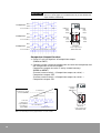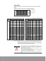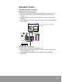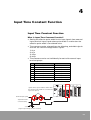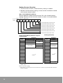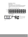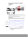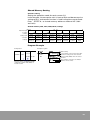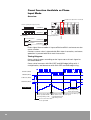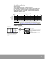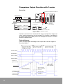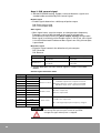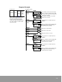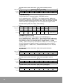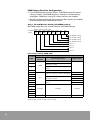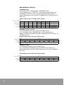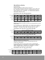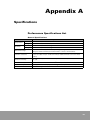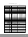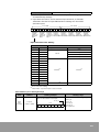
1
SM
Maximum Value for OEMs
NX70 Pulse I/O Unit (4CH)
(NX70-PULSE4)
User Manual
Important User Information
Solid state equipment has operational characteristics differing from those of
electromechanical equipment. Because of these differences, and also
because of the wide variety of uses for solid state equipment, all persons
responsible for applying this equipment must satisfy themselves that each
intended application of this equipment is acceptable.
In no event will OE MAX Controls be responsible or liable for indirect or
consequential damages resulting from the use or application of this
equipment.
The examples and diagrams in this manual are included solely for
illustrative purposes. Because of the many variables and requirements
associated with any particular installation, OE MAX Controls cannot assume
responsibility or liability for actual use based on the examples and
diagrams.
No patent liability is assumed by OE MAX Controls with respect to use of
information, circuits, equipment, or software described in this manual.
Reproduction of the contents of this manual, in whole or in part, without
written permission of OE MAX Controls is prohibited.
Throughout this manual we use notes to make you aware of safety
considerations.
WARNING
Identifies information about practices or circumstances
which may lead to serious personal injury or death, property
damage, or economic loss.
IMPORTANT
Identifies information that is critical for successful
application and understanding of the product.
ATTENTION
Identifies information about practices or circumstances that
can lead to minor personal injury, property damage,
economic loss, or product malfunction. However, depending
on the situation, failure to follow the directions
accompanying this symbol may also lead to serious
consequences.
Contents
1. Pulse I/O Unit Functions ............................................ 9
Features and Functions ................................................................................ 9
Functions of Unit ........................................................................................ 10
Configuration and Limit for Pulse I/O Unit ............................................... 14
Restrictions Due to Combination of Pulse Output Function ................... 14
Parts and Functions .................................................................................... 15
Wiring .......................................................................................................... 17
2. Configuration and Design Verification of the Unit .. 19
Slot No. and I/O Number Allocation Verification ..................................... 19
Embedded Counter..................................................................................... 27
3. General I/O Function................................................ 29
General I/O Function................................................................................... 29
4. Input Time Constant Function................................. 31
Input Time Constant Function ................................................................... 31
Use Input Time Constant Function............................................................ 33
5. High-Speed Counter Function ................................. 35
High-Speed Counter Function ................................................................... 35
Count Function Available as Direction Control Mode ............................. 40
Count Function Available as Individual Input Mode................................ 42
Count Function Available as Phase Input Mode ...................................... 44
6.
Comparison Output Function .................................. 47
Comparison Output Function .................................................................... 47
Comparison Output Function with Counter ............................................. 50
7. Pulse Output Function............................................. 53
Pulse Output Function ................................................................................ 53
Use Pulse Output Function ........................................................................ 57
Use Pulse Output Function (Frequency Change) ..................................... 59
Use Pulse Output Function (Constant Pulse Output)............................... 62
Use Pulse Output Function (Setting Increase/Decrease Position) .......... 67
3
8. PWM Output Function ............................................. 73
PWM Output Function ................................................................................ 73
Use PWM Output Function ........................................................................ 77
9.
Application Examples.............................................. 81
Speed Measuring........................................................................................ 81
Fixed Length Processing ............................................................................ 83
Position Control by Absolute Value .......................................................... 86
Position Control by Data Table .................................................................. 89
Appendix A. Specifications ........................................... 93
Performance Specifications List ................................................................ 93
Appendix B. I/O Contact Points and Memory Map ........ 97
I/O Contact Points ....................................................................................... 97
Shared Memory Areas ............................................................................... 99
4
Safety Instructions
Please read this manual and the related documentation thoroughly
and familiarize yourself with product information, safety instructions
and other directions before installing, operating, performing
inspection and preventive maintenance. Make sure to follow the
directions correctly to ensure normal operation of the product and
your safety.
WARNING
ATTENTION
• If this product is used in a situation that may cause
personal injury and/or significant product damage,
implement safety measures such as use of fault-safe
equipment.
• Do not use this product under any conditions
exposed to explosive gases. It may cause an
explosion.
• Please fasten cables with terminal bolts.
• Do not use the product under conditions that do not
meet correct environmental standards.
• Make sure you connect grounding cables.
• Do not touch terminals when electric current is
flowing.
5
NX 70 Pulse I/O Unit Installation Environment
ATTENTION
Do not install your unit if any of the following
conditions are present:
• Ambient temperature outside the range of 0 to 55 °C
(32 to 131 °F).
• Direct sunlight.
• Humidity outside the range of 30% to 85%
(non-condensing).
• Chemicals that may affect electronic parts.
• Excessive or conductive dust, or salinity.
• High voltage, strong magnetic fields, or strong
electromagnetic influences.
• Direct impact and excessive vibration.
ATTENTION
Precautions for Electrostatic
• Excessive static electricity can be generated in dry
conditions, so please make sure to discharge
electrostatic with other materials like grounded
metal bars before contacting unit
ATTENTION
Cleaning Unit
• Do not use thinners, which can damage or degrade
PCB circuit board.
6
Comparison between High-speed Counter unit (1CH or 2CH) and
Pulse I/O Unit
Comparison item
Number of
channels
Highest
counting speed
High-speed
Counting range
counter
High-speed counter unit
NX70-HSC2
NX70-HSC4
NX70-PULSE4
1CH
2CH
4CH
4CH
Max. 200 KHz
Max. 200 KHz
Max. 100 KHz
24bit signed (Binary format)
(-16,777,216 to +16,777,215)
32bit signed (Binary format)
(-2,147,483,648 to +2,147,483,647)
5µs
2.5µs
Min. input
pulse width
Comparison
output
Input time constant
Pulse I/O unit
NX70-HSC1
2 points,
(C=P, C>P)
4 points,
(C=P, C>P) x 2
8 points, random designation for 8
target values
None
4 µs, 8 µs, 16 µs, 32 µs
(Setting for 2 input units)
Pulse output function
None
None
4CH, 100 KHz
PWM function
None
None
4CH, 30 KHz
Reference Manuals
NX70 Controller User Manual
NX7/NX70 Instruction Set Reference Manual
WinGPC Software User Manual
Click “HELP” on the WinGPC S/W screen or contact your local
distributor.
7
8
1
Pulse I/O Unit Functions
Features and Functions
Features
NX70 PLC Pulse I/O unit is a special unit that provides easy
implementation of pulse output and high-speed counter functions.
The main features of pulse I/O unit include the following.
Pulse I/O unit provides high-speed counter functions with various other
functions as follows:
NX70 PLC
Pulse output unit
(NX70-PULSE4)
It operates as mixed I/O unit.
General I/O Function
(See "Chapter 3")
Set the effective pulse width of input
signal.
Input Time Constant
Function
(See "Chapter 4")
Count pulse number.
Counter Function
(See "Chapter 5")
Compare pulse number and set
value and output the results.
Comparison Output
Function
(See "Chapter 6")
Pulse output.
Pulse Output Function
(See "Chapter 7")
PWM output.
PWM Output Function.
(See "Chapter 8")
Pulse output and PWM output are only available to pulse I/O unit.
Be careful because this function is NOT available for High-performance
High-speed counter unit (4CH).
System Configuration Without Losses
Unit I/O terminals that are not allocated to any function can be used for
general I/O terminal, which enables a single high-speed counter unit to be
used both for counter function and sensor input, providing system
configuration without system resource loss.
Easy position control with a single pulse I/O unit
Pulse I/O unit provides pulse output function. Output pulses are always
known to the Pulse I/O unit, which feature allows you to implement a position
control with a single Pulse I/O unit.
Four 0.8A Outputs
9
Functions of Unit
●
Each function can be operated by shared memory settings.
General I/O Functions
● Pulse I/O unit operates as a 16 In/16 Out mixed I/O unit with its
default setting. By changing the shared memory configuration, you
can configure it as a specialty module, such as high speed counter
or pulse output unit, a 32-point input unit, a 32-point output unit, or
a 16 In/16 Out mixed I/O unit .
● I/O allocation changes depending on unit installation slot.
(Ex.) When unit is installed in slot 0, as for occupied I/O addresses,
R0 to R1 are allocated for input, and R2 to R3 for output. Among
them, word in R0 is designated for input from external terminal
block, and that in R2 for output to external terminal block.
● Function I/O will set as priority when using functions, but for areas
without function allocation, they will be used for general I/O.
Input Time Constant Functions
● Effective pulse width for input signals from I/O connector can be set
by this function.
Input signal whose pulse width is smaller than the effective pulse
width is considered noise.
● Effective pulse width can be set by four constants, in two point units
for I/O connector, as described below.
Effective Pulse Max. count
Width (Wµs)
speed
Setting
Unit
External input terminal
NX70 Pulse output unit
No setting
200 kHz
Group 1 [ I ] A1, A2 (Input allocation R0.0, R0.1)
4
125 kHz
Group 2 [ I ] A3, A4 (Input allocation R0.2, R0.3)
8
62.5 kHz
Group 3 [ I ] A5, A6 (Input allocation R0.4, R0.5)
16
31.2 kHz
Group 4 [ I ] A7, A8 (Input allocation R0.6, R0.7)
32
15.6 kHz
Group 5 [ I ] B1, B2 (Input allocation R0.8, R0.9)
W or more W or more
Group 6 [ I ] B3, B4 (Input allocation R0.10, R0.11)
Group 7 [ I ] B5, B6 (Input allocation R0.12, R0.13)
Group 8 [ I ] B7, B8 (Input allocation R0.14, R0.15)
●
Input time constant function prevents input errors caused by noise
by setting the effective pulse width of input signals. See "Chapter 4"
for detailed settings for input time constant.
R0.0 (Terminal block input)
R0.0 (Signal after time
constant setting)
10
Input signal whose pulse width is smaller
than the effective pulse width is considered
an input error (noise).
Be careful because that the default is set to no time
constant setting.
ATTENTION
High-speed Counter Function
Pulse I/O unit has four high-speed counter channels. There are three
input modes for counting. Input mode can be set for each CH.
Direction control
Counter value changes with pulse train and direction signals.
ta
tb
tc
td
on
IN.A off
IN.B
n
Count number
n+1
n+2
n+1
n
n-1
ta, tb, tc, td ≥ 2.5 µs(1)
Individual input
Count value changes with each input signal at CW and CCW.
ta
tb
tc
on
IN.A off
IN.B
n
Count number
n+1
n+2
n+1
n
n-1
ta, tb, tc ≥ 2.5 µs(1)
Phase differential
Count value changes with the phase differential input on encoder and
others.
ta tb tc td
on
IN.A off
IN.B
Count number
(1)
n
n+1
n+2
n+1
n
ta, tb, tc, td ≥ 2.5 µs(1)
Value for when input time constant (filter) is set to None.
11
IMPORTANT
About multiplication
There are three types of multiplication for phase differential
input mode as following.
IN.A
1 multiplication
IN.B
n
Count number
n+1
n+2
CH0 IN.A
IN.B
Clear
Mask
CH2 IN.A
IN.B
Clear
Mask
CH1 IN.A
IN.B
Clear
Mask
CH3 IN.A
IN.B
Clear
Mask
IN.A
2 multiplication
IN.B
n
Count number
n+1
n+2
n+3
n+4
IN.A
4 multiplication
IN.B
Count number
n n+1 n+2 n+3 n+4 n+5 n+6 n+7 n+8 n+9
NX70 PLC
Pulse output unit
(NX70-PULSE4)
Comparison Output Function
Comparison output
set value (MEMx)
●
Pulse I/O unit has 8 points of comparison output.
(CMP0 to CMP7)
●
Counter current value and comparison set value are compared, and
the comparison results are output.
Comparison output set value is set by shared memory.
(MEM0 to MEM7)
(Counter current value) < (Comparison output set value) →
Comparison output: OFF
(Counter current value) ≥ (Comparison output set value) →
Comparison output: ON
Comparison
Output
(CMP0 to 7)
Coincidence
Counter current
value
Pulse I/O
Comparison
output (CMPx)
Coincidence
signal (EQx)
OFF
ON
No coincidence
Coincidence
Comparison output ON/OFF can also be set as reverse operation.
EQx is an internal processing signal that is not sent outside.
12
NX70 PLC
Pulse output unit
(NX70-PULSE4)
Pulse Output Function
●
Pulse I/O unit has 4CH for pulse output.
●
Max. 100 kHz output and 2 modes of output form as shown below
are available for pulse output function.
Output frequency can be set by 1 Hz unit.
●
Pulse output unit can be input to high-speed counter via internal
connection, providing high-speed processing.
Direction control
Forward direction(+)
PLSx A
OFF
Negative direction(-)
ON
PLSx B
ON
OFF
PLS0 A, PLS0 B
CW-CCW
PLSx A
OFF
Forward direction(+) Negative direction(-) PLS1 A, PLS1 B
PLS2 A, PLS2 B
ON
PLS3 A, PLS3 B
PLSx B
ON
OFF
NX70 PLC
Pulse output unit
(NX70-PULSE4)
PWM Output Function
●
Pulse I/O unit has 4CH for PWM output.
●
Max. 30 kHz is available for PWM output, and Duty can be set by
1% unit.
PWM setting example
Max. 30 kHz
PWM 30%
PWM 60%
30%
60%
on
off
60%
40%
on
off
PWM3
PWM2
PWM1
PWM0
NX70 PLC
Pulse output unit
(NX70-PULSE4)
ATTENTION
Pulse output and PWM output functions are only
available on pulse I/O unit.
13
Configuration and Limit for Pulse I/O Unit
Configuration Limit with Current Consumption
Internal current consumption for Pulse I/O unit is shown below (at 5V).
Be careful when configuring system, not to exceed the total capacity
limit, considering the consumption of other units.
PLC Model
Name
Catalog
number
Current consumption
(5V power)
NX70 PLC
Pulse I/O unit (4CH)
NX70-PULSE4
450 mA
Remarks
Mounting of Pulse I/O Unit
●
For NX70 PLC
Pulse I/O unit can be mounted at any location on the basic
backplane.
But it cannot be mounted on power supply unit or CPU unit slots.
There is no limit to the number of Pulse I/O mounting for NX70 PLC.
Basic backplane
Mountable at any
location
Restrictions Due to Combination of Pulse
Output Function
Pulse I/O unit sends out pulse and PWM outputs from the same CH.
Up to 4CH are available.
When using combination of pulse and PWM outputs, allocate pulse
ahead of PWM as shown in the following table.
Combination
14
Using CH
CH0
CH1
CH2
CH3
1
PWM
PWM
PWM
PWM
2
PLS
PWM
PWM
PWM
3
PLS
PLS
PWM
PWM
4
PLS
PLS
PLS
PWM
5
PLS
PLS
PLS
PLS
Parts and Functions
Parts and Functions
Bottom of Unit
NX70 PLC Pulse
output unit
(NX70-PULSE4)
1. Status LED
Turns on I/O status light at the terminal blocks.
2. Input Connector (NX70 PLC), [ I ]
Relays input signals from an external device to the Pulse I/O unit.
3. Output Connector (NX70 PLC), [ II ]
Relays output signals from the Pulse I/O unit to an external device.
4. Mode Setting Switch is reseved for future use
Mode Setting Switch
Reserved
2
1
ON
15
Status LEDs
Unit LED indicates the I/O status at the terminals. Refer to the table
below.
NX70 Pulse I/O unit allocation table (NX70-PULSE4)
[I]
0
A1
A2
A3
A4
A5
A6
A7
A8
7
8
B1
B2
B3
B4
B5
B6
B7
B8
F
20
A1
A2
A3
A4
A5
A6
A7
A8
27
28
B1
B2
B3
B4
B5
B6
B7
B8
2F
[ II ]
[Unit LED Indicator Window]
NX70 Pulse I/O unit (NX70-PULSE4)
Functions
Functions
LED
LED
Input
[I]
Counter Comparison Pulse
PWM
Output Counter Comparison
Pulse
PWM
A1
R0.0
CH0 IN-A
-
-
-
A1
R2.0
-
[CMP0]
PLS0
direction
-
A2
R0.1
CH0 IN-B
-
-
-
A2
R2.1
-
[CMP1]
PLS1
direction
-
A3
R0.2
CH0 Clear
-
-
-
A3
R2.2
-
[CMP2]
PLS2
direction
-
A4
R0.3
CH0 Mask
-
-
-
A4
R2.3
-
[CMP3]
PLS3
direction
-
A5
R0.4
CH1 IN-A
-
-
-
A5
R2.4
-
[CMP4]
-
-
A6
R0.5
CH1 IN-B
-
-
-
A6
R2.5
-
[CMP5]
-
-
A7
R0.6
CH1 Clear
-
-
-
A7
R2.6
-
[CMP6]
-
-
[ II ]
A8
R0.7
CH1 Mask
-
-
-
A8
R2.7
-
[CMP7]
-
-
B1
R0.8
CH2 IN-A
-
-
-
B1
R2.8
-
-
[PLS0 A]
-
B2
R0.9
CH2 IN-B
-
-
-
B2
R2.9
-
-
[PLS0 B]
-
B3
R0.10
CH2 Clear
-
-
-
B3
R2.10
-
-
[PLS1 A]
-
B4
R0.11
CH2 Mask
-
-
-
B4
R2.11
-
-
[PLS1 B]
-
B5
R0.12
CH3 IN-A
-
-
-
B5
R2.12
-
-
[PLS2 A]
[PWM0]
B6
R0.13
CH3 IN-B
-
-
-
B6
R2.13
-
-
[PLS2 B]
[PWM1]
B7
R0.14
CH3 Clear
-
-
-
B7
R2.14
-
-
[PLS3 A]
[PWM2]
B8
R0.15
CH3 Mask
-
-
-
B8
R2.15
-
-
[PLS3 B]
[PWM3]
- marks: No output allocation
[ ] marks: Indicate the connector pins to which the comparison results are
directly output in order to send to an external device. But the signal
states are saved in the input contacts, R1.0 to R1.7, so that you can
monitor them with the programming software.
ATTENTION
16
• LED indicators may show vibrations when there are
high-speed I/O signals, but it does not indicate any
malfunctions on the unit.
• The numbers described above are I/O numbers with
Pulse I/O unit mounted in slot 0.
I/O number can differ depending on the installation
slot.
Wiring
Terminal Pinouts
Terminal arrangement is common to Pulse I/O unit (4CH) and
High-performance High-speed counter unit (4CH).
[I]
Input part
[ II ]
Output part
[ NX70 Pulse I/O unit (NX70-PULSE4) ]
NOTE
4 (+ COM) points, 2 (+) points, and 2 (0V) points are internally connected,
respectively.
17
Wiring Diagrams
Input Part
Input indicator
LED
Input terminal
Internal Circuit
24V DC
COM terminal
Output Part
Output
indicator
LED
Terminal
Internal Circuit
Output terminal
~
Terminal
18
2
Configuration and Design Verification
of the Unit
Slot No. and I/O Number Allocation
Verification
Occupied I/O Area
As with other I/O units, NX70 Pulse I/O units also use the allocation for
input (R)/output (R).
NX70 Pulse I/O units occupy 32 input (R0.0 to R1.15) and 32 output
(R2.0 to R3.15) points. Occupied I/O area configuration is as follows:
(Ex.) When Pulse I/O unit is installed in slot 0
64 occupied points
32 points input
32 points output
From them, 16 points are
allocated for input connector
and 16 points for output
connector.
Input: R0.0 to R1.15 (R0 to R1),
Output: R2.0 to R3.15 (R2 to R3)
NX70 PLC
Pulse I/O Unit
(NX70-PULSE4)
19
Pulse I/O Unit I/O Allocation Table
Input Allocation, NX70 Pulse I/O Unit (NX70-PULSE4)
Functions
External
Terminal
Input
Counter
Comparison
Pulse
PWM
A1
R0.0
CH0 IN-A
-
-
-
A2
R0.1
CH0 IN-B
-
-
-
A3
R0.2
CH0 Clear
-
-
-
A4
R0.3
CH0 Mask
-
-
-
A5
R0.4
CH1 IN-A
-
-
-
A6
R0.5
CH1 IN-B
-
-
-
External
Terminal
[I]
Unit
Internal
I/O
A7
R0.6
CH1 Clear
-
-
-
A8
R0.7
CH1 Mask
-
-
-
B1
R0.8
CH2 IN-A
-
-
-
B2
R0.9
CH2 IN-B
-
-
-
B3
R0.10
CH2 Clear
-
-
-
B4
R0.11
CH2 Mask
-
-
-
B5
R0.12
CH3 IN-A
-
-
-
B6
R0.13
CH3 IN-B
-
-
-
B7
R0.14
CH3 Clear
-
-
-
B8
R0.15
CH3 Mask
-
-
-
-
R1.0
-
Comparison CMP0
-
-
-
R1.1
-
Comparison CMP1
-
-
-
R1.2
-
Comparison CMP2
-
-
-
R1.3
-
Comparison CMP3
-
-
-
R1.4
-
Comparison CMP4
-
-
-
R1.5
-
Comparison CMP5
-
-
-
R1.6
-
Comparison CMP6
-
-
-
R1.7
-
Comparison CMP7
-
-
-
R1.8
-
-
PLS0 A
-
-
R1.9
-
-
PLS0 B
-
-
R1.10
-
-
PLS1 A
-
-
R1.11
-
-
PLS1 B
-
-
R1.12
-
-
PLS2 A
PWM0
-
R1.13
-
-
PLS2 B
PWM1
-
R1.14
-
-
PLS3 A
PWM2
-
R1.15
-
-
PLS3 B
PWM3
- : No input allocation.
ATTENTION
20
The I/O number allocations above are applied when NX70
PLC Pulse I/O unit (4CH) is installed in slot 0. I/O number can
differ depending on the installation slot.
Detailed Descriptions on Occupied I/O points
External Input
R0.0 to R0.15 .......................Input
Operated as input.
It can be monitored as input even though counter
function is in use.
CHx IN-A, CHx IN-B ............Counter Function
Input count signal of counting operation.
Count signal input is IN-A, IN-B.
There are three input modes: 1) Direction control
2) Individual input and 3) Phase input.
CHx Clear ............................Counter Function
Input when counter current value is to be cleared.
Count current value is cleared to zero (0) with this
input.
CHx Mask ............................Counter Function
Pause counter.
When this input turns on, counter is paused.
Internal input
R1.0 to R1.15 .......................Input
This monitors signals from each function, such as
comparison output.
CMP0 to CMP7 ....................Comparison Output Function
The comparison result of comparison output set
value in shared memory and counter current value
can be monitored by R1.0 to R1.7.
(Counter current value) < (Comparison output set
value) → Comparison output: OFF
(Counter current value) ≥ (Comparison output set
value) → Comparison output: ON
Comparison output ON/OFF can also be set as
reverse operation.
PLSx A, PLSx B ................Pulse Output Function
Pulse signals from pulse output function can
be monitored with R1.8 to R1.15.
This input reflects pulse signals output to I/O
connector as internal input.
PWMx ................................PWM output function
PWM signals from PWM output function can
be monitored with R1.12 to R1.15.
This input reflects PWM signals output to I/O
connector as internal input.
21
Output Allocation, NX70 Pulse I/O unit (NX70-PULSE4)
External
Terminal
[ II ]
Unit Internal
I/O
Functions
External
Terminal
Output
Counter
Comparison
Pulse
PWM
A1
R2.0
-
[Comparison CMP0]
PLS0 direction
-
A2
R2.1
-
[Comparison CMP1]
PLS1 direction
-
A3
R2.2
-
[Comparison CMP2]
PLS2 direction
-
A4
R2.3
-
[Comparison CMP3]
PLS3 direction
-
A5
R2.4
-
[Comparison CMP4]
-
-
A6
R2.5
-
[Comparison CMP5]
-
-
A7
R2.6
-
[Comparison CMP6]
-
-
A8
R2.7
-
[Comparison CMP7]
-
-
B1
R2.8
-
-
[PLS0 A]
-
B2
R2.9
-
-
[PLS0 B]
-
B3
R2.10
-
-
[PLS1 A]
-
B4
R2.11
-
-
[PLS1 B]
-
B5
R2.12
-
-
[PLS2 A]
[PWM0]
B6
R2.13
-
-
[PLS2 B]
[PWM1]
B7
R2.14
-
-
[PLS3 A]
[PWM2]
B8
R2.15
-
-
[PLS3 B]
[PWM3]
-
R3.0
CH0 Soft Clear
-
-
-
-
R3.1
CH0 Soft Mask
-
-
-
-
R3.2
CH1 Soft Clear
-
-
-
-
R3.3
CH1 Soft Mask
-
-
-
-
R3.4
CH2 Soft Clear
-
-
-
-
R3.5
CH2 Soft Mask
-
-
-
-
R3.6
CH3 Soft Clear
-
-
-
-
R3.7
CH3 Soft Mask
-
-
-
-
R3.8
-
-
PLS0 enabled
PWM0 enabled
-
R3.9
-
-
PLS1 enabled
PWM1 enabled
-
R3.10
-
-
PLS2 enabled
PWM2 enabled
-
R3.11
-
-
PLS3 enabled
PWM3 enabled
-
R3.12
-
-
PLS0 start
PWM0 start
-
R3.13
-
-
PLS1 start
PWM1 start
-
R3.14
-
-
PLS2 start
PWM2 start
-
R3.15
-
-
PLS3 start
PWM3 start
- : No output allocation
[ ] : Indicate the connector pins on which the comparison results are directly output in
order to send to an external device. But the signal states are saved in the input
contacts, R1.0 to R1.7, so that you can monitor them with the programming software.
ATTENTION
22
The I/O number allocations above are applied when NX70
PLC Pulse I/O unit (4CH) is installed in slot 0. I/O number can
differ depending on the installation slot.
Detailed Descriptions on Occupied I/O Points
External Output
R2.0 to R2.15 . ....................Output
Operated as output.
But, if there is high-performance output allocation,
high-performance output is sent to I/O connector.
It can be used as internal relay when not being
used for external output.
PLSx direction ...................Pulse Output Function
Pulse output is directed to R2.0 to R2.3.
This output can be used together with comparison
result output CMPx. In that case, comparison
result is sent to I/O connect and pulse can be
directed with this R output.
CMP0 to CMP7 ...................Comparison Output Function
Comparison result output that has been calculated
by comparison output functions.
This output is directly allocated to external output
terminal [ II ] A1 to A8), and its output (R)
(R2.0 to R2.7) can be used for PLS direction or
internal relay. Comparison output can be
monitored by internal input (R) with same name.
PLSx A, PLSx B ................Pulse output function
Pulse generated by pulse output functions is sent
out.
There are A and B types of signal outputs. This
output is directly allocated to external output
terminal ([ II ] B1 to B8), and output (R)
(R2.8 to R2.15) can be used as internal relay.
Comparison output can be monitored by internal
input with the same name (R).
PWMx ...............................PWM Output Functions
PWM signals generated by PWM output functions
are sent out.
This output is directly allocated to external output
terminal ([ II ] B5 to B8), and output (R)
(R2.12 to R2.15) can be used as internal relay.
Comparison output can be monitored with input
with the same name (R).
23
Internal Output
R3.0 to R3.15 .......................Output
This output is a controlling signal for each
function such as counter function.
It can be used as internal relay when not allocated
to any function.
CHx Soft Clear ....................Counter Function
Output when counter current value is to be
cleared.
Counter current value is cleared to zero (0) by this
output (R3.0, R3.2, R3.4, R3.6).
CHx Soft Mask ....................Counter Function
Output for counter pause.
When this output (R3.1, R3.3, R3.5, R3.7) turns on,
counter is paused.
PLSx Enable ......................Pulse Output Function
This signal enables pulse output.
Pulse output is available while this input
(R3.8 to R3.11) is ON.
PLSx start ..........................Pulse Output Function
This signal starts pulse output (R3.12 to
R3.15). Valid only when set to Enable.
PWMx Enable ...................PWM Output Function
This signal enables PWM output.
PWM output is available while this inputs
(R3.8 to R3.11) are ON.
PWMx start .......................PWM Output Function
This signal starts PWM output (R3.12 to
R3.15). Valid only when set to Enable.
24
Verification of Allocated I/O Number and Slot No.
●
I/O number and slot number are necessary for programming.
●
I/O number changes with backplane installation location. Make sure
it is the same as design.
●
For I/O allocation, See "I/O Number Allocation" in Chapter 2 of each
PLC system manual.
I/O Number Allocation Verification
Check the occupied I/O areas of the entire unit where Pulse I/O units
are installed.
(Ex.) When a Pulse I/O unit is installed next to two I/O units on a CPU
backplane
Pulse I/O unit
Slot No.
0
1
2
3
4
CPU backplane
R0.0
to
R3.15
R4.0 R6.0 R10.0 R11.0
to
to
to
to
R5.15 R7.15 R10.15 R11.15
R8.0
to
R9.15
(Ex.) When a Pulse I/O unit is installed next to four I/O units on a CPU
backplane
Pulse I/O unit
Slot No.
R0.0 R2.0 R4.0 R6.0 R8.0
to
to
to
to
to
R1.15 R3.15 R5.15 R7.15 R9.15
R10.0
to
R11.15
25
Verification of Slot No.
When mounted on CPU backplane
The first slot on the right of CPU is 0, and the others are numbered as
their location order.
Pulse I/O unit
Slot No.
CPU backplane
26
0
1
2
3
4
Embedded Counter
Embedded Counter Functions
Embedded Counter Functions
● Input pulse counting functions are embedded in the Pulse I/O unit.
● Counted values are stored in the shared memory areas of each
channel.
● Stored values can be read by a program, so current value can be
checked.
● With comparison functions, external output can be set according to
count value.
High-Speed
Counter
Shared
Memory
The values can be read with ladder
programs.
Current
Value
Pulse train input
Embedded Counter Operation
●
●
●
Count value is set to zero (0) on power off.
Count value (current value) stored in shared memory can be read
with the READ instruction.
Count value (current value) can be modified with the WRITE
instruction.
27
Count Range of the Counter
-2,147,483,648 to +2,147,483,647
(signed 32-bit)
When current value exceeds max.
(min.), it returns to min. (max.)
without error. In this case no error
occurs.
Max. Value=
Min. Value=
Shared Memory Address for Storing Counter Value
Share Memory Address (heximal)
Decimal
Event
HEX
CH0
264, 265
108h, 109h
CH1
266, 267
10Ah, 10Bh
CH2
268, 269
10Ch, 10Dh
CH3
270, 271
10Eh, 10Fh
Current
value count
Signed 32-bit
-2,147,483,648 to +2,147,483,647
Read Current Value
Use the READ instruction to read the count value (current value) from
the shared memory of Pulse I/O unit.
Current Value Input
Use the WRITE instruction to enter the count value (current value) into
the shared memory of Pulse I/O unit.
28
3
General I/O Function
General I/O Function
What is General I/O Function?
●
General I/O function means the digital I/O, represented by input and
output units.
Pulse I/O unit has high-performance functions like counter function,
but I/O without allocations for high-performance functions is used
for digital I/O functions.
●
When used along with input time constant functions, it can be used
as I/O with input time constant functions, which provides highperformance I/O with stronger noise immunity.
External Input External Output
R0.0 to R0.15
R2.0 to R2.15
●
The I/O number allocations above are applied when Pulse I/O unit is
installed in slot 0.
29
How to use General I/O Function?
All I/O of Pulse I/O unit can be used for general I/O function. But when
high-performance functions are allocated, such as high-speed counter
function, the allocated functions have higher priority.
Using Method
●
Special settings such as mode setting switch or shared memory
settings are not needed for general I/O unit usage.
Use with initial setting.
●
When Pulse I/O unit is installed in slot 0, input R0.0 to R.15 and
output R2.0 to R2.15 can be used for external I/O contacts.
IMPORTANT
30
Terminals not allocated for functions can be used for general
I/O, which provides system configuration without losses,
including counter functions and sensor input only with a
single Pulse I/O unit.
4
Input Time Constant Function
Input Time Constant Function
What is Input Time Constant Function?
●
Setting the effective pulse width for the input signals from external
input terminal. Input signal whose pulse width is smaller than the
effective pulse width is considered noise.
●
Time constant can be selected from the following, and width signals
over the set value are recognized as signals.
1) 4 µs
2) 8 µs
3) 16 µs
4) 32 µs
●
Time constant can be set individually for each of 8 external input
terminal groups.
External input terminal [ I ]
Input allocation
1)
A1, A2
R0.0, R0.1
2)
A3, A4
R0.2, R0.3
3)
A5, A6
R0.4, R0.5
4)
A7, A8
R0.6, R0.7
5)
B1, B2
R0.8, R0.9
6)
B3, B4
R0.10, R0.11
7)
B5, B6
R0.12, R0.13
8)
B7, B8
R0.14, R0.15
(NX70 Pulse I/O unit NX70-PULSE4)
Signals whose pulse width is smaller than
the effective pulse width are considered as
input error (noise).
Terminal input signal
Signals after time
constant setting
set time constant
(Signal output delays as time constant)
31
Input constant functions can be used along with counter
function.
IMPORTANT
Input Time Constant Functions
To use input time constant functions, shared memory setting is
needed.
●
Using Method
Input time b31~
constant b28
setting
●
Set input constant for 8 external input terminal groups by setting
shared memory.
●
Input time constant is set for external output terminal, so function
allocations for each of input R0.0 to R0.15 settings are also valid.
(Counter input)
b27~
b24
b23~
b20
b19~
b16
b15~
b12
b11~
b8
b7~
b4
b3~
b0
Input time constant settings for R0.0 and R0.1
Input time constant settings for R0.2 and R0.3
Input time constant settings for R0.4 and R0.5
Input time constant settings for R0.6 and R0.7
Input time constant settings for R0.8 and R0.9
Input time constant settings for R0.10 and R0.11
Input time constant settings for R0.12 and R0.13
Input time constant settings for R0.14 and R0.15
Input Time Constant Setting
Set value
(HEX)
Functions
Input time constant
Effective pulse width
0
1
2
4 µs
Used
3
8 µs
16 µs
32 µs
4
5
6
7
8
9
Invalid(1)
Invalid(1)
A
B
C
D
E
F
32
Unused(2)
(1)
Do not use this setting.
(2)
Initial value on power input is set to unused.
-
Make sure to access shared memory by 2 word units.
ATTENTION
Use Input Time Constant Function
Overview
Install Pulse unit in
slot No. 0
Ignored as noise
Terminal input
signal
After time constant
processing
Ignored as noise
Terminal input
signal
After time constant
processing
Set time constant for R0.0, R0.1 input, and ignore signals outside the
width as noise.
Shared Memory Setting
Time constant setting
Set input time constant.
In the example, time constant of 16 µs is set for R0.0 and R0.1 input.
Therefore, enter 「FFFFFFF2」 into shared memory address 13Ch and
13Dh.
Shared memory 316, 317 (13Ch, 13Dh) settings
(bit) 32
R0.15,
External input
R0.14
Set value
F
Settings
Unused
R0.13,
R0.12
16 15
R0.9,
R0.7,
R0.8
R0.6
R0.11,
R0.10
0
R0.5,
R0.4
R0.3,
R0.2
R0.1,
R0.0
F
F
F
F
F
F
2
Unused
Unused
Unused
Unused
Unused
Unused
16 µs
NOTE See "Shared Memory Areas" in Appendix A for shared memory addresses.
Program Example
Configuration
POWER
CPU
Example Program
F001.00
NX70
Pulse4
Slot#0
Slot#1
Input the values of W100 and W101
of CPU into address 316 (13Ch) of
Pulse4 module (input constant
setting)
First
1Scan
ON
DLET
D = W100
S = $FFFFFFF2
WRITE
TO = 0 : 316
SZ = 2
FR = W100
Data setting
Slot number of the mounted module
Write to shared memory address
316 to 317 (13Ch to 13Dh) (input
constant setting)
The number of words to be written
Address area to write
33
34
5
High-Speed Counter Function
High-Speed Counter Function
What is Counter Function?
●
Counter function counts the input pulse number and reflects it into
the current value. Also, it sets the offset value by recording data into
the current value.
●
Pulse I/O unit has 4 channels of 2 phase input counter. There are
three types of 2 phase input mode as follows.
1) Direction Control Mode
2) Individual Input Mode
3) Phase Input Mode
●
Particular to Pulse I/O unit, the connection point (condition) of pulse
signals to be counted can be selected.
1) Counting inputs from I/O connector.
2) Pulses generated from pulse output or PWM output function
are counted via internal connection.
Input pulse
Shared
memory
The count value of pulse number is stored
in the shared memory as current value.
Counter
Current
value
1) Internal counting of
pulses output from unit
2) Count input pulses
35
Setting Counter Function
●
To use counter function, shared memory setting is needed.
●
Besides shared memory setting, counter can be masked or cleared
with counter control signal.
Step 1. Shared Memory Setting
Set the operation mode for each counter CH in the shared memory
settings. Set the counter functions mode as shown in the table below.
Address: 256, 257 (100h, 101h)
Counter
setting
b31~
b28
b27~
b24
b23~
b20
b19~
b16
b15~
b12
b11~
b8
b7~
b4
b3~
b0
Counter CH0 setting (used/unused)
Counter CH0 setting (input mode)
Counter CH1 setting (used/unused)
Counter CH1 setting (input mode)
Counter CH2 setting (used/unused)
Counter CH2 setting (input mode)
Counter CH3 setting (used/unused)
Counter CH3 setting (input mode)
Setting (Input Mode): Effective only for
terminal input
Set value
(HEX)
Functions
Terminal input mode
(3)
0
Direction control
1
Individual input
2
3
Phase input
4
N/A
Set value
(HEX)
Functions
0
Used
(Terminal input)
1
1 multiplication
2
2 multiplications
3
4 multiplications
4
5
5
6
6
7
7
8
8
9
A
36
Multiplication
Setting (Function)
9
Invalid(2)
A
B
B
C
C
D
D
E
E
F
F
Counter
Used (Internal
connection)(1)
Invalid(2)
Unused(3)
(1)
Used when counting the number of output pulses via internal connection to pulse or
PWM output.
(2)
Do not use this setting.
(3)
Initial values on power input are set as direction control for input mode and unused for
function setting.
ATTENTION
• Make sure to access shared memory by 2 word units.
• Internal connection between the counter and pulse/PWM
output is fixed on the CHs for counter and pulse/PWM
output.
• When pulse/PWM output are internally connected to
counter, the input mode of counter is automatically
configured to the input mode. Be careful that previously
configured counter input mode is ignored.
Step 2. Counter Control Signal
●
Counter functions can set mask or clear with counter control signal.
●
There are two types of counter control signals as follows: Control
by external input terminal and Control by programming. Both
allow counter control.
Control by external input terminal
Control Signals (External input terminal)
External terminal
[I]
Input
allocation
A3
R0.2
A4
R0.3
A7
R0.6
A8
R0.7
B3
R0.10
B4
R0.11
B7
R0.14
B8
R0.15
Function
Subject
counter
CH0
CH1
CH2
CH3
Control
events
Remarks
Clear
Count current value is cleared to 0 with input ON.
Mask
Count is paused with input ON.
Clear
Count current value is cleared to 0 with input ON.
Mask
Count is paused with input ON.
Clear
Count current value is cleared to 0 with input ON.
Mask
Count is paused with input ON.
Clear
Count current value is cleared to 0 with input ON.
Mask
Count is paused with input ON.
Control by programming
Control Signals (Internal output terminal)
Output
allocation
R3.0
R3.1
R3.2
R3.3
R3.4
R3.5
R3.6
R3.7
Function
Subject counter
CH0
CH1
CH2
CH3
ATTENTION
Control events
Remarks
Clear
Count current value is cleared to 0 with output ON.
Mask
Count is paused with output ON.
Clear
Count current value is cleared to 0 with output ON.
Mask
Count is paused with output ON.
Clear
Count current value is cleared to 0 with output ON.
Mask
Count is paused with output ON.
Clear
Count current value is cleared to 0 with output ON.
Mask
Count is paused with output ON.
Be careful that when counter output is internally connected,
the control input (by external terminal) from I/O connector is
ignored.
37
Read Counter Current Value
●
Current value of each counter is stored in shared memory as
described below.
●
Use the READ instruction (reading data from high-performance
units) to read the current value by 2 word units.
Address: 264, 265 (108h, 109h)
Counter CH0 Current value
K-2,147,483,648 to K+2,147,483,647
Address: 266, 267 (10Ah, 10Bh)
Counter CH1 Current value
K-2,147,483,648 to K+2,147,483,647
Address: 268, 269 (10Ch, 10Dh)
Counter CH2 Current value
K-2,147,483,648 to K+2,147,483,647
Address: 270, 271 (10Eh, 10Fh)
Counter CH3 Current value
K-2,147,483,648 to K+2,147,483,647
Program Example
Configuration
POWER
CPU
Example Program
M000.00
NX70
Pulse4
Slot#0
Slot#1
Input the value of address 264 of
Pulse4 module into W0000 and
W0001 of CPU
38
READ
TO = W0
SZ = 2
FR = 0 : 264
Address where to store the read
value
The number of words to read
Read from the mounted module
Starting address of the shared
memory
Slot number of the mounted module
Current Value Input
●
Current value of each counter is stored in shared memory as
described below.
●
Enter current value by 2 word units, using the WRITE instruction
(data writing at high-performance unit).
Address: 264, 265 (108h, 109h)
Counter CH0 Current value
K-2,147,483,648 to K+2,147,483,647
Address: 266, 267 (10Ah, 10Bh)
Counter CH1 Current value
K-2,147,483,648 to K+2,147,483,647
Address: 268, 269 (10Ch, 10Dh)
Counter CH2 Current value
K-2,147,483,648 to K+2,147,483,647
Address: 270, 271 (10Eh, 10Fh)
Counter CH3 Current value
IMPORTANT
K-2,147,483,648 to K+2,147,483,647
Counter offset value can be set by counter current value
input.
Program Example
Configuration
POWER
CPU
Example Program
M000.00
NX70
Pulse4
Slot#0
DLET
WRITE
Data setting
Slot number of the mounted module
Write to the mounted Pulse module
shared memory address 264 (108h)
TO = 0 : 264
SZ = 2
FR = W20
The number of words to be written
Address area to write
D = W20
S = 6400
Slot#1
Input the values of W20 and W21 of
CPU into address 264 (108h) of
Pulse4 module (CH0 result value)
39
Count Function Available as Direction
Control Mode
Overview
Install Pulse unit in slot No.0
Pulse train input
(CH0 IN-A)
Direction control signal input
(CH0 IN-B)
Occupied I/O areasa
0V (24V DC)
Clear instruction
R0
R1
R2
R3
(CH0 clear)
Mask instruction
(CH0 Mask)
Input pulse train in R0.0 and direction control signal in R0.1 and
measure the count number.
Counter current value is cleared with R0.2 clear instruction, and count
operation is paused with R0.3 mask instruction.
Timing Diagram
Count value changes according to the input status of each signal as
illustrated below. Count value changes at the pulse input edge rise
time.
CH0 IN-A (R0.0)
CH0 IN-B (R0.1)
CH0 Clear (R0.2)
CH0 Mask (R0.3)
Count value
Count stops while
mask signal is ON.
Count increases with R0.0 Count decreases
with direction
pulse edge rising and
control ON.
direction control OFF.
Reset count value with
clear signal ON.
40
Count increases with
direction control OFF.
Shared Memory Setting
Counter setting
Setting the operation mode for each counter CH.
In the example, pulse train is input to R0.0 and direction control signal
to R0.1, and counter function is used in direction control mode. Enter
「FFFFFF00」 to shared memory addresses 256 and 257 (100h and
101h).
Shared memory 256, 257 (100h,101h) settings
(bit) 32
External input
Counter
number
R0.12
R0.9
Input
mode
Functions
setting
Set value
F
F
Unused
0
R0.8
R0.5
Input
mode
Functions
setting
F
F
CH3
Setting item
Settings
16 15
R0.13
R0.4
R0.1
Input
mode
Functions
setting
Input
mode
F
F
0
0
Unused
Direction
control
Terminal
Input
CH2
Unused
Unused
CH1
Unused
Unused
R0.0
CH0
Functions
setting
Program Example
Configuration
POWER
CPU
Example Program
F001.00
NX70
Pulse4
Slot#0
Slot#1
Input the values of W100 and W101
of CPU into address 256 (109h) of
Pulse4 module (counter function
setting)
First
1Scan
ON
DLET
WRITE
Data setting
Slot number of the mounted module
Write to the mounted Pulse module
shared memory address 265 (109h)
TO = 0 : 256
SZ = 2
FR = W100
The number of words to be written
Address area to write
D = W100
S = $FFFFFF00
41
Count Function Available as Individual
Input Mode
Overview
Install Pulse I/O unit in slot No.0
Increase pulse input
(CH0 IN-A)
Decrease pulse input
(CH0 IN-B)
Occupied I/O areas
0V (24V DC)
Clear instruction
R0
R1
R2
R3
(CH0 clear)
Mask instruction
(CH0 Mask)
Input increase pulse in R0.0 and decrease pulse signal in R0.1 and
measure the count number.
Counter current value is cleared with R0.2 clear instruction, and count
operation is paused with R0.3 mask instruction.
Timing Diagram
Count value changes according to the input status of each signal as
illustrated below. Count value changes at the pulse input edge rise
time.
CH0 IN-A (R0.0)
CH0 IN-B (R0.1)
CH0 Clear (R0.2)
CH0 Mask (R0.3)
Count value
Count stops while
mask signal is ON.
Count increases with R0.0 Count decreases
with R0.1 input
pulse edge rising and
direction control OFF.
Reset count value with
clear signal ON.
42
Count increases with
R0.0 input
Shared Memory Setting
Counter setting
Setting the operation mode for each counter CH.
In the example, increase pulse train is input to R0.0 and decrease pulse
setting to R0.1, and counter function is used in direction control mode.
Enter 「FFFFFF10」 to shared memory addresses 256 and 257 (100h
and 101h).
Shared memory 256, 257 (100h,101h) settings
(bit) 32
External input
Counter
number
R0.12
R0.9
Input
mode
Functions
setting
Set value
F
F
Unused
0
R0.8
R0.5
Input
mode
Functions
setting
F
F
CH3
Setting item
Settings
16 15
R0.13
R0.4
R0.1
Input
mode
Functions
setting
Input
mode
F
F
0
0
Unused
Direction
control
Terminal
Input
CH2
Unused
Unused
CH1
Unused
Unused
R0.0
CH0
Functions
setting
Program Example
Configuration
POWER
CPU
Example Program
F001.00
NX70
Pulse4
Slot#0
Slot#1
Input the values of W100 and W101
of CPU into address 256 (100h) of
Pulse4 module
First
1Scan
ON
DLET
D = W100
S = $FFFFFF10
WRITE
TO = 0 : 256
SZ = 2
FR = W100
Data setting
Slot number of the mounted module
Function setting area of the shared
memory 256 (100h) of the mounted
module
The number of words to be written
Address area to write
43
Count Function Available as Phase
Input Mode
Overview
Install Pulse I/O unit in slot No.0
Phase signal pulse input (on A)
(CH0 IN-A)
Phase signal pulse input (on B)
(CH0 IN-B)
Occupied I/O areas
0V (24V DC)
Clear instruction
Mask instruction
R0
R1
R2
R3
(CH0 clear)
(CH0 Mask)
Phase signal from encoder is input to R0.0 and R0.1 and measures the
count number.
Counter current value is cleared with R0.2 clear instruction, and count
operation is paused with R0.3 mask instruction.
Timing Diagram
Count value changes according to the input status of each signal as
illustrated below.
Count value increases with IN-A OFF and IN-B edge falling with 1
multiplication, and decreases with IN-A OFF and IN-B edge rising.
CH0 IN-A (R0.0)
CH0 IN-B (R0.1)
CH0 Clear (R0.2)
CH0 Mask (R0.3)
Count value
Count stops while
mask signal is ON.
Count increases with up Count decreases
Count increases with up
with down count
count input (IN-A OFF
count input
input (IN-A OFF and
and edge falling on B)
edge rising on B)
Reset count value with
clear signal ON
44
Shared Memory Setting
Counter setting
Setting the operation mode for each counter CH.
In the example, the phase signal from encoder is input to R0.0 and
R0.1, and counter function is used in 1 multiplication phase input
mode, therefore, enter 「FFFFFF20」 to shared memory addresses
256 and 257 (100h and 101h).
Shared memory 256, 257 (100h,101h) settings
(bit) 32
External input
R0.13
R0.9
Input
mode
Functions
setting
F
F
Counter
number
Set value
Unused
0
R0.8
R0.5
Input
mode
Functions
setting
F
F
CH3
Setting item
Settings
16 15
R0.12
R0.4
R0.1
Input
mode
Functions
setting
Input
mode
F
F
2
0
Unused
Phase
Input
Terminal
Input
CH2
Unused
IMPORTANT
Unused
CH1
Unused
Unused
R0.0
CH0
Functions
setting
In phase differential input mode, the input pulse
magnification can be changed with multiplication function.
See "High-speed Counter Function" in Chapter 1 for details.
Program Example
Configuration
POWER
CPU
Example Program
F001.00
NX70
Pulse4
Slot#0
Slot#1
Input the values of W100 and W101
of CPU into address 256 (100h) of
Pulse4 module (counter function
setting)
First
1Scan
ON
DLET
Data setting
D = W100
S = $FFFFFF20
Slot number of the mounted module
WRITE
TO = 0 : 256
SZ = 2
FR = W100
Function setting area of the shared
memory 256 (100h) of the mounted
module
The number of words to be written
Address area to write
45
46
6
Comparison Output Function
Comparison Output Function
What is Comparison Output Function?
●
Compare the comparison output set value and counter current
value, and the comparison result is output.
Comparison result output [CMPx]:
Comparison output set value ≤ Counter current value
●
Comparison result output can be selected from either ON when
current value < set value or current value ≥ set value.
●
For Pulse I/O unit, 8 types of comparison output set values can be
set, and the comparison counter channels can also be freely
selected. Therefore, if all comparison output set values are set to a
single counter, a maximum of 8 level comparisons are available.
Comparison
output set
value (MEMx)
Coincidence
Counter
current
value
Pulse I/O
Comparison
output (CMPx)
OFF
Coincidence
signal (EQx)
No coincidence
ON
Coincidence
Counter current value is compared with pre-set
comparison output set value, and the result is
output.
EQx is an internal processing signal that is not
sent outside.
Count input pulses
47
Setting Comparison Output Function
To use comparison output function, Step 1. Shared Memory Setting for
Comparison Output Set Value and Step 2. Shared Memory Setting for
Comparison Output Point are needed.
Step 1. Shared Memory Setting for Comparison Output Set Value
Set the comparison output set value to be compared with counter
current value.
Address: 288, 289 (120h, 121h)
Comparison output set
value (for CMP0)
MEM0
Comparison output set
value (for CMP1)
MEM1
Comparison output set
value (for CMP2)
MEM2
Comparison output set
value (for CMP3)
MEM3
Comparison output set
value (for CMP4)
MEM4
Comparison output set
value (for CMP5)
MEM5
Comparison output set
value (for CMP6)
MEM6
Comparison output set
value (for CMP7)
MEM7
K-2,147,483,648 to K+2,147,483,647
Address: 290, 291 (122h, 123h)
K-2,147,483,648 to K+2,147,483,647
Address: 292, 293 (124h, 125h)
K-2,147,483,648 to K+2,147,483,647
Address: 294, 295 (126h, 127h)
K-2,147,483,648 to K+2,147,483,647
Address: 296, 297 (128h, 129h)
K-2,147,483,648 to K+2,147,483,647
Address: 298, 299 (12Ah, 12Bh)
K-2,147,483,648 to K+2,147,483,647
Address: 300, 301 (12Ch, 12Dh)
K-2,147,483,648 to K+2,147,483,647
Address: 302, 303 (12Eh, 12Fh)
ATTENTION
K-2,147,483,648 to K+2,147,483,647
Make sure to access shared memory by 2 word unit.
NOTE See "Shared Memory Areas" in Appendix A for shared memory addresses.
48
Step 2. Shared Memory Setting for Comparison Output Point
Select the counter channel number and output logic for each
comparison output point.
Address: 260, 261 (104h, 105h)
b31~
b28
Comparison
output setting
b27~
b24
b23~
b20
b19~
b16
b15~
b12
b11~
b8
b7~
b4
b3~
b0
Comparison output CMP0 setting
Comparison output CMP1 setting
Comparison output CMP2 setting
Comparison output CMP3 setting
Comparison output CMP4 setting
Comparison output CMP5 setting
Comparison output CMP6 setting
Comparison output CMP7 setting
Comparison Output Setting
Set
value
(HEX)
Functions
Comparison
output
function
Counter CH to be
compared
Output logic
0
CH0
1
ON when current value < set value
2
3
5
CH0
ON when current value ≥ set value
6
CH2
CH3
Used
4
CH1
7
CH1
CH2
CH3
8
9
A
B
Invalid(1)
Invalid(1)
Unused(2)
-
C
D
E
F
(1)
(2)
Do not use this setting.
Initial values on power input are set as unused.
ATTENTION
• Make sure to access shared memory by 2 word unit.
• When using this setting regardless of counter function use
setting (ON/OFF), be careful that comparison output set
value and counter current value are compared.
• When setting the comparison output function, make sure
to first set shared memory for Comparison Output Set
Value. Otherwise, coincidence output is generated at the
time of data setting if the comparison output condition is
met, as in the case that counter initial value and
comparison output set value are both 0.
NOTE See "Shared Memory Areas" in Appendix A for shared memory addresses.
49
Comparison Output Function with Counter
Overview
Install Pulse I/O unit in slot No.0
Pulse train input
(CH0 IN-A)
Direction control signal input
(CH0 IN-B)
Occupied I/O areas
0V (24V DC)
Clear instruction
(CH0 clear)
Mask instruction
(CH0 Mask)
Comparison
coincidence signal
Current
value
Set
value
Comparison
coincidence
output (CMP0)
R0
R1
R2
R3
CMP0
When counter current value coincides with
set value, and the comparison result is
output on CMP0.
Counter current value is compared with pre-set comparison output set
value, and the comparison result is output. This function is available in
all counter operation modes, but in this example the counter is used in
direction control mode.
Timing Diagram
Count value changes according to the input status of each signal as
illustrated below.
Count increases with
R0.0 pulse edge rising
and direction control
Count decreases with
direction control ON.
Count increases with
direction control OFF.
CH0 IN-A (R0.0)
CH0 IN-B (R0.1)
CH0 Clear (R0.2)
CH0 Mask (R0.3)
Comparison
output set value
Count stops on
mask signal ON
Count value
Reset count value
with clear signal ON.
Comparison output
point CMP0 (R2.0)
Coincidence EQ0
(Internal signal)
50
CMP signal ON
when coincidence
or excess.
EQ signal ON
only on
coincidence
Shared Memory Setting
Counter Setting
Setting the operation mode for each counter CH.
In the example, pulse train is input to R0.0 and direction control signal
to R0.1, and counter function is used in direction control mode. Enter
「FFFFFF00」 to shared memory addresses 256 and 257 (100h and
101h).
Shared Memory 256, 257 (100h,101h) Settings
(bit) 32
16 15
External input
Counter
number
R0.13
Setting item
R0.12
R0.9
Input
mode
Functions
setting
Settings
R0.5
Input
mode
Functions
setting
F
F
F
F
CH3
Set value
Unused
0
R0.8
R0.4
R0.1
Input
mode
Functions
setting
Input
mode
F
F
0
0
Unused
Direction
Control
Terminal
Input
CH2
Unused
Unused
CH1
Unused
Unused
R0.0
CH0
Functions
setting
Setting the Comparison Output Set Value
Setting the comparison output set value to be compared with Counter
current value. In the example, the comparison result is output on
CMP0 when counter current value is 6. Enter 「K6(H6)」 in shared
memory addresses 288, 289 (120h, 121h).
Shared Memory 288, 289 (120h, 121h) Settings
(bit) 32
Setting item
Set value
Settings
16 15
0
Comparison output set value (CMP0)
0
0
0
0
0
0
0
6
K6
51
Setting the Comparison Output Point
Select the counter channel number and output logic for each
comparison output point.
In the example, counter current value at CH0 is compared with
comparison output set value and the comparison result is output on
CMP0. Therefore, enter 「FFFFFFF4」 in shared memory addresses
260 and 261 (104h and 105h).
Shared Memory 260, 261 (104h, 105h) Settings
(bit) 32
Comparison input
CMP7
16 15
CMP6
CMP5
CMP4
0
CMP3
CMP2
CMP1
CMP0
Set value
F
F
F
F
F
F
F
4
Settings
Unused
Unused
Unused
Unused
Unused
Unused
Unused
CH0 Comparison(1)
(1)
CMP0 is ON when current value ≥ set value
.
ATTENTION
When setting the comparison output function, make sure to
first set shared memory for Comparison Output Set Value.
Otherwise, coincidence output is generated at the time of
data setting if the comparison output condition is met, as in
the case that counter initial value and comparison output set
value are both 0.
Program Example
Configuration
POWER
CPU
Example Program for comparison output function
F001.00
NX70
Pulse4
Slot#0
Slot#1
Write set value into addresses 256
and 257 (100h and 101h), 288 and
289 (120h and 121h), and 260 and
261 (104h and 105h) of Pulse4
module
First
1Scan
ON
F001.00
DLET
D = W100
S = $FFFFFF00
Data setting (W100 and W101)
Slot number of the mounted module
WRITE
Write to address 256 (100h) (counter
function setting)
TO = 0 : 256
SZ = 2
FR = W100
The number of words to be written
Address area to write
DLET
D = W102
S=6
Data setting (W102 and W103)
WRITE
TO = 0 : 288
SZ = 2
FR = W102
F001.00
Store the values of W102 and W103
into address 288 (120h) (comparison
output set value)
DLET
D = W104
S = $FFFFFFF4
Data setting (W104 and W105)
WRITE
TO = 0 : 260
SZ = 2
FR = W104
52
Store the values of W104 and W105
into address 260 (104h) (comparison
output set value)
7
Pulse Output Function
Pulse Output Function
What is Pulse Output Function?
●
Pulse output function sends out waves at a frequency randomly
selected from 1 Hz to 100 kHz range.
Setting unit is 1 Hz.
●
There are two output modes as follows:
1) Direction control
2) Individual output
●
In addition, Pulse I/O unit provides up to 4CH for pulse output.
But user must choose between pulse output and PWM output, so if
PWM is selected, the number of channels for pulse output is
decreased.
Shared memory
Output
pulse
setting
Settings for pulse output, such as output
frequency, are configured in shared memory.
Current
value
Enter PLS
control signal
After shared memory data is configured,
pulse output starts when PLS control
signal is turned on by I/O operation.
• Enable signal
• Start signal
• Direction signal
ATTENTION
Pulse output (pulse, PWM) consists of 4CH as described
below.
• CH 0: PLS0 output or PWM0 output
• CH 1: PLS1 output or PWM1 output
• CH 2: PLS2 output or PWM2 output
• CH 3: PLS3 output or PWM3 output
53
Setting Pulse output Function
●
To use pulse output function, Step 1. Shared memory PLS/PWM
setting and Step 2. Shared memory PLS/PWM frequency setting are
needed.
●
Beside shared memory setting, Enable start and direction signals
are needed to be controlled with PLS control signal.
Step 1. Shared memory setting (PLS/PWM setting)
Set PWM output form by shared memory PLS/PWM settings.
The Same settings apply when PWM output is selected by pulse
function.
Address: 320, 321 (140h, 141h)
PLS/PWM b31~
Setting
b28
b27~
b24
b23~
b20
b19~
b16
b15~
b12
b11~
b8
b7~
b4
b3~
b0
PLS 0/PWM 0 setting
PLS 1/PWM 1 setting
PLS 2/PWM 2 setting
PLS 3/PWM 3 setting
Unused
Unused
Unused
Unused
Pulse output setting (PWM, PLS)
Set value
(HEX)
Functions
Pulse
function
Data change timing
0
Refresh on edge rise of PLSx start signal
1
Edge rise of PLSx start signal, or
comparison output
PWM
2
Edge rise of PLSx start signal, or data
refresh
3
Reserved area
4
Refresh on edge rise of PLSx start signal
5
6
7
PLS
8
Edge rise of PLSx start signal, or
comparison output
Edge rise of PLSx start signal, or data
refresh
9
Output mode
-
Direction control
Individual output
Direction control
Individual output
Direction control
Individual output
A
B
C
Invalid(1)
Invalid(1)
Invalid(1)
Not used(2)
-
-
D
E
F
54
(1)
Do not use this setting.
(2)
Initial value on power input is set to unused.
ATTENTION
Make sure to access shared memory by 2 word unit.
NOTE See "PLS/PWM Flag" in Appendix B for shared memory addresses.
Step 2. Shared memory setting (PLS/PWM frequency setting)
●
Configure frequency of output pulses after PLS/PWM setting of
shared memory.
●
Frequency is set within the range of 1 Hz to 100 kHz by 1 Hz unit.
Output turns OFF (pulse stop) when frequency setting exceeds
131.072 kHz.
●
When frequency is set to 0 Hz and data is refreshed, pulse output is
stopped.
Address: 328, 329 (148h, 149h)
PLS 0/PWM 0
frequency setting
PLS: K1 to K100000
Address: 330, 331 (14Ah, 14Bh)
PLS 1/PWM 1
frequency setting
PLS 2/PWM 2
frequency setting
PLS: K1 to K100000
Address: 332, 333 (14Ch, 14Dh)
PLS: K1 to K100000
Address: 334, 335 (14Eh, 14Fh)
PLS 3/PWM 3
frequency setting
ATTENTION
PLS: K1 to K100000
• Make sure to access shared memory by 2 word unit.
• On shared memory, PLS/PWM frequency setting should
be located after PLS/PWM setting.
If not, it may not work properly.
• Do not set a value out of the permitted range. It may cause
errors.
• Error detection upper limit of the unit is 1048.575 kHz.
(1048.575 kHz = FFFFFh)
When setting exceeds the limit, the value based on the
lower 20-bit is applied.
NOTE •
•
PLS/PWM flag is prepared at shared memory addresses 322 and 323 (142h and
143h). Pulse output can be monitored by reading the flag in these addresses.
See “PLS/PWM Flag” in Appendix B for details.
See "Shared Memory Areas" in Appendix A for shared memory addresses.
55
Step 3. PLS control signal
●
Beside PLS/PWM setting, Enable, start and direction signals are
needed to be controlled by PLS control signal.
Enable signal
→ Enable signal determines valid/stop of pulse output.
ON: Pulse output valid
OFF: Pulse output stop
Start signal
→ Start signal starts up pulse output, or change output frequency.
Frequency can also be changed at the time of comparison
coincidence or data refresh, by Pulse output setting configuration.
Start signal is valid only when Enable signal is ON. If not, start signal
is invalid. When both Enable and Start signals are ON, pulse output
is permitted.
Direction signal
→ Direction signal controls the direction of pulse output.
OFF: Forward
ON: Reverse
Direction signal
Direction control output
Individual output
OFF (Forward)
Pulse output from PLSx A
PLSx B OFF
Pulse output from PLSx A
PLSx B OFF
ON (Reverse)
Pulse output from PLSx A
PLSx B ON
Pulse output from PLSx B
PLSx A OFF
●
Output allocation for each control signal is shown in the table
below.
Control signal allocation table
Output
Functions
Allocation
Pulse output CH
R2.0
PLS0
R2.1
PLS1
R2.2
PLS2
R2.3
PLS3
R3.8
PLS0
R3.9
PLS1
R3.10
PLS2
R3.11
PLS3
R3.12
PLS0
R3.13
PLS1
R3.14
PLS2
R3.15
PLS3
Control events
Direction control
Enable control
Start control
ATTENTION
56
Remarks
OFF: Forward Direction control output: PLSx B OFF
Individual output: Pulse output from PLSx A
ON: Reverse Direction control output: PLSx B ON
Individual output: Pulse output from PLSx B
OFF: Pulse output stop
ON: Pulse output valid
First ON: Pulse output start
OFF → ON edge: Output pulse frequency changed
Direction signal can be changed even during pulse output,
but timing with pulse output cannot be specified.
Change the signal when pulse is stopped.
Use Pulse Output Function
Overview
Install Pulse I/O unit in slot No. 0
32 points input unit
0V (24V DC)
Direction signal
(PLS0 direction)
Enable signal
(PLS0 Enable)
Enable input (PLS0)
Start input (PLS0)
Start signal
(PLS0 start)
Direction input (PLS0)
Occupied I/O areas
R0
R1
R2
R3
R4
R5
Pulse train output
Pulse output (PLS0 A)
Direction control signal output
Pulse output (PLS0 B)
Sending pulse output in direction control mode.
Turn ON Enable input at R4.0 and Start input. Pulse output starts at
R2.8 and R2.9 (PLS0).
When direction input at R4.2 is ON, pulse changes to reverse direction.
Timing Diagram
Pulse output changes in reference to the input status of each signal as
illustrated below.
PLS0 Enable signal
(R4.0, R3.8)
Pulse output starts when edge rise of Start signal is
detected while Enable signal is ON.
PLS0 Start signal
(R4.1, R3.12)
When direction changes, 1 pulse
is deleted.
PLS0 Direction
signal (R4.2, R2.0)
PLS0 A Pulse
output (R2.8)
PLS0 B Direction
control signal (R2.9)
Output of forward pulse
Output of reverse pulse
57
Shared Memory Setting
PLS/PWM setting
Setting the Pulse output mode for PLS/PWM setting.
In this example, enter 「FFFFFFF8」 into shared memory addresses
320 and 321 (140h and 141h), because in data refreshing direction
control mode, pulse output starts from R2.8 and R2.9 (PLS0) when
PLSx Start signal edge rises or data is refreshing.
Shared memory 320, 321 (140h, 141h) settings
(bit) 32
16 15
Output number
Unused
Unused
Unused
Unused
Setting item
Unused
Unused
Unused
Unused
F
F
F
F
Set value
Settings
Unused
Unused
Unused
Unused
0
PLS3
Form
setting
PLS2
Form
setting
PLS1
Form
setting
F
F
F
4
Unused
Data refresh with
Start signal
(Direction control)
Unused
Unused
PLS0
Form setting
PLS/PWM frequency setting
This setting determines the frequency of PLS/PWM pulses. In this
example, enter 「K10000 (H2710)」 into shared memory addresses
328 and 329 (148h and 149h), because pulse is sent out from R2.8 and
R2.9 (PLS0) at 10 kHz.
Shared memory 328, 329 (148h, 149h) settings
(bit) 32
Setting item
16 15
0
Set value
0
PLS0/PWM0 frequency setting
0
0
0
2
7
1
0
K 10000
Settings
Program Example
Configuration
POWER
CPU
Example Program
F001.00
NX70
Pulse4
Slot#0
Slot#1
Addresses 320 and 321 (140h and
141h) of Pulse4 module
Write set value into addresses 328
and 329 (148h and 149)
First
1Scan
ON
DLET
D = W100
S = $FFFFFFF4
WRITE
TO = 0 : 320
SZ = 2
FR = W100
F001.00
First
1Scan
ON
Write to addresses 320 and 321 (140h
and 141h) of the shared memory
(pulse output mode setting)
The number of words to be written
Address area to write
DLET
D = W102
S = 10000
WRITE
TO = 0 : 328
SZ = 2
FR = W102
R004.00
Slot number of the mounted module
R003.08
Output to frequency 10,000Hz
Write to addresses 328 and 329 (148h
and 149h) of the shared memory
(output frequency setting)
The number of words to be written
Address area to write
CH0, pulse output enabled
(OUT)
R004.01
R003.12
CH0, pulse output start
(OUT)
R004.02
R002.00
(OUT)
58
CH0, pulse direction control
Use Pulse Output Function (Frequency
Change)
Overview
Install Pulse I/O unit in slot No. 0
32 points input unit
0V (24V DC)
Direction signal
(PLS0 direction)
Enable signal
(PLS0 Enable)
Enable input (PLS0)
Start input (PLS0)
Start signal
(PLS0 start)
Direction input (PLS0)
Occupied I/O areas
Speed change input
R0
R1
R2
R3
R4
R5
Pulse train output
Pulse output (PLS0 A)
Direction control signal output
Pulse output (PLS0 B)
Sending pulse output in direction control mode. Turn ON Enable input
at R4.0 and Start input. Pulse output starts at R2.8 and R2.9 (PLS0).
When direction input to R4.2 is ON, pulse changes to reverse. If speed
change input is ON at R4.3, output pulse frequency changes.
Timing Diagram
Pulse output changes in reference to the input status of each signal as
illustrated below.
PLS0 Enable signal
(R4.0, R3.8)
Pulse output starts when edge rise of Start signal is
detected while Enable signal is ON.
PLS0 Start signal
(R4.1, R3.12)
PLS0 Direction
signal (R4.2, R2.0)
Speed change input
(R4.3)
Speed changes
Speed changeas
PLS0 A Pulse
output (R2.8)
When direction changes,
1 pulse is deleted.
PLS0 B Direction
control signal (R2.9)
Output of forward pulse
Output of reverse pulse
59
Shared Memory Setting
PLS/PWM setting
Pulse output form is determined by PLS/PWM setting.
In this example, enter 「FFFFFFF8」 into shared memory addresses
320 and 321 (140h and 141h), because in data refreshing direction
control mode, pulse output starts from R2.8 and R2.9 (PLS0) when
PLSx Start signal edge rises or data is refreshing.
Shared memory 320, 321 (140h, 141h) settings
(bit) 32
16 15
Output number
Unused
Unused
Unused
Unused
Setting item
Unused
Unused
Unused
Unused
F
F
F
F
Set value
Settings
Unused
Unused
Unused
Unused
0
PLS3
Form
setting
PLS2
Form
setting
PLS1
Form
setting
F
F
F
8
Unused
Refresh by Start
signal or data change
(Direction control)
Unused
Unused
PLS0
Form setting
PLS/PWM frequency setting
This setting determines the frequency of PLS/PWM pulses.
In this example, enter 「K10000」 (H2710) into shared memory
addresses 328 and 329 (148h and 149h), because pulse output starts at
R2.8 and R2.9 (PLS0) at 10 kHz.
At the moment when speed change input turns ON at R0.3, re-enter
「K20000 (H4E20)」.
Shared memory 328, 329 (148h, 149h) settings
(bit) 32
Setting item
16 15
PLS0/PWM0 frequency setting
0
Set value
0
0
0
0
2
7
1
0
K 10000
Settings
Shared memory 328, 329 (148h, 149h) settings (R0.3 ON)
(bit) 32
Setting item
Set value
Settings
60
16 15
0
PLS0/PWM0 frequency setting
0
0
0
0
4
K 20000
E
2
0
Program Example
Configuration
POWER
CPU
Example Program
NX70
Pulse4
(R0~3)
Slot#0
NX70
X16D
(R4)
Slot#1
After setting mode for addresses
320 and 321 (140h and 141h) of
Pulse4 module, make attempt to
change speed by setting frequency
per step in addresses 328 and 329
(148h and 149h).
F001.00
First
1Scan
ON
DLET
D = W100
S = $FFFFFFF8
WRITE
TO = 0 : 320
SZ = 2
FR = W100
F001.00
First
1Scan
ON
Set instruction as output frequency
10,000Hz
D = W102
S = 10000
WRITE
R004.00
R003.08
(OUT)
R004.01
R003.12
(OUT)
R004.02
Write to addresses 328 and 329 (148h
and 149h) of the shared memory
(output frequency setting)
CH0, pulse output Enable
CH0, pulse output start
R002.00
(OUT)
R
Write to addresses 320 and 321 (140h
and 141) of the shared memory (pulse
output mode setting)
The number of words to be written
Address area to write
DLET
TO = 0 : 328
SZ = 2
FR = W102
R004.03
Slot number of the mounted module
CH0, pulse direction control
DLET
D = W104
S = 20000
Set instruction as output frequency
20,000Hz
WRITE
TO = 0 : 328
SZ = 2
FR = W104
R004.03
F
Write to addresses 328 and 329 (148h
and 149h) of the shared memory
(output frequency setting)
DLET
D = W106
S = 10000
Set instruction as output frequency
10,000Hz
WRITE
TO = 0 : 328
SZ = 2
FR = W106
Write to addresses 328 and 329 (148h
and 149h) of the shared memory
(output frequency setting)
61
Use Pulse Output Function (Constant Pulse
Output)
Overview
Install Pulse I/O unit in slot No. 0
32 points input unit
0V (24V DC)
Direction signal
(PLS0 direction)
Enable signal
(PLS0 Enable)
Enable input (PLS0)
Start input (PLS0)
Start signal
(PLS0 start)
Occupied I/O areas
R0
R1
R2
R3
R4
R5
Pulse train output
Pulse output (PLS0 A)
Direction control signal output
Counting output
pulse trains with
internal connection
Pulse output (PLS0 B)
Stop pulse output at
the moment when
set value is reached.
Comparison coincidence signal (CMP0)
current
value
set
value
Frequency (speed) setting changes to 0 when
counter current value coincides with set value.
Sending pulse output in direction control mode. Turn ON Enable input
at R4.0 and Start input. Pulse output starts at R2.8 and R2.9 (PLS0).
Output pulses are feedback to high-speed counter inside the unit. If a
pre-set value is reached, pulse stops.
Pulse output diagram
PLS0 Start input
(R4.1)
Pulse
frequency
Certain number of pulses is sent out when Start
signal is ON.
1000
0
10000 pulse
10000 pulses at 1 kHz are sent out by Start input.
ATTENTION
• When the number of output pulses is extremely small,
pulse may not stop at the pre-set value due to internal
processing (scan time) delay.
• When pulse output is internally connected to counter, the
input mode of counter is automatically configured to the
pulse output. Be careful because previously configured
counter input mode is ignored.
• Within the internal connection, counter and pulse output
are fixed at the corresponding CH.
62
Timing Diagram
Pulse output changes in reference to the input status of each signal as
illustrated below.
PLS0 Enable signal
(R4.0, R3.8)
Pulse output starts when edge rise of Start signal is
detected while Enable signal is ON.
PLS0 Start signal
(R4.1, R3.12)
PLS0 Direction
signal (R4.2, R2.0)
· · ·
PLS0 A Pulse
output (R2.8)
· · ·
PLS0 B Direction
control signal (R2.9)
Output of forward pulse
Output of reverse pulse
Shared Memory Setting
Counter setting
Setting the operation mode for each counter CH.
In this example, counter functions is used in direction control mode,
output pulses are counted via internal connection, and 「FFFFFF02」 is
recorded in shared memory address 256 and 257 (100h and 101h).
Shared memory 256, 257 (100h,101h) settings
(bit) 32
16 15
External input
Counter
number
R0.7
Setting item
Set value
Settings
R0.6
R0.5
Input
mode
Functions
etting
F
F
R0.3
Input
mode
Functions
etting
F
F
CH3
Unused
0
R0.4
R0.2
R0.1
Input
mode
Functions
setting
Input
mode
F
F
0
2
Unused
Direction
control
Internal
connection
CH2
Unused
Unused
CH1
Unused
Unused
R0.0
CH0
Functions
setting
63
Configuration of comparison output set value
Setting the "Comparison output set value" to be compared with
"Counter current value".
In the example, CMP0 is gained as output when counter current value
reaches 10000. Enter 「K10000 (H2710)」 into shared memory
addresses 288 and 289 (148h and 149h).
Shared memory 288, 289 (120h, 121h) settings
(bit) 32
Setting item
16 15
0
Set value
0
Comparison output set value (CMP0)
0
0
0
2
7
1
0
K 1000
Settings
Setting the comparison output point
Select the counter CH number and output logic to be used for
comparison output function.
In this example, enter 「FFFFFFF0」 into shared memory addresses
260 and 261 (104h and 105h). Results of comparison between counter
current value and comparison output set value are gained as output to
CMP0.
Shared memory 260, 261 (104h, 105h) settings
(bit) 32
Setting item
CMP7
0
CMP6
CMP5
CMP4
CMP3
CMP2
CMP1
CMP0
F
F
F
F
F
F
F
0
Unused
Unused
Unused
Unused
Unused
Unused
Unused
CH0 Comparison(1)
Set value
Settings
16 15
(1) CMP0 is ON when current value
≥ set value
PLS/PWM frequency setting
Pulse output form is determined by PLS/PWM setting.
In this example, enter 「FFFFFFF6」 into shared memory addresses
320 and 321 (140h and 141h). Pulse output starts at R2.8 and R2.9
(PLS0) in direction control mode, when PLSx Start signal edge rises, or
in comparison output mode.
Shared memory 320, 321 (140h, 141h) settings
(bit) 32
Unused
Unused
Unused
Unused
Setting item
Unused
Unused
Unused
Unused
F
F
F
F
Set value
Settings
64
16 15
Output number
Unused
Unused
Unused
Unused
0
PWM3
Form
setting
PWM2
Form
setting
PWM1
Form
setting
F
F
F
6
Unused
Data refresh with
Start signal or
comparison output
Unused
Unused
PWM0
Form setting
PLS/PWM frequency setting
This setting determines the frequency of PLS/PWM pulses.
In this example, enter 「K1000 (H3E8)」 into shared memory addresses
328 and 329 (148h and 149h), because pulse output starts at R2.8 and
R2.9 (PLS0) at 10kHz. After pulse output starts by Start signal, enter
「K0 (H0)」 to prepare for stopping pulse.
Shared memory 328, 329 (148h, 149h) settings (before pulse starts)
(bit) 32
Setting item
16 15
0
Set value
0
PLS0/PWM0 frequency setting
0
0
0
0
3
E
8
K 10000
Settings
Shared memory 328, 329 (148h, 149h) settings (after pulse starts)
(bit) 32
Setting item
Set value
16 15
0
PLS0/PWM0 frequency setting
0
0
0
0
0
0
0
0
K0
Settings
ATTENTION
When pulse frequency (speed) is changed when counter
current value coincides with set value via internal connection
of pulse output and counter, CMP output for PLSx, PWMx
should be set to same CH.
65
Program Example
Configuration
POWER
CPU
Example Program
NX70
NX70
Pulse4 X16D
(R0 to 3) (R4)
Slot#0 Slot#1
After setting mode for addresses
320 and 321 (140h and 141h) of
Pulse4 module, make an attempt to
change speed by setting frequency
per step in addresses 328 and 329
(148h and 149h)
F001.00
First
1Scan
ON
DLET
D = W100
S = $FFFFFF02
WRITE
TO = 0 : 256
SZ = 2
FR = W100
F001.00
First
1Scan
ON
DLET
Set comparison output to 10,000
D = W102
S = 10000
WRITE
TO = 0 : 288
SZ = 2
FR = W102
F001.00
DLET
D = W104
S = $FFFFFFF0
WRITE
TO = 0 : 260
SZ = 2
FR = W104
F001.00
DLET
D = W106
S = $FFFFFFF6
WRITE
TO = 0 : 320
SZ = 2
FR = W106
R004.00
R003.08
(OUT)
R004.01
R
Set counter function to “internal
connection”
Slot number of the mounted module
Write to addresses 256 and 257 (100h
and 101h)of the shared memory
(counter function setting)
The number of words to be written
Address area to write
Write to addresses 288 and 289 (120h
and 121h) of the shared memory
(comparison output set value), and
output CMP0 when counter course
value reaches 10000
Comparison output function setting
Compare CH0 counter course value
and comparison output value, and
output the result to CMP0
Write to address 260 to 261 (104h to
105h)of the shared memory
(comparison output set value)
Pulse output format instruction
Direction control mode instruction
that changes frequency in case of
edge rise of PLSx start signal or
comparison output
Write to address 320 to 321 (140h to
141h) of the shared memory (pulse
output format setting)
CH0, pulse output enabled (operating
at switch R4.0 input)
DLET
Set instruction as output frequency
1,000Hz
D = W108
S = 1000
WRITE
TO = 0 : 328
SZ = 2
FR = W108
Write to addresses 328 and 329 (148h
and 149h) of the shared memory
(output frequency setting)
DLET
Counter course value is instructed
to 0
D = W110
S=0
WRITE
TO = 0 : 264
SZ = 2
FR = W110
R003.12
DLET
Set instruction as output frequency
0Hz (stop)
D = W112
S=0
WRITE
TO = 0 : 328
SZ = 2
FR = W112
R004.01
R003.12
(OUT)
66
Write to addresses 264 and 265 (108h
and 109h) of the shared memory
(counter course value)
Write to addresses 328 and 329 (148h
and 149h) of the shared memory
(output frequency setting)
CH0, pulse output start
Use Pulse Output Function (Setting Increase/
Decrease Position)
Overview
Install Pulse I/O unit in slot No. 0
32 points input unit
0V (24V DC)
Direction signal
(PLS0 direction)
Enable input (PLS0)
Enable signal
(PLS0 Enable)
Start input (PLS0)
Start signal
(PLS0 start)
Occupied I/O areas
R0
R1
R2
R3
R4
R5
Pulse train output
Pulse output (PLS0 A)
Direction control signal output
Counting output
pulse trains with
internal connection
Stop pulse output at
the moment when
set value is reached.
Pulse output (PLS0 B)
Comparison coincidence signal (CMP0)
current
value
set
value
Frequency (speed) setting changes when
counter current value coincides with set value.
Sending pulse output in direction control mode. Turn ON Enable input
at R4.0 and Start input. Pulse output starts at R2.8 and R2.9 (PLS0).
Output pulses are feedback to high-speed counter inside the unit. If a
pre-set value is reached, pulse stops. Locating with 2-level speed shift
is available.
Pulse output diagram
10000 pulses
9500 pulses
500 pulses
1000
Pulse frequency
300
0
500 pulses
9000 pulses
500 pulses
Certain number of pulses is sent
out when Start signal is ON.
By Start input, 500 pulses with Max. speed around 1kHz are
transformed into 10000 pulses at 300 Hz, and sent out as output.
67
ATTENTION
When the number of pulses at frequency changing point
gets near to extreme, frequency may not be changed due to
delay of internal processing (scan time).
Timing Diagram
Pulse output changes in reference to the input status of each signal as
illustrated below.
PLS0 Enable signal
(R4.0, R3.8)
PLS0 Start signal
(R4.1, R3.12)
PLS0 Direction
signal (R4.2, R2.0)
Pulse output starts when edge rise of Start signal is ON.
Low speed pulse
output
High speed pulse output
Low speed pulse
output
PLS0 A Pulse
output (R2.8)
PLS0 B Direction
control signal (R2.9)
ATTENTION
• When pulse output is internally connected to counter, the
input mode of counter is automatically configured to the
pulse output. Be careful because previously configured
counter input mode is ignored.
• Within the internal connection, counter and pulse output
are fixed at the corresponding CH.
68
Shared Memory Setting
Counter setting
Setting the operation mode for each counter CH.
In this example, counter functions is used in direction control mode,
output pulses are counted via internal connection, and 「FFFFFF02」
is recorded in shared memory address 256 and 257 (100h and 101h).
Shared memory 256, 257 (100h,101h) settings
16 15
(bit) 32
External input
Counter
number
R0.7
Setting item
R0.6
R0.5
Input
mode
Functions
setting
R0.3
Input
mode
Functions
setting
F
F
F
F
CH3
Set value
Settings
Unused
0
R0.4
R0.2
R0.1
Input
mode
Functions
setting
Input
mode
F
F
0
2
Unused
Direction
control
Internal
connection
CH2
Unused
Unused
CH1
Unused
Unused
R0.0
CH0
Functions
setting
Setting the comparison output point
Select the counter CH number and output logic to be used for
comparison output function.
In this example, enter 「FFFFFFF0」 into shared memory addresses
260 and 261 (104h and 105h). Results of comparison between counter
current value and comparison output set value are gained as output to
CMP0.
Shared memory 260, 261 (104h, 105h) settings
(bit) 32
Comparison Input
CMP7
CMP6
CMP5
CMP4
CMP3
CMP2
CMP1
CMP0
Set value
F
F
F
F
F
F
F
0
Unused
Unused
Unused
Unused
Unused
Unused
Unused
CH0 Comparison(1)
Settings
(1)
16 15
0
CMP0 is ON when current value ≥ set value
Setting the comparison output set value
Setting the "Comparison output set value" to be compared with
"Counter current value".
In the example, CMP0 is gained as output when counter current value
reaches 500. Enter 「K500 (H1F4)」 into shared memory addresses
288 and 289 (148h and 149h). Two values 「K9500 (H251C)」 and
「K10000 (H2710)」 are entered in turn every time comparison
coincidence (CMP0) is ON.
Shared memory 288, 289 (120h, 121h) settings (Increase/decrease end
pointer)
(bit) 32
Setting item
16 15
0
Set value
0
Comparison output set value (CMP0)
0
0
0
0
1
F
4
K 500
Settings
Shared memory 288, 289 (120h, 121h) settings (Max. speed end pointer)
(bit) 32
Setting item
Set value
Settings
16 15
0
Comparison output set value (CMP0)
0
0
0
0
2
5
1
C
K 9500
69
Shared memory 288, 289 (120h, 121h) settings (Stop pointer)
(bit) 32
Setting item
16 15
0
Set value
0
Comparison output set value (CMP0)
0
0
0
2
7
1
0
K 10000
Settings
PLS/PWM Setting
Pulse output form is determined by PLS/PWM setting.
In this example, enter 「FFFFFFF6」 into shared memory addresses
320 and 321 (140h and 141h), because in frequency (speed) changing
direction control mode, pulse output starts from R2.8 and R2.9 (PLS0)
when PLSx Start signal edge rises, or in comparison output mode.
Shared memory 320, 321 (140h, 141h) settings
(bit) 32
16 15
Output number
Unused
Unused
Unused
Unused
Setting item
Unused
Unused
Unused
Unused
F
F
F
F
Set value
Settings
Unused
Unused
Unused
Unused
0
PLS3
Form
setting
PLS2
Form
setting
PLS1
Form
setting
F
F
F
6
Unused
Data refresh with
Start signal or
comparison output
Unused
Unused
PLS0
Form setting
PLS/PWM frequency setting
This setting determines the frequency of PLS/PWM pulses.
In this example, enter 「K300 (H12C)」 into shared memory addresses
328 and 329 (148h and 149h), because pulse output starts at R2.8 and
R2.9 (PLS0) at 10 kHz The entered value is replaced with 「K1000
(H3E8)」 before comparison coincidence (CMP0) turns ON, to prepare
for pulse frequency (speed) change in comparison output mode. It
changes again to 「K300 (H12C)」 before deceleration, and 「K0 (H0)」
before stop.
Shared memory 328, 329 (148h, 149h) settings (Acceleration,
deceleration)
(bit) 32
Setting item
16 15
0
Set value
0
PLS0/PWM0 frequency setting
0
0
0
0
1
2
C
K 300
Settings
Shared memory 328, 329 (148h, 149h) settings (At Max. speed)
(bit) 32
Setting item
16 15
0
Set value
0
PLS0/PWM0 frequency setting
0
0
0
0
3
E
8
K 1000
Settings
Shared memory 328, 329 (148h, 149h) settings (Stopped)
(bit) 32
Setting item
Set value
Settings
70
16 15
0
PLS0/PWM0 frequency setting
0
0
0
0
0
K0
0
0
0
Program Example
Configuration
Example Program for Determination of acceleration and deceleration position
F001.00
POWER
CPU
NX70
Pulse4
(R0 to 3)
Slot#0
NX70
X16D
(R4)
Slot#1
Set determination function for
acceleration and deceleration
position at Pulse4 module, and
instruct operation and direction
control signal based upon input
switch position
First
1Scan
ON
DLET
D = W100
S = $FFFFFF02
WRITE
TO = 0 : 256
SZ = 2
FR = W100
F001.00
First
1Scan
ON
F001.00
First
1Scan
ON
F000.15
CPU
RUN
DLET
D = W104
S = $FFFFFFF0
WRITE
DLET
D = W106
S = $FFFFFFF6
Comparison output function
setting
Compare CH0 counter course
value and comparison output
value, and output the result to
CMP0
Write to shared memory
addresses 260 and 261 (104h and
105h) (comparison output setting)
Pulse output format instruction
Direction control mode
instruction that changes
frequency in case of edge rise of
PLSx start signal or comparison
output
WRITE
TO = 0 : 320
SZ = 2
FR = W106
Write to address 320 to 321 (140h
and 141h) of the shared memory
(pulse output format setting)
READ
Address where to store the read
value
The number of words to be read
TO = W0200
SZ = 2
FR = 0 : 264
R004.00
R003.08
(OUT)
2) Set instruction as operation at
frequency (speed) 300 Hz
Write to addresses 256 and 257
(100h and 101h) of the shared
memory (counter function
setting)
Address area to write
TO = 0 : 260
SZ = 2
FR = W104
1) Up to 500 pulses
For counter function setting, input
mode for CH0 is set to direction
control, and counter setting to
“internal connection”
F001.00
DLET
R
Pulse
Output
Start
D = W102
S = 500
Read shared memory addresses
264 and 265 (108h and 109h)
(counter course value), and store
the values into W200
CH0, pulse output enabled
(operating at switch R4.0 input)
Set the initial comparison output
value to 500
WRITE
TO = 0 : 288
SZ = 2
FR = W102
DLET
D = W108
S = 300
Write to shared memory
addresses 288 and 289 (120h and
121h) (comparison output value
setting)
Set instruction as output
frequency at 300Hz
WRITE
DLET
Write to addresses 328 and 329
(148h and 149h) of the shared
memory (output frequency
setting)
D = W110
S=0
Initialize counter course value
to 0
TO = 0 : 328
SZ = 2
FR = W108
3) Initialize course value to 0
WRITE
TO = 0 : 264
SZ = 2
FR = W110
Write to addresses 264 and 265
(108h and 109h) of the shared
memory (counter course value)
71
D<=
4) After output starts, the next speed
instruction (instruction between 1
and 500) is needed. (After 500, speed
at 1000 Hz.)
D<
A =1
A =W0200
B =W0200 B =200
DLET
D =W112
S = 1000
WRITE
TO = 0 : 328
SZ = 2
FR = W112
5) After 500 pulses (operation at
1000Hz) next position and speed
instruction is needed.
D<=
D<
A =500
A =W0200
B =W0200 B =600
DLET
Set comparison output set value
to max. 9,500
D =W114
S = 9500
WRITE
TO = 0 : 288
SZ = 2
FR = W114
6) (Operating at current speed) after
9500 pulses
DLET
7) Set instruction as operation speed
at 300 Hz
When output pulse number is
between 1 and 200, set
instruction as the next output
speed frequency at 1000Hz.
(Initial comparison output value
is 500, and after that, output at
1000Hz)
Write to address 328 to 329 (148h
and 149h) of the shared memory
(output frequency setting)
Write to addresses 288 and 289
(120h and 121h) of the shared
memory (comparison output set
value)
Set counter course value to 0
D =W116
S 300
WRITE
TO = 0 : 328
SZ = 2
FR = W116
8) After 9500 pulses (operation at
300Hz), the next position and speed
instruction is needed.
D<=
D<
A =9500
A =W0200
B =W0200 B =9600
Write to addresses 328 and 329
(148h and 149h) of the shared
memory (output frequency
setting)
DLET
After 10,000 pulses (comparison
output value setting)
D =W118
S = 10000
WRITE
TO = 0 : 288
SZ = 2
FR = W118
9) (Operating at current speed) After
10000 pulses
DLET
10) Set instruction as operation at 0
Hz (stop)
D = W120
S=0
Write to addresses 288 and 289
(120h and 121h) of the shared
memory (comparison output
value setting)
Set instruction as output
frequency at 0 (stop)
WRITE
TO = 0 : 328
SZ = 2
FR = W120
R003.12
D<
11) If more than 10000 pulses are
output, pulse output channel 0 is
disabled to stop operation
A =W118
B =W200
(OUT)
Instruct course value as 0
WRITE
TO = 0 : 264
SZ = 2
FR = W110
R004.01
R003.12
(OUT)
72
CH0, reset Pulse enabled
DLET
D = W110
S=0
12) Initialize counter course value
to 0
Write to addresses 328 and 329
(148h and 149h) of the shared
memory (output frequency
setting)
Write to addresses 264 and 265
(108h and 109h) of the shared
memory (course value setting)
CH0, pulse output start (After
initialization of course value)
8
PWM Output Function
PWM Output Function
What is PWM Output Function?
●
PWM output function enables change of output Duty at any
frequency by 1% unit within the range of 0 to 100%.
Available frequency range is 1Hz to 30kHz, and setting unit is 1Hz.
●
Pulse I/O unit provides up to 4CH PWM output.
But user must choose between PWM and pulse output, so if pulse
output is selected, the number of CH for PWM output is decreased.
Shared memory
Output
pulse
setting
Settings for PWM output, such as output
frequency, are configured in shared memory.
Current
value
Enter PLS
control signal
• Enable signal
After shared memory data is configured,
pulse output starts when PWM control
signal is turned on by I/O operation.
• Start signal
ATTENTION
Pulse output (pulse, PWM) consists of 4CH as described
below.
• CH 0: PLS0 output or PWM0 output
• CH 1: PLS1 output or PWM1 output
• CH 2: PLS2 output or PWM2 output
• CH 3: PLS3 output or PWM3 output
73
PWM Output Function Configuration
●
To use PWM output function, Step 1. PLS/PWM setting of shared
memory, Step 2. PLS/PWM frequency setting of shared memory,
and Step 3. PWM Duty setting of shared memory are needed.
●
Beside shared memory setting, Enable and Start signals are needed
to be controlled with PWM control signal.
Step 1. Shared Memory Setting (PLS/PWM setting)
Set PWM output form by shared memory PLS/PWM settings.
Address: 320, 321 (140h, 141h)
PLS/PWM b31~
Setting
b28
b27~
b24
b23~
b20
b19~
b16
b15~
b12
b11~
b8
b7~
b4
b3~
b0
PLS 0/PWM 1 setting
PLS 1/PWM 1 setting
PLS 2/PWM 2 setting
PLS 3/PWM 3 setting
Unused
Unused
Unused
Unused
Pulse output setting (PWM, PLS)
Set value
(HEX)
Functions
Pulse
function
Data change timing
0
Refresh on edge rise of PLSx start signal
1
Edge rise of PLSx start signal, or
comparison output
PWM
2
Edge rise of PLSx start signal, or data
refresh
3
Reserved area
4
Refresh on edge rise of PLSx start signal
5
6
7
PLS
8
9
Output mode
-
Direction control
Individual output
Direction control
Edge rise of PLSx start signal, or
comparison output
Individual output
Edge rise of PLSx start signal, or data
refresh
Individual output
Direction control
A
B
C
Invalid(1)
Invalid(1)
Invalid(1)
Not used(2)
-
-
D
E
F
74
(1)
Do not use this setting.
(2)
Initial value on power input is set to unused.
ATTENTION
Make sure to access shared memory by 2 word unit.
NOTE See "Shared Memory Areas" in Appendix A for shared memory addresses.
Step 2. Shared memory setting (PLS/PWM frequency setting)
●
Configure frequency of output pulses after PLS/PWM setting of
shared memory.
●
Frequency is set within the range of 1 Hz to 30 kHz by 1 Hz unit.
Output turns OFF (pulse stop) when frequency setting exceeds
32.768 kHz.
●
When frequency is set to 0 Hz and data is refreshed, pulse output is
stopped.
Address: 328, 329 (148h, 149h)
PLS 0/PWM 0
frequency setting
PLS: K1 to K30000
Address: 330, 331 (14Ah, 14Bh)
PLS 1/PWM 1
frequency setting
PLS 2/PWM 2
frequency setting
PLS: K1 to K30000
Address: 332, 333 (14Ch, 14Dh)
PLS: K1 to K30000
Address: 334, 335 (14Eh, 14Fh)
PLS 3/PWM 3
frequency setting
PLS: K1 to K30000
Step 3. Shared memory setting (PWM duty setting)
●
Configure Duty of output pulses after PLS/PWM setting of shared
memory.
●
Within range of 0% to 100%, by 1% unit. The value indicates the
proportion of ON.
●
0% means output OFF, and 100% means output ON.
Output OFF when value exceeds 101%.
Address: 344, 345 (158h, 159h)
PWM 0 Duty setting
K0 to K100
Address: 346, 347 (15Ah, 15Bh)
PWM1 Duty setting
K0 to K100
Address: 348, 349 (15Ch, 15Dh)
PWM2 Duty setting
K0 to K100
Address: 350, 351 (15Eh, 15Fh)
PWM3 Duty setting
ATTENTION
K0 to K100
• Make sure to access shared memory by 2 word unit.
•
Do not set a value out of the permitted range. It may
cause errors.
• Error detection upper limit of the unit is 1048.575 kHz.
(1048.575 kHz = FFFFFh)
When setting exceeds the limit, the value based on the
lower 20-bit is applied.
75
Step 4. PWM control signal
●
After shared memory setting, Enable and Start signals are needed
to be controlled with PWM control signal.
Enable signal
→ Enable signal determines valid/stop of PWM output.
ON: PWM output valid
OFF: PWM output stop
Start signal
→ Start signal starts PWM output, and changes pulse frequency and
Duty.
Frequency can also be changed at the time of comparison
coincidence or data refresh, by Pulse output setting.
This signal is valid only when Enable signal is ON. It is invalid when
Enable signal is OFF.
When both Enable and Start signals are ON, pulse output is
permitted.
First ON of Start signal: PWM output start
Later OFF → ON edge: Change of output pulse frequency and Duty
●
Output allocation for each control signal is shown in the table
below.
Control signal allocation table
Output
Functions
Allocation
Pulse output CH
R3.8
PWM0
R3.9
PWM1
R3.10
PWM2
R3.11
PWM3
R3.12
PWM0
R3.13
PWM1
R3.14
PWM2
R3.15
PWM3
Control events
Enable control
Start control
ATTENTION
Remarks
OFF: PWM output stop
ON: PWM output valid
First ON: PWM output start
OFF → ON edge: Output pulse frequency, Duty changed
• Same function is allocated to same location for pulse and
PWM control signal.
• On shared memory, PLS/PWM setting, PLS/PWM
frequency setting, and PWM Duty setting should be
arranged in the above order.
• If not, it may not work properly.
• When frequency or Duty is changed during PWM output,
new setting applies from the next waveform.
NOTE PLS/PWM flag is prepared at shared memory addresses 322 and 323 (142h and
143h). Pulse output can be monitored by reading the flag in these addresses. See
"PLS/PWM Flag" in Appendix B for details.
76
Use PWM Output Function
Overview
Install Pulse I/O unit in slot No. 0
32 points input unit
0V (24V DC)
Enable input (PLS0)
Enable signal
(PWM0 Enable)
Start input (PLS0)
Start signal
(PWM0 start)
Occupied I/O areas
R0
R1
R2
R3
R4
R5
PWM Pulse train output
Pulse train output (PWM0)
Sending pulse output in direction control mode.
Turn ON Enable input at R4.0 and Start input. Pulse output starts at
R2.8 and R2.9 (PLS0).
When direction input at R4.2 is ON, pulse changes to reverse direction.
Timing Diagram
PWM output changes in reference to the input status of each signal as
illustrated below.
PWM0 Enable
signal (R4.0, R3.8)
PWM0 Start signal
(R4.1, R3.12)
Pulse output starts when edge rise of Start signal is
detected while Enable signal is ON.
When Enable signal goes OFF during pulse
output, pulse waveform is sent out normally.
PWM0 Pulse
output (R2.12)
Duty 50% pulse output
77
Shared Memory Setting
PLS/PWM Setting
Pulse output form is determined by PLS/PWM setting.
In this example, enter 「FFFFFFF0」 into shared memory addresses
320 and 321 (140h and 141h). In data refreshing direction control
mode, PWM output starts from R2.12 (PWM0) when PLSx Start signal
edge rises.
Shared memory 320, 321 (140h, 141h) settings
(bit) 32
16 15
Output number
Unused
Unused
Unused
Unused
Setting item
Unused
Unused
Unused
Unused
F
F
F
F
Set value
Settings
Unused
Unused
Unused
Unused
0
PWM3
Form
setting
PWM2
Form
setting
PWM1
Form
setting
F
F
F
0
Unused
Data refresh by
Start signal
Unused
Unused
PWM0
Form setting
PLS/PWM frequency setting
This setting determines the frequency of PWM output.
In this example, enter 「K10000(H2710)」 into shared memory
addresses 328 and 329 (148h and 149h). PWM output starts from R2.12
(PWM0) at 10 kHz.
Shared memory 328, 329 (148h, 149h) settings
(bit) 32
Setting item
16 15
0
Set value
0
PLS0/PWM0 frequency setting
0
0
0
2
7
1
0
K 10000
Settings
PWM Duty Setting
This setting determines Duty of PWM output.
In this example, enter K50 (H32) into shared memory addresses
344 and 345 (158h and 159h). PWM output starts from R2.12 (PWM0) at
50% Duty.
Shared Memory 344, 345 (158h, 159h) Settings
(bit) 32
Setting item
Set value
Settings
78
16 15
0
PWM0/PWM0 Duty setting
0
0
0
0
0
K 50
0
3
2
Program Example
Configuration
POWER
CPU
PWM output Example Program
NX70
Pulse4
(R0~3)
Slot#0
NX70
X16D
(R4)
Slot#
Set addresses 320 and 321 (140h
and 141h) of Pulse4 module as PWM
output, and start PWM output
operation using input contact
F001.00
First
1Scan
ON
DLET
D = W100
S = $FFFFFFF0
WRITE
TO = 0 : 320
SZ = 2
FR = W100
F001.00
First
1Scan
ON
Set instruction as output frequency
10KHz
D = W102
S = 10000
WRITE
Set PWM mode duty to 50%
WRITE
TO = 0 : 344
SZ = 2
FR = W104
Write to shared memory addresses
344 and 345 (158h and 159h) (PWM
duty setting)
R003.08
(OUT)
R004.01
Write to addresses 328 and 329 (148h
and 149h) of the shared memory
(output frequency setting)
DLET
D = W104
S = 50
R004.00
Write to addresses 320 and 321 (140h
and 141h) of the shared memory
(pulse output mode setting)
The number of words to be written
Address area to write
DLET
TO = 0 : 328
SZ = 2
FR = W102
F001.00
Set pulse output format to PWM
Slot number of the mounted module
CH0, pulse output enabled
R003.12
(OUT)
CH0, pulse output start
79
80
9
Application Examples
Speed Measuring
Overview
Install HSC unit in slot No. 0
(CH0 IN-A)
(CH0 IN-B)
Occupied I/O areas
Count phase input from the encoder,
and calculate rotation per minute
based on the counts.
R0
R1
R2
R3
In this example, the resolution of encoder is 1000 pulses/rotation.
Formula for calculation of rotation per minute
Rotation per minute =
Pulse per second
Pulse per rotation
x 60 seconds per minute
Pulse per second x 60 seconds per minute
1000 Pulse per rotation
3
= Rotation per minute x
50
=
Enter phase signal from encoder in R0.0 and R0.1, and measure count
numbers per second. Calculate rotation per minute.
In this example, the resolution of encoder is 1000 pulses/rotation.
Rotation per minute is stored in W106 and W107 for later checking
with monitor functions of programming tools such as WinGPC S/W.
Enter phase signal in R0.0 and R0.1, and measure every second.
In this example, the resolution of encoder is 1000 pulses/rotation.
Rotation per minute is stored in W106 and W107 for later checking
with monitor functions of programming tools such as WinGPC S/W.
81
Shared Memory Setting
Counter Setting
Setting the operation mode for each counter CH.
In the example, the phase signal from encoder is input to R0.0 and
R0.1, and counter function is used in 1 multiplication phase input
mode; therefore, enter 「FFFFFF20」 to shared memory addresses
256 and 257 (100h and 101h).
Shared Memory 256, 257 (100h,101h) Settings
(bit) 32
External input
R0.13
R0.9
Input
mode
Functions
setting
F
F
Counter
number
Setting item
Unused
0
R0.8
R0.5
Input
mode
Functions
setting
F
F
CH3
Set value
Settings
16 15
R0.12
R0.4
R0.1
Input
mode
Functions
setting
Input
mode
F
F
2
0
Unused
Phase
input
Terminal
input
CH2
Unused
Unused
CH1
Unused
Unused
R0.0
CH0
Functions
setting
Counter Current Value Setting
Enter a value that does not coincide with counter current value at CH0.
In this example, enter 「K-16777216(H FF000000)」 in shared memory
addresses 264 and 265 (108h and 109h) where the current value has
been stored.
Shared Memory 264, 265 (108h, 109h) Settings
(bit) 32
Setting item
Set value
Settings
82
16 15
0
Comparison output set value (CMP0)
0
0
0
0
0
K-16777216
0
0
0
Fixed Length Processing
Overview
Install Pulse I/O unit in slot No.0
16 points input unit
16 points
output unit
0 V(24V DC)
Start input
Emergency stop
(CH0 IN-A)
Count phase signals
from encoder.
(CH0 IN-B)
Roller
Motor
Occupied I/O area
Encoder
(CMP0)
Cutter
Inverter (CMP1)
R0
R1
R2
R3
R4
R5
START/STOP
High/Low Speed
Cutter operation signal
Lead cable
In the example, a transfer roller with external cicumference of 10cm
and 10cm movement of lead cable by one rotation is used.
With this roller, slow the rotation when lead cable moves 95cm, and
stop rotation at 100cm(10 rotations).
In this example, the resolution of encoder is 500 pulses/rotation. Also,
pulse output is not used, and inverter start/stop is controlled by CMP0
signal, and high/low speed is controlled by CMP1 signal.
NOTE
For more precise measurements, pulse output function can be used and the
inverter can be replaced with a servo drive.
83
Timing Diagram
Count value and output change according to the input status of each
signal as illustrated below.
Initial value 5000
Initial value 5000
Target value 250
0
Start R4.0
Emergency stop(R4.2)
START/STOP(R2.0)
(CMP0)
High/low Speed (R2.1)
(CMP1)
Cutter operation (R5.1)
0.5s 0.2s
Shared Memory Setting
Counter setting
Setting the operation mode for each counter CH.
In the example, the phase signal from encoder is input to R0.0 and
R0.1, and counter function is used in 1 multiplication phase input
mode, and therefore enter 「FFFFFF20」 to shared memory addresses
256 and 257 (100h and 101h).
Shared Memory 256, 257 (100h,101h) Settings
(bit) 32
External input
R0.13
R0.9
Input
mode
Functions
setting
F
F
Counter
number
Setting item
Unused
0
R0.8
R0.5
Input
mode
Functions
setting
F
F
CH3
Set value
Settings
16 15
R0.12
R0.4
R0.1
Input
mode
Functions
setting
Input
mode
F
F
2
0
Unused
Phase
input
Terminal
input
CH2
Unused
Unused
CH1
Unused
Unused
R0.0
CH0
Functions
setting
Counter Current Value Setting
Enter 「K5000 (H1388)」 as count initial value in the shared memory
addresses 264 and 265 (108h and 109h) where the counter current
value of CH0 is stored.
Shared Memory 264, 265 (108h, 109h) Settings
(bit) 32
Setting item
Set value
Settings
84
16 15
0
Comparison output set value (for CMP0)
F
F
0
0
1
K 5000
3
8
8
Setting the Comparison Output Set Value
Setting the Comparison output set value to be compared with Counter
current value.
In the example, enter 「K0 (H0)」 in shared memory addresses 288, 289
(120h, 121h) and 「K250 (H FA)」 in 290, 291 (122h, 123h), to output
CMP0 when counter current value is 0 and CMP1 when 250.
Shared memory 288, 289 (120h, 121h) settings
(bit) 32
Setting item
16 15
Comparison output set value (for CMP0)
0
Set value
0
0
0
0
0
0
0
0
K0
Settings
Shared Memory 290, 291 (122h, 123h) Settings
(bit) 32
Setting item
16 15
Comparison output set value (for CMP2)
0
Set value
0
0
0
0
0
0
F
A
K250
Settings
Setting the Comparison Output Set Value
Select the counter channel number and output logic for each
comparison output point.
In the example, counter current value at CH0 is compared with
comparison output set value and the result is output as CMP0 and
CMP1. Therefore, enter 「FFFFFF44」 or 「FFFFFF00」 in shared memory
addresses 260 and 261 (104h and 105h).
Shared memory 260, 261 (104h, 105h) settings
(bit) 32
Comparison Input
Set value
Settings
(1)
16 15
0
CMP7
CMP6
CMP5
CMP4
CMP3
CMP2
CMP1
CMP0
F
F
F
F
F
F
4
4
(1)
Unused
Unused
Unused
Unused
Unused
Unused
CH0
Comparison
CH0(1)
Comparison
CMPO is ON when current value ≥ set value
85
Position Control by Absolute Value
Overview
Install Pulse I/O unit in slot No.0
16 points output unit
0 V(24V DC)
16 points input unit
Start input (Move to +1000)
Start input (Move to -1500)
Emergency stop
Count phase signals
from encoder.
Motor
Encoder
(CH0 IN-A)
(CH0 IN-B)
(CMP0)
Inverte
Start/Stop
Occupied I/O area
R0
R1
R2
R3
R4
R5
(CMP1)
High/Low
Speed
Reverse instruction
Position is controlled by absolute value. In this example, position is
commanded to +1000 using R4.0 input and -1500 using R4.1 input.
Speed decreases 300 pulses before the stop point. Also, pulse output
is not used, and inverter start/stop is controlled by CMP0 signal, and
high/low speed is controlled by CMP1 signal.
NOTE
86
For more precise measurements, pulse output function can be used and the
inverter can be replaced with a servo drive.
Timing Diagram
Count value and output change according to the input status of each
signal as illustrated below.
R4.0 ON Target value K1000
(Current value < Target value)
R4.0 ON Target value K1000
(Current value > Target value)
1000
700
1300
1000
Start (R4.0)
Start (R4.0)
CMP0 operation (R2.0)
CMP0 operation (R2.0)
Direction (R5.0)
Direction (R5.0)
CMP1 Highspeed (R2.1)
CMP1 Highspeed (R2.1)
R4.1 ON Target value K-1500
(Current value < Target value)
R4.1 ON Target value K-1500
(Current value > Target value)
-1500
-1800
-1200
-1500
Start (R4.0)
Start (R4.0)
CMP0 operation (R2.0)
CMP0 operation (R2.0)
Direction (R5.0)
Direction (R5.0)
CMP1 Highspeed (R2.1)
CMP1 Highspeed (R2.1)
87
Shared Memory Setting
Counter Setting
Setting the operation mode for each counter CH.
In the example, the phase signal from encoder is input to R0.0 and
R0.1, and counter function is used in 1 multiplication phase input
mode; therefore, enter 「FFFFFF20」 to shared memory addresses
256 and 257 (100h and 101h).
Shared Memory 256, 257 (100h,101h) Settings
(bit) 32
External input
Counter
number
16 15
R0.13
R0.12
R0.9
Input
mode
Functions
setting
R0.5
Input
mode
Functions
setting
F
F
F
F
CH3
Setting item
Set value
Settings
Unused
0
R0.8
R0.4
R0.1
Input
mode
Functions
setting
Input
mode
F
F
2
0
Unused
Phase
input
Terminal
Input
CH2
Unused
Unused
CH1
Unused
Unused
R0.0
CH0
Functions
setting
Setting the Comparison Output Set Value
Setting the Comparison output set value to be compared with Counter
current value.
In this example, enter「K1000 (H 3E8)」 into shared memory addresses
288 and 289 (148h and 149h) when R4.0 turns ON, and 「K-1500 (H
FFFFFA24)」 into 288 and 289 (148h and 149h) when R4.1 ON.
Shared Memory 288, 289 (120h, 121h) Settings (R4.0 ON)
(bit) 32
Setting item
16 15
0
Set value
0
Comparison output set value (for CMP0)
0
0
0
3
0
E
8
K 1000
Settings
Shared Memory 288, 289 (120h, 121h) Settings (R4.1 ON)
(bit) 32
Setting item
16 15
F
Set value
0
Comparison output set value (for CMP0)
F
F
F
A
F
2
4
K-1500
Settings
Setting the Comparison Output Point
Select the counter channel number and output logic for each
comparison output point.
In the example, counter current value at CH0 is compared with
comparison output set value, and the result is output at CMP0 and
CMP1. Therefore, enter 「FFFFFF44」 or 「FFFFFF00」 in shared
memory addresses 260 and 261 (104h and 105h).
Shared Memory 260, 261 (104h, 105h) Settings
(bit) 32
Comparison
CMP7
input
Set value
F
Settings
Unused
(1)
88
16 15
0
CMP6
CMP5
CMP4
CMP3
CMP2
CMP1
CMP0
F
F
F
F
F
4
4
CH0(1)
CH0(1)
Comparison
Unused
Unused
Unused
Unused
CMPO is ON when current value ≥ set value
Unused
Comparison
Position Control by Data Table
Overview
Install Pulse I/O unit in slot No.0
16 points input unit
0 V(24V DC)
16 points output unit
Start input
Emergency stop
(CH0 IN-A)
Count phase signals
from encoder.
Motor
(CH0 IN-B)
Encoder
Occupied I/O area R0
(CMP0)
Inverte
Start/Stop
High/Low
Speed
R4
R5
R1
R2
R3
(CMP1)
Reverse instruction
In the example, position is controlled as absolute values according to
the set values in data table.
Speed decreases 300 pulses before the stop point. Data table is
organized as follows, and deceleration point value (relative pulse
value) is also registered.
Address
Set value
Event
W10, W11
K 300
Speed turning point
W12, W13
K 2000
Target value 1
W14, W15
K -1500
Target value 2
W16, W17
K -2000
Target value 3
W18, W19
K 3000
Target value 4
W20, W21
K0
Target value 5
Also, pulse output is not used, and inverter start/stop is controlled by
CMP0 signal, and high/low speed is controlled by CMP1 signal.
NOTE
For more precise measurements, pulse output function can be used and the
inverter can be replaced with a servo drive.
89
Timing Diagram
Count value and output change according to the input status of each
signal as illustrated below.
Deceleration starts K300 pulses prior to each target value.
2s
3000
2s
2000
0
2s
2s
-1500
-2000
Start (R4.0)
CMP0 operation
(R2.0)
Direction (R5.0)
CMP1 Highspeed (R2.1)
Shared Memory Setting
Counter Setting
Setting the operation mode for each counter CH.
In the example, the phase signal from encoder is input to R0.0 and
R0.1, and counter function is used in 1 multiplication phase input
mode; therefore, enter 「FFFFFF20」 to shared memory addresses
256 and 257 (100h and 101h).
Shared Memory 256, 257 (100h,101h) Settings
(bit) 32
External input
R0.13
Counter
number
Setting item
Set value
Settings
16 15
R0.12
R0.9
CH3
R0.8
0
R0.5
CH2
R0.4
R0.1
CH1
R0.0
CH0
Input
mode
Functions
setting
Input
mode
Functions
setting
Input
mode
Functions
setting
F
F
F
F
F
F
2
0
Unused
Phase
input
Terminal
input
Unused
Unused
Unused
Unused
Unused
Input
mode
Functions
setting
Setting the Comparison Output Set Value
Setting the operation mode for each counter CH.
In the example, 「K2000(H 7D0)」 , 「K-1500(H FFFFFA24)」 , 「K-2000(H
FFFFF830)」 , 「K3000(H BB8)」 , 「K0(H 0)」 are input to shared memory
addresses 288 and 289 (148h and 149h) in sequential order.
90
Shared Memory 288, 289 (120h, 121h) Settings (Target Value 1)
(bit) 32
Setting item
16 15
0
Set value
0
Comparison output set value (for CMP0)
0
0
0
0
2
D
0
K 2000
Settings
Shared Memory 288, 289 (120h, 121h) Settings (Target Value 2)
(bit) 32
Setting item
16 15
F
Set value
0
Comparison output set value (for CMP1)
F
F
F
F
A
2
4
K-1500
Settings
Shared Memory 288, 289 (120h, 121h) Settings (Target Value 3)
(bit) 32
Setting item
16 15
F
Set value
0
Comparison output set value (for CMP0)
F
F
F
F
8
3
0
K -2000
Settings
Shared Memory 288, 289 (120h, 121h) Settings (Target Value 4)
(bit) 32
Setting item
16 15
Comparison output set value (for CMP0)
0
Set value
0
0
0
0
0
B
B
8
K 3000
Settings
Shared Memory 288, 289 (120h, 121h) Settings (Target Value 5)
(bit) 32
Setting item
16 15
Comparison output set value (for CMP0)
0
Set value
0
0
0
0
0
0
0
0
K0
Settings
Setting the Comparison Output Point
Select the counter channel number and output logic for each
comparison output point.
In the example, counter current value at CH0 is compared with
comparison output set value, and the result is output at CMP0 and
CMP1. Therefore, enter 「FFFFFF44」 or 「FFFFFF00」 in shared
memory addresses 260 and 261 (104h and 105h).
Shared Memory 260, 261 (104h, 105h) Settings
16 15
(bit) 32
Comparison input
Set value
Settings
CMP7
CMP6
CMP5
CMP4
CMP3
CMP2
CMP1
CMP0
F
F
F
F
F
F
4
4
Unused
(1)
0
Unused
Unused
Unused
Unused
Unused
CH0(1)
CH0(1)
Comparison Comparison
CMPO is ON when current value ≥ set value
91
92
Appendix A
Specifications
Performance Specifications List
General Specifications
Item
Temperature
Humidity
Specifications
Operating
0 °C to +55 °C (32 °F to 131 °F)
Storage
-25 °C to +70 °C (-13 °F to 158 °F)
Operating
30 to 85% RH (Non-condensing)
Storage
30 to 85% RH (Non-condensing)
Withstand voltage
500V ac for 1 minute, between each pin<-> groundings of external connectors
(Except F and E terminals) (F and E terminals: connector shield cables)
Insulation resistance
100 MΩ or more at 500V DC between each pin <-> groundings of external
connectors (But except F and E terminals) (F and E terminals: connector shield
cables)
Vibration immunity
10 to 55 Hz, 1 cycle/minute: double amplitude of 0.75mm, 10 minutes on 3 axis
(X, Y, Z)
Shock immunity
Peak acceleration and duration 98 m/s2 or more, 4 times for each X, Y, Z direction
Noise immunity
1500Vp-p with 50ns to 1 µs pulse width (generated by noise simulator)
Ambience
No corrosive gas, no excessive dust
93
I/O Specifications
Common Specifications
Item
Description
Occupied I/O points
Input 32 points, output 32 points
Internal Current Consumption
500 mA or less (5V DC)
Operation Indicator
32-point LED
External connection method
Connector (One MIL standard 40P connector)
Weight
Approx. 130g
Input Specifications
Item
Input
Description
Isolation method
Photocoupler
Rated input voltage
24V DC
Rated input current
Approx. 7.5 mA (at 24V DC)
Input impedance:
Approx. 3.2 KΩ
Use voltage range
20.4V DC to 26.4V DC
Min. ON voltage/current
19.2V DC/6 mA
Max. OFF voltage/current
5.0V DC/1.5 mA
Response
time(1)
OFF → ON
1 µs or less
ON → OFF
2 µs or less
Input time constant
setting
N/A, 4 µs, 8 µs, 16 µs, 32 µs (2 input unit setting)
Common method
16 points/Common (+Common)
Number of counter
channels
4 CH
Counting range
Counter
Max. counting speed
32-bit signed (-2,147,483,648 to +2,147,483,647)
(1)
Input mode
3 modes (Direction control, individual input, phase input)
Min. input pulse width
Others
(1)
2.5 µs
Comparison output 8 points, multiplication (1, 2, 4)
(1)
94
200 kHz
This value applies when input time constant (filter) is set to N/A.
Output Specifications
Item
Output
Description
Isolation method
Photocoupler
Rated load voltage
5 to 24V DC
Rated load voltage range
4.75V DC to 26.4V DC
Max. load current
0.1A ([ II ]A1 to A8, [ II ]B1 to B4 terminal),
0.8A ([ II ]B5 to B8 terminal)
OFF state leakage current
1 µA or less
Max. ON state voltage
drop
0.5V or less
Response
time(1)
Pulse
Output
PWM
Output
1 µs or less
ON → OFF
1 µs or less
Surge absorber
Zener diode
Common method
16 points/COMMON
External
power
supply
Counter
OFF → ON
Voltage
20.4V DC to 26.4V DC
Current
90 mA (for 24V DC)
Compare output
8 points ([ II ] A1 to A8 terminal)
Channel
4CH ([ II ]B1 to B8 terminal)
Min. output frequency(1)
100 kHz
Output mode
2 modes (direction control, individual output)
Number of output points
4CH ([ II ]B5 to B8 terminal)
Max. load current
0.8A
Cycle(1)
1 Hz to 30 kHz
Duty(1)
0 to 100% (1% unit)
(1)
Max. load current, resistance load, and output waveform can be distorted depending on
load current or type of load.
95
Function Specifications
Functions
Input, Output
Counter
Comparison
output
Input time
constant
Pulse output
PWM output
Item
Description
Occupied I/O points
32 In/32 Out
External point
16 In/16 Out
Number of channels
4CH
Counting range
32-bit signed (-2,147,483,648 to +2,147,483,647)
Counting speed
200 kHz(1)
Input mode
Direction control, individual input, phase input
Special functions
Multiplication (1, 2, 4)
Point
Max. 8 points
Point
16 points (2-point unit)
Constant
4, 8, 16, 32 µs
Number of channels
4CH(2)
Cycle
1 Hz to 100 kHz (Set unit 1 Hz)
Output mode
Direction control, individual output
Number of channels
4CH(2)
Output current
Max. 0.8A/1CH
Duty
0 to 100% (Set unit 1%)
Cycle
1 Hz to 30 kHz (Set unit 1 Hz)
(1)
This value applies when input time constant (filter) is set to N/A.
(2)
Pulse output and PWM output share a common CH.
When using combined functions, refer to the table below to select functions per
each CH.
Combination
96
Using CH
CH0
CH1
CH2
CH3
1
PWM
PWM
PWM
PWM
2
PLS
PWM
PWM
PWM
3
PLS
PLS
PWM
PWM
4
PLS
PLS
PLS
PWM
5
PLS
PLS
PLS
PLS
Appendix B
I/O Contact Points and Memory Map
I/O Contact Points
Input contact
External
Terminal
[I]
Unit
Internal
I/O
NX70 Pulse I/O unit (NX70-PULSE4)
External
Terminal
A1
A2
A3
A4
A5
A6
A7
A8
B1
B2
B3
B4
B5
B6
B7
B8
-
Input
R0.0
R0.1
R0.2
R0.3
R0.4
R0.5
R0.6
R0.7
R0.8
R0.9
R0.10
R0.11
R0.12
R0.13
R0.14
R0.15
R1.0
R1.1
R1.2
R1.3
R1.4
R1.5
R1.6
R1.7
R1.8
R1.9
R1.10
R1.11
R1.12
R1.13
R1.14
R1.15
Counter
CH0 IN-A
CH0 IN-B
CH0 Clear
CH0 Mask
CH1 IN-A
CH1 IN-B
CH1 Clear
CH1 Mask
CH2 IN-A
CH2 IN-B
CH2 Clear
CH2 Mask
CH3 IN-A
CH3 IN-B
CH3 Clear
CH3 Mask
-
Functions
Comparison
Comparison CMP0
Comparison CMP1
Comparison CMP2
Comparison CMP3
Comparison CMP4
Comparison CMP5
Comparison CMP6
Comparison CMP7
-
Pulse
PLS0 A
PLS0 B
PLS1 A
PLS1 B
PLS2 A
PLS2 B
PLS3 A
PLS3 B
PWM
PWM0
PWM1
PWM2
PWM3
- : No input allocation.
ATTENTION
The I/O number allocations above are applied when NX70
PLC Pulse output unit (4CH) is installed in slot 0. I/O number
can differ depending on the installation slot.
97
Output contact
External
Terminal
External
Terminal
[ II ]
Unit
Internal
I/O
NX70 Pulse I/O unit (NX70-PULSE4)
Functions
Output
Counter
Comparison
Pulse
PWM
A1
R2.0
-
[Comparison CMP0]
PLS0 direction
-
A2
R2.1
-
[Comparison CMP1]
PLS1 direction
-
A3
R2.2
-
[Comparison CMP2]
PLS2 direction
-
A4
R2.3
-
[Comparison CMP3]
PLS3 direction
-
A5
R2.4
-
[Comparison CMP4]
-
-
A6
R2.5
-
[Comparison CMP5]
-
-
A7
R2.6
-
[Comparison CMP6]
-
-
A8
R2.7
-
[Comparison CMP7]
B1
R2.8
-
-
B2
R2.9
-
-
[PLS0 B]
-
B3
R2.10
-
-
[PLS1 A]
-
[PLS0 A]
-
B4
R2.11
-
-
[PLS1 B]
-
B5
R2.12
-
-
[PLS2 A]
[PWM0]
B6
R213
-
-
[PLS2 B]
[PWM1]
B7
R2.14
-
-
[PLS3 A]
[PWM2]
B8
R2.15
-
-
[PLS3 B]
[PWM3]
-
R3.0
CH0 Soft Clear
-
-
-
-
R3.1
CH0 Soft Mask
-
-
-
-
R3.2
CH1 Soft Clear
-
-
-
-
R3.3
CH1 Soft Mask
-
-
-
-
R3.4
CH2 Soft Clear
-
-
-
-
R3.5
CH2 Soft Mask
-
-
-
-
R3.6
CH3 Soft Clear
-
-
-
-
R3.7
CH3 Soft Mask
-
-
-
-
R3.8
-
PLS0 enabled
PWM0 enabled
-
R3.9
-
-
PLS1 enabled
PWM1 enabled
-
R3.10
-
-
PLS2 enabled
PWM2 enabled
-
R3.11
-
-
PLS3 enabled
PWM3 enabled
-
R3.12
-
-
PLS0 start
PWM0 start
-
R3.13
-
-
PLS1 start
PWM1 start
-
R3.14
-
-
PLS2 start
PWM2 start
-
R3.15
-
-
PLS3 start
PWM3 start
-
marks: No output allocation
[ ] marks: Indicate the connector pins to which the comparison results are directly output in
order to send to an external device. But the signal states are saved in the input contacts,
R1.0 to R1.7, so that you can monitor them with the programming software.
ATTENTION
98
The I/O number allocations above are applied when NX70
PLC Pulse I/O unit (4CH) is installed in slot 0. I/O number can
differ depending on the installation slot.
Shared Memory Areas
NX70 PLC Pulse I/O unit (4CH) shared memory map.
Shared Memory Map
Address
Decimal
HEX
Access
unit
Functions
[word]
2W
Counter setting
R/W
256, 257
100h, 101h
258, 259
102h, 103h
2W
Reserved
260, 261
104h, 105h
2W
Comparison output setting
262, 263
106h, 107h
2W
Reserved
264, 265
108h, 109h
2W
Counter <CH0> Current value
R/W
266, 267
10Ah, 10Bh
2W
Counter <CH1> Current value
R/W
268, 269
10Ch, 10Dh
2W
Counter <CH2> Current value
R/W
270, 271
10Eh, 10Fh
2W
Counter <CH3> Current value
R/W
2W
2W
Reserved
Comparison output Set value
MEM0
Comparison output Set value
MEM1
Comparison output Set value
MEM2
Comparison output Set value
MEM3
Comparison output Set value
MEM4
Comparison output Set value
MEM5
Comparison output Set value
MEM6
Comparison output Set value
MEM7
Reserved
272 to 287 110h to 11Fh
288,289
120h, 121h
2W
290, 291
122h, 123h
2W
292, 293
124h, 125h
2W
294, 295
126h, 127h
2W
296, 297
128h, 129h
2W
298, 299
12Ah, 12Bh
2W
300, 301
12Ch, 12Dh
2W
302, 303
12Eh, 12Fh
2W
304 to 311 130h to 137h
312, 313
138h, 139h
2W
Reserved
314, 315
13Ah, 13Bh
2W
Reserved
13Ch, 13Dh
2W
Input time constant setting
318, 319
13Eh, 13Fh
2W
Reserved
320, 321
140h to 141h
2W
PLS/PWM Setting
322, 323
142h, 143h
2W
PLS/PWM flag
2W
Reserved
R/W
Counter functions setting
Comparison output setting
R/W
R/W
R/W
R/W
R/W
R/W
R/W
R/W
CH0 Counter Current value
(signed 32-bit)
CH1 Counter Current value
(signed 32-bit)
CH2 Counter Current value
(signed 32-bit)
CH2 Counter Current value
(signed 32-bit)
Comparison with counter current
value (signed 32-bit)
Comparison with counter current
value (signed 32-bit)
Comparison with counter current
value (signed 32-bit)
Comparison with counter current
value (signed 32-bit)
Comparison with counter current
value (signed 32-bit)
Comparison with counter current
value (signed 32-bit)
Comparison with counter current
value (signed 32-bit)
Comparison with counter current
value (signed 32-bit)
R/W
Input time constant setting for
input
R0.0 to R0.15
R/W
Pulse output form setting
R
Pulse output form monitor
316, 317
324 to 327 144h to 147h
Event
328, 329
148h, 149h
2W
PLS0/PWM0 frequency setting
R/W
Output frequency setting
330, 331
14Ah, 14Bh
2W
PLS0/PWM1 frequency setting
R/W
Output frequency setting
332, 333
14Ch, 14Dh
2W
PLS0/PWM2 frequency setting
R/W
Output frequency setting
334, 335
14Eh, 14Fh
2W
PLS0/PWM3 frequency setting
R/W
Output frequency setting
2W
Reserved
336 to 343 150h to 157h
344, 345
158h, 159h
2W
PWM0 Duty Setting
R/W
PWM Duty Setting
346, 347
15Ah, 15Bh
2W
PWM1 Duty setting
R/W
PWM Duty Setting
348, 349
15Ch, 15Dh
2W
PWM2 Duty setting
R/W
PWM Duty Setting
350, 351
15Eh, 15Fh
2W
PWM3 Duty setting
R/W
PWM Duty Setting
NOTE
R/W: Read and write. R: Read only.
99
Shared Memory Area Description
Pulse I/O (4CH) unit shared memory.
256, 257 (100h,101h)
Counter functions setting
257 (101h)
256 (100h)
31 30 29 28 27 26 25 24 23 22 21 20 19 18 17 16 15 14 13 12 11 10 09 08 07 06 05 04 03 02 01 00
CH3
Input mode
setting
Functions
setting
CH2
CH1
CH0
Input mode Functions
setting
setting
Input mode Functions
setting
setting
Input mode Functions
setting
setting
Input mode setting: Effective only for terminal input
Set value
(Bit)
Functions
(HEX)
Terminal input mode
0
Direction control
0001
1
Individual input
0010
2
3
0100
4
Set value
Multiplication
(3)
0000
0011
Function setting
N/A
Phase input
(HEX)
Counter
0000
0
0001
1
Used
(Terminal input)
1 multiplication
0010
2
2 multiplications
0011
3
4 multiplications
0100
4
0101
5
0101
5
0110
6
0110
6
0111
7
0111
7
1000
8
1000
8
1001
9
1001
9
1010
A
(2)
1010
A
1011
B
1011
B
1100
C
1100
C
1101
D
1101
D
1110
E
1110
E
1111
F
1111
F
Invalid
Functions
(Bit)
Used
(Internal connection)(1)
Invalid(2)
Unused(3)
(1)
Used when counting the number of output pulses, with internal connection of pulse
output and PWM output.
(2) Do not use this setting.
(3)
Initial values on power input are set as direction control for input mode and unused for
function setting.
Shared Memory Area Setting Example
Setting
item
Shared memory
address
Setting example
Setting range
For each channel (CH0 to CH3), 8 bits are
allocated.
Counter
256 to 257
(100h to 101h)
F
CH3
100
H20 : Phase input (1 multiplication)
H0 : Direction control
16 15
F
F
F
CH2
F
H00 : Direction control
H10 : Individual input
H0 : Used
31
Setting range for each channel
0
F
CH1
0
0
CH0
H30 : Phase input (2 multiplications)
H40 : Phase input (4 multiplications)
HFF : Unused
260, 261 (104h, 105h)
Comparison output point setting
Select the counter CH and output logic to be compared with comparison
output set value.
260 (104h)
261 (105h)
31 30 29 28 27 26 25 24 23 22 21 20 19 18 17 16 15 14 13 12 11 10 09 08 07 06 05 04 03 02 01 00
Comparison
Comparison
Comparison
Comparison Comparison
Comparison Comparison
Comparison
output point 7 output point 6 output point 5 output point 4 output point 3 output point 2 output point 1 output point 0
(CMP7) setting (CMP6) setting (CMP5) setting (CMP4) setting (CMP3) setting (CMP2) setting (CMP1) setting (CMP0) setting
Comparison Output Setting
Set value
(Bit)
(HEX)
0000
0
0001
1
0010
2
0011
3
Functions
Comparison
output
functions
Counter CH to
be compared
Output logic
CH0
ON when current value < set value
4
0101
5
0110
6
0111
7
1000
8
1001
9
1010
A
1011
B
1100
C
1101
D
1110
E
1111
F
CH2
CH3
Used
0100
CH1
CH0
ON when current value ≥ set value
CH1
CH2
CH3
Invalid(1)
Invalid(1)
Unused(2)
-
(1)
Do not use this setting.
(2)
Initial value on power input is set to unused.
Shared Memory Area Setting Example
Setting
item
Shared memory
address
Setting example
Setting range
For comparison output 8 points (CMP0
to CMP7), 4 bits are allocated for each.
Setting range for each channel
ON when current value < set value
1) H0 : CH0
2) H1 : CH1
3) H2 : CH2
4) H3 : CH3
H0: Negative logic output counter CH0
Comparison
output
setting
260 to 261
(104h to 105h)
32
16 15
F
F
F
F
0
F
F
F
0
CMP7 CMP6 CMP5 CMP4 CMP3 CMP2 CMP1 CMP0
ON when current value ≥ set value
1) H4 : CH0
2) H5 : CH1
3) H6 : CH2
4) H7 : CH3
5) HF : Unused
101
Counter Current value
264, 265 (108h, 109h)= Channel 0,
264 to 271 (108h to 10Fh) 264, 265 (108h, 109h)= Channel 1,
264, 265 (108h, 109h)= Channel 2,
264, 265 (108h, 109h)= Channel 3
●
Current value of each counter is stored in shared memory as described
below.
●
Use the READ instruction (reading data from high-performance units) to
read the current value by 2 word units.
Address: 264, 265 (108h, 109h)
Counter CH0 Current value
K-2,147,483,648 to K+2,147,483,647
Address: 266, 267 (10Ah, 10Bh)
Counter CH1 Current value
K-2,147,483,648 to K+2,147,483,647
Address: 268, 269 (10Ch, 10Dh)
Counter CH2 Current value
K-2,147,483,648 to K+2,147,483,647
Address: 270, 271 (10Eh, 10Fh)
Counter CH3 Current value
288 to 303(120h to 12Fh)
●
K-2,147,483,648 to K+2,147,483,647
Comparison output set value (CMPO to CMP7)
Set the comparison output set value to be compared with counter current
value.
Address: 288, 289 (120h, 121h)
Comparison output Set value
(for CMP0)
102
MEM0
K-2,147,483,648 to K+2,147,483,647
Address: 290, 291 (122h, 123h)
Comparison output Set value
(for CMP1)
MEM1
Comparison output Set value
(for CMP2)
MEM2
Comparison output Set value
(for CMP3)
MEM3
Comparison output Set value
(for CMP4)
MEM4
Comparison output Set value
(for CMP5)
MEM5
Comparison output Set value
(for CMP6)
MEM6
Comparison output Set value
(for CMP7)
MEM7
K-2,147,483,648 to K+2,147,483,647
Address: 292, 293 (124h, 125h)
K-2,147,483,648 to K+2,147,483,647
Address: 294, 295 (126h, 127h)
K-2,147,483,648 to K+2,147,483,647
Address: 296, 297 (128h, 129h)
K-2,147,483,648 to K+2,147,483,647
Address: 298, 299 (12Ah, 12Bh)
K-2,147,483,648 to K+2,147,483,647
Address: 300, 301 (12Ch, 12Dh)
K-2,147,483,648 to K+2,147,483,647
Address: 302, 303 (12Eh, 12Fh)
K-2,147,483,648 to K+2,147,483,647
Input time constant setting
316, 317 (13Ch, 13Dh)
●
Set the input time constant for 8 external input terminal groups with
shared memory settings.
●
Input time constant is set for external input terminal, so function
allocations for each of input R0.0 to R0.15 settings are also valid.
(Counter input)
317 (13Dh)
316 (13Ch)
31 30 29 28 27 26 25 24 23 22 21 20 19 18 17 16 15 14 13 12 11 10 09 08 07 06 05 04 03 02 01 00
Input time
constant
settings for
R0.12 and
R0.13
Input time
constant
settings for
R0.14 and
R0.15
Input time
constant
settings for
R0.10 and
R0.11
Input time
constant
settings for
R0.8 and R0.9
Input time
constant
settings for
R0.6 and R0.7
Input time
Input time
constant
constant
settings for settings for
R0.4 and R0.5 R0.2 and R0.3
Input time
constant
settings for
R0.0 and R0.1
Input Time Constant Setting
Set value
(1)
(2)
Functions
(Bit)
(HEX)
0000
0
0001
1
0010
2
0011
3
0100
4
0101
5
0110
6
0111
7
1000
8
1001
9
1010
A
1011
B
1100
C
1101
D
1110
E
1111
F
Input time constant
Effective pulse width
4 µs
8 µs
Used
16 µs
32 µs
Invalid(1)
Invalid(1)
Unused(2)
-
Do not use this setting.
Initial value on power input is set to unused.
Shared Memory Area Setting Example
Setting
item
Shared memory
address
Setting example
Setting range
Input time constant setting range
For inputs (R0.0, R0.1 to R0.14, R0.15), 4
bits are allocated for each input.
Input
time
constant
H2 : 16 µs
316, 317
(13Ch to 13Dh)
31
16 15
F
F
F
F
0
F
F
F
2
H0 : 4 µs
H1 : 8 µs
H2 : 16 µs
H2 : 32 µs
HF : Unused
103
320, 321 (140h, 141h)
Output form (PULSE/PWM) Setting
Set PWM output form by shared memory PULSE/PWM settings.
321 (141h)
320 (140h)
31 30 29 28 27 26 25 24 23 22 21 20 19 18 17 16 15 14 13 12 11 10 09 08 07 06 05 04 03 02 01 00
CH0
CH1
CH2
CH3
PLS/PWM PLS/PWM PLS/PWM PLS/PWM
setting
setting
setting
setting
Unused
Pulse output setting (PWM, PLS)
Set value
Functions
Pulse
function
(Bit)
(HEX)
0000
0
Refresh on edge rise of PLSx start signal
0001
1
Edge rise of PLSx start signal, or
comparison output
0010
2
Edge rise of PLSx start signal, or data
refresh
0011
3
Reserved
0100
4
0101
5
0110
6
0111
7
1000
8
PWM
104
1001
9
1010
A
1011
B
1100
C
1101
D
1110
E
1111
F
Data change timing
Refresh on edge rise of PLSx start signal
PLS
Edge rise of PLSx start signal, or
comparison output
Edge rise of PLSx start signal, or data
refresh
Invalid(1)
Invalid(1)
Unused(2)
(1)
Do not use this setting.
(2)
Initial value on power input is set to unused.
Output mode
-
Direction control
Individual output
Direction control
Individual output
Direction control
Individual output
Invalid(1)
-
-
Shared Memory Area Setting Example
Setting
item
Shared
memory
address
Setting example
Setting range
For each output (PLS0, PWM0 to PLS3,
PWM3) 4 bits are allocated.
H4: Pulse output (direction control mode)
32
16 15
F
PLS/
PWM
setting
F
F
F
0
F
F
0
0
PLS3 PLS2 PLS1 PLS0
PWM3 PWM2 PWM1 PWM0
320, 321
(140h to 141h)
PLS/PWM Setting range
PWM output
H0: Data change on rising edge of start
H1: Data change on rising edge of start,
or comparison output
H2: Data change on rising edge of start,
or data refresh
Pulse output (direction control mode)
H4: Data change on rising edge of start
H6: Data change on rising edge of start,
or comparison output
H8: Data change on rising edge of start,
or data refresh
Pulse output (individual output mode)
H5: Data change on rising edge of start
H7: Data change on rising edge of start,
or comparison output
H9: Data change on rising edge of start,
or data refresh
HF: Unused
105
322, 323 (142h, 143h)
PLS/PWM flag
Pulse output status can be monitored by reading the bit of this
address.
Address:
322, 323
(142h, 143h)
CH3 flag
CH2 flag
CH1 flag
CH0 flag
b31 to b24
b23 to b16
b15 to b18
b17 to b1
bit7
bit6
bit5
bit4
bit3
bit2
bit1
bit0
Unused
Duty set value error flag
Duty 0% flag
Frequency set value error flag
Frequency 0Hz flag
PWM output flag
Pulse output flag
BUSY flag
Flag specifications
bit 7 ..................... BUSY flag
This flag indicates pulse or PWM output.
1: Output 0: Output OFF
bit 6 ..................... Flag for pulse output setting
Output when pulse output setting is configured.
1: Configured 0: Not configured
bit 5 ..................... Flag for PWM output setting
Output when PWM output function is configured.
1: Configured 0: Not configured
bit 4 ..................... Flag for frequency 0Hz
Output when frequency is set to 0Hz.
1: 0Hz Configured 0: Setting other than 0Hz
bit 3 ..................... Error flag for frequency settings
Output when frequency setting is out of permitted range.
PLS output
1: Setting 131.072 kHz(1)
0: Setting less than 131.072kHz
PWM output
1: Setting more than 32.768 kHz(1)
0: Setting less than
32.768 kHz
(1)
Upper limit for error detection is 1048.575 kHz. (1048.575
kHz = FFFFFh)
When setting exceeds the limit, the value based on the
lower 20bit is applied.
bit 2 ..................... Flag for duty 0% setting.
Output when duty is set to 0%.
1 : Setting 0%
0: Setting other than 0%
bit 1 ..................... Error flag for duty setting
Output when duty setting exceeds 101%.
1: More than 101%
0: Less than 101%
106
Flag example
Set value
Item
On power input
Pulse
output
PWM
output
BIN
HEX
bit7
bit6
bit5
bit4
bit3
bit2
bit1
bit0
0
0
0
1
0
1
0
0
I4
Average
1
1
0
0
0
1
0
0
C4
0 Hz setting
1
1
0
1
0
1
0
0
D5
Error in frequency
setting
1
1
0
0
1
1
0
0
DC
Average
1
0
1
0
0
0
0
0
A0
0 Hz setting
1
0
1
1
0
0
0
0
B0
Error in frequency
setting
1
0
1
0
1
0
0
0
A8
Duty 0% setting
1
0
1
0
0
1
0
0
A4
Error in Duty
setting
1
0
1
0
0
0
1
0
A2
324 to 327 (144h to 147h) Reserved
328 to 335(148h to 14Fh)
PLSx/PWMx frequency setting
Address: 328, 329 (148h, 149h)
PLS0/PWM0 frequency setting
For PWM: K1 to K30000
Address: 330, 331 (14Ah, 14Bh)
PLS1/PWM1 frequency setting
For PM: K1 to K30000
Address: 332, 333 (14Ch, 14Dh)
PLS2/PWM2 frequency setting
For PWM: K1 to K30000
Address: 334, 335 (14Eh, 14Fh)
PLS3/PWM3 frequency setting
For PWM: K1 to K30000
336 to 343 (150h to 157h) Reserved
344 to 351(158h to 15Fh)
PWMx Duty setting
Address: 344, 345 (158h, 159h)
PWM0 Duty Setting
K0 to K100
Address: 346, 347 (15Ah, 15Bh)
PWM1 Duty Setting
K0 to K100
Address: 348, 349 (15Ch, 15Dh)
PWM2 Duty Setting
K0 to K100
Address: 350, 351 (15Eh, 15Fh)
PWM3 Duty Setting
K0 to K100
107
108
NX70 Pulse I/O Unit (4CH) (NX70-PULSE4) User Manual
OE MAX Controls
www.oemax.com
Trademarks not belonging to OE MAX Controls are
property of their respective companies.
Publication OEMax-NX70-UM007B-EN-P - May 2005 9
Supersedes Publication NX70-UM007A-EN-P - January 2005
Copyright © 2005 OE MAX Controls All rights reserved. Printed in Korea.