1
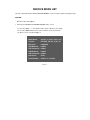
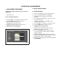
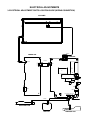
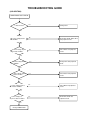
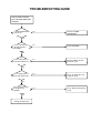
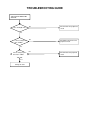
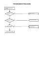
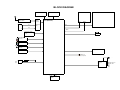
LT-22HG45E
SERVICE MANUAL
22" LED TV
ORIGINAL
MFR'S VERSION A
Design and specifications are subject to change without notice.
IMPORTANT SERVICE SAFETY INFORMATION
Operating the receiver outside of its cabinet or with its
back removed involves a shock hazard. Work on
these models should only be performed by those who
are thoroughly familiar with precautions necessary
when working on high voltage equipment.
Exercise care when servicing this chassis with power
applied. Many B plus and high voltage RF terminals are
exposed which, if carelessly contacted, can cause
serious shock or result in damage to the chassis.
Maintain interconnecting ground lead connections
between chassis, escutcheon, picture tube dag and
tuner cluster when operating the chassis.
These receivers have a "polarized" AC line cord. The AC
plug is designed to fit into standard AC outlets in one
direction only. The wide blade connects to the "ground
side" and the narrow blade connects to the "hot side" of
the AC line. This assures that the TV receiver is properly
grounded to the house wiring. If an extension cord must
be used, make sure it is of the "polarized" type.
Since the chassis of this receiver is connected to one
side of the AC supply during operation, service should
not be attempted by anyone not familiar with the
precautions necessary when working on these types
of equipment.
When it is necessary to make measurements or tests with
AC power applied to the receiver chassis, an Isolation
Transformer must be used as a safety precaution and to
prevent possible damage to transistors. The Isolation
Transformer should be connected between the TV line
cord plug and the AC power outlet.
When removing springs or spring mounted parts from the
tuner, tuner cluster or chassis, shatterproof goggles must
be worn. Keep others without shatterproof goggles away.
Before returning the receiver to the user, perform the
following safety checks:
1. Inspect all lead dress to make certain that leads are
not pinched or that hardware is not lodged between
the chassis and other metal parts in the receiver.
2. Replace all protective devices such as nonmetallic
control knobs, insulating fishpapers, cabinet backs,
adjustment and compartment covers or shields,
isolation resistor-capacitor networks, mechanical
insulators, etc.
3. To be sure that no shock hazard exists, a check for
the presence of leakage current should be made at
each exposed metal part having a return path to the
chassis (antenna, cabinet metal, screw heads,
knobs and/or shafts, escutcheon, etc.) in the
following manner.
Plug the AC line cord directly into a 120V AC receptacle.
(Do not use an Isolation Transformer during these
checks.) All checks must be repeated with the AC line
cord plug connection reversed. (If necessary, a
nonpolarized adapter plug must be used only for the
purpose of completing these checks.)
If available, measure current using an accurate leakage
current tester. Any reading of 0.35mA or more is
excessive and indicates a potential shock hazard which
must be corrected before returning the receiver to the
owner.
If a reliable leakage current tester is not available, this
alternate method of measurement should be used.
Using two clip leads, connect a 1500 ohm, 10 watt
resistor paralleled by a 0.15µF capacitor in series with
a known earth ground, such as a water pipe or conduit
and the metal part to be checked. Use a VTVM or
VOM with 1000 ohms per volt, or higher, sensitivity to
measure this AC voltage drop across the resistor. Any
reading of 0.35 volt RMS or more is excessive and
indicates a potential shock hazard which must be
corrected before returning the receiver to the owner.
VT VM
AC SCALE
0.15K OHMS
10W
TO EXPOSED
METAL PARTS
10µF
TEST PROBE
TO KNOWN
EARTH GROUND
ABOUT LEAD FREE SOLDER (PbF)
Distinction of PbF PCB:
PCBs (manufactured) using lead free solder will have a PbF printing on the PCB.
(Please refer to figures.)
Caution:
• Pb free solder has a higher melting point than standard solder;
Typically the melting point is 86oF~104oF(30oC~40oC) higher.
Please use a soldering iron with temperature control and adjust it to 650oF ± 20oF (350oC ± 10oC).
In case of using high temperature soldering iron, please be careful not to heat too long.
• Pb free solder will tend to splash when heated too high (about 1100oF/ 600oC).
• All products with the printed circuit board with PbF printing must be serviced with lead free solder.
When soldering or unsoldering, completely remove all of the solder from the pins or solder area,
and be sure to heat the soldering points with the lead free solder until it melts sufficiently.
Recommendations
Recommended lead free solder composition is Sn-3.0Ag-0.5Cu.
HOTEL MODE FUNCTION
To set the Hotel mode, please follow the steps below.
1.
2.
3.
4.
5.
6.
Press the MENU ---> 1147 button on the remote control.
Press the DOWN button on the remote control,
Select the "Setup" menu , then press ENTER button.
Select the "Hotel Mode" menu, Select "ON".
The Hotel mode setting menu will appear.
Using the UP/DOWN button on the remote control,
select the desired mode. Then press the ENTER button.
7. Using the LEFT/RIGHT button on the remote control,
set the mode to desired setting.
8. The Hotel mode has now been set up.
Hotel mode
Source Lock
Default Source
Channel Type
Default Program
Max Volume
Default Volume
Clone to USB
Restore from USB
On
Off
All
1
<>
>>
<>
<>
<>
100
50
>>
>>
To reset the Hotel mode, please follow the steps below.
1.
2.
3.
4.
5.
Press the MENU ---> 1147 button on the remote control.
Press the DOWN button on the remote control,
Select the "Setup" menu , then press ENTER button.
Select the "Hotel Mode" menu.
The setting items has now been returned to initial value.
Setting item
Setting value
Source Lock
ANTENNA/CABLE/AV
COMPONENT/SCART/
PC/HDMI/USB
Default Source
ANTENNA/CABLE/AV
COMPONENT/SCART/
PC/HDMI/USB
OFF
Channel Type
ANTENNA/CABLE/AV
COMPONENT/SCART/
PC/HDMI/USB
1
Setting of the CH if select "Default Source" to TV input.
Default Program
1~21
21
Setting of the CH if select "Default Source" to TV input.
Max volume
0~100
100
Setting of the maximum volume value.
Default Volume
0~50
50
Setting volume at Power on.
Clone to USB
Restore from USB
Initial value
FUNCTION
Setting Input skip, combine with "Default Source".
Setting Input Source, combine with "Source Lock"
If select "Source Lock" for this function disappear.
Setting of the Hotel Mode return factory setting.
Setting of the Password.
GENERAL SPECIFICATIONS
G-1
TV
System
LCD
LCD Size / Visual Size
LCD Type
Number of Pixels
Double Scan
View Range
Left/Right
Up/Down
Bright Dot
Zero Bright Dot Ratio
Color System
Speaker
Position
Size
Impedance
MAX
10%(Typical)
Sound Output
G-2
Tuning
System
NTSC3.58+4.43 /PAL60Hz
Broadcasting System
Tuner and
Receive CH
CH Coverage
Intermediate
Frequency
G-3
Power
Analog
Digital
System
Destination
Analog
Digital
Analog
Picture(FP)
Sound(FS)
FP-FS
Digital
Auto Tuning Method
Preset CH
Stereo/Dual TV Sound
Tuner Sound Muting
Power Source
AC
DC
Power Consumption
at AC
at DC
Stand by (at AC)
Protector
G-4
Regulation
G-5
Temperature
G-6
G-7
Operating Humidity
OSD Language
w/ EPG Timer
w/o EPG Timer
Per Year
Power Fuse
Safety
Radiation
X-Radiation
Operation
Storage
Space Around Unit
21.53 inch / 546.8mmV
Color TFT LCD
1920(H) x 1080(V)
No
85/85 degree
80/80 degree
n 3
70% above
PAL / SECAM
2 Speaker
Bottom
1.0 x 2.7 inch
8 ohm
2.0W + 2.0W
--Yes
PAL(B/G, D/K, I), SECAM(B/G, D/K)
DVB-T
DVB-T
1Tuner (Analog+Digital)
UK, I.R., CCIR Hyper+France CATV
45.75~858MHz
E2~E69
BG / II / DK
38.9 / 38.9 / 38.9MHz
33.4 / 32.9 / 32.4MHz
5.5 / 6.0 / 6.5MHz
DVB-T 36.167MHz
DVB-C
36.125MHz
ALL
Band
(Not C.C.I.R. CH Plan)
≦
4000 Service in total of Analog and Digital.
Nicam/A2 Dual
Yes
220-240V AC 50Hz
--31 W at AC 230 V 50 Hz
--0.49 W at AC 230 V 50 Hz
-kWh/Year
Yes
CE(EN60065:2002+AMD.11:2008)
CE
--o
o
+5 C ~ +40 C
o
o
-20 C ~ +60 C
100mm (4inch)
Less than 80% RH
English, Spanish, German, French, Italian, Swedish
Dutch, Russian, Portuguese, Turkish, Greek, Finnish
Hungarian, Polish, Danish, Norwegian, Czech, Slovak
G-8
Clock and
Timer
Sleep Timer
On/Off Timer
Timer Back-up (at Power Off Mode)
EPG Timer Events
Max Time
Step
Program(On Timer / Off Timer)
more than
120 Min
10 / 20 / 30 / 40 / 50 / 60 / 90 / 120 Min
1 Program / 1 Program
-Min
Sec
--
GENERAL SPECIFICATIONS
G-9
Remote
Control
Unit
Glow in Dark Remocon
Remocon Format
Format
Custom Code
Power Source
Total Keys
Keys
Voltage(D.C)
UM size x pcs
Power (Stand By)
Information
Audio /
1
2
3
4
5
6
7
8
9
0
Input Select
Guide(EPG)
Menu
Return
Enter / CH List
ⅠⅡ
↑
↓
←
→
T'TEXT Keys
Mute
Picture Size
Volume Up
Volume Down
TV
MEDIA
Freeze
Quick View
Play
Stop
Pause
Play Mode
Rec
T-Rec
Subtitle
CH Up / Page Up
CH Down / Page Down
Freeze / Hold
Quick View / Sub Page
Search- / Teletext
Play / Reveal
Search+ / F.T.B
Red/SkipGreen/Pause
Yellow/Stop
Cyan/Skip+
RC-TR
Yes
ORION
NEC
71-8E h
3V
UM-4 x 2 pcs
41
Keys
Yes
Yes
Yes
Yes
Yes
Yes
Yes
Yes
Yes
Yes
Yes
Yes
Yes
Yes
Yes
Yes
Yes
Yes
Yes
Yes
Yes
Yes
Yes
Yes
Yes
Yes
Yes
Yes
No
No
No
No
No
Yes
No
No
Yes
Yes
Yes
Yes
Yes
Yes
Yes
Yes
Yes
Yes
Yes
Yes
GENERAL SPECIFICATIONS
G-10 Features
Power On Memory
Auto Shut Off
Just Clock Function
Game Position
DNR
Yes
Yes
No
No
Comb Filter
Auto Set Up (Fast installation)
Picture Setting(TV)
Picture Setting(PC)
Audio
Language
Country
TV Location
Auto Power Off
E-POP Demo
Tuner Mode
Auto Tuning (Analog/DVB-T, DVB-C)
CH sort
ATS
Auto clock (Digital tuner)
Plug in start
Picture Mode
Brightness , Contrast , Color
Tint
Sharpness
DNR
Color Temperature
Backlight Control
MPEG NR
DBC (Dynamic Backlight Control)
Film Mode
Picture Mode
Brightness , Contrast , Color
HOR POSITION , VER POSITION
PHASE , CLOCK
AUTO ADJUST
RED , GREEN , BLUE
DNR
Color Temperature
Backlight
WXGA INPUT
WVGA INPUT
Sound Mode
Tone Control (Bass/Treble/Balance)
Surround
Equalizer
Speaker
Stable Sound
BBE
Yes
3D
Yes
3D
Yes
Yes
Yes
Yes
No
Yes
Yes
Yes
Yes
Yes
Yes
Yes
Yes
Yes
Yes
Yes
Yes
Yes
Yes
No
No
Yes
Yes
Yes
Yes
Yes
No
No
Yes
Yes
No
No
No
Yes
Yes
Yes
No
Yes
No
No
No
SRS WOW (SRS 3D/Focus/Tru Bass)
Tuning
Lock
Screen Saver
Variable Audio Out
Auto Tuning (Analog/Digital)
Manual Tuning (Analog/Digital)
Update Scan (Analog/Digital)
TV Connection
CH Skip (Analog/Digital)
CH Sort (Analog/Digital)
CH Edit (Analog/Digital)
Clean CH List (Analog/Digital)
Fine Tuning (Analog)
System Lock
Channel Lock
Parental Lock (Digital)
Hotel Lock
Inversion
Full White
Screen Saver
Static Image
Yes
Yes
No
Yes
Yes
Yes
Yes
Yes
Yes
Yes
Yes
Yes
Yes
No
No
Yes
No
GENERAL SPECIFICATIONS
T'Text
Text type
Text Language
Text and Picture
PVR
Timeshift
Timer Recording
EPG Recording
USB Media Player Photo
Music
Video
Container
Video Codec
Audio Codec
DivX DMF Support
Text
Internet
Hbb TV
BBC iPLAYER
Wide Mode (AUTO/4:3/16:9/Zoom1/Zoom2/1:1)
CH Label
Reset TV Setting
HD Zoom
Picture Scroll (Vertical Position)
PFC(Power Factor circuit)
Freeze frame
Plug and Play
Power Management
Hearing Impaired
Audio Description
Power On LED
HDMI Mode
PC Mode
Blue Back
Scart Spec
Scart1
AV in
AV out
S-Video in
RGB in
Scart2
AV in
AV out
S-Video in
RGB in
Digital Text (VBI teletext)
MHEG-5
MHP
EPG (BBC type 8Days Digital tuner only)
OAD (Over Air Download)
CI+
Common Interface (Digital tuner only)
Rec Screen Status
Ch sorting based on Ch List (Digital/Germany only)
Rename Carrier (Digital)
Edit Event Timer
Software Update via CI Slot
Preference Language (Audio/Subtitle/Digital Service)(Digital)
DVB Subtitle (Digital)
Clock
DST
Signal Status
Yes
Fastext / Toptext
English, German, Swedish, Finnish, Hungarian,
Italian, French, Portuguese, Spanish, Czech,
Slovak, Polish, Estonian, Lettish, Lithuanian,
Slovenian, Rumanian, Russian,
Ukrainian, Turkish, Greek, Hebrew, Farisi
Arabic, Danish, Flemish, Icelandic, Byelorussian
No
No
No
No
JPEG (.jpg/.jpeg), BMP (.bmp), PNG (.png)
WMA (.wma), WAVE (.wav), AAC-LC (.m4a)
HE-AAC (.m4a), MPEG1 (.mp2), MPEG4 (.m4a)
AVI (.avi), MKV (.mkv), MP4 (.mp4/,m4v),
PS (.mpg/.mpeg), TS (.ts/.tp/.trp), VOB (.vob)
Xvid, MPEG1, MPEG2, MPEG4 SP/ASP, H.264
MJPEG
MPEG1, MPEG2, MPEG4, AAC, AAC-LC
HE-AAC, PCM/ADPCM, AC3
No
Text (.txt)
No
No
Yes
Yes
Yes
Yes
No
No
Yes
No
Yes
Yes
Yes
No
Yes
Yes
Yes
Yes
Yes (A.Tuner/D.Tuner)
Yes
Yes
No
No
No
No
Yes
No
No
Yes
Yes
No
Yes
No
Yes
No
No
No
Yes
Yes
Yes
No
Yes
GENERAL SPECIFICATIONS
Digital Out
Decode(Down Mix)
Dolby Digital
Dolby Digital Plus
MPEG
HE AAC
Dolby Digital
Dolby Digital Plus
MPEG
HE AAC
PC Monitor Input
VGA (640x480)
VGA (720x400)
WVGA (848x480)
SVGA (800x600)
XGA (1024x768)
WXGA (1280x768)
WXGA (1280x720)
WXGA (1360x768)
SXGA (1280x1024)
WXGA+ (1440x900)
WSXGA+ (1680x1050)
FULL HD (1920x1080)
HDMI Input
VGA (640×480)
VGA (720x400)
WVGA (848x480)
SVGA (800x600)
XGA (1024x768)
WXGA (1280x768)
WXGA (1280x720)
WXGA (1360x768)
SXGA (1280x1024)
WXGA+ (1440x900)
WSXGA+ (1680x1050)
FULL HD (1920x1080)
720×480i (4:3)
720×480i (16:9)
720×480p (4:3)
720×480p (16:9)
720×576i (4:3)
720×576i (16:9)
720×576p (4:3)
720×576p (16:9)
1280×720p
1920×1080i
1920×1080p
CEC(ORION Standard)
Deep Color
xvYCC
Component Input
Wall Mount
Stand
720×480i (4:3)
720×480i (16:9)
720×480p (4:3)
720×480p (16:9)
720×576i (4:3)
720×576i (16:9)
720×576p (4:3)
720×576p (16:9)
1280×720p
1920×1080i
1920×1080p
Size W x H(mm)
Screw Size
Tilt
Swievel
Dolby Digital
Dolby Digital
PCM
PCM
Yes
Yes
Yes
Yes
Yes
Yes (60Hz)
No (Possible to Display)
No
Yes (60Hz)
Yes (60Hz)
Yes (60Hz)
Yes (60Hz)
Yes (60Hz)
Yes (60Hz)
Yes (60Hz)
No (Possible to Display)
Yes (60Hz)
Yes
Yes (60Hz)
No (Possible to Display)
No
Yes (60Hz)
Yes (60Hz)
Yes (60Hz)
Yes (60Hz)
Yes (60Hz)
Yes (60Hz)
Yes (60Hz)
No (Possible to Display)
Yes (60Hz)
Yes (60Hz)
Yes (60Hz)
Yes (60Hz)
Yes (60Hz)
Yes (50Hz)
Yes (50Hz)
Yes (50Hz)
Yes (50Hz)
Yes (50/60Hz)
Yes (50/60Hz)
Yes (24/50/60Hz)
No
No
No
Yes
Yes (60Hz)
Yes (60Hz)
Yes (60Hz)
Yes (60Hz)
Yes (50Hz)
Yes (50Hz)
Yes (50Hz)
Yes (50Hz)
Yes (50/60Hz)
Yes (50/60Hz)
No (Possible to Display)
Yes (75 x 75)
M4 x 10
No
No
GENERAL SPECIFICATIONS
G-11 Accessories
Owner's Manual
Language
w/Guarantee Card
Remote Control Unit
Rod Antenna
Poles
Terminal
Loop Antenna (W/ Antenna Change Plug)
Terminal
DVB-T Antenna
U/V Mixer
DC Car Cord (Center+)
Guarantee Card
Warning Sheet
Circuit Diagram
Antenna Change Plug
Service Facility List
Important Safeguard
Quick Set-up Sheet
Battery
UM size x pcs
OEM Brand
G-12 Interface
AC Adapter
AC Cord (for AC Adapter)
AC Cord
AV Cord (2Pin-1Pin)
HDMI-DVI Cable
3 in 1Mini Pin Cable (Y(CVBS)/Pb/Pr)
Registration Card
300 ohm to 75 ohm Antenna Adapter
Stand Screw
Stand
Frame Stand
Switch
Indicator
Power
System Select
Main Power SW
Channel Up / Menu Up
Channel Down / Menu Down
Volume Up / Menu >
Volume Down / Menu <
Menu
Play
Stop
Eject
Input Select/Enter
Power/Stand-by
On Timer
English/Czech/Slovak/Hungarian/Polish
Yes
Yes
No
No
No
No
No
No
No
No
No
No
No
Yes
Yes
UM-4 x 2 pcs
No
No
No
Yes
No
No
Yes
No
No
Yes (2pcs)
Yes
No
Yes
No
No
Yes
Yes
Yes
Yes
Yes
No
No
No
Yes
Yes (Blue / Red)
No
GENERAL SPECIFICATIONS
Terminals
Side
Rear
G-13 Set Size
Video Input 1
Audio Input 1
S- Input 1
Video Input 2
Audio Input 2
S- Input 2
Video Output
Audio Output
Digital Audio Out (Coaxial)
Euro Scart (21Pin)
Component In
Audio Input (Component In use)
HDMI Input 1
Audio Input (HDMI/DVI In use)
USB (Media)
Sub Woofer Output
Diversity
Ext Speaker
DC Jack 12V(Center +)
VHF/UHF Antenna Input
Headphone
CI Card Slot
AC Inlet
PC Monitor Input (D-Sub)
Audio Input
Euro Scart (21Pin)
Digital Audio Out (Coaxial)
VHF/UHF Antenna Input
PC Monitor Input (D-Sub)
Audio Input
Approx.
W x D x H (mm)
w/o Stand,Handle Approx. W x D x H (mm)
Net Approx.
Net w/o Stand,Handle Approx.
Gross Approx.
Gross w/Master Carton (Approx.)
G-14 Weight
G-15 Carton
Master Carton
Content
Material
Dimensions
W x D x H(mm)
Description of Origin
Gift Box
Material
Dimensions
W x D x H(mm)
Design
Description of Origin
Drop Test
G-16 Material
G-17 Environment
Mini Pin Jack(φ3.5) (CVBS Mini Pin Jack Alternative)
Composite Audio Input Alternative
Yes
PC Monitor Audio Input Alternative
Yes
No
No
No
No
No
Yes
Yes
Yes
No
No
Yes
No
DIN Type
Yes
Mini Pin Jack(φ3.5), STEREO
533.2 x 143.0 x 381.2
533.2 x 48.5 x 353.2
3.5kg
(7.7 lbs)
3.3kg
(7.3 lbs)
4.5kg
(9.9lbs)
--- kg
( --- lbs)
No
---Sets
-/--- x -- x -No
Yes
Single/White
620 x 129 x 452
As per Buyer's
No
Natural Dropping At 1 Corner / 3 Edges / 6 Surfaces
Height (cm)
Container Stuffing
w/Pallet
w/Wrapping
Cabinet
Mini Pin Jack(φ3.5)
RCA x 2(L, R)
No
No
No
No
No
No
Yes
No
Cabinet Front
Cabinet Rear
Stand
PCB
Non-Halogen
Eyelet
Environmental standard requirement
Pb- Free
Measures for Whisker
WEEE
80
1650
Sets/45' Trailer
Yes
Yes
PC+ABS 94V0 NON-HALOGEN
PS 94V0 NON-DECABROM
PC+ABS 94V0 NON-HALOGEN
No
Yes
Green procurement of JVC
Phase3(PHASE3A)
Yes
Yes
DISASSEMBLY INSTRUCTIONS
1. REMOVAL OF MECHANICAL PARTS
AND P.C. BOARDS
CAUTION
Be careful not to remove the LVDS cable forcibly, because
the LVDS cable may be damaged.
1-1: STAND ASS'Y (Refer to Fig. 1-1)
1-3: MAIN PCB (Refer to Fig. 1-3)
1. Disconnect the following connectors:
(CN2, CN3, CN5, CN6, CN11 and CN17).
2. Remove the screw (1).
3. Remove the 2 screws (2).
4. Remove the Plate Jack in the direction of arrow (A).
5. Remove the Shield Jack in the direction of arrow (B).
6. Remove the 4 screws (3).
7. Remove the Main Unit in the direction of arrow (C).
1. Remove the 3 screws (1).
2. Remove the Stand Ass'y in the direction of arrow.
(2)
(1)
(1)
Shield Jack
(2)
(1)
(1)
CN5
CN2
CN17
(A)
Stand Ass'y
(3)
(3)
CN6
(B)
Plate Jack
(3)
(3)
Main Unit
CN11
(C)
CN3
Fig. 1-1
Fig. 1-3
1-2: BACK CABI ASS'Y (Refer to Fig. 1-2)
1. Remove the screw (1).
2. Remove the 3 screws (2).
3. Remove the Back Cabi Ass'y in the direction of arrow.
1-4: POWER PCB (Refer to Fig. 1-4)
1. Disconnect the following connector: (CP7001).
2. Remove the 6 screws (1).
3. Remove the Power PCB in the direction of arrow.
(1)
(2)
(2)
(2)
(1)
(1)
(1)
(1)
CP7001
(1)
Power PCB
Fig. 1-4
Fig. 1-2
DISASSEMBLY INSTRUCTIONS
1-5: REMOCON PCB / LED PCB / OPERATION PCB
(Refer to Fig. 1-5)
1.
2.
3.
4.
5.
6.
Remove the Remocon PCB in the direction of arrow (A).
Remove the screw (1).
Remove the Angle Hinge in the direction of arrow (B).
Unlock the 2 supports (1).
Remove the LED PCB in the direction of arrow (C).
Remove the Operation PCB in the direction of arrow (D).
(1)
Angle Hing
Remocon PCB
(A)
(B)
LED PCB
Operation PCB
(C)
(2)
(D)
Fig. 1-5
DISASSEMBLY INSTRUCTIONS
2. REMOVAL AND INSTALLATION OF
FLAT PACKAGE IC
REMOVAL
1. Put Masking Tape (cotton tape) around the Flat Package
IC to protect other parts from any damage.
(Refer to Fig. 2-1.)
NOTE
3. When IC starts moving back and forth easily after
desoldering completely, pickup the corner of the IC using
tweezers and remove the IC by moving with the IC
desoldering machine. (Refer to Fig. 2-3.)
NOTE
Some ICs on the PCB are affixed with glue, so be
careful not to break or damage the foil of each IC
leads or solder lands under the IC when removing it.
Masking is carried out on all the parts located within
10 mm distance from IC leads.
Masking Tape
(Cotton Tape)
Blower type IC
desoldering machine
IC
Tweezers
Fig. 2-1
2. Heat the IC leads using a blower type IC desoldering
machine. (Refer to Fig. 2-2.)
IC
Fig. 2-3
NOTE
Do not rotate or move the IC back and forth , until IC
can move back and forth easily after desoldering the
leads completely.
Blower type IC
desoldering machine
4. Peel off the Masking Tape.
5. Absorb the solder left on the pattern using the Braided
Shield Wire. (Refer to Fig. 2-4.)
NOTE
Do not move the Braided Shield Wire in the vertical
direction towards the IC pattern.
Braided Shield Wire
Soldering Iron
IC
Fig. 2-2
IC pattern
Fig. 2-4
DISASSEMBLY INSTRUCTIONS
INSTALLATION
1. Take care of the polarity of new IC and then install the
new IC fitting on the printed circuit pattern. Then solder
each lead on the diagonal positions of IC temporarily.
(Refer to Fig. 2-5.)
4. When bridge-soldering between terminals and/or the
soldering amount are not enough, resolder using a
Thintip Soldering Iron. (Refer to Fig. 2-8.)
Thin-tip Soldering Iron
IC
Soldering Iron
Fig. 2-8
Solder temporarily
Solder temporarily
Fig. 2-5
5. Finally, confirm the soldering status on four sides of the
IC using a magnifying glass.
Confirm that no abnormality is found on the soldering
position and installation position of the parts around the
IC. If some abnormality is found, correct by resoldering.
NOTE
2. Supply the solder from the upper position of IC leads
sliding to the lower position of the IC leads.
(Refer to Fig. 2-6.)
Solder
Soldering Iron
IC
Supply soldering
from upper position
to lower position
Fig. 2-6
3. Absorb the solder left on the lead using the Braided
Shield Wire. (Refer to Fig. 2-7.)
NOTE
Do not absorb the solder to excess.
Soldering Iron
IC
Braided Shield Wire
Fig. 2-7
When the IC leads are bent during soldering and/or
repairing, do not repair the bending of leads. If the
bending of leads are repaired, the pattern may be
damaged. So, always be sure to replace the IC in this
case.
SERVICE MODE LIST
This unit is provided with the following SERVICE MODES so you can repair, examine and adjust easily.
CAUTION
Do not feel after other MENU.
1. Check of the SUM DATA and MICON VERSION on the screen.
1-1: Press the MENU ---> 1147 button on the remote control to select "Setup".
1-2: Press the DOWN button on the remote control to select "Version Info".
1-3: On the screen as shown in Fig. 1-1.
Model Name :
mt5365_eu_dvbs_cIplus_verf
Version :
IDTV0801_002114_8_001_70
OUl Code :
0x000C3B
H/W Model ID :
0x0D12
H/W Version ID : 0x0001
S/W Model ID :
0x0D12
S/W Version ID : 0x0001
Checksum :
C7C6
Serial Number :
2012-03-19 16:15:59
Fig. 1-1
ELECTRICAL ADJUSTMENTS
1. ADJUSTMENT PROCEDURE
2. BASIC ADJUSTMENTS
Prepare the following measurement tools for electrical
adjustments.
2-1: WHITE BALANCE
1.
2.
3.
1. Pattern Generator
On-Screen Display Adjustment
1. Press the MENU---> 1147 button on the remote control.
2. Press the DOWN button on the remote control.
3. Select the "Video" menu, then press
ENTER button on the remote control.
4. Select the "Color Temperature" menu , then press
ENTER button on the remote control.
5. On the screen as shown in Fig. 1-1.
Color Temperature
Cool
<>
R Gain
-37
G Gain
0
B Gain
102
R Offset
-2
G Offset
0
B Offset
-1
Fig 1-1
Place the set in Aging Test for more than 15 minutes.
Please select input About mode to adjust W/B.
Receive the gray scale pattern from the Pattern
Generator.
4. Press the INPUT SELECT button on the remote control
to set to the AV mode.
5. Using the remote control, set the brightness and
contrast to normal position.
6. Press the MENU---> 1147 button on the remote control.
7. Press the DOWN button on the remote control.
8. Select the "Video" menu, then press
ENTER button on the remote control.
9. Select the "Color Temperature" menu , then press
ENTER button on the remote control.
10. Press the UP/DOWN button on the remote control
to select the "R Gain", "G Gain", "B Gain", "R Offset",
"G Offset", "B Offset.
11. Adjust the LEFT/RIGHT button on the remote control
to whiten the R Gain, G Gain, B Gain, R Offset, G Offset,
B Offset at each step tone sections equally..
12. Perform the above adjustments 10 and 11 until the white
color is achieved.
ELECTRICAL ADJUSTMENTS
3. ELECTRICAL ADJUSTMENT PARTS LOCATION GUIDE (WIRING CONNECTION)
LCD PANEL
CD2801
POWER PCB
MAIN UNIT
CN11
CD3004
CP501
CP7001
CN7
CN3
T1
CN9
CN13
CN24
CN14
CN8
CN25
CN27
J502
CN23
CN26
CN6 CN5 CN2 CN17
CD805
SPEAKER
CP2204
OPERATION PCB
CD7602
OS7601 CP7601
LED PCB
REMOCON PCB
TROUBLESHOOTING GUIDE
(LCD SECTION)
POWER DOES NOT TURN ON
Is F501 broken?
Yes
Change F501.
No
Is there voltage C502
305VDC?
No
Check D507, D508, D518, D510
and peripheral circuit.
Yes
Is there voltage at pin6
of IC501 21VDC?
No
Check IC501 and peripheral
circuit.
Yes
Change R510 and peripheral
circuit.
Yes
Is there voltage Q501
169VDC?
Yes
Is there voltage at pin5
of IC501 21VDC?
Yes
Check IC501 and peripheral
circuit.
No
Check D505 and peripheral
circuit.
No
Check R516, R534 and
peripheral circuit.
Yes
Is there voltage at pin 8
of IC501 169VDC?
Yes
Is there voltage at
pin1 of IC501 5.7VDC?
Yes
Change POWER PCB.
TROUBLESHOOTING GUIDE
THE PICTURE APPEARS,
BUT THE AUDIO DOES NOT
APPEARS.
Is SP WIRE CONNECTOR
No
connected?
Connect SP WIRE
CONNECTOR.
Yes
Is there signal at wave
(SP.Lift) and wave
(SP.Right)?
Yes
Change SPEAKER.
No
Is there signal at pins 1
and 9 of IC YD1517(F)?
Yes
Check IC YD1517(F) and
peripheral circuit.
Yes
Is there signal at pins 4
and 6 of IC YD1517(F)?
Yes
Check IC YD1517(F) and
peripheral circuit.
Yes
Check D514 and peripheral
circuit.
Yes
Is there voltage at pin 7
of IC YD1517(F)
+12VDC?
Yes
Change IC YD1517(F).
TROUBLESHOOTING GUIDE
THE PICTURE DOES NOT
APPEAR
No
Does backlight shine?
Check IC7001 and peripheral
circuit.
Yes
No
Is there voltage at
pin2 12VDC?
Check D514 and L503 and
peripheral circuit.
Yes
Is there voltage at pin7
of IC 7001 5VDC?
Yes
Change IC 7001.
No
Check R7003 and peripheral
circuit.
TROUBLESHOOTING GUIDE
THE COLOR DOES NOT
APPEAR
Is Setting of color
Normal?
No
Adjust the color.
Yes
No
Is the color signal
received?
Receive the color signal.
Yes
No
Is there color signal at
IC MT5310CHHU?
Yes
Change IC MT5310CHHU.
Check IC MT5310CHHU and
peripheral circuit.
SEMICONDUCTOR BASE CONNECTIONS
DIODE
1N4006-A5
1SS133T-77
FCF10A20
SARS01
1F5
FCHS10A08
HZS12NB2
ZRM11C
HZS33NB2
RB056L-40TE25
S14K385E2S5M4
IC
ANODE
CATHODE
ANODE
BA36-PUR1DCB549T1/470
1
UDZSNP11B TE-17
MA111-(TX)
1
ATTINY48-MU
NR887D
TRANSISTOR
E
8
1
FA5640N-D1-TE1
1
2
B
3
KIA431A-AT
1
PS2561AL1-1-V(W)
C
KRC103SRTK
KTA1504S_Y_RTK
G
DS
FMV09N90E
BLOCK DIAGRAM
<Remonon PCB>
DVB-T/C TUNER
TDTK-G941D
PCMCIA
<Operation PCB>
<LCD PANEL>
<DVD PCB>
MPEG/SCALER
DEMOD.
BUS SW
TS
MT5310 (MEDIATEK)
Y/C
SPDIF
LVDS
MT5135AE
(MTK)
Bus
SPDIF
SPI FLASH 64Mbit
EN25Q64-104HIP
(EON)
【HDMI-1】
【AV2/Comp A-in】
AUDIO L/R
【AV2/Component】
CVBS/Y,
Pb, Pr
Mini
【PC/Comp
Audio IN】
AUDIO L/R
【SCART1】
CVBS_In/Out
RGB
Audio_In/Out
D-sub 【PC】
15pin RGB
Side
SCART
SPDIF Out
(Coaxial) Side
HP Jack
5V
USB
FUSE
USB
Side
Sound AMP
YD1517P
(YD)
DDR3-1333 1Gb
NT5CB64M16DP-CF
(NANYA)
Main Speaker
2W + 2W
PRINTED CIRCUIT BOARDS
POWER (INSERTED PARTS)
D505
IC505
R512
CP501
IC502
C516
C512
R518
L504
C7010
C522
W845
C7001
0
C5
L7002
7
HS503
C514
D514
R511_1
W007
F501
CEL788A
IC7001
D513
10
R5
C542_1
R503
C524
SH503
SH507
J502_1
CP7001
POWER (CHIP MOUNTED PARTS)
C7013
B7002
R528
R520
R506
IC501
C509
R523
R519
C523 C521
R515
R525
R513
R524
W807
R516
C505
C503
C501
W852
Q503
Q504
R526
R504
R514
Q502
R522
R529
R532
C536
CEL788A
D517
W806
C7017
C517
R7004
C7011_2
C7005
C7004
R7002 C7002
R7001 R7003
C7012
R7017
R7013
R7014
C7016
D7003
C7015
SOLDER SIDE
R7010
R7011
R7012
R7005 R7008
R7009
W001
W003
D516
T501_1
C520
Q501
C513
W803
W823
D527
B7001
W004
C511
HS502
W812
W847
W802
L503
C502
HS501
D511
R502
R505
R534
D528
W009
D518
L501_1
W008
D523
R507
D508
D506
D507
W814
C506
D504_1
FIRE OF RISK
.MARKED AS REPLACE -
C508
C504
R501
D510
D512
TH501
C527
W810
34
C5
SH505
SH502
SOLDER SIDE
PRINTED CIRCUIT BOARDS
POWER (INSERTED PARTS)
SOLDER SIDE
POWER (CHIP MOUNTED PARTS)
SOLDER SIDE
PRINTED CIRCUIT BOARDS
REMOCON (INSERTED PARTS)
SOLDER SIDE
SOLDER SIDE
D7602_1
LED (INSERTED PARTS)
CEJ570A
CEJ572A
CP7601
OS7601
CD7602
LED (CHIP MOUNTED PARTS)
REMOCON (CHIP MOUNTED PARTS)
SOLDER SIDE
SOLDER SIDE
CEJ572A
B2201
B2202
CEK600A
B2203
2
C2203
17
R2267 R2268
D2204
9
C2231
C2232
R2274_1
R2279
R2284
C2225
R2271
R2272
R2273_1
C2202 C2201
R2283
R2281
R2282
R2280
R2278
OPE
25
R2266_1
1
R2264
IC2204
C2229
C2230
R2265_1
R2269
C2228
C2227
C2226
OPERATION (TOP SIDE)
B2204
CP2204
C7602
CEJ570A
R7605
W803
W804
W801
PRINTED CIRCUIT BOARDS
LED (INSERTED PARTS)
REMOCON (INSERTED PARTS)
SOLDER SIDE
SOLDER SIDE
LED (CHIP MOUNTED PARTS)
REMOCON (CHIP MOUNTED PARTS)
SOLDER SIDE
SOLDER SIDE
OPERATION (TOP SIDE)
A
B
C
D
E
F
G
H
POWER SCHEMATIC DIAGRAM
SH507
YQ-12
(POWER PCB)
SH503
YQ-12
W810
W812
C514
E
C507
250V
0.001 E
250V 0.001 E
C534
12M1W
RCR
W847
TH501
W823
ZRM11C
C502
J502_1
CCT2302-0721C
SOUND+B
25V 1000 ZLJ
D505
C522
7
50V 0.047
B
C523
10K 1/16W
CAUTION:
IS THE LIVE CONNECTION
4
GND
5
GND
6
SW+12V/GND
7
SW+12V
8
A
REF
3
2
1
B
AT+5.8V
AT+12V
SOUND+B
P.FAIL_SW
Q504
KRC103SRTK3.3
0
0
0
SOUND_GND
NC.
LIGHT_CTL
NC.
5.8
2.5
SEC
POWER FAIL SW
Q502
KTA1504S_Y_RTK
2.2K 1/16W
+-1%
R523
C
0
3
GND
GND
5.8
R525
11.0
AT+5.8V
P.FAIL_SW
Q503
KRC103SRTK
2.2K 1/16W
+-1%
R515
2
2
10K 1/16W
5.8
1K 1/16W
11.0
1
AT+5.8V
5.8
REGULATOR IC
KIA431A-AT
IC502
1
2
4
3
FEED BACK IC
IC505
PS2561AL1-1-V(W)
12.0
50V 0.001
C536
B
R519
AT+5.8V
R529
C527
C521
PRI
SOUND+B
9
SOUND+B
10
SOUND_GND
11
SOUND_GND
12
3
POWER_ON_H 13
POWER_FAIL
14
LIGHT_CTL
15
INVERTER_H
16
2
0
4A 125V
:FOR CONTINUED PROTECTION AGAINST FIRE HAZARD,
REPLACE ONLY WITH THE SAME TYPE FUSE
4A 250V (F501)
2.5A 250V (F501)
, 4A 250V (F502)
, 2.5A 250V (F502)
AND 4A 125V (F503)
AND 4A 125V (F503)
4A 250V (F501)
2.5A 250V (F501)
, 4A 250V (F502)
, 2.5A 250V (F502)
ET 4A 125V (F503)
ET 4A 125V (F503)
UNE PROTECTION CONTINUE LES RISQUES D’INCEIE
ATTENTION :POUR
N’UTILISER QUE DES FUSIBLE DE MEME TYPE
IS MANUFACTURED BY SKYGATE CO.,LTD., TYPE SCT.
CAUTION :F501
:F502 IS MANUFACTURED BY SKYGATE CO.,LTD., TYPE SCT.
:F503 IS MANUFACTURED BY SKYGATE CO.,LTD., TYPE 20N.
A
W802
C512
8
FROM/TO MAIN UNIT
0.001
5
R524
220 1/16W
FOR Q501
HS501
763WAAA120
1/16W
+-1%
R513
W807
CP501
(CN3)
00_6216_016_000_808+
10K 1/16W
3
0
1
C517
D517
UDZSNP11B
R532
D516
1SS133
R522
R518
100 1/4W
POWER_FAIL
2.2K 1/10W
11
2.8
CAUTION
25V 220 YXF_P
C504
50V 4.7 YXF
15 1/4W
12
910
B
50V 0.1
1F5
8128042Z
1
50V 470P CH
2.5A 250V
AT+5.8V
10uH
TSL0808
10V 1000
W845
1F5
D506
100 1/4W
R507
C509
R534
C520
21.3
D511
6
4A 250V
50V 0.001 B
ZLH
2
1
L504
3
OUT
50V 22 YXF 2.5mm
GND
FOR D523
HS502
763WAAA120
T501_1
C516
8
VCC
NC
21.0
50V 10P CH
IS
7
NC
6
1
FB
GND
4
C505
100K 1/16W
IC PIN
C503
R516
50V 0.015 B
50V 330P CH
C501
3
D512
HZS12NB2
0
VH
5
1.8
ZCD
2
2.8
3
W852
4
R502
330 1/4W
5.7
5
D523
FCHS10A08
0.27 1W
4
LED+12V
10uH
TSL0808
C511
C524
HZS33NB2
R505
POWER CONTROL IC
IC501
FA5640N-D1-TE1
169.0
SOUND_GND
L503
FOR D514
HS503
763WAAA198
SARS01
D513
(SOUND GND)
25V 470 ZLH
C542_1
220K 1W RCR
R511_1
C513
2KV 330P R
HZS33NB2
D528
630V 0.022 ECWF(L)
33K 1/16W
D527
AT+12V
B
5.6K 1/2W
W803
SWITCHING
Q501
FMV09N90E D 169.0
G
20.0
S 1.8
33 1/16W
R506
R501
5
5.6K 1/2W
R514
R512
1N4006-A5
0.001
2
6
3
2.5A 250V
D514
FCF10A20
2
ZRM11C
SH505
YQ-12
1
D507
1W
D518
R510
D510
ZRM11C
0.22
D508
ZRM11C
400V 82 GJ
4
310V 0.1 LE-MX
3
LINE FILTER
L501_1
JLB24123
C508
LE-MX
C506
2
310V 0.22
D504_1
S14K385E2S5M4
R520
R504
330K 1/8W 330K 1/8W
(32-16)
(32-16)
330K
1/8W
(32-16)
1
7
GND
USA:4A(T)250V/EU:2.5A(T)250V
4A 250V
LED+12V
SOUND_GND
LIGHT_CTL
1
6
R528
F501
SCT_2.5A250V
FROM/TO BACKLIGHT INVERTER
B57153S0479A001
330K
1/8W
(32-16)
R526
7
8
FRAMGND3
W814
R503
FRAMEGND1
250V 470P
8
SH502
YQ-12
B
PCB240
CEL788
NOTE: THIS SCHEMATIC DIAGRAM IS THE LATEST AT THE TIME
OF PRINTING AND SUBJECT TO CHANGE WITHOUT NOTICE
NOTE: THE RESISTOR MARKED F IS FUSE RESISTOR.
THE ALUMI ELECTROLYTIC CAPACITOR MARKED NP
IS NON POLAR ONE.
NOTE:THE DC VOLTAGE AT EACH PART WAS MEASURED
WITH THE DIGITAL TESTER WHEN THE COLOR BROADCAST
WAS RECEIVED IN GOOD CONDITION AND PICTURE IS NORMAL.
C
D
E
THESE PARTS MARKED BY
PIECES REPAREES PAR UN
ETANT
ATTENTION:LES
CAUTION:SINCE
CRITICAL FOR SAFETY,USE ONES
DANGEREUSES AN POINT DE VUE SECURITE
N’UTILISER QUE CELLS DECRITES
DANS LA NOMENCLATURE DES PIECES
F
ARE
CAUTION: DIGITAL TRANSISTOR
DESCRIBED IN PARTS LIST ONLY
G
H
1
A
B
C
D
E
F
G
H
BACKLIGHT INVERTER SCHEMATIC DIAGRAM
(POWER PCB)
8
8
7
7
PATTERN
FROM/TO LED PCB
C7016
50V 470P CH
D7003
L7002
B7002
10V 960mA
HCB3216KF-391T20
22uH PF13
RB056L-40
CP7001
(CD2003)
00_6232_007_006_800+
VFB
0.8V
C7004
R7003
0.001 B
C7013
6
VLED
5
ILED1
4
ILED2
ILED2
3
ILED2
1
2
6
50V
25V 0.47 B
960mA
7
VLED
R7005
10K 1/16W
+-1%
50V 0.0015
B
4.8
R7017
FB
NC
47K 1/16W
C7010
GND
C7017
NC
50V 0.01 B
SW
W806
10 1/16W
C7011_2
R7014
0
47 1/10W
47 1/10W
R7013
C7015
B7001
SOUND_GND
W4BRH3.5X6X1.0
50V 0.0022 B
C7001
16V 100 ML
5.0
5.0
25V 100 ZLG
C7012
LIGHT_CTL
8
EN
7
VIN
6
12.7
0
5
1
SS
50V 0.1 B 100 1/10W
LED+12V
R7008
3.9 1/4W +-1%
R7009
3.9 1/4W +-1%
R7010
3.9
5
1/4W +-1%
R7011
GNDPATTERN
R7001
1/4W +-1%
R7012
50V 0.1 B
R7002
1K 1/16W
C7002
3.9
22K 1/16W
5
BS
50V 0.1 B 1608
6
5.0
2
FROM/TO POWER
R7004
3
C7005
4
INVERTER DRIVE
IC7001
NR887D
VLED
3.9
1/4W +-1%
GND
4
4
3
3
2
2
PCB240
CEL788
NOTE: THIS SCHEMATIC DIAGRAM IS THE LATEST AT THE TIME
OF PRINTING AND SUBJECT TO CHANGE WITHOUT NOTICE
1
A
B
C
D
NOTE:THE DC VOLTAGE AT EACH PART WAS MEASURED
WITH THE DIGITAL TESTER WHEN THE COLOR BROADCAST
WAS RECEIVED IN GOOD CONDITION AND PICTURE IS NORMAL.
E
1
F
G
H
A
B
C
D
E
F
G
H
HEAD PHONE/REMOCON/LED SCHEMATIC DIAGRAM
(REMOCON/LED PCB)
8
8
(HEAD PHONE/REMOCON PCB)
7
7
OS7601
KSM-603LM2M(OR)
R7605
Vout 1
GND 2
B+ 3
100 1/16W
1608
C7602
6.3V 4.7
B
1608
W801
6
6
FROM/TO MAIN UNIT
(CN6) CP7601
A2001WV-3A
5
AT+3.3V
1
GND
2
REMOCON IN
CD7601_2
E8232206
5
3
PCBDA0
CEJ570
(LED PCB)
4
4
FROM/TO MAIN UNIT
CD7602
E8231204
POWER ON LED 1
(CN2)
W804
W803
2
R
B
1
3
3
GND
2
STAND_BY LED
3
3
ST-BY/POWER
D7602_1
BA36-PUR1DCB549T1/470
PCBDT0
CEJ572
2
2
NOTE: THIS SCHEMATIC DIAGRAM IS THE LATEST AT THE TIME
OF PRINTING AND SUBJECT TO CHANGE WITHOUT NOTICE
NOTE:THE DC VOLTAGE AT EACH PART WAS MEASURED
WITH THE DIGITAL TESTER WHEN THE COLOR BROADCAST
WAS RECEIVED IN GOOD CONDITION AND PICTURE IS NORMAL.
1
A
B
C
D
E
1
F
G
H
A
B
C
D
E
F
G
H
OPERATION SCHEMATIC DIAGRAM
(OPERATION PCB)
8
8
7
7
OUT3
B
C2228
25V 0.022
B
C2229
25V 0.022
B
C2230
25V 0.022
B
C2231
25V 0.022
B
R2278
1K 1/16W
C2232
25V 0.022 B
R2279
1K 1/16W
12
OUT4
B
25V 0.022
3.28
R2280
1K 1/16W
3.36
R2281
1K 1/16W
3.28
R2282
1K 1/16W
3.28
R2283
1K 1/16W
3.28
R2284
1K 1/16W
32
330 1/16W
10K 1/16W +-1%
25V 0.022
C2227
0 3.28 NC0 3.28
3.28 3.36 3.36
1
3
4
5
6
7
8
2
PD3 PD4 PA2 VCC GND PA3 PB6 PB7
PD2
PD5
31
R2264
R2265_1
C2226
13
IC
PD1
KEY_B
4
GND
FCM1608KF-102T02
B2203
FCM1608KF-102T02
B2204
FCM1608KF-102T02
NC
R2266_1
C2202
25V 0.01
B
C2203
25V 0.01
B
18K 1/16W +-1%
R2267
33K 1/16W
C2225
10V 0.1 B
10K 1/16W
3.36
D2204
MA111
JG2225
NC 0
JG2226
R2269
8.2K 1/16W
NC 0
OUT8
3.36
OUT7 0
NC
5
R2271
3.9K 1/16W
OUT6
R2272
560 1/16W
OUT5
R2273_1
5.6K 1/16W +-1%
OUT2
R2274_1
22K 1/16W +-1%
OUT1
10
IC2204
ATTINY48-MU
PD7
11
PC6
KEY_SENSOR_IC
PB0
PC5
PB1
PC4
PB2
PC3
PB3
PC2
PB4
PC1 PC0 PA1 GND PC7 PA0 AVCC PB5
24
23
22
21
20
19
18
17
3.36 3.36 3.36
0
0 3.36 3.36 3.28
NC
14
3
B2202
R2268
PD0
15
KEY_A
B
10
16
2
6.3V
30
AT+3.3V
FCM1608KF-102T02
29
1
B2201
28
CD805
CH243303
C2201
NC
PD6
27
CP2204 (CN6)
A2001WR-S04-T
3.28
26
3.28
FROM/TO MAIN UNIT
25
3.36
9
3.28
6
3.28
6
JG2205 KEY6/MENU
0 NC
3.28
JG2207 KEY8/VOL+
JG2208 KEY1/CH+
JG2209 KEY2/INPUT
JG2210 KEY3/VOLJG2211 KEY4/POWER
5
JG2212 KEY5/CH-
JG2227 MOSI
JG2228 MISO
JG2229 SCK
JG2230 RST
4
4
JG2231 VCC
JG2232 GND
3
3
2
2
PCB270
CEK600
NOTE: THIS SCHEMATIC DIAGRAM IS THE LATEST AT THE TIME
OF PRINTING AND SUBJECT TO CHANGE WITHOUT NOTICE
1
A
B
C
NOTE:THE DC VOLTAGE AT EACH PART WAS MEASURED
WITH THE DIGITAL TESTER WHEN THE COLOR BROADCAST
WAS RECEIVED IN GOOD CONDITION AND PICTURE IS NORMAL.
D
E
F
1
G
H
A
B
C
D
E
F
G
H
INTERCONNECTION DIAGRAM
8
8
CD2003
CP7001
VLED
1
1
7
7
VLED
VLED
2
2
6
6
VLED
VLED
3
3
5
5
VLED
N1
4
4
4
4
ILED1
N2
5
5
3
3
N2
6
6
2
2
ILED2
ILED2
N2
7
7
1
1
ILED2
CP501
LED PCB
PCBFM0
CEL789
7
NC.
NC.
CN3
AT+5.8V
1
1
1
1
AT+5.8V
2
2
2
2
AT+5.8V
3
3
3
3
GND
4
4
4
4
GND
5
5
5
5
GND
6
6
6
6
SW+12V/GND
7
7
7
7
SW+12V
8
8
8
8
SOUND+B
9
9
9
9
SOUND+B
10
10
10
10
SOUND_GND
11
11
11
11
SOUND_GND
12
12
12
12
POWER_ON_H 13
13
13
13
POWER_FAIL
14
14
14
14
LIGHT_CTL
15
15
15
15
INVERTER_H
16
16
16
16
CN11
1
2
3
4
5
CN4
1
2
13
7
14
8
4
15
9
16
10
17
11
1
18
12
2
2
12
6
3
19
13
3
20
14
4
1
11
5
2
22
16
6
23
17
24
18
CN23
1
25
19
2
20
3
21
4
22
5
23
6
24
6
21
15
5
POWER PCB
PCB240
CEL788
10
4
1
7
9
3
CN17
6
8
2
3
J3801
7
1
CN12
230V AC 50Hz
CD501
6
CN10
26
27
28
29
30
7
5
8
1
AT+3.3V
1
1
1
1
KEY_A
2
2
2
2
KEY_B
3
3
3
3
4
GND
4
4
4
4
5
2
J4208
3
19
6
18
7
17
8
16
9
15
10
14
11
12
13
GND
2
2
2
2
3
3
3
3
REMOCON IN
15
16
17
18
7
3 B+
14
11
CN6
1
10
1
9
2 GND
1
8
1 Vout
1
19
6
REMOCON PCB
PCBDA0
CEJ570
5
20
21
2
3
4
COMMAND TRANSMITTER
TM101
CP7601
AT+3.3V
4
12
13
4
OS7601
5
CN13
CN5
21
NC
OPERATION PCB
PCB270
CEK600
CP2204
20
NC
3
2
R
B
1
3
1
3
ST-BY/POWER
D7602_1
CD7602
POWER ON LED
1
GND
2
STAND_BY LED
3
1
CN2
1
2
2
2
3
3
3
1
LED PCB
PCBDT0
CEJ572
2
2
MAIN UNIT
MAIN001
1
NOTE:THE DC VOLTAGE AT EACH PART WAS MEASURED
WITH THE DIGITAL TESTER WHEN THE COLOR BROADCAST
WAS RECEIVED IN GOOD CONDITION AND PICTURE IS NORMAL.
A
B
C
THESE PARTS MARKED BY
CAUTION:SINCE
CRITICAL FOR SAFETY,USE ONES
PIECES REPAREES PAR UN
ETANT
ATTENTION:LES
DANGEREUSES AN POINT DE VUE SECURITE
ARE
DESCRIBED IN PARTS LIST ONLY
D
1
N’UTILISER QUE CELLS DECRITES
DANS LA NOMENCLATURE DES PIECES
E
F
G
H
WAVEFORMS
SCALER VIDEO/AUDIO
20µs/div
500mV/div
AV IN
10µs/div
200mV/div
PY
10µs/div
100mV/div
PR
10µs/div
200mV/div
PB
1ms/div
200mV/div
AU AUDIO IN L
1ms/div
200mV/div
AU AUDIO IN R
2ms/div
200mV/div
PC AUDIO L
2ms/div
200mV/div
PC AUDIO R
1ms/div
500mV/div
AUDIO OUT L
1ms/div
500mV/div
AUDIO OUT R
1ms/div
2V/div
SPEAKER L
1ms/div
2V/div
SPEAKER R
NOTE : Main Board Signal Input/Output.
MECHANICAL EXPLODED VIEW
113
112
103B
206 207
110
110
114
103B
205
205
205
110
103B
103A
103B
111
103
102B
102B
102A
102
PCBDA0
(REMOCON PCB ASS'Y)
204
205
MAIN001
(MAIN UNIT)
203
204
201
203
203
203
203
101C
203
202
108
PCB240
(POWER PCB ASS'Y)
202
106
101B
101D
203
202
201
203
105
PCBDT0
(LED PCB ASS'Y)
101D
109
101D
PCB270
(OPERATION PCB ASS'Y)
101D
101
107
101D
101A
115
101D
104
MECHANICAL EXPLODED VIEW
(PACKING DIAGRAM)
11
3
2
4
1
8
6, 12, 13, 14, 15
7
9
10
5
MECHANICAL REPLACEMENT PARTS LIST
REF. NO.
PART NO.
DESCRIPTION
QUANTITY
FRONT CABI ASS'Y
CABINET FRONT
FRONT PLATE
GUIDE REMOCON
FELT SHEET
1
1
1
1
6
101
101A
101B
101C
101D
X-7A708A911A
X-708WPDA718
X-711WPAA316
X-713WPD0028
X-800WQ00181
102A
102B
X-702WPAC014 CABINET BACK
X-800WQ0A312 FELT SHEET
1
2
103
103A
103B
X-7A704A375A STAND ASS'Y
X-704WPA0161 STAND
X-800SRA0002 CUSHION LEG
1
1
4
104
105
106
107
108
109
X-7290000210
X-709WPA0051
X-752WUAA016
X-759WNAA043
X-761WPAA430
X-761WSAA217
DOUBLE FACE TAPE
HOLDER WIRE
SHIELD JACK
SHEET PC
PLATE JACK
ANGLE HINGE
1
1
1
1
1
1
110
111
112
113
114
115
X-769WSA0022
X-704WPA0162
X-722538A287
X-723000F825
X-723000F826
X-800WQ0A266
VESA SHAFT
STAND FRAME
SHEET RATING
SHEET JACK 1
SHEET JACK 2
FELT SHEET
4
1
1
1
1
1
201
202
203
204
205
206
207
X-8110K2660U
X-8109I30A0U
X-810722660U
X-810722680U
X-8109230A0S
X-8107K2660S
X-810722680S
SCREW TAP TITE(P) LAMI HEAD
SCREW TAP TITE(B) WH7
SCREW TAP TITE(S) BIND
SCREW,TAP TITE(S) BIND
SCREW TAP TITE(B) BIND
SCREW TAP TITE(S) LAMI HEAD
SCREW TAP TITE(S) BIND
VEB1349-A
2.6x6
3x10
2.6x6
M2.6x8
3x10
2.6x6
M2.6x8
2
3
10
2
6
1
1
ACCESSORY REPLACEMENT PARTS LIST
REF. NO.
PART NO.
DESCRIPTION
1
2
3
4
5
6
7
8
9
X-120A155811
X-06EYB18003
X-076R0TR021
X-791WHA0173
X-723000F778
X-723000F779
X-791WHAA322
X-792PHAA067
X-792PHAA068
CORD SET AC
CORD,RCA PIN
TRANSMITTER
FILM BAG
SHEET CARTON
ENERGY LABEL
FILM BAG
PACKAGE TOP
PACKAGE BOTTOM
10
11
12
13
14
15
X-793PCDA452
X-795PCA0001
X-8905000013
X-JB5PD000
X-J3LJ0307A
X-J3LJ0351A
GIFT BOX
SHEET PROTECTION
SCREW
POLYBAG INSTRUCTION(RED CAUTION)
QUICK SET UP SHEET
INSTRUCTION BOOK(EN/CZ/SK/HU/PL)
QUANTITY
O27-007BK
06.03.02.0176
R56-2294
1
1
1
1
1
1
1
1
1
1
1
1
1
1
1
ELECTRICAL REPLACEMENT PARTS LIST
REF. NO.
PART NO.
DESCRIPTION
QUANTITY
REMOCON PCB ASS'Y
*** PCB ***
PCBDA0 X-A3LJ03WDA0P REMOCON PCB ASS'Y
CEJ570A
1
HPWGJ101T50
1
GRM188B30J475KE18D
1
*** RESISTORS ***
R7605
X-R803R9101J
RC
100 OHM 1/16W
*** CAPACITORS ***
C7602
X-CS0PB0PQ6K CC
4.7 UF 6.3V B
*** OTHERS ***
CP7601
X-06GG230029
CONNECTOR PCB SIDE
A2001WV-3A
1
OS7601
X-077Q038012
REMOTE RECEIVER
KSM-603LM2M(OR)
1
CEJ572A
1
BA36-PUR1DCB549T1/470
1
E8231204
1
M215HGE-P02-LED OR7A
1
CEL788A
1
CR1/2W-SS562JT/B
BCS4J0331A10
RCR60CT52A126J
1206W8J0334T5E
ERX1FJR27H
HPWG J 333 T50
BCS4J0101A10
RF1CL15AR22J
RCR60CT52A224J
CR1/2W-SS562JT/B
HPWGJ221T50
HPWG J 330 T50
HPWGJ102T50
HPWGJ104T50
BCS4J0101A10
1
1
1
1
1
1
1
1
1
1
1
1
1
1
1
LED PCB ASS'Y
*** PCB ***
PCBDT0 X-A3LJ03WDT0P LED PCB ASS'Y
*** DIODES ***
D7602
X-0021991050
LED
*** OTHERS ***
CD7602
X-06E8231204
CORD CONNECTOR
*** OTHERS ***
! V7201
X-A3LJ03WFM0P LED MODULE ASS'Y
POWER PCB ASS'Y
*** PCB ***
PCB240
X-A3LJ03W240P POWER PCB ASS'Y
*** RESISTORS ***
!
!
!
!
!
!
!
R501
R502
R503
R504
R505
R506
R507
R510
R511
R512
R513
R514
R515
R516
R518
X-R002T2562J
X-R002T4331J
X-RC31X1126J
X-R8X2R8334J
X-R3K781R27J
X-R803R9333J
X-R002T4101J
X-R63881R22J
X-RC31X1224J
X-R002T2562J
X-R803R9221J
X-R803R9330J
X-R803R9102J
X-R803R9104J
X-R002T4101J
RC
5.6K OHM 1/2W
RC
330 OHM 1/4W
RC
12M OHM 1W
RC
330K OHM 1/8W
R,METAL OXIDE 0.27 OHM 1W
RC
33K OHM 1/16W
RC
100 OHM 1/4W
R,FUSE
0.22 OHM 1W
RC
220K OHM 1W
RC
5.6K OHM 1/2W
RC
220 OHM 1/16W
RC
33 OHM 1/16W
RC
1K OHM 1/16W
RC
100K OHM 1/16W
RC
100 OHM 1/4W
ELECTRICAL REPLACEMENT PARTS LIST
R519
! R520
R522
R523
R524
R525
! R526
! R528
R529
R532
R534
R7001
R7002
R7003
R7004
R7005
R7008
R7009
R7010
R7011
R7012
R7013
R7014
R7017
X-R803R9103J
X-R8X2R8334J
X-R801R7222J
X-R803R9222F
X-R803R9911F
X-R803R9222F
X-R8X2R8334J
X-R8X2R8334J
X-R803R9103J
X-R803R9103J
X-R002T4150J
X-R803R9102J
X-R803R9223J
X-R803R9100J
X-R801R7101J
X-R803R9103F
X-R861R43R9F
X-R861R43R9F
X-R861R43R9F
X-R861R43R9F
X-R861R43R9F
X-R801R7470J
X-R801R7470J
X-R803R9473J
RC
RC
RC
RC
RC
RC
RC
RC
RC
RC
RC
RC
RC
RC
RC
RC
RC
RC
R
R
RC
RC
RC
RC
10K OHM 1/16W
330K OHM 1/8W
2.2K OHM 1/10W
2.2K OHM 1/16W
910 OHM 1/16W
2.2K OHM 1/16W
330K OHM 1/8W
330K OHM 1/8W
10K OHM 1/16W
10K OHM 1/16W
15 OHM 1/4W
1K OHM 1/16W
22K OHM 1/16W
10 OHM 1/16W
100 OHM 1/10W
10K OHM 1/16W
3.9 OHM 1/4W
3.9 OHM 1/4W
3.9 OHM 1/4W
3.9 OHM 1/4W
3.9 OHM 1/4W
47 OHM 1/10W
47 OHM 1/10W
47K OHM 1/16W
HPWGJ103T50
1206W8J0334T5E
HMWAJ0222T50
HPWGF222T50
HPWGF911T50
HPWGF222T50
1206W8J0334T5E
1206W8J0334T5E
HPWGJ103T50
HPWGJ103T50
BCS4J0150A10
HPWGJ102T50
HPWG J 223 T50
HPWGJ100T50
HMWAJ0101T50
HPWGF103T50
MCR10EZHFL3R9
MCR10EZHFL3R9
MCR10EZHFL3R9
MCR10EZHFL3R9
MCR10EZHFL3R9
HMWAJ0470T50
HMWAJ0470T50
HPWG J 473 T50
1
1
1
1
1
1
1
1
1
1
1
1
1
1
1
1
1
1
1
1
1
1
1
1
C0603X7R153K500NT
LGJ2G820MELB
C0603C0G331J500NT
10ZLH1000MEFC10*12.5
GRM1882C1H100JA01D
LE224-MX-C3.5
DE1E3KX102MB4BL01
LE104-MX-C3.5
C0603X7R104K500NT
25ZLH470MEFCT8 10*12.5
25YXF220MEFCTA 8*11.5
DEHR33D331KB3B
DE1B3KX471KB4BL01
50YXF22MEFCT1 5*11
C0603X7R102K500NT
50YXF4.7MEFCT1 5*11
GRM188B11H473KA01D
25VZLJ1000MKC10*20
C0603CG471J500NT
UP025B102K-A-BZ
UP025B102K-A-BZ
DE1E3KX102MB4BL01
C0603X7R102K500NT
ECWF6223JLB
16ML101MEFCT5 6.3*7
C0603X7R104K500NT
C0603X7R152K500NT
C0603X7R104K500NT
25ZLG100MEFC6.3*11
UP050B104K-A-BZ
GRM188B31E474KA75D
C0603X7R102K500NT
C0603X7R222K500NT
C0603CG471J500NT
C0603X7R103K500NT
1
1
1
1
1
1
1
1
1
1
1
1
1
1
1
1
1
1
1
1
1
1
1
1
1
1
1
1
1
1
1
1
1
1
1
*** CAPACITORS ***
!
!
!
!
!
!
!
!
!
!
!
!
!
!
!
C501
C502
C503
C504
C505
C506
C507
C508
C509
C511
C512
C513
C514
C516
C517
C520
C521
C522
C523
C524
C527
C534
C536
C542
C7001
C7002
C7004
C7005
C7010
C7011
C7012
C7013
C7015
C7016
C7017
X-CS0PB04E4K
X-E83FHH820D
X-CS0PCH4L2J
X-E8E101102M
X-CS0PCH411D
X-P4K12D224K
X-CE39E0M13M
X-P4K12D104K
X-CS0PB0415K
X-E8E1T3471M
X-E8E2T3221D
X-C03L0R7L2K
X-CE39E0MQ2K
X-E8E2U5220D
X-CS0PB0413K
X-E8E2U54R7D
X-CS0PB04Q4K
X-E9E8F3102D
X-CS0PCH4Q2J
X-CRGTB0413K
X-CRGTB0413K
X-CE39E0M13M
X-CS0PB0413K
X-P416F5223J
X-E9EGU2101M
X-CS0PB0415K
X-CS0PB04E3K
X-CS0PB0415K
X-E8EMU3101D
X-CQGTB0415K
X-CS0PB03Q5K
X-CS0PB0413K
X-CS0PB04H3K
X-CS0PCH4Q2J
X-CS0PB0414K
CC
CE
CC
CE
CC
CMPP
CC
CMPP
CC
CE
CE
CC
CC
CE
CC
CE
CC
CE
CC
CC
CC
CC
CC
CMPP
CE
CC
CC
CC
CE
CC
CC
CC
CC
CC
CC
0.015 UF 50V B
82 UF 400V
330 PF 50V CH
1000 UF 10V
10 PF 50V CH
0.22 UF 310V
0.001 UF 250V E
0.1 UF 310V
0.1 UF 50V B
470 UF 25V
220 UF 25V
330 PF 2KV R
470 PF 250V E
22 UF 50V
0.001 UF 50V B
4.7 UF 50V
0.047 UF 50V B
1000 UF 25V
470 PF 50V CH
0.001 UF 50V B
0.001 UF 50V B
0.001 UF 250V E
0.001 UF 50V B
0.022 UF 630V ECWF(L)
100 UF 16V
0.1 UF 50V B
0.0015UF 50V B
0.1 UF 50V B
100 UF 25V
0.1 UF 50V B
0.47 UF 25V B
0.001 UF 50V B
0.0022UF 50V B
470 PF 50V CH
0.01 UF 50V B
ELECTRICAL REPLACEMENT PARTS LIST
*** DIODES ***
! D504
! D505
D506
! D507
! D508
! D510
! D511
D512
! D513
! D514
! D516
D517
! D518
! D523
! D527
! D528
D7003
X-D7KZ385E20
X-D4CTN40060
X-D4JX001F50
X-D4JXRM11C0
X-D4JXRM11C0
X-D4JXRM11C0
X-D4JX001F50
X-DJBUA12012
X-D4JXARS010
X-D28A10A200
X-D1VT001330
X-DE7RB1102B
X-D4JXRM11C0
X-D28A10A080
X-DJBUA33012
X-DJBUA33012
X-D27RB056L0
DIODE VARISTA
DIODE SILICON
DIODE SILICON
DIODE SILICON
DIODE SILICON
DIODE SILICON
DIODE SILICON
DIODE ZENER
DIODE SILICON
DIODE SILICON
DIODE,SILICON
DIODE ZENER
DIODE SILICON
DIODE SCHOTTKY BARRIER
DIODE ZENER
DIODE ZENER
DIODE SCHOTTKY
S14K385E2S5M4
1N4006-A5
1F5
ZRM11C
ZRM11C
ZRM11C
1F5
HZS12NB2
SARS01
FCF10A20
1SS133T-77
UDZSNP11B TE-17
ZRM11C
FCHS10A08
HZS33NB2
HZS33NB2
RB056L-40TE25
1
1
1
1
1
1
1
1
1
1
1
1
1
1
1
1
1
FA5640N-D1-TE1
KIA431A-AT
PS2561AL1-1-V(W)
NR887D
1
1
1
1
FMV09N90E
KTA1504S_Y_RTK
KRC103SRTK
KRC103SRTK
1
1
1
1
*** ICS ***
! IC501
! IC502
! IC505
IC7001
X-ICAJ056400
X-I1KJ9A431A
X-000220002W
X-ILYD0887D0
POWER IC CONTROL
VARIABLE SHUNT REGULATOR TAPE
PHOTO COUPLER
LED DRIVER IC
*** TRANSISTORS ***
! Q501
Q502
Q503
Q504
X-TK1009N900
X-TAAA1504SY
X-TNAAC05002
X-TNAAC05002
FET
TRANSISTOR SILICON
COMPOUND TRANSISTOR
COMPOUND TRANSISTOR
*** COILS ***
B7001
B7002
X-024HT03564
X-024HC13914
CORE,BEADS
CORE,BEADS
W4BRH3.5X6X1.0
HCB3216KF-391T20
1
1
! L501
L503
L504
L7002
X-029B000187
X-02167E100K
X-02167E100K
X-021D0N220M
COIL,LINE FILTER
COIL
10 UH
COI
10 UH
COIL
22 UH
JLB24123
TSL0808RA-100K2R
TSL0808RA-100K2R
PF13-220-OS
1
1
1
1
8128042Z
1
CCT2302-0721C
1
00_6216_016_000_808+
00_6232_007_006_800+
1
1
SCT 2.5A
1
B57153S0479A001
1
*** TRANSFORMERS ***
! T501
X-048128042Z
TRANSFORMER,SWITCHING
*** JACKS ***
! J502
X-064Q2A0004
JACK,AC
*** CONNECTORS ***
CP501
CP7001
X-069E7G0630
X-069EV73030
CONNECTOR PCB SIDE
CONNECTOR PCB SIDE
*** FUSES ***
! F501
X-0805T02501
FUSE
*** THERMISTOR ***
! TH501
X-DSVD8E4R7M THERMISTOR
ELECTRICAL REPLACEMENT PARTS LIST
*** OTHERS ***
EL2401
EL2402
X-124116281A
X-124120301A
EYE LET
EYE LET
EYE LET XRY16X28BD
EYE LET XRY20X30BD
9
2
SH502
SH503
SH505
SH507
X-126D000045
X-126D000045
X-126D000045
X-126D000045
TERMINAL PIN
TERMINAL PIN
TERMINAL PIN
TERMINAL PIN
YQ-12
YQ-12
YQ-12
YQ-12
1
1
1
1
CEK600A
1
0402WGJ0331TCE
0402WGF0103TCE
0402WGF1802TCE
0402WGJ0333TCE
0402WGJ0103TCE
0402WGJ0822TCE
0402WGJ0392TCE
0402WGJ0561TCE
0402WGF5601TCE
0402WGF2202TCE
0402WGJ0102TCE
0402WGJ0102TCE
0402WGJ0102TCE
0402WGJ0102TCE
0402WGJ0102TCE
0402WGJ0102TCE
0402WGJ0102TCE
1
1
1
1
1
1
1
1
1
1
1
1
1
1
1
1
1
GRM188B30J106ME69D+A01
GRM155B11E103KA01D
GRM155B11E103KA01D
C0402X5R104K100NY
C0402X7R223K250NY
C0402X7R223K250NY
C0402X7R223K250NY
C0402X7R223K250NY
C0402X7R223K250NY
C0402X7R223K250NY
C0402X7R223K250NY
1
1
1
1
1
1
1
1
1
1
1
MA111-(TX)
1
ATTINY48-MU
1
OPERATION PCB ASS'Y
*** PCB ***
PCB270
X-A3LJ03W270P OPERATION PCB ASS'Y
*** RESISTORS ***
R2264
R2265
R2266
R2267
R2268
R2269
R2271
R2272
R2273
R2274
R2278
R2279
R2280
R2281
R2282
R2283
R2284
X-R808R9331J
X-R808R9103F
X-R808R9183F
X-R808R9333J
X-R808R9103J
X-R808R9822J
X-R808R9392J
X-R808R9561J
X-R808R9562F
X-R808R9223F
X-R808R9102J
X-R808R9102J
X-R808R9102J
X-R808R9102J
X-R808R9102J
X-R808R9102J
X-R808R9102J
RC
RC
RC
RC
RC
RC
RC
RC
RC
RC
RC
RC
RC
RC
RC
RC
RC
330 OHM 1/16W
10K OHM 1/16W
18K OHM 1/16W
33K OHM 1/16W
10K OHM 1/16W
8.2K OHM 1/16W
3.9K OHM 1/16W
560 OHM 1/16W
5.6K OHM 1/16W
22K OHM 1/16W
1K OHM 1/16W
1K OHM 1/16W
1K OHM 1/16W
1K OHM 1/16W
1K OHM 1/16W
1K OHM 1/16W
1K OHM 1/16W
*** CAPACITORS ***
C2201
C2202
C2203
C2225
C2226
C2227
C2228
C2229
C2230
C2231
C2232
X-CS0PB0P17M
X-CS0UB0314K
X-CS0UB0314K
X-CS0UB0N15K
X-CS0UB03H4K
X-CS0UB03H4K
X-CS0UB03H4K
X-CS0UB03H4K
X-CS0UB03H4K
X-CS0UB03H4K
X-CS0UB03H4K
CC
CC
CC
CC
CC
CC
CC
CC
CC
CC
CC
10 UF 6.3V B
0.01 UF 25V B
0.01 UF 25V B
0.1 UF 10V B
0.022 UF 25V B
0.022 UF 25V B
0.022 UF 25V B
0.022 UF 25V B
0.022 UF 25V B
0.022 UF 25V B
0.022 UF 25V B
*** DIODES ***
D2204
X-DGERMA1110 DIODE SILICON
*** ICS ***
IC2204
X-IG6N0AT480
MCU 8BIT W/4K FLASH Q-TOUCH
ELECTRICAL REPLACEMENT PARTS LIST
*** COILS ***
B2201
B2202
B2203
B2204
X-024HC51023
X-024HC51023
X-024HC51023
X-024HC51023
CORE,BEADS
CORE,BEADS
CORE,BEADS
CORE,BEADS
FCM1608KF-102T02FCM1608KF-102T02
FCM1608KF-102T02
FCM1608KF-102T02
FCM1608KF-102T02
1
1
1
1
A2001WR-S04-T
1
CH242503
E8242501
2H0G0501
1
1
1
TDTK-G731D(A)
1
*** OTHERS ***
CP2204
X-06GG240059
CONNECTOR PCB SIDE
AND OTHERS
*** CONNECTORS ***
CD805
CD805
CD3004
X-06CH242503
X-06E8242501
X-122H0G0501
CORD CONNECTOR
CORD CONNECTOR
CORD JUMPER
*** TUNER ***
TU001
X-0164E03021
DIGITAL TUNER
*** OTHERS ***
BT001
BT002
X-141U004021
X-141U004021
BATTERY,MANGAN
BATTERY,MANGAN
AAA(R03)
AAA(R03)
1
1
CD2801
CD7601
X-06EH2U1011
X-06E8232206
CORD CONNECTOR
CORD CONNECTOR
EH2U1011
E8232206
1
1
MAIN001
X-1564Y00005
MAIN UNIT
T.MT5310.91A
1
SP301
X-070Y433020
SPEAKER
S0307F08-F
1
RESISTOR
CARBON RESISTOR
RC……………………
CAPACITORS
CERAMIC CAPACITOR
CC……………………
ALUMI ELECTROLYTIC CAPACITOR
CE……………………
POLYESTER CAPACITOR
CP……………………
POLYPROPYLENE CAPACITOR
CPP………………….
PLASTIC CAPACITOR
CPL………………….
METAL POLYESTER CAPACITOR
CMP………………….
METAL PLASTIC CAPACITOR
CMPL………………..
METAL POLYPROPYLENE CAPACITOR
CMPP……………….
SPEC.NO.
M3LJ-03W
O/R NO.
F233167