1
UVI51 USER’S MANUAL (v 5.0)
Alfredo del Río
Dpto. de Tecnología Electrónica
ETSII-Universidad de Vigo
36200 VIGO
Spain (Europe)
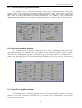
Note: A Spanish version of UVI51, software and manual, is available in the site
http://www.dte.uvigo.es .
Contents
1. Introduction
2. UVI51 operation modes
3. Installing UVI51. What is new in version 5.0?
4. The Assistant: UVI51
4.1 Multi-micro mode
4.2 Single-micro mode
5. The Assembler: UVIENS51
5.1
5.2
5.3
5.4
Introduction
Running the assembler
Assembly language syntax
Assembler restrictions
6. The Simulator: UVISIM51
6.1
6.2
6.3
6.4
6.5
6.6
6.7
6.8
Main window and basic topics
Source file window
Timers window
Interrupts window
Serial port window
Use of colors
Editing values
What 8051 hardware configuration is simulated?
7. UVI51 Logic Analyzer
7.1 Introduction
7.2 Description
7.3 Finding patterns in the chronograms
Appendix A1: CNX files syntax
A1.1 Defining microcontrollers
A1.2 Defining external peripherals
Appendix A2: Customizing UVI51
Appendix A3: Technical support
0
UVI-51 User’s Manual (v5.0)
1. Introduction
UVI51 is the 8051 microcontroller teaching/learning environment developed in the
University of Vigo (Spain), Dpto. de Tecnología Electrónica.
The present manual is delivered with the free distribution version (UVI51 v5.0). This
version limits the size of source files to 500 lines. In the commercial version this limit is extended
to 3000 lines.
The environment includes a set of programs and auxiliary files. The main program is the
UVI51 assistant. The assistant guides the user through the software development and verification
processes. The assembler UVIENS51 generates the executable code. The simulator UVISIM51
helps in program verification. These programs are specifically designed to work together.
However, the user can configure the system to use other commercial assemblers (see appendix A2
for details).
The next sections show a brief description of the various elements included in UVI51.
This manual is not intended as a guide to 8051 microcontrollers. Furthermore, a basic
knowledge of this family of microcontrollers is needed to follow some parts of the manual.
However, UVI51 includes a set of source files that can be used as examples, or even as a short
course on the 8051.
2. UVI51 operation modes
UVI51 can operate in two different modes called single-micro and multi-micro.
The single-micro mode is the fastest and simplest to use. However, in this mode only one
microcontroller can be simulated and no external peripherals can be defined.
The multi-micro mode is much more powerful than the single-micro. The user can define a
system consisting of up to four microcontrollers plus a set of external peripherals as pushbuttons,
switches, LEDs, displays and a logic analyzer. The system is specified by a system configuration
file (with the CNX extension).
In multi-micro mode the following parameters can be defined for each micro in the system:
&
&
&
Clock frequency.
Program memory (ROM) size.
External RAM memory (XRAM) size.
Appendix A1 includes a detailed description of configuration files syntax.
3. Installing UVI51. What is new in version 5.0?
This software is supplied as a packed file named UVI51_50.ZIP. This ZIP file must be
unpacked previously to installation procedure.
1
UVI-51 User’s Manual (v5.0)
This UVI51 version is a free distribution software. However, it must be distributed as a
whole and no part must be modified.
All the programs in UVI51 are MSDOS applications and do not require any special
installation. The set of files resulting of the unpacking process must be copied into a subdirectory.
The creation of a subdirectory for work files (system definition files, source files, etc) is
suggested, but not a must.
Execution under Microsoft Windows’95 and later versions
The best way to start UVI51 under Windows is to create a shortcut to UVI51.EXE (the
UVI51 assistant). The suggested shortcut properties are:
PROGRAM- Close at exit; Change icon- UVI51.ICO
SCREEN- Full screen
MISCELLANEOUS- Do not use screen saver. Low inactive sensitivity
New in version 5.0
&
&
&
&
&
&
&
&
&
New simulator’s graphical interface including windows and buttons.
The simulator enables continuous program execution while showing and updating the source
code or the embedded peripherals windows. The user is allowed to edit values on these
windows.
A symbol table format has been added to the simulator’s RAM window.
Simulator’s source window can be synchronized or desynchronized with the execution process.
A Find utility, for searching text in the source window, has been added.
The simulation speed can be adapted to user’s requirements.
The external peripheral display present in older versions has been changed to a graphical one.
The new display indicates the nodes each peripheral is connected to.
New external peripherals have been added. Moreover, the old syntax of CNX files has been
extended to include peripheral labels. Appendix A1 describes this syntax.
The new assembler version includes a more powerful set of directives.
4. The Assistant: UVI51
The following command lines can be used to run the assistant from DOS prompt. The same
lines can be used to define the shortcut under Windows.
UVI51 or UVI51 file.cnx
UVI51 file.src
2
UVI-51 User’s Manual (v5.0)
The options on first line configure UVI51 to operate in multi-micro mode (see section 2).
The first one starts the assistant with the NONAME.CNX system configuration file, while the
second uses the file indicated in the command line. File extension must be CNX.
The second line configures UVI51 to operate in single-micro mode. This mode does not use
any configuration file. The file indicated in the command line is considered as the source file for
the only microcontroller to be simulated. File extension must be SRC. The microcontroller is
configured to run at 12 MHz clock frequency (1 µs machine cycle) with a 4096 bytes ROM and a
2048 bytes XRAM.
Once the assistant has started in one mode, its operation mode can not be changed to the
other. The only way to change the operation mode is to start the assistant again with the suitable
DOS command line (or Windows shortcut).
4.1. Multi-micro mode
When operating in multi-micro mode, the assistant screen shows the following buttons:
[HELP] This button is used to open the help file HELP.TXT. This file contains information about
the 8051. Users can edit the file according to their needs.
[OPEN] This button is used to open an already existing configuration file (CNX). This file will
guide the operation of the assistant.
[NEW] This button is used to open a new configuration file (CNX). The user must edit the file to
define the system before the system can be simulated (see the next button).
[file.CNX] This button shows the name of the active CNX file. It is used to edit this file.
[SIMULATE] This button is active only if the microcontroller(s) program(s) has (have) been
successfully assembled. It is used to start the execution of the simulator UVISIM51.
[ANALYZE] This button is used to run the logic analyzer viewer. It is active only if a logic
analyzer has been defined in the configuration file and a simulation has been successfully carried
out (see appendix A1). The viewer shows the chronograms of all the nodes in the system.
[EXIT] This button is used to quit the assistant and to return to the operating system.
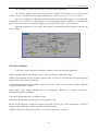
In addition, a table of buttons is shown with the format:
SOURCES
ASSEMBLER
OUTPUT
[file1.SRC]
[--A->]
[file1.LST]
[file2.SRC]
[--A->]
[file2.LST]
The buttons in the left column are used to edit the source files in assembly language. The
buttons in the central column call the assembler on the corresponding source file. Finally, the
buttons in the right column are used to edit the list files generated by the assembler. Each row
corresponds to the program of one microcontroller.
While a file has not been successfully assembled, the associated LST file button is shown
in gray. Even so, the LST file can be edited using the button in order to check for errors in the
assembly process.
3
UVI-51 User’s Manual (v5.0)
The following line is shown in the bottom of the screen:
STATUS MESSAGES:
The assembler, or other utilities, show their console messages under this line.
The same area is also used when creating a new CNX file with the [NEW] button, to write
the new file name.
4.2. Single-micro mode
When operating in single-micro mode, the assistant shows a screen similar to that of the
multi-micro mode (see section 4.1). A brief description of the differences follows:
[OPEN] This button is used to open an existing source file (SRC).
[NEW] This button is used to create a new source file (SRC).
[SIMULATE] If the source file has been successfully assembled, this button calls the simulator.
The table of buttons contains, in this mode, a single line corresponding to the only
microcontroller in the system, and is functionally equivalent to the one in multi-micro mode.
SOURCE
[file1.SRC]
ASSEMBLER
[--A->]
OUTPUT
[file1.LST]
5. The Assembler: UVIENS51
This section describes the features and use of UVIENS51 the assembler supplied with
UVI51.
5.1. Introduction
UVIENS51 is a ‘mini-assembler’ for the 8051 family of microcontrollers. It has been
developed as a part of UVI51. This assembler is very easy to use and its syntax is very similar to
that of other commercial assemblers like Intel’s ASM51. UVIENS51 generates absolute code, and
there is no need for a separate linker. Macroinstructions are not supported.
5.2. Running the assembler
From the assistant, click the [--A->] button to run the assembler. UVIENS51 is an MSDOS
application, therefore it can be also called from the MSDOS command line:
UVIENS51 file.src
file.src being the name of the source code file to be assembled. A path can be included in the file
name.
4
UVI-51 User’s Manual (v5.0)
The assembler creates an output file with the same name as the source file but with LST
extension. If no error is found, another file with HEX extension is created containing the absolute
code in Intel-Hex format.
The LST file is useful to check for errors the assembler can eventually find. Moreover, the
simulator needs this file to correlate source code to object code.
5.3. Assembly language syntax
The source file must be an ASCII file. Since UVIENS51 generates absolute code, it does
not accept some directives commonly supported by other assemblers. A list of valid directives and
formats follows:
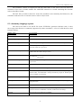
DIRECTIVE
FUNCTION
ORG expression
Updates program counter to the value of expression
symbol EQU expression
Defines a symbol of type number with the value of expression
symbol BIT expression
Defines a symbol of type bit address with the value of expression
symbol DATA expression
Defines a symbol of type direct byte address (direct internal RAM)
with the value of expression
symbol IDATA expression
Defines a symbol of type indirect byte address (indirect internal
RAM) with the value of expression
symbol XDATA expression
Defines a symbol of type external byte address (external RAM) with
the value of expression
symbol CODE expression
Defines a symbol of type code address (ROM) with the value of
expression
DB expression
Generates a byte of code with the value of expression
DB 'char'
Generates a byte of code using the ASCII code of char.
DB "string"
Generates a byte of code for every character in the string using their
ASCII codes. The backslash \ must precede any single or double quote
to be included in the string.
DB ‘a’, 25 , "string"
Generates bytes of code for all the elements in the list.
DW expression
Generates 2 bytes of code with the value of expression, the upper byte
being the first.
END
Indicates the end of file (optional)
#IF expression
If expression evaluates to 0, the following lines are not assembled
until the directive #ENDIF is found (conditional assembly).
#ENDIF
Restores the unconditional assembly.
5
UVI-51 User’s Manual (v5.0)
All the expressions must be absolute and computable at the first assembly pass (only
backward references are permitted). The only exception are forward references to labels when
using the EQU directive and, of course, jump and call instructions.
The instruction syntax is similar to that used by many commercial assemblers. Some
examples follow:
label:
<label:> mnemonic parameter_list ;optional comment
<label:> mnemonic ;optional comment
<label:> ;optional comment
;comment line without instruction
The valid mnemonics are those defined by Intel for the 8051 family. If two or more
parameters are used in one instruction, they must be separated by commas. Numeric parameters
can be replaced by evaluable expressions. All the expressions are evaluated into numbers in the
range 0000h to 0FFFFh. The evaluation takes place from left to right without precedence levels.
Therefore, brackets must be used to define the desired precedence. The following operators are
supported:
+
Add
-
Subtract and change sign unary operator
*
Unsigned multiplication
/
Quotient of whole division
%
Remainder of whole division
&
Logic AND
|
Logic OR
~
Logic NOT, equivalent to 1’s complement
^
Exclusive OR
<
Shift left one bit position
>
Shift right one bit position
[
Most significant byte of operand (similar to Intel’s HIGH)
]
Least significant byte of operand (similar to Intel’s LOW)
The evaluation is performed using 16-bit values. Negative values are represented in 2’s
complement notation. Result type is assigned according to the following rules:
&
&
The same type as the operand in unary operators.
When adding or subtracting, if one operator is a generic number and the other is not, the
result is of the type of the non numeric operator.
6
UVI-51 User’s Manual (v5.0)
&
Generic number –as if it were defined using the EQU directive- in other case.
When using jump or call instructions, the parameter must be an absolute address –usually
in the form of a label-, never a relative distance. The assembler computes the relative jump if
necessary.
The special symbol $ can be used to refer to the current value of the program counter.
Therefore, SJMP $ indicates a dead loop. If a DB directive generates several bytes, the symbol $
stands for the address where the first byte will be located.
The generic JMP and CALL mnemonics are recognized by the assembler. The shortest
valid jump –or call- is selected by the assembler in backward references. In forward references,
the assembler selects always the long type, i. e. LJMP or LCALL.
The assembler converts the source code into uppercase. There are only two exceptions:
•
Comments
•
Characters between single or double quotes
5.4. Assembler restrictions
The following limits apply to the present assembler version:
&
&
&
&
&
The maximum number of symbols is 1000. These include the symbols defined in the
UVI51.REG file.
The size of the source file is limited to the amount of free conventional memory available for
DOS applications. As a rule of thumb, the maximum number of lines is about 10000.
Lines of source code are truncated to 80 characters.
Symbols and labels are truncated to 31 characters.
Parameter lists are truncated to 31 characters in both instructions and directives. This should
be in mind particularly when using long DB directives.
7
UVI-51 User’s Manual (v5.0)
6. The Simulator UVISIM51
This section describes the features and use of UVISIM51, the simulator supplied with
UVI51.
6.1. Main window and basic topics
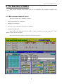
The main features of UVISIM51 v5.0 are:
&
&
&
&
Single and multimicro simulation.
Graphic user interface.
Step over, trace into and continuous run options.
Unlimited breakpoints.
Both mouse and keyboard can be used to control simulator operation. However, some
options require the use of mouse.
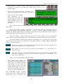
The simulator main window is shown in the following figure.
8
UVI-51 User’s Manual (v5.0)
The upper window, in orange –brown in some monitors- is called the system window. Its
header shows the name of the system configuration file. Under the header there is a set of buttons
related to system operation. Under these buttons, the external peripherals are drawn in a set of
cells (see appendix A1 for details). A brief description of the system window buttons follows:
This button is used to quit the simulator. It is equivalent to Shift+Esc keys.
This button is used to show a brief help. It is equivalent to F1 key.
This button is used to reset all the micros in the system, clear the contents of their
RAMs, reset the global time clock and clear all the breakpoints. It is equivalent to
'C' (uppercase) key.
This button is used to reset all the micros in the system. It is equivalent to 'R'
(uppercase) key.
This button is used to run the simulator or to stop it. It is equivalent to 's'
(lowercase) key.
In addition to a user command, any of the following conditions stop the simulator:
•
•
•
The program counter is pointing to a non initialized ROM address. In this case, a real micro
should go into an undetermined state.
A breakpoint is reached.
The reserved A5h code is found.
This button is used to reset the global time clock. This button is inhibited if a logic
analyzer has been defined in the CNX file, in order to avoid duplicity in time stamps.
Select the microcontroller whose information is displayed in the
microcontroller window (see below). There are as many buttons as micros
have been defined in the system. As an exception, when only one
microcontroller has been defined, no button of this kind is shown.
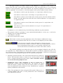
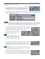
The external peripheral area shows the state of every peripheral defined in the CNX file.
(see appendix A1). Node numbers are shown either in black -to indicate a high level state- or in
red –low level state-. Node numbers are replaced by labels –node names- if they have been defined
in the CNX file. Each peripheral type has its own characteristic picture.
•
Manually operated switches. The switch name and electrical symbol are
shown. The moveable contact is shown in its current position. Switch
state is changed clicking the little button. Node controlled switches
are not shown in the peripheral area.
•
Pushbuttons (keys). This peripheral is new in version 5.0. A
pushbutton is shown with its assigned name. The contacts are closed
while the button is pushed. Since only one mouse pointer is available,
only one pushbutton can be pushed at a time. Should this be a problem,
replace pushbuttons with switches.
•
LEDs. This peripheral is shown using the LED symbol. When active, it
is shown lighting. The color is red by default but can be defined for
each LED in the CNX file.
9
UVI-51 User’s Manual (v5.0)
•
Hex displays -7 segments style- with multiplexing capability. Active
segments are shown in red. When the -enable node is set to '1' no
segment lights.
•
LCD Screen with serial link, controlled via 3
signals. See appendix A1, section A1.2 for details.
•
LCD Screen with parallel
link
(standard).
It
is
functionally equivalent to
Trident MDLS 16265 and
other standard screens. See
appendix A1, section A1.2
for details.
The CNX file defines the actual position where every external peripheral is shown, within
this window.
The system window includes a simulation speed indicator. The units are Instructions Per
Second. The speed can be modified using the ‘+’ and ‘-‘ buttons. When maximum speed is
selected, the indicator shows MAX. The numeric value is shown in red when the requested speed is
greater than the maximum possible for the computer.
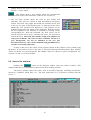
The lower window, in blue, is called microcontroller window. There is a set of subwindows
inside it, each one showing information on some different element of the selected microcontroller.
The microcontroller window header indicates the number -0 to 3- of the micro in the system
and the name of its source file. Furthermore, the header includes 3 buttons and an elapsed time
indicator. These buttons are:
This button is used to reset the selected microcontroller and to clear the contents of its
RAM. It is equivalent to 'c' (lowercase) key.
This button is used to reset the selected microcontroller. It is equivalent to 'r'
(lowercase) key.
This button is used to execute one instruction tracing into subroutines. If pushed while
shift key is pressed, it executes one instruction stepping over subroutines. It is
equivalent to Enter key.
There is a set of subwindows under the header.
•
The RAM window shows the
contents of the internal RAM as a
table. The arrows button switches
between the 128 lower and 128
upper –indirect- bytes. It is worth
noting that the upper 128 bytes do
not exist in the basic 8051 micro.
Values are show in hexadecimal.
The RAM/SMB button switches
between the table format described
above and a list of symbols. The
10
UVI-51 User’s Manual (v5.0)
PgUp and PgDn keys can be used to
scroll the list.
•
The XRAM window shows the contents of 16 consecutive
addresses of the external RAM. The arrow buttons are used to
scroll the table. In order to reach quickly any XRAM address,
the displayed pointer –over blue background- can be edited.
•
The Program window shows the contents of program memory. Code addresses are shown in
the first column while code itself is shown in the second. The corresponding source file lines
are shown preceded by a line number.
This button is used to open a new window, called Source window, that shows the source
code in more detail, including the lines that do not generate code, as those containing
only comments or some directives. The button is equivalent to the 'F' (uppercase) key.
Section 6.2 describes the operations that can be performed in the source window.
•
The CPU window shows the contents of some registers associated
to the central process unit. The contents of some interesting
XRAM and ROM addresses are also shown. The values of some
registers are shown both in hexadecimal and binary codes.
•
The Timer/Counter window shows the
contents of TCON, TMOD and the
pairs TH0-TL0 and TH1-TL1.
This button opens a new
window
which
depicts
the
configuration and state of the timers
in a graphic and more detailed way.
For more information, see section
6.3.
•
The Interrupts window shows the contents of the IE and IP
registers. Moreover, an indication of priority level of the interrupt
being serviced (pl) is provided. The notation used for pl is L for
low priority, H for high priority and blank when no interrupt is
being serviced.
This button opens a new window which depicts the
configuration and state of the interrupt controller in a graphic
and detailed way, as shown in section 6.4.
•
The Serial Port window shows the contents of the SCON,
SBUF(tx) and SBUF(rx) registers. Even though only one address
is associated to the symbol SBUF, two SBUF registers exist in the
serial controller. One of them is located in the transmitter section
11
UVI-51 User’s Manual (v5.0)
and the other in the receiver section. The value of the bit SMOD –
PCON.7- is also shown.
This button opens a new window where the configuration
and state of the serial controller is shown. See section 6.5.
•
The I/O Ports window shows the state of port latches and
terminals. The latter are shown in both hexadecimal and binary
format. The latch value might not match the terminals levels, due
to the use of quasi bi-directional ports, as indicated in the 8051
handbooks. The external level applied to each terminal can be
modified using either the mouse or the keyboard. With the mouse,
the level applied to one terminal is switched by clicking on the
corresponding bit. With the keyboard, the blue cursor can be
moved using the arrow keys, and then the space bar pressed to
switch the level. The CNX files usually assign node numbers to
some port terminals. The states of these terminals, shown on a
gray background, can not be modified in the way just
described. However, they can be modified using pushbuttons or
switches (external peripherals).
In most of the cases, the values of the registers shown in the windows can be edited using
the mouse, at byte and/or bit level. The same is valid for RAM and XRAM contents. Byte editable
values are shown on cyan background. Bit editable values are shown on yellow background. See
sections 6.6 and 6.7 for more details.
6.2. Source file window.
Pushing the
button in the Program window opens the Source window. This
window hides the set of subwindows discussed in the preceding sections.
The Source window shows the source code in assembly language, including instructions,
directives, comments, blank lines, etc.. The next instruction to be executed is marked with the
cursor ‘>’.
12
UVI-51 User’s Manual (v5.0)
The following set of buttons is placed below the header of the window.
This button is used to return to the default microcontroller window –the set of
subwindows-. It is equivalent to ‘Esc’ key.
These buttons are used to scroll the list up and down. They are equivalent to the up
and down arrow keys.
These buttons are used to scroll a whole page up and down respectively. They are
equivalent to the equally named keys.
These buttons are used to move to the first or the last line of the program. They
are equivalent to the ‘Home’ and ‘End’ keys.
The last 6 buttons are used to display a certain part of the program and desynchronize the
display and the program execution. This means that the window will not follow program execution
and therefore the cursor ‘>’ will be probably hidden.
This button can be used to resynchronize the display with program execution.
The Source window allows the user to perform the following operations:
•
Jump to instruction. By clicking a program line that generates code -usually an instruction- the
program counter is updated with the address of that instruction. Therefore, the selected
instruction will be the next to be executed.
•
Toggle a breakpoint. By clicking a program line while keeping pushed the shift key, a
breakpoint is set in –or removed from- that instruction. Breakpoints are shown on a red
background.
•
Set a breakpoint by value. Two editable cells are placed in the right side of the header, as
shown:
Program execution will stop when the stated condition becomes true. The value between
brackets indicates a RAM address –if lesser than 80hex- or SFR address –if greater than
7Fhex-. This process is called a breakpoint by value. Only one can be defined at a time.
The breakpoint by value mechanism can be disabled by simply selecting a non existing
address with a non reachable value. For example RAM(FF)=FF, since the FFhex address
indicates a non existing SFR with a default value of 0.
There is a text search utility in the source code window. Click inside the text box to edit
the search pattern. Click the [Find] button to start search. The search begins at the first line of the
current window. If a match occurs, the window scrolls to show it placed at the first line. If the
pattern is not found, no action takes place. Since the window never scrolls down below the end of
the program, patterns found at the end of the program might not show the match at the first line.
13
UVI-51 User’s Manual (v5.0)
6.3. Timers/Counters graphic window
This window shows a functional diagram of the current configuration and state of the
timers. A line of text indicates the current mode of operation. Timer control bits are depicted
where they act, and also grouped in registers TMOD and TCON. Their values can be edited, and
their effect over the configuration is updated immediately. This window is also continuously
updated when the simulator is in run mode. In this mode, however, editing values is not permitted.
6.4. Interrupts graphic window.
This window shows a functional diagram of the current configuration and state of the
interrupts controller. The diagram shows the contents of the IE and IP registers both as a whole
and bit by bit. Editing these registers is enabled except in run mode. The user can determine at a
glance what interrupt sources are enabled and which of them are to be serviced first. The contents
of this window are updated continuously when the simulator is in run mode.
6.5. Serial Port graphic window.
This window shows a functional diagram of the current configuration and state of the serial
controller. Modes 0 and 2 are not supported in this version. The diagram indicates the mode,
number of bits and, if possible, the baud rate. The current states of transmitting and receiving
processes are also shown.
14
UVI-51 User’s Manual (v5.0)
The transmitter portion shows the bit currently being transmitted.
The receiver portion shows the last received –sampled- bit and the state of the internal
divider –0 to F-. The RxD line is sampled during the 7, 8 and 9 states, as it is in a real 8051.
The state of SBUF(tx), SBUF(rx) and the internal receiving shift register is also depicted.
The SBUF(tx) acts itself as a shift register for the transmitter portion. SBUF(rx) is loaded with
the 8 least significant bits of the shift register at the end of the frame, as in a real 8051.
When the simulator is in run mode, this window is updated periodically and its contents can
not be edited.
6.6. Use of colors
Colors have been assigned in simulator windows using the following guidelines:
GREY: Background for non editable values. Inactive buttons. LEDs in off state.
WHITE: Background for the selected registers bank, for the next instruction in Program window
and for labels in external peripherals.
CYAN: Background for byte editable values and for the cursor in the I/O Ports window. Buttons
in the Microcontroller window.
RED: Byte being edited. Background for breakpoints. Buttons in external peripherals.
Hexadecimal display segments.
YELLOW: Background for bit editable values.
MAGENT: RAM address pointed by the stack pointer –SP-.
BLUE: Stack footprints –RAM area written by PUSH, ACALL or LCALL instructions, useful for
stack overflow detection-. Microcontroller selection buttons.
GREEN: Buttons in the System window –except microcontroller selection-.
15
UVI-51 User’s Manual (v5.0)
6.7. Editing values
When in run mode, only the state of the I/O ports –the levels applied to external pins- can
be edited. This operation can be performed using the keyboard or the mouse. With the keyboard,
use the arrow keys to move the I/O Ports cursor shown in cyan color, then the space bar to toggle
pin state. With the mouse, click on one pin to toggle.
When in step mode, the contents of RAM, XRAM and many registers can be edited. Some
of them can be edited at byte level –byte editable- using hex notation. Click on the desired byte –
the value is now shown in red color- and use the keyboard to enter the new hex value. End with the
Enter key to accept changes, Esc to discard. Alternatively you can click outside the value using
the left button to accept, right button to discard.
Most of the editable bytes are shown in cyan background color. All the RAM is editable,
including the registers of the selected bank, though they are shown in white background color.
The following registers are byte-editable:
•
ACC, B, DPTR -high and low bytes- SP, IE, IP, TCON, TMOD, T0 and T1.
•
P0, P1, P2 y P3 (output latch value only).
Other byte-editable contents are:
•
XRAM pointed by DPTR.
•
XRAM display pointer (2 bytes) and the contents of XRAM shown in the corresponding
window.
Some registers are bit-editable. Their binary values are shown in yellow background color.
Click on the bit with the mouse to toggle. The following registers are bit-editable:
•
ACC, PSW (unless parity bit), IE, IP, SCON, TCON and TMOD. The bit SMOD is also
editable.
•
P0, P1, P2 and P3 (external value applied to unconnected pins).
6.8. What 8051 hardware configuration is simulated?
An 8051 with 4 Kbytes of ROM and 2 Kbytes of XRAM is simulated by default. This
XRAM is connected using only the 11 least significant address lines. As a result, the external
memory map is cyclic being any address ADDR over 2 Kbytes redirected to ADDR & 7FFh.
It is worth noting that a real application would connect the external RAM via P0 and P2
I/O ports, used as buses. Port 0 serves as a multiplexed address/data bus to the RAM and must not
be used for I/O purposes. Port 2 drives additional address bits and might be used partially for I/O
purposes (see an 8051 manufacturer’s handbook for details). However, the simulator neither shows
bus activity in ports P0 and P2, nor leave P0 modified. The user must be aware of the restrictions
in ports use when accessing external data or program memory.
On the other hand, the simulator takes into account P2 state when executing the following
instructions: movx a,@r0 movx a,@r1 movx @r0,a movx @r1,a.
16
UVI-51 User’s Manual (v5.0)
It is also worth noting that the simulator includes 128 bytes of indirect addressable internal
RAM, not available in the original 8051 but in the 8052 and other members of the family.
However, other 8052 improvements, as timer 2, are not implemented in this version.
The current version simulates serial port in modes 1 and 3 only. The simulation is
performed at the logic level of lines P3.0 and P3.1. Thus, a serial communication between 2 or
more microcontrollers can be simulated. Furthermore, software UARTs can be mixed with the
8051 embedded serial port when simulating serial communications. Simulation realism includes the
triple sample mechanism of the serial receiver.
17
UVI-51 User’s Manual (v5.0)
7. UVI51 logic analyzer
7.1 Introduction.
Since version 4.0, UVI51 includes the possibility of logging the chronograms of every node
in the system, while simulation is performed. The user must define a peripheral of type logic
analyzer in the CNX file in order to use this feature (see appendix A1, section A1.2).
Once a simulation is performed, the stored chronograms can be displayed by clicking on the
[ANALYZE] button which invokes the program GRAF51.EXE called UVI51 logic analyzer. This
option is not available in single micro mode.
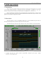
7.2 Description.
The logic analyzer viewer is an MSDOS application. It can be handled using the mouse or
the keyboard, though some operations require the use of the mouse.
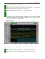
The following figure shows the logic analyzer screen, whose elements are described below.
•
A header with the text “UVI51 LOGIC ANALYZER” followed by the name –without
extension- of the displayed file.
18
UVI-51 User’s Manual (v5.0)
•
A bar of buttons placed in the upper left corner.
This button is used to exit the analyzer. It is equivalent to the Esc key.
This button is used to create a file in HPGL format corresponding to the chronograms
window (see below). It is equivalent to the 'p' (lowercase) key.
This button is used to show a help window. It is equivalent to '?' key.
This button is used to zoom in time scale. It is equivalent to '+' key.
This button is used to zoom out time scale. It is equivalent to '-' key.
This button is used to find a pattern from the current cursor position to the end of the
displayed block. When clicked while keeping the shift key pressed, the search is extended
outside the displayed block. These actions are equivalent to press the 'f' and 'F' keys
respectively. See section 7.3 for more details.
•
Chronograms window:
This window shows node chronograms. It includes 2 shift bars. The horizontal bar is used
to scroll through the time axis. The vertical bar is used to select the group of nodes currently
displayed. Bars are shifted using the following buttons:
This button is used to step time forward. It is equivalent to the right arrow key.
This button is used to step time backward. It is equivalent to the left arrow key.
19
UVI-51 User’s Manual (v5.0)
This button is used to go forward to the end of chronogram. It is equivalent to the ‘End’
key.
This button is used to go back to the beginning of chronogram. It is equivalent to the
‘Home’ key.
This button is used to scroll nodes up. It is equivalent to the ‘PgUp’ key.
This button is used to scroll nodes down. It is equivalent to the ‘PgDn’ key.
The bars can also be shifted by dragging with the mouse, or by clicking on the target
position.
Node labels and numbers are shown in the left side, followed by their respective search
patterns: X= don’t care, 0= low level, 1= high level. In the case of buses, the pattern is shown as
an hex number: X= don’t care, ?= undefined, other = hex value. Section 7.3 indicates how to
define and use search patterns.
The bottom part of this window shows two time scales, one absolute indicating simulation
time and the other relative to the logged data –zero for the first logged sample-.
A time cursor is also included. This cursor is shown as a vertical dashed line and has an
associated time value shown on its upper side. The cursor can be moved using the following keys
and/or
buttons combinations:
Shift
+
or Shift + right arrow key to move cursor to the right.
Shift
+
or Shift + left arrow key to move cursor to the left.
Shift
+
or Shift + ‘End’ key to move the cursor to the end of window.
Shift
+
or Shift + ‘Home’ key to move cursor to the beginning of window.
The cursor can also be dragged using the mouse or moved directly clicking on the target
position.
The time associated to cursor position is shown, by default, as absolute time. Clicking on
the cursor while keeping the shift key pressed will reset the cursor time to zero. This is useful for
time measurements. If the same operation is performed but the shift key is replaced by the control
key, the cursor recovers its absolute value.
Some operations, for example the display of very large and very active chronograms, can
take a lot of time. The operation can be canceled using the ‘Del’ key.
The bottom part of the analyzer display shows a help on buttons. Simply place the mouse
pointer over a button –without clicking- to view the related help.
7.3 Finding patterns in the chronograms.
The task of locating a specific portion of chronograms can be hard, specially if a long
simulation has been run. The Find utility can help to locate any portion defined by a characteristic
pattern. A pattern is a set of states (vector) related to a set of nodes. Before a search process is
initiated, a search pattern has to be defined.
20
UVI-51 User’s Manual (v5.0)
A pattern is defined assigning some node states to ‘0’ or ‘1’. The nodes whose state is
don’t care, must be assigned an ‘X’ value. Node patterns change cyclically every time the user
clicks them, according to the sequence ‘X, 0, 1’. The initial pattern is all don’t cares. If a bus has
been defined, its search pattern changes automatically every time the user changes the pattern of
the belonging nodes.
The user can also modify a bus pattern directly, by clicking on one of its hex digits. The
clicked digit is replaced by a red square. Then, the user can enter a new value (0,...F) using the
keyboard. If the user press the ‘X’ key, the four nodes that form that hex digit are marked as don’t
care. Any change in a bus pattern is updated automatically in the corresponding node patterns.
The question mark ‘?’ placed in a bus pattern digit indicates that at least one of its nodes
has been assigned as don’t care and at least another one has been assigned as ‘0’ or ‘1’.
Once
a
search pattern is defined, the search process is initiated by clicking the
or by pressing the ‘f’ (lowercase) key. The search begins at the current
magnifier button
cursor
position
and extends to the end of the window. The cursor is placed on the first
match found. For a search not limited to the current window keep the shift key pressed while
clicking the button, or press the ‘F’ (uppercase)- key.
If the cursor is already on a match, the next search will discard this match. This behavior
makes successive searches easier.
21
UVI-51 User’s Manual (v5.0)
APPENDIX A1: CNX Files Syntax
CNX files are ASCII files with two main blocks. The first block defines micro(s) while the
second one defines external peripherals.
The expression node number is used throughout this section in a Spice-like way, though with
some differences that must be considered:
•
Node numbers must be numbers between 0 and 201. The use of correlative numbers starting
with 2 is encouraged since this speeds up simulation.
•
Numbers 0 and 1 have special meanings:
•
Node 0 → Connection to ground, equivalent to a permanent logic level 0.
•
Node 1 → Connection to +Vdd through a pull-up resistor. Its logic level is 1, unless
connected to a 0 level (Wired-AND concept).
A1.1. Defining microcontrollers
Every micro in the system must be defined using a line with the following syntax:
Uprogram clockfreq xramsize romsize
where the initial U must be the first character in the line and has to be followed without blank
spaces by a source file name. This is the program to be run by the micro. Three parameters follow
indicating the clock frequency –in MHz- and the size of external data and program memories –in
bytes- respectively. The following ranges must be regarded:
1 <= clockfreq <= 100
8 <= xramsize <= 32768
32 <= romsize <= 8192
Once a micro has been defined, the user can add a set of lines in order to assign node
numbers to micro ports. The syntax must be:
Pxy=N
with the meaning ‘bit y of port x connected to node number N’. When the simulator finds this kind
of line, it assumes a reference to the last defined micro.
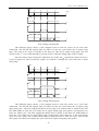
A1.2. Defining external peripherals
External peripherals are shown in the simulator system window (see section 6.1). The
definition of a peripheral in the CNX file must include the position where the user want the
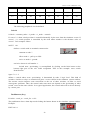
peripheral to be shown. This position is specified by a cell number between 1 and 32. The
following figure depicts the way cells are numbered.
22
UVI-51 User’s Manual (v5.0)
1
2
3
4
5
6
7
8
9
10
11
12
13
14
15
16
17
18
19
20
21
22
23
24
25
26
27
28
29
30
31
32
The following peripherals can be defined:
Switch
S<label> <common_node> <0_node> <1_node> <control>
If control > 0 then switch position is controlled manually by the user from the simulator screen. If
control < 0, switch position is controlled by the node whose number is the absolute value of
control. Two examples follow:
SOFF 7 1 0 1
defines a switch with its terminals connected to:
common to node 7
idle to node 1 –pull up to Vddactive to node 0 –groundand to be shown in cell number 1.
Switch state –positioning- is accomplished by clicking on the little button at the
bottom right part of the cell. Label assignment –OFF in this example- eases switch
identification.
Sgate 7 1 0 –5
defines a switch whose state –positioning- is determined by node 5 logic level. This kind of
switches -similar to relays or transmission gates- are not shown in the simulator system window.
The current version imposes some restrictions to the use of these switches, in order to avoid
convergence problems. Thus, the control node state must not depend on the positioning of other
switch –not even the same switch-. In a typical application, the control node will be driven directly
by a micro port.
Pushbutton (key)
K<label> <node_A> <node_B> <cell>
The pushbutton closes when depressed clicking the button shown in the simulator system window.
Example:
KINT 20 0 1
23
UVI-51 User’s Manual (v5.0)
defines a pushbutton connected between node 20 and ground. The simulator shows the pushbutton
in the cell number 1, where the user can depress it using the mouse.
Binary display (LED)
L<label> <anode_node> <cathode_node> <cell> [<color>]
The LED lights if anode_node is at logic level ‘1’ and cathode_node at ‘0’. A lighten LED
is shown painted with the indicated color. The default color is red. The following colors are
available:
red
yellow
green
blue
R
Y
G
B
For example:
LRxD 1 6 8 Y
defines a LED whose anode is pulled up to Vdd through a resistor and whose cathode is connected
to node number 6. The simulator will show it in the cell number 8. The figure depicts the LED
lightened using yellow color.
Hex display
H <0_node(LSB)> ... <3_node(MSB)> <-enable_node> <cell>
This display is equivalent to a common cathode 7 segment display preceded by a BIN to
HEX decoder. If the value applied to 0_node through 3_node inputs is restricted to the range 0 to
9, it can be used as a BCD to 7 segments decoder plus a common cathode display. If -enable_node
is at 1 level, the display is blank. Thus, a multiplexed display can be simulated.
For example:
H 10 11 12 13 0 5
defines a display with its data inputs connected to nodes 10, ... , 13 and its -enable input
permanently connected to ground. The display will be shown in cell number 5 as depicted.
The -enable terminal is placed under de display. The 4 data inputs are placed on left and
right sides beginning with the LSB in the left up corner, and following in counter-clock-wise.
LCD screen (serial)
D <CLK_node> <DAT_node> <LOAD_node> <cell>
The LCD screen displays 2 lines of 16 characters. It is controlled via a 3-wire synchronous
serial link. Commands are sent via the DAT terminal. The LCD screen has an internal shift
register that grabs the data present at DAT with the falling edge of CLK. When a falling edge is
present in LOAD, the LCD screen executes the command stored in the shift register.
24
UVI-51 User’s Manual (v5.0)
The LCD screen supports the following commands (bits are shown in the order they are
stored in the shift register and therefore the LSB must be sent first):
0 d7 d6 d5 d4 d3 d2 d1 d0
Writes the extended ASCII char given by d7...d0 in the current cursor position, either in overwrite
or insert modes (see commands 1100 and 1101).
1 0 0 a4 a3 a2 a1 a0
Moves cursor to the position a4...a0. (0= home, 31= end).
1010
Hides cursor.
1011
Shows cursor.
1100
Set mode to INSERT.
1101
Set mode to OVERWRITE.
1110
Deletes the character in the current cursor position and shifts all the characters placed at its right
to the left (like a common delete).
1111
Clears the whole screen and moves the cursor to position 0 (home).
Example: If the following bits are sent beginning with the right '0', the cursor hides.
1010
The following chronogram shows the suitable timing for the serial link. The falling edges of CLK
and LOAD are actives. The number of clock pulses (low level) equals the number of bits in the
command to be sent.
DAT
CLK
LOAD
Standard LCD Screen (parallel).
X <RS_node> <RW_node> <E_node> <D0_node> ... <D7_node> <cell>
25
UVI-51 User’s Manual (v5.0)
This screen is functionally equivalent to the de facto standard LCD screen of 2 lines by 16
characters (for example Trident MDLS 16265). However, some limitations exist which are
described below.
A node number must be indicated for every pin. In the case of a 4-bit data bus connection,
not connected pins must be assigned to node 1 (+VDD through a pull-up resistor). For example:
X 2 3 4 1 1 1 1 10 11 12 13 6
The simulator shows the LCD screen as follows:
The left-side column indicates the nodes where pins RS, RW, and E are connected. The
bottom row indicates the nodes where data lines are connected to (MSB first).
All the instructions (commands) in the standard set are available. However, the single-line
format (N= 0) is not supported.
The simulated LCD screen accepts instructions at any time. Therefore, reading the busy
flag returns always '1'.
UVI51 is an 'instruction level' simulator, that is, the minimum operation that can be
simulated is the execution of an instruction (cycle). The simulation of peripherals is also
performed cycle by cycle. Therefore, the chronograms required to control the screen are slightly
different from the real ones. Though this is not usually a problem, typical chronograms are
indicated as a reference.
The following figure shows a time diagram used to write the screen via an 8-bit data
connection. The RS and RW signals must be stable at least one cycle before the E signal rising
edge. The value to be written must be stable in the data bus at least one cycle before the E signal
falling edge, and remain stable at least one more cycle. The E signal must be at least one cycle at
high level. The RS and RW signals are permitted to change one cycle after the E signal rising edge.
26
UVI-51 User’s Manual (v5.0)
RS
cycles
t
RW
t
E
t
DBUS (DB0 - DB7)
value to be written
must be stable
t
8-bit writing time diagram
The following figure shows a time diagram used to read the screen via an 8-bit data
connection. The RS and RW signals must be stable at least one cycle before the E signal rising
edge. The value to be read is available in the data bus after the E signal rising edge. The bus
returns to the 3 rd state (VDD through a pull-up resistor) after the falling edge of the E signal.
Since the micro must read the bus while data are stable, the E signal must remain at least 2
cycles at high level. The RS and RW signals are allowed to change one cycle after the E signal
rising edge.
RS
cycles
t
RW
t
E
t
DBUS (DB0-DB7)
value to be read
is valid
t
8-bit reading time diagram
The following figure shows a time diagram used to write the screen via a 4-bit data
connection. The RS and RW signals must be stable at least one cycle before the E signal rising
edge (first pulse). The most significant nibble of the value to be written must be stable in the data
bus (DB7-DB4) at least one cycle before the E signal falling edge (first pulse), and remain for at
least one whole cycle. The least significant nibble must be stable in the data bus (DB7-DB4) at
least one cycle before the E signal falling edge (second pulse) and remain for at least one whole
cycle. For every pulse, the E signal must remain at high level for at least one cycle. The RS and
RW signals are allowed to change one cycle after the E signal rising edge (first pulse).
27
UVI-51 User’s Manual (v5.0)
RS
cycles
t
RW
t
E
t
DBUS (DB4-DB7)
value to be written
value to be written
must be stable
must be stable
(most significant nibble) (least significant nibble)
t
4-bit writing time diagram
The following figure shows a time diagram used to read the screen via a 4-bit data
connection. The RS y RW signals must be stable in the bus at least one cycle before the E signal
rising edge (first pulse). The most significant nibble of the value to be read is available in the bus
(DB7-DB4) after the E signal rising edge (first pulse). The bus returns to the 3 rd state (VDD
through a pull-up resistor) after the falling edge in the E signal (first pulse). The least significant
nibble of the value to be read is available in the bus (DB7-DB4) after the E signal rising edge
(second pulse). The bus returns to the 3 rd state (VDD through a pull-up resistor) after the falling
edge of the E signal (second pulse). For every pulse, the E signal must remain at least 2 cycles at
high level, so that the microcontroller can read the bus. The RS and RW signals are allowed to
change one cycle after the E signal rising edge (first pulse).
RS
cycles
t
RW
t
E
t
DBUS (DB4-DB7)
value to be read
is valid
(most significant nibble)
value to be read
is valid
(least significant nibble)
t
4-bit reading time diagram
Listings for writing and reading operations are included below, using pseudo-code (4-bits
mode only).
WRITING:
1) RS= {0,1} // 0 for instruction, 1 for memory (DDRAM or CGRAM).
28
UVI-51 User’s Manual (v5.0)
2) RW= 0.
3) E= 1.
4) Place in the bus the most significant nibble of the value to be written.
5) E= 0.
6) E= 1.
7) Place in the bus the least significant nibble of the value to be written.
8) E= 0.
9) Set the bus to 3 rd state (free for an eventual later read).
10) RS and RW can be modified if required.
READING:
1) RS= {0,1} // 0 for flag+address, 1 for memory (DDRAM or CGRAM).
2) RW= 1.
3) Be sure that the port lines used to read data are configured as inputs (1s).
4) E= 1.
5) Read the most significant nibble from the bus.
6) E= 0.
7) E= 1.
8) Read the least significant nibble from the bus.
9) E= 0.
10) RS and RW can be modified if required.
Logic Analyzer
Only one analyzer can be defined in a CNX file. The syntax is:
Afilename <tinitial> <tfinal>
where filename is the name of the file where the user wants the logged data to be stored. The
parameters tinitial and tfinal indicate the simulator times when the data logging will begin and end
respectively. The initial time is 0 by default. The final time is, by default, the end of simulation.
The user can not indicate a final time if the initial time is omitted.
Data logging is carried out by writing to a binary file. Data are registered using stamps.
When any node state changes, a stamp is registered. Each stamp includes a time indication and the
29
UVI-51 User’s Manual (v5.0)
state of all the nodes defined in the system. In order to avoid unlimited log file growth, the number
of stamps is restricted to 100,000. The equivalent file size depends on the number of nodes in the
system and is about 3 Mbytes. Would this limit be reached, the logging process is ended and the
log file closed.
The analyzer definition can be followed by a set of lines assigning labels to nodes and
defining buses.
Node labels
The user can assign labels to node numbers using the following syntax.
Nn label
where n is the node number and label the name given to the node. For example:
N5 CLK
assigns the name CLK to node number 5. This label will be displayed by both the simulator and
the analyzer replacing node number 5. Node labels defined prior to an analyzer definition are used
by the simulator but not by the logic analyzer.
Buses
The user can define a bus as a sorted set of nodes using the syntax:
Blabel nn n0 n1 n2 ...
where label is the bus identifier. The parameter nn indicates the bus depth –how many nodes it
consists of - and n0 n1 ... is a sorted list of nn node numbers beginning with the least significant
one. For example:
DATA 8 2 3 4 5 6 7 8 9
defines an 8-bit BUS named DATA whose LSB is node 2 and so on.
The relative position of the lines defining node labels and buses within the CNX file is important
because it determines their placements in the analyzer chronograms window.
APPENDIX A2: Customizing UVI-51
This appendix is not intended for novice users. The experienced users will find here an
explanation on how to customize the batch files used to call the editor and the assembler.
The editor is called by the batch file _EDIT.BAT, the full path and name of the file to be
edited being passed as a parameter. A typical BAT file for this purpose is:
@echo off
30
UVI-51 User’s Manual (v5.0)
edit %1
that calls the MSDOS edit program. In this case, both edit.com and qbasic.exe must be accessible
– their location directory must be included in MSDOS PATH-.
When the user requests UVI51 to assemble a source file, the batch file ASSEMBLE.BAT is
called. The source file name without an extension is passed as a parameter. The standard
ASSEMBLE.BAT file is
@echo off
uviens51 %1.src
whose second line call the UVI51 assembler.
In order to use Intel’s ASM51 assembler, the ASSEMBLE.BAT file could be:
@echo off
copy %1.src/A %1.srb/B
asm51 %1.srb object(%1.obj) print(%1.lst)
hayerror %1
if errorlevel 1 goto goout
oh %1.obj to %1.hex
pause
:goout
del %1.srb
Note: hayerror.exe is the name of an executable file that looks for errors in the LST file.
This file is customized for ASM51. For other assemblers, the user is encouraged to consult
the corresponding manuals.
In any case, only the assemblers that generate LST and HEX files compatible with those
generated by Intel’s assembler can be used.
APPENDIX A3: Technical support
The author does not guarantee the correctness of this software, nor accept any
responsibility for any loss derived of its use.
Furthermore, the author is not obligated to give present or future maintenance nor develop
new software versions.
Nevertheless, the author will try to answer short and well defined questions about UVI51
usage, at the following mail address.
31
UVI-51 User’s Manual (v5.0)
Alfredo del Río (UVI-51)
Dpto. Tecnología Electrónica
ETSII-Universidad de Vigo
36200 VIGO
SPAIN
and at the e-mail address:
[email protected]
indicating as subject UVI51.
The author encourage users to enclose the following information:
1) Requester’s name and occupation (University or College student, teacher, etc.).
2) E-mail address where the answer must be delivered (if different from sender).
3) Application where UVI51 is being or going to be used (teaching/learning at a specific level,
R&D, etc.).
4) Requester’s opinion about UVI51: Assessment, errors found, suggestions.
Thank you for using UVI51.
Vigo (Spain), December, 1999
Alfredo del Río.
32