1
PICDEM CAN-LIN 2
Development Kit
User’s Guide
© 2003 Microchip Technology Inc.
DS51334B
Note the following details of the code protection feature on Microchip devices:
•
Microchip products meet the specification contained in their particular Microchip Data Sheet.
•
Microchip believes that its family of products is one of the most secure families of its kind on the market today, when used in the
intended manner and under normal conditions.
•
There are dishonest and possibly illegal methods used to breach the code protection feature. All of these methods, to our
knowledge, require using the Microchip products in a manner outside the operating specifications contained in Microchip’s Data
Sheets. Most likely, the person doing so is engaged in theft of intellectual property.
•
Microchip is willing to work with the customer who is concerned about the integrity of their code.
•
Neither Microchip nor any other semiconductor manufacturer can guarantee the security of their code. Code protection does not
mean that we are guaranteeing the product as “unbreakable.”
Code protection is constantly evolving. We at Microchip are committed to continuously improving the code protection features of our
products. Attempts to break Microchip’s code protection feature may be a violation of the Digital Millennium Copyright Act. If such acts
allow unauthorized access to your software or other copyrighted work, you may have a right to sue for relief under that Act.
Information contained in this publication regarding device
applications and the like is provided only for your convenience
and may be superseded by updates. It is your responsibility to
ensure that your application meets with your specifications.
MICROCHIP MAKES NO REPRESENTATIONS OR
WARRANTIES OF ANY KIND WHETHER EXPRESS OR
IMPLIED, WRITTEN OR ORAL, STATUTORY OR
OTHERWISE, RELATED TO THE INFORMATION,
INCLUDING BUT NOT LIMITED TO ITS CONDITION,
QUALITY, PERFORMANCE, MERCHANTABILITY OR
FITNESS FOR PURPOSE. Microchip disclaims all liability
arising from this information and its use. Use of Microchip
devices in life support and/or safety applications is entirely at
the buyer’s risk, and the buyer agrees to defend, indemnify and
hold harmless Microchip from any and all damages, claims,
suits, or expenses resulting from such use. No licenses are
conveyed, implicitly or otherwise, under any Microchip
intellectual property rights.
Trademarks
The Microchip name and logo, the Microchip logo, Accuron,
dsPIC, KEELOQ, KEELOQ logo, microID, MPLAB, PIC,
PICmicro, PICSTART, PRO MATE, rfPIC and SmartShunt are
registered trademarks of Microchip Technology Incorporated
in the U.S.A. and other countries.
AmpLab, FilterLab, Linear Active Thermistor, Migratable
Memory, MXDEV, MXLAB, SEEVAL, SmartSensor and The
Embedded Control Solutions Company are registered
trademarks of Microchip Technology Incorporated in the
U.S.A.
Analog-for-the-Digital Age, Application Maestro, CodeGuard,
dsPICDEM, dsPICDEM.net, dsPICworks, ECAN,
ECONOMONITOR, FanSense, FlexROM, fuzzyLAB,
In-Circuit Serial Programming, ICSP, ICEPIC, Mindi, MiWi,
MPASM, MPLAB Certified logo, MPLIB, MPLINK, PICkit,
PICDEM, PICDEM.net, PICLAB, PICtail, PowerCal,
PowerInfo, PowerMate, PowerTool, REAL ICE, rfLAB, Select
Mode, Smart Serial, SmartTel, Total Endurance, UNI/O,
WiperLock and ZENA are trademarks of Microchip
Technology Incorporated in the U.S.A. and other countries.
SQTP is a service mark of Microchip Technology Incorporated
in the U.S.A.
All other trademarks mentioned herein are property of their
respective companies.
© 2003, Microchip Technology Incorporated, Printed in the
U.S.A., All Rights Reserved.
Printed on recycled paper.
Microchip received ISO/TS-16949:2002 certification for its worldwide
headquarters, design and wafer fabrication facilities in Chandler and
Tempe, Arizona; Gresham, Oregon and design centers in California
and India. The Company’s quality system processes and procedures
are for its PIC® MCUs and dsPIC® DSCs, KEELOQ® code hopping
devices, Serial EEPROMs, microperipherals, nonvolatile memory and
analog products. In addition, Microchip’s quality system for the design
and manufacture of development systems is ISO 9001:2000 certified.
DS51334B-page ii
© 2003 Microchip Technology Inc.
PICDEM™ CAN-LIN 2
DEVELOPMENT KIT
USER’S GUIDE
Table of Contents
Preface ........................................................................................................................... 1
Chapter 1. Introduction to the PICDEM CAN-LIN 2 Board
1.1 Introduction ..................................................................................................... 7
1.2 Highlights ........................................................................................................ 7
1.3 PICDEM CAN-LIN 2 Development Kit Contents ............................................ 7
1.4 Overview of the PICDEM CAN-LIN 2 Board .................................................. 8
1.5 PICDEM CAN-LIN 2 Board Features ............................................................. 9
1.1 CANKing Host Software ............................................................................... 12
Chapter 2. Getting Started with the PICDEM CAN-LIN 2 Board
2.1 Highlights ...................................................................................................... 13
2.2 Host Computer Requirements ...................................................................... 13
2.3 Using the PICDEM CAN-LIN 2 Board for the First Time .............................. 13
2.4 Checking the Board in Evaluation Mode ...................................................... 19
Chapter 3. Getting Started with the CANKing Software
3.1 Highlights ...................................................................................................... 21
3.2 Software Overview ....................................................................................... 21
3.3 Starting the Program .................................................................................... 21
3.4 Introduction to the Templates ....................................................................... 22
3.5 The Main Menu ............................................................................................ 22
3.6 The Output Window ...................................................................................... 23
3.7 Customizing Projects .................................................................................... 24
Chapter 4. Using the CANKing Templates
4.1 Highlights ...................................................................................................... 25
4.2 PIC® MCU Register View Template ............................................................. 25
4.3 The Basic Template ..................................................................................... 30
4.4 PIC18+CAN Evaluation Board Template ..................................................... 35
4.5 Template-Specific Variations in the Main Menu ........................................... 40
Chapter 5. Reconfiguring the PICDEM CAN-LIN 2 Hardware
5.1 Highlights ...................................................................................................... 41
5.2 Node Configurations ..................................................................................... 41
5.3 Oscillator Configurations .............................................................................. 42
5.4 Jumper Settings ........................................................................................... 42
5.5 Restoring the PICDEM CAN-LIN 2 Firmware ............................................... 43
© 2007 Microchip Technology Inc.
DS51334B-page iii
PICDEM™ CAN-LIN 2 Development Kit User’s Guide
Chapter 6. Troubleshooting
6.1 Highlights ...................................................................................................... 45
6.2 Common Problems ....................................................................................... 45
Appendix A. PICDEM CAN-LIN 2 Board Technical Information
A.1 Highlights ..................................................................................................... 47
A.2 PICDEM CAN-LIN 2 Block Diagram ............................................................ 47
A.3 PICDEM CAN-LIN 2 Board Schematics ...................................................... 48
Appendix B. FAQs on Configuring the PIC18FXX8X
B.1 Highlights ..................................................................................................... 55
B.2 FAQs ............................................................................................................ 55
Appendix C. PICDEM CAN-LIN 2 Software CD
C.1 Highlights ..................................................................................................... 57
C.2 What’s on the CD ......................................................................................... 57
Index .............................................................................................................................59
Worldwide Sales and Service .....................................................................................62
DS51334B-page iv
© 2007 Microchip Technology Inc.
PICDEM™ CAN-LIN 2
DEVELOPMENT KIT
USER’S GUIDE
Preface
NOTICE TO CUSTOMERS
All documentation becomes dated, and this manual is no exception. Microchip tools and
documentation are constantly evolving to meet customer needs, so some actual dialogs
and/or tool descriptions may differ from those in this document. Please refer to our web site
(www.microchip.com) to obtain the latest documentation available.
Documents are identified with a “DS” number. This number is located on the bottom of each
page, in front of the page number. The numbering convention for the DS number is
“DSXXXXXA”, where “XXXXX” is the document number and “A” is the revision level of the
document.
For the most up-to-date information on development tools, see the MPLAB® IDE on-line help.
Select the Help menu, and then Topics to open a list of available on-line help files.
INTRODUCTION
This chapter contains general information about this manual and contacting customer
support.
HIGHLIGHTS
Items discussed in this chapter are:
•
•
•
•
•
•
•
About This Guide
Warranty Registration
Recommended Reading
The Microchip Web Site
The Microchip Web Site
Development Systems Customer Change Notification Service
Customer Support
© 2007 Microchip Technology Inc.
DS51334B-page 1
PICDEM™ CAN-LIN 2 Development Kit User’s Guide
ABOUT THIS GUIDE
Document Layout
This document describes how to use the PICDEM™ CAN-LIN 2 Development Board
as a development system for the PIC18FXX8X family of microcontrollers. The manual
layout is as follows:
• Chapter 1. “Introduction to the PICDEM CAN-LIN 2 Board” – What the
PICDEM CAN-LIN 2 Board is, what makes it a desirable development tool and
what features are available.
• Chapter 2. “Getting Started with the PICDEM CAN-LIN 2 Board” – Describes
how to connect and begin to use the PICDEM CAN-LIN 2 board.
• Chapter 3. “Getting Started with the CANKing Software” – Gives a brief
overview of the CANKing host software and the concept of the predefined
templates.
• Chapter 4. “Using the CANKing Templates” – Provides a more detailed
description of the individual templates and how to use them.
• Chapter 5. “Reconfiguring the PICDEM CAN-LIN 2 Hardware” – Describes
various multi-node configurations of the board, and how to customize certain
features.
• Chapter 6. “Troubleshooting” – Provides information on solving common
problems.
• Appendix A. “PICDEM CAN-LIN 2 Board Technical Information” – Provides
the block diagram and detailed schematics of the PICDEM CAN-LIN 2 board.
• Appendix B. “FAQs on Configuring the PIC18FXX8X” – Provides a list of the
most commonly encountered issues when programming PIC18FXX8X
microcontrollers, as well as some solutions.
• Appendix C. “PICDEM CAN-LIN 2 Software CD” – Provides a summary of the
software on the accompanying CD-ROM.
• Index – Cross-reference listing of terms, features and sections of this document.
• Worldwide Sales and Service – gives the address, telephone and fax number
for Microchip Technology Inc. sales and service locations throughout the world.
DS51334B-page 2
© 2007 Microchip Technology Inc.
Preface
Conventions Used in This Guide
This manual uses the following documentation conventions:
DOCUMENTATION CONVENTIONS
Description
Arial font:
Italic characters
Initial caps
Quotes
Underlined, italic text with
right angle bracket
Bold characters
N‘Rnnnn
Text in angle brackets < >
Courier New font:
Plain Courier New
Represents
Examples
Referenced books
Emphasized text
A window
A dialog
A menu selection
A field name in a window or
dialog
A menu path
MPLAB® IDE User’s Guide
...is the only compiler...
the Output window
the Settings dialog
select Enable Programmer
“Save project before build”
A dialog button
A tab
A number in verilog format,
where N is the total number of
digits, R is the radix and n is a
digit.
A key on the keyboard
Click OK
Click the Power tab
4‘b0010, 2‘hF1
Italic Courier New
Sample source code
Filenames
File paths
Keywords
Command-line options
Bit values
Constants
A variable argument
Square brackets [ ]
Optional arguments
Curly brackets and pipe
character: { | }
Ellipses...
Choice of mutually exclusive
arguments; an OR selection
Replaces repeated text
Represents code supplied by
user
File>Save
Press <Enter>, <F1>
#define START
autoexec.bat
c:\mcc18\h
_asm, _endasm, static
-Opa+, -Opa0, 1
0xFF, ‘A’
file.o, where file can be
any valid filename
mcc18 [options] file
[options]
errorlevel {0|1}
var_name [,
var_name...]
void main (void)
{ ...
}
Documentation Updates
All documentation becomes dated, and this user’s guide is no exception. Since
MPLAB® IDE, MPLAB C1X and other Microchip tools are constantly evolving to meet
customer needs, some actual dialogs and/or tool descriptions may differ from those in
this document. Please refer to our web site to obtain the latest documentation available.
© 2007 Microchip Technology Inc.
DS51334B-page 3
PICDEM™ CAN-LIN 2 Development Kit User’s Guide
Documentation Numbering Conventions
Documents are numbered with a “DS” number. The number is located on the bottom of
each page, in front of the page number. The numbering convention for the DS Number
is: DSXXXXXA,
where:
XXXXX
=
The document number.
A
=
The revision level of the document.
WARRANTY REGISTRATION
Please complete the enclosed Warranty Registration Card and mail it promptly.
Sending in your Warranty Registration Card entitles you to receive new product
updates. Interim software releases are available at the Microchip web site.
RECOMMENDED READING
This user’s guide describes how to use the PICDEM CAN-LIN 2 Development Kit. The
data sheets contain current information on programming the specific microcontroller
devices.
MPLAB® IDE User’s Guide (DS51025)
Comprehensive guide that describes installation and features of Microchip’s MPLAB
Integrated Development Environment (IDE), as well as the editor and simulator functions in the MPLAB IDE environment.
MPASM™ User’s Guide with MPLINK™ and MPLIB™ (DS33014)
This user’s guide describes how to use the Microchip PIC® MCU MPASM assembler,
the MPLINK object linker and the MPLIB object librarian.
PIC® Mid-Range MCU Family Reference Manual (DS33023) and
PIC® 18C MCU Family Reference Manual (DS39500)
These manuals explain the general details and operation of the mid-range and
advanced MCU family architecture and peripheral modules. They are designed to
complement the device data sheets.
Microsoft® Windows® Manuals
This manual assumes that users are familiar with the Microsoft Windows operating
system. Many excellent references exist for this software program, and should be
consulted for general operation of Windows.
THE MICROCHIP WEB SITE
Microchip provides online support via our web site at www.microchip.com. This web
site is used as a means to make files and information easily available to customers.
Accessible by using your favorite Internet browser, the web site contains the following
information:
• Product Support – Data sheets and errata, application notes and sample
programs, design resources, user’s guides and hardware support documents,
latest software releases and archived software
• General Technical Support – Frequently Asked Questions (FAQs), technical
support requests, online discussion groups, Microchip consultant program
member listing
• Business of Microchip – Product selector and ordering guides, latest Microchip
press releases, listing of seminars and events, listings of Microchip sales offices,
distributors and factory representatives
DS51334B-page 4
© 2007 Microchip Technology Inc.
Preface
DEVELOPMENT SYSTEMS CUSTOMER CHANGE NOTIFICATION SERVICE
Microchip’s customer notification service helps keep customers current on Microchip
products. Subscribers will receive e-mail notification whenever there are changes,
updates, revisions or errata related to a specified product family or development tool of
interest.
To register, access the Microchip web site at www.microchip.com, click on Customer
Change Notification and follow the registration instructions.
The Development Systems product group categories are:
• Compilers – The latest information on Microchip C compilers and other language
tools. These include the MPLAB C18 and MPLAB C30 C compilers; MPASM™
and MPLAB ASM30 assemblers; MPLINK™ and MPLAB LINK30 object linkers;
and MPLIB™ and MPLAB LIB30 object librarians.
• Emulators – The latest information on Microchip in-circuit emulators.This
includes the MPLAB ICE 2000 and MPLAB ICE 4000.
• In-Circuit Debuggers – The latest information on the Microchip in-circuit
debugger, MPLAB ICD 2.
• MPLAB® IDE – The latest information on Microchip MPLAB IDE, the Windows®
Integrated Development Environment for development systems tools. This list is
focused on the MPLAB IDE, MPLAB SIM simulator, MPLAB IDE Project Manager
and general editing and debugging features.
• Programmers – The latest information on Microchip programmers. These include
the MPLAB PM3 and PRO MATE® II device programmers and the PICSTART®
Plus and PICkit™ 1 development programmers.
CUSTOMER SUPPORT
Users of Microchip products can receive assistance through several channels:
•
•
•
•
Distributor or Representative
Local Sales Office
Field Application Engineer (FAE)
Technical Support
Customers should contact their distributor, representative or field application engineer
(FAE) for support. Local sales offices are also available to help customers. A listing of
sales offices and locations is included in the back of this document.
Technical support is available through the web site at: http://support.microchip.com
© 2007 Microchip Technology Inc.
DS51334B-page 5
PICDEM™ CAN-LIN 2 Development Kit User’s Guide
NOTES:
DS51334B-page 6
© 2007 Microchip Technology Inc.
PICDEM™ CAN-LIN 2
DEVELOPMENT KIT
USER’S GUIDE
Chapter 1. Introduction to the PICDEM CAN-LIN 2 Board
1.1
INTRODUCTION
The PICDEM™ CAN-LIN 2 Development Kit has been revised for the evaluation or
development of CAN network nodes utilizing Microchip’s PIC18FXX8X family of
28 and 40-pin microcontrollers. This tool is ideal for beginning CAN designers, as well
as those new to the PIC18FXX8X family.
The Demonstration Board provides three nodes (two CAN and one LIN bus) that can
be configured in numerous ways through jumpers and component selection. The CAN
nodes implement basic input and output functionality, and can send and receive CAN
bus messages. The host software included with the kit allows fine manipulation of the
PIC18F4680 devices down to the bit level, as well as high-level control of the microcontroller. It also provides predefined templates for demonstration, evaluation and
development uses.
1.2
HIGHLIGHTS
This chapter discusses:
•
•
•
•
1.3
PICDEM CAN-LIN 2 Development Kit Contents
Overview of the PICDEM CAN-LIN 2 Board
PICDEM CAN-LIN 2 Board Features
CANKing Host Software
PICDEM CAN-LIN 2 DEVELOPMENT KIT CONTENTS
Your PICDEM CAN-LIN 2 Development kit contains the following items:
1. PICDEM CAN-LIN 2 Development Board, complete with three Microchip microcontrollers (two PIC18F4680 controllers and one PIC16C432) preprogrammed
with demo firmware.
2. A universal power supply (110-230 VAC input, 12 VDC output) and power cable
for the Development Board.
3. A male-to-female DB9 serial cable for use in communicating with the board.
4. The PICDEM CAN-LIN 2 CD-ROM with CANKing host software, User’s Guide
and other supporting documents.
5. A warranty registration card.
© 2007 Microchip Technology Inc.
DS51334B-page 7
PICDEM™ CAN-LIN 2 Development Kit User’s Guide
1.4
OVERVIEW OF THE PICDEM CAN-LIN 2 BOARD
Most demonstration or evaluation systems use a single microcontroller, and are
designed to show off that controller’s features. While this makes sense in most situations, it also means that users must set up several boards to evaluate even a simple
network of a few nodes. The drawbacks to this arrangement should be obvious.
In contrast, PICDEM CAN-LIN 2 provides three network nodes on one circuit board. By
using a common power supply, and allowing the nodes to be configured in multiple
ways, the process of evaluating and developing network nodes can be significantly
streamlined.
The three nodes on the PICDEM CAN-LIN 2 board are:
• Node0, a CAN node implemented with either a 28-pin PIC18F2585/2680 or 40-pin
PIC18F4585/4680 microcontroller. This node interfaces to the external host
computer through a standard serial (RS-232) interface, and is directly controlled
by the host software. It monitors both the on-board and external CAN busses, and
can be used for basic PIC18FXX8X evaluation/development.
• Node1, a CAN node also implemented with either a PIC18F2585/2680 or
PIC18F4585/4680 device. This node communicates with Node0 over the
on-board CAN bus. It also implements the CAN-to-LIN bus gateway to Node2
(below), and acts as the LIN bus master node. Like Node0, Node1 can also be
used for basic PIC18FXX8X evaluation/development.
• Node2, a LIN bus slave node, is implemented with the 20-pin PIC16C432
microcontroller with integrated LIN bus transceiver. It communicates to Node1 via
the LIN bus.
Both the CAN and LIN busses are routed off-board through a connector, which allows
the board to be connected to an external bus.
1.4.1
Benefits of Using the PICDEM CAN-LIN 2 Board
Putting three nodes on one board gives the developer some definite benefits:
MULTIPLE HARDWARE CONFIGURATIONS WITH ONE BOARD: Of course, the
PICDEM CAN-LIN 2 board accommodates a large selection of CAN and LIN node
combinations. When all three nodes are used, sixteen different combinations of microcontrollers are possible, depending on which sockets are populated for the CAN nodes.
In addition, users can implement any one of three oscillator configurations for the CAN
nodes, or easily add other hardware to the board using the prototyping area and
headers.
Many of these configuration changes are performed with jumpers, while others require
component additions or removals. The board configurations and jumper locations are
discussed in detail in Chapter 5. “Reconfiguring the PICDEM CAN-LIN 2 Hardware”
and Chapter 6. “Troubleshooting”.
EASIER CAN NODE EVALUATION: The CANKing host software, included with the
PICDEM CAN-LIN 2 Development Kit, allows for fast evaluation of CAN node operation,
as well as the CAN protocol. Using one of the included template sets, users can evaluate
everything from bit level status of registers to node operation and bus status. The host
software and the templates are discussed in detail in Chapter 3. “Getting Started with
the CANKing Software” and Chapter 4. “Using the CANKing Templates”.
ENHANCED CAN NODE DEVELOPMENT: Including two CAN nodes on the PICDEM
CAN-LIN 2 board provides an additional tool for developing PIC18FXX8X-based CAN
nodes, either by themselves or together. For example, a user might use the controller
in Node1 to prototype a CAN node, while using Node0 as a simple bus monitor (using
the basic template). Node0 could also be used as a tool to set or verify bit timings,
masks or filters.
DS51334B-page 8
© 2007 Microchip Technology Inc.
Introduction to the PICDEM CAN-LIN 2 Board
The possibilities are not limited to what can be developed with just the nodes on the
board, either. For example, Node0 can be included as part of a more complex developmental network of many CAN nodes, and serve as the “tap point” for monitoring the
entire network.
1.5
PICDEM CAN-LIN 2 BOARD FEATURES
As mentioned, the PICDEM CAN-LIN 2 board consists of two CAN nodes and one LIN
node. Node0 acts as the main node. It interfaces with the host software through a serial
connection (RS-232), and either executes commands from the host system or passes
them to Node1. Node0 also interfaces with the on-board LCD header. If an LCD is
connected, Node0 can display text messages under host software control.
Node1 also acts as a CAN node, and demonstrates a CAN-to-LIN bridge. This node is
controlled via Node0, which relays commands for Node1 from the host system. Node1
receives these messages and performs the appropriate actions. This node also acts as
a LIN master mode and provides CAN-to-LIN bridge functionality to Node2. As a LIN
master, it receives messages from Node0 and relays them to the LIN slave node.
Node2 is a LIN slave node implemented by the PIC16C432. This node contains an
integrated LIN bus transceiver. It waits for commands from Node1and performs the
appropriate actions.
As configured from the box, the behavior of the CAN nodes is determined by its
hardware configuration. While Node0 and Node1 both execute the exact same code,
the function of the node is decided by its hardware configuration. When either node is
reset, its firmware attempts to communicate with the external EEPROM. If the
EEPROM is found, the code assumes the role of Node0 and uses the USART to communicate with the host system. If the EEPROM is not found, it assumes the role of
Node1 and uses the USART for LIN bus communication. Since the EEPROM is
hard-wired to the Node0 controller, this essentially ensures that this controller will
always be Node0.
Node0 and Node1 are connected via the on-board CAN bus, which is also available to
an external CAN bus through a D-shell connector. Node1 and Node2 are connected via
the on-board LIN bus. Node1 uses a separate LIN transceiver while Node2 uses an
integrated LIN transceiver. The board routes the on-board LIN bus to a 3-pin header for
connection to external LIN devices.
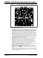
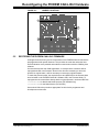
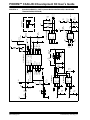
The overall layout of the board is shown in Figure 1-1.
© 2007 Microchip Technology Inc.
DS51334B-page 9
PICDEM™ CAN-LIN 2 Development Kit User’s Guide
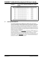
FIGURE 1-1:
THE PICDEM™ CAN-LIN 2 BOARD (TOP ASSEMBLY VIEW)
17
14
15
16
18
20
19
12
11
13
1a
5a
2a
5b
4a
4b
3
1b
2b
10
5c
6a
6b
7a
21
8
9b
9a
7b
21
21
22
The main features of the board include:
1. Node0 Microcontroller: The board is equipped with a pair of nested DIP sockets, designed to accommodate the 40-pin PIC18F4585/4680 (1a) or the 28-pin
PIC18F2585/2680 (1b); each includes an integrated CAN module. The Node0
microcontroller also handles the communications to the host computer (via
RS-232), as well as the external serial EEPROM and the optional LCD module.
2. Node1 Microcontroller: This is also a nested DIP socket pair that can accommodate either the PIC18F4585/4680 (2a) or PIC18F2585/2680 (2b). This node
communicates with Node0 and any external CAN nodes over the on-board CAN
bus. It also serves as the LIN master, and communicates to Node2 and other
external LIN nodes over the on-board LIN bus.
3. Node2 Microcontroller: This is a 20-pin DIP PIC16C432 with integrated LIN
bus transceiver. It acts as a LIN slave and transfers data to and from Node1.
4. Oscillators: Node0 and Node1 each support three different oscillator
configurations (crystal, RC and canned). The board is factory equipped with
25 MHz canned oscillators for both of the CAN nodes. If a different oscillator
type is required, the board hardware must be reconfigured (see
Section 5.3 “Oscillator Configurations” for more information). Node2 uses an
RC oscillator only (not shown); it cannot be reconfigured.
5. Reset Push Buttons: Each of the microcontrollers has its own Reset push
button switch, tied to the MCLR pin. Pressing the switch causes a hard controller
Reset.
6. CAN Node User-Defined Switches: Two push button switches are connected
to each the CAN nodes to simulate digital inputs. Their status can be monitored
through the host software.
DS51334B-page 10
© 2007 Microchip Technology Inc.
Introduction to the PICDEM CAN-LIN 2 Board
7. CAN Node Potentiometers: These analog potentiometers (7a and 7b) are
connected to Node0 and Node1, respectively. These potentiometers simulate
analog inputs for their controllers, and control the brightness of the
PWM-controlled LED on the other CAN node (i.e., the Node0 potentiometer
controls the brightness of Node1’s LED and vice versa). Their real-time status is
also displayed by the host software.
8. Node2 Potentiometer: This analog potentiometer is connected to Node2. When
Node2 is configured for “Poll Automatically” option, the real-time status of this
potentiometer is displayed by the host software.
9. CAN Node LED Banks: Both Node0 and Node1 are connected to their own
bank of nine LEDs: one 8-bit LED port and one PWM-controlled LED. The 8-bit
LED shows the (digital) status of PORTD of the controller, and can be modified
under software control. The output of the PWM-controlled LED is continuously
variable, and is determined by the value of the other CAN node’s potentiometer
(7a or 7b), as noted. For the LEDs to function, their associated LED enable
jumper (JP1 or JP2) must be installed.
10. Node2 LED Bank: An 8-bit LED port is connected to PORTB of the LIN slave
node and shows its (digital) status. The display can be modified under software
control. The LED enable jumper, JP4, must be installed for the bank to function.
11. CAN Transceivers: The MCP2551 transceivers (one for each CAN node)
convert the differential signal on the CAN bus to levels that are compatible with
the PIC18 microcontrollers.
12. LIN Transceiver: The MCP201 transceiver converts the high-voltage signals
from the LIN bus to levels compatible with the PIC16 microcontroller.
13. External EEPROM: A 24LC16 serial EEPROM is included for the use of
developers in creating a full range of prototype devices. This is a 16 Kbit device
which is programmable by a two-wire I2C™ interface. The EEPROM memory is
controlled by Node0. Its contents may be read or modified via the host software
interface.
14. RS-232 (DB9F) Port: A standard D-shell connector provides a serial connection
to control and monitor the Demonstration Board. Since it uses a standard 232
level shifter, this connector can also be used as a standard serial port for
prototype applications.
15. CAN Connector (DB9M): This connector allows the on-board CAN nodes to be
connected to an external CAN bus.
16. LIN Connector (3-pin) Pad: A space is provided to add a 3-pin connector,
allowing the on-board LIN node to connect with an external LIN bus.
17. ICD Connectors: These two 6-wire RJ-11 connectors allow the CAN Node
microcontrollers to be connected to an external programmer and programmed on
the board.
18. Power Connector: Power (12 VDC) is supplied to the board from the power
adapter through a 4-pin mini-DIN jack. Alternatively, external power can be
provided through the 2-pin terminal block. On-board regulators provide separate
+5 VDC sources for analog and digital circuits. Both inputs are protected from
accidental polarity reversal. Direct 12 VDC is also available to appropriate
circuits.
19. Power LED (Red): This is lit to show that power is being supplied to the
Demonstration Board.
20. LCD Connector: This 14-pin header allows the addition of a standard LCD
controller module (such as Hitachi HD4478 or equivalent) to the demonstration
board.
© 2007 Microchip Technology Inc.
DS51334B-page 11
PICDEM™ CAN-LIN 2 Development Kit User’s Guide
21. Prototype Headers: These connector pads are provided for users to directly
access the I/O port signals for all the microcontrollers. As an option, headers may
be installed in these locations.
22. MCU Prototype Area: This grid is provided for prototyping controllers that are
not supported by the existing sockets. The area is provided with connections for
analog and digital power (separate +5 VDC sources), VBAT for LIN (up to
+12 VDC) and ground connections.
1.1
CANKing HOST SOFTWARE
Included with the Development Kit is the CANKing host software. Developed by
Kvaser AB, the CANKing package allows users to examine and control the board’s
operation in detail, as well as monitor CAN node operations. Interfaces are
implemented through a series of three predesigned templates, which are grouped by
functionality (CAN node evaluation and control, board-level control, etc.). CAN-related
templates are designed around the CAN Kingdom upper-layer protocol primitives.
Previous experience with this CAN design system is helpful, but not strictly necessary.
Installation and overall operation of the host software is discussed in
Chapter 3. “Getting Started with the CANKing Software”. The CANKing templates
are detailed in Chapter 4. “Using the CANKing Templates”.
DS51334B-page 12
© 2007 Microchip Technology Inc.
PICDEM™ CAN-LIN 2
DEVELOPMENT KIT
USER’S GUIDE
Chapter 2. Getting Started with the PICDEM CAN-LIN 2 Board
2.1
HIGHLIGHTS
This chapter will cover the following topics:
• Host Computer Requirements
• Using the PICDEM CAN-LIN 2 Board for the First Time
• Checking the Board in Evaluation Mode
2.2
HOST COMPUTER REQUIREMENTS
To communicate with and program the PICDEM™ CAN-LIN 2 Development Board, you
must have a system that meets the following hardware and software requirements:
• PC-compatible system with an Intel® 80486 class or higher processor, or
equivalent
• A minimum of 16 MB RAM
• A minimum of 5 MB available hard drive space
• CD-ROM drive (for use with the accompanying CD)
• One available standard serial port, with a matching COM port available through
the operating system
• Microsoft® Windows® 95, or any 32-bit version of Microsoft Windows operating
system (Windows 98, Windows NT®, Windows 2000 or Windows XP)
2.3
USING THE PICDEM CAN-LIN 2 BOARD FOR THE FIRST TIME
For evaluating the PICDEM CAN-LIN 2 board, the simplest configuration uses a host
computer connected directly to the board using a crossover cable. Creating this setup
involves the following steps:
1. Installing the CANKing Host Software.
2. Connecting the PICDEM CAN-LIN 2 Development Board to the host system.
3. Starting the Host Software.
© 2007 Microchip Technology Inc.
DS51334B-page 13
PICDEM™ CAN-LIN 2 Development Kit User’s Guide
2.3.1
Installing the Host Software
The installation of the host software package is completely automated and does not
require any user intervention or configuration once the process is started. The process
is identical for all 32-bit Windows operating systems. Users with Windows NT-based
desktops (NT 4.0, 2000 and XP) should not need to have administrative rights to their
systems for this installation. Closing all background applications before proceeding is
helpful, but not required.
Note:
It is possible that some organizations may implement a desktop computer
policy sufficiently restrictive to prevent the user from loading any software
at all. In theory, this can be done with any 32-bit Windows operating
system on a network – including Windows 95. If this describes your
situation, contact your local Information Services provider for assistance
in installing this software.
To install the host software:
1. Insert the PICDEM CAN-LIN 2 Software CD into your system’s CD-ROM drive.
2. Double-click on My Computer, then on the icon for the CD-ROM.
3. Double-click on the wc32mchip_pic.exe icon. Installation will proceed
automatically and take 1-2 minutes.
Alternatively, run the installation by selecting Run from the Start menu. At the dialog
box, enter:
x:\wc32mchip_pic
where “x” is the drive letter of your CD-ROM.
The installation process will install the host software package, as well as the
templates and help files. By default, all files are installed by default in the directory
Program Files\Microchip under the root level of your hard drive. A shortcut for
the host software is also installed under Programs from the Start menu
(Programs > Microchip > CANKing).
Note:
2.3.2
Always use the suggested default path for installing the host software.
Because of certain software dependencies, it may not work correctly if
installed elsewhere.
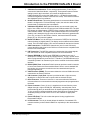
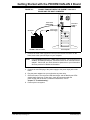
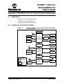
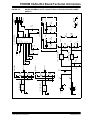
Connecting the PICDEM CAN-LIN 2 Board
The basic connections are shown in Figure 2-1.
1. Power-down the host system. (This isn’t strictly necessary, but it’s always a good
safety idea – particularly if you need to rearrange cables or move the system.)
2. Unbox and unwrap the board, and set it on a non-conductive surface near the
host system.
3. If they aren’t installed already, install the microcontrollers in their respective
sockets. Check that they are completely seated and that all pins are making
contact.
DS51334B-page 14
© 2007 Microchip Technology Inc.
Getting Started with the PICDEM CAN-LIN 2 Board
FIGURE 2-1:
CONNECTIONS BETWEEN THE PICDEM™ CAN-LIN 2
BOARD AND THE HOST COMPUTER
Serial Cable
(DB9 to DB9)
Serial Port
PICDEM™ CAN-LIN 2 Board
Serial Port
(COM1 or
COM2)
12 VDC from
Power Supply
Host Computer
4. Connect the serial cable (supplied in the kit) to the RS-232 connector on the
board, then to the open serial port on your computer.
Note:
If your available serial port is a DB25 male connector, you will need to use
a DB25F-to-DB9M port adapter, sometimes known as an “external modem
adapter”. Check with your local electronics parts store or your Information
Services provider for additional information.
5. Connect the mini-DIN plug of the power supply to the power input jack on the
board.
6. Plug the power adapter into your wall socket or power strip.
7. Check the board. The red power LED should light, and the Node0 port LEDs
should briefly flash once. If they don’t, check all connections with the
power supply and the board. For additional assistance, refer to
Chapter 6. “Troubleshooting”.
8. Power-up the host system.
© 2007 Microchip Technology Inc.
DS51334B-page 15
PICDEM™ CAN-LIN 2 Development Kit User’s Guide
2.3.3
Starting the Host Software for the First Time
With the software installed, and the PICDEM CAN-LIN 2 board connected, all you need
to do is to actually start the host software and confirm communications.
1. From the Start menu, select Programs > Microchip > CANKing;
OR
From a Command window (DOS® window on Windows 95/98), navigate to the
directory \program files\microchip, then enter:
wc32
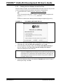
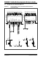
However it is started, the CANKing welcome dialog box appears (Figure 2-2).
FIGURE 2-2:
THE CANKing WELCOME DIALOG
2. Select the “Start using CANKing” option. Optionally, to remove the dialog from
future start-ups, check the Don’t ask me again box. Click on OK.
3. At the subsequent “Warning!” dialog, click on OK, I Know What I’m Doing to
proceed. Optionally, check Don’t show me this warning in the future to
remove this dialog from future start-ups.
Note:
The cautions against personal injuries in this dialog refer to those cases
where the PICDEM CAN-LIN 2 board is being used in the evaluation and
development of live automotive and industrial networks. Obviously, this
doesn’t apply to situations where the board is being used in isolation to
prototype network nodes.
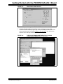
4. At the next dialog box (Figure 2-3), select the Template option under “Create a
New Project Using”. Click OK.
DS51334B-page 16
© 2007 Microchip Technology Inc.
Getting Started with the PICDEM CAN-LIN 2 Board
FIGURE 2-3:
CREATING A NEW PROJECT
5. At the “Templates” dialog, select PIC18+CAN Evaluation Board. Click on OK.
6. A series of smaller windows and dialog boxes is launched as part of the
Evaluation Board template (Figure 2-4). Go to the CANKing for Windows menu
at the top of the screen and select Options > PIC18+CAN... (you will need to
close the Tip of the Day window at center screen first).
FIGURE 2-4:
© 2007 Microchip Technology Inc.
THE EVALUATION BOARD TEMPLATE AT LAUNCH
(CANKing MAIN MENU BAR AT TOP LEFT)
DS51334B-page 17
PICDEM™ CAN-LIN 2 Development Kit User’s Guide
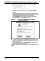
7. At the “Evaluation Board Options” dialog, select the following options from the
appropriate drop-down menus:
• Clock Frequency: 25000 kHz (25 MHz)
• COM Baud Rate: 38400 bps
• COM Port: (the port that the board is connected to)
Under Options for the Current Configuration, check Reset PIC18+CAN on
Open.
Click OK.
8. In the Evaluation Board window (which launched along with the other windows
of the Evaluation Board template), the “Connected” status indicator turns green,
and a message indicating a successful serial connection appears.
Click on Reset Board. The green light stays on, and the message below it
changes to “Eval Board is in Disable Mode” (Figure 2-5).
FIGURE 2-5:
THE EVALUATION BOARD WINDOW, SHOWING A
SUCCESSFUL CONNECTION
9. In the CAN Controller window, click on Go on Bus. The On Bus light turns green.
At the same time, the message in the Evaluation Board window changes to “Eval
Board is in Normal Mode”.
10. In the Evaluation Board window, click on Setup Modules. Output information
from the board appears in the Output window.
The PICDEM CAN-LIN 2 board is now ready to respond to control inputs from the host
software.
DS51334B-page 18
© 2007 Microchip Technology Inc.
Getting Started with the PICDEM CAN-LIN 2 Board
2.4
CHECKING THE BOARD IN EVALUATION MODE
While the board is connected to the host system and the host software is using the
Evaluation template, it may be useful to verify its operation. This is also a good way to
show off the board’s capabilities.
After following the instructions in Section 2.3 “Using the PICDEM CAN-LIN 2 Board
for the First Time”, do the following:
1. Slowly turn the Node0 potentiometer clockwise and counterclockwise. The right
most LED of Node1’s LED bank should brighten and dim. At the same time, the
Pot Value displayed in the Node0 Eval Board window should increase and
decrease, while the PWM Intensity indicator in the Node1 Eval Board window
should increase and decrease by the same amount.
2. Slowly turn the Node1 potentiometer clockwise and counterclockwise. The right
most LED of Node0’s LED bank should brighten and dim. At the same time, the
Pot Value displayed in the Node1 Eval Board window should increase and
decrease, while the PWM Intensity indicator in the Node0 Eval Board window
should increase and decrease by the same amount.
Note:
While this may seem anti-intuitive, using one node’s potentiometer to
affect the other’s LED does prove a point. For this demonstration, we
are showing that an analog input from one microcontroller can be
communicated across the CAN bus to control the PWM output of the
other microcontroller.
3. Click on any of the LED buttons in either of the CAN node’s windows. The
corresponding LED on the board should toggle on or off.
4. In the Node2 Eval Board window, select the Count LEDs check box. Both the
LED buttons in the window, as well as the Node2 LEDs on the board, should start
counting up in binary and in sync with each other.
If all of these tests worked, you are now ready to start working with the board.
© 2007 Microchip Technology Inc.
DS51334B-page 19
PICDEM™ CAN-LIN 2 Development Kit User’s Guide
NOTES:
DS51334B-page 20
© 2007 Microchip Technology Inc.
PICDEM™ CAN-LIN 2
DEVELOPMENT KIT
USER’S GUIDE
Chapter 3. Getting Started with the CANKing Software
3.1
HIGHLIGHTS
The items discussed in this chapter are:
•
•
•
•
•
•
3.2
Software Overview
Starting the Program
Introduction to the Templates
The Main Menu
The Output Window
Customizing Projects
SOFTWARE OVERVIEW
The CANKing host software provides a comprehensive interface to control the board’s
operation. To make things easier, the program uses three distinct, predefined templates
that perform specific functions.
Note:
3.3
Using the CANKing host software requires that the PICDEM™ CAN-LIN 2
board’s microcontrollers be programmed with the demo firmware. Since the
CAN firmware is designed to run on PIC18F4680 microcontrollers only,
using any configuration in Node0 and Node1 other than two PIC18F4680
microcontrollers precludes the use of CANKing host software. The board
can still be used in other configurations for prototype development.
STARTING THE PROGRAM
To run CANKing, select Programs > Microchip > CANKing. from the Start menu.
Alternatively, double-click on the CANKing icon or shortcut.
If you have not disabled them on the first use of the software, you will see the initial
CANKing Dialog and Warning window (see Section 2.3.3 “Starting the Host Software
for the First Time” for details). If they appear, click OK at these dialogs to continue.
At the Open a Project or Template dialog (simply titled “CANKing for Windows”), select
the Template option for creating a new project. (The other options listed are not
available in this version of CANKing and should be dimmed.) Click OK.
At the “Templates” dialog, select the appropriate template and click OK to launch it. You
can also directly launch the template by double-clicking on its icon.
If you have an alternate template or project you wish to use, select the Open an
Existing Project option at the “Open a Project” dialog. A standard Windows dialog
allows you to browse for the desired folder. Custom projects and templates are covered
in more detail in Section 3.7 “Customizing Projects”.
© 2007 Microchip Technology Inc.
DS51334B-page 21
PICDEM™ CAN-LIN 2 Development Kit User’s Guide
3.4
INTRODUCTION TO THE TEMPLATES
Much of the host software’s versatility comes from its use of predefined templates.
Because of the potential complexity of managing a microcontroller at the bit level – let
alone a network protocol such as CAN – the problem of organizing all the information
and controls that a user might need to evaluate and manage becomes a major
challenge. CANKing simplifies matters by grouping all the necessary controls for a
particular type of task into a template. Launching the template activates the necessary
individual control or monitor windows that are required for the task. Users have the
option to close or reopen particular windows as needed.
The individual templates and their controls are covered in detail in Chapter 4. “Using
the CANKing Templates”. A brief overview is given below.
3.4.1
PIC® MCU Register View Template
The PIC MCU Register template allows low-level control of Node0. It is typically used
to evaluate and test the PIC18FXX8X at the register and bit level. All of the registers
required for complete configuration of the CAN module are available in this template.
3.4.2
Basic Template
The Basic template is a high-level tool which focuses on CAN bus traffic. It is typically
used to observe the PIC18FXX8X while on the bus. The development of a CAN node
based on Node1 can be evaluated by using this template with Node0.
3.4.3
PIC18+CAN Evaluation Board Template
The Evaluation Board template provides real-time control of the entire board as a
demonstration tool. It allows users to control the LEDs for each of the nodes and
monitor in real time the status of the user push buttons and potentiometers.
3.5
THE MAIN MENU
Launching any of the templates, or opening any existing CANKing project, always
places a common toolbar at the top of the screen. The overall operation of CANKing is
controlled from here. The menu options available are, with a very few exceptions,
universal across all of the templates.
The File menu implements a standard set of Windows options. Users can create a new
project, save an existing project, open or reopen an existing saved project, close the
existing project without exiting CANKing and exit CANKing entirely.
The View menu allows the user to selectively open and close any of the windows and
dialogs available within the template. By default, each template opens only some of the
windows available to it. All of the windows available within a template are listed in the
View menu, allowing the user to select only those that are needed (or all windows, if
required).
The Messages menu is context-sensitive. Depending on the template, it either opens
(or shifts focus to) a specific configuration or message window, or selects the format
for the next CAN message to be sent. This is covered in more detail in
Section 4.5 “Template-Specific Variations in the Main Menu”.
The Options menu sets program wide operational options for CANKing. The
PIC18+CAN... selection configures hardware and communication options with the
board (see Figure 2-3). The Global... selection configures software options for
CANKing’s operation, such as the displayed numeric base of data and auto-save on
exit.
DS51334B-page 22
© 2007 Microchip Technology Inc.
Getting Started with the CANKing Software
The Window menu lists the open windows and dialogs, and lets the user bring any one
of the windows to the foreground. Unlike the View menu, this menu only shows those
windows which are active.
The Help menu provides access to indexed and interactive on-line product help, as well
as Internet links to Kvaser’s CANKing web site. Context-sensitive help is also available
by pressing F1.
The main menu toolbar (Figure 3-1) is the same for all templates. It provides standard
Windows toolbar buttons for creating a new project, and opening and saving an existing
project. Icons are also provided to go on and off the CAN bus; they are always present,
but functional only in the Basic and Evaluation templates.
FIGURE 3-1:
THE CANKing MAIN MENU
Go On Bus
Save Project
Open Existing Project
Create New Project
3.6
Go Off Bus
THE OUTPUT WINDOW
Common to both Basic and PIC18+CAN Evaluation templates is an Output window,
which displays the messages that are received and transmitted by Node0. This window
can be reconfigured to display messages in different formats. The formats are changed
using a combination of the Message Formatter dialog box and the right mouse button.
The Message Formatter window (titled “Select Formatter”) selects one or more of several
predefined formats for the window. The format type may be specific to a particular usage
(e.g., a CANKing’s page interpreter or a LIN bus message interpreter) or a generic text
format. More than one formatter may be selected, and their order of display may be
arranged at will. Many of the formats can be fine-tuned with their own configuration
options. For additional information, see Section 4.3.3 “Select Formatters Window”.
Using the right mouse button in this window brings up a menu with several options:
• Options allows the user to set the font used in the window, as well as the
maximum number of lines available in the window’s buffer.
• Fixed Positions effectively assigns a slot for each message identifier. As
messages with the same ID are received or transmitted, they overwrite the contents of the previous message with the same ID. Used in conjunction with the
delta time feature, the frequency of each message type can be observed.
• Copy to Clipboard copies the contents of the window’s buffer to the Windows
clipboard.
• Clear empties the window and its buffer.
© 2007 Microchip Technology Inc.
DS51334B-page 23
PICDEM™ CAN-LIN 2 Development Kit User’s Guide
FIGURE 3-2:
3.7
TYPICAL OUTPUT WINDOW (STANDARD TEXT FORMAT
SHOWN)
CUSTOMIZING PROJECTS
The templates furnished with the CANKing host software provide a quick way to
connect to the PICDEM™ CAN-LIN 2 board and examine its operation. As you gain
experience with the board and the software, however, you may want to customize your
environment. For example, you may want to launch a different set of controls than
those that a particular template uses as its default. Alternatively, you may want to use
different communications settings. The host software accommodates these needs by
allowing users to save CANKing projects with their particular settings, preserving both
hardware and window configurations.
To save a configuration, use the File > Save As menu option. CANKing allows you to
save either as a project (.wcc file extension), or a new template (.wct extension). A
standard Windows dialog permits you to browse folders for the desired location.
To open a previously saved project, either choose the “Open an Existing Project” from
the dialog box, or use the File > Open menu option. A standard Windows dialog box
permits you to browse folders for the desired file.
DS51334B-page 24
© 2007 Microchip Technology Inc.
PICDEM™ CAN-LIN 2
DEVELOPMENT KIT
USER’S GUIDE
Chapter 4. Using the CANKing Templates
4.1
HIGHLIGHTS
The items discussed in this chapter are:
•
•
•
•
4.2
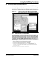
PIC® MCU Register View Template
The Basic Template
PIC18+CAN Evaluation Board Template
Template-Specific Variations in the Main Menu
PIC® MCU REGISTER VIEW TEMPLATE
This template allows low-level control of Node0. It is typically used to evaluate and test
the PIC18FXX8X microcontroller at the bit level. All of the registers required for
complete configuration are available in this template.
Values for buffer and control registers can be changed on both the byte and bit levels.
To modify the register on a byte level, enter the value in the boxes next to the register
names. Notice that the bit values will reflect the entered byte values.
To modify the registers at the bit level, double-click the desired bit. The bit will toggle
for each double-click and the byte representation will be reflected next to the register
name. The bit boxes are only modifiable when unshaded. Shaded bit boxes are
read-only bits.
FIGURE 4-1:
© 2007 Microchip Technology Inc.
PIC® MCU REGISTER VIEW TEMPLATE (WHOLE SCREEN
VIEW SHOWING THE AVAILABLE WINDOWS AT START-UP)
DS51334B-page 25
PICDEM™ CAN-LIN 2 Development Kit User’s Guide
4.2.1
PIC18+CAN Evaluation Board
This window is functionally available in all three templates, but is named and configured
in a slightly different manner for each. In each template, it displays the current communication status with the board. When a successful connection is detected, the “Eval
Board Status” LED turns green and displays a “connected” message. The window also
shows the current COM port setting and any log messages as the host software
communicates with the board.
In the PIC MCU Register template, the window provides three control buttons. Reset
Board causes a Reset of the board’s firmware, and erases all previous settings. Save
Reg saves the current register values as a HEX file; a standard Windows dialog allows
the user to browse for the file location. Load Reg restores previously saved register
values from a HEX file, and also uses a Windows dialog to search for the file’s location.
FIGURE 4-2:
4.2.2
PIC18+CAN EVALUATION BOARD WINDOW
(REGISTER TEMPLATE VERSION, BOARD NOT
CONNECTED)
PIC18+CAN Message Filters
This window is used to set up and test mask and filter combinations with different
message identifiers. Each mask and filter can be tested without actually writing the configuration to Node0. This is done to allow the user to test different configurations
against message identifiers that would appear on the bus. When the desired mask and
filter combinations are achieved, the values can be written to the Node0 by clicking the
Write button.
Note:
DS51334B-page 26
The masks and filters can be written only when the Node0 is in
Configuration mode.
© 2007 Microchip Technology Inc.
Using the CANKing Templates
FIGURE 4-3:
4.2.3
MESSAGE FILTER WINDOW
PIC18+CAN Physical Layer
The Physical Layer window is where the CAN bus rate is configured. The user has
bit-level control of the three BRGCON registers (BRGCON1, BRGCON2 and
BRGCON3), which sets up all items required for CAN bit timing including the time
quanta (TQ), bit segments, the Synchronization Jump Width (SJW) and the Baud Rate
Prescaler (BRP).
The calculated bit rate is shown at the bottom of the window. For this calculation to be
valid, the oscillator value must be correct. To change the oscillator value, select
Options->PIC18+CAN... from the main menu.
The BRGCON registers can be modified only when Node0 is in Configuration mode.
The bit will be shaded and cannot be modified in other modes of operation.
FIGURE 4-4:
© 2007 Microchip Technology Inc.
PHYSICAL LAYER WINDOW
DS51334B-page 27
PICDEM™ CAN-LIN 2 Development Kit User’s Guide
4.2.4
PIC18+CAN Receive Buffer
This window contains all of the buffer contents for the receive buffers including
RXBnCON, the identifier registers and the data registers.
RXB0CON and RXB1CON are the only registers in this window that are not read-only,
as indicated by the unshaded bit locations. These two registers set up the receive
modes and enables or disables the hardware double-buffer function.
The Receive Buffer windows allows users to select one buffer to view at a time. Multiple
Receive Buffer windows can be opened for simultaneous viewing by holding down the
Shift key while selecting the Receive Buffer option from the Windows menu
(Messages > PIC18+CAN Eval Board > Receive Buffer).
FIGURE 4-5:
4.2.5
RECEIVE BUFFER WINDOW
PIC18+CAN Status Window
The PIC18+SCAN Status window displays the contents of the CANSTAT register, the
COMSTAT register and the counts for the receive and transmit error counters. The condition of the registers are also shown (for example, a CANSTAT value of 80h displays
the condition as Configuration mode with no interrupts pending).
The window also contains controls to clear overrun conditions for each of the receive
buffers.
FIGURE 4-6:
DS51334B-page 28
PIC18+CAN STATUS WINDOW
© 2007 Microchip Technology Inc.
Using the CANKing Templates
4.2.6
PIC18+CAN Transmit Buffer
This window controls the buffer contents for the three transmit registers, including
TXBnCON, the identifier registers and the data registers.
Like the other register windows, the Transmit window maps the byte values to the bit
boxes. Entering data into the “CAN ID:” box maps to multiple registers (SIDH, SIDL,
EIDH and EIDL). For example, entering 1FFFFFFF in the “CAN ID:” box maps all ‘1’s
to SIDH, SIDL, EIDH and EIDL.
Like the Receive Buffer window, the Transmit Buffer window allows users to select one
buffer to view at a time. Multiple Transmit Buffer windows can be opened for
simultaneous viewing by holding down the Shift key while selecting the Transmit Buffer
option from the Windows menu (Messages > PIC18+CAN Eval Board > PIC18+CAN
Transmit Buffer).
FIGURE 4-7:
© 2007 Microchip Technology Inc.
TRANSMIT BUFFER WINDOW
DS51334B-page 29
PICDEM™ CAN-LIN 2 Development Kit User’s Guide
4.2.7
PIC18+CAN Configuration
This window displays and can directly control the contents of the CAN Control and
Peripheral Interrupt registers (CANCON, CIOCON, PIE3, PIR3 and IPR3). These are
the control and flag registers for the PIC18FXX8X microcontrollers.
A complete discussion of the function of these registers is beyond the scope of this
manual. Interested readers are referred to the “PIC18F2585/2680/4585/4680 Data
Sheet” (DS39625) for more information.
FIGURE 4-8:
4.3
PIC18+CAN CONFIGURATION WINDOW
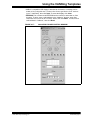
THE BASIC TEMPLATE
The Basic template is a high-level tool which focuses on CAN bus traffic. The user only
has high-level control of Node0 (i.e., no direct register control) which includes:
•
•
•
•
•
Configuring the bus rate
Changing modes of operation (Configuration and Normal)
Configuring a Transmit register (the register number is predefined)
Transmitting messages
Resetting Node0
Other functions of the Basic template are receiving messages, saving transmitted messages, starting timed transmissions and observing the bus loading. Details of these
functions can be found later in this section under the details of the individual windows.
This template would typically be used as a simple bus monitor that could be used to
evaluate the PIC18FXX8X on a CAN bus, or assist in development by monitoring how
Node1 is operating.
By default, the Basic template configures Node0 to receive ALL messages. The user
has the option to maintain Node0 configurations when switching templates by selecting
Options > PIC18+CAN... and deselecting the Reset PIC18+CAN on Opening check
box. Keep in mind that deselecting this box may create unforeseen problems if the
Node0 was not configured properly previously.
DS51334B-page 30
© 2007 Microchip Technology Inc.
Using the CANKing Templates
FIGURE 4-9:
4.3.1
THE BASIC TEMPLATE (WHOLE SCREEN VIEW SHOWING
THE AVAILABLE WINDOWS AT START-UP)
PIC18+CAN Evaluation Board
This window is similar in function to the Evaluation Board window in the PIC MCU
Register template (Section 4.2.1 “PIC18+CAN Evaluation Board”) in displaying the
current communication status of the board. For the Basic template, there is only one
control, the Reset Board button. It resets the firmware and writes power-on default
values to all of Node0’s CAN registers.
FIGURE 4-10:
© 2007 Microchip Technology Inc.
PIC18+CAN EVALUATION BOARD WINDOW
(BASIC TEMPLATE VERSION)
DS51334B-page 31
PICDEM™ CAN-LIN 2 Development Kit User’s Guide
4.3.2
PIC18+CAN Controller
This window provides information about the status of the bus, including nominal bus
loading, status of node (on or off the bus), and bus bit rate. The tabs at the top of the
window select between Bus Statistics and Bus Parameters pages.
On the Bus Statistics page, the bus loading, bus parameters and bus status can be
viewed. The bus loading shows the nominal load on the CAN bus as a percentage and
as a number as well as the total number of messages sent and received. The bus
parameters reflect the parameters set in the Bus Parameters view (i.e., bit rate, number of TQ, bit segment lengths and the location of the sample point). The Bus Statistics
shows the mode of operation and error states; this is also where the controls to put the
board On Bus (normal operation) or Off Bus (Configuration mode) are located.
Options on the Bus Parameters page allow the user to configure the bus rate, the sample point, the Synchronization Jump Width (SJW) and switching between Normal and
Listen Only modes of operation.
FIGURE 4-11:
DS51334B-page 32
PIC18+CAN CONTROLLER WINDOW
© 2007 Microchip Technology Inc.
Using the CANKing Templates
4.3.3
Select Formatters Window
This window determines the format of the displayed data in the Output window.
CANKing provides a number of predefined general and specialized format options for
data display. Many of these formats can, in turn, be fine-tuned with specific configuration options. The default is “Standard Text Format” which displays the message data as
normal data.
To add a formatter for the Output window, select an option from the “Available
Formatters” spin box, and click on the Use button. Alternatively, you can double-click
on the item. The formatter is successfully selected when it appears in the Active
Formatters window and its check box is selected.
To deactivate a formatter, select the item from the “Active Formatters” window and click
the Remove button. You can also temporarily deactivate an option by deselecting the
check box next to it.
To change the order that formatters are applied to the Output window, select a formatter
in the “Active Formatters” window and click on the Up or Down buttons.
The properties of the formatter can be changed by pressing the Properties button
while the selection is highlighted in the “Active Formatters” list. The properties of the
“Standard Text Format” are the numeric base of the display (octal, decimal or hexadecimal) and whether or not to display the message time-stamp as a running total or
as delta time. Many of the other formatters have their own unique configuration
properties (e.g., filter limits, message interpreters).
FIGURE 4-12:
4.3.4
MESSAGE FORMATTERS WINDOW
Output Window
The Output window is discussed in detail in Section 3.6 “The Output Window”.
© 2007 Microchip Technology Inc.
DS51334B-page 33
PICDEM™ CAN-LIN 2 Development Kit User’s Guide
4.3.5
History List
This window is used to collect transmitted messages for saving to a file. It is not opened
by default when opening a new template, but by selecting View > History List from the
main menu. Once opened, every transmitted message is captured in the History List
window for saving to a file, if desired. Each line consists of Identifier, Data Len and Data
Byte D0 through Data Byte D7. One or more messages can be selected for
retransmission. There is also a button for sending all the captured messages.
The History List window works in conjunction with the Timed Transmission window.
Messages can be retransmitted once, or continually at defined intervals. See the Timed
Transmission window (Section 4.3.6 “Timed Transmission”) for more details.
FIGURE 4-13:
4.3.6
HISTORY LIST WINDOW
Timed Transmission
The Timed Transmissions window is used to send the messages in the History List,
either once, or continually at timed intervals.
The One-Shot mode sends the selected (in the History List window) messages, one
time, each time the send buttons are pressed in the History List window.
The Cyclic selection sends the selected messages at regular intervals (from 1 ms to
10 s). The interval is set with the fixed-interval spin box.
The other Message Timing selections (Just-in-Time and Manual) are not available in
this version of the software.
FIGURE 4-14:
DS51334B-page 34
TIMED TRANSMISSION WINDOW
© 2007 Microchip Technology Inc.
Using the CANKing Templates
4.4
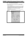
PIC18+CAN EVALUATION BOARD TEMPLATE
For most users, this is the very first template used when the PICDEM™ CAN-LIN 2
board is first set up and configured. It provides real-time control of the board’s
interactive features, and serves as the demo application for the on-board controls. The
individual Board Evaluation windows allow users to, among other things, toggle the
LEDs and monitor the real-time status of the push button switches and potentiometers.
FIGURE 4-15:
4.4.1
THE EVALUATION BOARD TEMPLATE (WHOLE SCREEN
VIEW SHOWING THE AVAILABLE WINDOWS AT START-UP)
Putting the Board in Evaluation Mode
Unlike the other templates, the PIC18+CAN Evaluation Board template requires
additional action by the user beyond a firmware Reset. This involves initializing that
section of the firmware which allows interactive control of the board’s features which
are not available when operating with the other templates. The initial setup described
in Section 2.3 “Using the PICDEM CAN-LIN 2 Board for the First Time” describes
the process in detail. If the board is already connected, however, it is only necessary to
do the following:
1. Open a new project using the Evaluation Board template.
2. In the PIC18+CAN Controller window, click Go on Bus.
3. In the PIC18+CAN Evaluation Board window, click Setup Modules. This
command causes multiple CAN messages to be transmitted and initializes all
nodes on the board.
The interactive features of the board are now available.
© 2007 Microchip Technology Inc.
DS51334B-page 35
PICDEM™ CAN-LIN 2 Development Kit User’s Guide
4.4.2
PIC18+CAN Evaluation Board Window
As with its counterparts in the other templates, this window displays the current communication status with the board. In this template, there are two control buttons. Reset
Board resets the firmware and writes power-on default values to all CAN registers.
Setup Modules initializes the firmware for the Interactive (Demonstration) mode.
FIGURE 4-16:
4.4.3
PIC18+CAN EVALUATION BOARD WINDOW
(EVALUATION BOARD TEMPLATE VERSION)
Node0 Eval Board (Control) Window
This window controls the interactive features on the Node0. Once initialized, this
window displays the correct status for the user-defined devices connected to Node0.
Node0 has the most interactive features, which means that this control window is the
largest of the three. From top to bottom, the controls are:
• Pot Value: This indicator is updated in real time to display the approximate position of the Node0 potentiometer. The value is also displayed in numerical format,
ranging from 0 to 1000 (approximately).
• PWM Intensity: This indicator shows the output of the PWM module in relative
terms, from minimum to maximum. It also shows the value numerically, ranging
from 0 to 1000 (approximately); this value is controlled by, and should match that
of, the Node1 potentiometer in the Node1 Eval Board window. The relative value
should also correspond to the brightness of the ninth LED, which is controlled by
the PWM module’s output.
• Push Button Status: The two indicators (btn0 and btn1) show the status of the
node’s user-defined push buttons. Pressing the buttons on the board will change
the indicators.
• LED Status: These eight buttons control and indicate the status of the first
8 LEDs of the LED bank (the ninth LED is controlled by Node1’s potentiometer).
Clicking on any of the buttons will toggle the corresponding LED on or off. The
LED enable jumper (JP3) must be installed for this feature to work.
DS51334B-page 36
© 2007 Microchip Technology Inc.
Using the CANKing Templates
• LCD: If a compatible LCD display is attached at the header, a message can be
written to it by using this area. To send a line of text, type into the “text:” text box
(up to 7 characters), then click Send. To erase the display, click Clear.
• EEPROM: The on-board serial EEPROM can be read from, and written to, from
this area. To write, enter a valid address in the “Address:” text box, enter data
values into one or more of the “Content:” boxes, then click Write. To read, enter a
valid address in “Address:”, then click Read.
FIGURE 4-17:
© 2007 Microchip Technology Inc.
Node0 EVAL BOARD CONTROL WINDOW
DS51334B-page 37
PICDEM™ CAN-LIN 2 Development Kit User’s Guide
4.4.4
Node1 Eval Board (Control) Window
This window controls Node1, the second CAN and LIN master node. When the board
is properly initialized, this window will also display the correct Module Status.
The interactive features are:
• Pot Value and PWM Intensity: These function identically to their counterparts for
the Node0 Eval Board Control window, except these refer to Node1. The PWM
intensity displayed and brightness of the ninth LED is controlled by the Node0
potentiometer, the value of which is displayed in the Node0 Eval Board window.
• Push Button Status: These are identical in function to Node0.
• LED Status: These are also identical to Node0.The LED enable jumper (JP4)
must be installed for this feature to work.
FIGURE 4-18:
DS51334B-page 38
NODE1 EVAL BOARD CONTROL WINDOW
© 2007 Microchip Technology Inc.
Using the CANKing Templates
4.4.5
Node2 Eval Board (Control) Window
This window shows real-time status of Node2, the LIN slave node.
Its features are:
• Poll automatically: When this check box is selected, the status of the Node2
potentiometer is monitored in real time and shown on the Pot Value display. Like
the other nodes, the value is also reported numerically.
• Count LEDs: Checking this box causes the Node2 LEDs to count up in binary
sequence (least significant digit on the left). The LEDs on the board and the Eval
window display count synchronously.
• LED Status: Like the other nodes, the LEDs for Node2 can also be individually
toggled on and off. For this feature (and the Count LEDs) to work, the LED
enable jumper (JP4) must be installed.
FIGURE 4-19:
4.4.6
NODE2 EVAL BOARD CONTROL WINDOW
PIC18+CAN Controller
This window is identical to the PIC18+CAN Controller window in the Basic template
(Section 4.3.2 “PIC18+CAN Controller”).
4.4.7
Select Formatters
This window is identical to the Message Formatters window in the Basic template
(Section 4.3.3 “Select Formatters Window”).
4.4.8
History List
This window is identical to the History List window in the Basic template
(Section 4.3.5 “History List”).
4.4.9
Timed Transmission
This is identical in form and function to the Timed Transmission window in the Basic
template (Section 4.3.6 “Timed Transmission”).
4.4.10
Output Window
The Output window is discussed in Section 3.6 “The Output Window”.
© 2007 Microchip Technology Inc.
DS51334B-page 39
PICDEM™ CAN-LIN 2 Development Kit User’s Guide
4.5
TEMPLATE-SPECIFIC VARIATIONS IN THE MAIN MENU
For the most part, the options available from the CANKing main menu are identical in
all three template views. The few exceptions are described below. Only two menu items
will be discussed in this section, as the others are self explanatory.
Messages Menu
In the Basic and PIC18+CAN Evaluation templates, the Messages menu selects the
CAN message type to be transmitted. Each option opens a dialog box for configuring
the message; the dialog is unique to the message type.
Two message options are available: Universal or CAN Kingdom. The Universal option
allows the user to send standard generic-format messages using a normal (up to eight
byte), integer, long integer, 32-bit floating point or string page format. The
CAN Kingdom option lets the user transmit a message that adheres to the
CAN Kingdom higher layer protocol in one of 20 pre-defined King’s page formats, or a
default letter format.
In the PIC Register template, the Messages menu provides alternate access to the
various buffer and register configuration windows; these are available as submenu
options from the single menu option (PIC18+CAN Eval Board).
Options Menu
All of the templates offer the Global and PIC18+CAN... options in the Options menu.
These are used to configure communications with the board and global features of
CANKing, and are discussed in Section 3.5 “The Main Menu”.
The Basic and P Evaluation templates also include the King’s Pages option. Selecting
this allows the user to set a default King’s envelope and city/group address.
Note:
The oscillator frequency must be set in software to match the hardware so
the software can configure the bit timing registers correctly. The formulas
for bit timing contain an oscillator frequency. Refer to the
“PIC18F2585/2680/4585/4680 Data Sheet” for further details.
The options menu contains the configurable properties of both the hardware and the
software.
The default numeric base is selected by Options > Global. Auto-save switches are also
contained here.
Options > PIC18+CAN... is where the COM port is selected, and where the oscillator
frequency is set in software. This menu also contains a switch that determines whether
or not the Node0 controller will be reset on file open. This feature is for those users who
want to switch between templates without changing the PIC18FXX8X configuration
(e.g., masks and filters are set to receive ALL messages in the Basic template unless
this box is deselected).
DS51334B-page 40
© 2007 Microchip Technology Inc.
PICDEM™ CAN-LIN 2
DEVELOPMENT KIT
USER’S GUIDE
Chapter 5. Reconfiguring the PICDEM CAN-LIN 2 Hardware
5.1
HIGHLIGHTS
This chapter covers the following:
•
•
•
•
5.2
Node Configurations
Oscillator Configurations
Jumper Settings
Restoring the PICDEM CAN-LIN 2 Firmware
NODE CONFIGURATIONS
The PICDEM CAN-LIN 2 board can be operated in many different configurations; only
a few of the possibilities are listed here. Most of these can be implemented without any
changes to the board; some may require the addition of some components or wiring.
Access to the external LIN bus will require the addition of a LIN bus connector at the
pads provided for J4 (item 16 in Figure 1-1).
5.2.1
Two CAN Nodes, One LIN Node, Embedded System
This is the default configuration. The two CAN nodes (Node0 and Node1) are
connected via the on-board CAN bus, while Node1 and Node2 are connected via the
on-board LIN bus. There are no external CAN or LIN bus connections.
This configuration can be used for evaluation or development. For design evaluation,
use one of the three templates to monitor or control the board. For development, use
Node1 for the development of applications; Node0 can then be used with the CANKing
software to monitor the development node. If required, Node1 may also communicate
with Node2.
5.2.2
Two CAN Nodes, One LIN Node, Distributed System
In this configuration, external CAN and LIN bus devices can be connected to the
on-board bus.
This configuration can be used for evaluation or development, using a similar approach
as an embedded system configuration (above).
5.2.3
Two CAN Nodes, Embedded System
In this configuration, Node2 is deactivated by removing the PIC16C432 controller from
its socket (with the power off, of course). If required, the circuit traces between the
Node1 USART pins and the stand-alone LIN bus transceiver may be cut, and an extra
RS-232 line driver may be added.
In Development mode, Node0 can be used to monitor Node1.
5.2.4
Two CAN Nodes, Distributed System
This configuration connects both on-board CAN nodes to an external CAN bus.
In Evaluation mode, Node0 can be used to monitor the external bus. In Development
mode, Node0 can be used to monitor both Node1 and the external bus.
© 2007 Microchip Technology Inc.
DS51334B-page 41
PICDEM™ CAN-LIN 2 Development Kit User’s Guide
5.3
OSCILLATOR CONFIGURATIONS
The PICDEM CAN-LIN 2 Board is designed to accommodate three different types of
oscillators for the PIC18FXX8X device-based nodes:
• Crystal-controlled oscillator
• RC oscillator
• Self-contained oscillator module (“canned” oscillator)
There are two oscillator sections on the board, one for each of the CAN controllers. As
shipped from the factory, the board is configured with two 25 MHz canned oscillators.
If a different clock frequency is desired, it is only necessary to remove the existing
oscillator modules and insert new ones.
To implement the other options, it will be necessary for users to make changes to the
board.
5.3.1
Crystal Oscillator
The on-board oscillator module(s) (Y2 and/or Y3) must be removed from their sockets.
Either one (or both) of the CAN controllers can be configured to use a crystal oscillator.
Pads, Y1 and Y4 (for Node0 and Node1, respectively), have been provided to add a
crystal. Depending on frequency and crystal used, capacitors may also need to be
added at pads, C24/C25 (Node0) and C30/C31 (Node 1). It is the user’s responsibility
to select values for these components to obtain a frequency compatible with the
controller. If the RC oscillator option has been previously used, it will be necessary to
remove the RC network components.
5.3.2
RC Oscillator
The on-board oscillator module(s) (Y2 and/or Y3) must be removed from their sockets.
The RC network for the oscillator is not provided and must be added by the user. Each
CAN controller has pads provided for an RC network. Pads, R21/C27 (for Node0) and
R22/C29 (for Node1), are provided for the addition of these components. It is the user’s
responsibility to select values for these components to obtain a frequency compatible
with the controller.
5.4
JUMPER SETTINGS
There are several jumpers provided for configuring the hardware operation of the
PICDEM CAN-LIN 2 board. Their functions are listed in Table 5-1 and locations are
shown in Figure 5-1.
TABLE 5-1:
DS51334B-page 42
JUMPER DESCRIPTION
Number
Board ID
Function
1
JP3
Connects 120 ohm terminating resistor to the CAN bus
2
JP1
LED enable for Node0
3
JP2
LED enable for Node1
4
JP4
LED enable for Node2
© 2007 Microchip Technology Inc.
Reconfiguring the PICDEM CAN-LIN 2 Hardware
FIGURE 5-1:
JUMPER LOCATIONS
1
4
2
5.5
3
RESTORING THE PICDEM CAN-LIN 2 FIRMWARE
As shipped from the factory, the microcontrollers on the PICDEM CAN-LIN 2 board are
preprogrammed with special firmware. This provides the code that makes the Interactive Evaluation mode possible and enables communication with the CANKing host
software.
As users develop their own CAN applications, it is likely that the controllers will be
reprogrammed with new firmware. Should it ever become necessary to return the
board to its original state, it will be necessary to restore the original firmware.
To make this process easier, the required source and HEX files for the firmware have
been included on the PICDEM CAN-LIN 2 Software CD in the Firmware folder. To
reprogram the microcontrollers directly with the original firmware, use these HEX files:
• cannode.hex: for Node0 and Node1 devices (PIC18F4680 only)
• linnode.hex: for the Node2 device (PIC16C432)
Users should follow the procedure appropriate for their device programmer and
development environment.
© 2007 Microchip Technology Inc.
DS51334B-page 43
PICDEM™ CAN-LIN 2 Development Kit User’s Guide
NOTES:
DS51334B-page 44
© 2007 Microchip Technology Inc.
PICDEM™ CAN-LIN 2
DEVELOPMENT KIT
USER’S GUIDE
Chapter 6. Troubleshooting
6.1
HIGHLIGHTS
This chapter discusses the following:
• Common Problems
6.2
COMMON PROBLEMS
1. The Power LED is not lit.
Check the PICDEM CAN-LIN 2 board for power:
• Verify that the power supply is plugged in and the wall outlet has power. If
battery connection is used, verify that the correct polarity is used.
• Check that voltage is available (12 VDC) at the plug. If the original power
supply is not being used, check for appropriate voltage (12 VDC).
• Check that the regulated voltage (5 VDC) is available at the connectors at the
prototype area of the board.
2. The host software cannot communicate with the board.
Check that the board is receiving power (see issue 1 above).
Check the serial cable for proper connections to the board and the computer.
Verify that the cable is connected to the correct serial port on the computer. If
necessary, verify the serial cable by swapping in another cable that is known to
be good.
Verify through Windows Device Manager (accessed through the System applet
in the Control Panel) that the selected COM port is recognized by the operating
system and is working.
Verify that you are using the correct serial port. Check that the COM port you
have selected in the terminal software is actually the physical port that the serial
cable is connected to.
Verify that the Node0 LEDs flash briefly on Reset or power-up of the board.
If you are using the optional LCD module, verify that the text “PIC CAN” is briefly
displayed on Reset or power-up, and an underscore cursor is displayed.
3. The board is operational, but neither of the CAN nodes are recognized on
an external network.
See Appendix B. “FAQs on Configuring the PIC18FXX8X” for the most
common CAN troubleshooting hints.
© 2007 Microchip Technology Inc.
DS51334B-page 45
PICDEM™ CAN-LIN 2 Development Kit User’s Guide
NOTES:
DS51334B-page 46
© 2007 Microchip Technology Inc.
PICDEM™ CAN-LIN 2
DEVELOPMENT KIT
USER’S GUIDE
Appendix A. PICDEM CAN-LIN 2 Board Technical Information
A.1
HIGHLIGHTS
This chapter will cover the following topics:
• PICDEM CAN-LIN 2 Block Diagram
• PICDEM CAN-LIN 2 Board Schematics
A.2
PICDEM CAN-LIN 2 BLOCK DIAGRAM
FIGURE A-1:
PICDEM™ CAN-LIN 2 DEVELOPMENT BOARD FUNCTIONAL
BLOCK DIAGRAM
Data EEPROM
Potentiometer
User
Push Buttons
LEDs
I/O Bus for
Prototype
Node0
PIC18F2585/2680
or
PIC18F4585/4680
RS-232
Interface
RS-232
Connector
ICD
Connector
LCD
CAN Transceiver
CAN bus
Connector
Potentiometer
User
Push Buttons
Node1
PIC18F2585/2680
or
PIC18F4585/4680
LEDs
LEGEND:
Single Line
Connections
© 2007 Microchip Technology Inc.
ICD
Connector
LIN Transceiver
LIN bus
Connector
Node2
PIC16C432
I/O Bus for
Prototype
Potentiometer
Multi-line
Connections
Optional
Peripherals
I/O Bus for
Prototype
LEDs
DS51334B-page 47
DS51334B-page 48
AGND
1
2
1
2
50k
R46
4
3
SWITCH
S9
4
3
SWITCH
S7
330
R45
R17
4.7k
+5V
R15
4.7k
+5V
RA5_1
C17
.1 μF
470
SW_1_2
SW_1_1
R44
SW_1_2
SW_1_1
C43
.1 μF
+5V
R42 470
R43 470
R2
22k
+5V
RA6_1
OSC1_1
RA5_1
RA4_1
RA3_1
RA2_1
RA1_1
RA0_1
ICSP_1_VPP
RB7_1
RB6_1
RB5_1
RB4_1
RB3_1
RB2_1
RB1_1
RB0_1
RA4_1
RA5_1
RA3_1
RA2_1
RA1_1
RA0_1
ICSP_1_VPP
C42
.1 μF
RD3/PSP3 22
RD2/PSP2 21
RD1/PSP1 20
RD0/PSP0 19
RC7/RX/DT 26
25
RC6/TX/CK
RC5/SD0 24
4 RA2/AN2/VREF5 RA3/AN3/VREF+
6 RA4/TOCKI
7 RA5/AN4/SS
33 RB0/INT0
34 RB1/INT1
U11
RC6 17
RC7 18
19 VSS
VSS
8
RC2 13
RC3 14
RC0 11
RC1 12
RB6/PGC 27
RB7/PGD 28
RB4 25
RB5/PGM 26
RB2/CANTX 23
RB3/CANRX 24
RC4 15
RC5 16
OSC1
RA5
RA4
RA3
RA2
RA1
RA0
MCLR
RB0/INT0 21
RB1/INT1 22
PIC18F2680
OSC1/CLKIN 13
RC7_1
RC6_1
RC5_1
RC4_1
RC3_1
RC2_1
RC1_1
RC0_1
RB7_1
RB6_1
RB5_1
RB4_1
RB3_1
RB2_1
RB1_1
RB0_1
OSC1_1
RA6_1
RC0_1
RA6/OSC2 14
RC1_1
RC0/T1OSO 15
RC2_1
RC3_1
RC4_1
RC5_1
RC6_1
RC7_1
RD0_1
RD1_1
RD2_1
RD3_1
RD4_1
RD5_1
RD6_1
RD7_1
RE0_1
RE1_1
RE2_1
RC2/CCP1 17
RC1/T1OSI 16
10 RA6/OSC2
9
7
6
5
4
3
2
1
20 VDD
31 VSS
40 RB7/PGD
12 VSS
38 RB5/PGM
39 RB6/PGC
37 RB4
RC4/SDI/SDA 23
RC3/SCK 18
RD5/PSP5 28
RD4/PSP4 27
2 RA0/AN0/CVREF
3 RA1/AN1
35 RB2/CANTX
36 RB3/CANRX
RD7/PSP7 30
RD6/PSP6 29
RE2/CS/AN7 10
RE1/WR/AN6 9
RE0/RD/AN5 8
PIC18F4680
1 MCLR/VPP
11 VDD
32 VDD
U10
FIGURE A-2:
R5
33k
AVDD
4
3
SWITCH
S12
R11
4.7k
+5V
A.3
1
2
+5V
D39
PICDEM™ CAN-LIN 2 Development Kit User’s Guide
PICDEM CAN-LIN 2 BOARD SCHEMATICS
BOARD SCHEMATIC, PART 1 (Node0 MICROCONTROLLERS AND
ASSOCIATED PARTS)
© 2007 Microchip Technology Inc.
© 2007 Microchip Technology Inc.
AGND
1
2
1
2
50k
R52
R6
33k
4
3
SWITCH
S8
4
3
SWITCH
S10
330
R51
4
3
SWITCH
S13
R16
4.7k
+5V
R15
4.7k
+5V
RA5_2
C44
.1 μF
470
SW_2_2
SW_2_1
R49
R50
4.7k
SW_2_2
SW_2_1
C46
.1 μF
+5V
R42 470
R43 470
R2
22k
+5V
RA6_2
OSC1_2
RA5_2
RA4_2
RA3_2
RA2_2
RA1_2
RA0_2
ICSP_2_VPP
RB7_2
RB6_2
RB5_2
RB4_2
RB3_2
RB2_2
RB1_2
RB0_2
RA4_2
RA5_2
RA3_2
RA2_2
RA1_2
RA0_2
ICSP_2_VPP
C45
.1 μF
+5V
RD3/PSP3 22
RD2/PSP2 21
RD1/PSP1 20
RD0/PSP0 19
RC7/RX/DT 26
25
RC6/TX/CK
RC5/SD0 24
4 RA2/AN2/VREF5 RA3/AN3/VREF+
6 RA4/TOCKI
7 RA5/AN4/SS
33 RB0/INT0
34 RB1/INT1
U13
RC6 17
RC7 18
19 VSS
VSS
8
RC2 13
RC3 14
RC0 11
RC1 12
RB7/PGD 28
RB5/PGM 26
RB6/PGC 27
RB3/CANRX 24
RB4 25
RC4 15
RC5 16
OSC1
RA5
RA4
RA3
RA2
RA1
RA0
MCLR
RB0/INT0 21
RB1/INT1 22
RB2/CANTX 23
PIC18F2680
OSC1/CLKIN 13
RC7_2
RC6_2
RC5_2
RC4_2
RC3_2
RC2_2
RC1_2
RC0_2
RB7_2
RB6_2
RB5_2
RB4_2
RB3_2
RB2_2
RB1_2
RB0_2
OSC1_2
RA6_2
RC0_2
RA6/OSC2 14
RC1_2
RC0/T1OSO 15
RC2_2
RC3_2
RC4_2
RC5_2
RC6_2
RC7_2
RD0_2
RD1_2
RD2_2
RD3_2
RD4_2
RD5_2
RD6_2
RD7_2
RE0_2
RE1_2
RE2_2
RC2/CCP1 17
RC1/T1OSI 16
10 RA6/OSC2
9
7
6
5
4
3
2
1
20 VDD
31 VSS
40 RB7/PGD
12 VSS
38 RB5/PGM
39 RB6/PGC
37 RB4
RC4/SDI/SDA 23
RC3/SCK 18
RD5/PSP5 28
RD4/PSP4 27
2 RA0/AN0/CVREF
3 RA1/AN1
35 RB2/CANTX
36 RB3/CANRX
RD7/PSP7 30
RD6/PSP6 29
RE2/CS/AN7 10
RE1/WR/AN6 9
RE0/RD/AN5 8
PIC18F4680
1 MCLR/VPP
11 VDD
32
VDD
U12
FIGURE A-3:
AVDD
1
2
+5V
D40
PICDEM CAN-LIN 2 Board Technical Information
BOARD SCHEMATIC, PART 2 (Node1 MICROCONTROLLERS AND
ASSOCIATED PARTS)
DS51334B-page 49
DS51334B-page 50
+5V
SWITCH
3
2
C21
.1 μF
RB3_2
RB2_2
C14
.1 μF
RB3_1
RB2_1
+5V
RS
RXD
VCC
VREF
CANL
GND CANH
TXD
5
6
7
8
4
3
2
1
RS
RXD
VCC
VREF
CANL
GND CANH
TXD
5
6
7
8
U5 MCP2551
4
3
2
1
U3 MCP2551
C40
0.1 μF
R39
4.7k
4.7k
R14
CAN_L
CAN_H
MCLR_3
RB3_3
RB2_3
RB1_3
RB0_3
IN4750 27V RA4_3
10 nF
RA3_3
RA2_3
D30
C39
4
S11
20k
R26
1
D36
TP2
LIN bus
VBAT
RB3
RB2
RB1
RB0/INT
VSS
1
MCLR/VPP
RA0/AN0
J3
5
4
3
2
1
DE9P318
9
8
7
6
2
20
11
12
13
14
15
16
17
18
19
R12 120
RB4
RB5
RB6
RB7
VDD
OSC2/CLKO
OSC1/CLKI
JP3
RA4/TOCKI
RA3/AN3
RA2/AN2/VREF RA1/BACT
LIN bus
R13
4.7k
10
9
8
7
6
5
4
3
2
1
U7 PIC16C432
R25
330
RC6_2
RC7_2
RC5_2
RB4_3
RB5_3
RB6_3
RB7_3
TP6
RA0_3
RA1_3
R24
50k
C34
33 pF
R23
4.7k
+5V
TP5
TP4
4
3
2
1
1
2
3
4
SDA
SCL
WP
Vcc
5
6
7
8
RX
WAKE
VDD
TX
INH
VSUP
LIN
GND
8
7
6
5
U8 MCP201
GND
A2
A1
A0
U6 24LC64_DIP
C32
.1 μF
+5V
TP3
C33
.1 μF
VBAT
VBAT
R53
100k
+5V
LIN bus
VBAT
J4
LIN bus
RC4_1
RC3_1
C23
.1 μF
C41
10 nF
R27
1k
D35
VBAT
R38
4.7k
D31
IN4750
27V
R37
4.7k
+5V
3
2
1
OPTIONAL
FIGURE A-4:
+5V
VBAT
R9
33k
+5V
PICDEM™ CAN-LIN 2 Development Kit User’s Guide
BOARD SCHEMATIC, PART 3 (Node2 MICROCONTROLLER, LIN AND CAN
TRANSCEIVERS, EEPROM)
© 2007 Microchip Technology Inc.
GND
NC/OE
OUT
VCC
© 2007 Microchip Technology Inc.
4
2
OUT
VCC
MDC-034
3
1
1
2
J5
J9
GND
NC/OE
+12 VDC
GND
7
1
8
14
8
D37
D34
+5V
C26
.1 μF
C28
.1 μF
14
P1
VBAT
C13
22 μF
+
OSC1_2
OPTIONAL
OSC1_1
OPTIONAL
VBAT
C29
33 pF
R22
4.7k
+5V
C27
33 pF
R21
4.7k
+5V
1 μF
C38
+5V
C36
1 μF
IN
COM
2
OUT
1
C16
.1 μF
1
IN
2
COM
OUT
3
VR1 TO-220POS
3
VR2 LM78L05ACZ
1 μF
C37
RC7_1
RC6_1
+
C15
10 μF
C19
10 μF
+
C18
.1 μF
P10
C20
.1 μF
P11
C24
22 pF
P9
+5V
15
16
8
13
7
D27
RED
R7
470
+5V
C25
22 pF
RA6_1
OSC1_1
+5V
C22
Y4
C31
22 pF
P7
9
8
7
6
RA6_2
OSC1_2
DE9S318
J14
GND
R3 0 ohm
C30
22 pF
5
4
3
AGND
.1 μF
20 MHz
OPTIONAL
GND
VCC
R2IN
R1IN
T2OUT
AVDD
V-
V+
C2-
C2+
C1-
C1+
R2OUT
R1OUT
T2IN
20 MHz
Y1
1 μF
C35
6
2
5
4
3
1
9
12
10
T1OUT
2
T1IN
14
11
1
U1 MAX232CPE
FIGURE A-5:
Y3 XTAL-OSC
7
1
Y2 XTAL-OSC
+5V
PICDEM CAN-LIN 2 Board Technical Information
BOARD SCHEMATIC, PART 4 (USART, OSCILLATOR OPTIONS AND POWER
SUPPLY)
DS51334B-page 51
DS51334B-page 52
RC2_1
RD7_1
RD6_1
RD5_1
RD4_1
D17
D16
D15
D14
D13
D12
D11
D10
D9
9
8
7
6
5
4
3
2
1
2
1
JP1
R41
820
R40
10k
+5V
470 ohm
10
R19
+5V
RC5_1
RC1_1
RC0_1
RC2_2
RD7_2
RD6_2
RD5_2
RD4_2
RD3_2
RD2_2
RD1_2
RD0_2
1 VSS
2 VCC
3 VEE
4 RS
6 E
5 R/W
7 DB0
D26
D25
D24
D23
D22
D21
D20
D19
D18
LCD_2X7
LCD1
9
8
7
6
5
4
3
2
1
2
DB7 14
DB5 12
DB6 13
DB3 10
DB4 11
DB1 8
DB2 9
1
JP2
470 ohm
10
R20
RA3_1
RA2_1
RA1_1
RA0_1
OPTIONAL
RB7_1
RB6_1
RB5_1
RB4_1
RB3_1
RB2_1
RB1_1
RB0_1
D8
D7
D6
D5
D4
D3
D2
D1
9
8
7
6
5
4
3
2
1
2
1
JP4
470 ohm
10
R32
FIGURE A-6:
RD3_1
RD2_1
RD1_1
RD0_1
PICDEM™ CAN-LIN 2 Development Kit User’s Guide
BOARD SCHEMATIC, PART 5 (LEDS AND LCD DISPLAY OPTION)
© 2007 Microchip Technology Inc.
© 2007 Microchip Technology Inc.
Node1
RB6_2
RB7_2
+5V
ICSP_2_VPP
6
5
4
3
2
1
6
5
4
3
2
1
J2
J1
RE1_2
RD7_2
RD5_2
RD3_2
RD1_2
RC7_2
RC5_2
RC3_2
RC1_2
RB7_2
RB5_2
RB3_2
RB1_2
RA6_2
RA4_2
RA2_2
RA0_2
RE1_1
RD7_1
RD5_1
RD3_1
RD1_1
RC7_1
RC5_1
RC3_1
RC1_1
RB7_1
RB5_1
RB3_1
RB1_1
RA6_1
RA4_1
RA2_1
RA0_1
20
22
24
26
28
30
19
21
23
25
27
29
35
36
34
18
17
33
16
15
32
14
13
31
12
36
35
11
34
33
10
32
31
9
30
29
8
28
27
7
26
25
6
24
23
5
22
21
4
20
19
2
18
17
3
16
15
1
14
13
10
8
6
4
2
12
J7
J6
11
9
7
5
3
1
RE2_2
RE0_2
RD6_2
RD4_2
RD2_2
RD0_2
RC6_2
RC4_2
RC2_2
RC0_2
RB6_2
RB4_2
RB2_2
RB0_2
RA5_2
RA3_2
RA1_2
RE2_1
RE0_1
RD6_1
RD4_1
RD2_1
RD0_1
RC6_1
RC4_1
RC2_1
RC0_1
RB6_1
RB4_1
RB2_1
RB0_1
RA5_1
RA3_1
RA1_1
Node2
RB7_3
RB5_3
RB3_3
RB1_3
RA4_3
RA2_3
RA0_3
13
14
12
10
9
11
8
7
4
2
6
J13
5
3
1
MCLR_3
RB6_3
RB4_3
RB2_3
RB0_3
RA3_3
RA1_3
FIGURE A-7:
Node0
RB6_1
RB7_1
+5V
ICSP_1_VPP
PICDEM CAN-LIN 2 Board Technical Information
BOARD SCHEMATIC, PART 6 (PROTOTYPE HEADERS AND CONNECTORS)
DS51334B-page 53
PICDEM™ CAN-LIN 2 Development Kit User’s Guide
TABLE A-1:
SIGNALS USED IN THE PICDEM™ CAN LIN 1 SCHEMATIC
Signal Name
CAN_H, CAN_L
Differential high and low CAN bus signals
ICSP_1_VPP or
ICSP_2_VPP
ICSP™ programming voltage and Reset for the designated
controller:
1 – CAN Node0
2 – CAN Node1
LIN bus
Differential LIN bus signal
MCLR_3
Reset signal for LIN node (PIC16C432)
SW_1_n or SW_2_n
Push button input from switch n for the designated controller:
1 – CAN Node0
2 – CAN Node1
RXn_1, RXn_2 or RXn_3
Bit n of PORTx for the designated controller:
1 – CAN Node0
2 – CAN Node1
3 – LIN Node (PIC16C432)
VBAT
LIN bus battery voltage (+9 to +12 VDC)
TABLE A-2:
DS51334B-page 54
Function
LCD CONTROLLER HEADER
Pin
Signal
Pin
Signal
1
GND
2
+5V
3
VEE
4
RS
5
R/W
6
E
7
NC
8
NC
9
NC
10
NC
11
DB4
12
DB5
13
DB6
14
DB7
© 2007 Microchip Technology Inc.
PICDEM™ CAN-LIN 2
DEVELOPMENT KIT
USER’S GUIDE
Appendix B. FAQs on Configuring the PIC18FXX8X
B.1
HIGHLIGHTS
This chapter will cover the following topics:
• FAQs
B.2
FAQs
Q: Why doesn’t the development tool successfully communicate on an external
bus?
A: There are several possible reasons why this happens. The following are the most
common problems:
Condition
Fix
The PIC18FXX8X is off the bus
(not in Normal mode).
Basic template – Go on Bus button in the Bus
Status window.
The COM port is not configured correctly.
Make sure COM port selection is correct
(Options > PIC18+CAN...).
The bus rate is not set to match the bus.
Basic template – Set the bus rate in the Bus
Status window.
Register template – change BRGCON
registers.
The oscillator frequency not set to match
hardware (FOSC is required in bit rate
formula).
Set the oscillator frequency
(Options > PIC18+CAN...).
Board is not connected to the external bus.
Connect to the external bus using the DB9
labeled CAN. Pinouts: CANH – pin 7,
CANL – pin 2.
Q: Why does the node Acknowledge messages in the Basic template, but not
display them?
A: The PIC18FXX8X filters are not matching the incoming messages. This can be
caused because the Reset PIC18+CAN on Open is deselected causing the old
register contents (masks and filters) to remain unchanged when switching
templates.
Press Reset or select the Reset PIC18+CAN on Open box and reopen the
template.
Q: Why can’t I enter values in the Physical Layer window?
A: The PIC18FXX8X is not in Configuration mode. The three BRGCON registers are
only modifiable while in Configuration mode. Change modes.
© 2007 Microchip Technology Inc.
DS51334B-page 55
PICDEM™ CAN-LIN 2 Development Kit User’s Guide
Q: Why don’t the mask and filter registers change after pressing the Write
button?
A: The PIC18FXX8X is not in Configuration mode. Masks and filters are changeable
only in Configuration mode.
Q: How do I enter extended IDs into a field?
A: Lead off the number with an ‘x’, which indicates an extended frame (e.g., x12345).
DS51334B-page 56
© 2007 Microchip Technology Inc.
PICDEM™ CAN-LIN 2
DEVELOPMENT KIT
USER’S GUIDE
Appendix C. PICDEM CAN-LIN 2 Software CD
C.1
HIGHLIGHTS
This chapter will cover the following topics:
• What’s on the CD
C.2
WHAT’S ON THE CD
The PICDEM CAN-LIN 2 CD includes the following software tools and support
documentation.
CANKing Host Software
The entire utility is contained in the self-extracting installer file, wc32mchip_pic.exe.
Executing this file will install the CANKing software described in Chapter 3. “Getting
Started with the CANKing Software”, and the predefined templates covered in
Chapter 4. “Using the CANKing Templates”.
PICDEM CAN-LIN 2 Firmware
The firmware for the Demonstration Board’s microcontrollers is located in the
Firmware folder. The device-specific files are located in the subfolders, CAN node (for
PIC18F4680 devices) and LIN node (for PIC16C432). In addition to the HEX files for
device programming, assembler and C language source files are provided for creating
custom projects.
All necessary project, header and linker files are also included, so that users with
MPLAB® IDE may begin to create custom projects immediately.
Note:
The MPLAB Integrated Development Environment software is not
included with the PICDEM CAN-LIN 2 Kit. Users who do not have
MPLAB IDE may download it without charge from the Microchip web site
(www.microchip.com).
Support Files for Microchip PIC Microcontrollers with CAN
Also provided is a complete library of support information for Microchip’s line of
microcontrollers with CAN functionality. This includes:
•
•
•
•
The latest “PIC18F2585/2680/4585/4680 Data Sheet”.
The In-Circuit Serial Programming™ specification for the PIC18FXX8X family.
AN738, “PIC18C CAN Routines in ‘C’”, which presents a library of CAN functions.
AN853, “PIC18XXX8 CAN Driver with Prioritized Transmit Buffer”, which provides
an assembler-based firmware driver for a CAN node.
• Sales and support literature for the PIC18FXX8X family.
The application notes are provided with a complete set of the source code files
discussed in each document, allowing the user to begin working with the CAN utilities
immediately.
PICDEM™ CAN-LIN 2 User’s Guide
This single file is the electronic version of this Development Kit manual, provided in
Adobe® Acrobat® format.
© 2007 Microchip Technology Inc.
DS51334B-page 57
PICDEM™ CAN-LIN 2 Development Kit User’s Guide
NOTES:
DS51334B-page 58
© 2007 Microchip Technology Inc.
PICDEM™ CAN-LIN 2
DEVELOPMENT KIT
USER’S GUIDE
Index
C
L
CAN Controller Window ......................................32, 39
CAN Kingdom Protocol ............................................ 12
CANKing Host Software.............. 12, 14, 16, 21, 41, 57
Customizing Projects in .................................... 24
Installation......................................................... 14
Main Menu ........................................................ 22
Output Window ......................................23, 33, 39
Templates ....................................................25–40
Connectors
CAN (DB9M) ..................................................... 11
ICD (pads for) ................................................... 11
LCD Header ...................................................... 11
LIN (pad for)...................................................... 11
Power................................................................ 11
Serial (DB9F) .................................................... 11
Customer Notification Service.................................... 5
LCD Display ........................................ 9, 11, 37, 45, 52
Pinout for Header.............................................. 54
LEDs
Count LEDs (Node2)......................................... 39
Digital Port ................11, 15, 19, 36, 38, 39, 42, 45
Power.....................................................11, 15, 45
PWM-Driven..................................... 11, 19, 36, 38
D
Documentation
Conventions ........................................................ 3
Layout ................................................................. 2
Numbering Conventions ..................................... 4
Updates .............................................................. 3
E
EEPROM, External .........................................9, 11, 37
Evaluation Board Window
Basic Template ................................................. 31
PIC MCU Register Template ............................ 26
PIC18+CAN Evaluation Board Template.......... 36
F
FAQs ........................................................................ 55
H
Hardware Configuration
Jumper Settings ................................................ 42
Oscillators ......................................................... 42
History List Window.............................................34, 39
Hooking Up the Board.............................................. 14
Host Computer Requirements.................................. 13
I
Internet Address......................................................... 4
K
Kvaser AB ................................................................ 12
© 2007 Microchip Technology Inc.
M
Message Filter Window............................................ 26
Message Formatters Window ............................ 33, 39
Microchip Internet Web Site ....................................... 4
N
Node Configurations ................................................ 41
Node0..........8, 10, 22, 23, 25, 26, 27, 30, 36, 41, 42, 48
Node0 Eval Board (Control) Window ....................... 36
Node1.................................8, 10, 22, 30, 36, 38, 41, 49
Node1 Eval Board (Control) Window ....................... 38
Node2...................................8, 9, 10, 11, 19, 39, 41, 50
Node2 Eval Board (Control) Window ....................... 39
O
Oscillators ................................................................ 10
Configuring........................................................ 42
P
Physical Layer Window ............................................ 27
PIC16C432...................................... 7, 8, 10, 41, 47, 54
PIC18+CAN Configuration Window ......................... 30
PIC18+CAN Status Window..................................... 28
PIC18C+CAN Configuration Window....................... 30
PIC18F2585/2680 ...................................................... 8
PIC18F4585/4680 ...................................................... 8
PIC18FXX8X............................................................ 47
PICDEM CAN-LIN 2 Board
Block Diagram................................................... 47
Jumper Locations.............................................. 43
Schematics ................................................. 48–53
Signals in Schematic (table) ............................. 54
PICDEM CAN-LIN 2 Software CD
Contents............................................................ 57
Potentiometers, User-Defined.................11, 19, 36, 38
Prototype Area ......................................................... 12
Prototype Headers (pads for)................................... 12
Push Buttons
Reset................................................................. 10
User-Defined.................................... 10, 36, 38, 54
Putting the Board in Evaluation Mode...................... 35
DS51334B-page 59
PICDEM™ CAN-LIN 2 Development Kit User’s Guide
R
Select Formatters Window ................................. 33, 39
Serial Port ................................................................ 15
Templates
Basic ........................................................... 22, 30
PIC MCU Register View.............................. 22, 25
PIC18+CAN Evaluation Board .................... 22, 35
Variations in the Main Menu.............................. 40
Timed Transmission Window ............................. 34, 39
Transmit Buffer Window ........................................... 29
T
W
Template Windows and Dialog Boxes
CAN Controller Window .............................. 32, 39
Evaluation Board Window
Basic Template .......................................... 31
PIC MCU Register Template ..................... 26
PIC18+CAN Evaluation Template ............. 36
History List Window..................................... 34, 39
Message Filter Window..................................... 26
Message Formatters Window ..................... 33, 39
Node0 Eval Board (Control) Window ................ 36
Node1 Eval Board (Control) Window ................ 38
Node2 Eval Board (Control) Window ................ 39
Output Window ........................................... 33, 39
Physical Layer Window ..................................... 27
PIC18+CAN Configuration Window .................. 30
PIC18+CAN Status Window ............................. 28
Receive Buffer Window..................................... 28
Timed Transmission Window ...................... 34, 39
Transmit Buffer Window.................................... 29
WWW Address ........................................................... 4
Receive Buffer Window ............................................ 28
References ................................................................. 4
S
DS51334B-page 60
© 2007 Microchip Technology Inc.
Index
NOTES:
© 2007 Microchip Technology Inc.
DS51334B-page 61
WORLDWIDE SALES AND SERVICE
AMERICAS
ASIA/PACIFIC
ASIA/PACIFIC
EUROPE
Corporate Office
2355 West Chandler Blvd.
Chandler, AZ 85224-6199
Tel: 480-792-7200
Fax: 480-792-7277
Technical Support:
http://support.microchip.com
Web Address:
www.microchip.com
Asia Pacific Office
Suites 3707-14, 37th Floor
Tower 6, The Gateway
Harbour City, Kowloon
Hong Kong
Tel: 852-2401-1200
Fax: 852-2401-3431
India - Bangalore
Tel: 91-80-4182-8400
Fax: 91-80-4182-8422
India - New Delhi
Tel: 91-11-4160-8631
Fax: 91-11-4160-8632
Austria - Wels
Tel: 43-7242-2244-39
Fax: 43-7242-2244-393
Denmark - Copenhagen
Tel: 45-4450-2828
Fax: 45-4485-2829
India - Pune
Tel: 91-20-2566-1512
Fax: 91-20-2566-1513
France - Paris
Tel: 33-1-69-53-63-20
Fax: 33-1-69-30-90-79
Japan - Yokohama
Tel: 81-45-471- 6166
Fax: 81-45-471-6122
Germany - Munich
Tel: 49-89-627-144-0
Fax: 49-89-627-144-44
Atlanta
Duluth, GA
Tel: 678-957-9614
Fax: 678-957-1455
Boston
Westborough, MA
Tel: 774-760-0087
Fax: 774-760-0088
Chicago
Itasca, IL
Tel: 630-285-0071
Fax: 630-285-0075
Dallas
Addison, TX
Tel: 972-818-7423
Fax: 972-818-2924
Detroit
Farmington Hills, MI
Tel: 248-538-2250
Fax: 248-538-2260
Kokomo
Kokomo, IN
Tel: 765-864-8360
Fax: 765-864-8387
Los Angeles
Mission Viejo, CA
Tel: 949-462-9523
Fax: 949-462-9608
Santa Clara
Santa Clara, CA
Tel: 408-961-6444
Fax: 408-961-6445
Toronto
Mississauga, Ontario,
Canada
Tel: 905-673-0699
Fax: 905-673-6509
Australia - Sydney
Tel: 61-2-9868-6733
Fax: 61-2-9868-6755
China - Beijing
Tel: 86-10-8528-2100
Fax: 86-10-8528-2104
China - Chengdu
Tel: 86-28-8665-5511
Fax: 86-28-8665-7889
Korea - Daegu
Tel: 82-53-744-4301
Fax: 82-53-744-4302
China - Fuzhou
Tel: 86-591-8750-3506
Fax: 86-591-8750-3521
Korea - Seoul
Tel: 82-2-554-7200
Fax: 82-2-558-5932 or
82-2-558-5934
China - Hong Kong SAR
Tel: 852-2401-1200
Fax: 852-2401-3431
Malaysia - Penang
Tel: 60-4-646-8870
Fax: 60-4-646-5086
China - Qingdao
Tel: 86-532-8502-7355
Fax: 86-532-8502-7205
Philippines - Manila
Tel: 63-2-634-9065
Fax: 63-2-634-9069
China - Shanghai
Tel: 86-21-5407-5533
Fax: 86-21-5407-5066
Singapore
Tel: 65-6334-8870
Fax: 65-6334-8850
China - Shenyang
Tel: 86-24-2334-2829
Fax: 86-24-2334-2393
Taiwan - Hsin Chu
Tel: 886-3-572-9526
Fax: 886-3-572-6459
China - Shenzhen
Tel: 86-755-8203-2660
Fax: 86-755-8203-1760
Taiwan - Kaohsiung
Tel: 886-7-536-4818
Fax: 886-7-536-4803
China - Shunde
Tel: 86-757-2839-5507
Fax: 86-757-2839-5571
Taiwan - Taipei
Tel: 886-2-2500-6610
Fax: 886-2-2508-0102
China - Wuhan
Tel: 86-27-5980-5300
Fax: 86-27-5980-5118
Thailand - Bangkok
Tel: 66-2-694-1351
Fax: 66-2-694-1350
Italy - Milan
Tel: 39-0331-742611
Fax: 39-0331-466781
Netherlands - Drunen
Tel: 31-416-690399
Fax: 31-416-690340
Spain - Madrid
Tel: 34-91-708-08-90
Fax: 34-91-708-08-91
UK - Wokingham
Tel: 44-118-921-5869
Fax: 44-118-921-5820
China - Xian
Tel: 86-29-8833-7252
Fax: 86-29-8833-7256
06/25/07
DS51334B-page 62
© 2007 Microchip Technology Inc.