1
Untitled Document
Page 1 of 11
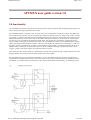
APVMUX user guide version 1.0
1.0 functionality
The APVMUX chip interfaces betwen the APV25 chip and the optical line driver chip, multiplexing the outputs of 2
APV25 chips onto a single optical line driver input.
The APVMUX chip has 4 channels, each consisting of a of 2-to-1 multiplexer as illustrated in Fig1. The differential
current outputs of the APV25 chips are converted into voltages by internal resistors as in Fig1. Each of these consists
of 8 resistors in parallel connected between each differential input and a reference voltage pad (one of these for each
differential input). Each resistor has a value of 400 Ohms. Switches (not shown) in series with each of these enable
the value of r to be varied between 400 Ohms and 50 Ohms. The switches are controlled by signals from an 8-bit
register loaded via the chip's I2c interface (see below). The two differential voltages are switched through to the chip
outputs alternately by the multiplexer switches. These are controlled by the outputs of the control logic (s1 and s2 in
the figure). When s1 is high the top switches are closed and the output of chip 1 is multiplexed through. When s2 is
high the bottom switches are closed and the output of chip 2 is multiplexed through. The functions of the "clock",
"trigger", "phase", and "mode" signals are explained in the next section.
Note that each of the switches shown is a complementary switch, each transistor having a width of 200 microns and a
length of 200nm. The resistance of each switch should be less than 2 Ohms.
The APVMUX chip also incorporates the TrackerPLL_IC chip. The details of this are not given here but may be
found in the documentation for that chip. Due to lack of space some pads are shared between the APVMUX and the
TrackerPLL_IC. Details of this are given below in the section entitled "Mux and TrackerPLL_IC addressing issues".
file://C:\WINNT\Profiles\mjf73\Desktop\apvmux-pll.html
12/15/00
Untitled Document
Page 2 of 11
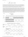
In the upper part of fig 2 (left) the initialisation procedure is shown. Signals s1 and s2 are internal and relate to the
state of the multiplexer as described above. Before initialisation the states of s1 and s2 are undefined. Initialisation
involves the application of the trigger sequence. A sequence of "1-0-1" is applied to the trigger input as shown. The
effect is that, exactly 4 positive clock edges after the start of the trigger sequence, s1 is in a high state and s2 is low.
Thus chip 1 is being read out at this point (assuming the "phase" and "mode" pads are unconnected).
The chip is provided with two pads used to vary the phasing of the multiplexer switching in relation to the output
signals of the two APV25 chips (chip1 and chip2). These are the "phase and "mode" pads. Their function is illustrated
in the lower part of fig2. With both phase and mode pads left unconnected, after initialisation the multiplexer samples
the output of each chip during the second half of the output's steady period, thus giving the output time to stabilize
before sampling. The effect of tying the phase pad low is to shift the phase of the sampling cycle by 180 degrees (see
fig2). This would be used if the chip output waveforms were swapped in relation to those shown. The function of the
mode pad is to advance the phase of the sampling cycle by 90 degrees so that sampling occurs in the the centre of the
output's steady period. This is achieved by tying the mode pad alone low. Finally this second mode of operation can
also be used with antiphase waveforms by tying both mode and phase pads low as shown in the figure. Note that the
mode and phase signals should not be changed after initialisation.
file://C:\WINNT\Profiles\mjf73\Desktop\apvmux-pll.html
12/15/00
Untitled Document
Page 3 of 11
2.0 Mux and TrackerPLL_IC addressing issues.
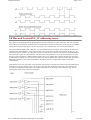
Fig 3 shows the pads shared between the multiplexer and the TrackerPLL_IC parts of the chip. The mux part of the
chip conforms to the usual I2c standard in that it is addressed by an 8-bit word, the first 7 bits being the chip address
and the last being the read/write bit. The PLL part requires only 5 address bits (see relevant documentation.
The four hardwired address pads, "addr_B<6:3>" are shared between the two parts. These represent the four most
significant bits of the addresses. These inputs are active low for the mux part and active high for the PLL part, so
inverters have been inserted to give the correct polarity for both parts (as shown). The next most significant address
bits of both parts (bit2) are tied internally to vdd. Since this is interpreted as a "0" by the mux part and a "1" by the
PLL part, each part requires a different address word to activate it. Address bits 1 and 0 of the mux part are tied to
ground. Hence if addr_B<6:3> are all tied to vdd, the mux will be addressed by: 0000011x and the PLL part will be
addressed by 00001xx. Since these words differ in the 5th bit position it is impossible to address both parts
simultaneously.
Note that the (active low) reset input resets both parts. Each part has a separate I2c interface. The serial data input is
common to the two I2c interfaces (the "sda_in" pad). The open drain serial data output pad is also common. It is
preceded by a multiplexer controlled by the "ENR" signal from the "VotedLogic" part of the PLL chip. The I2c
strobe signal "SCK" is also common to both parts.
file://C:\WINNT\Profiles\mjf73\Desktop\apvmux-pll.html
12/15/00
Untitled Document
Page 4 of 11
3.0 Physical Size and Pad Layout
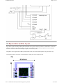
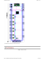
Fig 4 shows a plot of the chip with the pads numbered. The top part of the chip contains the TrackerPLL. In the lower
part is the multiplexer and associated logic. The pads at the top on the left are mainly outputs from the TrackerPLL.
The lower ones on the left are the multiplexer inputs (with reference pads).
The pads on the top right side are address pads plus the clock, reset and serial data pads for both parts of the chip.
The right hand pads at the bottom are the differential output pads of the multiplexer part.
file://C:\WINNT\Profiles\mjf73\Desktop\apvmux-pll.html
12/15/00
Untitled Document
Page 5 of 11
The dimensions of the chip are 2000x7100 microns.
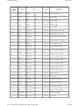
4.0 Pad Definition
Table 1. Definition of Pads
file://C:\WINNT\Profiles\mjf73\Desktop\apvmux-pll.html
12/15/00
Untitled Document
Page 6 of 11
Pad
Posistion
Name
Type
Value
Function
1
mode
pullup
-
see note
selects sample mode
2
vdd1
Power
-
see note
Positive Supply
3
vss1
power
-
see note
Negative supply
4
vss2
power
-
see note
Negative supply
5
vdd2
power
-
see note
Positive Supply
6
ckin -
LVDS i/p
-
see note
differential mux clock (neg)
7
ckin+
LVDS i.p
-
see note
differential mux clock (pos)
8
datin -
LVDS i/p
-
see note
differential mux reset inp(neg)
9
datin +
LVDS i/p
-
see note
differential mux reset inp(pos)
10
phase
pullup
-
see note
selects antiphase sampling
11
out6_7 -
analog o/p
-
see note
neg mux o/p (chips 6 and 7)
12
out6_7 +
analog o/p
-
see note
pos mux o/p (chips 6 and 7)
13
out4_5 -
analog o/p
-
see note
neg mux o/p (chips 4 and 5)
14
out4_5 +
analog o/p
-
see note
pos mux o/p (chips 4 and 5)
15
out2_3 -
analog o/p
-
see note
neg mux o/p (chips 2 and 3)
16
out2_3 +
analog o/p
-
see note
pos mux o/p (chips 2 and 3)
17
out0_1 -
analog o/p
-
see note
neg mux o/p (chips 0 and 1)
18
out0_1 +
analog o/p
-
see note
pos mux o/p (chips 0 and 1)
19
vss3
power
-
see note
Negative supply
20
vdd3
power
-
see note
Positive supply
21
sda_out
opendrain
-
see note
serial data out (both parts)
22
sda_in
hysteresis i/p
-
see note
serial data in (both parts)
23
sck
hysteresis i/p
-
see note
"SCL" input of PLL part
24
rstB
hysteresis i/p
-
see note
active low reset (both parts)
25
addressB<6>
hysteresis i/p
-
see note
MSB of chip address
26
addressB<5>
hysteresis i/p
-
see note
chip address
file://C:\WINNT\Profiles\mjf73\Desktop\apvmux-pll.html
12/15/00
Untitled Document
Page 7 of 11
27
addressB<4>
hysteresis i/p
-
see note
chip address
28
addressB<3>
hysteresis i/p
-
see note
chip address
29
clk_pll-
LVDS i/p
-
see note
"ClockAndT1" input of PLL(neg)
30
clk_pll+
LVDS i/p
-
see note
"ClockAndT1" input of PLL(pos)
31
unused1
unused
-
see note
-
32
unused2
unused
-
see note
-
33
vss4
power
-
see note
Negative supply
34
vdd4
power
-
see note
Positive supply
35
clk_out_0+
LVDS o/p
-
see note
clock o/p of PLL
36
clk_out_0-
LVDS o/p
-
see note
clock o/p of PLL
37
t1_0+
LVDS o/p
-
see note
trigger o/p of PLL
38
t1_0-
LVDS o/p
-
see note
trigger o/p of PLL
39
t1_1+
LVDS o/p
-
see note
trigger o/p of PLL
40
t1_1-
LVDS o/p
-
see note
trigger o/p of PLL
41
clk_out_1+
LVDS o/p
-
see note
clock o/p of PLL
42
clk_out_1-
LVDS o/p
-
see note
clock o/p of PLL
43
vdd5
power
-
see note
Positive supply
44
vss5
power
-
see note
Negative supply
45
in0+
analog i/p
-
see note
pos mux i/p (chip 0)
46
vref0
analog i/p
-
see note
mux ref i/p (chip 0)
47
in0-
analog i/p
-
see note
neg mux i/p (chip 0)
48
in1 -
analog i/p
-
see note
neg mux i/p (chip 1)
49
vref1
analog i/p
-
see note
mux ref i/p (chip 1)
50
in1 +
analog i/p
-
see note
pos mux i/p (chip 1)
51
in2 +
analog i/p
-
see note
pos mux i/p (chip 2)
52
vref2
analog i/p
-
see note
mux ref i/p (chip 2)
53
in2 -
analog i/p
-
see note
neg mux i/p (chip 2)
54
in3 -
analog i/p
-
see note
neg mux i/p (chip 3)
file://C:\WINNT\Profiles\mjf73\Desktop\apvmux-pll.html
12/15/00
Untitled Document
Page 8 of 11
55
vref3
analog i/p
-
see note
mux ref i/p (chip 3)
56
in3 +
analog i/p
-
see note
pos mux i/p (chip 3)
57
in4+
analog i/p
-
see note
pos mux i/p (chip 4)
58
vref4
analog i/p
-
see note
mux ref i/p (chip 4)
59
in4 -
analog i/p
-
see note
neg mux i/p (chip 4)
60
in5 -
analog i/p
-
see note
neg mux i/p (chip 5)
61
vref5
analog i/p
-
see note
mux ref i/p (chip 5)
62
in5 +
analog i/p
-
see note
pos mux i/p (chip 5)
63
in6 +
analog i/p
-
see note
pos mux i/p (chip 6)
64
vref6
analog i/p
-
see note
mux ref i/p (chip 6)
65
in6 -
analog i/p
-
see note
neg mux i/p (chip 6)
66
in7 -
analog i/p
-
see note
neg mux i/p (chip 7)
67
vref7
analog i/p
-
see note
mux ref i/p (chip 7)
68
in7 +
analog i/p
-
see note
pos mux i/p (chip 7)
4.1 pad definition notes
Pad of type :pullup - As detailed above, these must be left unconnected to obtain the default
functionality, but tied to vss to obtain alternate functionality.
power +/- 1.25V
LVDS i/p +/- 200mV (see table2 below)
analog o/p +/-1.25V
analog i/p +/-1.25V (note that the inputs should not exceed vdd or be less than vss)
hysteresis i/p - CMOS level inputs +/-1.25V with hysteresis to minimize noise effects.
opendrain - open drain N-type transistor output.
4.1.1 Low Voltage Differential Signal (LVDS)
These pads ("clock - & clock +"and "trig - & trig +") are used on those inputs that are
active during the sensitive acquisition time of the APV25 chip and are designed to
minimise interference in the latter.
file://C:\WINNT\Profiles\mjf73\Desktop\apvmux-pll.html
12/15/00
Untitled Document
Page 9 of 11
Table 2. Specification of LVDS Signal Levels
Parameter
Value
Offset Voltage
1.2V (above VSS)
Differential
Voltage
+/- 200mV
High Voltage
1.4V (above VSS)
Low Voltage
1.2V (above VSS)
The CMS Inner Tracker LVDS specification states that the signals are modulated on the
transmission media as a low amplitude differential signal (400mV). The transmission
media should be twisted pair cable with 100 Ohms characteristic impedance. The line
driver should be a constant current mode driver providing a 4mA output current to the
transmission media. The cable should be terminated to 100 Ohms at the receiving end,
where the terminating resistor converts the current into a voltage. The LVDS signal
should have a typical offset voltage of 1.2V above VSS and the receiver should tolerate
+/- 1V noise between the driver's VSS and the receiver's VSS.
Figure 5. LVDS point-to-point Connection
Figure 6. LVDS Signal Levels
file://C:\WINNT\Profiles\mjf73\Desktop\apvmux-pll.html
12/15/00
Untitled Document
Page 10 of 11
5.0 Running the APVMUX
Before powering up the chip ensure that the "phase" and "mode" pads are either tied to vss or floating as required (see
text next to fig 2). To initialise apply the trigger sequence using the trigger pads (again see text next to fig 2). Before
doing this it is desirable to load the set up the input resistors by loading the resistor register.
5.1 Loading the resistor register data.
Resistor register data is loaded via the I2c interface. It consists of an 8-bit word (see below) loaded as follows. After
the usual I2c 'start' signal, the first 7 bits presented to 'sda_in' are the chip address bits (see above). This is followed
by the read/write bit ( '0' for write and '1' for read ). After the acknowledge bit is output the next 7 bits are the register
address which is 0000011. this is followed by the read/write bit (same as above). After acknowledge the 8-bit data is
sent (see text for fig3). Thus the format for 'write' is:
start, chipaddr<6:0>, 0, ack, 0000011 0, ack, resistordata<7:0>, ack, stop
To read data back from the resistor register follow this sequence:
start, chipaddr<6:0>, 0, ack, 0000011 1, ack, stop
then follow with
start, chipaddr<6:0>, 1 ack, 0000011 1, ack, (resistordata<7:0> is output here) , (send ack to chip here), stop
5.2 Resistor register data.
The resistor register controls the value of the resistances (r) shown in Fig1. Section 1 details the resistor circuit and
values. A logic 1 loaded into the 8 bit resistor register corresponds to all the switches being closed and all the parallel
resistors carrying current. This corresponds to a resistance of about 50 Ohms. A logic 0 in any of the register bits
implies one of the switches being open. Loading only one logic 1 implies a resistance of 400 Ohms. The position of
this bit in the word is irrelevant. The data is loaded via the I2c serial data input using the usual I2c protocol (see
relevant documentation).
6.0 Additional features
The control logic of the multiplexer chip utilises specially designed flip-flops, each containing three conventional flipflops plus "majority vote" logic. If one of the flip-flops contains a different logic value from the others, this value is
not represented at the output. This system affords some immunity to single event upsets. See separate documentation
for the TrackerPLL_IC chip.
file://C:\WINNT\Profiles\mjf73\Desktop\apvmux-pll.html
12/15/00
Untitled Document
Page 11 of 11
P. Murray, 9th May 2000
file://C:\WINNT\Profiles\mjf73\Desktop\apvmux-pll.html
12/15/00