1
DisplayPort IP Core User Guide
Subscribe
Send Feedback
UG-01131
2015.05.04
101 Innovation Drive
San Jose, CA 95134
www.altera.com
TOC-2
Contents
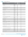
DisplayPort IP Core Quick Reference................................................................ 1-1
About This IP Core..............................................................................................2-1
Device Family Support................................................................................................................................ 2-2
IP Core Verification.....................................................................................................................................2-2
Performance and Resource Utilization.....................................................................................................2-2
Getting Started.................................................................................................... 3-1
Installing and Licensing IP Cores.............................................................................................................. 3-1
OpenCore Plus IP Evaluation........................................................................................................ 3-1
Specifying IP Core Parameters and Options............................................................................................3-2
Simulating the Design................................................................................................................................. 3-2
Simulating with the ModelSim Simulator.................................................................................... 3-3
Compiling the Full Design and Programming the FPGA......................................................................3-3
DisplayPort Source..............................................................................................4-1
Source Overview...........................................................................................................................................4-1
Source Functional Description.................................................................................................................. 4-2
Main Data Path.................................................................................................................................4-3
Embedded DisplayPort (eDP) Support.........................................................................................4-5
Source Parameters........................................................................................................................................4-5
Source Interfaces.......................................................................................................................................... 4-7
Controller Interface....................................................................................................................... 4-11
AUX Interface.................................................................................................................................4-12
Video Interface............................................................................................................................... 4-12
TX Transceiver Interface.............................................................................................................. 4-13
Transceiver Reconfiguration Interface....................................................................................... 4-14
Transceiver Analog Reconfiguration Interface..........................................................................4-14
Secondary Stream Interface..........................................................................................................4-14
Audio Interface...............................................................................................................................4-16
MSA Interface.................................................................................................................................4-18
Source Clock Tree......................................................................................................................................4-19
DisplayPort Sink..................................................................................................5-1
Sink Overview...............................................................................................................................................5-1
Sink Functional Description.......................................................................................................................5-1
Embedded DisplayPort (eDP) Support.........................................................................................5-4
Sink Parameters ...........................................................................................................................................5-4
Sink Interfaces.............................................................................................................................................. 5-6
Altera Corporation
TOC-3
Controller Interface....................................................................................................................... 5-13
AUX Interface.................................................................................................................................5-13
Debugging Interface...................................................................................................................... 5-14
Video Interface............................................................................................................................... 5-16
RX Transceiver Interface.............................................................................................................. 5-19
Transceiver Reconfiguration Interface....................................................................................... 5-19
Secondary Stream Interface..........................................................................................................5-19
Audio Interface...............................................................................................................................5-21
MSA Interface.................................................................................................................................5-22
Sink Clock Tree.......................................................................................................................................... 5-24
DisplayPort IP Core Hardware Demonstration.................................................6-1
Clock Recovery Core................................................................................................................................... 6-4
Clock Recovery Core Parameters.................................................................................................. 6-5
Clock Recovery Interface................................................................................................................ 6-6
Transceiver and Clocking......................................................................................................................... 6-11
Required Hardware................................................................................................................................... 6-14
Design Walkthrough................................................................................................................................. 6-22
Set Up the Hardware..................................................................................................................... 6-23
Copy the Design Files to Your Working Directory.................................................................. 6-23
Build the FPGA Design................................................................................................................. 6-25
Load, and Run the Software......................................................................................................... 6-25
View the Results............................................................................................................................. 6-26
DisplayPort IP Core Simulation Example.......................................................... 7-1
Design Walkthrough................................................................................................................................... 7-3
Copy the Simulation Files to Your Working Directory..............................................................7-3
Generate the IP Simulation Files and Scripts, and Compile and Simulate.............................. 7-6
View the Results............................................................................................................................... 7-8
DisplayPort API Reference................................................................................. 8-1
Using the Library......................................................................................................................................... 8-1
btc_dprx_syslib API Reference.................................................................................................................. 8-3
btc_dprx_aux_get_request......................................................................................................................... 8-3
btc_dprx_aux_handler................................................................................................................................ 8-4
btc_dprx_aux_post_reply........................................................................................................................... 8-5
btc_dprx_baseaddr...................................................................................................................................... 8-6
btc_dprx_dpcd_gpu_access........................................................................................................................8-6
btc_dprx_edid_set........................................................................................................................................8-7
btc_dprx_hpd_get........................................................................................................................................8-8
btc_dprx_hpd_pulse....................................................................................................................................8-8
btc_dprx_hpd_set........................................................................................................................................ 8-9
btc_dprx_syslib_add_rx..............................................................................................................................8-9
btc_dprx_syslib_info................................................................................................................................. 8-10
btc_dprx_syslib_init.................................................................................................................................. 8-11
btc_dprx_syslib_monitor..........................................................................................................................8-11
Altera Corporation
TOC-4
btc_dptx_syslib API Reference................................................................................................................ 8-12
btc_dptx_aux_i2c_read.............................................................................................................................8-12
btc_dptx_aux_i2c_write............................................................................................................................8-13
btc_dptx_aux_read.................................................................................................................................... 8-13
btc_dptx_aux_write...................................................................................................................................8-14
btc_dptx_baseaddr.....................................................................................................................................8-15
btc_dptx_edid_block_read....................................................................................................................... 8-15
btc_dptx_edid_read...................................................................................................................................8-16
btc_dptx_fast_link_training.....................................................................................................................8-16
btc_dptx_link_training............................................................................................................................. 8-17
btc_dptx_set_color_space.........................................................................................................................8-18
btc_dptx_syslib_init.................................................................................................................................. 8-18
btc_dptx_syslib_monitor..........................................................................................................................8-19
btc_dptx_test_autom.................................................................................................................................8-19
btc_dptx_video_enable............................................................................................................................. 8-20
btc_dpxx_syslib Additional Types.......................................................................................................... 8-20
btc_dprx_syslib Supported DPCD Locations........................................................................................ 8-20
DisplayPort Source Register Map and DPCD Locations................................... 9-1
Source General Registers.............................................................................................................................9-1
DPTX_TX_CONTROL...................................................................................................................9-1
DPTX_TX_STATUS....................................................................................................................... 9-3
Source MSA Registers..................................................................................................................................9-4
DPTX0_MSA_MVID......................................................................................................................9-4
DPTX0_MSA_NVID.......................................................................................................................9-4
DPTX0_MSA_HTOTAL................................................................................................................ 9-4
DPTX0_MSA_VTOTAL................................................................................................................ 9-5
DPTX0_MSA_HSP..........................................................................................................................9-5
DPTX0_MSA_HSW........................................................................................................................9-5
DPTX0_MSA_HSTART................................................................................................................. 9-6
DPTX0_MSA_VSTART................................................................................................................. 9-6
DPTX0_MSA_VSP.......................................................................................................................... 9-6
DPTX0_MSA_VSW........................................................................................................................ 9-7
DPTX0_MSA_HWIDTH............................................................................................................... 9-7
DPTX0_MSA_VHEIGHT.............................................................................................................. 9-7
DPTX0_MSA_MISC0..................................................................................................................... 9-8
DPTX0_MSA_MISC1..................................................................................................................... 9-8
DPTX0_MSA_COLOUR................................................................................................................9-8
Source Link Voltage and Pre-Emphasis Controls................................................................................... 9-9
DPTX_PRE_VOLT0........................................................................................................................9-9
DPTX_PRE_VOLT1..................................................................................................................... 9-10
DPTX_PRE_VOLT2..................................................................................................................... 9-10
DPTX_PRE_VOLT3..................................................................................................................... 9-10
DPTX_RECONFIG....................................................................................................................... 9-11
Source Timestamp..................................................................................................................................... 9-11
Source Audio Registers............................................................................................................................. 9-12
Source CRC Registers................................................................................................................................9-13
Source MST Registers................................................................................................................................9-14
Altera Corporation
TOC-5
DPTX_MST_VCPTAB0............................................................................................................... 9-15
DPTX_MST_VCPTAB1............................................................................................................... 9-15
DPTX_MST_VCPTAB2............................................................................................................... 9-16
DPTX_MST_VCPTAB3............................................................................................................... 9-17
DPTX_MST_VCPTAB4............................................................................................................... 9-17
DPTX_MST_VCPTAB5............................................................................................................... 9-18
DPTX_MST_VCPTAB6............................................................................................................... 9-18
DPTX_MST_VCPTAB7............................................................................................................... 9-19
DPTX_MST_TAVG_TS............................................................................................................... 9-20
Source AUX Controller Interface............................................................................................................ 9-20
DPTX_AUX_CONTROL............................................................................................................. 9-20
DPTX_AUX_CMD....................................................................................................................... 9-21
DPTX_AUX_BYTE0.....................................................................................................................9-22
DPTX_AUX_BYTE1.....................................................................................................................9-22
DPTX_AUX_BYTE2.....................................................................................................................9-22
DPTX_AUX_BYTE3.....................................................................................................................9-23
DPTX_AUX_BYTE4.....................................................................................................................9-23
DPTX_AUX_BYTE5.....................................................................................................................9-23
DPTX_AUX_BYTE6.....................................................................................................................9-24
DPTX_AUX_BYTE7.....................................................................................................................9-24
DPTX_AUX_BYTE8.....................................................................................................................9-24
DPTX_AUX_BYTE9.....................................................................................................................9-25
DPTX_AUX_BYTE10...................................................................................................................9-25
DPTX_AUX_BYTE11...................................................................................................................9-25
DPTX_AUX_BYTE12...................................................................................................................9-26
DPTX_AUX_BYTE13...................................................................................................................9-26
DPTX_AUX_BYTE14...................................................................................................................9-27
DPTX_AUX_BYTE15...................................................................................................................9-27
DPTX_AUX_BYTE16...................................................................................................................9-27
DPTX_AUX_BYTE17...................................................................................................................9-28
DPTX_AUX_BYTE18...................................................................................................................9-28
DPTX_AUX_RESET..................................................................................................................... 9-28
Source-Supported DPCD Locations....................................................................................................... 9-29
DisplayPort Sink Register Map and DPCD Locations..................................... 10-1
Sink General Registers...............................................................................................................................10-1
DPRX_RX_CONTROL.................................................................................................................10-1
DPRX_RX_STATUS..................................................................................................................... 10-3
DPRX_BER_CONTROL.............................................................................................................. 10-5
DPRX_BER_CNT0........................................................................................................................10-7
DPRX_BER_CNT1........................................................................................................................10-7
Sink Timestamp......................................................................................................................................... 10-7
Sink Bit-Error Counters............................................................................................................................10-7
DPRX_BER_CNTI0...................................................................................................................... 10-7
DPRX_BER_CNTI1...................................................................................................................... 10-8
Sink MSA Registers....................................................................................................................................10-8
DPRX0_MSA_MVID....................................................................................................................10-9
DPRX0_MSA_NVID.................................................................................................................... 10-9
Altera Corporation
TOC-6
DPRX0_MSA_HTOTAL.............................................................................................................. 10-9
DPRX0_MSA_VTOTAL.............................................................................................................. 10-9
DPRX0_MSA_HSP..................................................................................................................... 10-10
DPRX0_MSA_HSW....................................................................................................................10-10
DPRX0_MSA_HSTART.............................................................................................................10-10
DPRX0_MSA_VSTART............................................................................................................. 10-11
DPRX0_MSA_VSP......................................................................................................................10-11
DPRX0_MSA_VSW.................................................................................................................... 10-11
DPRX0_MSA_HWIDTH........................................................................................................... 10-12
DPRX0_MSA_VHEIGHT..........................................................................................................10-12
DPRX0_MSA_MISC0.................................................................................................................10-12
DPRX0_MSA_MISC1.................................................................................................................10-13
DPRX0_VBID.............................................................................................................................. 10-13
Sink Audio Registers............................................................................................................................... 10-14
DPRX0_AUD_MAUD................................................................................................................10-14
DPRX0_AUD_NAUD................................................................................................................ 10-14
DPRX0_AUD_AIF0.................................................................................................................... 10-14
DPRX0_AUD_AIF1.................................................................................................................... 10-15
DPRX0_AUD_AIF2.................................................................................................................... 10-15
DPRX0_AUD_AIF3.................................................................................................................... 10-15
DPRX0_AUD_AIF4.................................................................................................................... 10-16
Sink MST Registers..................................................................................................................................10-16
DPRX_MST_VCPTAB0............................................................................................................. 10-17
DPRX_MST_VCPTAB1............................................................................................................. 10-18
DPRX_MST_VCPTAB2............................................................................................................. 10-19
DPRX_MST_VCPTAB3............................................................................................................. 10-19
DPRX_MST_VCPTAB4............................................................................................................. 10-20
DPRX_MST_VCPTAB5............................................................................................................. 10-20
DPRX_MST_VCPTAB6............................................................................................................. 10-21
DPRX_MST_VCPTAB7............................................................................................................. 10-22
Sink AUX Controller Interface.............................................................................................................. 10-22
DPRX_AUX_CONTROL...........................................................................................................10-22
DPRX_AUX_STATUS................................................................................................................10-23
DPRX_AUX_COMMAND........................................................................................................10-24
DPRX_AUX_BYTE0...................................................................................................................10-24
DPRX_AUX_BYTE1...................................................................................................................10-25
DPRX_AUX_BYTE2...................................................................................................................10-25
DPRX_AUX_BYTE3...................................................................................................................10-25
DPRX_AUX_BYTE4...................................................................................................................10-26
DPRX_AUX_BYTE5...................................................................................................................10-26
DPRX_AUX_BYTE6...................................................................................................................10-26
DPRX_AUX_BYTE7...................................................................................................................10-27
DPRX_AUX_BYTE8...................................................................................................................10-27
DPRX_AUX_BYTE9...................................................................................................................10-27
DPRX_AUX_BYTE10.................................................................................................................10-28
DPRX_AUX_BYTE11.................................................................................................................10-28
DPRX_AUX_BYTE12.................................................................................................................10-29
DPRX_AUX_BYTE13.................................................................................................................10-29
DPRX_AUX_BYTE14.................................................................................................................10-29
Altera Corporation
TOC-7
DPRX_AUX_BYTE15.................................................................................................................10-30
DPRX_AUX_BYTE16.................................................................................................................10-30
DPRX_AUX_BYTE17.................................................................................................................10-30
DPRX_AUX_BYTE18.................................................................................................................10-31
DPRX_AUX_I2C0.......................................................................................................................10-31
DPRX_AUX_I2C1.......................................................................................................................10-31
DPRX_AUX_RESET...................................................................................................................10-32
DPRX_AUX_HPD...................................................................................................................... 10-32
Sink-Supported DPCD Locations......................................................................................................... 10-33
Additional Information......................................................................................A-1
Document Revision History...................................................................................................................... A-1
Altera Corporation
1
DisplayPort IP Core Quick Reference
2015.05.04
UG-01131
Subscribe
Send Feedback
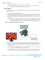
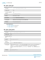
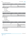
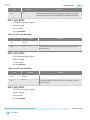
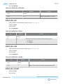
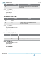
This document describes the Altera® DisplayPort MegaCore®function, which provides support for nextgeneration video display interface technology.
The DisplayPort IP core is part of the MegaCore IP Library, which is distributed with the Quartus® II
software and is downloadable from the Altera website at www.altera.com.
Note: For system requirements and installation instructions, refer to the Altera Software Installation and
Licensing Manual.
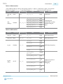
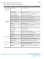
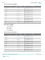
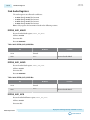
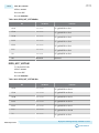
Item
Release Information
Description
Version
15.0
Release Date
May 2015
Ordering Code
IP-DP
Product ID
0109
Vendor ID
6AF7
© 2015 Altera Corporation. All rights reserved. ALTERA, ARRIA, CYCLONE, ENPIRION, MAX, MEGACORE, NIOS, QUARTUS and STRATIX words and logos are
trademarks of Altera Corporation and registered in the U.S. Patent and Trademark Office and in other countries. All other words and logos identified as
trademarks or service marks are the property of their respective holders as described at www.altera.com/common/legal.html. Altera warrants performance
of its semiconductor products to current specifications in accordance with Altera's standard warranty, but reserves the right to make changes to any
products and services at any time without notice. Altera assumes no responsibility or liability arising out of the application or use of any information,
product, or service described herein except as expressly agreed to in writing by Altera. Altera customers are advised to obtain the latest version of device
specifications before relying on any published information and before placing orders for products or services.
www.altera.com
101 Innovation Drive, San Jose, CA 95134
ISO
9001:2008
Registered
1-2
UG-01131
2015.05.04
DisplayPort IP Core Quick Reference
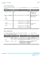
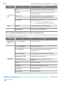
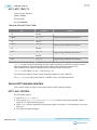
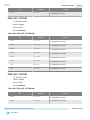
Item
Description
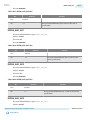
Core Features
• Conforms to the Video Electronics
Standards Association (VESA) specifica‐
tion version 1.2a
• Scalable main data link
• 1, 2, or 4 lane operation
• 1.62, 2.7, and 5.4 gigabits per second
(Gbps) per lane with an embedded
clock
• Color support
•
•
IP Core Information
•
•
•
• RGB 18, 24, 30, 36, or 48 bits per pixel
(bpp) color depths
• YCbCr 4:4:4 24, 30, 36, or 48 bpp color
depths
• YCbCr 4:2:2 16, 20, 24, or 32 bpp color
depths
40-bit (quad symbol) and 20-bit (dual
symbol) transceiver data interface
Support for 1, 2, or 4 parallel pixels per
clock
Multi-stream support (MST)
4Kp60 resolution support
Source
• Embedded controller AUX channel
operation
• Accepts standard H-sync/V-sync/data
enable RGB and YCbCr input video
formats
• Supports audio and video streams
• Sink
• Finite state machine (FSM) or
embedded controller AUX channel
operation
• Produces a proprietary video output
• Auxiliary channel for 2-way communica‐
tion (link and device management)
• Hot plug detect (HPD)
• Sink announces its presence
• Sink requests the source’s attention
• AC coupling and low EMI
Altera Corporation
DisplayPort IP Core Quick Reference
Send Feedback
UG-01131
2015.05.04
DisplayPort IP Core Quick Reference
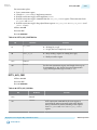
Item
1-3
Description
Typical Application
• Interfaces within a PC or monitor
• External display connections, including
interfaces between a PC and monitor or
projector, between a PC and TV, or
between a device such as a DVD player
and TV display
Device Family Support Arria® 10 (preliminary), Arria V GX, Arria V
GZ, Cyclone® V, and Stratix® V FPGA
devices.
Refer to the What’s New in Altera IP page of
the Altera website for detailed information.
Design Tools
• IP Catalog in the Quartus II software for
IP design instantiation and compilation
• TimeQuest timing analyzer in the
Quartus II software for timing analysis
• ModelSim-Altera software for design
simulation
Related Information
What’s New in Altera IP
DisplayPort IP Core Quick Reference
Send Feedback
Altera Corporation
About This IP Core
2
2015.05.04
UG-01131
Send Feedback
Subscribe
This document describes the Altera DisplayPort MegaCore function, which provides support for nextgeneration video display interface technology. The Video Electronics Standards Association (VESA)
defines the DisplayPort standard as an open digital communications interface for use in internal
connections such as:
®
®
• Interfaces within a PC or monitor
• External display connections, including interfaces between a PC and monitor or projector, between a
PC and TV, or between a device such as a DVD player and TV display
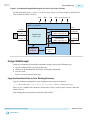
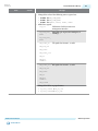
The Altera DisplayPort source has a scalable main link with 1, 2, or 4 lanes for a total up to 21.6 Gbps
bandwidth. A bidirectional AUX channel with 1 Mbps Manchester encoding provides side-band
communication. The sink uses a hot plug detect (HPD) signal to announce its presence, and the source
uses the same signal to initiate link configuration.
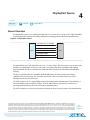
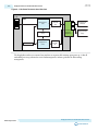
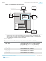
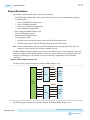
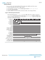
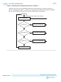
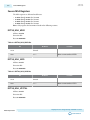
Figure 2-1: DisplayPort Source and Sink Communication
The main link has three selectable data rates: 1.62, 2.7, and 5.4 Gbps.
Source
Lane 0 Data (1.62, 2.7, or 5.4 Gbps)
Lane 1 Data (1.62, 2.7, or 5.4 Gbps)
Lane 2 Data (1.62, 2.7, or 5.4 Gbps)
Lane 3 Data (1.62, 2.7, or 5.4 Gbps)
AUX Channel (1 Mbps)
Hot Plug Detect
Sink
© 2015 Altera Corporation. All rights reserved. ALTERA, ARRIA, CYCLONE, ENPIRION, MAX, MEGACORE, NIOS, QUARTUS and STRATIX words and logos are
trademarks of Altera Corporation and registered in the U.S. Patent and Trademark Office and in other countries. All other words and logos identified as
trademarks or service marks are the property of their respective holders as described at www.altera.com/common/legal.html. Altera warrants performance
of its semiconductor products to current specifications in accordance with Altera's standard warranty, but reserves the right to make changes to any
products and services at any time without notice. Altera assumes no responsibility or liability arising out of the application or use of any information,
product, or service described herein except as expressly agreed to in writing by Altera. Altera customers are advised to obtain the latest version of device
specifications before relying on any published information and before placing orders for products or services.
www.altera.com
101 Innovation Drive, San Jose, CA 95134
ISO
9001:2008
Registered
2-2
UG-01131
2015.05.04
Device Family Support
Device Family Support
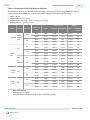
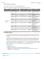
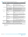
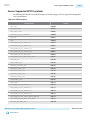
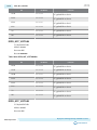
The following table lists the link rate support offered by the DisplayPort IP core for each Altera device
family.
Table 2-1: Link Rate Support by Device Family
RBR = Reduced Bit Rate, HBR = High Bit Rate
Device Family
20-bit mode
40-bit mode
Arria 10
RBR, HBR, HBR2
RBR, HBR, HBR2
Arria V GX
RBR, HBR
RBR, HBR, HBR2
Arria V GZ
RBR, HBR, HBR2
RBR, HBR, HBR2
Cyclone V
RBR, HBR
RBR, HBR
Stratix V
RBR, HBR, HBR2
RBR, HBR, HBR2
IP Core Verification
Before releasing a publicly available version of the DisplayPort IP core, Altera runs a comprehensive
®
verification suite in the current version of the Quartus II software. These tests use standalone methods
and the Qsys system integration tool to create the instance files. These files are tested in simulation and
hardware to confirm functionality. Altera tests and verifies the DisplayPort IP core in hardware for
different platforms and environments.
The DisplayPort IP core has been tested at VESA Plugtest events and passes the Unigraf DisplayPort Link
Layer CTS tests.
Performance and Resource Utilization
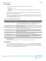
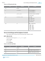
This section contains tables showing IP core variation size and performance examples.
The following table lists the resources and expected performance for selected variations. The results were
obtained using the Quartus II software v15.0 for the following devices:
•
•
•
•
Altera Corporation
Arria V (5AGXFB3H4F40C5)
Cyclone V (5CGTFD9E5F35C7)
Stratix V (5SGXEA7K2F40C2)
Arria 10 (10AX115S2F45I2SGES)
About This IP Core
Send Feedback
UG-01131
2015.05.04
2-3
Performance and Resource Utilization
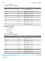
Table 2-2: DisplayPort IP Core FPGA Resource Utilization
The table below shows the resource information for Arria V and Cyclone V devices using M10K; Arria 10 and
Stratix V devices using M20K. The resources were obtained using the following parameter settings:
•
•
•
•
Mode = duplex
Maximum lane count = 4 lanes
Maximum video input color depth = 24 bits per pixel (bpp)
Pixel input mode = 1 pixel per clock
Device
Streams
Direction
Single
Arria 10 stream
(SST)
RX
TX
RX
SST
Arria V
GX
TX
MST
RX
(2
streams)
TX
Cyclone
SST
V GX
Stratix
V GX
RX
TX
RX
SST
TX
Logic Registers
Memory
Symbol per
Clock
ALMs
Primary
Secondary
Bits
M10K or
M20K
Dual
7,087
9,580
1,001
16,576
30
Quad
9,957
11,121
1,153
31,424
30
Dual
16,075
10,205
465
27,424
27
Quad
29,075
13,605
646
39,776
40
Dual
7,176
9,432
1,015
16,576
30
Quad
9,881
10,793
1,221
31,424
30
Dual
16,340
10,213
499
27,424
27
Quad
29,258
13,568
715
39,776
40
Dual
13,337
15,901
1,650
30,336
52
Quad
20,913
19,551
1,952
57,472
52
Dual
31,790
20,095
879
47,680
54
Quad
58,333
27,433
1,357
65,472
80
Dual
7,137
9,446
1,035
16,576
30
Quad
9,817
10,886
1,229
31,424
30
Dual
16,343
10,157
604
27,424
27
Quad
29,326
13,537
825
39,776
40
Dual
7,006
9,569
966
15,552
28
Quad
9,967
11,087
1,065
30,400
28
Dual
16,340
10,213
499
27,424
27
Quad
29,258
13,568
715
39,776
40
Related Information
Fitter Resources Reports
More information about Quartus II resource utilization reporting.
About This IP Core
Send Feedback
Altera Corporation
Getting Started
3
2015.05.04
UG-01131
Send Feedback
Subscribe
This chapter provides a general overview of the Altera IP core design flow to help you quickly get started
with the DisplayPort IP core. The IP core is installed as part of the Quartus II installation process. You can
select and parameterize any Altera IP core from the library. Altera provides an integrated parameter
editor that allows you to customize the DisplayPort IP core to support a wide variety of applications. The
parameter editor guides you through the setting of parameter values and selection of optional ports.
Installing and Licensing IP Cores
The Altera IP Library provides many useful IP core functions for your production use without purchasing
an additional license. Some Altera MegaCore IP functions require that you purchase a separate license for
production use. However, the OpenCore® feature allows evaluation of any Altera IP core in simulation
and compilation in the Quartus II software. After you are satisfied with functionality and perfformance,
visit the Self Service Licensing Center to obtain a license number for any Altera product.
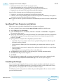
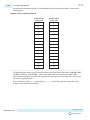
Figure 3-1: IP Core Installation Path
acds
quartus - Contains the Quartus II software
ip - Contains the Altera IP Library and third-party IP cores
altera - Contains the Altera IP Library source code
<IP core name> - Contains the IP core source files
Note: The default IP installation directory on Windows is <drive>:\altera\<version number>; on Linux it is
<home directory>/altera/ <version number>.
Related Information
• Altera Licensing Site
• Altera Software Installation and Licensing Manual
OpenCore Plus IP Evaluation
Altera's free OpenCore Plus feature allows you to evaluate licensed MegaCore IP cores in simulation and
hardware before purchase. You need only purchase a license for MegaCore IP cores if you decide to take
your design to production. OpenCore Plus supports the following evaluations:
© 2015 Altera Corporation. All rights reserved. ALTERA, ARRIA, CYCLONE, ENPIRION, MAX, MEGACORE, NIOS, QUARTUS and STRATIX words and logos are
trademarks of Altera Corporation and registered in the U.S. Patent and Trademark Office and in other countries. All other words and logos identified as
trademarks or service marks are the property of their respective holders as described at www.altera.com/common/legal.html. Altera warrants performance
of its semiconductor products to current specifications in accordance with Altera's standard warranty, but reserves the right to make changes to any
products and services at any time without notice. Altera assumes no responsibility or liability arising out of the application or use of any information,
product, or service described herein except as expressly agreed to in writing by Altera. Altera customers are advised to obtain the latest version of device
specifications before relying on any published information and before placing orders for products or services.
www.altera.com
101 Innovation Drive, San Jose, CA 95134
ISO
9001:2008
Registered
3-2
Specifying IP Core Parameters and Options
•
•
•
•
UG-01131
2015.05.04
Simulate the behavior of a licensed IP core in your system.
Verify the functionality, size, and speed of the IP core quickly and easily.
Generate time-limited device programming files for designs that include IP cores.
Program a device with your IP core and verify your design in hardware.
OpenCore Plus evaluation supports the following two operation modes:
• Untethered—run the design containing the licensed IP for a limited time.
• Tethered—run the design containing the licensed IP for a longer time or indefinitely. This requires a
connection between your board and the host computer.
Note: All IP cores that use OpenCore Plus time out simultaneously when any IP core in the design times
out.
Specifying IP Core Parameters and Options
Follow these steps to specify the DisplayPort IP core parameters and options.
1. Create a Quartus II project using the New Project Wizard available from the File menu.
2. On the Tools menu, click IP Catalog.
3. Under Installed IP, double-click Library > Interface > Protocols > Audio&Video > DisplayPort.
The parameter editor appears.
4. Specify a top-level name for your custom IP variation. This name identifies the IP core variation files
in your project. If prompted, also specify the targeted Altera device family and output file HDL
preference. Click OK.
5. Specify parameters and options in the DisplayPort parameter editor:
6.
7.
8.
9.
• Optionally select preset parameter values. Presets specify all initial parameter values for specific
applications (where provided).
• Specify parameters defining the IP core functionality, port configurations, and device-specific
features.
• Specify options for generation of a timing netlist, simulation model, testbench, or example design
(where applicable).
• Specify options for processing the IP core files in other EDA tools.
Click Generate to generate the IP core and supporting files, including simulation models.
Click Close when file generation completes.
Click Finish.
If you generate the DisplayPort IP core instance in a Quartus II project, you are prompted to add
Quartus II IP File (.qip) and Quartus II Simulation IP File (.sip) to the current Quartus II project.
Simulating the Design
You can simulate your DisplayPort IP core variation using the simulation model that the Quartus II
software generates. The simulation model files are generated in vendor-specific subdirectories of your
project directory. The DisplayPort IP core includes a simulation example.
The following sections teach you how to simulate the generated DisplayPort IP core variation with the
generated simulation model.
Altera Corporation
Getting Started
Send Feedback
UG-01131
2015.05.04
Simulating with the ModelSim Simulator
3-3
Related Information
DisplayPort IP Core Simulation Example on page 7-1
The Altera DisplayPort simulation example allows you to evaluate the functionality of the DisplayPort IP
Core and provides a starting point for you to create your own simulation. This example targets the
ModelSim SE simulator.
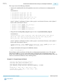
Simulating with the ModelSim Simulator
To simulate using the Mentor Graphics ModelSim simulator, perform the following steps:
1. Start the ModelSim simulator.
2. In ModelSim, change directory to the project simulation directory <variation>_sim/mentor.
3. Type the following commands to set up the required libraries and compile the generated simulation
model:
do msim_setup.tcl
ld
run -all
Compiling the Full Design and Programming the FPGA
You can use the Start Compilation command on the Processing menu in the Quartus II software to
compile your design. After successfully compiling your design, program the targeted Altera device with
the Programmer and verify the design in hardware.
Related Information
• Quartus II Incremental Compilation for Hierarchical and Team-Based Design
Provides more information about compiling the design.
• Quartus II Programmer
Provides more information about programming the device.
Getting Started
Send Feedback
Altera Corporation
DisplayPort Source
4
2015.05.04
UG-01131
Send Feedback
Subscribe
Source Overview
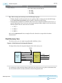
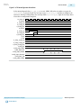
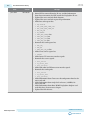
The DisplayPort source has a scalable main link with 1, 2, or 4 lanes for a total up to 21.6 Gbps bandwidth.
A bidirectional AUX channel with 1 Mbps Manchester encoding provides side-band communication.
Figure 4-1: DisplayPort Source
Source
Lane 0 Data (1.62, 2.7, or 5.4 Gbps)
Lane 1 Data (1.62, 2.7, or 5.4 Gbps)
Lane 2 Data (1.62, 2.7, or 5.4 Gbps)
Lane 3 Data (1.62, 2.7, or 5.4 Gbps)
AUX Channel (1 Mbps)
Hot Plug Detect
Sink
The main link has three selectable data rates: 1.62, 2.7, and 5.4 Gbps. The source device sets the lane count
and link rate combination (referred to as the policy) according to the sink’s capabilities and required
video bandwidth. The IP core transmits the video and audio streams on the main link with embedded
clocking.
The IP core transmits data in a scrambled ANSI 8B/10B format. The data transmission includes
redundancy for error detection. The secondary data stream, such as an audio stream, uses a ReedSolomon encoder for error correction.
The AUX channel is an AC-coupled differential pair for bidirectional communication. The signaling is a
self-clocked Manchester encoding at 1 Mbps. As in the 100-T Ethernet protocol, the encoder uses a
preceding synchronization pattern in each 16-byte maximum packet.
The AUX channel uses a master-slave hierarchy in which the source (master) initiates all communication.
© 2015 Altera Corporation. All rights reserved. ALTERA, ARRIA, CYCLONE, ENPIRION, MAX, MEGACORE, NIOS, QUARTUS and STRATIX words and logos are
trademarks of Altera Corporation and registered in the U.S. Patent and Trademark Office and in other countries. All other words and logos identified as
trademarks or service marks are the property of their respective holders as described at www.altera.com/common/legal.html. Altera warrants performance
of its semiconductor products to current specifications in accordance with Altera's standard warranty, but reserves the right to make changes to any
products and services at any time without notice. Altera assumes no responsibility or liability arising out of the application or use of any information,
product, or service described herein except as expressly agreed to in writing by Altera. Altera customers are advised to obtain the latest version of device
specifications before relying on any published information and before placing orders for products or services.
www.altera.com
101 Innovation Drive, San Jose, CA 95134
ISO
9001:2008
Registered
4-2
UG-01131
2015.05.04
Source Functional Description
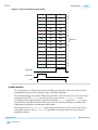
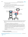
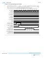
Source Functional Description
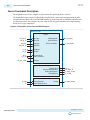
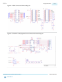
The DisplayPort source has a complete set of parameters for optimizing device resources.
The DisplayPort source consists of a DisplayPort encoder block, a transceiver management block, and a
controller interface block with an Avalon-MM interface for connecting with an embedded controller such
as a Nios II processor. You configure the ports using an RTL wrapper instantiation or by implementing
the IP core as a Qsys component.
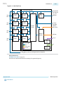
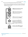
Figure 4-2: DisplayPort Source Top-Level Block Diagram
DisplayPort Source
Encoder
txN_video_in
txN_vid_clk
Video Input
Video Clock
AUX Debug Stream
(Avalon-ST Interface
txN_audio
txN_audio_clk
Audio Input
Audio Clock
TX Transceiver Interface
tx_aux
aux_clk
txN_ss
tx_ss_clk
txN_msa_conduit
tx_aux_debug
tx_xcvr_interface
AUX Interface
AUX Clock
Secondary Stream
(Avalon-ST Interface)
MSA Input
Transceiver Management
Calibration Clock
Transceiver Management Clock
TX Analog Reconfiguration
TX Reconfiguration
clk_cal
xcvr_mgmt_clk
tx_analog_reconfig
tx_reconfig
Controller Interface
tx_mgmt
clk
Altera Corporation
Avalon-MM Interface
Avalon-MM Interface Clock
Interrupt
tx_mgmt_interrupt
DisplayPort Source
Send Feedback
UG-01131
2015.05.04
Main Data Path
4-3
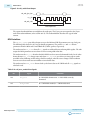
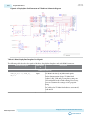
Figure 4-3: DisplayPort Source Functional Block Diagram
Fixed MSA
(txN_msa)
Multiplexer
Measure
Video
Legend
tx_ss_clk
clk
txN_vid_clk
aux_clk
txN_audio_clk
MSA
Generator
Throttle
Video Input
(txN_video_in)
Pixel
Steer
DCFIFO
Gearbox
FIFO
Blank Start
Generator
Audio Stream
(txN_audio)
Secondary Data
(txN_ss)
Audio
Encoder
Video Data
Packet
Generator
Secondary
Stream Encoder
Packetize
8B/10B
Encoder
40-Bit (Quad Symbol) or
20-Bit (Dual Symbol)
Data to Transceiver
DCFIFO
Training
Pattern 1
Training
Pattern 2
Avalon-MM
(tx_mgmt)
Controller
Registers
AUX
Controller
Bidirectional AUX Data
AUX Debug Stream
HPD
The source accepts a standard H-sync, V-sync, and data enable video stream for encoding. The IP core
latches and processes the video data before processing it using the txN_video_in input. N represents the
stream number: tx_video_in (Stream 0), tx1_video_in (Stream 1), tx2_video_in (Stream 2), and
tx3_video_in (Stream 3).
The video data width supports 6 to 16 bits per color (bpc) and is user selectable. If you set the Pixel input
mode option to Dual or Quad, the video input can accept two or four pixels per clock, thereby extending
the pixel clock rate capability.
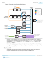
Main Data Path
The main data path consists of the packetizer, measurement, and blank generator paths. The IP core
multiplexes data from these three paths and outputs it through an 8B/10B encoder.
DisplayPort Source
Send Feedback
Altera Corporation
4-4
Packetizer Path
UG-01131
2015.05.04
Packetizer Path
The packetizer path provides video data resampling and packetization, and consists of the following steps:
1. The pixel steer block decimates the data to the requested lane count (1, 2, or 4).
2. The DCFIFO crosses the data into the main link clock domain (tx_ss_clk, generated by the
transceiver), which can be 270, 135, 81, 67.5, or 40.5 MHz depending on the actual main link rate
requested and the symbols per clock.
3. The gearbox resamples the video data according to the specified color depth. You can optimize the
gearbox by implementing fewer color depths. For example, you can reduce the resources required to
implement the system by supporting only the color depths you need instead of the complete set of
color depths specified in the DisplayPort specification.
4. The IP core packetizes the re-sampled data. The DisplayPort specification requires data to be sent in a
transfer unit (TU), which can be 32 to 64 link symbols long. To reduce complexity, the DisplayPort
source uses a fixed 64-symbol TU. The specification also requires that the video data be evenly distrib‐
uted within the TUs composing a full active video line. A throttle function distributes the data and
regulates it to ensure that the TUs leaving the IP core are evenly packed.
Note: A minimal DisplayPort system should support both 6 and 8 bpc. The VESA DisplayPort specifica‐
tion requires support for a mandatory VGA fail-safe mode (640 x 480 at 6 bpc).
The packetizer punctuates the outgoing 16-bit data stream with the correct packet comma codes.
Internally, the packetizer uses a symbol and a TU counter to ensure that it respects the TU boundaries.
Measurement Path
The measurement path determines the video geometry required for the DisplayPort main stream
attributes (MSA), which are sent once every vertical blanking interval. Optionally, the IP core can import
a fixed MSA data parameter from an external port, removing the measurement logic. This feature is useful
for embedded systems that only use known resolutions and synchronous pixel clocks.
Blank Generator Path
The blank generator path determines when to send the blank start comma codes with their corresponding
video data packets. This path can operate in enhanced or standard framing mode.
Multiplexer
The IP core multiplexes the packetized data, MSA data, and blank generator data into a single stream. The
combined data goes through 8B/10B encoding and is available as a 20-bit double-rate or a 40-bit quadrate DisplayPort encoded video port. The 20- or 40-bit port connects directly to the Altera high-speed
output transceiver.
During training periods, the source can send the DisplayPort clock recovery and symbol lock test patterns
(training pattern 1, training pattern 2, and training pattern 3, respectively), upon receiving the request
from downstream DisplayPort sink.
The source also implements an AUX channel controller, which you access using an embedded controller.
The embedded controller acts as an Avalon-MM master and sends read/write commands to the
Avalon-MM slave interface. The IP core clocks the AUX channel using a 16 MHz clock input (aux_clk).
Related Information
Controller Interface on page 4-11
Altera Corporation
DisplayPort Source
Send Feedback
UG-01131
2015.05.04
Embedded DisplayPort (eDP) Support
4-5
Embedded DisplayPort (eDP) Support
The DisplayPort IP core is compliant with eDP version 1.3. eDP is based on the VESA DisplayPort
standard. It has the same electrical interface and can share the same video port on the controller. The
DisplayPort IP core supports:
• Full (normal) link training—default
• Fast link training—mandatory eDP feature
Source Parameters
You set parameters for the source using the DisplayPort parameter editor.
Table 4-1: Source Parameters
Parameter
Description
Device family
Select the targeted device family—Arria 10, Arria V
GX, Arria V GZ, Cyclone V, or Stratix V—matches
the project device family.
Support DisplayPort source
Turn on to enable DisplayPort source.
Maximum video input color depth
Select the video input interface port bits per color.
Determines top-level video input port width (for
example, 6 bpc = 18 bpp, 16 bpc = 48 bpp).
TX maximum link rate
Select the the maximum link rate. 5.4 Gbps, 2.7
Gbps, 1.62 Gbps.
Note: Cyclone V devices do not support 5.4
Gbps.
Maximum lane count
Select the maximum lanes desired (1, 2, or 4).
Symbol output mode
Specify how many symbols are transferred during
each clock cycle: dual or quad symbol, or TX
transceiver data width: dual (20 bits) or quad (40
bits).
Dual symbol mode saves logic resource but requires
the core to run at twice the clock frequency of quad
symbol mode. If timing closure is a problem in the
device, you should consider using quad symbol
mode.
DisplayPort Source
Send Feedback
Altera Corporation
4-6
UG-01131
2015.05.04
Source Parameters
Parameter
Pixel input mode
Description
Select the number of pixels per clock (single, dual, or
quad symbol).
• If you select dual pixels per clock, the pixel clock
is ½ of the full rate clock and the video port
becomes two times wider.
• If you select four pixels per clock, the pixel clock
is ¼ of the full rate clock and the video port
becomes four times wider.
Scrambler seed value
Specify the initial seed for the scrambler block. Use
16’hFFFF for normal DP and 16’hFFFE for eDP.
Enable AUX debug stream
Turn on to send source AUX traffic output to an
Avalon-ST port.
Import fixed MSA
Turn on to enable the source to accept a fixed MSA
value from an external port.
Support CTS test automation
Turn on to support CTS test automation.
Support secondary data channel
Turn on to enable secondary data.
Support audio data channel
Turn on to enable audio packet encoding.
Note: To use this parameter, you must turn on
the Support secondary data channel
parameter.
Number of audio data channels
Specify the number of audio channels supported.
6-bpc RGB or YCbCr 4:4:4 (18 bpp)
Turn on to support 18 bpp encoding.
8-bpc RGB or YCbCr 4:4:4 (24 bpp)
Turn on to support 24 bpp encoding.
10-bpc RGB or YCbCr 4:4:4 (30 bpp)
Turn on to support 30 bpp encoding.
12-bpc RGB or YCbCr 4:4:4 (36 bpp)
Turn on to support 36 bpp encoding.
16-bpc RGB or YCbCr 4:4:4 (48 bpp)
Turn on to support 48 bpp decoding.
8-bpc YCbCr 4:2:2 (16 bpp)
Turn on to support 16 bpp encoding.
10-bpc YCbCr 4:2:2 (20 bpp)
Turn on to support 20 bpp encoding.
12-bpc YCbCr 4:2:2 (24 bpp)
Turn on to support 24 bpp encoding.
Altera Corporation
DisplayPort Source
Send Feedback
UG-01131
2015.05.04
Source Interfaces
Parameter
4-7
Description
16-bpc YCbCr 4:2:2 (32 bpp)
Turn on to support 32 bpp encoding.
Support MST
Turn on to enable multi-stream support.
Max stream count
Select the maximum amount of streams supported
(1-4).
Source Interfaces
The following tables list the source’s port interfaces. Your instantiation contains only the interfaces that
you have enabled.
Table 4-2: Controller Interface
Interface
Port Type
Clock Domain
Port
Direction
Description
clk
Clock
N/A
clk
Input
Clock for embedded
controller
reset
Reset
clk
reset
Input
Reset for embedded
controller
tx_mgmt_address[8:0]
Input
tx_mgmt_chipselect
Input
tx_mgmt_read
Input
tx_mgmt_write
Input
tx_mgmt
AV-MM
clk
tx_mgmt_
writedata[31:0]
tx_mgmt_readdata[31:0]
tx_mgmt_waitrequest
tx_mgmt_ IRQ
irq
DisplayPort Source
Send Feedback
clk
tx_mgmt_irq
Input
Avalon-MM interface
for embedded
controller
Outp
ut
Outp
ut
Output
Interrupt for
embedded controller
Altera Corporation
4-8
UG-01131
2015.05.04
Source Interfaces
Table 4-3: Transceiver Management Interface
n is the number of TX lanes.
Interface
Port Type
Clock Domain
Port
Direction
Description
xcvr_
Clock
mgmt_clk
N/A
xcvr_mgmt_clk
Input
Transceiver
management clock
clk_cal
N/A
clk_cal
Input
A 50-MHz calibration
clock input. This clock
must be synchronous
to the clock used for
the Transceiver
Reconfiguration block
(xvcr_mgmt_clk),
external to the Display‐
Port sink.
tx_vod[2n - 1:0]
Output
Clock
tx_emp[2n - 1:0]
tx_
analog_
reconfig
Conduit
xcvr_mgmt_
clk
tx_analog_reconfig_req
tx_analog_reconfig_ack
tx_analog_reconfig_
busy
tx_
reconfig
Conduit
xcvr_mgmt_
clk
Outp
ut
Outp
ut
Input
Transceiver analog
reconfiguration
handshaking
Input
tx_link_rate[1:0]
Output
tx_link_rate_
8bits[7:0]
Outp
ut
tx_reconfig_req
Input
tx_reconfig_ack
Input
tx_reconfig_busy
Input
Transceiver link rate
reconfiguration
handshaking
Note: Value of tx_link_rate[1:0]: 0=1.62Gbps, 1=2.70Gbps, 2=5.40Gbps; value of tx_link_rate_8bits[7:0]:
0×06=1.62Gbps, 0×0a=2.70Gbps, 0×14=5.40Gbps.
Note: For devices using a 50-MHz xcvr_mgmt_clk clock, connect the same clock directly also to the
clk_cal signal. For devices using a 100-MHz xcvr_mgmt_clk clock, connect the same clock to
clk_cal signal through a by-2 divider.
Altera Corporation
DisplayPort Source
Send Feedback
UG-01131
2015.05.04
Source Interfaces
4-9
Table 4-4: Video Interface
v is the number of bits per color, p is the pixels per clock (1 = single, 2 = dual, and 4 = quad). N is the stream
number; for example, tx_vid_clk represents Stream 0, tx1_vid_clk represents Stream 1, and so on.
Interface
txN_vid_
clk
txN_
video_in
Port Type
Clock
Conduit
Clock Domain
N/A
txN_vid_clk
Port
Direction
txN_vid_clk
Input
txN_vid_data[3v*p-1:0]
Input
txN_vid_v_sync[p-1:0]
Input
txN_vid_h_sync[p-1:0]
Input
txN_vid_f[p-1:0]
Input
txN_vid_de[p-1:0]
Input
Description
Video clock
Video data and
standard H/V synchro‐
nization video port
input
Table 4-5: AUX Interface
Interface
Port Type
Clock Domain
Port
Direction
Description
aux_clk
Clock
N/A
aux_clk
Input
AUX channel clock
aux_reset
Reset
aux_clk
aux_reset
Input
AUX channel reset
tx_aux_in
Input
tx_aux_out
tx_aux
Conduit
aux_clk
tx_aux_oe
tx_hpd
tx_aux_debug_
data[31:0]
tx_aux_debug_valid
tx_aux_debug_sop
tx_aux_
debug
AV-ST
aux_clk
tx_aux_debug_eop
tx_aux_debug_err
tx_aux_debug_cha
DisplayPort Source
Send Feedback
Outp
ut
Outp
ut
AUX channel interface
Input
Output
Outp
ut
Outp
ut
Outp
ut
Avalon-ST stream of
AUX data for
debugging
Outp
ut
Outp
ut
Altera Corporation
4-10
UG-01131
2015.05.04
Source Interfaces
Table 4-6: Secondary Interface
N is the stream number; for example, tx_msa_conduit represents Stream 0, tx1_msa_conduit represents Stream
1, and so on.
Interface
Signal Type
Clock Domain
Port
Direction
Description
tx_ss_clk
Clock
N/A
tx_ss_clk
Output
TX transceiver clock
out and clock for
secondary stream
MSA
Conduit
tx_ss_clk
txN_msa[191:0]
Input
Input port for fixed
MSA parameters
txN_ss_data[127:0]
Input
txN_ss_valid
Input
(txN_
msa_
conduit)
Secondary
Stream
AV-ST
(txN_ss)
tx_ss_clk
Outp
ut
txN_ss_ready
txN_ss_sop
Input
txN_ss_eop
Input
Secondary stream
interface
Table 4-7: Audio Interface
m is the number of TX audio channels. N is the stream number; for example, tx_audio represents Stream 0,
tx1_audio represents Stream 1, and so on.
Interface
Signal Type
Clock
Clock
Domain
N/A
Audio
(txN_audio)
Altera Corporation
Conduit
txN_audio_
clk
Port
txN_audio_clk
txN_audio_lpcm_data
[m*32-1:0]
Direction
Input
Description
Audio clock
Input
txN_audio_valid
Input
txN_audio_mute
Input
Audio sample data
interface
DisplayPort Source
Send Feedback
UG-01131
2015.05.04
Controller Interface
4-11
Table 4-8: TX Transceiver Interface
n is the number of TX lanes, s is the number of symbols per clock.
Note: Connect the DisplayPort signals to the Native PHY signals of the same name.
Interface
Port Type
Clock
Conduit
Conduit
Conduit
TX transceiver
interface
Clock
Domain
Port
N/A
tx_std_clkout[n–1:0]
tx_std_
clkout
tx_parallel_
data[n*s*10–1:0]
N/A
tx_pll_powerdown
xcvr_mgmt_
clk
tx_digitalreset[n–
1:0]
Direction
Description
Input
TX transceiver clock
out
Output
Parallel data for TX
transceiver
Output
PLL power down for
TX transceiver
Output
Resets the digital TX
portion of TX
transceiver
Output
Resets the analog TX
portion of TX
transceiver
Conduit
N/A
Conduit
N/A
tx_cal_busy[n–1:0]
Input
Calibration in
progress signal from
TX transceiver
Conduit
N/A
tx_pll_locked
Input
PLL locked signal
from TX transceiver
tx_analogreset[n–
1:0]
Controller Interface
The controller interface allows you to control the source from an external or on-chip controller, such as
the Nios II processor. The controller can control the DisplayPort link parameters and the AUX channel
controller.
The AUX channel controller interface works with a simple serial-port-type peripheral that operates in a
polled mode. Because the DisplayPort AUX protocol is a master-slave interface, the DisplayPort source
(the master) starts a transaction by sending a request and then waits for a reply from the attached sink.
The controller interface includes a single interrupt source. The interrupt notifies the controller of an HPD
signal state change. Your system can interrogate the DP_TX_STATUS register to determine the cause of the
interrupt. Writing to the DP_TX_STATUS register clears the pending interrupt event.
Related Information
• Multiplexer on page 4-4
• DisplayPort Source Register Map and DPCD Locations on page 9-1
DisplayPort source instantiations require an embedded controller (Nios II processor or another
controller) to act as the policy maker.
DisplayPort Source
Send Feedback
Altera Corporation
4-12
UG-01131
2015.05.04
AUX Interface
AUX Interface
The IP core has three ports that control the serial data across the AUX channel:
• Data input (tx_aux_in)
• Data output (tx_aux_out)
• Output enable (tx_aux_oe). The output enable port controls the direction of data across the bidirec‐
tional link.
These ports are clocked by the source’s 16 MHz clock (aux_clk). The AUX channel’s physical layer is a
bidirectional 2.5 V SSTL Class II interface.
The source’s AUX controller allows you to capture all bytes sent from and received by the AUX channel,
which is useful for debugging. The IP core provides a standard stream interface that you can use to drive
an Avalon-ST FIFO component directly.
Table 4-9: Source AUX Debug Interface Ports
Port
Comments
tx_aux_debug_data[31:0]
The source AUX debug interface inserts a 1 µs timestamp counter in bits
[31:8]; bits [7:0] represent the byte received or transmitted.
tx_aux_debug_valid
Qualifies valid stream data.
tx_aux_debug_sop
Indicates the message packet’s first byte.
tx_aux_debug_eop
Indicates the message packet’s last byte. The last byte should be ignored
and is not part of the message.
tx_aux_debug_err
Indicates if the IP core detects an error in the current byte.
tx_aux_debug_cha
Indicates the direction of the current byte. 1 = byte transmitted by the
source, 0 = byte received from the sink.
Related Information
AN 522: Implementing Bus LVDS Interface in Supported Altera Device Families
Video Interface
The core sends video to be encoded through the txN_video_in interface, which provides a standard Hsync and V-sync input with support for interlaced or progressive video. You specify the data input width
via a parameter. The same input port transfers RGB and YCbCr data in either 4:4:4 or 4:2:2 color format.
Data is most-significant bit aligned and formatted for 4:4:4.
Altera Corporation
DisplayPort Source
Send Feedback
UG-01131
2015.05.04
TX Transceiver Interface
4-13
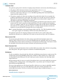
Figure 4-4: Video Input Data Format
18 bpp to 48 bpp port width when txN_video_in port width is 48 (16 bpc, 1 pixel per clock)
18 bpp RGB
24 bpp RGB/YCBCr444 (8 bpc)
30 bpp RGB/YCBCr444 (10 bpc)
36 bpp RGB/YCBCr444 (12 bpc)
48 bpp RGB/YCBCr444 (16 bpc)
47
32
31
16
15
0
txN_vid_data[47:0]
The following figure shows the sub-sampled 4:2:2 color format for a video port width of n. The mostsignificant half of the video port always transfers the Y component while the least-significant half of the
video port transfers the alternate Cr or Cb component. If the Y/Cb/Cr component widths are less than
n/2, they must be most-significant bit aligned with respect to the n and n/2-1 boundaries.
Figure 4-5: Sub-Sampled 4:2:2 Color Format Video Port
n-1
n/2 n/2-1
0
txN_vid_data[n - 1:0]
If you set the Pixel input mode option to Dual or Quad, the IP core sends two or four pixels in parallel,
respectively. To support video resolutions with horizontal active, front porch or back porch of a length
not divisible by 2 or 4, the following signals are widened:
• Horizontal and vertical syncs
• Data enable
The following figure shows the pixel data order from least significant bits to most significant bits.
Figure 4-6: Video Input Data Alignment
For RGB 18 bpp when txN_video_in port width is 96 (8 bpc, 4 pixels per clock)
95
72
Pixel 3
71
48
Pixel 2
47
24
Pixel 1
23
0
txN_vid_data[95:0]
Pixel 0
TX Transceiver Interface
The transceiver or Native PHY IP core instance is no longer instantiated within the DisplayPort IP core.
The DisplayPort IP uses a soft 8B/10B encoder. This interface provides TX encoded video data
(tx_parallel_data) in either dual symbol (20-bit) or quad symbol (40-bit) mode and drives the digital
DisplayPort Source
Send Feedback
Altera Corporation
4-14
UG-01131
2015.05.04
Transceiver Reconfiguration Interface
reset (tx_digitalreset), analog reset (tx_analogreset), and PLL powerdown signals
(tx_pll_powerdown) of the transceiver.
Transceiver Reconfiguration Interface
You can reconfigure the transceiver to accept single reference clock. The single reference clock is a 135MHz clock for all bit rates: RBR, HBR, and HBR2.
• During run-time, you can reconfigure the transceiver to operate in either one of the bit rate by
changing TX CMU PLL divide ratio.
When the IP core makes a request, the tx_reconfig_req port goes high. The user logic asserts
tx_reconfig_ack and then reconfigures the transceiver. During reconfiguration, the user logic holds
tx_reconfig_busy high. The user logic drives it low when reconfiguration completes.
Note: The transceiver requires a reconfiguration controller. Reset the transceiver to a default state upon
power-up.
Related Information
• AN 645: Dynamic Reconfiguration of PMA Controls in Stratix V Devices
Provides more information about using the Transceiver Reconfiguration Controller to reconfigure the
Stratix V Physical Media Attachment (PMA) controls dynamically.
• Altera Transceiver PHY IP Core User Guide
Provides more information about how to reconfigure the transceiver for 28-nm devices.
• AN 676: Using the Transceiver Reconfiguration Controller for Dynamic Reconfiguration in
Arria V and Cyclone V Devices
Provides more information about using the Transceiver Reconfiguration Controller to reconfigure the
Arria V Physical Media Attachment (PMA) controls dynamically.
• AN 678: High-Speed Link Tuning Using Signal Conditioning Circuitry
Provides more information about link tuning.
• Arria 10 Transceiver PHY User Guide
Provides more information about how to reconfigure the transceiver for Arria 10 devices.
Transceiver Analog Reconfiguration Interface
The tx_analog_reconfig interface uses the tx_vod and tx_emp transceiver management control ports.
You must map these ports for the device you are using. To change these values, the core drives
tx_analog_reconfig_req high. Then, the user logic sets tx_analog_reconfig_ack high to acknowledge
and drives tx_analog_reconfig_busy high during reconfiguration. When reconfiguration completes,
the user logic drives tx_analog_reconfig_busy low.
Secondary Stream Interface
You can transmit the secondary stream data over the DisplayPort main link through the secondary stream
(txN_ss) interface. This interface uses handshaking and back pressure to control packet delivery.
Internally, the core uses a FIFO to store packets until a slot becomes available on the main link. If the
FIFO fills up, the secondary stream interface stops accepting packets and applies back pressure. The
packet must be available at the time of sending because the txN_ss port does not support forward
pressure.
Altera Corporation
DisplayPort Source
Send Feedback
UG-01131
2015.05.04
Secondary Stream Interface
4-15
The txN_ss interface input data format corresponds to four, 15-nibble code words as specified by the
DisplayPort version 1.2a specification section 2.2.6.3. The upstream Reed-Solomon encoder supplies these
15-nibble code words. The format differs for header and payload as shown in the following figure.
Figure 4-7: Secondary Stream Input Data Format
15-Nibble Code Word
for Packet Payload
15-Nibble Code Word
for Packet Header
0
0
0
0
0
0
0
0
0
0
nb0
0
nb1
0
nb2
0
nb3
0
nb4
0
nb5
0
nb6
nb0
nb7
nb1
p0
p0
p1
p1
The following figure shows a typical secondary stream packet with a four-byte header (HB0, HB1, HB2
and HB3) and a 32-byte payload (DB0 … DB31). The core calculates the associated parity bytes. The
secondary stream interface uses the start-of-packet (SOP) and end-of-packet (EOP) to determine if the
current input is a header or payload.
Payloads that only contain the first 16 bytes can assert the EOP on the second cycle to terminate the
packet sequence. Data is clocked in to the secondary stream interface through the tx_ss_clk. This clock
is the same phase and frequency as the main-link lane 0 clock.
DisplayPort Source
Send Feedback
Altera Corporation
4-16
UG-01131
2015.05.04
Audio Interface
Figure 4-8: Typical Secondary Stream Packet
0
DB15
DB31
0
DB14
DB30
0
DB13
DB29
HB3
DB12
DB28
0
DB11
DB27
0
DB10
DB26
0
DB9
DB25
HB2
DB8
DB24
0
DB7
DB23
0
DB6
DB22
0
DB5
DB21
HB1
DB4
DB20
0
DB3
DB19
0
DB2
DB18
0
DB1
DB17
HB0
DB0
DB16
Data[127:0]
End of Packet
Start of Packet
Valid
Audio Interface
The audio encoder is upstream of the secondary stream encoder. It generates the Audio InfoFrame,
Timestamp, and Audio sample packets from the incoming audio sample data stream. Then, it sends the
three packet types to the secondary stream encoder before they are transmitted to the downstream sink
device.
The audio port is parameterized for the number of audio channels required in the design. You can use 2
or 8 channels. Each channel’s audio data is sent to the txN_audio_lpcm_data port.
The IP core requires a txN_audio_valid signal for designs in which the txN_audio_clk signal is higher
than the actual sample clock. The txN_audio_valid signal qualifies the audio data on the
txN_audio_lpcm_data input.
Altera Corporation
DisplayPort Source
Send Feedback
UG-01131
2015.05.04
4-17
Audio Interface
Table 4-10: Audio Signals
Signal
Comments
txN_audio_clk
Audio interface input clock.
txN_audio_valid
Audio input data valid.
txN_audio_mute
When asserted, indicates that audio muting is enabled.
txN_audio_lpcm_data[m*321:0]
m-channel, 32-bit audio sample data.
Figure 4-9: Audio Sample Data Bits
The packing format uses an IEC-60958-type encoding.
31
24 23
7
B3
0 7
16 15
B2
0 7
8 7
B1
0 7
31 30 29 28 27 26 25 24 23
SP R
PR
P C
0
B0
0
0
U V MSB
Audio Sample Word [23:0]
LSB
Table 4-11: Audio Sample Bit Field Definitions
Bit Name
Bit Position
Audio sample Byte 2, bits 7:0
word
Byte 1, bits 7:0
Description
Byte 0, bits 7:0
Audio data. The data content depends on the audio coding type. For
LPCM audio, the audio most significant bit (MSB) is placed in byte
2, bit 7. If the audio data size is less than 24 bits, unused least signifi‐
cant bits (LSB) must be zero padded.
V
Byte 3, bit 0
Validity flag.
U
Byte 3, bit 1
User bit.
C
Byte 3, bit 2
Channel status.
P
Byte 3, bit 3
Parity bit.
PR
Byte 3, bits 4 - 5
Preamble code and its correspondence with IEC-60958 preamble:
00: Subframe 1 and start of the audio block (11101000 preamble)
01: Subframe1 (1110010 preamble)
10: Subframe 2 (1110100 preamble)
R
DisplayPort Source
Send Feedback
Byte3, bit 6
Reserved bit; must be 0.
Altera Corporation
4-18
UG-01131
2015.05.04
MSA Interface
Bit Name
Bit Position
SP
Byte 3, bit 7
Description
Sample present bit:
1: Sample information is present and can be processed.
0: Sample information is not present.
All one-sample channels, used or unused, must have the same
sample present bit value.
This bit is useful for situations in which 2-channel audio is
transported over a 4-lane main link. In this operation, main link
lanes 2 and 3 may or may not have the audio sample data. This bit
indicates whether the audio sample is present or not.
The source automatically generates the Audio InfoFrame and fills it with only information about the
number of channels used. Use the audio channel status to provide any information about the audio
stream needed by downstream devices.
MSA Interface
For applications that use a known video source signal, you can remove the added resource of video
measurement. In this scenario, the DisplayPort source uses the MSA values presented on the
txN_msa_conduit signal bundle shown below:
wire [191:0] txN_msa_conduit = {Mvid[23:0], Nvid[23:0], Htotal[15:0], Vtotal[15:0],
HSP, HSW[14:0], Hstart[15:0],
Vstart[15:0], VSP, VSW[14:0], Hwidth[15:0], Vheight[15:0], MISC0[7:0], MISC1[7:0]};
Table 4-12: txN_msa_conduit Port Signals
Bit
Signal
Comments
Mvid for the main video stream. Used for stream clock recovery
from link symbol clock.
191:168
Mvid[23:0]
167:144
Nvid[23:0]
143:128
Htotal[15:0]
Horizontal total of received video stream in pixels
127:112
Vtotal[15:0]
Vertical total of received video stream in lines
111
HSP
H-sync polarity 0 = Active high, 1 = Active low
110:96
HSW[14:0]
H-sync width in pixels
95:80
Hstart[15:0]
Altera Corporation
Nvid for the main video stream. Used for stream clock recovery
from link symbol clock.
Horizontal active start from H-sync start in pixels (H-sync width
+ Horizontal back porch)
DisplayPort Source
Send Feedback
UG-01131
2015.05.04
Source Clock Tree
Bit
Signal
4-19
Comments
Vertical active start from V-sync start in lines (V-sync width +
Vertical back porch)
79:64
Vstart[15:0]
63
VSP
V-sync polarity 0 = Active high, 1 = Active low
62:48
VSW[14:0]
V-sync width in lines
47:32
Hwidth[15:0]
Active video width in pixels
31:16
Vheight[15:0]
Active video height in lines
15:8
MISC0[7:0]
7:0
MISC1[7:0]
The MISC0[7:1] and MISC1[7] fields indicate the color encoding
format. The color depth is indicated in MISC0[7:5]:
•
•
•
•
•
000 - 6 bpc
001 - 8 bpc
010 - 10 bpc
011 - 12 bpc
100 - 16 bpc
For details about the encoding format, refer to the DisplayPort
v1.2 specification.
Source Clock Tree
The source uses the following clocks:
• Local pixel clock (txN_vid_clk), which clocks video data into the IP core.
• Main link clock (tx_ss_clk), which clocks data out of the IP core and into the high-speed serial
output (HSSI) components. The main link clock is the output of the CMU PLL clock. You can supply
the CMU PLL with the single reference clock (135 MHz). You can use other frequencies by changing
the CMU PLL divider ratios and/or reconfiguring the transceiver. The 20- or 40- bit data fed to the
HSSI is synchronized to a single HSSI[0] clock. If you select the dual symbol mode option, this clock is
equal to the link rate divided by 20 (270, 135, or 81 MHz). If you turn on quad symbol mode, this clock
is equal to the link rate divided by 40 (135, 67.5, or 40.5 MHz).
• 16 MHz clock (aux_clk), which the IP core requires to encode or decode the AUX channel. A separate
clock (clk) clocks the Avalon-MM interface.
• txN_audio_clk for the audio interface.
DisplayPort Source
Send Feedback
Altera Corporation
4-20
UG-01131
2015.05.04
Source Clock Tree
Figure 4-10: Source Clock Tree
Recovered Clock
from Transceiver
(tx_ss_clk)
Audio Clock
(txN_audio_clk)
Audio Data
DisplayPort Encoder
Front-End
Audio FIFO
Secondary
Stream Data
270/135/81/67.5/40.5 MHz
Transceiver Block
Audio
Encoder
Sync
HSSIO0
Main
Link 0
Secondary
Stream
Encoder
Sync
HSSIO1
Main
Link 1
Sync
HSSIO2
Main
Link 2
Sync
HSSIO3
Main
Link 3
Back-End
Encoder
Pixel Clock
(txN_vid_clk)
Front-End
Video FIFO
Video Data
aux_clk
AUX
Controller
clk
Controller
Interface
Legend
tx_ss_clk
clk
txN_vid_clk
aux_clk
txN_audio_clk
CMU PLL
Transceiver Reference Clock Signal(s) from PLL or Dedicated Pin } 135 MHz
Altera Corporation
DisplayPort Source
Send Feedback
DisplayPort Sink
5
2015.05.04
UG-01131
Send Feedback
Subscribe
Sink Overview
The DisplayPort sink has a scalable main link with 1, 2, or 4 lanes for a total up to 21.6 Gbps bandwidth. A
bidirectional AUX channel with 1 Mbps Manchester encoding provides side-band communication. The
sink drives a hot plug detect (HPD) signal to notify the source that a sink is present. Additionally, it
provides an interrupt mechanism so that the sink can get the source’s attention.
Figure 5-1: DisplayPort Sink Block Diagram
Source
Lane 0 Data (1.62, 2.7, or 5.4 Gbps)
Lane 1 Data (1.62, 2.7, or 5.4 Gbps)
Lane 2 Data (1.62, 2.7, or 5.4 Gbps)
Lane 3 Data (1.62, 2.7, or 5.4 Gbps)
AUX Channel (1 Mbps)
Hot Plug Detect
Sink
The main link has three selectable data rates: 1.62, 2.7, and 5.4 Gbps. The source device sets the lane count
and link rate combination (referred to as the policy) according to the sink’s capabilities and required
video bandwidth.
The AUX channel is an AC-coupled differential pair for bidirectional communication. The signaling is a
self-clocked Manchester encoding at 1 Mbps. Like 100-T Ethernet, the encoder uses a preceding synchro‐
nization pattern in each 16-byte maximum packet. The AUX channel uses a master/slave hierarchy in
which the source (master) initiates all communication.
Sink Functional Description
The DisplayPort sink has a complete set of parameters for optimizing device resources.
The DisplayPort sink consists of a DisplayPort decoder block, a transceiver management block, and a
controller interface block with an Avalon-MM interface for connecting with an embedded controller such
as the Nios II processor. You can configure the ports using an RTL wrapper instantiation or
implementing the IP core as a Qsys component.
© 2015 Altera Corporation. All rights reserved. ALTERA, ARRIA, CYCLONE, ENPIRION, MAX, MEGACORE, NIOS, QUARTUS and STRATIX words and logos are
trademarks of Altera Corporation and registered in the U.S. Patent and Trademark Office and in other countries. All other words and logos identified as
trademarks or service marks are the property of their respective holders as described at www.altera.com/common/legal.html. Altera warrants performance
of its semiconductor products to current specifications in accordance with Altera's standard warranty, but reserves the right to make changes to any
products and services at any time without notice. Altera assumes no responsibility or liability arising out of the application or use of any information,
product, or service described herein except as expressly agreed to in writing by Altera. Altera customers are advised to obtain the latest version of device
specifications before relying on any published information and before placing orders for products or services.
www.altera.com
101 Innovation Drive, San Jose, CA 95134
ISO
9001:2008
Registered
5-2
UG-01131
2015.05.04
Sink Functional Description
Figure 5-2: DisplayPort Sink Top-Level Block Diagram
DisplayPort Sink
Decoder
Secondary Stream
(Avalon-ST Interface)
rxN_ss
rxN_ss_clk
Audio Output
rxN_audio
Video Output
Video Clock
rxN_video_out
rxN_vid_clk
MSA Output
Stream Debug
rxN_stream
AUX Interface
AUX Clock
rx_aux
aux_clk
Link Parameters
rx_edid
rx_xcvr_interface
EDID Interface
RX Transceiver Interface
rxN_msa_conduit
AUX Debug Stream
(Avalon-ST Interface)
rx_params
rx_aux_debug
Transceiver Management
Calibration Clock
Transceiver Management Clock
RX Reconfiguration
clk_cal
xcvr_mgmt_clk
rx_reconfig
Controller Interface
rx_mgmt
clk
Altera Corporation
Avalon-MM Interface
Avalon-MM Interface Clock
Interrupt
rx_mgmt_interrupt
DisplayPort Sink
Send Feedback
UG-01131
2015.05.04
Sink Functional Description
5-3
Figure 5-3: DisplayPort Sink Functional Block Diagram
IRQ
Control
HPD
SS
Decoder
20-Bit (Dual Symbol)
or 40-Bit (Quad Symbol)
Data from Transceiver
(rx_xcvr_interface)
8B/10B
Aligner
Deskew
De-Scrambler
DP2ST
DCFIFO
Gearbox
VB-ID
Decoder
MSA
Decoder
Bidirectional AUX Data (rx_aux)
HPD
AUX
Controller
Controller Registers
DCFIFO
Secondary
Stream (rxN_ss)
Steering
Video Output
(rxN_video_out)
Legend
rx_ss_clk
clk
rxN_vid_clk
aux_clk
Avalon-MM (rx_mgmt)
AUX Debug Stream (rx_aux_debug)
The device transceiver sends 20-bit (dual symbol) or 40-bit (quad symbol) parallel DisplayPort data to the
sink. Each data lane is clocked in to the IP core by its own respective clock output from the transceiver.
Inside the sink, the four independent clock domains are synchronized to the lane 0 clock. Then, the IP
core performs the following actions:
1. The IP core aligns the data stream and performs 8B/10B decoding.
2. The IP core deskews the data and then descrambles it.
3. The IP core splits the unscrambled data stream into parallel paths.
a. The SS decoder block performs secondary stream decoding, which the core transfers into the
rx_ss_clk domain through a DCFIFO.
b. The main data path extracts all pixel data from the incoming stream. Then, the gearbox block
resamples the pixel data into the current bit-per-pixel data width. Next, the IP core crosses the pixel
data into the rxN_vid_clk domain through a DCFIFO. Finally, the IP core steers the data into a
single, dual, or quad pixel data stream.
c. MSA decode path.
d. Video decode path.
You configure the sink to output the video data as a proprietary data stream. You specify the output pixel
data width at 6, 8, 10, 12, or 16 bpc. This format can interface with downstream Altera Video and Image
Processing (VIP) Suite components.
The AUX controller can operate in an autonomous mode in which the sink controls all AUX channel
activity without an external embedded controller. The IP core outputs an AUX debugging stream so that
you can inspect the activity on the AUX channel in real time.
DisplayPort Sink
Send Feedback
Altera Corporation
5-4
UG-01131
2015.05.04
Embedded DisplayPort (eDP) Support
Embedded DisplayPort (eDP) Support
The DisplayPort IP core is compliant with eDP version 1.3. eDP is based on the VESA DisplayPort
standard. It has the same electrical interface and can share the same video port on the controller. The
DisplayPort IP core supports:
• Full (normal) link training—default
• Fast link training—mandatory eDP feature
Sink Parameters
You set parameters for the sink using the DisplayPort parameter editor.
Table 5-1: Sink Parameters
Parameter
Description
Device family
Select the targeted device family—Arria V GX,
Arria V GZ, Cyclone V, or Stratix V—matches the
project device family.
Support DisplayPort sink
Turn on to enable DisplayPort sink.
Maximum video output color depth
Specify the video output interface port bits per color.
Determines top level video output port width (for
example, 6 bpc = 18 bits, 16 bpc = 48 bits).
RX maximum link rate
Select the maximum link rate. 5.4 Gbps, 2.7 Gbps,
1.62 Gbps
Note: Cyclone V devices do not support 5.4
Gbps.
Maximum lane count
Select the maximum lanes desired (1, 2, or 4).
Symbol input mode
Specify how many symbols are transferred during
each clock cycle (dual or quad symbol), or RX
transceiver data width; dual (20 bits) or quad (40
bits).
Dual symbol mode saves logic resource but requires
the core to run at twice the clock frequency of quad
symbol mode. If timing closure is a problem in the
device, you should consider using quad symbol
mode.
Altera Corporation
DisplayPort Sink
Send Feedback
UG-01131
2015.05.04
Sink Parameters
Parameter
Pixel output mode
5-5
Description
Select the number of pixels per clock (single, dual, or
quad symbol).
• If you select dual pixels per clock, the pixel clock
is ½ of the full rate clock and the video port
becomes two times wider.
• If you select four pixels per clock, the pixel clock
is ¼ of the full rate clock and the video port
becomes four times wider.
Sink scrambler seed value
Specify the initial seed value for the scrambler block.
Use 16’hFFFF for DP and 16’hFFFFE for eDP.
Invert transceiver polarity
Turn on to invert the transceiver polarity.
Export MSA
Turn on to enable the sink to export the MSA
interface to the top-level port interface.
IEEE OUI
Specify an IEEE organizationally unique identifier
(OUI) as part of the DPCD registers.
Enable GPU control
Turn on to use an embedded controller to control
the sink.
Enable AUX debug stream
Turn on to enable AUX traffic output to an
Avalon-ST port.
Support CTS test automation
Turn on to support automated test features.
Support secondary data channel
Turn on to enable secondary data.
Support audio data channel
Turn on to enable audio packet decoding.
Number of audio data channels
Specify the number of audio channels supported.
Note: To use this parameter, you must turn on
the Support secondary data channel
parameter.
6-bpc RGB or YCbCr 4:4:4 (18 bpp)
Turn on to support 18 bpp decoding.
8-bpc RGB or YCbCr 4:4:4 (24 bpp)
Turn on to support 24 bpp decoding.
10-bpc RGB or YCbCr 4:4:4 (30 bpp)
Turn on to support 30 bpp decoding.
12-bpc RGB or YCbCr 4:4:4 (36 bpp)
Turn on to support 36 bpp decoding.
DisplayPort Sink
Send Feedback
Altera Corporation
5-6
UG-01131
2015.05.04
Sink Interfaces
Parameter
Description
16-bpc RGB or YCbCr 4:4:4 (48 bpp)
Turn on to support 48 bpp decoding.
8-bpc YCbCr 4:2:2 (16 bpp)
Turn on to support 16 bpp decoding. Reserved for
future use.
10-bpc YCbCr 4:2:2 (20 bpp)
Turn on to support 20 bpp decoding. Reserved for
future use.
12-bpc YCbCr 4:2:2 (24 bpp)
Turn on to support 24 bpp decoding. Reserved for
future use.
16-bpc YCbCr 4:2:2 (32 bpp)
Turn on to support 32 bpp decoding. Reserved for
future use.
Support MST
Turn on to enable multi-stream support.
You have to turn on Enable GPU control to support
MST.
Select the maximum amount of streams supported
(1-4).
Max stream count
Sink Interfaces
The following tables summarize the sink’s interfaces. Your instantiation contains only the interfaces that
you have enabled.
Table 5-2: Controller Interface
Interface
Port Type
Clock Domain
Port
Direction
Description
clk
Clock
N/A
clk
Input
Clock for embedded
controller
reset
Reset
clk
reset
Input
Reset for embedded
controller
Altera Corporation
DisplayPort Sink
Send Feedback
UG-01131
2015.05.04
Sink Interfaces
Interface
rx_mgmt
Port Type
AV-MM
rx_mgmt_ IRQ
irq
Clock Domain
Port
rx_mgmt_address[8:0]
Input
rx_mgmt_chipselect
Input
rx_mgmt_read
Input
rx_mgmt_write
Input
rx_mgmt_
writedata[31:0]
Input
rx_mgmt_readdata[31:0]
Outp
ut
rx_mgmt_waitrequest
Outp
ut
rx_mgmt_irq
Output
clk
clk
Direction
5-7
Description
Avalon-MM interface
for embedded
controller
Interrupt for
embedded controller
Table 5-3: Transceiver Management Interface
Interface
Port Type
Clock Domain
Port
Direction
Description
xcvr_
Clock
mgmt_clk
N/A
xcvr_mgmt_clk
Input
Transceiver
management clock
clk_cal
N/A
clk_cal
Input
Calibration clock
rx_link_rate[1:0]
Output
rx_link_rate_
8bits[7:0]
Outp
ut
rx_reconfig_req
Outp
ut
rx_reconfig_ack
Input
rx_reconfig_busy
Input
rx_
reconfig
Clock
Conduit
xcvr_mgmt_
clk
Transceiver link rate
reconfiguration
handshaking
Note: Value of rx_link_rate[1:0]: 0=1.62Gbps, 1=2.70Gbps, 2=5.40Gbps; value of rx_link_rate_8bits[7:0]:
0×06=1.62Gbps, 0×0a=2.70Gbps, 0×14=5.40Gbps
DisplayPort Sink
Send Feedback
Altera Corporation
5-8
UG-01131
2015.05.04
Sink Interfaces
Table 5-4: Video Interface
v is the number of bits per color, p is the pixels per clock (1 = single, 2 = dual, and 4 = quad), and N is the stream
number.
Interface
rxN_vid_
clk
Port Type
Clock
rxN_
Conduit
video_out
Clock Domain
N/A
rx_vid_clk
Port
Direction
rxN_vid_clk
Input
rxN_vid_valid[p-1:0]
Output
rxN_vid_sol
Outp
ut
rxN_vid_eol
Outp
ut
rxN_vid_sof
Outp
ut
rxN_vid_eof
Outp
ut
rxN_vid_locked
Outp
ut
rxN_vid_overflow
Outp
ut
rxN_vid_data[3v*p-1:0]
Outp
ut
Description
Video clock
Video output
Table 5-5: AUX Interface
Interface
Port Type
Clock Domain
Port
Direction
Description
aux_clk
Clock
N/A
aux_clk
Input
AUX channel clock
aux_reset
Reset
aux_clk
aux_reset
Input
AUX channel reset
Altera Corporation
DisplayPort Sink
Send Feedback
UG-01131
2015.05.04
Sink Interfaces
Interface
rx_aux
rx_aux_
debug
DisplayPort Sink
Send Feedback
Port Type
Conduit
AV-ST
Clock Domain
Port
rx_aux_in
Input
rx_aux_out
Outp
ut
rx_aux_oe
Outp
ut
aux_clk
aux_clk
Direction
rx_hpd
Outp
ut
rx_cable_detect
Input
rx_pwr_detect
Input
rx_aux_debug_
data[31:0]
Output
rx_aux_debug_valid
Outp
ut
rx_aux_debug_sop
Outp
ut
rx_aux_debug_eop
Outp
ut
rx_aux_debug_err
Outp
ut
rx_aux_debug_cha
Outp
ut
5-9
Description
AUX channel interface
Avalon-ST stream of
AUX data for
debugging
Altera Corporation
5-10
UG-01131
2015.05.04
Sink Interfaces
Interface
EDID
(rx_edid)
Port Type
AV-MM
Clock Domain
Port
Direction
rx_edid_address[7:0]
Output
rx_edid_read
Outp
ut
rx_edid_write
Outp
ut
rx_edid_writedata[7:0]
Outp
ut
rx_edid_readdata[7:0]
Input
rx_edid_waitrequest
Input
aux_clk
Description
Avalon-MM master
interface to external
on-chip memory for
EDID
Table 5-6: Debugging Interface
s is the number of symbols per clock and N is the stream number.
Interface
Signal Type
Link Parameters Conduit
(rx_params)
Debugging
(rxN_stream)
Conduit
Clock
Domain
aux_clk
rx_ss_clk
Port
Direction
rx_lane_count[4:0]
Output
rxN_stream_
data[4*8*s–1:0]
Output
rxN_stream_ctrl[4*s–
1:0]
Outp
ut
rxN_stream_valid
Outp
ut
rxN_stream_clk
Outp
ut
Description
Sink current link lane
count value
Raw symbol output
stream
Table 5-7: Secondary Interface
N is the stream number; for example, rx_msa_conduit represents Stream 0, rx1_msa_conduit represents Stream
1, and so on .
Interface
rx_ss_clk
Altera Corporation
Signal Type
Clock
Clock Domain
N/A
Port
rx_ss_clk
Direction
Output
Description
Clock
DisplayPort Sink
Send Feedback
UG-01131
2015.05.04
Sink Interfaces
Interface
MSA
(rxN_
msa_
conduit)
Signal Type
Conduit
Clock Domain
rx_ss_clk
Port
rxN_msa[216:0]
Output
rxN_ss_data[159:0]
Output
Outp
ut
rxN_ss_valid
Secondary
Stream
AV-ST
(rxN_ss)
rx_ss_clk
Direction
Outp
ut
rxN_ss_sop
5-11
Description
Output for current
MSA parameters
received from the
source
Secondary stream
interface
Outp
ut
rxN_ss_eop
Table 5-8: Audio Interface
m is the number of RX audio channels. N is the stream number; for example, rx_audio represents Stream 0,
rx1_audio represents Stream 1, and so on .
Interface
Audio
(rxN_audio)
DisplayPort Sink
Send Feedback
Signal Type
Conduit
Clock
Domain
rx_ss_clk
Port
Direction
rxN_audio_lpcm_
data[m*32–1:0]
Output
rxN_audio_valid
Outp
ut
rxN_audio_mute
Outp
ut
rxN_audio_
infoframe[39:0]
Outp
ut
Description
Decoded audio data
Altera Corporation
5-12
UG-01131
2015.05.04
Sink Interfaces
Table 5-9: RX Transceiver Interface
n is the number of RX lanes, s is the number of symbols per clock.
Note: Connect the DisplayPort signals to the Native PHY signals of the same name.
Interface
Port Type
Clock
Direction
Description
rx_std_clkout[n–1:0]
Input
RX transceiver
recovered clock
rx_std_
clkout
rx_parallel_
data[n*s*10–1:0]
Input
Parallel data from RX
transceiver
Conduit
N/A
rx_is_lockedtoref[n–
1:0]
Input
When asserted,
indicates that the RX
CDR PLL is locked to
the reference clock
Conduit
N/A
rx_is_
lockedtodata[n–1:0]
Input
When asserted,
indicates that the RX
CDR PLL is locked to
the incoming data
rx_xcvr_
clkout
rx_bitslip[n–1:0]
Output
Use to control bit
slipping manually
N/A
rx_cal_busy[n–1:0]
Input
Calibration in
progress signal from
RX transceiver
xcvr_mgmt_
clk
rx_analogreset[n–
1:0]
Output
When asserted, resets
the RX CDR
xcvr_mgmt_
clk
rx_digitalreset[n–
1:0]
Output
When asserted, resets
the RX PCS
xcvr_mgmt_
clk
rx_set_locktoref[n–
1:0]
Output
Forces the RX CDR
circuitry to lock to
the phase and
frequency of the
input reference clock
xcvr_mgmt_
clk
rx_set_locktodata[n–
1:0]
Output
Forces the RX CDR
circuitry to lock to
the received data
Conduit
Conduit
Conduit
Conduit
Conduit
Conduit
Altera Corporation
Port
N/A
Conduit
RX transceiver
interface
Clock
Domain
DisplayPort Sink
Send Feedback
UG-01131
2015.05.04
Controller Interface
5-13
Controller Interface
The controller interface allows you to control the sink from an external or on-chip controller, such as the
Nios II processor for debugging. The controller interface is an Avalon-MM slave that also allows access to
the sink’s internal status registers.
The sink asserts the rx_mgmt_irq port when issuing an interrupt to the controller.
Related Information
DisplayPort Sink Register Map and DPCD Locations on page 10-1
AUX Interface
The IP core has three ports to control the serial data across the AUX channel:
• Data input (rx_aux_in)
• Data output (rx_aux_out)
• Output enable (rx_aux_oe). The output enable port controls the direction of data across the bidirec‐
tional link.
The AUX channel’s physical layer is a bidirectional 2.5 V SSTL Class II interface.
A state machine decodes the incoming AUX channel’s Manchester encoded data using the 16 MHz clock.
The message parsing drives the state machine input directly. The state machine performs all lane training
and EDID link-layer services.
The sink’s AUX interface also generates appropriate HPD IRQ events. These events occur if the sink’s
main link decoder detects a signal loss.
The sink core uses the rx_cable_detect signal to detect when a source (upstream) device is physically
connected and the rx_pwr_detect signal to detect when a source device is powered. These signals are
only used with MST mode. You should tie the signals to VCC when the sink is not in MST mode. The
sink core keeps the rx_hpd signal deasserted if both the rx_cable_detect and rx_pwr_detect signals are
not asserted.
AUX Debug Interface
The AUX controller lets you capture all bytes sent from and received by the AUX channel, which is useful
for debugging. The IP core supports a standard stream interface that can drive an Avalon-ST FIFO
component directly.
Table 5-10: Sink AUX Debug Interface Ports
The table below describes the stream ports.
Port
Comments
rx_aux_debug_data[31:0]
The sink AUX debug interface inserts a 1 µs timestamp counter in bits
[31:8]. Bits [7:0] represent the bytes received or transmitted.
rx_aux_debug_valid
Qualifies valid stream data.
rx_aux_debug_sop
Indicates the message packet’s first byte.
DisplayPort Sink
Send Feedback
Altera Corporation
5-14
UG-01131
2015.05.04
EDID Interface
Port
Comments
rx_aux_debug_eop
Indicates the message packet’s last byte. The last byte should be ignored
and is not part of the message.
rx_aux_debug_err
Indicates if the core detects an error in the current byte.
rx_aux_debug_cha
Indicates the direction of the current byte.
1 = byte transmitted by the source.
0 = byte received from the sink.
EDID Interface
You can use the Avalon-MM EDID interface to access an on-chip memory region containing the sink’s
EDID data. The AUX sink controller reads and writes to this memory region according to traffic on the
AUX channel.
The Avalon-MM interface uses an 8-bit address with an 8-bit data bus. The interface assumes a read
latency of 1.
Note: The IP core does not instantiate this interface if your design uses a controller to control the sink;
for instance when you turn on the Enable GPU control parameter.
Refer to the VESA Enhanced Extended Display Identification Data Implementation Guide for more
information.
Debugging Interface
Link Parameters Interface
The sink provides link level data for debugging and configuring external components using the
rx_lane_count port.
Video Stream Out Interface
This interface provides access to the post-scrambler DisplayPort data, which is useful for low-level
debugging source equipment. The 8-bit symbols received are organized as shown in the following tables,
where n increases with time (at each main link clock cycle, by 2 for dual-symbol mode or by 4 for quadsymbol mode).
Table 5-11: rxN_stream_data Dual-Symbol Mode
Bit
Comments
63:56
Lane 3 symbol n + 1
55:48
Lane 3 symbol n
47:40
Lane 2 symbol n + 1
Altera Corporation
DisplayPort Sink
Send Feedback
UG-01131
2015.05.04
Video Stream Out Interface
Bit
5-15
Comments
39:32
Lane 2 symbol n
31:24
Lane 1 symbol n + 1
23:16
Lane 1 symbol n
15:8
Lane 0 symbol n + 1
7:0
Lane 0 symbol n
Table 5-12: rxN_stream_data Quad-Symbol Mode
Bit
Comments
127:120
Lane 3 symbol n + 3
119:112
Lane 3 symbol n + 2
111:104
Lane 3 symbol n + 1
103:96
Lane 3 symbol n
95:88
Lane 2 symbol n + 3
87:80
Lane 2 symbol n + 2
79:72
Lane 2 symbol n + 1
71:64
Lane 2 symbol n
63:56
Lane 1 symbol n + 3
55:48
Lane 1 symbol n + 2
47:40
Lane 1 symbol n + 1
39:32
Lane 1 symbol n
31:24
Lane 0 symbol n + 3
23:16
Lane 0 symbol n + 2
15:8
Lane 0 symbol n + 1
DisplayPort Sink
Send Feedback
Altera Corporation
5-16
UG-01131
2015.05.04
Video Interface
Bit
Comments
Lane 0 symbol n
7:0
When data is received, data is produced on lane 0, lanes 0 and 1, or on all four lanes according to how
many lanes are currently used and link trained on the main link. The IP core provides the data output
immediately after the data passes through the descrambler and features all control symbols, data, and
original timing. As data is always valid at each and every clock cycle, the rxN_stream_valid signal
remains asserted.
Video Interface
This interface (rxN_video_out) allows access to the video data as a non-Avalon-ST stream. You can use
this stream to interface with an external pixel clock recovery function. The stream provides synchroniza‐
tion pulses at the start and end of active lines, and at the start and end of active frames.
Figure 5-4: Video Out Image Port Timing Diagram
rxN_vid_data
Line[0]
Line[n]
rxN_vid_valid
rxN_vid_sol
rxN_vid_eol
rxN_vid_sof
rxN_vid_eof
The rxN_vid_overflow signal is always valid, regardless of the logical state of rxN_vid_valid.
rxN_vid_overflow is asserted for at least one clock cycle when the sink core internal video data FIFO
runs into an overflow condition. This condition can occur when the rxN_vid_clk frequency is too low to
transport the received video data successfully.
You specify the maximum data color depth in the DisplayPort parameter editor. The same output port
transfers both RGB and YCbCr data in either 4:4:4 or 4:2:2 color format. Data is most-significant bit
aligned and formatted for 4:4:4.
Altera Corporation
DisplayPort Sink
Send Feedback
UG-01131
2015.05.04
Video Interface
5-17
Figure 5-5: Video Output Data Format
18 bpp to 48 bpp Port Width when rxN_video_out port width is 48 (16 bpc, 1 Pixel per Clock)
18 bpp RGB
24 bpp RGB/YCBCr444 (8 bpc)
30 bpp RGB/YCBCr444 (10 bpc)
36 bpp RGB/YCBCr444 (12 bpc)
48 bpp RGB/YCBCr444 (16 bpc)
47
32
31
16
15
0
rxN_vid_data[47:0]
The following figure shows the sub-sampled 4:2:2 color format for a video port width of n. The mostsignificant half of the video port always transfers the Y component while the least-significant half of the
video port transfers the alternate Cr or Cb component. If the Y/Cb/Cr component widths are less than
n/2, they are most-significant bit aligned with respect to the n and n/2-1 boundaries.
Figure 5-6: Sub-Sampled 4:2:2 Color Format Video Port
n-1
n/2 n/2-1
0
rxN_vid_data[n - 1:0]
If you set the Pixel output mode option to Dual or Quad, the IP core outputs two or four pixels in
parallel, respectively. To support video resolutions with horizontal active, front and pack porches with
lengths that are not divisible by two or four, rxN_vid_valid is widened. For example, for two pixels per
clock, rxN_vid_valid[0] is asserted when pixel N belongs to active video and rxN_vid_valid[1] is
asserted when pixel n + 1 belongs to active video.
The following figure shows the pixel data order from least significant bits to most significant bits.
Figure 5-7: Video Output Alignment
For RGB 18 bpp when rxN_video_out Port Width is 96 (8 bpc, 4 Pixels per Clock)
95
72
Pixel 3
71
48
Pixel 2
47
24
Pixel 1
23
0
rxN_vid_data[95:0]
Pixel 0
Related Information
Video and Image Processing Suite User Guide
Provides more information about Clocked Video Input.
DisplayPort Sink
Send Feedback
Altera Corporation
5-18
UG-01131
2015.05.04
Clocked Video Input Interface
Clocked Video Input Interface
The rxN_video_out interface may interface with a clocked video input (CVI). CVI accepts the following
video signals with a separate synchronization mode: datavalid, de, h_sync, v_sync, f, locked, and data.
The DisplayPort rxN_video_out interface has the following signals: rxN_vid_valid, rxN_vid_sol,
rxN_vid_eol, rxN_vid_sof, rxN_vid_eof, rxN_vid_locked, and rxN_vid_data.
The following table describes how to connect the CVI and DisplayPort sink signals.
Table 5-13: Connecting CVI Signals to DisplayPort Sink Stream 0 Signals
CVI Signal
DisplayPort Sink Signal
Comment
vid_data
rx_vid_data
Video data
vid_datavalid
–
Drive high because the video data is not oversam‐
pled.
vid_f
–
Drive low because the video data is progressive.
vid_locked
rx_vid_locked
The core asserts this signal when a stable stream is
present.
vid_de
rx_vid_valid
Indicates the active picture region of a line.
vid_h_sync
rx_vid_eol
The rx_vid_eol signal generates the vid_h_sync
pulse by delaying it (by 1 clock cycle) to appear in
the horizontal blanking period after the active
video ends (rx_vid_valid is deasserted).
vid_v_sync
rx_vid_eof
The rx_vid_eof signal generates the vid_v_sync
pulse by delaying it (by 1 clock cycle) to appear in
the vertical blanking period after the active video
ends (rx_vid_valid is deasserted).
Example 5-1: Verilog HDL CVI — DisplayPort Sink Example
// CVI V-sync and H-sync are derived from delayed versions of the eol and eof signals
always @ (posedge clk_video)
begin
rx_vid_h_sync <= rx_vid_eol;
rx_vid_v_sync <= rx_vid_eof;
end
assign vid_data = rx_vid_data;
assign vid_datavalid = 1’b1;
assign vid_f = 1’b0;
assign vid_locked = rx_vid_locked;
Altera Corporation
DisplayPort Sink
Send Feedback
UG-01131
2015.05.04
RX Transceiver Interface
5-19
assign vid_h_sync = rx_vid_h_sync;
assign vid_de = rx_vid_valid;
assign vid_v_sync = rx_vid_v_sync;
RX Transceiver Interface
The transceiver or Native PHY IP core instance is no longer instantiated within the DisplayPort IP core.
The DisplayPort IP core uses a soft 8B/10B decoder. This interface receives RX transceiver recovered data
(rx_parallel_data) in either dual symbol (20-bit) or quad symbol (40-bit) mode, and drives the digital
reset (rx_digitalreset), analog reset (rx_analogreset), and controls the CDR circuitry locking mode.
Transceiver Reconfiguration Interface
You can reconfigure the transceiver to accept a single reference clock of 135 MHz for all bit rates: RBR,
HBR, and HBR2.
During run-time, you can reconfigure the transceiver to operate in either one of the bit rate by changing
RX CDR PLLs divider ratio.
When the IP core makes a request, the rx_reconfig_req port goes high. The user logic asserts
rx_reconfig_ack, and then reconfigures the transceiver. During reconfiguration, the user logic holds
rx_reconfig_busy high. The user logic drives it low when reconfiguration completes.
Note: The transceiver requires a reconfiguration controller. Reset the transceiver to a default state upon
power-up.
Related Information
• AN 645: Dynamic Reconfiguration of PMA Controls in Stratix V Devices
Provides more information about using the Transceiver Reconfiguration Controller to reconfigure the
Stratix V Physical Media Attachment (PMA) controls dynamically.
• Altera Transceiver PHY IP Core User Guide
Provides more information about how to reconfigure the transceiver for 28-nm devices.
• AN 676: Using the Transceiver Reconfiguration Controller for Dynamic Reconfiguration in
Arria V and Cyclone V Devices
Provides more information about using the Transceiver Reconfiguration Controller to reconfigure the
Arria V Physical Media Attachment (PMA) controls dynamically.
• AN 678: High-Speed Link Tuning Using Signal Conditioning Circuitry
Provides more information about link tuning.
• Arria 10 Transceiver PHY User Guide
Provides more information about how to reconfigure the transceiver for Arria 10 devices.
Secondary Stream Interface
The secondary streams data can be received through the rxN_ss interfaces. The interfaces do not allow for
back-pressure and assume the downstream logic can handle complete packets. The rxN_ss interface does
not distinguish between the types of packets it receives.
The format of the rxN_ss interface output corresponds to four 15-nibble code words as specified by the
DisplayPort 1.2a specification section 2.2.6.3. These 15-nibble code words are typically supplied to the
DisplayPort Sink
Send Feedback
Altera Corporation
5-20
UG-01131
2015.05.04
Secondary Stream Interface
downstream Reed-Solomon decoder. The format differs for both header and payload, as shown in the
following figure.
Figure 5-8: rxN_ss Input Data Format
15-Nibble Code Word
for Packet Payload
15-Nibble Code Word
for Packet Header
0
0
0
0
0
0
0
0
0
0
nb0
0
nb1
0
nb2
0
nb3
0
nb4
0
nb5
0
nb6
nb0
nb7
nb1
p0
p0
p1
p1
The following figure shows a typical secondary stream packet with the four byte header (HB0, HB1, HB2,
and HB3) and 32-byte payload (DB0, ..., DB31). Each symbol has an associated parity nibble (PB0, ...,
PB11). Downstream logic can use the start-of-packet and end-of-packet to determine if the current input
is a header or payload symbol.
Data is clocked out of the rxN_ss port using the rx_ss_clk signal. This signal is the same phase and
frequency as the main link lane 0 clock.
Altera Corporation
DisplayPort Sink
Send Feedback
UG-01131
2015.05.04
Audio Interface
5-21
Figure 5-9: Typical Secondary Stream Packet
0
DB15
DB31
0
DB14
DB30
0
DB13
DB29
HB3
DB12
DB28
0
DB11
DB27
0
DB10
DB26
0
DB9
DB25
HB2
DB8
DB24
0
DB7
DB23
0
DB6
DB22
0
DB5
DB21
HB1
DB4
DB20
0
DB3
DB19
0
DB2
DB18
0
DB1
DB17
HB0
DB0
DB16
Data[127:0]
End of Packet
Start of Packet
Valid
Audio Interface
The audio interfaces are downstream from the secondary stream decoder. They extract and decode the
audio infoframe packets, audio timestamp packets, and audio sample data.
The audio timestamp packet payload contains M and N values, which the sink uses to recover the source’s
audio sample clock. The rxN_audio port uses the values to generate the rxN_audio_valid signal
according to sample audio data. Data is clocked out using the rx_ss_clk signal. The rx_ss_clk signal
comes from the rx parallel clock from the RX transceiver. This clock runs at link data rate/20 for dual
symbol mode and link data rate/40 for quad symbol mode.
The sink generates the rxN_audio_valid signal using the M and N values, and asserts it at the current
audio sample clock rate. The rxN_audio_mute signal indicates whether audio data is present on the
DisplayPort interface.
DisplayPort Sink
Send Feedback
Altera Corporation
5-22
UG-01131
2015.05.04
MSA Interface
Figure 5-10: rxN_audio Data Output
rxN_audio_lpcm_data
rx_ss_clk
rxN_audio_valid
Audio Sample Period
The captured audio infoframe is available on the audio port. The 5-byte port corresponds to the 5 bytes
used in the audio infoframe (refer to CEA-861-D). The audio infoframe describes the type of audio
content.
MSA Interface
The rxN_msa_conduit ports allow designs access to the MSA and VB-ID parameters on a top-level port.
The following table shows the 217-bit port bundle assignments. The prefixes msa and vbid denote
parameters from the MSA and Vertical Blank ID (VB-ID) packets, respectively.
The sink asserts bit msa_valid when all msa_ signals are valid and deasserts during MSA update. The sink
assigns the MSA parameters to zero when it is not receiving valid video data.
The sink asserts the msa_lock bit when the MSA fields have been correctly formatted for the last 15 video
frames. Because msa_lock changes state only when msa_valid = 1, you can use its rising edge to strobe
new MSA values following an idle video period; for example, when the source changes video resolution.
You can use its deasserted state to invalidate received video data.
The sink asserts bit vbid_strobe for one clock cycle when it detects the VB-ID and all vbid_ signals are
valid to be read.
Table 5-14: rxN_msa_conduit Port Signals
Bit
Signal
Comments
216
msa_lock
0 = MSA fields format error. 1 = MSA fields correctly
formatted.
215
vbid_strobe
0 = VB-ID fields invalid, 1 = VB-ID fields valid.
Altera Corporation
DisplayPort Sink
Send Feedback
UG-01131
2015.05.04
MSA Interface
Bit
214:209
Signal
vbid_vbid[5:0]
5-23
Comments
VB-ID bit field:
• vbid[0] - VerticalBlanking_Flag
• vbid[1] - FieldID_Flag (for progressive video, this remains
0)
• vbid[2] - Interlace_Flag
• vbid[3] - NoVideoStream_Flag
• vbid[4] - AudioMute_Flag
• vbid[5] - HDCP SYNC DETECT
208:201
vbid_Mvid[7:0]
Least significant 8 bits of Mvid for the video stream
200:193
vbid_Maud[7:0]
Least significant 8 bits of Maud for the audio stream
192
msa_valid
191:168
msa_Mvid[23:0]
167:144
msa_Nvid[23:0]
143:128
msa_Htotal[15:0]
Horizontal total of received video stream in pixels
127:112
msa_Vtotal[15:0]
Vertical total of received video stream in lines
111
msa_HSP
H-sync polarity 0 = Active high, 1 = Active low
110:96
msa_HSW[14:0]
H-sync width in pixel count
95:80
msa_Hstart[15:0]
79:64
msa_Vstart[15:0]
63
msa_VSP
V-sync polarity 0 = Active high, 1 = Active low
62:48
msa_VSW[14:0]
V-sync width in lines
47:32
msa_Hwidth[15:0]
Active video width in pixels
31:16
msa_Vheight[15:0]
Active video height in lines
DisplayPort Sink
Send Feedback
0 = MSA fields are invalid or being updated, 1 = MSA fields
are valid
Mvid value for the main video stream. Used for stream clock
recovery from link symbol clock.
Nvid value for the main video stream. Used for stream clock
recovery from link symbol clock.
Horizontal active start from H-sync start in pixels (H-sync
width + Horizontal back porch)
Vertical active start from V-sync start in lines (V-sync width
+ Vertical back porch)
Altera Corporation
5-24
UG-01131
2015.05.04
Sink Clock Tree
Bit
Signal
15:8
msa_MISC0[7:0]
7:0
msa_MISC1[7:0]
Comments
The MISC0[7:1] and MISC1[7] fields indicate the color
encoding format. The color depth is indicated in MISC0[7:5]:
•
•
•
•
•
000 - 6 bpc
001 - 8 bpc
010 - 10 bpc
011 - 12 bpc
100 - 16 bpc
For details about the encoding format, refer to the Display‐
Port v1.2 specification.
Sink Clock Tree
The IP core receives DisplayPort serial data across the high-speed serial interface (HSSI). The HSSI
requires a 135 MHz clock for correct data locking. You can supply this frequency to the HSSI using a
reference clock provided by an Altera PLL or pins. .
The IP core synchronizes HSSI 20- or 40-bit data to a single HSSI[0] clock that clocks the data into the
DisplayPort front-end decoder.
• If you select dual symbol mode, this clock is equal to the link rate divided by 20 (270, 135, or 81 MHz).
• If you turn on quad symbol mode, this clock is equal to the link rate divided by 40 (135, 67.5, or 40.5
MHz).
The IP core crosses the reconstructed pixel data into a local pixel clock (rxN_vid_clk) through an output
DCFIFO, which drives the pixel stream output. The rxN_vid_clk must be higher than or equal to the
pixel clock in the up-stream source. If rxN_vid_clk is slower than the up-stream pixel clock, the DCFIFO
overflows. If the rxN_vid_clk is faster than the up-stream source pixel clock, the output port experiences
a de-assertion of the valid port on cycles in which pixel data is not available. The optimum frequency is
the exact clock rate in the up-stream source. You require pixel clock recovery techniques to determine this
clock frequency.
Secondary stream data is clocked by rx_ss_clk. The sink IP core also requires a 16-MHz clock (aux_clk)
to drive the internal AUX controller and an Avalon clock for the Avalon-MM interface (clk).
Altera Corporation
DisplayPort Sink
Send Feedback
UG-01131
2015.05.04
5-25
Sink Clock Tree
Figure 5-11: Sink Clock Tree
Transceiver Block
DisplayPort Decoder
270/135/81/67.5/40.5 MHz
Main
Link 0
HSSIO0
DCFIFO
Main
Link 1
HSSIO1
DCFIFO
Audio
Decoder
Audio Data
Secondary
Stream Data
Front-End
Decoder
HSSIO2
Main
Link 2
Pixel Clock
(rxN_vid_clk)
DCFIFO
Back-End
Video FIFO
HSSIO3
Main
Link 3
Recovered Clock
from Transceiver
(rx_ss_clk)
Video Data
aux_clk
DCFIFO
Legend
rx_ss_clk
clk
rxN_vid_clk
aux_clk
135 MHz
AUX
Controller
clk
Controller
Interface
Transceiver Reference Clock Signals from PLL or Dedicated Pin
Related Information
Clock Recovery Core on page 6-4
Provides more information about determining the optimum frequency.
DisplayPort Sink
Send Feedback
Altera Corporation
DisplayPort IP Core Hardware Demonstration
6
2015.05.04
UG-01131
Subscribe
Send Feedback
The Altera DisplayPort hardware demonstration evaluates the functionality of the DisplayPort IP core
and provides a starting point for you to create your own design. The example design uses a fully
functional OpenCore Plus evaluation version, giving you the freedom to explore the core and understand
its performance in hardware.
The design is 4Kp60 capable and performs a loop-through for a standard DisplayPort video stream. You
connect a DisplayPort-enabled device—such as a graphics card with DisplayPort interface—to the
Transceiver Native PHY RX, and the DisplayPort sink input. The DisplayPort sink decodes the port into a
standard video stream and sends it to the clock recovery core. The clock recovery core synthesizes the
original video pixel clock to be transmitted together with the received video data. You require the clock
recovery feature to produce video without using a frame buffer. The clock recovery core then sends the
video data to the DisplayPort source, and the Transceiver Native PHY TX. The DisplayPort source port of
the HSMC daughter card transmits the image to a monitor.
Note: If you use another Altera development board, you must change the device assignments and the pin
assignments. You make these changes in the assignments.tcl file. If you use another DisplayPort
daughter card, you must change the pin assignments, Qsys system, and software.
© 2015 Altera Corporation. All rights reserved. ALTERA, ARRIA, CYCLONE, ENPIRION, MAX, MEGACORE, NIOS, QUARTUS and STRATIX words and logos are
trademarks of Altera Corporation and registered in the U.S. Patent and Trademark Office and in other countries. All other words and logos identified as
trademarks or service marks are the property of their respective holders as described at www.altera.com/common/legal.html. Altera warrants performance
of its semiconductor products to current specifications in accordance with Altera's standard warranty, but reserves the right to make changes to any
products and services at any time without notice. Altera assumes no responsibility or liability arising out of the application or use of any information,
product, or service described herein except as expressly agreed to in writing by Altera. Altera customers are advised to obtain the latest version of device
specifications before relying on any published information and before placing orders for products or services.
www.altera.com
101 Innovation Drive, San Jose, CA 95134
ISO
9001:2008
Registered
6-2
UG-01131
2015.05.04
DisplayPort IP Core Hardware Demonstration
Figure 6-1: Hardware Demonstration Overview
FPGA Development Board
User LEDs
FPGA
DisplayPort IP Core
(Sink)
Transceiver
Native PHY
(RX)
RX
DisplayPort Source
(nVidia, ATI)
TX
Bitec HSMC
DisplayPort
Daughter Card
Clock
Recovery
Nios II Processor
DisplayPort IP Core
(Source)
DisplayPort-Enabled
Display
Transceiver
Native PHY
(TX)
The DisplayPort sink uses its internal state machine to negotiate link training upon power up. A Nios II
embedded processor performs the source link management; software performs the link training
management.
Altera Corporation
DisplayPort IP Core Hardware Demonstration
Send Feedback
UG-01131
2015.05.04
DisplayPort IP Core Hardware Demonstration
6-3
Figure 6-2: Hardware Demonstration Block Diagram
Video
PLL
Transceiver
PLL
Control Clock 60 MHz
Video Clock
160 MHz
Clock
Recovery
RX
AUX Clock
16 MHz
135 MHz
Qsys System (control .qsys)
DisplayPort IP Core
TX
RX
Bitec
DisplayPort Core
Nios II
Processor
RX
Native
PHY
TX
TX
Management RX/TX
(Avalon-MM)
AUX Debug RX/TX
(Avalon-ST)
FSM
Transceiver
Reconfiguration
During operation, you can adjust the DisplayPort source resolution (graphics card) from the PC and
observe the effect on the IP core. The Nios II software prints the source and sink AUX channel activity.
Press a push-button to print the current TX and RX MSAs.
Table 6-1: LED Function
The development board user LEDs illuminate to indicate the function described in the table below.
Arria V/Cyclone V/Stratix V/
USER_LED[0]
Function
This LED indicates that source is successfully lane-trained
and is sending video. rxN_vid_locked drives this LED.
This LED turns off if the source is not driving good video.
USER_LED[1]
This LED illuminates for 1-lane designs.
USER_LED[2]
This LED illuminates for 2-lane designs.
USER_LED[3]
This LED illuminates for 4-lane designs.
DisplayPort IP Core Hardware Demonstration
Send Feedback
Altera Corporation
6-4
UG-01131
2015.05.04
Clock Recovery Core
Arria V/Cyclone V/Stratix V/
USER_LED[7:6]
Function
These LEDs indicate the RX link rate.
• 00 = RBR
• 01 = HBR
• 10 = HBR2
Tip: When creating your own design, note the following design tips:
• The Bitec daughter card has inverted transceiver polarity. When creating your own sink (RX) design,
use the Invert transceiver polarity option to enable or disable inverted polarity.
• The DisplayPort standard reverses the RX and TX transceiver channels to minimize noise for one- or
two-lane applications. If you create your own design targeting the Bitec daughter card, ensure that the
following signals share the same transceiver channel:
•
•
•
•
TX0 and RX3
TX1 and RX2
TX2 and RX1
TX3 and RX0
Refer to the assignments.tcl file for an example of how the channels are assigned in the hardware
demonstration.
Clock Recovery Core
The clock recovery core is a single encrypted module called bitec_clkrec.
Figure 6-3: Clock Recovery Core Integration Diagram
The figure below shows the integration diagram of the clock recovery core.
RX Video
Clock
Video Output Image Port
Video Output
DisplayPort
IP Core
RX MSA
Clock Recovery
IP Core
RX Link Rate
Recovered Video Clock
Recovered Video Clock x2
RX Link Clock
Control
Clock
To synthesize the video pixel clock from the link clock, the clock recovery core gathers information about
the current MSA and the currently used link rate from the DisplayPort sink.
Altera Corporation
DisplayPort IP Core Hardware Demonstration
Send Feedback
UG-01131
2015.05.04
Clock Recovery Core Parameters
6-5
The clock recovery core produces resynchronized video data together with the following clocks:
• Recovered video pixel clock
• Second clock with twice the recovered pixel clock frequency
The video output data is synchronous to the recovered video clock. You can use the second clock as a
reference clock for the TX transceiver, which is optionally used to serialize the video output data.
Figure 6-4: Clock Recovery Core Functional Diagram
The following shows a simplified functional diagram of the clock recovery core.
RX MSA
Video Input Data
Video Output Syncs
Video Output Data
FIFO
RX Video Clock
Video Timing
Generator
Fill Status
Loop
Controller
RX Link
Clock
Altera fPLL
Recovered Video Clock
Recovered Video Clock x2
fPLL
Controller
fPLL
Reconfiguration
Avalon Master
Altera fPLL
Reconfiguration
Controller
The clock recovery core clocks the video data input gathered from the DisplayPort sink into a dual-clock
FIFO at the received video clock speed. The core reads from the video data input using the recovered
video clock.
• Video Timing Generator: This block uses the received MSA to create h-sync, v-sync, and data
enable signals that are synchronized to the recovered video clock.
• Loop Controller: This block monitors the FIFO fill level and regulates its throughput by altering the
original Mvid value read from the MSA. The block feeds the modified Mvid to the fPLL Controller,
which calculates a set of parameters suitable for the fPLL Controller. This set of parameters provides
the value to create a recovered video clock frequency corresponding to the new Mvid value. The
calculated fPLL parameters are written by the fPLL Reconfiguration Avalon Master to the Altera fPLL
Reconfiguration Controller internal registers.
• Reconfiguration Controller: This block serializes the parameter values and writes them to the Altera
fPLL IP core.
• Altera fPLL: Generates the recovered video clock and a second clock with twice the frequency.
Clock Recovery Core Parameters
You can use these parameters to configure the clock recovery core.
DisplayPort IP Core Hardware Demonstration
Send Feedback
Altera Corporation
6-6
UG-01131
2015.05.04
Clock Recovery Interface
Table 6-2: Clock Recovery Core Parameters
Parameter
SYMBOLS_PER_CLOCK
Default Value
4
Description
Specifies the configuration of the DisplayPort
RX transceiver used.
Set to 2 for 20-bit mode (2 symbols per clock)
or to 4 for 40-bit mode (4 symbols per clock).
CLK_PERIOD_NS
10
Specifies the period (in nanoseconds) of the
clock signal connected to the port. Altera
recommends that you set about 60 MHz to
achieve timing closure.
DEVICE_FAMILY
Arria V
Identifies the family of the device used. The
values are Arria V, Stratix V, and Cyclone V.
FIXED_NVID
1*
Specifies the configuration of the DisplayPort
RX received video clocking used.
Set to 0 for synchronous clocking, where the
value of Nvid is variable. Set to 1 for
asynchronous clocking, where the Nvid value
is fixed to 32’h8000 (32,768).
PIXELS_PER_CLOCK
1
Specifies how many pixels in parallel (for
each clock cycle) are gathered from the
DisplayPort RX.
Set to 1 for single pixel, 2 for dual, or 4 for
four pixels per clock cycle.
BPP
24
Specifies the width (in bits) of a single pixel.
Set to 18 for 6-bit color, 24 for 8-bit color,
and so on up to 48 for 16-bit color.
Note: Most DisplayPort source devices transmit video using asynchronous clocking. For optimized
resource usage, Altera recommends you to set parameter FIXED_NVID to 1.
Clock Recovery Interface
The following table lists the signals for the clock recovery core.
Altera Corporation
DisplayPort IP Core Hardware Demonstration
Send Feedback
UG-01131
2015.05.04
Clock Recovery Interface
6-7
Table 6-3: Clock Recovery Interface Signals
Interface
control clock
Port Type
Clock
Clock Domain
N/A
Port
clk
Direction
Input
Description
Control logic clock. This
clock runs the loop
controller and fPLL
reconfiguration related
blocks.
Note: Altera
recommends
that you set
about 60 MHz
to achieve
timing
closure. Set
the CLK_
PERIOD_NS
parameter
accordingly.
RX link clock
Clock
N/A
rx_link_clk
Input
DisplayPort transceiver
link clock. This clock is a
divided version of the RX
main link clock. , or
divided by 4.
• Divided by 2 when
the sink core is
instantiated in 20-bit
mode (2 symbols per
clock)
• Divided by 4 when
the sink core is
instantiated in 40-bit
mode (4 symbols per
clock)
reset
Reset
DisplayPort IP Core Hardware Demonstration
Send Feedback
clk
areset
Input
Asynchronous reset. This
is an active-high signal.
Altera Corporation
6-8
UG-01131
2015.05.04
Clock Recovery Interface
Interface
RX link rate
Port Type
Conduit
Clock Domain
Port
asynchronou rx_link_
s
rate[1:0]
Direction
Input
Description
DisplayPort RX link rate.
• 00 = RBR (1.67 Gbps)
• 01 = HBR (2.70 Gbps)
• 10 = HBR2 (5.40
Gbps)
You need this informa‐
tion for the clock
recovery clock to
correctly calculate the
fPLL parameters.
RX MSA
Conduit
rx_link_clk rx_
msa[216:0]
Input
A set of different signals
containing the following
information:
• MSA attributes and
status
• VB-ID attributes and
status
• Received video
blanking timing
You must connect this
set of signals as is from
the DisplayPort IP core
to the clock recovery
core.
Altera Corporation
DisplayPort IP Core Hardware Demonstration
Send Feedback
UG-01131
2015.05.04
Clock Recovery Interface
Interface
Port Type
Clock Domain
Port
Conduit
vidin_clk
Description
vidin_clk
Input
Pixel clock.
vidin_data
Input
Pixel data.
vidin_valid
Input
You must assert this
signal when all signals on
this port are valid.
vidin_sol
Input
Start of video line.
vidin_eol
Input
End of video line.
vidin_sof
Input
Start of video frame.
vidin_eof
Input
End of video frame.
vidin_
locked
Input
You must assert this
signal when the Display‐
Port RX is locked to a
valid received video
stream.
(BPP*PIXEL
S_PER_
CLOCK–1:0)
Video Input
Direction
6-9
• 1 = Video locked
• 0 = Video unlocked
DisplayPort IP Core Hardware Demonstration
Send Feedback
Altera Corporation
6-10
UG-01131
2015.05.04
Video Input Port
Interface
Port Type
Clock Domain
Port
Conduit
rec_clk
Description
rec_clk
Output
Reconstructed video
clock.
rec_clk_x2
Output
Reconstructed video
clock double frequency.
vidout
Output
Pixel data.
hsync
Output
Horizontal sync. This
signal can be active-high
or active-low depending
on the sync polarity from
MSA.
vsync
Output
Vertical sync. This signal
can be active-high or
active-low depending on
the sync polarity from
MSA.
de
Output
Data enable. This signal
is always active high.
field2
Output
The clock recovery core
asserts this signal during
the second video field for
interlaced timings.
reset_out
Output
The clock recovery core
asserts this signal when
the other video output
signals are not valid. This
signal is asynchronous.
(BPP*PIXEL
S_PER_
CLOCK–1:0)
Video Output
Direction
Video Input Port
You must connect the clock recovery core video input port to the DisplayPort sink core video output
image port.
Altera Corporation
DisplayPort IP Core Hardware Demonstration
Send Feedback
UG-01131
2015.05.04
Transceiver and Clocking
6-11
Figure 6-5: Video Input Port Timing Diagram
vidin_data
vidin_valid
vidin_sol
vidin_eol
vidin_sof
vidin_oef
When the PIXELS_PER_CLOCK parameter is greater than 1, all input pixels are supposed to be valid
when you assert vidin_valid. The parameter only supports timings with horizontal active width divisible
by 2 (PIXELS_PER_CLOCK = 2) or 4 (PIXELS_PER_CLOCK = 4).
The clock recovery core video output port produces pixel data with standard hsync, vsync, or de timing.
All signals are synchronous to the reconstructed video clock rec_clk, unless mentioned otherwise. For
designs using a TX transceiver, you can use rec_clk as its reference clock.
You can use rec_clk_x2 as a reference clock for transceivers that have reference clocks with frequencies
lower than the minimum pixel clock frequency received. For example, the Video Graphics Array (VGA)
25-MHz resolution when the transceiver's minimum reference clock is 40 MHz.
The clock recovery core asserts reset_out when the remaining port signals are not valid. For example,
during a recovered video resolution change when the rec_clk and rec_clk_x2 signals are not yet locked
and stable. Altera recommends that you use reset_out to reset the downstream logic connected to the
video output port.
During the hardware demonstration operation, you can adjust the DisplayPort source resolution
(graphics card) from the PC and observe the effect on the IP core. The Nios II software prints the source
and sink AUX channel activity. Press one of the push buttons to print the current TX and RX MSA.
Transceiver and Clocking
The device’s Gigabit transceivers operate at 5.4, 2.7, and 1.62 Gbps and require a 135-MHz single
reference clock. When the link rate changes, the state machine only reconfigures the transceiver PLL
settings.
Table 6-4: Arria V Transceiver Native PHY TX and RX Settings
The table shows the Arria V Transceiver Native PHY settings for TX and RX using a single reference clock.
Parameters
Single Reference Clock Settings
Datapath Options
Enable TX datapath
On
Enable RX datapath
On
DisplayPort IP Core Hardware Demonstration
Send Feedback
Altera Corporation
6-12
UG-01131
2015.05.04
Transceiver and Clocking
Parameters
Single Reference Clock Settings
Datapath Options
Enable standard PCS
On
1, 2 or 4
Note: If you select 1 or 2, you must
instantiate the PHY instance multiple
times for all data channels as per
maximum lane count parameter.
These values are for non-bonded
mode.
Number of data channels
×1* or ×N
Note: If you select ×1, you must instantiate
the PHY instance multiple times for
all data channels as per maximum
lane count parameter. This value is
for non-bonded mode.
Bonding mode
Enable simplified data interface
PMA
Data rate
2700 Mbps (when TX maximum link rate = 2.7
Gbps)
TX local clock division factor
2 (when TX/RX maximum link rate = 2.7Gbps)
TX PMA
Enable TX PLL dynamic reconfiguration
On
Number of TX PLLs
1
Main TX PLL logical index
0
Number of TX PLL reference clock
1
TX PLL0
PLL type
CMU
Reference clock frequency
135 MHz
Altera Corporation
DisplayPort IP Core Hardware Demonstration
Send Feedback
UG-01131
2015.05.04
Transceiver and Clocking
6-13
TX PLL0
Selected reference clock source
0
×1 or ×N
Note: If you select ×1, you must instantiate
the PHY instance multiple times for
all data channels as per maximum
lane count parameter. This value is
for non-bonded mode.
Selected clock network
RX PMA
Enable CDR dynamic reconfiguration
On
Number of CDR reference clocks
1
Selected CDR reference clock
0
Selected CDR reference clock frequency
135 MHz
PPM detector threshold
1000 ppm
Enable rx_is_lockedtodata port
On
Enable rx_is_lockedtoref port
On
Enable rx_set_locktodata and rx_set_locktoref ports
On
Standard PCS
Standard PCS protocol mode
Basic
Standard PCS/PMA interface width
20 (when symbol output mode is dual)
Byte Serializer and Deserializer
Enable TX byte serializer
Off (when symbol output mode is dual)
Enable RX byte deserializer
Off (when symbol output mode is dual)
Note: Currently, only Arria V GX, Arria V GZ, and Stratix V devices support 5.4 Gbps operation.
DisplayPort IP Core Hardware Demonstration
Send Feedback
Altera Corporation
6-14
UG-01131
2015.05.04
Required Hardware
Required Hardware
The hardware demonstration requires the following hardware:
• Altera FPGA kit (includes USB cable to connect the board to your PC); the demonstration supports
the following kits:
•
•
•
•
• Stratix V GX FPGA Development Kit
• Arria V GX FPGA Starter Kit
• Cyclone V GT FPGA Development Kit
• Arria 10 FPGA Development Kit
Bitec DisplayPort HSMC daughter card
PC with a DisplayPort output
Monitor with a DisplayPort input
Two DisplayPort cables
• One cable connects from the graphics card to the FPGA development board
• The other cable connects from the FPGA development board to the monitor
Note: Altera recommends that you first test the PC and monitor by connecting the PC directly to the
monitor to ensure that you have all drivers installed correctly.
The Bitec HSMC DisplayPort daughter card connects Altera FPGA devices to the DisplayPort source and
sink devices. High speed 5.4Gbps DisplayPort redrivers are used on both the source and sink signal paths
to improve signal integrity. The redrivers ensure close PHY layer compatibility at the DisplayPort
connectors.
Figure 6-6: Bitec HSMC Daughter Card
The figure shows a high level diagram of the Bitec HSMC daughter card.
Main Link
DisplayPort
Connector
(Source)
TI
Redriver
AUX
HSMC
Connector
Main Link
TI
Redriver
AUX
DisplayPort
Connector
(Sink)
The following figures illustrate the schematic diagrams of the Bitec HSMC daughter card.
Altera Corporation
DisplayPort IP Core Hardware Demonstration
Send Feedback
UG-01131
2015.05.04
Required Hardware
6-15
Figure 6-7: HSMC Connector Schematic Diagram
Figure 6-8: TI Redriver to DisplayPort Source Connector Schematic Diagram
DisplayPort IP Core Hardware Demonstration
Send Feedback
Altera Corporation
6-16
UG-01131
2015.05.04
Required Hardware
Figure 6-9: DisplayPort Sink Connector to TI Redriver Schematic Diagram
Table 6-5: Bitec DisplayPort Daughter Card Signals
The following table describes the signals of the Bitec DisplayPort daughter card with HSMC connector.
Bitec DP Card Signal
Bitec Card I/
O
Description
HSMC Connector J4A
HSMA_TX_CP[3..0], HSMA_TX_
CN[3..0
Input
TX Main Link lane [3..0] differential signals.
In the demonstration design, TX Main Link
redriver’s EQ, VOD and pre-emphasis settings are
self-configured based on link training. If necessary,
you can customize the settings via I2C program‐
ming.
I2C address for TX Main Link redriver: write=0×5C,
read=0×5D
Altera Corporation
DisplayPort IP Core Hardware Demonstration
Send Feedback
UG-01131
2015.05.04
Required Hardware
Bitec DP Card Signal
Bitec Card I/
O
6-17
Description
HSMC Connector J4A
HSMA_RX_P[3..0], HSMA_RX_N[3..0]
Output
RX Main Link lane[3..0] differential signals.
The demonstration software sets the RX Main Link
redriver’s EQ settings. Refer to main.c provided in
the demonstration software directory.
Depending on the channel condition, you may want
to try various combinations of the EQ, VOD/preemphasis settings to achieve optimal link perform‐
ance.
I2C address for RX Main Link redriver: write=0×58,
read=0×59.
SCL_CTL, SDA_CTL
I/O
I2C bus signals to configure the TX and RX Main
Link redriver EQ, VOD/pre-emphasis settings.
TDO_TDI
Not used
—
HSMC Connector J4B
RX_CAD
Input
Cable Adapter Detect.
This is used to select DisplayPort mode or TMDS
mode in the Main Link redrivers.
0=DP mode, 1=TMDS mode.
The demonstration design selects the DisplayPort
mode(RX_CAD=0).
RX_SENSE_P
Output
The sink uses this to detect the presence of the
source device.
• 0=Source DisplayPort cable is plugged.
• 1=Source DisplayPort cable is not plugged.
When connecting this to the sink rx_cable_detect
(active high) input, inverted signal should be used.
In the demonstration design, the rx_cable_detect
input is set to 1 in the RTL.
DisplayPort IP Core Hardware Demonstration
Send Feedback
Altera Corporation
6-18
UG-01131
2015.05.04
Required Hardware
HSMC Connector J4B
RX_SENSE_N
Output
The sink uses this to detect the source power.
• 0=Source DisplayPort cable is not powered.
• 1=Source DisplayPort cable is powered.
This is connected to the sink rx_pwr_detect input.
In the demonstration design, the rx_pwr_detect
input is set to 1 in the RTL.
RX_HPD
Input
RX Hot Plug Detect.
The sink asserts HPD when both rx_cable_detect
and rx_pwr_detect are set to 1 and HPD is
enabled.
TX_HPD
Output
TX Hot Plug Detect.
The HPD pulse duration is used to determine an
HPD event type: Hot Plugging/Unplugging or HPD
IRQ.
RX_ENA
Input
Device enable for RX Main Link redriver.
TX_ENA
Input
Device enable for TX Main Link redriver.
AUX_RX_PC, AUX_RX_NC
I/O
RX AUX channel differential pair.
If the external AUX driver/receiver chip,
SN65MLVD200 (U3), is populated on Bitec card,
the FPGA device should not drive these differential
signals.
To avoid bus contention, remove the on-chip
bidirectional buffer, aux_buffer_rx, in the
demonstration top module. Instead, the FPGA
device should use AUX_RX_DRV_IN, AUX_RX_DRV_OE,
and AUX_RX_DRV_OUT signals.
Note: The rx_aux_in and rx_aux_out signals are
inverted. If the external AUX driver/receiver chip is
used, undo the inversion.
AUX_RX_DRV_IN
Output
RX AUX channel input.
Use this signal if the external AUX driver/
receiver(U3) is populated.
AUX_RX_DRV_OE
Input
RX AUX channel output enable.
Use this signal if the external AUX driver/
receiver(U3) is populated.
Altera Corporation
DisplayPort IP Core Hardware Demonstration
Send Feedback
UG-01131
2015.05.04
Required Hardware
6-19
HSMC Connector J4B
AUX_RX_DRV_OUT
Input
RX AUX channel output.
Use this signal if the external AUX driver/
receiver(U3) is populated.
TX_CAD, RX_SDA_DDC, RX_SCL_DDC,
TX_SDA_DDC, TX_SCL_DDC, fPLL_CLK_
OUT2p, fPLL_CLK_OUT2n
Not used
—
HSMC Connector J4C
AUX_TX_PC, AUX_TX_NC
I/O
TX AUX channel differential pair.
If the external AUX driver/receiver chip,
SN65MLVD200 (U4), is populated on Bitec card,
the FPGA device should not drive these differential
signals. To avoid bus contention, remove the onchip bidirectional buffer, aux_buffer_tx, in the
demonstration top module. Instead, the FPGA
device should use AUX_TX_DRV_IN, AUX_TX_DRV_OE,
and AUX_TX_DRV_OUT signals.
Note: The tx_aux_in and tx_aux_out signals are
inverted. If the external AUX driver/receiver chip is
used, undo the inversion.
AUX_TX_DRV_IN
Output
TX AUX channel input.
Use this signal if the external AUX driver/
receiver(U4) is populated.
AUX_TX_DRV_OE
Input
TX AUX channel output enable.
Use this signal if the external AUX driver/
receiver(U4) is populated.
AUX_TX_DRV_OUT
Input
TX AUX channel output.
Use this signal if the external AUX driver/
receiver(U4) is populated.
DP RX Connector J1
CONFIG1
Input
Cable Adapter Detect for dual mode support.
CONFIG2
Not used
—
RTN_PWR
Input
Return signal for DP_PWR.
DisplayPort IP Core Hardware Demonstration
Send Feedback
Altera Corporation
6-20
UG-01131
2015.05.04
Required Hardware
DP RX Connector J1
PWR_OUT
Output
DP_PWR 3.3V @ 500mA for sink-side cable adapter.
A standard DisplayPort cable must have no wire for
this pin.
DP RX Connector J2
CONFIG1
Input
Cable Adapter Detect for dual mode support.
CONFIG2
Not used
—
RTN_PWR
Input
Return signal for DP_PWR.
PWR_OUT
Output
DP_PWR 3.3V @ 500mA for source-side cable
adapter.
A standard DP cable must have no wire for this pin.
Example 6-1: Main Link Re-driver Programming Example
Bitec DP daughter card has Main Link redriver (SN75DP130) that boosts link performance. In
typical applications, the redriver EQ, VOD/pre-emphasis levels can be set automatically based on
link training. In some cases, you may want to manually configure the settings. The following is an
example code that manually configures the redriver EQ, VOD/Pre-emphasis settings.
Note: The bitec_i2c_write() function is called inside main.c in the demonstration
software. I2C address 0×58 is the write address for the RX redriver.
//*********************************************************
// Disable link training (DP130 reg=0×04, data=0×00)
//*********************************************************
// Disable DP130 link training to enable I2C programming
bitec_i2c_write(0×58, 0×04, 0×00);
//*********************************************************
// Program link bandwidth settings to HBR2 (DPCD addr=0×00100, data=0×14)
//*********************************************************
bitec_i2c_write(0×58, 0×1c, 0×00); // DPCD addr[19:16]=0×0
bitec_i2c_write(0×58, 0×1d, 0×01); // DPCD addr[15:8]=0×01
bitec_i2c_write(0×58, 0×1e, 0×00); // DPCD add[7:0]=0×00
bitec_i2c_write(0×58, 0×1f, 0×14); // DPCD data=0×14
//*********************************************************
// Program lane count to 4 (DPCD addr=0x00101, data=0x4)
//*********************************************************
bitec_i2c_write(0×58, 0×1c, 0×00); // DPCD addr[19:16]=0×0
bitec_i2c_write(0×58, 0×1d, 0×01); // DPCD addr[15:8]=0×01
bitec_i2c_write(0×58, 0×1e, 0×01); // DPCD addr[7:0]=0×01
bitec_i2c_write(0×58, 0×1f, 0×04); // DPCD data=0×4
//*********************************************************
// Program VOD Level 1 and Pre-emphasis Level 0 for lane 0
// (DPCD addr=0×00103, data=0×01)
//*********************************************************
bitec_i2c_write(0×58, 0×1c, 0×00); // DPCD addr[19:16]=0×0
bitec_i2c_write(0×58, 0×1d, 0×01); // DPCD addr[15:8]=0×01
bitec_i2c_write(0×58, 0×1e, 0×03); // DPCD addr[7:0]=0×03
bitec_i2c_write(0×58, 0×1f, 0×01); // DPCD data=0×01
Altera Corporation
DisplayPort IP Core Hardware Demonstration
Send Feedback
UG-01131
2015.05.04
Required Hardware
6-21
//*********************************************************
// Program VOD Level 1 and Pre-emphasis Level 0 for lane 1
// (DPCD addr=0×00104, data=0×01)
//*********************************************************
bitec_i2c_write(0×58, 0×1c, 0×00); // DPCD addr[19:16]=0×0
bitec_i2c_write(0×58, 0×1d, 0×01); // DPCD addr[15:8]=0×01
bitec_i2c_write(0×58, 0×1e, 0×04); // DPCD addr[7:0]=0×04
bitec_i2c_write(0×58, 0×1f, 0×01); // DPCD data=0×01
//*********************************************************
// Program VOD Level 1 and Pre-emphasis Level 0 for lane 2
// (DPCD addr=0×00105, data=0×01)
//*********************************************************
bitec_i2c_write(0×58, 0×1c, 0×00); // DPCD addr[19:16]=0×0
bitec_i2c_write(0×58, 0×1d, 0×01); // DPCD addr[15:8]=0×01
bitec_i2c_write(0×58, 0×1e, 0×05); // DPCD addr[7:0]=0×05
bitec_i2c_write(0×58, 0×1f, 0×01); // DPCD data=0×01
//*********************************************************
// Program VOD Level 1 and Pre-emphasis Level 0 for lane 3
// (DPCD addr=0×00106, data=0×01)
//*********************************************************
bitec_i2c_write(0×58, 0×1c, 0×00); // DPCD addr[19:16]=0×0
bitec_i2c_write(0×58, 0×1d, 0×01); // DPCD addr[15:8]=0×01
bitec_i2c_write(0×58, 0×1e, 0×06); // DPCD addr[7:0]=0×06
bitec_i2c_write(0×58, 0×1f, 0×01); // DPCD data=0×01
//**************************************************************
// May want to adjust squelch level (DP130 reg=0x03, data=0×08)
//**************************************************************
bitec_i2c_write(0×58, 0×03, 0×08); // 40mV
//***************************************
// Enable EQ (DP130 reg=0×05, data=0×80)
//***************************************
bitec_i2c_write(0×58, 0×05, 0×80);
//*******************************************************************
// Set EQ level to 13dB(HBR2) for lane 0 (DP130 reg=0×05, data=0×85)
//*******************************************************************
bitec_i2c_write(0×58, 0×05, 0×85);
//*******************************************************************
// Set EQ level to 13dB(HBR2) for lane 1 (DP130 reg=0×07, data=0×05)
//*******************************************************************
bitec_i2c_write(0×58, 0×07, 0×05);
//*******************************************************************
// Set EQ level to 13dB(HBR2) for lane 2 (DP130 reg=0×09, data=0×05)
//*******************************************************************
bitec_i2c_write(0×58, 0×09, 0×05);
//*******************************************************************
// Set EQ level to 13dB(HBR2) for lane 3 (DP130 reg=0×0b, data=0×05)
//*******************************************************************
bitec_i2c_write(0×58, 0×0b, 0×05);
DisplayPort IP Core Hardware Demonstration
Send Feedback
Altera Corporation
6-22
UG-01131
2015.05.04
Design Walkthrough
Example 6-2: Example Hardware Setup
Figure 6-10: Example Hardware Setup Using FPGA Development Board, Bitec Daughter Card,
and Cables.
Related Information
•
•
•
•
Altera Stratix V GX FPGA Development Kit
Arria V GX FPGA Starter Kit
Cyclone V GT FPGA Development Kit
Arria 10 FPGA Development Kit
Design Walkthrough
Setting up and running the DisplayPort hardware demonstration consists of the following steps. A variety
of scripts automate these steps.
1.
2.
3.
4.
5.
Altera Corporation
Set up the hardware.
Copy the design files to your working directory.
Build the FPGA design.
Build the software, download it into the FPGA, and run the software.
Power-up the DisplayPort monitor and view the results.
DisplayPort IP Core Hardware Demonstration
Send Feedback
UG-01131
2015.05.04
Set Up the Hardware
6-23
Set Up the Hardware
Set up the hardware using the following steps:
1. Connect the Bitec daughter card to the FPGA development board.
2. Connect the development board to your PC using a USB cable.
Note: The FPGA development board has an On-Board USB-Blaster™ II connection. If your version of
the board does not have this connection, you can use an external USB-Blaster cable. Refer to the
documentation for your board for more information.
3. Connect a DisplayPort cable from the DisplayPort TX on the Bitec HSMC daughter card to a Display‐
Port monitor (do not power up the monitor).
4. Power-up the development board.
5. Connect one end of a DisplayPort cable to your PC (do not connect the other end to anything).
Copy the Design Files to Your Working Directory
In this step, you copy the hardware demonstration files to your working directory.
Copy the files using the command:
cp -r
<IP root directory>/ altera / altera_dp / hw_demo /<device_board> <working directory>
where <device_board> is av_sk_4k for Arria V GX starter kit, cv for Cyclone V GT development kit, and sv
for Stratix V development kit.
Your working directory should contain the files shown in the following table.
DisplayPort IP Core Hardware Demonstration
Send Feedback
Altera Corporation
6-24
UG-01131
2015.05.04
Copy the Design Files to Your Working Directory
Table 6-6: Hardware Demonstration Files
Files are named with <prefix>_<name>.<extension> where <prefix> represents the device (av for Arria V devices,
cv for Cyclone V devices, and sv for Stratix V devices).
File Type
Verilog HDL
design files
File
Description
top.v
Top-level design file.
bitec_reconfig_alt_<prefix>.v
Reconfiguration manager top-level. This
module is a high-level FSM that generates the
control signals to reconfigure the VOD and
pre-emphasis, selects the PLL reference clock,
and reconfigures clock divider setting. It loops
through all the channels and transceiver
settings.
altera_pll_reconfig_core.v
Clock recovery core encrypted design files.
altera_pll_reconfig_mif_reader.v
altera_pll_reconfig_top.v
bitec_cc_fifo.v
bitec_cc_pulse.v
bitec_clkrev.v
bitec_fpll_cntrl.v
bitec_fpll_reconf.v
bitec_loop_cntrl.v
bitec_vsyncgen.v
clkrec_pll_<prefix>.v
IP Catalog files video_pll<prefix>.v
pll_135.v
IP Catalog variants for the various helper IP
cores.
gxb_reconfig.v
gxb_reset.v
gxb_rx.v
gxb_tx.v
Qsys system
Altera Corporation
control.qsys
Qsys system file.
DisplayPort IP Core Hardware Demonstration
Send Feedback
UG-01131
2015.05.04
Build the FPGA Design
File Type
Quartus II IP
files
File
bitec_reconfig_alt_<prefix>.qip
bitec_clkrec_dist.qip
6-25
Description
Quartus II IP files that list the required
submodule files.
bitec_clkrec.qip
runall.tcl
Script to set up the project, generate the IP and
Qsys system, and compile.
assignments.tcl
Top-level TCL file to create the project
assignments.
build_ip.tcl
TCL file to build the DisplayPort example
design IP blocks.
build_sw.sh
Script to compile the software.
example.sdc
Top-level SDC file.
bitec_clkrec.sdc
Clock recovery core SDC file.
dp_demo_src\
Directory containing the example application
source code.
btc_dprx_syslib\
System library for the RX API.
btc_dptx_syslib\
System library for the TX API.
Scripts
Miscellaneous
Software files
(in the
software
directory)
Build the FPGA Design
In this step, you use a script to build and compile the FPGA design. Type the command:
./runall.tcl
This script basically builds the IPs and software, as well as performs Quartus full compilation.
Load, and Run the Software
In this step you load the software into the device, and run the software.
1. In a Windows Command Prompt, navigate to the hardware demonstration software directory.
2. Launch a Nios II command shell. You can launch it using several methods, for example, from the
Windows task bar or within the Qsys system.
3. From within the Nios II command shell execute the following command to program the device,
download the Nios II program, and launch a debug terminal:
nios2-configure-sof <project_name>.sof <USB cable number>; nios2-terminal<USB cable
number>
DisplayPort IP Core Hardware Demonstration
Send Feedback
Altera Corporation
6-26
UG-01131
2015.05.04
View the Results
Note: To find <USB cable number>, use the jtagconfig command.
Note: Refer to the Nios II Software Build Tools Reference chapter in the Nios II Software Developer’s
Handbook for a description of the commands in these scripts.
View the Results
In this step you view the results of the hardware demonstration in the Nios II command shell and on the
DisplayPort monitor.
1. Power-up the connected DisplayPort monitor.
2. Connect the free end of the Display Port cable that you connected to your PC to the DisplayPort RX
on the Bitec HSMC daughter card. The PC now has the DisplayPort monitor available as a second
monitor. The hardware demonstration loops through and displays the graphic card output as received
by the sink core.
Note: Some PC drivers and graphic card adapters do not enable the DisplayPort hardware automati‐
cally upon hot plug detection. You may need to start the adapter’s control utility (e.g., Catalist
Control Center, nVidia Control Panel, etc.) and manually enable the DisplayPort display.
Figure 6-11: Loop-through Hardware Demonstration
3. You can use your graphic card control panel to adjust the resolution of the DisplayPort monitor,
which typically results in link training, related AUX channel traffic, and a corresponding new image
size on the monitor.
Note: If you do not see visible output on the monitor, press push button (CPU_RESETN) to generate a
reset, causing the DisplayPort TX core to re-train the link.
Press push button 0 (USER_PB[0]) to retrieve MSA statistics from the source and sink connections.
The Nios II Command Shell displays the AUX channel traffic during link training with the monitor.
Altera Corporation
DisplayPort IP Core Hardware Demonstration
Send Feedback
UG-01131
2015.05.04
View the Results
6-27
Figure 6-12: MSA Output
The Nios II AUX printout shows each message packet on a separate line.
• The first field is the incremental timestamp in microseconds.
• The second field indicates whether the message packet is from or to the DisplayPort sink (SNK) or
source (SRC).
• The next two fields show the request and response headers and payloads. The DPCD address field
on request messages are decoded into the respective DPCD location names.
When connected and enabled, USER_PB[0] on the development board illuminates to indicate that the
DisplayPort receiver has locked correctly.
DisplayPort IP Core Hardware Demonstration
Send Feedback
Altera Corporation
DisplayPort IP Core Simulation Example
7
2015.05.04
UG-01131
Subscribe
Send Feedback
The Altera DisplayPort simulation example allows you to evaluate the functionality of the DisplayPort IP
Core and provides a starting point for you to create your own simulation. This example targets the
ModelSim SE simulator.
The simulation example instantiates the DisplayPort IP core with default settings, TX and RX enabled,
and 8 bits per color. The core has the Support CTS test automation parameter turned on, which is
required for the simulation to pass.
The test harness instantiates the design under test (DUT) and a VGA driver. It also generates the clocks
and top-level stimulus. The design manipulates the tx_mgmt interface in the main loop to establish a link
and send several frames of video data. The test harness checks that the sent data’s CRC matches the
received data’s CRC for three frames.
© 2015 Altera Corporation. All rights reserved. ALTERA, ARRIA, CYCLONE, ENPIRION, MAX, MEGACORE, NIOS, QUARTUS and STRATIX words and logos are
trademarks of Altera Corporation and registered in the U.S. Patent and Trademark Office and in other countries. All other words and logos identified as
trademarks or service marks are the property of their respective holders as described at www.altera.com/common/legal.html. Altera warrants performance
of its semiconductor products to current specifications in accordance with Altera's standard warranty, but reserves the right to make changes to any
products and services at any time without notice. Altera assumes no responsibility or liability arising out of the application or use of any information,
product, or service described herein except as expressly agreed to in writing by Altera. Altera customers are advised to obtain the latest version of device
specifications before relying on any published information and before placing orders for products or services.
www.altera.com
101 Innovation Drive, San Jose, CA 95134
ISO
9001:2008
Registered
7-2
UG-01131
2015.05.04
DisplayPort IP Core Simulation Example
Figure 7-1: Simulation Example Block Diagram for Arria 10 Devices
clk100
clk16
clk135 tx_vid_clk rx_vid_clk
Design Under Test
(a10_dp_example.v)
VGA
tx_mgmt
tx_video_in
tx_aux
Native PHY IP Core
(gxb_tx.qsys)
rx_video_out
DisplayPort IP Core
(a10_dp.qsys)
tx_serial_data
Transceiver PHY Reset
Controller IP Core
(gxb_tx_reset.qsys)
Arria 10 Transceiver
ATX PLL IP Core
(gxb_tx_axt_pll.qsys)
Native PHY IP Core
(gxb_rx.qsys)
rx_serial_data
rx_aux
Reconfiguration
Management
Altera Corporation
DisplayPort IP Core Simulation Example
Send Feedback
UG-01131
2015.05.04
Design Walkthrough
7-3
Figure 7-2: Simulation Example Block Diagram for Arria V and Stratix V Devices
The files are named <prefix>_<name>.<extension> where <prefix> represents the device (av for Arria V
devices and sv for Stratix V devices).
clk100
clk162
clk16
clk270 tx_vid_clk rx_vid_clk
Design Under Test
(<prefix>_dp_example.v)
tx_aux
tx_mgmt
tx_video_in
VGA
DisplayPort IP Core
(<prefix>_dp.v)
rx_video_out
Reconfiguration
Management
Native PHY IP Core
(<prefix>_native_phy_tx.v)
tx_serial_data
Native PHY IP Core
(<prefix>_native_phy_rx.v)
rx_serial_data
rx_aux
Transceiver
Reconfiguration
IP Core
Design Walkthrough
Setting up and running the DisplayPort simulation example consists of the following steps:
1. Copy the simulation files to your target directory.
2. Generate the IP simulation files and scripts, and compile and simulate.
3. View the results.
You use a script to automate these steps.
Copy the Simulation Files to Your Working Directory
Copy the simulation example files to your working directory using the command:
cp -r
<IP root directory>/altera/altera_dp/sim_example/<device> <working directory>
where <device> is a10 for Arria 10 devices, av for Arria V devices, cv for Cyclone V devices, and sv for
Stratix V devices.
Your working directory should contain the files shown below.
DisplayPort IP Core Simulation Example
Send Feedback
Altera Corporation
7-4
UG-01131
2015.05.04
Copy the Simulation Files to Your Working Directory
Table 7-1: Simulation Example Files for Arria 10 Devices
File Type
File
System Verilog a10_dp_harness.sv
HDL design
files
Description
Top-level test harness.
a10_dp_example.v
Design under test (DUT).
dp_analog_mappings.v
Table translating VOD and pre-emphasis settings.
a10_dp_reconfig_mgmt.v
Reconfiguration manager top-level.
a10_dp_rx_reconfig_mgmt.v
Reconfiguration manager FSM for an RX.
a10_dp_txpll_reconfig_mgmt.v
Reconfiguration manager FSM for a TX.
a10_dp_tx_reconfig_mgmt.v
Reconfiguration manager FSM for a TX analog.
clk_gen.v
Clock generation file.
freq_check.sv
Top-level file for the frequency checker.
rx_freq_check.sv
RX frequency checker.
tx_freq_check.sv
TX frequency checker.
vga_driver.v
VGA driver (generates a test image).
a10_dp.qsys
IP Catalog variant for the DisplayPort IP Core.
gxb_rx.qsys
IP Catalog variant for the RX transceiver.
IP Catalog files gxb_tx.qsys
IP Catalog variant for the TX transceiver.
Verilog HDL
design files
Scripts
Altera Corporation
gxb_tx_atx_pll.qsys
IP Catalog variant for the Transceiver ATX PLL.
gxb_tx_reset.qsys
IP Catalog variant for the PHY Reset Controller.
runall.sh
This script generates the IP simulation files and scripts,
and compiles and simulates them.
msim_dp.tcl
Compiles and simulates the design in the ModelSim
software.
DisplayPort IP Core Simulation Example
Send Feedback
UG-01131
2015.05.04
Copy the Simulation Files to Your Working Directory
File Type
Waveform .do
files
Miscellaneous
files
File
7-5
Description
all.do
Waveform that shows a combination of all waveforms.
reconfig.do
Waveform that shows the signals involved in reconfi‐
guring the transceiver.
rx_video_out.do
Waveform that shows the rx_video_out signals from
the DisplayPort IP core mapped to the CVI input.
tx_video_in.do
Waveform that shows the tx_vid_v_sync, tx_vid_h_
sync, de, tx_vid_de, tx_vid_f, and tx_vid_
data[23:0] signals at 256 pixels per line and 8 bpp, i.
readme.txt
Documentation for the simulation example.
edid_memory.hex
Initial content for the EDID ROM.
Table 7-2: Simulation Example Files for Arria V, Cyclone V, and Stratix V Devices
Files are named <prefix>_<name>.<extension> where <prefix> represents the device (av for Arria V devices, cv for
Cyclone V devices, and sv for Stratix V devices).
File Type
File
System Verilog <prefix>_dp_harness.sv
HDL design
files
Verilog HDL
design files
Top-level test harness.
<prefix>_dp_example.v
Design under test (DUT).
dp_mif_mappings.v
Table translating MIF mappings for transceiver
reconfiguration.
dp_analog_mappings.v
Table translating VOD and pre-emphasis settings.
reconfig_mgmt_hw_ctrl.v
Reconfiguration manager top-level.
reconfig_mgmt_write.v
Reconfiguration manager FSM for a single write
command.
clk_gen.v
Clock generation file.
freq_check.sv
Top-level file for the frequency checker.
rx_freq_check.sv
RX frequency checker.
tx_freq_check.sv
TX frequency checker.
DisplayPort IP Core Simulation Example
Send Feedback
Description
Altera Corporation
7-6
UG-01131
2015.05.04
Generate the IP Simulation Files and Scripts, and Compile and Simulate
File Type
File
vga_driver.v
VGA driver (generates a test image).
<prefix>_ dp.v
IP Catalog variant for the DisplayPort IP Core.
<prefix>_ xcvr_reconfig.v
IP Catalog variant for the transceiver reconfiguration
core.
<prefix>_ native_phy_rx.v
IP Catalog variant for the RX transceiver.
<prefix>_ native_phy_tx.v
IP Catalog variant for the TX transceiver.
runall.sh
This script generates the IP simulation files and scripts,
and compiles and simulates them.
msim_dp.tcl
Compiles and simulates the design in the ModelSim
software.
all.do
Waveform that shows a combination of all waveforms.
reconfig.do
Waveform that shows the signals involved in reconfi‐
guring the transceiver.
rx_video_out.do
Waveform that shows the rx_video_out signals from
the DisplayPort IP core mapped to the CVI input.
tx_video_in.do
Waveform that shows the tx_vid_v_sync, tx_vid_h_
sync, de, tx_vid_de, tx_vid_f, and tx_vid_
data[23:0] signals at 256 pixels per line and 8 bpp, i.
readme.txt
Documentation for the simulation example.
edid_memory.hex
Initial content for the EDID ROM.
IP Catalog files
Scripts
Waveform .do
files
Miscellaneous
files
Description
Generate the IP Simulation Files and Scripts, and Compile and Simulate
In this step you use a script to generate the IP simulation files and scripts, and compile and simulate them.
Type the command:
sh runall.sh
Altera Corporation
DisplayPort IP Core Simulation Example
Send Feedback
UG-01131
2015.05.04
Generate the IP Simulation Files and Scripts, and Compile and Simulate
7-7
This script executes the following commands:
• Generate the simulation files for the DisplayPort, transceivers, and transceiver reconfiguration IP
cores:
Arria 10 devices
•
•
•
•
•
qsys-generate
qsys-generate
qsys-generate
qsys-generate
qsys-generate
a10_dp.qsys -syn -sim
gxb_rx.qsys -syn -sim
gxb_tx.qsys -syn -sim
gxb_tx_atx_pll.qsys -syn -sim
gxb_tx_reset.qsys -syn -sim
Arria V, Cyclone V, and Stratix V devices; (where <prefix> is av for Arria V devices, cv for Cyclone V
devices, and sv for Stratix V devices)
•
•
•
•
qmegawiz
qmegawiz
qmegawiz
qmegawiz
-silent
-silent
-silent
-silent
<prefix>_xcvr_reconfig.v
<prefix>_dp.v
<prefix>_native_phy_rx.v
<prefix>_native_phy_tx.v
• Merge the four resulting msim_setup.tcl scripts to create a single mentor/msim_setup.tcl:
Arria 10 devices
ip-make-simscript --spd=./a10_dp.spd --spd=./gxb_tx/gxb_tx.spd --spd=./gxb_rx/
gxb_rx.spd --spd=./gxb_tx_atx_pll/gxb_tx_atx_pll.spd --spd=./gxb_tx_reset/
gxb_tx_reset.spd --spd=./gxb_rx_reset/gxb_rx_reset.spd
Arria V, Cyclone V, and Stratix V devices; (where <prefix> is av for Arria V devices, cv for Cyclone V
devices, and sv for Stratix V devices)
ip-make-simscript --spd=./<prefix>_xcvr_reconfig.spd --spd=./<prefix>_dp.spd --spd=./
<prefix>_native_phy_rx.spd --spd=./<prefix>_native_phy_tx.spd
• Compile and simulate the design in the ModelSim software:
vsim -c -do msim_dp.tcl
The simulation sends several frames of video after reconfiguring the DisplayPort source (TX) and sink
(RX) to use the HBR (2.7 G) rate. A successful result is seen by the CTS test automation logic’s CRC
checks. These checks compare the CRC of the transmitted image with the result measured at the sink. The
result is successful if the sink detects three matching frames.
Example 7-1: Example Successful Result
#
#
#
#
#
#
#
#
#
Testing Link HBR Rate Training Pattern 1
Testing Video Input Frame Number = 00
Testing Link HBR Rate Training Pattern 2
TX Frequency Change Detected, Measured Frequency = 135 MHz
RX Frequency Change Detected, Measured Frequency = 135 MHz
...
SINK CRC_R = 9b40, CRC_G = 9b40, CRC_B = 9b40,
SOURCE CRC_R = 9b40, CRC_G = 9b40, CRC_B = 9b40,
Pass: Test Completed
DisplayPort IP Core Simulation Example
Send Feedback
Altera Corporation
7-8
UG-01131
2015.05.04
View the Results
View the Results
You can view the results in the ModelSim GUI by loading various .do files in the Wave viewer.
1.
2.
3.
4.
Launch the ModelSim GUI with the vsim command.
In the ModelSim Tcl window, execute the dataset open command: dataset open vsim.wlf
Select View > Open Wave files.
Load the .do files to view the waveforms (refer back to Table 7-1 for a listing of the files).
Figure 7-3: RX Reconfiguration Waveform
In the timing diagram below, rx_link_rate is set to 1 (HBR). When the core makes a request, the
rx_reconfig_req port goes high. The user logic asserts rx_reconfig_ack and then reconfigures the
transceiver. During reconfiguration, the user logic holds rx_reconfig_busy high; the user logic drives
it low when reconfiguration completes.
xcvr_mgmt_clk
rx_link_rate
rx_reconfig_req
rx_reconfig_ack
rx_reconfig_busy
tx_link_rate
tx_vod
tx_emp
tx_analog_reconfig_req
tx_analog_reconfig_ack
tx_analog_reconfig_busy
tx_reconfig_req
tx_reconfig_ack
tx_reconfig_busy
reconfig_busy
reconfig_mgmt_address
reconfig_mgmt_write
reconfig_mgmt_writedata
reconfig_mgmt_waitrequest
reconfig_mgmt_read
reconfig_mgmt_readdata
Altera Corporation
DisplayPort IP Core Simulation Example
Send Feedback
UG-01131
2015.05.04
View the Results
7-9
Figure 7-4: TX Reconfiguration Waveform
In the timing diagram below, tx_link_rate is set to 1 (HBR). When the core makes a request, the
tx_reconfig_req port goes high. The user logic asserts tx_reconfig_ack and then reconfigures the
transceiver. During reconfiguration, the user logic holds tx_reconfig_busy high; the user logic drives
it low when reconfiguration completes.
xcvr_mgmt_clk
rx_link_rate
rx_reconfig_req
rx_reconfig_ack
rx_reconfig_busy
tx_link_rate 01
tx_reconfig_req
tx_reconfig_ack
tx_reconfig_busy
tx_vod
tx_emp
tx_analog_reconfig_req
tx_analog_reconfig_ack
tx_analog_reconfig_busy
reconfig_busy
reconfig_mgmt_address
reconfig_mgmt_write
reconfig_mgmt_writedata
reconfig_mgmt_waitrequest
reconfig_mgmt_read
reconfig_mgmt_readdata
DisplayPort IP Core Simulation Example
Send Feedback
Altera Corporation
7-10
UG-01131
2015.05.04
View the Results
Figure 7-5: TX Analog Reconfiguration Waveform
In the timing diagram below, tx_vod and tx_emp are both set to 00. When the core makes a request,
the tx_analog_reconfig_req port goes high. The user logic asserts tx_analog_reconfig_ack and
then reconfigures the transceiver. During reconfiguration, the user logic holds
tx_analog_reconfig_busy high; the user logic drives it low when reconfiguration completes.
xcvr_mgmt_clk
rx_link_rate
rx_reconfig_req
rx_reconfig_ack
rx_reconfig_busy
tx_link_rate
tx_reconfig_req
tx_reconfig_ack
tx_reconfig_busy
tx_vod
tx_emp
tx_analog_reconfig_req
tx_analog_reconfig_ack
tx_analog_reconfig_busy
reconfig_busy
reconfig_mgmt_address
reconfig_mgmt_write
reconfig_mgmt_writedata
reconfig_mgmt_waitrequest
reconfig_mgmt_read
reconfig_mgmt_readdata
Altera Corporation
00
00
DisplayPort IP Core Simulation Example
Send Feedback
UG-01131
2015.05.04
Arria 10 Finite-State Machine (FSM)
7-11
Figure 7-6: RX Video Waveform
This timing diagram shows an example RX video waveform when interfacing to CVI. The rx_vid_eol
signal generates the h_sync pulse by delaying it (by 1 clock cycle) to appear in the horizontal blanking
period after the active video ends (VALID is deasserted). The rx_vid_eof signal generates the v_sync
pulse by delaying it (by 1 clock cycle) to appear in the vertical blanking period after the active video
ends (VALID is deasserted).
rx_vid_clk
rx_vid_valid
rx_vid_sol
rx_vid_eol
rx_vid_sof
ex_vid_eof
rx_vid_data
rx_cvi_datavalid
rx_cvi_f
rx_cvi_h_sync
rx_cvi_v_sync
rx_cvi_locked
rx_cvi_de
rx_cvi_data
Arria 10 Finite-State Machine (FSM)
The flow charts show the FSM flow for Arria 10 transceivers.
DisplayPort IP Core Simulation Example
Send Feedback
Altera Corporation
7-12
UG-01131
2015.05.04
Arria 10 Finite-State Machine (FSM)
Figure 7-7: Reconfiguration Top Manager FSM for Arria 10 Devices
This flow chart shows the reconfiguration FSM flow for Arria 10 transceivers. When the transceiver
detects a reconfiguration request (*_reconfig_req), it triggers the reconfiguration manager to reconfigure
RX, TX, and TX Analog, and exercise the respective Avalon-MM cycle in sequence.
FSM_IDLE
rx_reconfig_req | tx_pll_reconfig_req | tx_reconfig_req
FSM_START_RECONFIG
rx_reconfig_req = 1
yes
A10_dp_rx_reconfig_mgmt
no
tx_pll_reconfig_req = 1
yes
A10_dp_txpll_reconfig_mgmt
no
tx_reconfig_req = 1
yes
A10_dp_tx_reconfig_mgmt
no
FSM_END_RECONFIG
Altera Corporation
DisplayPort IP Core Simulation Example
Send Feedback
UG-01131
2015.05.04
Arria 10 Finite-State Machine (FSM)
7-13
Figure 7-8: RX, TX and TX Analog Reconfiguration Manager FSM for Arria 10 Devices
This flow chart shows the reconfiguration flow for the RX, TX, and TX Analog . The FSM flow is similar
for RX, TX, and TX Analog. The FSM happens in sequence and it is controlled by the Reconfiguration
Top Manager. The Arria 10 reconfiguration uses read-modified-write operation to ensure only affected
configuration register bits are updated.
IDLE
INIT
The INIT state loads 0x02 to data and 0x00 to address for each channel.
The INIT_WR state initiates the Avalon-MM write cycle. Writing 0x02
to address 0x00 takes over the transceiver microcontroller.
INIT_WR
RD
MOD
The RD state reads the respective offset data from the transceiver.
The MOD state loads the read data and the data to be updated,
reconfigured, or modified into the data array. The WR state initiates
the Avalon-MM write cycle to the respective offset.
WR
no
TRANS
If Last Offset
The TRANS state checks whether this offset is the last one that needs
to be modified or updated. If no, go back to the RD, MOD, WR
operation. If yes, move to the next channel or the operation is done.
yes
END INIT
no
END_INIT_WR
If Last Channel
Before moving to the next channel or DONE, the END_INIT state
loads 0x03 to data and 0x00 to address for each channel.
END_INIT_WR initiates the Avalon-MM write operation to hand
over the microcontroller ownership. The END_INIT_WR state also
checks whether another channel needs to be updated. If yes, the
operation moves to the INIT state to start the operation for the next
channel.
yes
RESET
After all channels are reconfigured, the RESET state initiates the reset
to the transceiver reset module to complete the entire operation. When
the reset module is ready, the operation moves to DONE and IDLE.
DONE
DisplayPort IP Core Simulation Example
Send Feedback
Altera Corporation
8
DisplayPort API Reference
2015.05.04
UG-01131
Subscribe
Send Feedback
You can use the DisplayPort IP core to instantiate sources and sinks. Source instantiations require an
embedded controller (Nios II processor or another controller) to act as the policy maker. Sink instantia‐
tions greatly benefit from and may optionally use a controller.
Altera provides software for source and sink instantiations as two system libraries for the Nios II
processor (btc_dptx_syslib and btc _dprx_syslib, respectively). The IP core includes an example
main program (dp_demo_src/main.c), which demonstrates basic system library use.
Using the Library
The following figure describes a typical user application flow. The user application must initialize the
library as its first operation. Next, the application should initialize the instantiated devices (sink and/or
source), partly in the btc_dptx_syslib and btc_dprx_syslib data structures and partly in the user
application. You must also implement interrupt service routines (ISRs) to handle interrupts generated by
the DisplayPort core.
When initialization completes, the user application should periodically invoke the library monitoring
function.
Figure 8-1: Typical User Application Flow
Initialize btc_dpxx_syslib
Initialize Source/Sink
Initialize Source/Sink ISR
btc_dpxx_syslib Monitor
© 2015 Altera Corporation. All rights reserved. ALTERA, ARRIA, CYCLONE, ENPIRION, MAX, MEGACORE, NIOS, QUARTUS and STRATIX words and logos are
trademarks of Altera Corporation and registered in the U.S. Patent and Trademark Office and in other countries. All other words and logos identified as
trademarks or service marks are the property of their respective holders as described at www.altera.com/common/legal.html. Altera warrants performance
of its semiconductor products to current specifications in accordance with Altera's standard warranty, but reserves the right to make changes to any
products and services at any time without notice. Altera assumes no responsibility or liability arising out of the application or use of any information,
product, or service described herein except as expressly agreed to in writing by Altera. Altera customers are advised to obtain the latest version of device
specifications before relying on any published information and before placing orders for products or services.
www.altera.com
101 Innovation Drive, San Jose, CA 95134
ISO
9001:2008
Registered
8-2
UG-01131
2015.05.04
Using the Library
The following figure shows a more detailed view of these operations. For a sink application, the user
application must initialize the DPCD content and the EDID. Additionally, for both source and sink
applications, an interrupt ISR must be registered.
Figure 8-2: Typical Source and Sink User Application Library Calls
Source
btc_dptx_syslib_init(...);
<Register the TX ISR>
BTC_DPTX_ENABLE_HPD_IRQ(...);
Sink
btc_dprx_syslib_add_rx(...);
btc_dprx_syslib_init(...);
btc_dprx_dpcd_gpu_access(...);
btc_dprx_edid_set(...);
<Register the RX ISR>
BTC_DPRX_ENABLE_IRQ(...);
btc_dptx_syslib_monitor(...);
btc_dprx_syslib_monitor(...);
Sink instantiations issue an interrupt to the GPU when an AUX channel Request is received from the
connected source. Source instantiations issue an interrupt to the GPU when a logic state change is
detected on the HPD signal generated by the connected DisplayPort sink.
Because sources always act as AUX channel masters, they can manage AUX communication by initiating
a transaction (by sending a request) and then polling the IP core registers waiting to receive a reply.
Optionally, source instantiations can also issue an interrupt to the GPU when an AUX channel reply is
received from the connected DisplayPort sink, allowing the GPU to execute other tasks while waiting for
AUX channel replies.
Enable or disable source and sink interrupts with the following library macros:
•
•
•
•
•
•
BTC_DPTX_ENABLE_HPD_ IRQ()
BTC_DPTX_DISABLE_HPD_ IRQ()
BTC_DPTX_ENABLE_AUX_ IRQ()
BTC_DPTX_DISABLE_AUX_ IRQ()
BTC_DPRX_ENABLE_ IRQ()
BTC_DPRX_DISABLE_ IRQ()
btc_dprx_syslib manages one to four sink instances by disabling all GPU interrupts when invoked and
restoring them to their previous state on exiting. Therefore, most of the library public functions
implement critical sections.
The GPU main program should minimize overhead when serving interrupts generated by sink instances
(i.e., interrupts related to a connected source’s AUX channel requests).
Interrupts generated by source instances (i.e., interrupts related to a connected sink’s HPD activity) can be
served with a lower priority. In designs where the same GPU handles both source and sink instances, the
GPU must allow for nested interrupts originated by sinks. That is, a sink must be allowed to interrupt a
source interrupt service routine (but not another sink interrupt service routine).
Altera Corporation
DisplayPort API Reference
Send Feedback
UG-01131
2015.05.04
btc_dprx_syslib API Reference
8-3
Example 8-1: Typical Sink ISR Implementation
btc_dprx_aux_get_request (0,&cmd,&address,&length,data);
btc_dprx_aux_handler(0,cmd,address,length,data);
Example 8-2: Typical Source ISR Implementation
BTC_DPTX_DISABLE_HPD_IRQ(...);
<Enable nested interrupt>
if (HPD asserted)
{
<read Sink EDID>
<set video output resolution>
btc_dptx_link_training(...);
}
else if (HPD deasserted)
btc_dptx_video_enable(..., 0);
else if (IRQ_HPD)
{
<check link status>
if (Test Automation request)
btc_dptx_test_autom(…);
}
<Disable nested interrupt>
BTC_DPTX_DISABLE_HPD_IRQ(...);
btc_dprx_syslib API Reference
This section provides information about the DisplayPort sink system library functions
(btc_dprx_syslib), including:
•
•
•
•
•
C prototype
Function description
Whether the function is thread-safe when running in a multi-threaded environment
Whether the function can be invoked from an ISR
Example
btc_dprx_aux_get_request
Prototype:
Thread-safe:
DisplayPort API Reference
Send Feedback
int btc_dprx_aux_get_request(
BYTE
BYTE
unsigned int
BYTE
BYTE
rx_idx
*cmd,
*address,
*length,
*data)
Yes
Altera Corporation
8-4
UG-01131
2015.05.04
btc_dprx_aux_handler
Available from ISR: Yes
Include:
< btc_dprx_syslib.h >
Return:
0 = success, 1 = fail
Parameters:
•
•
•
•
•
Description:
This function retrieves an AUX channel request issued by the connected DisplayPort
source. cmd and address are the command byte and the address in the original
request received, respectively (refer to the DisplayPort specification for more details)
. When the request is a write, *data fills with the data bytes sent by the source. To
support address-only requests, length is the original len byte sent by the source
incremented by one.
Example:
btc_dprx_aux_get_request(0, pcmd, padd, plen, pwrdata);
rx_idx—Sink instance index (0 - 3)
cmd—Pointer to command
address—Pointer to address
length—Pointer to length (0 - 16)
data—Pointer to data received
Related Information
btc_dprx_aux_handler on page 8-4
btc_dprx_aux_handler
Prototype:
int btc_dprx_aux_handler(
BYTE
rx_idx
BYTE
cmd,
unsigned int address,
BYTE
length,
BYTE
*data)
Thread-safe:
Yes
Available from
ISR:
Yes
Include:
< btc_dprx_syslib.h >
Return:
0 = success, 1 = fail
Parameters:
•
•
•
•
•
Altera Corporation
rx_idx—Sink instance index (0 - 3)
cmd—Command
address—Address
length—Length (0 - 16)
data—Pointer to data being written
DisplayPort API Reference
Send Feedback
UG-01131
2015.05.04
btc_dprx_aux_post_reply
Description:
8-5
This function processes an AUX channel request issued by the connected DisplayPort
source.
cmd and address are the command byte and the address in the original request
received, respectively (refer to the DisplayPort specification for more details). When
the request is a write, data must point to the data bytes sent by the source. To support
address-only requests, length is the original len byte sent by the source incremented
by one. When the request is a read, data is not used and can be NULL.
This function provides all the functionality of the DPCD registers implemented inside
the system library, including:
•
•
•
•
Example:
DPCD locations read/write support
EDID read support
Link training execution
Forwarding of AUX channel replies back to the source
btc_dprx_aux_handler(0, pcmd, padd, plen, pwrdata);
Related Information
btc_dprx_aux_get_request on page 8-3
btc_dprx_aux_post_reply
Prototype:
int btc_dprx_aux_post_reply(
BYTE rx_idx
BYTE cmd,
BYTE size,
BYTE *data)
Thread-safe:
Yes
Available from
ISR:
Yes
Include:
< btc_dprx_syslib.h >
Return:
0 = success, 1 = fail
Parameters:
•
•
•
•
DisplayPort API Reference
Send Feedback
rx_idx—Sink instance index (0 - 3)
cmd—Command
size—Number of data bytes transmitted (0 - 16)
data—Pointer to data transmitted
Altera Corporation
8-6
UG-01131
2015.05.04
btc_dprx_baseaddr
Description:
This function transmits an AUX channel reply to the connected DisplayPort source.
cmd is the reply command byte (refer to the DisplayPort specification for more
details). When the reply includes read data, *data fills with the data bytes sent to the
source. To support replies with no data returned, size is the actual len byte sent to
the source incremented by one.
Example:
btc_dprx_aux_post_reply (0, 0×10, 0, NULL); //Reply AUX_NACK
Related Information
btc_dprx_aux_get_request on page 8-3
btc_dprx_baseaddr
Prototype:
unsigned int btc_dprx_baseaddr(BYTE rx_idx)
Thread-safe:
Yes
Available from ISR:
Yes
Include:
< btc_dprx_syslib.h >
Return:
0 = success, 1 = fail
Parameters
rx_idx—Sink instance index (0 - 3)
Description:
This function returns the RX instance’s base address connected to the given port
number.
Example:
addr = btc_dprx_baseaddr(0);
btc_dprx_dpcd_gpu_access
Prototype:
int btc_dprx_dpcd_gpu_access(
BYTE
rx_idx
BYTE
wrcmd,
unsigned int address,
BYTE
length,
BYTE
*data)
Thread-safe:
Yes
Available from ISR:
Yes
Include:
< btc_dprx_syslib.h >
Altera Corporation
DisplayPort API Reference
Send Feedback
UG-01131
2015.05.04
btc_dprx_edid_set
8-7
Return:
0 = success, 1 = fail
Parameters:
•
•
•
•
•
Description:
This function allows the controller to access the sink’s DPCD locations
(implemented in the system library) for reading and writing data. data must point
to a location containing length bytes (writes) or be able to accommodate length
bytes (reads).
Example:
rx_idx—Sink instance index (0 - 3)
wrcmd—0 = read, 1 = write
address—Address
length—Length (1 - 255)
data—Pointer to data
btc_dprx_dpcd_gpu_access(0, 1, 0×00000, 1, pwrdata);
btc_dprx_edid_set
Prototype:
int btc_dprx_edid_set(
BYTE rx_idx
BYTE port,
BYTE *edid_data,
BYTE num_blocks)
Thread-safe:
Yes
Available from ISR:
Yes
Include:
< btc_dprx_syslib.h >
Return:
0 = success, 1 = fail
Parameters:
•
•
•
•
Description:
This function allows the controller to set the content of the sink’s EDID
(implemented in the system library). The library references the EDID data and does
not copy it. One block is 128-bytes long. The system library accepts a maximum of
4 blocks (512-byte long EDIDs). Each streaming sink port has its own EDID.
Example:
DisplayPort API Reference
Send Feedback
rx_idx—Sink instance index (0 - 3)
port—RX port (stream) number (0 – 3)
edid_data—Pointer to EDID data memory
num_blocks—EDID size in blocks
btc_dprx_edid_set(0, 0, pmy_edid, 2);
Altera Corporation
8-8
UG-01131
2015.05.04
btc_dprx_hpd_get
btc_dprx_hpd_get
Prototype:
int btc_dprx_hpd_get(BYTE rx_idx)
Thread-safe:
Yes
Available from ISR:
Yes
Include:
<btc_dprx_syslib.h>
Return:
0 = success, 1 = fail
Parameters:
rx_idx—Sink instance index (0 - 3)
Description:
Returns the current logic level of the RX HPD.
Example:
btc_dprx_hpd_get(0);
Related Information
• btc_dprx_hpd_pulse on page 8-8
• btc_dprx_hpd_set on page 8-9
btc_dprx_hpd_pulse
Prototype:
void btc_dprx_hpd_pulse(BYTE rx_idx)
Thread-safe:
Yes
Available from Yes
ISR:
Include:
< btc_dprx_syslib.h >
Return:
–
Parameters:
rx_idx—Sink instance index (0 - 3)
Description:
This function deasserts (i.e., sets to 0) the RX HPD for 750 s. You can use this function to
send an IRQ_HPD pulse to the connected DisplayPort source. Before invoking this
function, you must have invoked btc_dprx_hpd_set with level = 1 (i.e., HPD must be set
to 1).
Example:
Altera Corporation
btc_dprx_pulse(0);
DisplayPort API Reference
Send Feedback
UG-01131
2015.05.04
btc_dprx_hpd_set
8-9
Related Information
• btc_dprx_hpd_get on page 8-8
• btc_dprx_hpd_set on page 8-9
btc_dprx_hpd_set
Prototype:
Thread-safe:
void btc_dprx_hpd_set(
BYTE rx_idx,
int level)
Yes
Available from ISR: Yes
Include:
< btc_dprx_syslib.h >
Return:
–
Parameters:
• rx_idx—Sink instance index (0 - 3)
• level—0 or 1
Description:
This function allows the controller to set the logic level of the RX HPD.
Example:
btc_dprx_hpd_set(0,1);
Related Information
• btc_dprx_hpd_get on page 8-8
• btc_dprx_hpd_pulse on page 8-8
btc_dprx_syslib_add_rx
Prototype:
Thread-safe:
int btc_dprx_syslib_add_rx(
BYTE
rx_idx,
unsigned int rx_base_addr,
unsigned int rx_irq_id,
unsigned int rx_irq_num,
unsigned int rx_num_of_sinks,
unsigned int options)
No
Available from ISR: No
Include:
DisplayPort API Reference
Send Feedback
< btc_dprx_syslib.h >
Altera Corporation
8-10
UG-01131
2015.05.04
btc_dprx_syslib_info
Return:
0 = success, 1 = fail
Parameters:
•
•
•
•
•
•
Description:
This function declares a sink (RX) instance to the system library. It should be
invoked once for each existing sink instance, starting from rx_idx = 0. After all
sinks have been declared, invoke btc_dprx_syslib_ init ( ).
Example:
rx_idx—Sink instance index (0 - 3)
rx_base_addr—RX base address
rx_irq_id—RX IRQ ID
rx_irq_num—RX IRQ number
rx_num_of_sinks—Number of streaming sinks used (1 - 4)
options—OR-ed options for this instance or 0 if unused
btc_dprx_syslib_add_rx (0, BITEC_DP_0_AV_RX_CONTROL_BASE, BITEC_DP_
0_AV_RX_CONTROL_IRQ_INTERRUPT_CONTROLLER_ID, BITEC_DP_0_AV_RX_
CONTROL_IRQ, 2, BTC_DPRX_OPT_DISABLE_ERRMON);
Related Information
btc_dprx_syslib_init on page 8-11
btc_dprx_syslib_info
Prototype:
void btc_dprx_syslib_info(
BYTE *max_sink_num,
BYTE *mst_support)
Thread-safe:
Yes
Available from ISR:
Yes
Include:
< btc_dprx_syslib.h >
Return:
None
Parameters:
• max_sink_num—Pointer for maximum number of sinks supported
• mst_support—Pointer for MST support
Description:
This function returns information about the system library capabilities. On return,
max_sink_num is set with the maximum number of supported sink instances (1 - 4)
and mst_support is set to zero if MST is not supported and 1 if it is supported.
Example:
Altera Corporation
btc_dprx_syslib_info(pmaxsink,pmst);
DisplayPort API Reference
Send Feedback
UG-01131
2015.05.04
btc_dprx_syslib_init
8-11
btc_dprx_syslib_init
Prototype:
int btc_dprx_syslib_init(void)
Thread-safe:
No
Available from ISR:
No
Include:
< btc_dprx_syslib.h >
Return:
0 = success, 1 = fail
Parameters:
No
Description:
This function initializes the system library. It should be invoked once after btc_
dprx_syslib_add_ rx ( ).
Example:
btc_dprx_syslib_init();
Related Information
btc_dprx_syslib_add_rx on page 8-9
btc_dprx_syslib_monitor
Prototype:
int btc_dprx_syslib_monitor(void)
Thread-safe:
No
Available from
ISR:
Yes
Include:
< btc_dprx_syslib.h >
Return:
0 = success, 1 = fail
Parameters:
No
Description:
This function calls the system library sink housekeeping monitor, which is responsible
for:
• Handling RX-side received sideband message requests.
• Forwarding RX-side sideband message replies.
The software should invoke this function periodically or at least every 50 ms.
Example:
DisplayPort API Reference
Send Feedback
btc_dprx_syslib_monitor();
Altera Corporation
8-12
UG-01131
2015.05.04
btc_dptx_syslib API Reference
btc_dptx_syslib API Reference
This section provides information about the DisplayPort source system library functions
(btc_dptx_syslib), including:
•
•
•
•
•
C prototype
Function description
Whether the function is thread-safe when running in a multi- threaded environment
Whether the function can be invoked from an ISR
Example
btc_dptx_aux_i2c_read
Prototype:
int btc_dptx_aux_i2c_read(
BYTE address,
BYTE size,
BYTE *data,
BYTE mot)
Thread-safe:
No
Available from ISR:
Yes
Include:
< btc_dptx_syslib.h >
Return:
0 = success, 1 = fail
Parameters:
•
•
•
•
Description:
This function reads 1 to 16 data bytes from the connected DisplayPort sink’s I2C
interface mapped over the AUX channel.
Example:
address—I2C address
size—Number of bytes (1 - 16)
data—Pointer to data to be read
mot—Middle of transaction (0 or 1)
btc_dptx_aux_i2c_read(0×50, 16, data, 1);
Related Information
btc_dptx_aux_i2c_write on page 8-13
Altera Corporation
DisplayPort API Reference
Send Feedback
UG-01131
2015.05.04
btc_dptx_aux_i2c_write
8-13
btc_dptx_aux_i2c_write
Prototype:
Thread-safe:
int btc_dptx_aux_i2c_write(
BYTE address,
BYTE size,
BYTE *data,
BYTE mot)
No
Available from ISR: Yes
Include:
< btc_dptx_syslib.h >
Return:
0 = success, 1 = fail
Parameters:
•
•
•
•
Description:
This function writes 1 to 16 data bytes to the connected DisplayPort sink’s I2C
interface mapped over the AUX channel.
Example:
address—I2C address
size—Number of bytes (1 - 16)
data—Pointer to data to be written
mot—Middle of transaction (0 or 1)
btc_dptx_aux_i2c_write(0×50, 1, data, 1);
Related Information
btc_dptx_aux_i2c_read on page 8-12
btc_dptx_aux_read
Prototype:
Thread-safe:
int btc_dptx_aux_read(
unsigned int address,
BYTE
size,
BYTE
*data)
No
Available from ISR: Yes
Include:
DisplayPort API Reference
Send Feedback
< btc_dptx_syslib.h >
Altera Corporation
8-14
UG-01131
2015.05.04
btc_dptx_aux_write
Return:
•
•
•
•
•
•
0 = AUX_ACK replied
1 = Source internal error
2 = Reply timeout
3 = AUX_NACK replied
4 = AUX_DEFER replied
5 = Invalid reply
Parameters
• address—DPCD start address
• size—Number of bytes (1 - 16)
• data—Pointer for data to be read
Description:
This function reads 1 to 16 data bytes from the connected DisplayPort sink’s DPCD.
Example:
btc_dptx_aux_read(0×202, 2, &status);
Related Information
btc_dptx_aux_write on page 8-14
btc_dptx_aux_write
Prototype:
Thread-safe:
int btc_dptx_aux_write(
unsigned int address,
BYTE
size,
BYTE
*data)
No
Available from ISR: Yes
Include:
< btc_dptx_syslib.h >
Return:
•
•
•
•
•
•
Parameters
• address—DPCD start address
• size—Number of bytes (1 - 16)
• data—Pointer to data to be written
Description:
This function writes 1 to 16 data bytes to the connected DisplayPort sink’s DPCD.
Example:
btc_dptx_aux_write(0×600, 1, data_ptr);
Altera Corporation
0 = AUX_ACK replied
1 = Source internal error
2 = Reply timeout
3 = AUX_NACK replied
4 = AUX_DEFER replied
5 = Invalid reply
DisplayPort API Reference
Send Feedback
UG-01131
2015.05.04
btc_dptx_baseaddr
8-15
Related Information
btc_dptx_aux_read on page 8-13
btc_dptx_baseaddr
Prototype:
unsigned int btc_dptx_baseaddr(void)
Thread-safe:
Yes
Available from ISR:
Yes
Include:
< btc_dptx_syslib.h >
Return:
0 = success, 1 = fail
Parameters:
No
Description:
This function returns the base address of the TX instance connected to the
given port number.
Example:
addr = btc_dptx_baseaddr();
btc_dptx_edid_block_read
Prototype:
int btc_dptx_edid_block_read(
BYTE block,
BYTE *data)
Thread-safe:
No
Available from ISR:
Yes
Include:
< btc_dptx_syslib.h >
Return:
0 = success, 1 = fail
Parameters:
• block—Block number (0 - 3)
• data—Pointer for data to be read
Description:
Reads one block (128 bytes) from the EDID of the connected DisplayPort sink.
Example:
btc_dptx_edid_block_read(2, pdata);
DisplayPort API Reference
Send Feedback
Altera Corporation
8-16
UG-01131
2015.05.04
btc_dptx_edid_read
Related Information
btc_dptx_edid_read on page 8-16
btc_dptx_edid_read
Prototype:
int btc_dptx_edid_read(BYTE *data)
Thread-safe:
No
Available from ISR:
Yes
Include:
< btc_dptx_syslib.h >
Return:
0 = success, 1 = fail
Parameters:
data—Pointer for data to be read
Description:
This function reads the complete EDID of the connected DisplayPort sink. data
must be able to contain the whole EDID (allow for 512 bytes).
Example:
btc_dptx_edid_read(pdata);
Related Information
btc_dptx_edid_block_read on page 8-15
btc_dptx_fast_link_training
Prototype:
int btc_dptx_fast_link_training(
unsigned int link_rate,
unsigned int lane_count,
unsigned int volt_swing,
unsigned int pre_emph,
unsigned int new_cfg)
Thread-safe:
No
Available from ISR:
Yes
Include:
< btc_dptx_syslib.h >
Return:
0 = success, 1 = fail
Altera Corporation
DisplayPort API Reference
Send Feedback
UG-01131
2015.05.04
btc_dptx_link_training
Parameters:
•
•
•
•
•
Description:
This function performs fast link training with the connected DisplayPort sink.
When performing fast link training, the IP core outputs training pattern 1 for 1
ms followed by training pattern 2 for 1 ms. The function returns a 1 if link
training fails or if the DPCD flag NO_AUX_HANDSHAKE_LINK_TRAINING = 0 (at
location 00103h).
8-17
link_rate—Link rate (Gbps): 0 = 1.62; 1 = 2.70; 2 = 5.40
lane_count—1, 2, or 4
volt_swing—0, 1, 2, or 3
pre_emph—0, 1, 2, or 3
new_cfg—0 = ignore the other parameters; 1 = use provided parameters
• If new_cfg = 1, the IP core updates the sink’s DPCD with the provided link_
rate and lane_count, sets its own transceiver with the provided volt_swing
and pre_emph, and then performs fast link training.
• If new_cfg = 0, the IP core uses the current transceiver setting, link rate, and
lane count, and performs fast link training.
Example:
btc_dptx_fast_link_training(1, 4, 1, 0, 1);
Related Information
btc_dptx_link_training on page 8-17
btc_dptx_link_training
Prototype:
Thread-safe:
int btc_dptx_link_training(
unsigned int link_rate,
unsigned int lane_count)
No
Available from ISR: Yes
Include:
< btc_dptx_syslib.h >
Return:
0 = success, 1 = fail
Parameters:
• link_rate—Link rate (Gbps): 0 = 1.62; 1 = 2.70; 2 = 5.40
• lane_count—1, 2, or 4
Description:
This function performs link training with the connected DisplayPort sink.
Example:
btc_dptx_link_training(1, 4);
DisplayPort API Reference
Send Feedback
Altera Corporation
8-18
btc_dptx_set_color_space
UG-01131
2015.05.04
btc_dptx_set_color_space
Prototype:
Thread-safe:
int btc_dptx_set_color_space(
BYTE format,
BYTE bpc,
BYTE range,
BYTE colorimetry)
No
Available from ISR: Yes
Include:
< btc_dptx_syslib.h >
Return:
0 = success, 1 = fail
Parameters:
•
•
•
•
Description:
This function sets the color space for TX transmitted video.
Example:
btc_dptx_set_color_space(0, 1, 0, 0);
format—0 = RGB; 1 = YCbCr 4:2:2; 2 = YCbCr 4:4:4
bpc—Color depth (bpc): 0 = 6; 1 = 8; 2 = 10; 3 = 12; 4 = 16
range—0 = VESA; 1 = CEA
colorimetry—0 = BT601-5; 1 = BT709-5
btc_dptx_syslib_init
Prototype:
int btc_dptx_syslib_init(
unsigned int tx_base_addr,
unsigned int tx_irq_id,
unsigned int tx_irq_num)
Thread-safe:
No
Available from ISR:
No
Include:
< btc_dptx_syslib.h >
Return:
0 = success, 1 = fail
Parameters:
• tx_base_addr—TX base address
• tx_irq_id—TX IRQ ID
• tx_irq_num—TX IRQ number
Altera Corporation
DisplayPort API Reference
Send Feedback
UG-01131
2015.05.04
btc_dptx_syslib_monitor
Description:
Example:
8-19
Initializes the system library. Should be invoked as the first function in the library
by main( ). Set the base address of TX or RX to BTC_NOT_PRESENT if TX or RX
not instantiated.
btc_dptx_syslib_init( BITEC_DP_0_AV_TX_CONTROL_BASE, BITEC_DP_0_AV_
TX_CONTROL_IRQ_INTERRUPT_CONTROLLER_ID, BITEC_DP_0_AV_TX_CONTROL_
IRQ);
btc_dptx_syslib_monitor
Prototype:
int btc_dptx_syslib_monitor(void)
Thread-safe:
No
Available from ISR:
Yes
Include:
< btc_dptx_syslib.h >
Return:
0 = success, 1 = fail
Parameters:
No
Description:
This function calls the system library source housekeeping monitor. The
software should invoke this function periodically or at least every 50 ms.
Example:
btc_dptx_syslib_monitor();
btc_dptx_test_autom
Prototype:
int btc_dptx_test_autom(void)
Thread-safe:
No
Available from ISR:
Yes
Include:
< btc_dptx_syslib.h >
Return:
0 = success, 1 = fail
Parameters:
No
DisplayPort API Reference
Send Feedback
Altera Corporation
8-20
UG-01131
2015.05.04
btc_dptx_video_enable
Description:
Example:
This function handles test automation requests from the connected DisplayPort
sink. You should invoke this function after the IP core senses an HPD IRQ and
identifies it as a test automation request. The function implements TEST_LINK_
TRAINING and TEST_EDID_READ.
btc_dptx_test_autom();
btc_dptx_video_enable
Prototype:
int btc_dptx_video_enable(BYTE enabled)
Thread-safe:
No
Available from ISR:
Yes
Include:
< btc_dptx_syslib.h >
Return:
0 = success, 1 = fail
Parameters:
enabled—0 = output idle pattern; 1 = output active video
Description:
This function enables the TX to output either active video or an idle pattern.
After successful link training, the TX outputs active video by default.
Example:
btc_dptx_video_enable(1);
btc_dpxx_syslib Additional Types
In addition to the standard ANSI C defined types, btc_dpxx_syslib uses the following types:
• #define BYTE unsigned char
btc_dprx_syslib Supported DPCD Locations
Sink-Supported DPCD Locations on page 10-33 provides a list of DPCD locations currently supported
in btc_dprx_syslib sink instantiations. Read accesses to unsupported locations receive a response of
NATIVE_ACK with data content set to zero. Write accesses to unsupported locations receive a response of
NATIVE_NACK.
Altera Corporation
DisplayPort API Reference
Send Feedback
DisplayPort Source Register Map and DPCD
Locations
9
2015.05.04
UG-01131
Subscribe
Send Feedback
DisplayPort source instantiations require an embedded controller (Nios II processor or another
controller) to act as the policy maker.
Table 9–1 describes the notation used to describe the registers.
Table 9-1: Notation
Shorthand
Definition
RW
Read/write
RO
Read only
WO
Write only
CRO
Clear on read or write, read only
CWO
Clear on read or write, write only
Source General Registers
This section describes the general registers.
DPTX_TX_CONTROL
The IRQ is asserted when AUX_IRQ_EN = 1 and in register DPTX_AUX_CONTROL flag MSG_READY = 1. IRQ is
de-asserted by setting AUX_IRQ_EN to 0 or reading from DPTX_AUX_COMMAND. IRQ is also asserted if
HPD_IRQ_EN = 1 and a new HPD event is detected (HPD_EVENT in register DPTX_TX_STATUS different from
00). IRQ is de-asserted by setting HPD_IRQ_EN to 0 or reading from DPTX_TX_STATUS.
The TX_LINK_RATE drives the respective tx_reconfig port. Setting LANE_COUNT to 00000 causes the
transmitter GXB to always send a logical zero (i.e., a constant voltage level). You can use this function to
cause a “power down” for link layer compliance testing.
Address: 0x0000
Direction: RW
© 2015 Altera Corporation. All rights reserved. ALTERA, ARRIA, CYCLONE, ENPIRION, MAX, MEGACORE, NIOS, QUARTUS and STRATIX words and logos are
trademarks of Altera Corporation and registered in the U.S. Patent and Trademark Office and in other countries. All other words and logos identified as
trademarks or service marks are the property of their respective holders as described at www.altera.com/common/legal.html. Altera warrants performance
of its semiconductor products to current specifications in accordance with Altera's standard warranty, but reserves the right to make changes to any
products and services at any time without notice. Altera assumes no responsibility or liability arising out of the application or use of any information,
product, or service described herein except as expressly agreed to in writing by Altera. Altera customers are advised to obtain the latest version of device
specifications before relying on any published information and before placing orders for products or services.
www.altera.com
101 Innovation Drive, San Jose, CA 95134
ISO
9001:2008
Registered
9-2
UG-01131
2015.05.04
DPTX_TX_CONTROL
Reset: 0×00000000
Table 9-2: DPTX_TX_CONTROL Bits
Bit
31
Bit Name
HPD_IRQ_EN
Function
Enables an IRQ issued to the Nios II processor on an HPD event:
• 0 = disable
• 1 = enable
30
AUX_IRQ_EN
Enables an IRQ issued to the Nios II processor when an AUX
channel transaction reply is received from the sink:
• 0 = disable
• 1 = enable
29
Unused
28:21
TX_LINK_RATE
Main link rate expressed as multiples of 270 Mbps:
• 0×06 = 1.62 Gbps
• 0×0a = 2.7 Gbps
• 0×14 = 5.4 Gbps
20
Reserved
Reserved
19
ENHANCED_FRAME
0 = Standard framing
1 = Enhanced framing
18:15
Unused
14
ASYNC_CLOCK
0 = Synchronous (reserved for future use)
1 = Asynchronous
Note: The core only supports asynchronous clock mode for
14.1 release. The register bit is always set to 1.
13:10
Unused
9:5
LANE_COUNT
Lane count:
•
•
•
•
4
Altera Corporation
00000 = Reserved
00001 = 1
00010 = 2
00100 = 4
Unused
DisplayPort Source Register Map and DPCD Locations
Send Feedback
UG-01131
2015.05.04
DPTX_TX_STATUS
Bit
3:0
Bit Name
9-3
Function
Current training pattern:
TP
•
•
•
•
•
•
•
•
•
•
0000 = Normal video
0001 = Training pattern 1
0010 = Training pattern 2
0011 = Training pattern 3
0111 = Video idle pattern
1001 = D10.2 test pattern (same as training pattern 1)
1010 = Symbol error rate measurement pattern
1011 = PRBS7
1100 = 80-bit custom pattern
1101 = HBR2 compliance test pattern (CP2520 pattern 1)
DPTX_TX_STATUS
The IP core issues an IRQ to the Nios II processor if the DPTX_TX_CONTROL registers HPD_IRQ_EN is 1 and
the IP core detects a new HPD event. HPD_EVENT provides information about the event that caused the
interrupt. The interrupt and HPD_EVENT bit fields are both cleared by reading the DPTX_TX_STATUS
register.
Address: 0×0001
Direction: CRO
Reset: 0×00000000
Table 9-3: DPTX_TX_STATUS Bits
Bit
Bit Name
Function
31:4
Unused
3
RESERVED
Reserved
2
HPD_LEVEL
Current HPD logic level
1:0
HPD_EVENT
HPD event causing IRQ (read to
clear):
• 00 = No event
• 01 = HPD plug event (long
HPD)
• 10 = HPD IRQ (short HPD)
• 11 = Reserved
DisplayPort Source Register Map and DPCD Locations
Send Feedback
Altera Corporation
9-4
UG-01131
2015.05.04
Source MSA Registers
Source MSA Registers
The MSA registers are allocated at addresses:
•
•
•
•
0×0020 through 0×002e for Stream 0
0×0040 through 0×004e for Stream 1
0×0060 through 0×006e for Stream 2
0×0080 through 0×008e for Stream 3
Note: Only registers for Stream 0 are listed in the following sections.
DPTX0_MSA_MVID
Address: 0×0020
Direction: RO
Reset: 0×00000000
Table 9-4: DPTX0_MSA_MVID Bits
Bit
Bit Name
31:24
Unused
23:0
MVID
Function
Main stream attribute MVID
DPTX0_MSA_NVID
Address: 0×0021
Direction: RO
Reset: 0×00000000
Table 9-5: DPTX0_MSA_NVID Bits
Bit
Bit Name
31:24
Unused
23:0
NVID
Function
Main stream attribute NVID
DPTX0_MSA_HTOTAL
Address: 0×0022
Direction: RO
Reset: 0×00000000
Altera Corporation
DisplayPort Source Register Map and DPCD Locations
Send Feedback
UG-01131
2015.05.04
DPTX0_MSA_VTOTAL
9-5
Table 9-6: DPTX0_MSA_HTOTAL Bits
Bit
Bit Name
31:16
Unused
15:0
HTOTAL
Function
Main stream attribute HTOTAL
DPTX0_MSA_VTOTAL
Address: 0×0023
Direction: RO
Reset: 0×00000000
Table 9-7: DPTX0_MSA_VTOTAL Bits
Bit
Bit Name
31:16
Unused
15:0
VTOTAL
Function
Main stream attribute VTOTAL
DPTX0_MSA_HSP
Address: 0×0024
Direction: RO
Reset: 0×00000000
Table 9-8: DPTX0_MSA_HSP Bits
Bit
Bit Name
31:1
Unused
0
HSP
Function
Main stream attribute horizontal
sync polarity:
• 0 = Positive
• 1 = Negative
DPTX0_MSA_HSW
Address: 0×0025
Direction: RO
Reset: 0×00000000
DisplayPort Source Register Map and DPCD Locations
Send Feedback
Altera Corporation
9-6
UG-01131
2015.05.04
DPTX0_MSA_HSTART
Table 9-9: DPTX0_MSA_HSW Bits
Bit
Bit Name
31:15
Unused
14:0
HSW
Function
Main stream attribute horizontal
sync width
DPTX0_MSA_HSTART
Address: 0×0026
Direction: RO
Reset: 0×00000000
Table 9-10: DPTX0_MSA_HSTART Bits
Bit
Bit Name
31:16
Unused
15:0
HSTART
Function
Main stream attribute HSTART
DPTX0_MSA_VSTART
Address: 0×0027
Direction: RO
Reset: 0×00000000
Table 9-11: DPTX0_MSA_VSTART Bits
Bit
Bit Name
31:16
Unused
15:0
VSTART
Function
Main stream attribute VSTART
DPTX0_MSA_VSP
Address: 0×0028
Direction: RO
Reset: 0×00000000
Altera Corporation
DisplayPort Source Register Map and DPCD Locations
Send Feedback
UG-01131
2015.05.04
DPTX0_MSA_VSW
9-7
Table 9-12: DPTX0_MSA_VSP Bits
Bit
Bit Name
31:1
Unused
0
VSP
Function
Main stream attribute vertical
sync polarity
• 0 = Positive
• 1 = Negative
DPTX0_MSA_VSW
Address: 0×0029
Direction: RO
Reset: 0×00000000
Table 9-13: DPTX0_MSA_VSW Bits
Bit
Bit Name
31:15
Unused
14:0
VSW
Function
Main stream attribute vertical
sync width
DPTX0_MSA_HWIDTH
Address: 0×002a
Direction: RO
Reset: 0×00000000
Table 9-14: DPTX0_MSA_HWIDTH Bits
Bit
Bit Name
31:16
Unused
15:0
HWIDTH
Function
Main stream attribute HWIDTH
DPTX0_MSA_VHEIGHT
Address: 0×002b
Direction: RO
Reset: 0×00000000
DisplayPort Source Register Map and DPCD Locations
Send Feedback
Altera Corporation
9-8
UG-01131
2015.05.04
DPTX0_MSA_MISC0
Table 9-15: DPTX0_MSA_VHEIGHT Bits
Bit
Bit Name
31:16
Unused
15:0
VHEIGHT
Function
Main stream attribute
VHEIGHT
DPTX0_MSA_MISC0
Address: 0×002c
Direction: RO
Reset: 0×00000000
Table 9-16: DPTX0_MSA_MISC0 Bits
Bit
Bit Name
31:8
Unused
7:0
MISC0
Function
Main stream attribute MISC0
DPTX0_MSA_MISC1
Address: 0×002d
Direction: RO
Reset: 0×00000000
Table 9-17: DPTX0_MSA_MISC1 Bits
Bit
Bit Name
31:8
Unused
7:0
MISC1
Function
Main stream attribute MISC1
DPTX0_MSA_COLOUR
Address: 0×002e
Direction: RW
Reset: 0×00000001
Altera Corporation
DisplayPort Source Register Map and DPCD Locations
Send Feedback
UG-01131
2015.05.04
Source Link Voltage and Pre-Emphasis Controls
9-9
Table 9-18: DPTX0_MSA_MISC1 Bits
Bit
Bit Name
31:7
Unused
6
COLORIMETRY
Function
0 = ITU-R BT601-5
1 = ITU-R BT709-5
5
DYNAMIC_RANGE
0 = VESA (from 0 to maximum)
1 = CEA range
4:3
COMPONENT_FORMAT
00 = RGB
01 = YCbCr 4:2:2
10 = YCbCr 4:4:4
11 = Reserved
2:0
Bits per pixel format
BPP
•
•
•
•
•
000 = 6 bpc
001 = 8 bpc
010 = 10 bpc
011 = 12 bpc
100 = 16 bpc
Source Link Voltage and Pre-Emphasis Controls
This section describes the registers for the link voltage and pre-emphasis controls.
DPTX_PRE_VOLT0
These ports drive the respective tx_analog_reconfig ports.
Address: 0×0010
Direction: RW
Reset: 0×00000000
Table 9-19: DPTX_PRE_VOLT0 Bits
Bit
Bit Name
Function
31:4
Unused
3:2
PRE0
Pre-emphasis output on lane 0
1:0
VOLT0
Voltage swing output on lane 0
DisplayPort Source Register Map and DPCD Locations
Send Feedback
Altera Corporation
9-10
UG-01131
2015.05.04
DPTX_PRE_VOLT1
DPTX_PRE_VOLT1
These ports drive the respective tx_analog_reconfig ports.
Address: 0×0011
Direction: RW
Reset: 0×00000000
Table 9-20: DPTX_PRE_VOLT1 Bits
Bit
Bit Name
Function
31:4
Unused
3:2
PRE1
Pre-emphasis output on lane 1
1:0
VOLT1
Voltage swing output on lane 1
DPTX_PRE_VOLT2
These ports drive the respective tx_analog_reconfig ports.
Address: 0×0012
Direction: RW
Reset: 0×00000000
Table 9-21: DPTX_PRE_VOLT2 Bits
Bit
Bit Name
Function
31:4
Unused
3:2
PRE2
Pre-emphasis output on lane 2
1:0
VOLT2
Voltage swing output on lane 2
DPTX_PRE_VOLT3
These ports drive the respective tx_analog_reconfig ports.
Address: 0×0013
Direction: RW
Reset: 0×00000000
Altera Corporation
DisplayPort Source Register Map and DPCD Locations
Send Feedback
UG-01131
2015.05.04
DPTX_RECONFIG
9-11
Table 9-22: DPTX_PRE_VOLT3 Bits
Bit
Bit Name
Function
31:4
Unused
3:2
PRE3
Pre-emphasis output on lane 3
1:0
VOLT3
Voltage swing output on lane 3
DPTX_RECONFIG
RECONFIG_ANALOG drives the tx_analog_reconfig port (tx_analog_reconfig_req) , while
RECONFIG_LINKRATE drives the tx_reconfig port, (tx_reconfig_req) . GXB_BUSY connects to the
tx_analog_reconfig input ports (tx_analog_reconfig_busy, and tx_reconfig tx_reconfig_busy).
Address: 0×0014
Direction: RW
Reset: 0×00000000
Table 9-23: DPTX_RECONFIG Bits
Bit
31
Bit Name
GXB_BUSY
Function
Read-only flag where:
• 0 = Transceiver is not busy
• 1 = Transceiver is busy
30:2
Unused
1
RECONFIG_LINKRATE
This flag always reads back at 0.
1 = Reconfigure the transceiver with the link rate in
DPTX_TX_CONTROL (TX_LINK_RATE)
0
RECONFIG_ANALOG
This flag always reads back at 0.
1 = Reconfigure transceiver with analog values in
DPTX_PRE_VOLT0-3
Source Timestamp
The Nios II processor can use this global, free-running counter to generate timestamps and delays. The
same counter is used in both sink and source instantiations (DPRX_TIMESTAMP is always equal to
DPTX_TIMESTAMP).
Address: 0×001F
Direction: RO
Reset: 0×00000000
DisplayPort Source Register Map and DPCD Locations
Send Feedback
Altera Corporation
9-12
UG-01131
2015.05.04
Source Audio Registers
Table 9-24: DPTX_TIMESTAMP Bits
Bit
Bit Name
Function
31:24
Unused
8’b00000000
23:0
TIMESTAMP
Free-running counter value (1 tick equals 100 µs)
Source Audio Registers
The Audio registers are allocated at addresses:
•
•
•
•
0×002f for Stream 0
0×004f for Stream 1
0×006f for Stream 2
0×008f for Stream 3
Note: Only registers for Stream 0 are listed in the following sections.
The following register controls the values related to the audio data stream 0.
Address: 0×002f
Direction: RW
Reset: The maximum number of channels supported minus 1 0×00000000 to 0×00000007
Table 9-25: DPTX0_AUD_CONTROL Bits
Bit
31
Bit Name
SOFT_MUTE
Function
1 = Audio is muted
0 = Audio is muted if tx_audio_mute is asserted
30:24
Unused
17:16
LFEBPL
Audio InfoFrame LFE playback level (LFEPBL, see CEA861-E specification)
15:8
CA
Audio InfoFrame channel allocation (CA, see CEA-861-E
specification)
7:4
LSV
Audio InfoFrame level shift value (LSV, see CEA-861-E
specification)
3
DM_INH
Audio InfoFrame down mix inhibit flag (DM_INH, see
CEA-861-E specification)
Altera Corporation
DisplayPort Source Register Map and DPCD Locations
Send Feedback
UG-01131
2015.05.04
Source CRC Registers
Bit
Bit Name
2:0
9-13
Function
Channel count
CH_COUNT
• 000 = 1 channel
• 001 = 2 channels
...
• 111 = 8 channels
Source CRC Registers
The CRC registers are allocated at addresses:
•
•
•
•
0x0030 through 0×0032 for Stream 0
0x0050 through 0×0052 for Stream 1
0x0070 through 0×0072 for Stream 2
0x0090 through 0×0092 for Stream 3
Note: Only registers for Stream 0 are listed in the following sections.
Computed video CRC red component, DPTX0_CRC_R, bits.
Address: 0×0030
Direction: RO
Reset: 0×00000000
Table 9-26: DPTX0_CRC_R Bits
Bit
Bit Name
31:16
Unused
15:0
CRC_R
Function
Input video CRC for the red
component
Computed video CRC green component, DPTX0_CRC_G, bits.
Address: 0×0031
Direction: RO
Reset: 0×00000000
Table 9-27: DPTX0_CRC_G Bits
Bit
31:16
Bit Name
Unused
DisplayPort Source Register Map and DPCD Locations
Send Feedback
Function
Altera Corporation
9-14
UG-01131
2015.05.04
Source MST Registers
Bit
15:0
Bit Name
Function
Input video CRC for the green
component
CRC_G
Computed video CRC blue component, DPTX0_CRC_B, bits.
Address: 0×0032
Direction: RO
Reset: 0×00000000
Table 9-28: DPTX0_CRC_B Bits
Bit
Bit Name
31:16
Unused
15:0
CRC_B
Function
Input video CRC for the blue
component
Source MST Registers
MST controller control.
Address: 0×00a0
Direction: RW
Table 9-29: DPTX_MST_CONTROL1 Bits
Bit
31
Bit Name
VCPTAB_UPD_FORCE
Function
This flag always reads back at 0.
1 = Force VC payload ID table update
30
VCPTAB_UPD_REQ
This flag always reads back at 0.
1 = Request for VC payload ID table update
29:20
Unused
19:16
VCP_ID3
VC payload ID for Stream 3
15:12
VCP_ID2
VC payload ID for Stream 2
11:8
VCP_ID1
VC payload ID for Stream 1
7:4
VCP_ID0
VC payload ID for Stream 0
3:1
Unused
Altera Corporation
DisplayPort Source Register Map and DPCD Locations
Send Feedback
UG-01131
2015.05.04
DPTX_MST_VCPTAB0
Bit
0
Bit Name
9-15
Function
Enable or disable MST
MST_EN
• 1 = MST framing
• 0 = SST framing
When you assert VCPTAB_UPD_FORCE, the source forces the VC payload table contained in
DPTX_MST_VCPTAB0 through DPTX_MST_VCPTAB7 to be taken immediately into use. No ACT sequence is
generated in this case.
When you assert VCPTAB_UPD_REQ, the source requests to generate an ACT sequence and after that, use
the VC payload table contained in DPTX_MST_VCPTAB0 through DPTX_MST_VCPTAB7.
DPTX_MST_VCPTAB0
VC Payload ID Table
Address: 0×00a2
Direction: RW
Reset: 0×00000000
Table 9-30: DPTX_MST_VCPTAB0 Bits
Bit
Bit Name
Function
31:28
VCPSLOT7
VC payload ID or slot 7
27:24
VCPSLOT6
VC payload ID or slot 6
23:20
VCPSLOT5
VC payload ID or slot 5
19:16
VCPSLOT4
VC payload ID or slot 4
15:12
VCPSLOT3
VC payload ID or slot 3
11:8
VCPSLOT2
VC payload ID or slot 2
7:4
VCPSLOT1
VC payload ID or slot 1
3:0
Reserved
Reserved
DPTX_MST_VCPTAB1
VC Payload ID Table
Address: 0×00a3
Direction: RW
Reset: 0×00000000
DisplayPort Source Register Map and DPCD Locations
Send Feedback
Altera Corporation
9-16
UG-01131
2015.05.04
DPTX_MST_VCPTAB2
Table 9-31: DPTX_MST_VCPTAB1 Bits
Bit
Bit Name
Function
31:28
VCPSLOT15
VC payload ID or slot 15
27:24
VCPSLOT14
VC payload ID or slot 14
23:20
VCPSLOT13
VC payload ID or slot 13
19:16
VCPSLOT12
VC payload ID or slot 12
15:12
VCPSLOT11
VC payload ID or slot 11
11:8
VCPSLOT10
VC payload ID or slot 10
7:4
VCPSLOT9
VC payload ID or slot 9
3:0
VCPSLOT8
VC payload ID or slot 8
DPTX_MST_VCPTAB2
VC Payload ID Table
Address: 0×00a4
Direction: RW
Reset: 0×00000000
Table 9-32: DPTX_MST_VCPTAB2 Bits
Bit
Bit Name
Function
31:28
VCPSLOT23
VC payload ID or slot 23
27:24
VCPSLOT22
VC payload ID or slot 22
23:20
VCPSLOT21
VC payload ID or slot 21
19:16
VCPSLOT20
VC payload ID or slot 20
15:12
VCPSLOT19
VC payload ID or slot 19
11:8
VCPSLOT18
VC payload ID or slot 18
7:4
VCPSLOT17
VC payload ID or slot 17
3:0
VCPSLOT16
VC payload ID or slot 16
Altera Corporation
DisplayPort Source Register Map and DPCD Locations
Send Feedback
UG-01131
2015.05.04
DPTX_MST_VCPTAB3
9-17
DPTX_MST_VCPTAB3
VC Payload ID Table
Address: 0×00a5
Direction: RW
Reset: 0×00000000
Table 9-33: DPTX_MST_VCPTAB3 Bits
Bit
Bit Name
Function
31:28
VCPSLOT31
VC payload ID or slot 31
27:24
VCPSLOT30
VC payload ID or slot 30
23:20
VCPSLOT29
VC payload ID or slot 29
19:16
VCPSLOT28
VC payload ID or slot 28
15:12
VCPSLOT27
VC payload ID or slot 27
11:8
VCPSLOT26
VC payload ID or slot 26
7:4
VCPSLOT25
VC payload ID or slot 25
3:0
VCPSLOT24
VC payload ID or slot 24
DPTX_MST_VCPTAB4
VC Payload ID Table
Address: 0×00a6
Direction: RW
Reset: 0×00000000
Table 9-34: DPTX_MST_VCPTAB4 Bits
Bit
Bit Name
Function
31:28
VCPSLOT39
VC payload ID or slot 39
27:24
VCPSLOT38
VC payload ID or slot 38
23:20
VCPSLOT37
VC payload ID or slot 37
19:16
VCPSLOT36
VC payload ID or slot 36
15:12
VCPSLOT35
VC payload ID or slot 35
DisplayPort Source Register Map and DPCD Locations
Send Feedback
Altera Corporation
9-18
UG-01131
2015.05.04
DPTX_MST_VCPTAB5
Bit
Bit Name
Function
11:8
VCPSLOT34
VC payload ID or slot 34
7:4
VCPSLOT33
VC payload ID or slot 33
3:0
VCPSLOT32
VC payload ID or slot 32
DPTX_MST_VCPTAB5
VC Payload ID Table
Address: 0×00a7
Direction: RW
Reset: 0×00000000
Table 9-35: DPTX_MST_VCPTAB5 Bits
Bit
Bit Name
Function
31:28
VCPSLOT47
VC payload ID or slot 47
27:24
VCPSLOT46
VC payload ID or slot 46
23:20
VCPSLOT45
VC payload ID or slot 45
19:16
VCPSLOT44
VC payload ID or slot 44
15:12
VCPSLOT43
VC payload ID or slot 43
11:8
VCPSLOT42
VC payload ID or slot 42
7:4
VCPSLOT41
VC payload ID or slot 41
3:0
VCPSLOT40
VC payload ID or slot 40
DPTX_MST_VCPTAB6
VC Payload ID Table
Address: 0×00a8
Direction: RW
Reset: 0×00000000
Altera Corporation
DisplayPort Source Register Map and DPCD Locations
Send Feedback
UG-01131
2015.05.04
DPTX_MST_VCPTAB7
9-19
Table 9-36: DPTX_MST_VCPTAB6 Bits
Bit
Bit Name
Function
31:28
VCPSLOT55
VC payload ID or slot 55
27:24
VCPSLOT54
VC payload ID or slot 54
23:20
VCPSLOT53
VC payload ID or slot 53
19:16
VCPSLOT52
VC payload ID or slot 52
15:12
VCPSLOT51
VC payload ID or slot 51
11:8
VCPSLOT50
VC payload ID or slot 50
7:4
VCPSLOT49
VC payload ID or slot 49
3:0
VCPSLOT48
VC payload ID or slot 48
DPTX_MST_VCPTAB7
VC Payload ID Table
Address: 0×00a9
Direction: RW
Reset: 0×00000000
Table 9-37: DPTX_MST_VCPTAB7 Bits
Bit
Bit Name
Function
31:28
VCPSLOT63
VC payload ID or slot 63
27:24
VCPSLOT62
VC payload ID or slot 62
23:20
VCPSLOT61
VC payload ID or slot 61
19:16
VCPSLOT60
VC payload ID or slot 60
15:12
VCPSLOT59
VC payload ID or slot 59
11:8
VCPSLOT58
VC payload ID or slot 58
7:4
VCPSLOT57
VC payload ID or slot 57
3:0
VCPSLOT56
VC payload ID or slot 56
DisplayPort Source Register Map and DPCD Locations
Send Feedback
Altera Corporation
9-20
UG-01131
2015.05.04
DPTX_MST_TAVG_TS
DPTX_MST_TAVG_TS
Target Average Timeslots
Address: 0×00aa
Direction: RW
Reset: 0×40404040
Table 9-38: DPTX_MST_TAVG_TS Bits
Bit
Bit Name
31
Unused
30:24
TAVG_TS3
23
Unused
22:16
TAVG_TS2
15
Unused
14:8
TAVG_TS1
7
Unused
6:0
TAVG_TS0
Function
Target Average Timeslots for Stream 3
Target Average Timeslots for Stream 2
Target Average Timeslots for Stream 1
Target Average Timeslots for Stream 0
TAVG_TSx is expressed as the fractional part of the number of timeslots per MTU occupied by Stream x
times 64; assuming the allocated timeslots are the ceiling of this number. For example, if 4.7
timeslots/MTU are occupied (5 timeslots/MTU are allocated in the VCP ID table.
TAVG_TSx = CEIL (FRAC (4.7)*64) = CEIL (0.7*64) = 45
The achieved precision for Target Average Timeslots regulation is 1/64 = 0.015625.
If TAVG_TSx is set to a value greater than 63, VCP fill is sent to each allocated timeslot.
Source AUX Controller Interface
This section describes the registers that connect with the AUX controller interface.
DPTX_AUX_CONTROL
For transaction requests:
1. Wait for READY_TO_TX to be 1.
2. Write registers DPTX_AUX_COMMAND to DPTX_AUX_BYTE18 with the transaction command, address,
length (0 – 15) fields, and data payload.
3. Write LENGTH with the transaction’s total message length (3 for header + 1 for length byte + 0 to 16 for
data bytes).
4. The request transmission begins.
Altera Corporation
DisplayPort Source Register Map and DPCD Locations
Send Feedback
UG-01131
2015.05.04
DPTX_AUX_CMD
9-21
For transaction replies:
1.
2.
3.
4.
Issue a transaction request.
Wait for MSG_READY to be 1. Implement a timeout.
Read the transaction reply’s total length from LENGTH.
Read the transaction reply's command from the DPTX_AUX_COMMAND register. This transaction clears
MSG_READY and LENGTH.
5. Read the transaction reply's data payload from registers DPTX_AUX_BYTE0 to DPTX_AUX_BYTE15 (read
LENGTH - 1 bytes).
Address: 0×0100
Direction: RW
Reset: 0×00000000
Table 9-39: DPTX_AUX_CONTROL Bits
Bit
Bit Name
31
Function
0 = Waiting for a reply
MSG_READY
1 = A reply has been completely received
30
0 = Busy sending a request or waiting for a reply
READY_TO_TX
1 = Ready to send a request
29:5
Unused
4:0
LENGTH
For the next transaction request, total length of message to
be transmitted (3 – 20), for the last received transaction
reply, total length of message received (1 – 17).
DPTX_AUX_CMD
Address: 0×0101
Direction: RW
Reset: 0×00000000
Table 9-40: DPTX_AUX_CMD Bits
Bit
Bit Name
31:8
Unused
7:0
COMMAND
DisplayPort Source Register Map and DPCD Locations
Send Feedback
Function
AUX transaction command for the next request or
received in the most recent reply (refer to the Display‐
Port specification for details). Reading of this register
clears MSG_READY and LENGTH in DPTX_AUX_CONTROL
register.
Altera Corporation
9-22
UG-01131
2015.05.04
DPTX_AUX_BYTE0
DPTX_AUX_BYTE0
AUX Transaction Byte 0 Register.
Address: 0×0102
Direction: RW
Reset: 0×00000000
Table 9-41: DPTX_AUX_BYTE0 Bits
Bit
Bit Name
31:8
Unused
7:0
BYTE
Function
Transaction address [15:8] for the next request, or
data(0) received in the last reply
DPTX_AUX_BYTE1
AUX Transaction Byte 1 Register.
Address: 0×0103
Direction: RW
Reset: 0×00000000
Table 9-42: DPTX_AUX_BYTE1 Bits
Bit
Bit Name
31:8
Unused
7:0
BYTE
Function
Transaction address [7:1] for the next request, or data(1)
received in the last reply
DPTX_AUX_BYTE2
AUX Transaction Byte 2 Register.
Address: 0×0104
Direction: RW
Reset: 0×00000000
Table 9-43: DPTX_AUX_BYTE2 Bits
Bit
31:8
Altera Corporation
Bit Name
Function
Unused
DisplayPort Source Register Map and DPCD Locations
Send Feedback
UG-01131
2015.05.04
DPTX_AUX_BYTE3
Bit
7:0
Bit Name
9-23
Function
Transaction length[3:0] for the next request, or data(2) received
in the last reply (refer to the DisplayPort specification for details)
BYTE
DPTX_AUX_BYTE3
AUX Transaction Byte 3 Register.
Address: 0×0105
Direction: RW
Reset: 0×00000000
Table 9-44: DPTX_AUX_BYTE3 Bits
Bit
Bit Name
31:8
Unused
7:0
BYTE
Function
Transaction data(0) for the next request, or data(3) received
in the last reply
DPTX_AUX_BYTE4
AUX Transaction Byte 4 Register.
Address: 0×0106
Direction: RW
Reset: 0×00000000
Table 9-45: DPTX_AUX_BYTE4 Bits
Bit
Bit Name
31:8
Unused
7:0
BYTE
Function
Transaction data(1) for the next request, or data(4) received
in the last reply
DPTX_AUX_BYTE5
AUX Transaction Byte 5 Register.
Address: 0×0107
Direction: RW
Reset: 0×00000000
DisplayPort Source Register Map and DPCD Locations
Send Feedback
Altera Corporation
9-24
UG-01131
2015.05.04
DPTX_AUX_BYTE6
Table 9-46: DPTX_AUX_BYTE5 Bits
Bit
Bit Name
31:8
Unused
7:0
BYTE
Function
Transaction data(2) for the next request, or data(5) received
in the last reply
DPTX_AUX_BYTE6
AUX Transaction Byte 6 Register.
Address: 0×0108
Direction: RW
Reset: 0×00000000
Table 9-47: DPTX_AUX_BYTE6 Bits
Bit
Bit Name
31:8
Unused
7:0
BYTE
Function
Transaction data(3) for the next request, or data(6) received
in the last reply
DPTX_AUX_BYTE7
AUX Transaction Byte 7 Register.
Address: 0×0109
Direction: RW
Reset: 0×00000000
Table 9-48: DPTX_AUX_BYTE7 Bits
Bit
Bit Name
31:8
Unused
7:0
BYTE
Function
Transaction data(4) for the next request, or data(7) received
in the last reply
DPTX_AUX_BYTE8
AUX Transaction Byte 8 Register.
Address: 0×010a
Direction: RW
Altera Corporation
DisplayPort Source Register Map and DPCD Locations
Send Feedback
UG-01131
2015.05.04
DPTX_AUX_BYTE9
9-25
Reset: 0×00000000
Table 9-49: DPTX_AUX_BYTE8 Bits
Bit
Bit Name
31:8
Unused
7:0
BYTE
Function
Transaction data(5) for the next request, or data(8) received
in the last reply
DPTX_AUX_BYTE9
AUX Transaction Byte 9 Register.
Address: 0×010b
Direction: RW
Reset: 0×00000000
Table 9-50: DPTX_AUX_BYTE9 Bits
Bit
Bit Name
31:8
Unused
7:0
BYTE
Function
Transaction data(6) for the next request, or data(9) received in
the last reply
DPTX_AUX_BYTE10
AUX Transaction Byte 10 Register.
Address: 0×010c
Direction: RW
Reset: 0×00000000
Table 9-51: DPTX_AUX_BYTE10 Bits
Bit
Bit Name
31:8
Unused
7:0
BYTE
Function
Transaction data(7) for the next request, or data(10) received
in the last reply
DPTX_AUX_BYTE11
AUX Transaction Byte 11 Register.
Address: 0×010d
DisplayPort Source Register Map and DPCD Locations
Send Feedback
Altera Corporation
9-26
UG-01131
2015.05.04
DPTX_AUX_BYTE12
Direction: RW
Reset: 0×00000000
Table 9-52: DPTX_AUX_BYTE11 Bits
Bit
Bit Name
31:8
Unused
7:0
BYTE
Function
Transaction data(8) for the next request, or data(11)
received in the last reply
DPTX_AUX_BYTE12
AUX Transaction Byte 12 Register.
Address: 0×010e
Direction: RW
Reset: 0×00000000
Table 9-53: DPTX_AUX_BYTE12 Bits
Bit
Bit Name
31:8
Unused
7:0
BYTE
Function
Transaction data(9) for the next request, or data(12)
received in the last reply
DPTX_AUX_BYTE13
AUX Transaction Byte 13 Register.
Address: 0×010f
Direction: RW
Reset: 0×00000000
Table 9-54: DPTX_AUX_BYTE13 Bits
Bit
Bit Name
31:8
Unused
7:0
BYTE
Altera Corporation
Function
Transaction data(10) for the next request, or data(13)
received in the last reply
DisplayPort Source Register Map and DPCD Locations
Send Feedback
UG-01131
2015.05.04
DPTX_AUX_BYTE14
9-27
DPTX_AUX_BYTE14
AUX Transaction Byte 14 Register.
Address: 0×0110
Direction: RW
Reset: 0×00000000
Table 9-55: DPTX_AUX_BYTE14 Bits
Bit
Bit Name
31:8
Unused
7:0
BYTE
Function
Transaction data(11) for the next request, or data(14)
received in the last reply
DPTX_AUX_BYTE15
AUX Transaction Byte 15 Register.
Address: 0×0111
Direction: RW
Reset: 0×00000000
Table 9-56: DPTX_AUX_BYTE15 Bits
Bit
Bit Name
31:8
Unused
7:0
BYTE
Function
Transaction data(12) for the next request, or data(15)
received in the last reply
DPTX_AUX_BYTE16
AUX Transaction Byte 16 Register.
Address: 0×0112
Direction: RW
Reset: 0×00000000
Table 9-57: DPTX_AUX_BYTE16 Bits
Bit
Bit Name
31:8
Unused
7:0
BYTE
DisplayPort Source Register Map and DPCD Locations
Send Feedback
Function
Transaction data(13) for the next request
Altera Corporation
9-28
UG-01131
2015.05.04
DPTX_AUX_BYTE17
DPTX_AUX_BYTE17
AUX Transaction Byte 17 Register.
Address: 0×0113
Direction: RW
Reset: 0×00000000
Table 9-58: DPTX_AUX_BYTE17 Bits
Bit
Bit Name
31:8
Unused
7:0
BYTE
Function
Transaction data(14) for the next request
DPTX_AUX_BYTE18
AUX Transaction Byte 18 Register.
Address: 0×0114
Direction: RW
Reset: 0×00000000
Table 9-59: DPTX_AUX_BYTE18 Bits
Bit
Bit Name
31:8
Unused
7:0
BYTE
Function
Transaction data(15) for the next request
DPTX_AUX_RESET
Address: 0×0117
Direction: WO
Reset: 0×00000000
Table 9-60: DPTX_AUX_RESET Bits
Bit
Bit Name
31:1
Unused
0
CL EA R
Function
Asserting CLEAR resets the AUX Controller state machine:
• 0 = No action
• 1 = AUX Controller reset
Altera Corporation
DisplayPort Source Register Map and DPCD Locations
Send Feedback
UG-01131
2015.05.04
Source-Supported DPCD Locations
9-29
Source-Supported DPCD Locations
The following table describes the DPCD locations (or location groups) that are supported in DisplayPort
source instantiations.
Table 9-61: DPCD Locations
Location Name
Address
DPCD_REV
0×0000
MAX_LINK_RATE
0×0001
MAX_LANE_COUNT
0×0002
TRAINING_AUX_RD_INTERVAL
0×000E
MST_CAP
0×0021
GUID
0×0030
DPCP_ADDR_RX_GTC_VALUE7_0
0×0054
DPCP_ADDR_RX_GTC_VALUE15_8
0×0055
DPCP_ADDR_RX_GTC_VALUE23_16
0×0056
DPCP_ADDR_RX_GTC_VALUE31_24
0×0057
DPCP_ADDR_RX_GTC_MSTR_REQ
0×0058
DPCP_ADDR_RX_GTC_FREC_LOCK_DONE
0×0059
LINK_BW_SET
0×0100
LANE_COUNT_SET
0×0101
TRAINING_PATTERN_SET
0×0102
TRAINING_LANE0_SET
0×0103
TRAINING_LANE1_SET
0×0104
TRAINING_LANE2_SET
0×0105
TRAINING_LANE3_SET
0×0106
DOWNSPREAD_CTRL
0×0107
MSTM_CTRL
0×0111
DPCP_ADDR_TX_GTC_VALUE7_0
0×0154
DPCP_ADDR_TX_GTC_VALUE15_8
0×0155
DPCP_ADDR_TX_GTC_VALUE23_16
0×0156
DPCP_ADDR_TX_GTC_VALUE31_24
0×0157
DPCP_ADDR_RX_GTC_VALUE_PHASE_SKEW_EN
0×0158
DPCP_ADDR_TX_GTC_FREQ_LOCK_DONE
0×0159
PAYLOAD_ALLOCATE_SET
0×01C0
DisplayPort Source Register Map and DPCD Locations
Send Feedback
Altera Corporation
9-30
UG-01131
2015.05.04
Source-Supported DPCD Locations
Location Name
Address
PAYLOAD_ALLOCATE_START_TIME_SLOT
0×01C1
PAYLOAD_ALLOCATE_TIME_SLOT_COUNT
0×01C2
SINK_COUNT
0×0200
DEVICE_SERVICE_IRQ_VECTOR
0×0201
LANE0_1_STATUS
0×0202
LANE2_3_STATUS
0×0203
LANE_ALIGN_STATUS_UPDATED
0×0204
SINK_STATUS
0×0205
ADJUST_REQUEST_LANE0_1
0×0206
ADJUST_REQUEST_LANE2_3
0×0207
SYMBOL_ERROR_COUNT_LANE0
0×0210
SYMBOL_ERROR_COUNT_LANE1
0×0212
SYMBOL_ERROR_COUNT_LANE2
0×0214
SYMBOL_ERROR_COUNT_LANE3
0×0216
TEST_REQUEST
0×0218
TEST_LINK_RATE
0×0219
TEST_LANE_COUNT
0×0220
PHY_TEST_PATTERN
0×0248
TEST_80BIT_CUSTOM_PATTERN (0×0250 to 0×0259)
0×0250
TEST_RESPONSE
0×0260
TEST_EDID_CHECKSUM
0×0261
PAYLOAD_TABLE_UPDATE_STATUS
0×02C0
VC_PAYLOAD_ID_SLOT_1 (0×02C1 to 0×02FF)
0×02C1
SET_POWER_STATE
0×0600
DOWN_REQ (0×1000 to 0×102F)
0×1000
UP_REP (0×1200 to 0×122F)
0×1200
DOWN_REP (0×1400 to 0×142F)
0×1400
UP_REQ (0×1600 to 0×162F)
0×1600
Altera Corporation
DisplayPort Source Register Map and DPCD Locations
Send Feedback
DisplayPort Sink Register Map and DPCD
Locations
10
2015.05.04
UG-01131
Subscribe
Send Feedback
DisplayPort sink instantiations greatly benefit from and may optionally use an embedded controller
(Nios II processor or another controller). This section describes the register map.
Table 10-1: Notation
Shorthand
Definition
RW
Read/write
RO
Read only
WO
Write only
CRO
Clear on read or write, read only
CWO
Clear on read or write, write only
Sink General Registers
This section describes the general registers.
DPRX_RX_CONTROL
The IRQ is asserted when AUX_IRQ_EN = 1 and in register DPRX_AUX_CONTROL the flag MSG_READY = 1. IRQ
is de-asserted by setting AUX_IRQ_EN to 0 or reading from DPRX_AUX_COMMAND. RECONFIG_LINKRATE drives
the rx_reconfig_req . RX_LINK_RATE drives rx_link_rate.
Address: 0×0000
Direction: RW
Reset: 0×00000000
© 2015 Altera Corporation. All rights reserved. ALTERA, ARRIA, CYCLONE, ENPIRION, MAX, MEGACORE, NIOS, QUARTUS and STRATIX words and logos are
trademarks of Altera Corporation and registered in the U.S. Patent and Trademark Office and in other countries. All other words and logos identified as
trademarks or service marks are the property of their respective holders as described at www.altera.com/common/legal.html. Altera warrants performance
of its semiconductor products to current specifications in accordance with Altera's standard warranty, but reserves the right to make changes to any
products and services at any time without notice. Altera assumes no responsibility or liability arising out of the application or use of any information,
product, or service described herein except as expressly agreed to in writing by Altera. Altera customers are advised to obtain the latest version of device
specifications before relying on any published information and before placing orders for products or services.
www.altera.com
101 Innovation Drive, San Jose, CA 95134
ISO
9001:2008
Registered
10-2
UG-01131
2015.05.04
DPRX_RX_CONTROL
Table 10-2: DPRX_RX_CONTROL Bits
Bit
Bit Name
31:30
Unused
29
LQA_ACTIVE
28:24
Unused
23:16
RX_LINK_RATE
Function
• 0 = Link Quality Analysis not used
• 1 = Link Quality Analysis in progress
Main link rate expressed as multiples of 270 Mbps:
• 0×06 = 1.62 Gbps
• 0×0a = 2.7 Gbps
• 0×14 = 5.4 Gbps
15:14
Unused
13
RECONFIG_LINKRATE
This flag always reads back at 0.
1 = Reconfigure the transceiver with link rate RX_LINK_
RATE
12:11
Unused
10
GXB_RESET
0 = Sink transceiver enabled
1 = Sink transceiver reset
9:8
TP
Current training pattern:
• 00 = Normal video
• 01 = Training pattern 1
• 10 = Training pattern 2
7
SCRAMBLER_DISABLE
0 = Scrambler enabled
1 = Scrambler disabled
6:5
Unused
4:0
LANE_COUNT
Lane count:
• 00001 = 1
• 00010 = 2
• 00100 = 4
This register is also available in read-only mode when not using a controller.
Altera Corporation
DisplayPort Sink Register Map and DPCD Locations
Send Feedback
UG-01131
2015.05.04
DPRX_RX_STATUS
10-3
Table 10-3: DPRX_RX_CONTROL Bits (Non-Controller Mode)
Bit
Bit Name
31:24
Unused
23:16
RX_LINK_RATE
Function
Main link rate expressed as multiples of 270 Mbps:
• 0×06 = 1.62 Gbps
• 0×0a = 2.7 Gbps
• 0×14 = 5.4 Gbps
15:5
Unused
4:0
LANE_COUNT
Lane count:
• 00001 = 1
• 00010 = 2
• 00100 = 4
DPRX_RX_STATUS
GXB_BUSY connects to the rx_reconfig_busy input port.
Address: 0×0001
Direction: CRO
Reset: 0×00000000
Table 10-4: DPRX_RX_STATUS Bits
Bit
Bit Name
31:18
Unused
17
GXB_BUSY
Function
0 = Transceiver not busy
1 = Transceiver busy
16
SYNC_LOSS
This flag can be reset by writing it to 1:
0 = Symbol lock on all lanes in use
1 = Symbol lock lost on one or more of the used lanes
15:8
Unused
7
SYM_LOCK3
0 = Symbol unlocked (lane 3)
1 = Symbol locked (lane 3)
DisplayPort Sink Register Map and DPCD Locations
Send Feedback
Altera Corporation
10-4
UG-01131
2015.05.04
DPRX_RX_STATUS
Bit
6
Bit Name
SYM_LOCK2
Function
0 = Symbol unlocked (lane 2)
1 = Symbol locked (lane 2)
5
SYM_LOCK1
0 = Symbol unlocked (lane 1)
1 = Symbol locked (lane 1)
4
SYM_LOCK0
0 = Symbol unlocked (lane 0)
1 = Symbol locked (lane 0)
3
0 = Clock unlocked (lane 3)
CR_LOCK3
1 = Clock locked (lane 3)
2
0 = Clock unlocked (lane 2)
CR_LOCK2
1 = Clock locked (lane 2)
1
0 = Clock unlocked (lane 1)
CR_LOCK1
1 = Clock locked (lane 1)
0
0 = Clock unlocked (lane 0)
CR_LOCK0
1 = Clock locked (lane 0)
This register is also available in read-only mode when not using a controller.
Table 10-5: DPRX_RX_STATUS Bits(Non-Controller Mode)
Bit
Bit Name
31:17
Unused
16
SYNC_LOSS
Function
This flag can be reset by writing it to 1:
0 = Symbol lock on all lanes in use
1 = Symbol lock lost on one or more of the used lanes
15:8
Unused
7
SYM_LOCK3
0 = Symbol unlocked (lane 3)
1 = Symbol locked (lane 3)
6
SYM_LOCK2
0 = Symbol unlocked (lane 2)
1 = Symbol locked (lane 2)
Altera Corporation
DisplayPort Sink Register Map and DPCD Locations
Send Feedback
UG-01131
2015.05.04
DPRX_BER_CONTROL
Bit
5
Bit Name
SYM_LOCK1
10-5
Function
0 = Symbol unlocked (lane 1)
1 = Symbol locked (lane 1)
4
SYM_LOCK0
0 = Symbol unlocked (lane 0)
1 = Symbol locked (lane 0)
3
0 = Clock unlocked (lane 3)
CR_LOCK3
1 = Clock locked (lane 3)
2
0 = Clock unlocked (lane 2)
CR_LOCK2
1 = Clock locked (lane 2)
1
0 = Clock unlocked (lane 1)
CR_LOCK1
1 = Clock locked (lane 1)
0
0 = Clock unlocked (lane 0)
CR_LOCK0
1 = Clock locked (lane 0)
DPRX_BER_CONTROL
Address: 0×0002
Direction: CRW
Reset: 0×00000000
Note: When PHY_SINK_TEST_LANE_EN equals 1, CR_LOCK and SYM_LOCK bits (register DPRX_RX_STATUS)
are forced to 1 for lanes that are not being tested.
Table 10-6: DPRX_BER_CONTROL Bits
Bit
Bit Name
Function
31:28
Unused
27
RSTI3
Writing this bit at 1 resets lane 3 bit-error counter in
register DPRX_BER_CNTI1. Always reads as ‘0’.
26
RSTI2
Writing this bit at 1 resets lane 2 bit-error counter in
register DPRX_BER_CNTI1. Always reads as ‘0’.
25
RSTI1
Writing this bit at 1 resets lane 1 bit-error counter in
register DPRX_BER_CNTI0. Always reads as ‘0’.
24
RSTI0
Writing this bit at 1 resets lane 0 bit-error counter in
register DPRX_BER_CNTI0. Always reads as ‘0’.
DisplayPort Sink Register Map and DPCD Locations
Send Feedback
Altera Corporation
10-6
UG-01131
2015.05.04
DPRX_BER_CONTROL
Bit
23
22:21
Bit Name
Function
Unused
PHY_SINK_TEST_LANE_
SEL
Specifies the lane that is being tested, when PHY_SINK_
TEST_LANE_EN is 1,
•
•
•
•
20
PHY_SINK_TEST_LANE_
EN
00 = Lane 0
01 = Lane 1
10 = Lane 2
11 = Lane 3
Writing this bit at 1 enables single lane PHY test, Write 0
to disable single lane PHY test.
19
RST3
Writing this bit at 1 resets the lane 3 bit-error counter in
register DPRX_BER_CNT1. Always reads as 0.
18
RST2
Writing this bit at 1 resets the lane 2 bit-error counter in
register DPRX_BER_CNT1. Always reads as 0.
17
RST1
Writing this bit at 1 resets lane 1 bit-error counter in
register DPRX_BER_CNT0. Always reads as 0.
16
RST0
Writing this bit at 1 resets lane 0 bit-error counter in
register DPRX_BER_CNT0. Always reads as 0.
15:14
Unused
13:11
PATT3
Pattern selection for lane 3:
• 000 = No test pattern (normal mode)
• 011 = PRBS7
• 101 = HBR2Compliance EYE pattern
10:8
PATT2
Pattern selection for lane 2:
• 000 = No test pattern (normal mode)
• 011 = PRBS7
• 101 = HBR2 Compliance EYE pattern
7:5
PATT1
Pattern selection for lane 1:
• 000 = No test pattern (normal mode)
• 011 = PRBS7
• 101 = HBR2 Compliance EYE pattern
4:2
PATT0
Pattern selection for lane 0:
• 000 = No test pattern (normal mode)
• 011 = PRBS7
• 101 = HBR2 Compliance EYE pattern
Altera Corporation
DisplayPort Sink Register Map and DPCD Locations
Send Feedback
UG-01131
2015.05.04
DPRX_BER_CNT0
Bit
Bit Name
1:0
10-7
Function
Count selection:
CNTSEL
•
•
•
•
00 = Disparity and illegal comma codes
01 = Disparity
10 = Illegal comma codes
11 = Reserved
DPRX_BER_CNT0
These registers are exposed in DPCD locations SYMBOL_ERROR_COUNT_LANE0 and
SYMBOL_ERROR_COUNT_LANE1.
DPRX_BER_CNT1
These registers are exposed in DPCD locations SYMBOL_ERROR_COUNT_LANE2 and
SYMBOL_ERROR_COUNT_LANE3.
Sink Timestamp
The Nios II processor can use this global, free-running counter to generate timestamps and delays. The
same counter is used in both sink and source instantiations (DPRX_TIMESTAMP is always equal to
DPTX_TIMESTAMP).
Address: 0×0005
Direction: RO
Reset: 0×00000000
Table 10-7: DPRX_TIMESTAMP Bits
Bit
Bit Name
Function
31:24
Unused
8’b00000000
23:0
TIMESTAMP
Free-running counter value (1
tick equals 100 µs)
Sink Bit-Error Counters
DPRX_BER_CNTI0
Internal bit-error counters for lane 0 and lane 1.
Address: 0×0006
Direction: RO
DisplayPort Sink Register Map and DPCD Locations
Send Feedback
Altera Corporation
10-8
UG-01131
2015.05.04
DPRX_BER_CNTI1
Reset: 0×00000000
Table 10-8: DPRX_BER_CNTI0 Bits
Bit
Bit Name
31
Unused
30:16
CNT1
15
Unused
14:0
CNT0
Function
Symbol error counter for lane 1
Symbol error counter for lane 0
These registers are meant for internal use and are not exposed in the DPCD.
DPRX_BER_CNTI1
Bit-error counter register for lane 2 and lane 3.
Address: 0×0007
Direction: RO
Reset: 0×00000000
Table 10-9: DPRX_BER_CNTI1 Bits
Bit
Bit Name
31
Unused
30:16
CNT3
15
Unused
14:0
CNT2
Function
Symbol error counter for lane 3
Symbol error counter for lane 2
These registers are meant for internal use and are not exposed in the DPCD.
Sink MSA Registers
The MSA registers are allocated at addresses:
•
•
•
•
0×0020 through 0×002f for Stream 0
0×0040 through 0×004f for Stream 1
0×0060 through 0×006f for Stream 2
0×0080 through 0×008f for Stream 3
Note: Only registers for Stream 0 are listed in the following sections. Registers for Stream 0 are also
available in non-controller mode.
Altera Corporation
DisplayPort Sink Register Map and DPCD Locations
Send Feedback
UG-01131
2015.05.04
DPRX0_MSA_MVID
10-9
DPRX0_MSA_MVID
Address: 0×0020
Direction: RO
Reset: 0×00000000
Table 10-10: DPRX0_MSA_MVID Bits
Bit
Bit Name
31:24
Unused
23:0
MVID
Function
Main stream attribute MVID
DPRX0_MSA_NVID
Address: 0×0021
Direction: RO
Reset: 0×00000000
Table 10-11: DPRX0_MSA_NVID Bits
Bit
Bit Name
31:24
Unused
23:0
NVID
Function
Main stream attribute NVID
DPRX0_MSA_HTOTAL
Address: 0×0022
Direction: RO
Reset: 0×00000000
Table 10-12: DPRX0_MSA_HTOTAL Bits
Bit
Bit Name
31:16
Unused
15:0
HTOTAL
Function
Main stream attribute HTOTAL
DPRX0_MSA_VTOTAL
Address: 0×0023
Direction: RO
DisplayPort Sink Register Map and DPCD Locations
Send Feedback
Altera Corporation
10-10
UG-01131
2015.05.04
DPRX0_MSA_HSP
Reset: 0×00000000
Table 10-13: DPRX0_MSA_VTOTAL Bits
Bit
Bit Name
31:16
Unused
15:0
MVID
Function
Main stream attribute VTOTAL
DPRX0_MSA_HSP
MSA horizontal synchronization polarity register, DPRX0_MSA_HSP.
Address: 0×0024
Direction: RO
Reset: 0×00000000
Table 10-14: DPRX0_MSA_HSP Bits
Bit
Bit Name
31:1
Unused
0
HSP
Function
Main stream attribute horizontal synchronization polarity
• 0 = Positive
• 1 = Negative
DPRX0_MSA_HSW
MSA horizontal synchronization width register, DPRX0_MSA_HSW.
Address: 0×0025
Direction: RO
Reset: 0×00000000
Table 10-15: DPRX0_MSA_HSW Bits
Bit
Bit Name
31:15
Unused
14:0
HSW
Function
Main stream attribute horizontal synchronization width
DPRX0_MSA_HSTART
Address: 0×0026
Direction: RO
Altera Corporation
DisplayPort Sink Register Map and DPCD Locations
Send Feedback
UG-01131
2015.05.04
DPRX0_MSA_VSTART
10-11
Reset: 0×00000000
Table 10-16: DPRX0_MSA_HSTART Bits
Bit
Bit Name
31:16
Unused
15:0
HSTART
Function
Main stream attribute HSTART
DPRX0_MSA_VSTART
Address: 0×0027
Direction: RO
Reset: 0×00000000
Table 10-17: DPRX0_MSA_VSTART Bits
Bit
Bit Name
31:16
Unused
15:0
VSTART
Function
Main stream attribute VSTART
DPRX0_MSA_VSP
MSA vertical synchronization polarity register, DPRX0_MSA_VSP.
Address: 0×0028
Direction: RO
Reset: 0×00000000
Table 10-18: DPRX0_MSA_VSP Bits
Bit
Bit Name
31:1
Unused
0
VSP
Function
Main stream attribute vertical synchronization
polarity
• 0 = Positive
• 1 = Negative
DPRX0_MSA_VSW
MSA vertical synchronization width register, DPRX0_MSA_VSW.
Address: 0×0029
DisplayPort Sink Register Map and DPCD Locations
Send Feedback
Altera Corporation
10-12
UG-01131
2015.05.04
DPRX0_MSA_HWIDTH
Direction: RO
Reset: 0×00000000
Table 10-19: DPRX0_MSA_VSW Bits
Bit
Bit Name
31:15
Unused
14:0
VSW
Function
Main stream attribute vertical synchronization width
DPRX0_MSA_HWIDTH
TX control register, DPRX0_MSA_HWIDTH.
Address: 0×002a
Direction: RO
Reset: 0×00000000
Table 10-20: DPRX0_MSA_HWIDTH Bits
Bit
Bit Name
31:16
Unused
15:0
HWIDTH
Function
Main stream attribute HWIDTH
DPRX0_MSA_VHEIGHT
Address: 0×002b
Direction: RO
Reset: 0×00000000
Table 10-21: DPRX0_MSA_WHEIGHT Bits
Bit
Bit Name
31:16
Unused
15:0
VHEIGHT
Function
Main stream attribute
VHEIGHT
DPRX0_MSA_MISC0
Address: 0×002c
Direction: RO
Reset: 0×00000000
Altera Corporation
DisplayPort Sink Register Map and DPCD Locations
Send Feedback
UG-01131
2015.05.04
DPRX0_MSA_MISC1
10-13
Table 10-22: DPRX0_MSA_MISC0 Bits
Bit
Bit Name
31:8
Unused
7:0
MISC0
Function
Main stream attribute MISC0
DPRX0_MSA_MISC1
Address: 0×002d
Direction: RO
Reset: 0×00000000
Table 10-23: DPRX0_MSA_MISC1 Bits
Bit
Bit Name
31:8
Unused
7:0
MISC1
Function
Main stream attribute MISC1
DPRX0_VBID
VB-ID register, DPRX0_VBID.
Address: 0×002e
Direction: RO
Reset: 0×00000000
Table 10-24: DPRX0_VBID Bits
Bit
Bit Name
31:8
Unused
7
MSA_LOCK
Function
0 = MSA unlocked
1 = MSA locked (on all lanes)
6
VBID_LOCK
0 = VB-ID unlocked
1 = VB-ID locked (on all lanes)
5:0
VBID
DisplayPort Sink Register Map and DPCD Locations
Send Feedback
VB-ID flags (refer to the DisplayPort specification)
Altera Corporation
10-14
UG-01131
2015.05.04
Sink Audio Registers
Sink Audio Registers
The audio registers are allocated at addresses:
•
•
•
•
0×0030 through 0×003f for Stream 0
0×0050 through 0×005f for Stream 1
0×0070 through 0×007f for Stream 2
0×0090 through 0×009f for Stream 3
Note: Only registers for Stream 0 are listed in the following sections.
DPRX0_AUD_MAUD
Received audio Maud register, DPRX0_AUD_MAUD.
Address: 0×0030
Direction: RO
Reset: 0×00000000
Table 10-25: DPRX0_AUD_MAUD Bits
Bit
Bit Name
31:24
Unused
23:0
MAUD
Function
Received audio Maud
DPRX0_AUD_NAUD
Received audio Naud register, DPRX0_AUD_NAUD.
Address: 0×0031
Direction: RO
Reset: 0×00000000
Table 10-26: DPRX0_AUD_NAUD Bits
Bit
Bit Name
31:24
Unused
23:0
NAUD
Function
Received audio Naud
DPRX0_AUD_AIF0
Received audio InfoFrame register, DPRX0_AUD_AIF0.
Address: 0×0032
Direction: RO
Altera Corporation
DisplayPort Sink Register Map and DPCD Locations
Send Feedback
UG-01131
2015.05.04
DPRX0_AUD_AIF1
10-15
Reset: 0×00000000
Table 10-27: DPRX0_AUD_AIF0 Bits
Bit
Bit Name
31:8
Unused
7:0
AIF
Function
Received audio InfoFrame byte 0 (refer to CEA-861-E
specification)
DPRX0_AUD_AIF1
Received audio InfoFrame register, DPRX0_AUD_AIF1.
Address: 0×0033
Direction: RO
Reset: 0×00000000
Table 10-28: DPRX0_AUD_AIF1 Bits
Bit
Bit Name
31:8
Unused
7:0
AIF
Function
Received audio InfoFrame byte 1 (refer to CEA861-E specification)
DPRX0_AUD_AIF2
Received audio InfoFrame register, DPRX0_AUD_AIF2.
Address: 0×0034
Direction: RO
Reset: 0×00000000
Table 10-29: DPRX0_AUD_AIF2 Bits
Bit
Bit Name
31:8
Unused
7:0
AIF
Function
Received audio InfoFrame byte 2 (refer to CEA-861-E
specification)
DPRX0_AUD_AIF3
Received audio InfoFrame register, DPRX0_AUD_AIF3.
Address: 0×0035
DisplayPort Sink Register Map and DPCD Locations
Send Feedback
Altera Corporation
10-16
UG-01131
2015.05.04
DPRX0_AUD_AIF4
Direction: RO
Reset: 0×00000000
Table 10-30: DPRX0_AUD_AIF3 Bits
Bit
Bit Name
31:8
Unused
7:0
AIF
Function
Received audio InfoFrame byte 3 (refer to CEA-861-E
specification)
DPRX0_AUD_AIF4
Received audio InfoFrame register, DPRX0_AUD_AIF4.
Address: 0×0036
Direction: R0
Reset: 0×00000000
Table 10-31: DPRX0_AUD_AIF4 Bits
Bit
Bit Name
31:8
Unused
7:0
AIF
Function
Received audio InfoFrame byte 4 (refer to CEA-861-E
specification)
Sink MST Registers
MST controller control.
Address: 0×00a0
Direction: RW
Reset: 0×00000000
Table 10-32: DPRX_MST_CONTROL1 Bits
Bit
31
Bit Name
VCPTAB_UPD_FORCE
Function
This flag always reads back at 0.
1 = Force VC payload ID table update.
30
Altera Corporation
VCPTAB_UPD_REQ
• 1 = Request for VC payload ID table
update
• 0 = No change to VC payload ID table
DisplayPort Sink Register Map and DPCD Locations
Send Feedback
UG-01131
2015.05.04
DPRX_MST_VCPTAB0
Bit
Bit Name
10-17
Function
29:20
Unused
19:16
VCP_ID3
VC payload ID for Stream 3
15:12
VCP_ID2
VC payload ID for Stream 2
11:8
VCP_ID1
VC payload ID for Stream 1
7:4
VCP_ID0
VC payload ID for Stream 0
3:1
Unused
0
MST_EN
Enable or disable MST
• 1 =MST framing
• 0 = SST framing
When you assert VCPTAB_UPD_FORCE, the sink forces the VC payload table contained in
DPRX_MST_VCPTAB0 through DPRX_MST_VCPTAB7 to be taken immediately into use.
When you assert VCPTAB_UPD_REQ, the sink requests the VC payload table contained in
DPRX_MST_VCPTAB0 to DPRX_MST_VCPTAB7 to be taken into use after the next ACT sequence is detected.
The VC Payload ID values (1–15) used for VCP_ID0 to VCP_ID3 are different from those used by the
DisplayPort source (1–63). The GPU must remap these values. The values used have to match those in the
VC Payload ID table—DPRX_MST_VCPTAB0 to DPRX_MST_VCPTAB7 registers.
MST controller status
Address: 0×00a1
Direction: RO
Reset: 0×00000000
Table 10-33: DPRX_MST_STATUS1 Bits
Bit
Bit Name
31
Unused
30
VCPTAB_ACT_ACK
29:0
Unused
Function
• 1 = ACT sequence detected and VC
payload updated
• 0 = No change to VC payload ID table
VCPTAB_ACT_ACK resets to 0 when VCPTAB_UPD_REQ deasserted. VCPTAB_ACT_ACK is set to 1 if
VCPTAB_UPD_REQ is asserted and the ACT sequence is detected, signalling that the table contained in
DPRX_MST_VCPTAB0 to DPRX_MST_VCPTAB7 registers have been taken into use.
DPRX_MST_VCPTAB0
VC Payload ID Table
DisplayPort Sink Register Map and DPCD Locations
Send Feedback
Altera Corporation
10-18
UG-01131
2015.05.04
DPRX_MST_VCPTAB1
Address: 0×00a2
Direction: RW
Reset: 0×00000000
Table 10-34: DPRX_MST_VCPTAB0 Bits
Bit
Bit Name
Function
31:28
VCPSLOT7
VC payload ID or slot 7
27:24
VCPSLOT6
VC payload ID or slot 6
23:20
VCPSLOT5
VC payload ID or slot 5
19:16
VCPSLOT4
VC payload ID or slot 4
15:12
VCPSLOT3
VC payload ID or slot 3
11:8
VCPSLOT2
VC payload ID or slot 2
7:4
VCPSLOT1
VC payload ID or slot 1
3:0
Reserved
Reserved
DPRX_MST_VCPTAB1
VC Payload ID Table
Address: 0×00a3
Direction: RW
Reset: 0×00000000
Table 10-35: DPRX_MST_VCPTAB1 Bits
Bit
Bit Name
Function
31:28
VCPSLOT15
VC payload ID or slot 15
27:24
VCPSLOT14
VC payload ID or slot 14
23:20
VCPSLOT13
VC payload ID or slot 13
19:16
VCPSLOT12
VC payload ID or slot 12
15:12
VCPSLOT11
VC payload ID or slot 11
11:8
VCPSLOT10
VC payload ID or slot 10
7:4
VCPSLOT9
VC payload ID or slot 9
Altera Corporation
DisplayPort Sink Register Map and DPCD Locations
Send Feedback
UG-01131
2015.05.04
DPRX_MST_VCPTAB2
Bit
3:0
Bit Name
VCPSLOT8
10-19
Function
VC payload ID or slot 8
DPRX_MST_VCPTAB2
VC Payload ID Table
Address: 0×00a4
Direction: RW
Reset: 0×00000000
Table 10-36: DPRX_MST_VCPTAB2 Bits
Bit
Bit Name
Function
31:28
VCPSLOT23
VC payload ID or slot 23
27:24
VCPSLOT22
VC payload ID or slot 22
23:20
VCPSLOT21
VC payload ID or slot 21
19:16
VCPSLOT20
VC payload ID or slot 20
15:12
VCPSLOT19
VC payload ID or slot 19
11:8
VCPSLOT18
VC payload ID or slot 18
7:4
VCPSLOT17
VC payload ID or slot 17
3:0
VCPSLOT16
VC payload ID or slot 16
DPRX_MST_VCPTAB3
VC Payload ID Table
Address: 0×00a5
Direction: RW
Reset: 0×00000000
Table 10-37: DPRX_MST_VCPTAB3 Bits
Bit
Bit Name
Function
31:28
VCPSLOT31
VC payload ID or slot 31
27:24
VCPSLOT30
VC payload ID or slot 30
DisplayPort Sink Register Map and DPCD Locations
Send Feedback
Altera Corporation
10-20
UG-01131
2015.05.04
DPRX_MST_VCPTAB4
Bit
Bit Name
Function
23:20
VCPSLOT29
VC payload ID or slot 29
19:16
VCPSLOT28
VC payload ID or slot 28
15:12
VCPSLOT27
VC payload ID or slot 27
11:8
VCPSLOT26
VC payload ID or slot 26
7:4
VCPSLOT25
VC payload ID or slot 25
3:0
VCPSLOT24
VC payload ID or slot 24
DPRX_MST_VCPTAB4
VC Payload ID Table
Address: 0×00a6
Direction: RW
Reset: 0×00000000
Table 10-38: DPRX_MST_VCPTAB4 Bits
Bit
Bit Name
Function
31:28
VCPSLOT39
VC payload ID or slot 39
27:24
VCPSLOT38
VC payload ID or slot 38
23:20
VCPSLOT37
VC payload ID or slot 37
19:16
VCPSLOT36
VC payload ID or slot 36
15:12
VCPSLOT35
VC payload ID or slot 35
11:8
VCPSLOT34
VC payload ID or slot 34
7:4
VCPSLOT33
VC payload ID or slot 33
3:0
VCPSLOT32
VC payload ID or slot 32
DPRX_MST_VCPTAB5
VC Payload ID Table
Address: 0×00a7
Direction: RW
Altera Corporation
DisplayPort Sink Register Map and DPCD Locations
Send Feedback
UG-01131
2015.05.04
DPRX_MST_VCPTAB6
10-21
Reset: 0×00000000
Table 10-39: DPRX_MST_VCPTAB5 Bits
Bit
Bit Name
Function
31:28
VCPSLOT47
VC payload ID or slot 47
27:24
VCPSLOT46
VC payload ID or slot 46
23:20
VCPSLOT45
VC payload ID or slot 45
19:16
VCPSLOT44
VC payload ID or slot 44
15:12
VCPSLOT43
VC payload ID or slot 43
11:8
VCPSLOT42
VC payload ID or slot 42
7:4
VCPSLOT41
VC payload ID or slot 41
3:0
VCPSLOT40
VC payload ID or slot 40
DPRX_MST_VCPTAB6
VC Payload ID Table
Address: 0×00a8
Direction: RW
Reset: 0×00000000
Table 10-40: DPRX_MST_VCPTAB6 Bits
Bit
Bit Name
Function
31:28
VCPSLOT55
VC payload ID or slot 55
27:24
VCPSLOT54
VC payload ID or slot 54
23:20
VCPSLOT53
VC payload ID or slot 53
19:16
VCPSLOT52
VC payload ID or slot 52
15:12
VCPSLOT51
VC payload ID or slot 51
11:8
VCPSLOT50
VC payload ID or slot 50
7:4
VCPSLOT49
VC payload ID or slot 49
3:0
VCPSLOT48
VC payload ID or slot 48
DisplayPort Sink Register Map and DPCD Locations
Send Feedback
Altera Corporation
10-22
UG-01131
2015.05.04
DPRX_MST_VCPTAB7
DPRX_MST_VCPTAB7
VC Payload ID Table
Address: 0×00a9
Direction: RW
Reset: 0×00000000
Table 10-41: DPRX_MST_VCPTAB7 Bits
Bit
Bit Name
Function
31:28
VCPSLOT63
VC payload ID or slot 63
27:24
VCPSLOT62
VC payload ID or slot 62
23:20
VCPSLOT61
VC payload ID or slot 61
19:16
VCPSLOT60
VC payload ID or slot 60
15:12
VCPSLOT59
VC payload ID or slot 59
11:8
VCPSLOT58
VC payload ID or slot 58
7:4
VCPSLOT57
VC payload ID or slot 57
3:0
VCPSLOT56
VC payload ID or slot 56
Sink AUX Controller Interface
The following sections describe the registers for the AUX Controller interface.
DPRX_AUX_CONTROL
For transaction requests:
1. Wait for MSG_READY (in register DPRX_AUX_STATUS) to be 1, or enable the interrupt with AUX_IRQ_EN
and wait for the interrupt request.
2. Read the transaction request total length from LENGTH.
3. Read the transaction request command from DPRX_AUX_COMMAND., which clears MSG_READY and
LENGTH.
4. Read the transaction request data payload from registers DPRX_AUX_BYTE0 to DPRX_AUX_BYTE15 (read
LENGTH - 1 bytes).
For transaction replies:
1. Wait for READY_TO_TX (in register DPRX_AUX_STATUS) to be 1. Implement a timeout.
2. Write registers DPRX_AUX_COMMAND to DPRX_AUX_BYTE18 with transaction command and data payload.
3. Write LENGTH with the transaction total message length (1 to 17, 1 for the command plus 1 to 16 for
the data payload) and set TX_STROBE to 1. This sequence starts the reply transmission.
Altera Corporation
DisplayPort Sink Register Map and DPCD Locations
Send Feedback
UG-01131
2015.05.04
DPRX_AUX_STATUS
10-23
The sink asserts the IRQ when AUX_IRQ_EN = 1 and MSG_READY = 1. To deassert IRQ, set AUX_IRQ_EN to 0
or read from DPRX_AUX_COMMAND.
Address: 0×0100
Direction: RW
Reset: 0×00000000
Table 10-42: DPRX_AUX_CONTROL Bits
Bit
31
Bit Name
MSG_READY
Function
0 = Waiting for a request
1 = A request has been completely received
30
READY_TO_TX
0 = Busy sending a reply or request waiting
1 = Ready to send a reply
29:9
Unused
8
AUX_IRQ_EN
Issues an IRQ to Nios II processor when the sink receives an
AUX channel transaction from the source.
0 = Disable
1 = Enable
7
TX_STROBE
6:5
Unused
4:0
LENGTH
Writing this bit at 1 starts a reply transmission. Always read this
bit as 0.
For the next transaction reply, total length of message to be
transmitted (1 – 17), for the last received transaction request,
total length of message received (1 – 17).
DPRX_AUX_STATUS
AUX transaction status register, DPRX_AUX_STATUS.
Address: 0×0101
Direction: RO
Reset: 0×00000000
Table 10-43: DPRX_AUX_STATUS Bits
Bit
31
Bit Name
MSG_READY
Function
0 = Waiting for a request
1 = Receives a request
DisplayPort Sink Register Map and DPCD Locations
Send Feedback
Altera Corporation
10-24
UG-01131
2015.05.04
DPRX_AUX_COMMAND
Bit
Bit Name
30
READY_TO_TX
Function
0 = Busy sending a reply or waiting for a request
1 = Ready to send a reply
29:2
Unused
1
SRC_PWR_DETECT
0 = Upstream power not detected
1 = Upstream power detected
0
SRC_CABLE_DETECT
0 = Upstream cable not detected
1 = Upstream cable detected
DPRX_AUX_COMMAND
AUX transaction command register, DPRX_AUX_COMMAND.
Address: 0×0102
Direction: RW
Reset: 0×00000000
Table 10-44: DPRX_AUX_COMMAND Bits
Bit
Bit Name
31:8
Unused
7:0
COMMAND
Function
AUX transaction command for the next reply or received in the
last request (refer to the DisplayPort specification) .
Reading of this register clears MSG_READY and LENGTH in DPRX_
AUX_CONTROL register.
DPRX_AUX_BYTE0
AUX Transaction Byte 0 Register.
Address: 0×0103
Direction: RW
Reset: 0×00000000
Table 10-45: DPRX_AUX_BYTE0 Bits
Bit
31:8
Altera Corporation
Bit Name
Function
Unused
DisplayPort Sink Register Map and DPCD Locations
Send Feedback
UG-01131
2015.05.04
DPRX_AUX_BYTE1
Bit
7:0
Bit Name
10-25
Function
Transaction address[15:8] received in the last request, or data(0)
for the next reply
BYTE
DPRX_AUX_BYTE1
AUX Transaction Byte 1 Register.
Address: 0×0104
Direction: RW
Reset: 0×00000000
Table 10-46: DPRX_AUX_BYTE1 Bits
Bit
Bit Name
31:8
Unused
7:0
BYTE
Function
Transaction address[7:1] received in the last request, or data(1)
for the next reply
DPRX_AUX_BYTE2
AUX Transaction Byte 2 Register.
Address: 0×0105
Direction: RW
Reset: 0×00000000
Table 10-47: DPRX_AUX_BYTE2 Bits
Bit
Bit Name
31:8
Unused
7:0
BYTE
Function
Transaction length[3:0] received in the last request, or data(2)
for the next reply (refer to DisplayPort specification)
DPRX_AUX_BYTE3
AUX Transaction Byte 3 Register.
Address: 0×0106
Direction: RW
Reset: 0×00000000
DisplayPort Sink Register Map and DPCD Locations
Send Feedback
Altera Corporation
10-26
UG-01131
2015.05.04
DPRX_AUX_BYTE4
Table 10-48: DPRX_AUX_BYTE3 Bits
Bit
Bit Name
31:8
Unused
7:0
BYTE
Function
Transaction data(0) received in the last request, or data(3) for the
next reply
DPRX_AUX_BYTE4
AUX Transaction Byte 4 Register.
Address: 0×0107
Direction: RW
Reset: 0×00000000
Table 10-49: DPRX_AUX_BYTE4 Bits
Bit
Bit Name
31:8
Unused
7:0
BYTE
Function
Transaction data(1) received in the last request, or data(4) for the
next reply
DPRX_AUX_BYTE5
AUX Transaction Byte 5 Register.
Address: 0×0108
Direction: RW
Reset: 0×00000000
Table 10-50: DPRX_AUX_BYTE5 Bits
Bit
Bit Name
31:8
Unused
7:0
BY T E
Function
Transaction data(2) received in the last request, or data(5) for
the next reply
DPRX_AUX_BYTE6
AUX Transaction Byte 6 Register.
Address: 0×0109
Direction: RW
Altera Corporation
DisplayPort Sink Register Map and DPCD Locations
Send Feedback
UG-01131
2015.05.04
DPRX_AUX_BYTE7
10-27
Reset: 0×00000000
Table 10-51: DPRX_AUX_BYTE6 Bits
Bit
Bit Name
31:8
Unused
7:0
BYTE
Function
Transaction data(3) received in the last request, or data(6) for
the next reply
DPRX_AUX_BYTE7
AUX Transaction Byte 7 Register.
Address: 0×010a
Direction: RW
Reset: 0×00000000
Table 10-52: DPRX_AUX_BYTE7 Bits
Bit
Bit Name
31:8
Unused
7:0
BYTE
Function
Transaction data(4) received in the last request, or data(7)
for the next reply
DPRX_AUX_BYTE8
AUX Transaction Byte 8 Register.
Address: 0×010b
Direction: RW
Reset: 0×00000000
Table 10-53: DPRX_AUX_BYTE8 Bits
Bit
Bit Name
31:8
Unused
7:0
BYTE
Function
Transaction data(5) received in the last request, or data(8) for
the next reply
DPRX_AUX_BYTE9
AUX Transaction Byte 9 Register.
Address: 0×010c
DisplayPort Sink Register Map and DPCD Locations
Send Feedback
Altera Corporation
10-28
UG-01131
2015.05.04
DPRX_AUX_BYTE10
Direction: RW
Reset: 0×00000000
Table 10-54: DPRX_AUX_BYTE9 Bits
Bit
Bit Name
31:8
Unused
7:0
BYTE
Function
Transaction data(6) received in the last request, or data(9) for
the next reply
DPRX_AUX_BYTE10
AUX Transaction Byte 10 Register.
Address: 0×010d
Direction: RW
Reset: 0×00000000
Table 10-55: DPRX_AUX_BYTE10 Bits
Bit
Bit Name
31:8
Unused
7:0
BYTE
Function
Transaction data(7) received in the last request, or
data(10) for the next reply
DPRX_AUX_BYTE11
AUX Transaction Byte 11 Register.
Address: 0×010e
Direction: RW
Reset: 0×00000000
Table 10-56: DPRX_AUX_BYTE11 Bits
Bit
Bit Name
31:8
Unused
7:0
BYTE
Altera Corporation
Function
Transaction data(8) received in the last request, or
data(11) for the next reply
DisplayPort Sink Register Map and DPCD Locations
Send Feedback
UG-01131
2015.05.04
DPRX_AUX_BYTE12
10-29
DPRX_AUX_BYTE12
AUX Transaction Byte 12 Register.
Address: 0×010f
Direction: RW
Reset: 0×00000000
Table 10-57: DPRX_AUX_BYTE12 Bits
Bit
Bit Name
31:8
Unused
7:0
BYTE
Function
Transaction data(9) received in the last request, or data(12) for
the next reply
DPRX_AUX_BYTE13
AUX Transaction Byte 13 Register.
Address: 0×0110
Direction: RW
Reset: 0×00000000
Table 10-58: DPRX_AUX_BYTE13 Bits
Bit
Bit Name
31:8
Unused
7:0
BYTE
Function
Transaction data(10) received in the last request, or data(13)
for the next reply
DPRX_AUX_BYTE14
AUX Transaction Byte 14 Register.
Address: 0×0111
Direction: RW
Reset: 0×00000000
Table 10-59: DPRX_AUX_BYTE14 Bits
Bit
31:8
Bit Name
Unused
DisplayPort Sink Register Map and DPCD Locations
Send Feedback
Function
Altera Corporation
10-30
UG-01131
2015.05.04
DPRX_AUX_BYTE15
Bit
7:0
Bit Name
Function
Transaction data(11) received in the last request, or data(14)
for the next reply
BYTE
DPRX_AUX_BYTE15
AUX Transaction Byte 15 Register.
Address: 0×0112
Direction: RW
Reset: 0×00000000
Table 10-60: DPRX_AUX_BYTE15 Bits
Bit
Bit Name
31:8
Unused
7:0
BYTE
Function
Transaction data(12) received in the last request, or
data(15) for the next reply
DPRX_AUX_BYTE16
AUX Transaction Byte 16 Register.
Address: 0×0113
Direction: RW
Reset: 0×00000000
Table 10-61: DPRX_AUX_BYTE16 Bits
Bit
Bit Name
31:8
Unused
7:0
BYTE
Function
Transaction data(13) received in the last request
DPRX_AUX_BYTE17
AUX Transaction Byte 17 Register.
Address: 0×0114
Direction: RW
Reset: 0×00000000
Altera Corporation
DisplayPort Sink Register Map and DPCD Locations
Send Feedback
UG-01131
2015.05.04
DPRX_AUX_BYTE18
10-31
Table 10-62: DPRX_AUX_BYTE17 Bits
Bit
Bit Name
31:8
Unused
7:0
BYTE
Function
Transaction data(14) received in the last request
DPRX_AUX_BYTE18
AUX Transaction Byte 18 Register.
Address: 0×0115
Direction: RW
Reset: 0×00000000
Table 10-63: DPRX_AUX_BYTE18 Bits
Bit
Bit Name
31:8
Unused
7:0
BYTE
Function
Transaction data(15) received in the last request
DPRX_AUX_I2C0
AUX to I2C0 management. The sink routes all AUX channel accesses to I2C slave addresses of values
between START_ADDR and END_ADDR to I2C0.
Address: 0×0116
WO
0×00000000
Table 10-64: DPRX_AUX_I2C0 Bits
Bit
Bit Name
31:15
Unused
14:8
END_ADDR
7
Unused
6:0
START_ADDR
Function
I2C slave end address
I2C slave start address
DPRX_AUX_I2C1
AUX to I2C1 management. The sink routes all AUX channel accesses to I2C slave addresses of values
between START_ADDR and END_ADDR to I2C1.
DisplayPort Sink Register Map and DPCD Locations
Send Feedback
Altera Corporation
10-32
UG-01131
2015.05.04
DPRX_AUX_RESET
Address: 0×0117
WO
0×00000000
Table 10-65: DPRX_AUX_I2C1 Bits
Bit
Bit Name
31:15
Unused
14:8
END_ADDR
7
Unused
6:0
START_ADDR
Function
I2C slave end address
I2C slave start address
DPRX_AUX_RESET
Address: 0×0118
Direction: WO
Reset: 0×00000000
Table 10-66: DPRX_AUX_RESET Bits
Bit
Bit Name
31:1
Unused
0
CLEAR
Function
Asserting CLEAR resets the AUX controller state machine:
• 0 = No action
• 1 = AUX Controller reset
DPRX_AUX_HPD
HPD control.
Address: 0×0119
Direction: RW
Reset: 0×00000000
Table 10-67: DPRX_AUX_HPD Bits
Bit
31:13
Altera Corporation
Bit Name
Function
Unused
DisplayPort Sink Register Map and DPCD Locations
Send Feedback
UG-01131
2015.05.04
Sink-Supported DPCD Locations
Bit
12
Bit Name
HPD_IRQ
10-33
Function
Writing this bit at 1 generates a 0.75-ms long HPD IRQ (low pulse).
This bit is WO.
To use this bit, HPD_EN must be 1.
11
HPD_EN
HPD logic level
0 = Deasserted (low)
1 = Asserted (high)
10:0
Unused
Sink-Supported DPCD Locations
The following table describes the DPCD locations (or location groups) that are supported in DisplayPort
sink instantiations.
Table 10-68: DPCD Locations
Location Name
Address
Without
Controller
With Controller
DPCD_REV
0×0000
Yes
Yes
MAX_LINK_RATE
0×0001
Yes
Yes
MAX_LANE_COUNT
0×0002
Yes
Yes
MAX_DOWNSPREAD
0×0003
Yes
Yes
NORP
0×0004
Yes
Yes
DOWNSTREAMPORT_PRESENT
0×0005
Yes
Yes
MAIN_LINK_CHANNEL_CODING
0×0006
Yes
Yes
DOWN_STREAM_PORT_COUNT
0×0007
Yes
Yes
RECEIVE_PORT0_CAP_0
0×0008
Yes
Yes
RECEIVE_PORT0_CAP_1
0×0009
Yes
Yes
RECEIVE_PORT1_CAP_0
0×000A
Yes
Yes
RECEIVE_PORT1_CAP_1
0×000B
Yes
Yes
I2C_SPEED_CONTROL
0×000C
—
Yes
DisplayPort Sink Register Map and DPCD Locations
Send Feedback
Altera Corporation
10-34
UG-01131
2015.05.04
Sink-Supported DPCD Locations
Location Name
Address
Without
Controller
With Controller
EDP_CONFIGURATION_CAP
0×000D
—
Yes
TRAINING_AUX_RD_INTERVAL
0×000E
—
Yes
ADAPTER_CAP
0×000F
—
Yes
FAUX_CAP
0×0020
—
Yes
MST_CAP
0×0021
—
Yes
NUMBER_OF_AUDIO_ENDPOINTS
0×0022
—
Yes
GUID
0×0030
—
Yes
DWN_STRM_PORTX_CAP
0×0080
Yes
Yes
LINK_BW_SET
0×0100
Yes
Yes
LANE_COUNT_SET
0×0101
Yes
Yes
TRAINING_PATTERN_SET
0×0102
Yes
Yes
TRAINING_LANE0_SET
0×0103
Yes
Yes
TRAINING_LANE1_SET
0×0104
Yes
Yes
TRAINING_LANE2_SET
0×0105
Yes
Yes
TRAINING_LANE3_SET
0×0106
Yes
Yes
DOWNSPREAD_CTRL
0×0107
Yes
Yes
MAIN_LINK_CHANNEL_CODING_SET
0×0108
Yes
Yes
I2C_SPEED_CONTROL
0×0109
—
Yes
EDP_CONFIGURATION_SET
0×010A
—
Yes
LINK_QUAL_LANE0_SET
0×010B
—
Yes
LINK_QUAL_LANE1_SET
0×010C
—
Yes
LINK_QUAL_LANE2_SET
0×010D
—
Yes
LINK_QUAL_LANE3_SET
0×010E
—
Yes
Altera Corporation
DisplayPort Sink Register Map and DPCD Locations
Send Feedback
UG-01131
2015.05.04
Sink-Supported DPCD Locations
Location Name
Address
Without
Controller
With Controller
TRAINING_LANE0_1_SET2
0×010F
—
Yes
TRAINING_LANE2_3_SET2
0×0110
—
Yes
MSTM_CTRL
0×0111
—
Yes
AUDIO_DELAY[7:0]
0×0112
—
Yes
AUDIO_DELAY[15:8]
0×0113
—
Yes
AUDIO_DELAY[23:6]
0×0114
—
Yes
ADAPTER_CTRL
0×01A0
—
Yes
BRANCH_DEVICE_CTRL
0×01A1
—
Yes
PAYLOAD_ALLOCATE_SET
0×01C0
—
Yes
PAYLOAD_ALLOCATE_START_TIME_SLOT
0×01C1
—
Yes
PAYLOAD_ALLOCATE_TIME_SLOT_COUNT
0×01C2
—
Yes
SINK_COUNT
0×0200
Yes
Yes
DEVICE_SERVICE_IRQ_VECTOR
0×0201
Yes
Yes
LANE0_1_STATUS
0×0202
Yes
Yes
LANE2_3_STATUS
0×0203
Yes
Yes
LANE_ALIGN_STATUS_UPDATED
0×0204
Yes
Yes
SINK_STATUS
0×0205
Yes
Yes
ADJUST_REQUEST_LANE0_1
0×0206
Yes
Yes
ADJUST_REQUEST_LANE2_3
0×0207
Yes
Yes
SYMBOL_ERROR_COUNT_LANE0
0×0210
Yes
Yes
SYMBOL_ERROR_COUNT_LANE1
0×0212
Yes
Yes
SYMBOL_ERROR_COUNT_LANE2
0×0214
Yes
Yes
SYMBOL_ERROR_COUNT_LANE3
0×0216
Yes
Yes
DisplayPort Sink Register Map and DPCD Locations
Send Feedback
10-35
Altera Corporation
10-36
UG-01131
2015.05.04
Sink-Supported DPCD Locations
Location Name
Address
Without
Controller
With Controller
TEST_REQUEST
0×0218
—
Yes
TEST_LINK_RATE
0×0219
—
Yes
TEST_LANE_COUNT
0×0220
—
Yes
TEST_PATTERN
0×0221
Yes
—
TEST_H_TOTAL_LSB
0×0222
Yes
—
TEST_H_TOTAL_MSB
0×0223
Yes
—
TEST_V_TOTAL_LSB
0×0224
Yes
—
TEST_V_TOTAL_MSB
0×0225
Yes
—
TEST_H_START_LSB
0×0226
Yes
—
TEST_H_START_MSB
0×0227
Yes
—
TEST_V_START_LSB
0×0228
Yes
—
TEST_V_START_MSB
0×0229
Yes
—
TEST_HSYNC_LSB
0×022A
Yes
—
TEST_HSYNC_MSB
0×022B
Yes
—
TEST_VSYNC_LSB
0×022C
Yes
—
TEST_VSYNC_MSB
0×022D
Yes
—
TEST_H_WIDTH_LSB
0×022E
Yes
—
TEST_H_WIDTH_MSB
0×022F
Yes
—
TEST_V_HEIGHT_LSB
0×0230
Yes
—
TEST_V_HEIGHT_MSB
0×0231
Yes
—
TEST_MISC_LSB
0×0232
Yes
—
TEST_MISC_MSB
0×0233
Yes
—
TEST_REFRESH_RATE_NUMERATOR
0×0234
Yes
—
Altera Corporation
DisplayPort Sink Register Map and DPCD Locations
Send Feedback
UG-01131
2015.05.04
Sink-Supported DPCD Locations
Location Name
Address
Without
Controller
With Controller
TEST_CRC_R_Cr
0×0240
Yes
—
TEST_CRC_G_Y
0×0242
Yes
—
TEST_CRC_B_Cb
0×0244
Yes
—
TEST_SINK_MISC
0×0246
Yes
—
PHY_TEST_PATTERN
0×0248
—
Yes
0×0250
—
Yes
TEST_RESPONSE
0×0260
Yes
—
TEST_EDID_CHECKSUM
0×0261
Yes
—
TEST_SINK
0×0270
Yes
Yes
PAYLOAD_TABLE_UPDATE_STATUS
0×02C0
—
Yes
VC_PAYLOAD_ID_SLOT_1 to _63
0×02C1
—
Yes
IEEE_OUI
0×0300
—
Yes
IEEE_OUI
0×0301
—
Yes
IEEE_OUI
0×0302
—
Yes
DEVICE_IDENTIFICATION_STRING
0×0303
—
Yes
HARDWARE_REVISION
0×0309
—
Yes
FWSW_MAJOR
0×030A
—
Yes
FWSW_MINOR
0×030B
—
Yes
RESERVED
0×030C
—
Yes
RESERVED
0×030D
—
Yes
RESERVED
0×030E
—
Yes
RESERVED
0×030F
—
Yes
IEEE_OUI
0×0400
—
Yes
TEST_80BIT_CUSTOM_PATTERN (0×0250 to
0×0259)
DisplayPort Sink Register Map and DPCD Locations
Send Feedback
10-37
Altera Corporation
10-38
UG-01131
2015.05.04
Sink-Supported DPCD Locations
Location Name
Address
Without
Controller
With Controller
IEEE_OUI
0×0401
—
Yes
IEEE_OUI
0×0402
—
Yes
DEVICE_IDENTIFICATION_STRING
0×0403
—
Yes
HARDWARE_REVISION
0×0409
—
Yes
FWSW_MAJOR
0×040A
—
Yes
FWSW_MINOR
0×040B
—
Yes
RESERVED (0x040C to 0x04FF)
0×040C
—
Yes
IEEE_OUI
0×0500
Yes
Yes
IEEE_OUI
0×0501
Yes
Yes
IEEE_OUI
0×0502
Yes
Yes
DEVICE_IDENTIFICATION_STRING
0×0503
—
Yes
HARDWARE_REVISION
0×0509
—
Yes
FWSW_MAJOR
0×050A
—
Yes
FWSW_MINOR
0×050B
—
Yes
RESERVED (0x050C to 0x05FF)
0×050C
—
Yes
SET_POWER_STATE
0×0600
Yes
Yes
DOWN_REQ (0x1000 to 0x102F)
0×1000
—
Yes
DOWN_REP (0x1400 to 0x142F)
0×1400
—
Yes
SINK_COUNT_ESI
0×2002
—
Yes
DEVICE_SERVICE_IRQ_VECTOR_ESI0
0×2003
—
Yes
DEVICE_SERVICE_IRQ_VECTOR_ESI1
0×2004
—
Yes
LINK_SERVICE_IRQ_VECTOR_ESI0
0×2005
—
Yes
LANE0_1_STATUS
0×200C
—
Yes
Altera Corporation
DisplayPort Sink Register Map and DPCD Locations
Send Feedback
UG-01131
2015.05.04
Sink-Supported DPCD Locations
Location Name
Address
Without
Controller
With Controller
LANE2_3_STATUS_ESI
0×200D
—
Yes
LANE_ALIGN STATUS_UPDATED_ESI
0×200E
—
Yes
SINK_STATUS_ESI
0×200F
—
Yes
DisplayPort Sink Register Map and DPCD Locations
Send Feedback
10-39
Altera Corporation
A
Additional Information
2015.05.04
UG-01131
Send Feedback
Subscribe
Document Revision History
The following table lists the revision history for this document.
Table A-1: Document Revision History
Date
May 2015
Version
2015.05.04
Changes
• Added Arria 10 support.
• Updated color support:
•
•
•
•
•
December 2014
2014.12.30
• RGB—18, 24, 30, 36, or 48 bpp
• YCbCr 4:4:4—24, 30, 36, or 48 bpp
• YCbCr 4:2:2—16, 20, 24, or 32 bpp
Removed information about Link Quality Generation register.
These bits are now combined into the DPTX_TX_CONTROL register.
Added information about DPTX_TEST_80BIT_PATTERN1-3 bits.
Added source-supported DPCD locations.
Added new sink-supported DPCD location bits: TEST_REQUEST,
TEST_LINK_RATE, TEST_LANE_COUNT, PHY_TEST_PATTERN, and
TEST_80BIT_CUSTOM_PATTERN.
Added Arria 10 information for the DisplayPort IP core hardware
demonstration and simulation example.
Edited the DisplayPort RX link rate (Clock Recovery interface) for
HBR2 from 4.50 Gbps to 5.40 Gbps.
© 2015 Altera Corporation. All rights reserved. ALTERA, ARRIA, CYCLONE, ENPIRION, MAX, MEGACORE, NIOS, QUARTUS and STRATIX words and logos are
trademarks of Altera Corporation and registered in the U.S. Patent and Trademark Office and in other countries. All other words and logos identified as
trademarks or service marks are the property of their respective holders as described at www.altera.com/common/legal.html. Altera warrants performance
of its semiconductor products to current specifications in accordance with Altera's standard warranty, but reserves the right to make changes to any
products and services at any time without notice. Altera assumes no responsibility or liability arising out of the application or use of any information,
product, or service described herein except as expressly agreed to in writing by Altera. Altera customers are advised to obtain the latest version of device
specifications before relying on any published information and before placing orders for products or services.
www.altera.com
101 Innovation Drive, San Jose, CA 95134
ISO
9001:2008
Registered
A-2
UG-01131
2015.05.04
Document Revision History
Date
December 2014
Version
2014.12.15
Changes
• Added information about multi-stream support (MST, 1 to 4 source
and sink streams). You can access this feature using these
parameters:
•
•
•
•
• Support MST
• Max stream count
Added support for 4Kp60 resolution.
Added information about clock recovery feature for the hardware
demonstration.
Removed information for double reference clocks (162MHz and
270MHz) for transceiver clocking. The IP core no longer supports
double reference clocks.
Added new source registers:
• 0×00a0 (DPTX_MST_CONTROL1)
• 0×00a2 (DPTX _MST_VCPTAB0)
• 0×00a3 (DPTX _MST_VCPTAB)
• 0×00a3 (DPTX _MST_VCPTAB1)
• 0×00a4 (DPTX _MST_VCPTAB2)
• 0×00a5 (DPTX _MST_VCPTAB3)
• 0×00a6 (DPTX _MST_VCPTAB4)
• 0×00a7 (DPTX _MST_VCPTAB5)
• 0×00a8 (DPTX _MST_VCPTAB6)
• 0×00a9 (DPTX _MST_VCPTAB7)
• 0×00aa (DPTX _MST_TAVG_TS)
• Added new sink registers:
•
•
•
•
•
•
•
•
•
•
•
•
Altera Corporation
0×0006 (DPRX_BER_CNTI0)
0×0007 (DPRX_BER_CNTI1)
0×00a0 (DPRX_MST_CONTROL1)
0×00a1 (DPRX_MST_STATUS1)
0×00a2 (DPRX _MST_VCPTAB0)
0×00a3 (DPRX _MST_VCPTAB1)
0×00a4 (DPRX _MST_VCPTAB2)
0×00a5 (DPRX _MST_VCPTAB3)
0×00a6 (DPRX _MST_VCPTAB4)
0×00a7 (DPRX _MST_VCPTAB5)
0×00a8 (DPRX _MST_VCPTAB6)
0×00a9 (DPRX _MST_VCPTAB7)
Additional Information
Send Feedback
UG-01131
2015.05.04
Document Revision History
Date
Version
A-3
Changes
• Changed the value of the following source register bits:
• 0×0000 - Bits RX_LINK_RATE
• 0×0001 - Bits RX_LINK_RATE
• 0×0002 - Bits RSTI3, RSTI2, RSTI1, RSTI0
• Added new signals:
clk_cal
Calibration clock for transceiver
management interface
tx_link_rate_
8bits
Main link rate expressed in multiples of
270Mbps —
rx_link_rate_
8bits
txN_video_in
TX signals for Stream 1, 2, and 3
txN_vid_clk
txN_audio
txN_audio_clk
txN_ss
txN_msa_
conduit
rxN_video_out
RX signals for Stream 1, 2, and 3
rxN_vid_clk
rxN_audio
rxN_ss
rxN_msa_
conduit
rxN_stream
• Changed the following signal names:
• rx_xcvr_clkout to rx_ss_clk
• tx_xcvr_clkout to tx_ss_clk
Additional Information
Send Feedback
Altera Corporation
A-4
UG-01131
2015.05.04
Document Revision History
Date
June 2014
Version
2014.06.30
Changes
• Native PHY is removed from the IP core; included information
about how to instantiate the PHY outside the DisplayPort IP core.
• Updated the source and sink block diagrams.
• Updated the source and sink register map information.
• Added new sink register bits:
• LQA ACTIVE
• PHY_SINK_TEST_LANE_SEL
• PHY_SINK_TEST_LANE_EN
• AUX_IRQ_EN
• TX_STROBE
• DPRX_AUX_STATUS bits
• DPRX_AUX_I2C0 bits
• DPRX_AUX_I2C0 bits
• DPRX_AUX_HPD bits
• Removed these sink register bits:
• HPD_IRQ
• HPD_EN
• DPRX_AUX_IRQ_EN bits
• Added a new source register bit:
• VTOTAL
• Added source TX transceiver interface signals
• Removed these source signals:
• xcvr_refclk
• tx_serial_data
• xcvr_reconfig
• Added sink audio and RX transceiver interface signals.
• Removed these sink signals:
•
•
•
•
Altera Corporation
• xcvr_refclk
• rx_serial_data
• xcvr_reconfig
Added information about Transceiver Reconfiguration Interface for
source and sink.
Added information about single clock reference (135MHz) for
source and sink.
Added information about Bitec HSMC DisplayPort daughter card
in the Hardware Demonstration chapter.
Updated the API reference.
Additional Information
Send Feedback
UG-01131
2015.05.04
Document Revision History
Date
Version
Changes
November 2013
13.1
•
•
•
•
•
•
•
May 2013
13.0
• Added information on audio support.
• Added HBR2 support for Stratix V devices.
• Added information on secondary data support.
February 2013
12.1 SP1
(Beta)
Second beta release:
December 2012
12.1
A-5
Updated the source and sink register map information.
Added dual and quad pixel mode support.
Added support for quad symbol (40-bit) transceiver data interface.
Added support for Cyclone V devices.
Added HBR2 support for Arria V and Arria V GZ devices.
Added information about eDP support.
Updated the API reference.
• Updated the filenames for the hardware demonstration and
simulation example.
• Added chapter describing the IP core’s compilation example.
• Miscellaneous updates.
Initial beta release.
(Beta)
Additional Information
Send Feedback
Altera Corporation