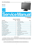
1
HannStarDisplayCorp.
Document Title
HW191A_XY _HSM
Document No.
Page No.
Revision
1 / 72
07/08/13
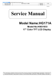
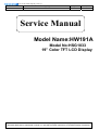
Service Manual
Model Name:HW191A
Model No:HSG1033
19” Color TFT LCD Display
The information contained in this document is the exclusive property of HannStar Display Corporation. It shall not be
disclosed,distributed or reproduced in whole or in part without written permission of HannStar Display Corporation.
HannStarDisplayCorp.
Document Title
HW191A_XY _HSM
Document No.
Page No.
Revision
2 / 72
07/08/13
Copyright
Copyright © 2006 by HannStar Corporation. All rights reserved. No part of this publication
may be reproduced, transmitted, transcribed, stored in a retrieval system, or translated into
any
language or computer language, in any form or by any means, electronic, mechanical,
magnetic, optical, chemical, manual or otherwise, without the prior written permission of
HannStar Corporation.
Disclaimer
HannStar makes no representations or warranties, either expressed or implied, with respect to
the contents hereof and specifically disclaims any warranty of merchantability or fitness for
any particular purpose. Further, HannStar reserves the right to revise this publication and to
make changes from time to time in the contents hereof without obligation of HannStar to notify
any person of such revision or changes.
Trademarks
Opt quest is a registered trademark of HannStar Corporation.
HannStar is a registered trademark of HannStar Corporation.
All other trademarks used within this document are the property of their respective owners.
Revision History
Revision
SM Editing Date
A00
Oct.-17-08
ECR Number
Description of Changes
TPV Model
First Version Release
T98HRDDTWNHZACE
T98HRDDBWNZHACE
A01
Nov.-04-08
Add New Model In Item 16
T98HRDDYWNHZACE
T98HRDDKWNHZACE
The information contained in this document is the exclusive property of HannStar Display Corporation. It shall not be
disclosed,distributed or reproduced in whole or in part without written permission of HannStar Display Corporation.
HannStarDisplayCorp.
Document Title
HW191A_XY _HSM
Document No.
Page No.
Revision
3 / 72
07/08/13
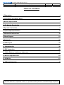
TABLE OF CONTENTS
1. Dimensions
4
2. Precautions and Safety Notice
6
3.Monitor Specification
7
4.LCD Monitor Description
8
5.Operation Instruction
9
6. Input/output Specification
14
7. Mechanical Instructions
18
8. Block Diagram
21
9.Schematic
27
10.PCB Layout
34
11. Maintainability
39
12 DDC Instruction
45
13. White-Balance, Luminance adjustment
58
14.Monitor Exploded View
60
15. BOM List
61
16. Different Parts List
72
The information contained in this document is the exclusive property of HannStar Display Corporation. It shall not be
disclosed,distributed or reproduced in whole or in part without written permission of HannStar Display Corporation.
HannStarDisplayCorp.
Document Title
HW191A_XY _HSM
Document No.
Page No.
Revision
4 / 72
07/08/13
1. Dimensions
1.1 Front View
1.2 Back View
The information contained in this document is the exclusive property of HannStar Display Corporation. It shall not be
disclosed,distributed or reproduced in whole or in part without written permission of HannStar Display Corporation.
HannStarDisplayCorp.
Document Title
HW191A_XY _HSM
Document No.
Page No.
Revision
5 / 72
07/08/13
1.3 Side View
1.4 Bottom View
The information contained in this document is the exclusive property of HannStar Display Corporation. It shall not be
disclosed,distributed or reproduced in whole or in part without written permission of HannStar Display Corporation.
HannStarDisplayCorp.
Document Title
HW191A_XY _HSM
Document No.
Page No.
Revision
6 / 72
07/08/13
2. Precautions and Safety Notices
Proper service and repair is important to the safe, reliable operation of all AOC Company Equipment. The service
procedures recommended by AOC and described in this service manual are effective methods of performing service
operations. Some of these service operations require the use of tools specially designed for the purpose. The special tools
should be used when and as recommended.
It is important to note that this manual contains various CAUTIONS and NOTICES which should be carefully read in order
to minimize the risk of personal injury to service personnel. The possibility exists that improper service methods may
damage the equipment. It is also important to understand that these CAUTIONS and NOTICES ARE NOT EXHAUSTIVE.
AOC could not possibly know, evaluate and advise the service trade of all conceivable ways in which service might be
done or of the possible hazardous consequences of each way. Consequently, AOC has not undertaken any such broad
evaluation. Accordingly, a servicer who uses a service procedure or tool which is not recommended by AOC must first
satisfy himself thoroughly that neither his safety nor the safe operation of the equipment will be jeopardized by the service
method selected.
Hereafter throughout this manual, AOC Company will be referred to as AOC.
WARNING
Use of substitute replacement parts, which do not have the same, specified safety characteristics may create shock, fire, or
other hazards.
Under no circumstances should the original design be modified or altered without written permission from AOC. AOC
assumes no liability, express or implied, arising out of any unauthorized modification of design.
Servicer assumes all liability.
FOR PRODUCTS CONTAINING LASER:
DANGER-Invisible laser radiation when open AVOID DIRECT EXPOSURE TO BEAM.
CAUTION-Use of controls or adjustments or performance of procedures other than those specified herein may result in
hazardous radiation exposure.
CAUTION -The use of optical instruments with this product will increase eye hazard.
TO ENSURE THE CONTINUED RELIABILITY OF THIS PRODUCT, USE ONLY ORIGINAL MANUFACTURER'S
REPLACEMENT PARTS, WHICH ARE LISTED WITH THEIR PART NUMBERS IN THE PARTS LIST SECTION OF THIS
SERVICE MANUAL.
Take care during handling the LCD module with backlight unit.
-Must mount the module using mounting holes arranged in four corners.
-Do not press on the panel, edge of the frame strongly or electric shock as this will result in damage to the screen.
-Do not scratch or press on the panel with any sharp objects, such as pencil or pen as this may result in damage to the
panel.
-Protect the module from the ESD as it may damage the electronic circuit (C-MOS).
-Make certain that treatment person’s body is grounded through wristband.
-Do not leave the module in high temperature and in areas of high humidity for a long time.
-Avoid contact with water as it may a short circuit within the module.
‐If the surface of panel becomes dirty, please wipe it off with a soft material. (Cleaning with a dirty or rough cloth may damage the panel.) The information contained in this document is the exclusive property of HannStar Display Corporation. It shall not be
disclosed,distributed or reproduced in whole or in part without written permission of HannStar Display Corporation.
HannStarDisplayCorp.
Document Title
HW191A_XY _HSM
Document No.
Page No.
Revision
7 / 72
07/08/13
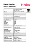
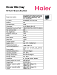
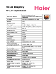
3. Monitor Specifications
The information contained in this document is the exclusive property of HannStar Display Corporation. It shall not be
disclosed,distributed or reproduced in whole or in part without written permission of HannStar Display Corporation.
HannStarDisplayCorp.
Document Title
HW191A_XY _HSM
Document No.
Page No.
Revision
8 / 72
07/08/13
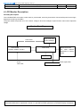
4. LCD Monitor Description
Assembly Description
The LCD MONITOR will contain a main board, a power board, and a key board which house the flat panel control logic,
brightness control logic and DDC.
The power board will provide AC to DC Inverter voltage to drive the backlight of panel and the main board chips each
voltage.
Monitor Block Diagram
CCFL Drive.
Power board
Flat Panel and
CCFL backlight
main board
(Include: adapter, inverter)
RS232 Connector
For
white
balance
adjustment in factory
mode
Key board
AC-IN
100V-240V
HOST Computer
Video signal, DDC
The information contained in this document is the exclusive property of HannStar Display Corporation. It shall not be
disclosed,distributed or reproduced in whole or in part without written permission of HannStar Display Corporation.
HannStarDisplayCorp.
Document Title
HW191A_XY _HSM
Document No.
Page No.
Revision
9 / 72
07/08/13
5. Operating Instructions
5.1 General Instructions
Press the power button to turn the monitor on or off. The control buttons are located in the front of the monitor.
By changing these settings, the picture can be adjusted to your personal preferences.
-
The power cord should be connected.
-
Connect the video cable from the monitor to the video card.
-
Press the power button to turn on the monitor, the power indicator will light up.
5.2 Control Buttons
The information contained in this document is the exclusive property of HannStar Display Corporation. It shall not be
disclosed,distributed or reproduced in whole or in part without written permission of HannStar Display Corporation.
HannStarDisplayCorp.
Document Title
HW191A_XY _HSM
Document No.
Page No.
Revision
10 / 72
07/08/13
FRONT PANEL CONTROL
• Power Button:
Press this button to switch ON/OFF monitor’s power.
• Power Indicator:
Green — Power On mode.
Orange — Power Saving mode.
• MENU / RETURN:
1. Turn the OSD menu on/off or return to the previous menu.
2. Exit OSD menu when in volume OSD status.
• Adjust ▲▼:
1. Adjust Brightness and volume when the OSD is off.
2. Navigate through adjustment icons when OSD is ON or adjust a function when function is
activated.
• A Button:
HW191A:
1. The OSD menu is used as “confirmation” function during start-up.
2. The 「Auto adjustment」 function works only for VGA input. (The auto adjustment function is
used to optimize the 「horizontal position」, 「vertical position」,「clock」,and 「phase」.)
NOTES:
• Do not install the monitor in a location near heat sources such as radiators or air dusts, or in a
place subject to direct sunlight, or excessive dust or mechanical vibration or shock.
• Save the original shipping box and packing materials, as they will come in handy if you ever have
to ship your monitor.
• For maximum protection, repackage your monitor as it was originally packed at the factory.
• To keep the monitor looking new, periodically clean it with a soft cloth. Stubborn stains may be
removed with a cloth lightly dampened with a mild detergent solution. Never use strong solvents
such as thinner, benzene, or abrasive cleaners, since these will damage the cabinet. As a safety
precaution, always unplug the monitor before cleaning it.
The information contained in this document is the exclusive property of HannStar Display Corporation. It shall not be
disclosed,distributed or reproduced in whole or in part without written permission of HannStar Display Corporation.
HannStarDisplayCorp.
Document Title
HW191A_XY _HSM
Document No.
Page No.
Revision
11 / 72
07/08/13
5.3 Adjusting the Picture
The information contained in this document is the exclusive property of HannStar Display Corporation. It shall not be
disclosed,distributed or reproduced in whole or in part without written permission of HannStar Display Corporation.
HannStarDisplayCorp.
Document Title
HW191A_XY _HSM
Document No.
Page No.
Revision
12 / 72
07/08/13
The information contained in this document is the exclusive property of HannStar Display Corporation. It shall not be
disclosed,distributed or reproduced in whole or in part without written permission of HannStar Display Corporation.
HannStarDisplayCorp.
Document Title
HW191A_XY _HSM
Document No.
Page No.
Revision
13 / 72
07/08/13
The information contained in this document is the exclusive property of HannStar Display Corporation. It shall not be
disclosed,distributed or reproduced in whole or in part without written permission of HannStar Display Corporation.
HannStarDisplayCorp.
Document Title
HW191A_XY _HSM
Document No.
Page No.
Revision
14 / 72
07/08/13
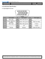
6. Input/output Specification
6.1 Input Signal Connector
The information contained in this document is the exclusive property of HannStar Display Corporation. It shall not be
disclosed,distributed or reproduced in whole or in part without written permission of HannStar Display Corporation.
HannStarDisplayCorp.
Document Title
HW191A_XY _HSM
Document No.
Page No.
Revision
15 / 72
07/08/13
6.2 Factory Preset Display Modes
The information contained in this document is the exclusive property of HannStar Display Corporation. It shall not be
disclosed,distributed or reproduced in whole or in part without written permission of HannStar Display Corporation.
HannStarDisplayCorp.
Document Title
HW191A_XY _HSM
Document No.
Page No.
Revision
16 / 72
07/08/13
6.3 Panel Specification
HannStar Display model HSD190MGW1-A02 is a color active matrix thin film transistor (TFT) liquid crystal display (LCD)
that uses amorphous silicon TFT as switching device. This model is composed of a TFT LCD panel, the voltage reference,
common voltage, DC-DC converter, column, and row driver circuit. This TFT LCD has a 19-inch diagonally measured
active display area with WXGA+ resolution (900 vertical by 1440 horizontal pixel array).
6.3.1 Features
_ 19” WXGA+ TN(Twisted Nematic) mode TFT LCD panel
_ High speed response time
_ 4 CCFLs Backlight system
_ Supported WXGA+ (V:900 lines, H:1440 pixels) resolution
_ Supported to 75Hz refresh rate
_ LCD Timing Controller
_ RoHS compliance
6.3.2 Display Characteristics
6.3.3 Electrical Characteristics
1. TFT LCD Module
2. Backlight Unit
The information contained in this document is the exclusive property of HannStar Display Corporation. It shall not be
disclosed,distributed or reproduced in whole or in part without written permission of HannStar Display Corporation.
HannStarDisplayCorp.
Document Title
HW191A_XY _HSM
Document No.
Page No.
Revision
17 / 72
07/08/13
6.3.4 Optical Characteristics
Measuring Condition
_ Measuring surrounding: dark room
_ Lamp current IBL: (6.5)±0.1mA, lamp freq. FL= 50KHz, Inverter: TDK TBD332LR
_ VDD1=5.0V, fV=60Hz, fDCLK=53.25MHz
_ Surrounding temperature : 25±2oC
_ 30min. Warm-up time.
The information contained in this document is the exclusive property of HannStar Display Corporation. It shall not be
disclosed,distributed or reproduced in whole or in part without written permission of HannStar Display Corporation.
HannStarDisplayCorp.
Document Title
HW191A_XY _HSM
Document No.
Page No.
Revision
18 / 72
07/08/13
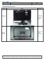
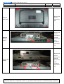
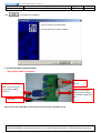
7. Mechanical Instructions
Step
Preparatio
n
Figure
Description
Lay the LCD
on a flat, soft
and clean
surface.
Remove the
Remove
screws
the base
remarked in
red
The information contained in this document is the exclusive property of HannStar Display Corporation. It shall not be
disclosed,distributed or reproduced in whole or in part without written permission of HannStar Display Corporation.
HannStarDisplayCorp.
Document Title
HW191A_XY _HSM
Document No.
Page No.
Revision
19 / 72
07/08/13
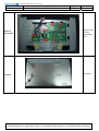
Remove the
Remove
screws
rear cover
remarked in
red
Remove the
screws
remarked in
Remove
red and
the key
disconnecte
board
d the
connecter
remarked in
red
Remove the
screws
remarked in
remove the
shield
red and
disconnecte
d the
connecter
remarked in
red
The information contained in this document is the exclusive property of HannStar Display Corporation. It shall not be
disclosed,distributed or reproduced in whole or in part without written permission of HannStar Display Corporation.
HannStarDisplayCorp.
Document Title
HW191A_XY _HSM
Document No.
Page No.
Revision
20 / 72
07/08/13
Remove
the boards
Remove the
screws
remarked in
red
The end
The panel
The information contained in this document is the exclusive property of HannStar Display Corporation. It shall not be
disclosed,distributed or reproduced in whole or in part without written permission of HannStar Display Corporation.
HannStarDisplayCorp.
Document Title
HW191A_XY _HSM
Document No.
Page No.
Revision
21 / 72
07/08/13
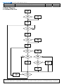
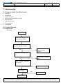
8. Block Diagram
8.1 Software Flow Chat
1
Y
2
3
N
4
N
5
Y
6
N
7
8
Y
9
10
N
11
Y
N 12
Y
14
13
N
Y
15
N
16 Y
17
18 N 19
Y
The information contained in this document is the exclusive property of HannStar Display Corporation. It shall not be
disclosed,distributed or reproduced in whole or in part without written permission of HannStar Display Corporation.
HannStarDisplayCorp.
Document Title
HW191A_XY _HSM
Document No.
1) MCU initialize.
Page No.
Revision
22 / 72
07/08/13
2) Is the EPROM blank?
3) Program the EPROM by default values.
4) Get the PWM value of brightness from EPROM.
5) Is the power key pressed?
6) Clear all global flags.
7) Are the AUTO and SELECT keys pressed?
8) Enter factory mode.
9) Save the power key status into EPROM.
Turn on the LED and set it to green color.
Scalar initializes.
10) In standby mode?
11) Update the lifetime of back light.
12) Check the analog port, are there any signals coming?
13) Does the scalar send out an interrupt request?
14) Wake up the scalar.
15) Are there any signals coming from analog port?
16) Display "No connection Check Signal Cable" message. And go into standby mode after the message
disappear.
17) Program the scalar to be able to show the coming mode.
18) Process the OSD display.
19) Read the keyboard. Is the power key pressed?
The information contained in this document is the exclusive property of HannStar Display Corporation. It shall not be
disclosed,distributed or reproduced in whole or in part without written permission of HannStar Display Corporation.
HannStarDisplayCorp.
Document Title
HW191A_XY _HSM
Document No.
Page No.
Revision
23 / 72
07/08/13
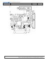
8.2 Electrical Block Diagram
8.2.1 Main Board
Crystal
24MHZ
Panel Interface
(X401)
(CN101)
MCU
Scalar IC RTD2025L
RTD2120L
(Include ADC, OSD)
(U401)
(U501)
H sync
V sync
RGB EEPROM
OSD
Control Interface
(KEYPAD)
M24C16
D-Sub
(U403)
Connector
(CN301)
EEPROM
AS431AN-A
(U402) The information contained in this document is the exclusive property of HannStar Display Corporation. It shall not be
disclosed,distributed or reproduced in whole or in part without written permission of HannStar Display Corporation.
HannStarDisplayCorp.
Document Title
HW191A_XY _HSM
Document No.
Page No.
Revision
24 / 72
07/08/13
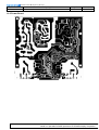
8.2.2 Power/Inverter Board
AC input
Bridge
Rectifier
and Filter
EMI filter
Transformer
Rectifier
diodes
Start Circuit: R904,R932,R933
CN902
5V
Feedback
Circuit
PWM
Control IC
12V
ON/OFF
Output
Circuit
Lamp
Feedback
Circuit
Transformer
Over
Voltage
MOSFET
PWM
Control IC
ON/OFF
Control
DIM
DIM
The information contained in this document is the exclusive property of HannStar Display Corporation. It shall not be
disclosed,distributed or reproduced in whole or in part without written permission of HannStar Display Corporation.
HannStarDisplayCorp.
Document Title
HW191A_XY _HSM
Document No.
Page No.
Revision
25 / 72
07/08/13
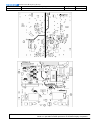
8.3 Mechanical Block Diagram
8.3.1 Assembly Block Main Board*1
Screw*1
Bezel*1
Len *1
Assy,base*2
Screw*6
Speaker*2
Screw*4
Main Frame
Power Board
HW191A,Panel *1
Screw*3
Bezel*1
Key Board *1
Button*1
Keypad cable*1
Back Cover*1
Assy,Stand*1
Hinge*1
Rubber Foot*6
Assy stand*1
HW191A
LCD Monitor
The information contained in this document is the exclusive property of HannStar Display Corporation. It shall not be
disclosed,distributed or reproduced in whole or in part without written permission of HannStar Display Corporation.
HannStarDisplayCorp.
Document Title
HW191A_XY _HSM
Document No.
Page No.
Revision
26 / 72
07/08/13
8.3.1 Disassembly Block HW191A
LCD Monitor
Assy Base*1
Rubber foot
Base*1
Assy Stand*1
Stand*1
Hinge*1
Back Cover*1
Bezel*1
Len *1
Bezel*1
Button*1
Key Board *1
Keypad cable*1
Screw*2
Main Board*1
Main Frame
Power Board
Screw*1
HW191A,Panel *1
Screw*3
Speaker*2
Screw*4
The information contained in this document is the exclusive property of HannStar Display Corporation. It shall not be
disclosed,distributed or reproduced in whole or in part without written permission of HannStar Display Corporation.
HannStarDisplayCorp.
Document Title
Document No.
HW191A_XY _HSM
Page No.
Revision
27 27 / 72 07/08/03
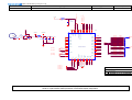
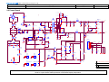
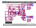
9. Schematic
9.1 Main Board
CN201
1
2
3
4
5
6
7
8
9
CMVCC
CMVCC
CMVCC
BKLT-VBRI
BKLT-EN
C_PANEL_INDEX
Volume#
Mute
MVCC
DIM#
{4}
PANEL_ID#
Volume#
Mute
{4}
{4}
{4}
FB202
NC
CMVCC
FB201
3
Panel ID(3.3V PWM)
2
+
AP1117E33LA
C204
C205
C203
100uF/25V
+
1
C202
100uF/25V
VOUT
VSS
120 VIN
CONN
'07-01-10 change to Elite
VCC3
U201
0.1uF/16V
'07-01-10 change to Elite
0.1uF/16V
Back light
Dimming(3.3V PWM)
VCC3
* BKLT-EN High ON(3.3V)
BKLT-EN
R202
4K7 1/16W
R201
200 1/16W
C206
0.1uF/16V
Q202
PMBS3904
INV_ON#
{4}
VCC3
R207
120R 1/16W
'06-11-3 Remove R209(470 ohm)
CN202
1
2
3
4
5
6
KEY 0
KEY 1
POWER_KEY #
LED_G
LED_R
Q204
PMBS3906
R210
KEY 0
{4}
KEY 1
{4}
POWER_KEY # {4}
LED_R
C209
ZD203
NC
0.1uF/16V
2
C201
ZD201
NC
LED_G
'06-12-29-3 Change R207,R208 Value
from 470ohm to 120ohm
10K 1/16W
R213
10K 1/16W
LED_G#
{4}
{4}
C210
0.1uF/16V
0.1uF/16V
TPV(Top Victory)Electronics Co.,Ltd
Title
Power
Near to Connect
LED_R#
Q205
PMBS3906
1
1
NC
1
ZD202
2
'06-12-29-3 Remove R211,R212(470ohm)
2
CONN
R208
120R 1/16W
Size
A
Document Number
Date:
Sunday , January 06, 2008
Rev
1.0
G2498-1-2-X-1-080104
Sheet
2
of
6
The information contained in this document is the exclusive property of HanStar Display Corporation. It shall not be disclosed,distributed or reproduced in
whole or in part without written permission of HannStar Display Corporation.
HannStarDisplayCorp.
Document Title
Document No.
HW191A_XY _HSM
Page No.
Revision
28 28 / 72 07/08/03
DSUB_V
{4}
{5}
{5}
C302 C303
FB302
22pF
VGA_B+
13
DDC1_SDA
12
11
17
ZD307
UDZS5.6B
VGA_CON
DSUB_5V
VGA_BVGA_B+
VGA_GVGA_G+
VGA_RVGA_R+
DSUB_5V
2
DSUB_H
10
5
9
4
8
3
7
2
6
1
ZD305
R307
75R 1/16W
C305
5pF/50V
UDZS5.6B
ZD304
UDZS5.6B
RTD_B+
RTD_B+
{5}
RTD_B-
{5}
RTD_G+
{5}
RTD_G-
{5}
RTD_R+
{5}
RTD_R-
{5}
0.047uF
R308 100R 1/16W C306
VGA_B-
RTD_B-
0.047uF
FB301
1
14
2
15
R306 100R 1/16W C304
2
R311 100R 1/16W
DSUB_CONNECT {4}
1
DDC1_SCL
DSUB_V
BEAD
VGA_G+
1
DB15
BEAD
R309 100R 1/16W C307
2
R310
75R 1/16W
1
ZD301
UDZS5.6B
1
1
22pF
16
DDC1_SDA
1
RTD_H
RTD_V
CN301
DDC1_SCL
2
{4}
R305
2.2K 1/16W
2.2K 1/16W
2
{4}
R304
ZD303
UDZS5.6B
1
ZD302
UDZS5.6B
12/29 change
ZD302 ZD303
from NC to
insert
R301 100R 1/16W
R303 100R 1/16W
2
2
R302 0R05 1/16W
C308
5pF/50V
RTD_G+
0.047uF
R312 100R 1/16W C309
VGA_G-
RTD_G-
0.047uF
FB303
VGA_R+
1
BEAD
R313 100R 1/16W C301
2
R314
75R 1/16W
C310
5pF/50V
3 VGA_B+
3
VGA_G+
VGA_R+
3
D302
BAV99
0.047uF
R315 100R 1/16W C311
VGA_R-
D301
BAV99
RTD_R+
RTD_R-
0.047uF
D303
BAV99
1
2
1
2
1
2
CMVCC
C315
0.1uF/16V
TPV(Top Victory)Electronics Co.,Ltd
Title
Input
Size
A
Document Number
Date:
Sunday , January 06, 2008
G2498-1-2-X-1-080104
Sheet
3
of
Rev
1.0
6
The information contained in this document is the exclusive property of HanStar Display Corporation. It shall not be disclosed,distributed or reproduced in
whole or in part without written permission of HannStar Display Corporation.
HannStarDisplayCorp.
Document Title
Document No.
HW191A_XY _HSM
Page No.
Revision
29 29 / 72 07/08/03
DSUB_5V CMVCC
'06-11-24 D402 change
Value from BAT54 to
BAV70
C402
D402
BAV70
1uF 10V
Q401
PMBS3904
MCU_VCC_S
CMVCC
D401
BAT54C(NC)
2
1
Reserve for powerBoard
CMVCC=3V
3
MCU_VCC
MCU_VCC
C404
R402
1K 1/16W
C412
R405 R406 R407
R404
10K 1/16W
1
1
2
3
4
2
BAT54C
NC VCC
NC WC
NC SCL
VSS SDA
8
7
6
5
NC/4K7 1/16W
U403
3
U402
AZ431AN-AE1
NC/4K7 1/16W
NC/4K7 1/16W
NC/0.22uF
R403
1uF 10V
3.9K 1/16W
R408
R409
R410
NC/100R 1/16W
NC/100R 1/16W
NC/100R 1/16W
WP
IICSCL
IICSDA
NC/M24C16
MCU_VCC
2006-11/23 change R413-4, pull high pin
from DSUB_VCC ,DVI_VCC to MCU_VCC
MCU_VCC
PANEL_VCC
R416
10K 1/16W
Closed to X'tal
C401
10pF
2
R439
NC
C411
10pF
41
40
39
38
37
36
35
34
33
P1.0/T2
P1.1
P1.2
P1.3
P1.4
P1.5
P1.6
P1.7
28
27
26
25
24
23
22
21
20
R425
10K 1/16W
DSUB_V1
R427
0R05 1/16W DSUB_V
R429
0R05 1/16W CRY STAR_OUT
DSUB_CONNECT
R433 100R 1/16W
R434 100R 1/16W
R435 100R 1/16W
POWER_KEY#
KEY 1
KEY 0
DSUB_V
{3}
CRYSTAR_OUT {5}
DSUB_CONNECT {3}
POWER_KEY # {2}
KEY1
{2}
KEY0
{2}
MVCC
R431
6K8 1/16W
2006-11-3 change R431 from 1K to 6.8K
RTD2120L-LF
24mhz
X401
C403
0.1uF/16V
1
2007-01-11 ADD
VCC
4
R415
6K8 1/16W
RTD2120L
P6.7
P6.6/CLKO1
P6.5
P6.4
P6.3/ADC3
P6.2/ADC2
P6.1/ADC1
P6.0/ADC0
32
31
30
29
NC
NC
LED_G#
LED_R#
XO
XI
LED_G#
LED_R#
P3.2/INT0
P3.3/INT1
P3.4/T0
P3.5/T1
P7.6/CLKO2
P7.7
15
16
{2}
{2}
9
10
11
12
13
14
MCU_VCC
VSYNC
42
43
2006-11/7 change R426,R428 from
100 ohm to 22 ohm
ASCL1/P3.0/RXD
ASDA1/P3.1/TXD
RTD_SD3/SDI {5}
RTD_SCLK
{5}
C409
NC(22pF/16V)
NC
NC
NC
NC
NC
NC
5
8
P5.0/PWM0
P5.1/PWM1
P5.2/PWM2
P5.3/PWM3
P5.4/PWM4
P5.5/PWM5
DSCL2/P5.6
DSDA2/P5.7
NC
NC
22R 1/16W
22R 1/16W
U401
R412
4K7 1/16W
IICSDA
IICSCL
WP
RTD_SD3/SDI
RTD_SCLK
18
19
R426
R428
from
44
45
46
47
48
1
2
3
RST
2K 1/16W
2007-1-15 change R413, R414
4.7K to 2.2K
0.1uF/16V
R411
4K7 1/16W
6
7
DDC1_SCL
DDC1_SDA
R414
C406
10uF/50V
VSS
DDC1_SCL
DDC1_SDA
R451 R413
C405
+
17
{3}
{3}
1K 1/16W
Volume#
Mute
PANEL_ID#
DIM#
PPWR_ON#
INV_ON#
1K 1/16W
{2}
{2}
{2}
{2}
{6}
{2}
2006-11/7 R423-R424
change from 100R to
1K
Volume#
R420
NC
Mute
R422
NC
PANEL_ID#
R423
1K 1/16W
DIM#
R424
1K 1/16W
PPWR_ON#
R430
100R 1/16W
INV_ON#
R432
100R 1/16W
R454 R453
4K7 1/16W
2006-11/7 Add pull high R451 to MVCC
,R453,R454 pull up MCU_VCC
MCU_VCC_S
2K 1/16W
VCC3
R437
3.9K 1/16W
2007-1/3 change ref from Y401
to X401
MCU_VCC
R401
3.9K 1/16W
R438
10K 1/16W
R436
10K 1/16W
C410
0.1uF/16V
2006-12-8 change R437,R401 from 10K to 3.9K
2007-1/18 change X401 to 75
Degree
Closed to MCU
TPV(Top Victory)Electronics Co.,Ltd
Title
MCU/RTD2120
Size
A
Document Number
Date:
Friday , January 25, 2008
G2498-1-2-X-1-080104
Sheet
4
of
Rev
1.0
6
The information contained in this document is the exclusive property of HanStar Display Corporation. It shall not be disclosed,distributed or reproduced in
whole or in part without written permission of HannStar Display Corporation.
HannStarDisplayCorp.
Document Title
Document No.
HW191A_XY _HSM
Page No.
Revision
30 30 / 72 12
{3}
{3}
{3}
{3}
RTD_GRTD_G+
RTD_RRTD_R+
TXO0+
RXO0-
RXO0+
37
DGND
39
38
TXO0-
VCCK
PGND
R1.8DVCC
40
{4}
RTD_SD3/SDI
RTD_SCLK
RTD_SCLK
RTD_SD3/SDI
41
43
42
SCL
SDA
CRYSTAR_OUT
CRYSTAR_OUT
44
TXE0-
ADC_GND
TXE0+
B-
TXE1-
B+
TXE1+
13
14
15
16
17
18
19
20
RTD_G-
RTD_G+
RTD_R-
RTD_R+
R1.8DVCC
BJT_B
R1.8DVCC
DGND
36
RXO1-
35
RXO1+
34
RXO2-
33
RXO2+
32
RXOC-
31
RXOC+
30
RXO3-
29
RXO3+
28
RXE0-
27
RXE0+
26
RXE1-
25
RXE1+
RXOCRXOC+
LVDS_O0
LVDS_O1
LVDS_O2
LVDS_O3
LVDS_O4
LVDS_O5
RXO0RXO0+
RXO1RXO1+
RXO2RXO2+
LVDS_O6
LVDS_O7
LVDS_O8
LVDS_O9
RXOCRXOC+
RXO3RXO3+
LVDS_E0
LVDS_E1
LVDS_E2
LVDS_E3
RXE0RXE0+
RXE1RXE1+
LVDS_E4
LVDS_E5
LVDS_E6
LVDS_E7
LVDS_E8
LVDS_E9
RXE2RXE2+
RXECRXEC+
RXE3RXE3+
LVDS_O[0..9]
{6}
LVDS_E[0..9]
{6}
TXE2-
11
AHS
24
RTD_BRTD_B+
TXO3+
G-
{3} RTD_B+
TXO3-
RTD2025L QFN-48
AVS
RXE2-
{3} RTD_B-
9
10
V7/RXCN
TXE2+
DGND
TXOC+
23
RTD_H
{3} RTD_H
8
V6/RXCP
RXE2+
RTD_V
{3} RTD_V
TXOC-
TXE3-
7
TXO2+
V5/RX0N
TXE3+
6
V4/RX0P
22
5
TXO2-
RXE3-
DGND
V3/RX1N
21
4
TXO1+
RXE3+
3
V2/RX1P
U501
TXO1-
PGND
0.1uF/16V
0.1uF/16V
0.1uF/16V
V1/REXT
DDCSDA/PWM1/IRQ
2
VCCK
C501
DDCSCL/PWM0
C507
BJT_B
22uF/50V
C506
ADC_VDD
C505 +
TMDS_VDD
1
FB503
120 46
TMDS_VDD
MMBT2907AK
47
48
V0/RX2N
Q502
R+
3.3 2W
R-
R507
R1.8DVCC
G+
VCC3
VCLK/RX2P
BJT_B
1.8AVCC
Q501
MMBT2907AK
45
C503
0.1uF/16V
XIN
VCC3
FB502
120 {4}
{4}
07/08/03
TPV(Top Victory)Electronics Co.,Ltd
R1.8DVCC
Title
RTD2025L
Size
A
Document Number
Date:
Sunday , January 06, 2008
G2498-1-2-X-1-080104
Sheet
The information contained in this document is the exclusive property of HanStar Display Corporation. It shall not be disclosed,distributed or reproduced in
whole or in part without written permission of HannStar Display Corporation.
5
of
Rev
1.0
6
HannStarDisplayCorp.
Document Title
Document No.
HW191A_XY _HSM
Page No.
Revision
31 31 / 72 07/08/03
LVDS Panel ( Normal Type )
{5}
CN601
LVDS_O[0..9]
{5}
LVDS_E[0..9]
LVDS_O0
LVDS_O1
LVDS_O2
LVDS_O3
LVDS_O4
LVDS_O5
RXO0RXO0+
RXO1RXO1+
RXO2RXO2+
LVDS_O6
LVDS_O7
LVDS_O8
LVDS_O9
RXOCRXOC+
RXO3RXO3+
LVDS_E0
LVDS_E1
LVDS_E2
LVDS_E3
RXE0RXE0+
RXE1RXE1+
LVDS_E4
LVDS_E5
LVDS_E6
LVDS_E7
LVDS_E8
LVDS_E9
RXE2RXE2+
RXECRXEC+
RXE3RXE3+
RXO0RXO1RXO2RXOCRXO3RXE0RXE1RXE2RXECRXE3-
1
3
5
7
9
11
13
15
17
19
21
23
2
4
6
8
10
12
14
16
18
20
22
24
CONN
RXO0+
RXO1+
RXO2+
RXOC+
RXO3+
RXE0+
RXE1+
RXE2+
RXEC+
RXE3+
PANEL_VCC
R602
330R 1/8W
R606
NC(R0805)
C602
0.01uF/25V
'07-01-04 Add R606(NC)
3D
CMVCC
1
G
R605
4K7 1/16W
R601
R604
2006-11-7 Add pull up 4K7 to MVCC
{4}
PPWR_ON#
PPWR_ON#
AO3401L
C603
10K 1/16W
Q602
47K 1/16W
PMBS3906
2
S
0.1uF/16V
Q601
AO3401
PANEL_VCC
PANEL_VCC
FB601
120 C604
47uF/25V
+
TPV(Top Victory)Electronics Co.,Ltd
Title
Output
Size
A
Document Number
Date:
Sunday , January 06, 2008
G2498-1-2-X-1-080104
Sheet
6
of
Rev
1.0
6
TPV(Top Victory)Electronics Co.,Ltd
Realtek Semiconductor Corp.
A
G2498-1-2-X-1-080104
The information contained in this document is the exclusive property of HanStar Display Corporation. It shall not be disclosed,distributed or reproduced in
whole or in part without written permission of HannStar Display Corporation.
HannStarDisplayCorp.
Document Title
Document No.
HW191A_XY _HSM
Page No.
Revision
32 32 / 72 07/08/03
1
9.2 Power Board
2
R905
10K 1/4W
C901
1000pF
C912
0.1uF
+
C916
0.1uF
1
ZD901
NC
IC901
4.0mH
RT
HV
COMPNC
CS VCC
GNDOUT
8
7
6
5
D910 LL4148WP
3
12
!
Q900
STP10NK70ZFP
R954
47 1/4W
R955
47 1/4W
R956
47 1/4W
R916
0.43 2W
3
1
2
1
2
R925
1K 1/8W
IC902
PC123X2Y FZOF
GND1
GND
F901
FUSE
GND2
GND
+ C926
1000uF16V
+
C927
470uF/16V
CHANGE 13X20mm
1
2
3
4
5
6
7
8
9
10
C928
0.1uF
!
C900
2200PF
FB902
1
1
2
HS5
HEAT SINK(D920)
1
2
Q910
NC
C915
NC
ZD921
RLZ13B
ZD922
RLZ5.1B
D915
D916
LL4148WP
LL4148WP
R924
3K6 1/8W
R923
10K 1/8W
D911
NC
1
2
HS1
HEAT SINK(Q900)
1
1
NC
JUMPER
1
!
NR901
NTCR
CN901
SOCKET
+5V
C921
0.001uF/500V
R922
470R 1/8W
3
2
F903
2
R913
1K 1/8W
R928
1K 1/8W
2
JUMPER
!
L922
3.5uH
D922
31DQ06FC3
R903
1K 1/8W
0.001uF
CN902
CONNECTOR
C914
470pF/25V
!
C924
1
8
IC903
KIA431A-AT/P
ON/OFF
DIM
12V
+5V
1
C913
220pF
R902
330K 1/4W
RLZ13B
R908
470 1/8W
Q902
PMBS3904
2
!
!
150 1W
R931
10K 1/4W
2
2
!
+
ZD920
C904
6
1
4
R900
330K 1/4W
+
D921
NC
1
330K 1/4W
R901
+
ZD902
NC
C909 0.47uF
10
R910
2.2 1/4W
R912
10R 1/4W
R915
10K 1/8W
LD7575PS
11
FB901
BEAD
1
1
2
3
4
R911
100K 1/8W
!
C911
22uF/50V
2
3 L901 2
+
7
6
4
D901
UF4003PT
!
!
1
D900
BA159GPT
2
VAR901
NC
5
C925
470uF/25V
C903
1000PF
R909
100K 2W
+12V
R907
3
C910
1500PF/2KV
!
F902
0R05 1/4W
2
1
C907
100uF/450V
L921
3.5uH
2
!
!
D920
SBT150-10LST
C923
680uF/25V
4
3
C920
0.001uF/500V
C922
680uF/25V
2
+
C902
1000pF
!
R953
!
L
!
47 1/4W
T901
80GL17T-33-N2
4
9
1 L902 2
4
R952
FB903
BEAD
KBP208G
4
47 1/4W
3
3
R951
1
BD901
+
!
47 1/4W
C931
0.1uF
C930
0.1uF
R926
33K 1/8W
C929
R927
1K 1/8W
0.1uF
R930
1K 1/8W
R929
2.4K 1/8W
AOC (Top Victory) Electronics Co., Ltd
Title
PWPC742GR1
Size
Document Number
Custom
G2594-G-X-X-2-070515
Date:
Thursday , May 17, 2007
The information contained in this document is the exclusive property of HanStar Display Corporation. It shall not be disclosed,distributed or reproduced in
whole or in part without written permission of HannStar Display Corporation.
Sheet
1
of
HannStarDisplayCorp.
Document Title
Document No.
HW191A_XY _HSM
Page No.
Revision
33 33 / 72 07/08/03
PT801
7
POWER X'FMR
6
+12V
R801 0R05 1/10W 5%
1
2
3
4
C801
10pF/3KV
R802
100R 1/8W
L801
NC
1
2
CN802
CONN
1
2
CN803
CONN
R807
1K 1/10W 1%
OLP1
OLP2
D802
BAV99
R811
1K 1/10W 1%
C805
470uF/25V
1
R812
1K 1/10W 1%
2
1
2
5
6
D
7
G
1
Q804
AM9945N-T1-PF
4
R803
2.4K 1/10W
C819
R816 NC
68K 1% 1/10W
D
C804
0.1uF/16V
S
8
Q812
RK7002
D
R815
47K 1/10W
3
CN801
CONN
ZD801
10K 1/8W
FB
D
R817
NC
R806
1K 1/10W 1%
D801
BAV99
G
Q803
PMBS3904
!
1500PF/50V
3
R814
68K 1/10W
4
R804 0R05 1/10W 5%
C803
S
D803
LL4148WP
8
3
DTC
2
C802
1uF/16V
R813
100 1/10W
DIM
C821
1500PF/50V
D813
LL4148WP
1
15 1/4W
15 1/4W
2
R809
NC
R810
4.7K 1/10W
Q801
PDTA144WK
1
ON/OFF
Q802
PDTC144WK
2
3
R850
R805
R808
10K 1/10W
1
FB
+
C823
R818
NC
C806
1uF/16V
R819
10K 1/10W
R853
10K 1/10W
DTC
0.1uF/25V
Q810
PMBS3904
R820
560K 1/10W
Q811
PMBS3904
IC801
180K 1% 1/8W
1
2
3
4
5
6
7
8
1IN+
2IN+
1IN2INFEEDBACK
REF
DTC OUTPUT CTRL
CT
VCC
RT
C2
GND
E2
C1
E1
TL494IDR
R826
NC
R842
47K 1/10W
R843
R825 51K 1% 1/8W
16
15
14
13
12
11
10
9
R844
22R 1/10W 5%
R845
22R 1/10W 5%
Q806
PMBS3906
R847
22R 1/10W 5%
R846
22R 1/10W 5%
C810
0.1uF/25V
R852
10K 1/10W
R848
1K 1/10W 1%
R849
1K 1/10W 1%
!
R829
68K 1% 1/10W
Q807
PMBS3904
B
3
OLP3
1
C812
10pF/3KV
R840
10K 1/10W
OLP4
C824
+ C811
C817
0.0022uF
1
8
R834
1K 1/10W 1%
D809
BAV99
Date:
L802
NC
CN804
CONN
OLP4
R839
1K 1/10W 1%
1
1
2
R835
1K 1/10W 1%
D810
BAV99
C822
2
Size
A3
3
OLP3
15 1/4W
CHANGE UPDATE
TPV(Top victory) Electronics Co.,ltd.
4
R832 0R05 1/10W 5%
1500PF/50V
Title
2
470uF/25V
0.1uF/25V
2
C818
0.0022uF
1
4
G
D
3
S
2
1
3
4
R851
C
E
Q809
AM9945N-T1-PF
D
C813
0.0022uF
R838
10K 1/10W
R830 0R05 1/10W 5%
3
0.1uF/16V
PT802
7
POWER X'FMR
5
C814
D808
BAW56
6
C815
0.0022uF
R836
1M 1/10W 5%
OLP2
S
E
2
G
R833
10K 1/10W
C
D
B
3
R837
15 1/4W
D
Q808
RK7002
1
6
OLP1
7
D807
LL4148WP
R831
10K 1/10W
C816
1500PF/50V
C820
NC
8
D806
BAW56
2
C809
220pF
10K 1/10W
R824
R822 47K 1/10W
C807
0.1uF/16V
3
R828
47K 1/10W
R823
R821
C808
2.2uF/16V
10KOHM 1/10W
1M 1/10W 5%
D812
LL4148WP
R827
1K 1/10W 1%
Q805
PMBS3906
R841
1K 1/10W 1%
1
D811
LL4148WP
FB
00. Engineer Marks,Contents
Document Number
Rev
G
G2594-G-X-X-2-070515
Thursday , May 17, 2007
Sheet
1
of
1
The information contained in this document is the exclusive property of HanStar Display Corporation. It shall not be disclosed,distributed or reproduced in
whole or in part without written permission of HannStar Display Corporation.
HannStarDisplayCorp.
Document Title
HW191A _XY _HSM
Document No.
Page No.
Revision
34 34 / 72
07/08/03
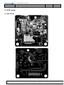
10. PCB Layout
10.1 Main Board
The information contained in this document is the exclusive property of HanStar Display Corporation. It shall not be dis
whole or in part without written permission of HannStar Display Corporation.
HannStarDisplayCorp.
Document Title
HW191A _XY _HSM
Document No.
Page No.
Revision
35 35 / 72
07/08/03
The information contained in this document is the exclusive property of HanStar Display Corporation. It shall not be dis
whole or in part without written permission of HannStar Display Corporation.
HannStarDisplayCorp.
Document Title
HW191A _XY _HSM
Document No.
Page No.
Revision
36 36 / 72
07/08/03
10.2 Power Board
The information contained in this document is the exclusive property of HanStar Display Corporation. It shall not be dis
whole or in part without written permission of HannStar Display Corporation.
HannStarDisplayCorp.
Document Title
HW191A _XY _HSM
Document No.
Page No.
Revision
37 37 / 72
07/08/03
The information contained in this document is the exclusive property of HanStar Display Corporation. It shall not be dis
whole or in part without written permission of HannStar Display Corporation.
HannStarDisplayCorp.
Document Title
HW191A _XY _HSM
Document No.
Page No.
Revision
38 38 / 72
07/08/03
10.3 key board
10.4 Audio board
The information contained in this document is the exclusive property of HanStar Display Corporation. It shall not be dis
whole or in part without written permission of HannStar Display Corporation.
HannStarDisplayCorp.
Document Title
HW191A _XY _HSM
Document No.
Page No.
Revision
39 39 / 72
07/08/03
11. Maintainability
11.1 Equipments and Tools Requirement
1.
Voltmeter.
2.
Oscilloscope.
3.
Pattern Generator.
4.
DDC Tool with Compatible Computer.
5.
Alignment Tool.
6.
LCD Color Analyzer.
7.
Service Manual.
8.
User Manual.
11.2 Trouble Shooting
11.2.1 Main Board
No power
No power
Press power key and look
if the picture is normal NG
Please reinsert and make sure
the AC of 100-240 is normal
NG
OK
Reinsert or check the
Adapter/Inverter
section
Measure U201 PIN2=1.8V ;
NG
Check CN201 or replace
U201, NG
Replace X401 OK
X401
oscillate
waveforms
are normal
OK
Check U501
OK
NG
Replace U501
Replace U401
The information contained in this document is the exclusive property of HannStar Display Corporation. It shall not be
disclosed,distributed or reproduced in whole or in part without written permission of HannStar Display Corporation.
HannStarDisplayCorp.
Document Title
HW191A _XY _HSM
Document No.
Page No.
Revision
40 40 / 72
07/08/03
No picture (LED orange)
No picture
NG
The button if under
X401
control
oscillate
NG
Replace X401
waveform is normal
OK
OK
Check reset circuit of
U501/U401 is normal
NG
Check Correspondent
component Measure U201 PIN2=1.8V ;
OK
ReplaceU501
OK
X401
U401
NG
oscillate
waveform is normal
Replace U201
OK
NG
Replace X401
Check HS/VS from
CN401 is normal OK
NG
Check Correspondent
component Check U501 OK
NG
Replace U501 Replace U401 The information contained in this document is the exclusive property of HannStar Display Corporation. It shall not be
disclosed,distributed or reproduced in whole or in part without written permission of HannStar Display Corporation.
HannStarDisplayCorp.
Document Title
HW191A _XY _HSM
Document No.
Page No.
Revision
41 41 / 72
07/08/03
White screen
White screen
NG
Measure R604 base
is low level?
OK
OK
Check
Q601,
Q602
broken or CN601 solder?
Check Correspondent
component.
X401
oscillate
waveform is normal is
NG
Replace X401
Check reset circuit of
U401 is normal
NG
NG
Check U501
OK
OK
OK
Replace U401
Replace U501
Replace PANEL
The information contained in this document is the exclusive property of HannStar Display Corporation. It shall not be
disclosed,distributed or reproduced in whole or in part without written permission of HannStar Display Corporation.
HannStarDisplayCorp.
Document Title
HW191A _XY _HSM
Document No.
Page No.
Revision
42 42 / 72
07/08/03
11.2.2 Power Board
1) No power
Check CN902 pin3/4 = 5V
NG
Check AC line volt 110V or 220V
OK
NG
Check AC input
Check the voltage of C907 (+)
NG
OK
Check bridge rectified circuit and F901 circuit
Check start voltage for the pin3 of IC901
NG
OK
Check R903, R912, R915 and Change IC901
Check the auxiliary voltage is bigger than
10V and smaller than 20V
NG
OK
1) Check IC901
2) Check IC901 over current protect circuit
Check IC901 pin8 PWM wave
NG
Check IC901,D920,R910,Q902
OK
Check Q900, D901, D910, ZD901, ZD902, IC903 and T901
The information contained in this document is the exclusive property of HannStar Display Corporation. It shall not be
disclosed,distributed or reproduced in whole or in part without written permission of HannStar Display Corporation.
HannStarDisplayCorp.
Document Title
HW191A _XY _HSM
Document No.
Page No.
Revision
43 43 / 72
07/08/03
2.) No Backlight
Check L801= 12V
NG
Check adapter or MB
OK
Check ON/OFF signal
NG
OK
Check Interface board
Check IC801 pin12=5V
NG
Change ON/OFF
OK
Check IC801 PIN9/10 have the output of square wave at short
NG
Check IC801
OK
Check Q804 (D) wave
NG
Check Q801, Q805,Q811,Q806
OK
Check the output of PT801
NG
OK
Check PT801
Check connecter & lamp
The information contained in this document is the exclusive property of HannStar Display Corporation. It shall not be
disclosed,distributed or reproduced in whole or in part without written permission of HannStar Display Corporation.
HannStarDisplayCorp.
Document Title
HW191A _XY _HSM
Document No.
Page No.
Revision
44 44 / 72
07/08/03
11.2.3 Key Board
OSD is unstable or not working N
Connect Key Pad Board
Is Key Pad Board connecting normally?
Y
N
Is Button Switch normally?
Replace Button Switch
Y
N
Is Key Pad Board normally?
Replace Key Pad Board
Y
Check Main Board The information contained in this document is the exclusive property of HannStar Display Corporation. It shall not be
disclosed,distributed or reproduced in whole or in part without written permission of HannStar Display Corporation.
HannStarDisplayCorp.
Document Title
HW191A _XY _HSM
Document No.
Page No.
Revision
45 45 / 72
07/08/03
12. DDC Instruction
General
DDC Data Re-programming
In case the main EEPROM with Software DDC which store all factory settings were replaced because a defect,
repaired monitor’ the serial numbers have to be re-programmed.
It is advised to re- soldered the main EEPROM with Software DDC from the old board onto the new board if circuit
board have been replaced, in this case the DDC data does not need to be re-programmed.
Additional information about DDC (Display Data Channel) may be obtained from Video Electronics Standards
Association (VESA). Extended Display Identification Data (EDID) information may be also obtained from VESA.
1. An i486 (or above) personal computer or compatible.
2. Microsoft operation system Windows 95/98/2000/XP.
3. “ PORT95NT.exe, WinDDC_ setup” program.
4. Software OSD SN Alignment kits
The kit contents:
a. OSD SN BOARD x1
b. Printer cablex1
c. VGA cable x1
d. Digital cable x1
e. 12V DC power source
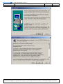
1. Install the “PORT95NT.EXE”, and restart the computer.
You must install the
at the first. The processing as follows:
The information contained in this document is the exclusive property of HannStar Display Corporation. It shall not be
disclosed,distributed or reproduced in whole or in part without written permission of HannStar Display Corporation.
HannStarDisplayCorp.
Document Title
HW191A _XY _HSM
Document No.
Page No.
Revision
46 46 / 72
07/08/03
The information contained in this document is the exclusive property of HannStar Display Corporation. It shall not be
disclosed,distributed or reproduced in whole or in part without written permission of HannStar Display Corporation.
HannStarDisplayCorp.
Document Title
HW191A _XY _HSM
Document No.
Page No.
Revision
47 47 / 72
07/08/03
The information contained in this document is the exclusive property of HannStar Display Corporation. It shall not be
disclosed,distributed or reproduced in whole or in part without written permission of HannStar Display Corporation.
HannStarDisplayCorp.
Document Title
HW191A _XY _HSM
Document No.
Page No.
Revision
48 48 / 72
07/08/03
The information contained in this document is the exclusive property of HannStar Display Corporation. It shall not be
disclosed,distributed or reproduced in whole or in part without written permission of HannStar Display Corporation.
HannStarDisplayCorp.
Document Title
HW191A _XY _HSM
Document No.
Page No.
Revision
49 49 / 72
07/08/03
Click
to complete the installation.
Note: After installation, you must restart the PC to take the setup to effect.
The information contained in this document is the exclusive property of HannStar Display Corporation. It shall not be
disclosed,distributed or reproduced in whole or in part without written permission of HannStar Display Corporation.
HannStarDisplayCorp.
Document Title
HW191A _XY _HSM
Document No.
Page No.
Revision
50 50 / 72
07/08/03
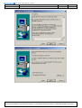
2. Install the “WinDDC_ setup”
Second, you must install the
. The processing as follows:
The information contained in this document is the exclusive property of HannStar Display Corporation. It shall not be
disclosed,distributed or reproduced in whole or in part without written permission of HannStar Display Corporation.
HannStarDisplayCorp.
Document Title
HW191A _XY _HSM
Document No.
Page No.
Revision
51 51 / 72
07/08/03
The information contained in this document is the exclusive property of HannStar Display Corporation. It shall not be
disclosed,distributed or reproduced in whole or in part without written permission of HannStar Display Corporation.
HannStarDisplayCorp.
Document Title
HW191A _XY _HSM
Document No.
Page No.
Revision
52 52 / 72
07/08/03
Click
to complete the installation.
3. Connect the DDC board as follow:
(Take philips 190B8 for example)
Connect to the
When you write analog
PC LPT
EDID, Connect this port
to the Philips 190B8’s
VGA port
When you write digital
EDID, Connect this port
to the Philips 190B8’s DVI
12V Input
port
Note: Pin5 of the VGA cable which connects to the monitor should be cut off.
The information contained in this document is the exclusive property of HannStar Display Corporation. It shall not be
disclosed,distributed or reproduced in whole or in part without written permission of HannStar Display Corporation.
HannStarDisplayCorp.
Document Title
HW191A _XY _HSM
Document No.
Page No.
Revision
53 53 / 72
07/08/03
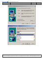
4. Take analog DDC write for example, as follow
a. Double-click
,appear as follow Figs:
The information contained in this document is the exclusive property of HannStar Display Corporation. It shall not be
disclosed,distributed or reproduced in whole or in part without written permission of HannStar Display Corporation.
HannStarDisplayCorp.
Document Title
HW191A _XY _HSM
Document No.
Page No.
Revision
54 54 / 72
07/08/03
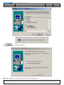
b. Click
.
c. Key 14 numbers in the Serial Number blank, then click “OK”. Now analog DDC Write completes, as follow.
The information contained in this document is the exclusive property of HannStar Display Corporation. It shall not be
disclosed,distributed or reproduced in whole or in part without written permission of HannStar Display Corporation.
HannStarDisplayCorp.
Document Title
HW191A _XY _HSM
Document No.
Page No.
Revision
55 55 / 72
07/08/03
Note: The way of digital DDC write is the same as analog DDC write.
HW191A EDID
Analog
128 bytes EDID Data (Hex):
00 01 02 03 04 05 06 07 08 09 10 11 12 13 14 15
0:
00 FF FF FF FF FF FF 00 22 64 91 89 00 00 00 00
16:
10 12 01 03 0A 29 1A 78 EA 9B B6 A4 53 4B 9D 24
32:
14 4F 54 BF EF 80 81 80 81 C0 81 40 71 4F 61 46
48:
90 4F 95 0F 01 01 9A 29 A0 D0 51 84 22 30 50 98
64:
36 00 98 FF 10 00 00 1E 00 00 00 FD 00 31 4B 1E
80:
53 0E 00 0A 20 20 20 20 20 20 00 00 00 FF 00 31
96:
32 33 34 35 36 37 38 39 30 31 32 33 00 00 00 FC
112: 00 48 61 6E 6E 73 2E 47 20 48 57 31 39 31 00 05
Decoded EDID data
<---Header--->
Header: 00 FF FF FF FF FF FF 00
The information contained in this document is the exclusive property of HannStar Display Corporation. It shall not be
disclosed,distributed or reproduced in whole or in part without written permission of HannStar Display Corporation.
HannStarDisplayCorp.
Document Title
HW191A _XY _HSM
Document No.
Page No.
Revision
56 56 / 72
07/08/03
<-x-Header-x->
<---Vendor/Product Identification--->
ID Manufacturer Name:
HSD
ID Product Code:
8991
ID Serial Number:
00000000
Week of Manufacture:
16
Year of Manufacture:
2008
<-x-Vendor/Product Identification-x->
<---EDID Structure Version/Revision--->
EDID Version#:
01
EDID Revision#:
03
<-x-EDID Structure Version/Revision-x->
<---Basic Display Parameters/Features--->
Video i/p definition:
Analog
Signal Level Standard:
0.700V/0.300V(0.700Vpp)
Setup:
Blank-to-Black not expected
Separate Sync Support:
Yes
Composite Sync Support: No
Sync. on green video supported:
Yes
Serration of the Vsync.Pulse is not required.
Max. H. Image Size :
41cm.
Max. V. Image Size :
26cm.
Display Gamma:
2.2
DPMS Features, Stand-by:
Yes.
DPMS Features, Suspend:
Yes.
DPMS Features, Active off:
Yes.
Display Type:
R/G/B color display.
Preferred Timing Mode:
Yes.
<---Basic Display Parameters/Features--->
<---Color Characteristics--->
Red x:
0.6425781250
Red y:
0.3251953125
Green x:
0.2978515625
Green y:
0.6162109375
Blue x:
0.1425781250
Blue y:
0.0810546875
White x:
0.3095703125
White y:
0.3310546875
<-x-Color Characteristics-x->
<---Established Timings--->
Established Timings 1: BF
The information contained in this document is the exclusive property of HannStar Display Corporation. It shall not be
disclosed,distributed or reproduced in whole or in part without written permission of HannStar Display Corporation.
HannStarDisplayCorp.
Document Title
HW191A _XY _HSM
Document No.
Page No.
Revision
57 57 / 72
07/08/03
-720x400 @70Hz VGA,IBM
-640x480 @60Hz VGA,IBM
-640x480 @67Hz Apple,Mac II
-640x480 @72Hz VESA
-640x480 @75Hz VESA
-800x600 @56Hz VESA
-800x600 @60Hz VESA
Established Timings 2: EF
-800x600 @72Hz VESA
-800x600 @75Hz VESA
-832x624 @75Hz Apple,Mac II
-1024x768 @60Hz VESA
-1024x768 @70Hz VESA
-1024x768 @75Hz VESA
-1280x1024 @75Hz VESA
Established Timings 3: 80
-1152x870 @75Hz Apple,Mac II
<-x-Established Timings-x->
<---Standard Timing Identification--->
-1280x1024
@60
-1280x720 @60
-1280x960 @60
-1152x864 @75
-1024x768 @66
-1400x1050
@75
-1440x900 @75
<-x-Standard Timing Identification-x->
<---Detailed Timing Descriptions--->
Detailed Timing:
1440x900 @ 60Hz.
<-x-Detailed Timing Descriptions-x->
<---Detailed Timing Descriptions--->
Detailed Timing: FD (Monitor limits)
Min. V. rate:
49Hz
Max. V. rate:
75Hz
Min. H. rate:
30KHz
Max. H. rate:
83KHz
Max. Pixel Clock:
140MHz
Detailed Timing: FF (Monitor SN) '1234567890123'
Detailed Timing:
FC (Monitor Name) 'Hanns.G HW191 '
<-x-Detailed Timing Descriptions-x->
Extension Flag:
Checksum:
00
05
The information contained in this document is the exclusive property of HannStar Display Corporation. It shall not be
disclosed,distributed or reproduced in whole or in part without written permission of HannStar Display Corporation.
HannStarDisplayCorp.
Document Title
HW191A _XY _HSM
Document No.
Page No.
Revision
58 58 / 72
07/08/03
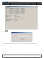
13. White- Balance, Luminance Adjustment
Approximately 30 minutes should be allowed for warm up before proceeding White-Balance adjustment.
1. How to do the Chroma-7120 MEM. Channel setting
A. Reference to chroma 7120 user guide
B. Use “SC” key and “NEXT” key to modify x,y,Y value and use “ID” key to modify the
TEXT description Following is the procedure to do white-balance adjust
2. Setting the color temp. you want
A. MEM.CHANNEL 3 (9300 color):
9300 color temp. parameter is x = 283 ±28, y = 297 ±28,Y=220cd/㎡
B. MEM.CHANNEL 4 (6500 color):
6500 color temp. parameter is x = 313±28, y = 329 ±28, Y=220cd/㎡
C. MEM.CHANNEL 9 (5500 color):
5500 color temp. parameter is x = 333±28, y = 348 ±28, Y=220cd/㎡
3. Enter into factory mode of HW191A
Turn on the power, press simultaneously the MENU and AUTO buttons, then the factory OSD will be at the left top of the
panel.
4. Bias adjustment:
Set the Contrast
to 70; Adjust the Brightness
to 100.
5. Gain adjustment:
Move cursor to “-F-” and press MENU key
A. Adjust 9300 color-temperature
1. Switch the Chroma-7120 to RGB-Mode (with press “MODE” button)
2. Switch the MEM. Channel to Channel 3 (with up or down arrow on chroma 7120)
3. The LCD-indicator on chroma 7120 will show x = 283 ±28, y = 297 ±28, Y=220cd/㎡
4. Adjust the RED of color 1 on factory window until chroma 7120 indicator reached the value R=100
5. Adjust the GREEN of color 1 on factory window until chroma 7120 indicator reached the value G=100
6. Adjust the BLUE of color 1 on factory window until chroma 7120 indicator reached the value B=100
7. Repeat above procedure (item 4,5,6) until chroma 7120 RGB value meet the tolerance =100±2
B. Adjust 6500 color-temperature
1. Switch the chroma-7120 to RGB-Mode (with press “MODE” button)
2. Switch the MEM.channel to Channel 4(with up or down arrow on chroma 7120)
3. The LCD-indicator on chroma 7120 will show x = 313 ±28, y = 329 ±28, Y=220cd/㎡
4. Adjust the RED of color 2 on factory window until chroma 7120 indicator reached the value R=100
5. Adjust the GREEN of color 2 on factory window until chroma 7120 indicator reachedthe value G=100
6. Adjust the BLUE of color 2 on factory window until chroma 7120 indicator reached the value B=100
7. Repeat above procedure (item 4,5,6) until chroma 7120 RGB value meet the tolerance =100±2
C. Adjust 5500 color-temperature
The information contained in this document is the exclusive property of HannStar Display Corporation. It shall not be
disclosed,distributed or reproduced in whole or in part without written permission of HannStar Display Corporation.
HannStarDisplayCorp.
Document Title
HW191A _XY _HSM
Document No.
Page No.
Revision
59 59 / 72
07/08/03
1. Switch the chroma-7120 to RGB-Mode (with press “MODE” button)
2. Switch the MEM.channel to Channel 9 (with up or down arrow on chroma 7120)
3. The LCD-indicator on chroma 7120 will show x = 333±28, y = 348 ±28, Y=220cd/㎡
4. Adjust the RED of color 3 on factory window until chroma 7120 indicator reached the value R=100
5. Adjust the GREEN of color 3 on factory window until chroma 7120 indicator reachedthe value G=100
6. Adjust the BLUE of color 3 on factory window until chroma 7120 indicator reached the value B=100
7. Repeat above procedure (item 4,5,6) until chroma 7120 RGB value meet the tolerance =100±2
D. Turn the Power-button off to quit from factory mode.
The information contained in this document is the exclusive property of HannStar Display Corporation. It shall not be
disclosed,distributed or reproduced in whole or in part without written permission of HannStar Display Corporation.
HannStarDisplayCorp.
Document Title
HW191A _XY _HSM
Document No.
Page No.
Revision
60 60 / 72
07/08/03
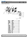
14.Monitor Exploded View
The information contained in this document is the exclusive property of HannStar Display Corporation. It shall not be
disclosed,distributed or reproduced in whole or in part without written permission of HannStar Display Corporation.
HannStarDisplayCorp.
Document Title
HW191A _XY _HSM
Document No.
Page No.
Revision
61 61 / 72
07/08/03
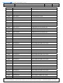
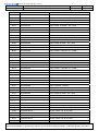
15. BOM List
T98HRDDTWNHZACE
Location
Part NO.
Description
040G 58162435A
P/N LABEL FOR MANUAL PE BAG
040G 58162461A
EPA LABEL
045G 77 3
PE PACKING
050G 600 1 W
WHITE STRAP
050G 600 2
HANDLE1
050G 600 3
HANDLE2
052G
1211 B
Conductive Tape 85mm *40mm *0.09mm
052G
1211527
Conductive Tape 75mm *45mm *0.08mm
052G6020 17
PROTECT FILM
E078
078G 457E01 Y
SPEAKER 4 OHM 2W 40*20MM 100MM
E08904
089G 173 56 4B
AUDIO CABLE
E08902
089G 715HAA D2
SIGNAL CABLE
E08901
089G420A18N IS
POWER CORD 32-D001922
E09504
095G8014 2TE01
HARNESS 2P-2P 480MM
E09503
095G8014 3TE01
HARNESS 3P-2P 100MM
E09502
095G801410WE13
HARNESS 10P-(6+4)P 340MM
E09501
095G8018 3TE12
WIRE HARNESS 30P-24P 185mm TONGFU
0D1G1730 8120
SCREW
0D1G1740 8120
SCREW
0M1G 130 6120
SCREW M3X6
0M1G 140 10225 CR3
SCREW
0M1G 930 4120
screw
0M1G 940 6 47 CR3
SCREW
705GH834038
ASS'Y
750GLH90GW122N000R
PANEL HSD190MGW1-A02 NJ HSD
AUPC8HA3
Audio Board G3137-1-X-X-1-080715
CBPC8HRDHZH1
Main Board G2498-1-2-X-6-080618
H15G0012HSD 1
MAIN FRAME
H26G 800850 1B
BARCODE
H33G0009 ZT 1B
OSD-BUTTON
H33G0010 1 1C
POWER LENS
H34G0018DAAA1B
BEZEL
H34G0019 ZT 1B
REAR COVER
H40G 19N85012A
HW191A ID LABEL
H40G 581850 3A
STICKER WARRANTY
H40G 58185010A
BEZEL BASIC VISTA LOGO
H41G780085026A
QSG
H44G9017 1
EPS
H44G9017 2
EPS
E750
LABEL
The information contained in this document is the exclusive property of HannStar Display Corporation. It shall not be
disclosed,distributed or reproduced in whole or in part without written permission of HannStar Display Corporation.
HannStarDisplayCorp.
Document Title
HW191A _XY _HSM
Document No.
Page No.
Revision
62 62 / 72
07/08/03
H44G9017850 2A
HW TW CARTON
H45G 76 28 HS
PE BAG FOR MANUAL
H45G 87 1HS1
EPE COVER
H45G 87 4HS2
PE BAG FOR BASE
H70G1600850 6A
CD MANUAL
U402
056G 158501
IC AS431AN-E1 SOT23
U501
056G 562701
SCALER IC RTD2025L QFN-48
U201
056G 585 4A
IC AP1117E33L-13
U401
056G1125701 X
IC MCU RTD2120L-LF REALTEK
U403
056G1133 56
M24C16-WMN6TP
Q501
057G 417 22 T
TRA KN2907AS -60V/-0.6A SOT-23
Q502
057G 417 22 T
TRA KN2907AS -60V/-0.6A SOT-23
Q602
057G 417517
LMBT3906LT1G SOT-23 BY LRC
Q205
057G 417517
LMBT3906LT1G SOT-23 BY LRC
Q204
057G 417517
LMBT3906LT1G SOT-23 BY LRC
Q202
057G 417518
LMBT3904LT1G SOT-23 BY LRC
Q401
057G 417518
LMBT3904LT1G SOT-23 BY LRC
Q601
057G 763 1
A03401 SOT23 BY AOS(A1)
R302
061G0402000
RST CHIP MAX 0R05 1/16W
R427
061G0402000
RST CHIP MAX 0R05 1/16W
R429
061G0402000
RST CHIP MAX 0R05 1/16W
R409
061G0402101
RST CHIPR 100 OHM +-5% 1/16W
R410
061G0402101
RST CHIPR 100 OHM +-5% 1/16W
R420
061G0402101
RST CHIPR 100 OHM +-5% 1/16W
R422
061G0402101
RST CHIPR 100 OHM +-5% 1/16W
R430
061G0402101
RST CHIPR 100 OHM +-5% 1/16W
R432
061G0402101
RST CHIPR 100 OHM +-5% 1/16W
R433
061G0402101
RST CHIPR 100 OHM +-5% 1/16W
R434
061G0402101
RST CHIPR 100 OHM +-5% 1/16W
R435
061G0402101
RST CHIPR 100 OHM +-5% 1/16W
R408
061G0402101
RST CHIPR 100 OHM +-5% 1/16W
R301
061G0402101
RST CHIPR 100 OHM +-5% 1/16W
R303
061G0402101
RST CHIPR 100 OHM +-5% 1/16W
R306
061G0402101
RST CHIPR 100 OHM +-5% 1/16W
R308
061G0402101
RST CHIPR 100 OHM +-5% 1/16W
R309
061G0402101
RST CHIPR 100 OHM +-5% 1/16W
R311
061G0402101
RST CHIPR 100 OHM +-5% 1/16W
R312
061G0402101
RST CHIPR 100 OHM +-5% 1/16W
R313
061G0402101
RST CHIPR 100 OHM +-5% 1/16W
R315
061G0402101
RST CHIPR 100 OHM +-5% 1/16W
R402
061G0402102
RST CHIPR 1 KOHM +-5% 1/16W
R424
061G0402102
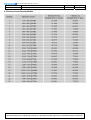
RST CHIPR 1 KOHM +-5% 1/16W
R453
061G0402102
RST CHIPR 1 KOHM +-5% 1/16W
R601
061G0402103
RST CHIPR 10 KOHM +-5% 1/16W
The information contained in this document is the exclusive property of HannStar Display Corporation. It shall not be
disclosed,distributed or reproduced in whole or in part without written permission of HannStar Display Corporation.
HannStarDisplayCorp.
Document Title
HW191A _XY _HSM
Document No.
Page No.
Revision
63 63 / 72
07/08/03
R438
061G0402103
RST CHIPR 10 KOHM +-5% 1/16W
R436
061G0402103
RST CHIPR 10 KOHM +-5% 1/16W
R425
061G0402103
RST CHIPR 10 KOHM +-5% 1/16W
R416
061G0402103
RST CHIPR 10 KOHM +-5% 1/16W
R404
061G0402103
RST CHIPR 10 KOHM +-5% 1/16W
R213
061G0402103
RST CHIPR 10 KOHM +-5% 1/16W
R210
061G0402103
RST CHIPR 10 KOHM +-5% 1/16W
R207
061G0402121
RST CHIP 120R 1/16W 5%
R208
061G0402121
RST CHIP 120R 1/16W 5%
R201
061G0402201
RST CHIP 200R 1/16W 5%
R413
061G0402202
RST CHIP 2K 1/16W 5%
R414
061G0402202
RST CHIP 2K 1/16W 5%
R428
061G0402220
RST CHIPR 22 OHM +-5% 1/16W
R426
061G0402220
RST CHIPR 22 OHM +-5% 1/16W
R304
061G0402222
RST CHIPR 2.2 KOHM +-5% 1/16W
R305
061G0402222
RST CHIPR 2.2 KOHM +-5% 1/16W
R401
061G0402392
RST CHIP 3.9K 1/16W 5%
R403
061G0402392
RST CHIP 3.9K 1/16W 5%
R437
061G0402392
RST CHIP 3.9K 1/16W 5%
R605
061G0402472
RST CHIPR 4.7 KOHM +-5% 1/16W
R451
061G0402472
RST CHIPR 4.7 KOHM +-5% 1/16W
R412
061G0402472
RST CHIPR 4.7 KOHM +-5% 1/16W
R411
061G0402472
RST CHIPR 4.7 KOHM +-5% 1/16W
R407
061G0402472
RST CHIPR 4.7 KOHM +-5% 1/16W
R406
061G0402472
RST CHIPR 4.7 KOHM +-5% 1/16W
R405
061G0402472
RST CHIPR 4.7 KOHM +-5% 1/16W
R202
061G0402472
RST CHIPR 4.7 KOHM +-5% 1/16W
R604
061G0402473
RST CHIPR 47 KOHM +-5% 1/16W
R415
061G0402682
RST CHIP 6K8 1/16W 5%
R431
061G0402682
RST CHIP 6K8 1/16W 5%
R307
061G0402750
RST CHIPR 75 OHM +-5% 1/16W
R310
061G0402750
RST CHIPR 75 OHM +-5% 1/16W
R314
061G0402750
RST CHIPR 75 OHM +-5% 1/16W
R602
061G0805331
RST CHIPR 330 OHM +-5% 1/8W
C401
065G0402100 31
CAP 0402 10PF J 50V NPO
C411
065G0402100 31
CAP 0402 10PF J 50V NPO
C602
065G0402103 22
CHIP 0.01UF 25V X7R
C603
065G0402104 15
MLCC 0402 0.1UF K 16V X5R
C507
065G0402104 15
MLCC 0402 0.1UF K 16V X5R
C506
065G0402104 15
MLCC 0402 0.1UF K 16V X5R
C503
065G0402104 15
MLCC 0402 0.1UF K 16V X5R
C501
065G0402104 15
MLCC 0402 0.1UF K 16V X5R
C410
065G0402104 15
MLCC 0402 0.1UF K 16V X5R
C406
065G0402104 15
MLCC 0402 0.1UF K 16V X5R
The information contained in this document is the exclusive property of HannStar Display Corporation. It shall not be
disclosed,distributed or reproduced in whole or in part without written permission of HannStar Display Corporation.
HannStarDisplayCorp.
Document Title
HW191A _XY _HSM
Document No.
Page No.
Revision
64 64 / 72
07/08/03
C404
065G0402104 15
MLCC 0402 0.1UF K 16V X5R
C201
065G0402104 15
MLCC 0402 0.1UF K 16V X5R
C204
065G0402104 15
MLCC 0402 0.1UF K 16V X5R
C205
065G0402104 15
MLCC 0402 0.1UF K 16V X5R
C206
065G0402104 15
MLCC 0402 0.1UF K 16V X5R
C209
065G0402104 15
MLCC 0402 0.1UF K 16V X5R
C210
065G0402104 15
MLCC 0402 0.1UF K 16V X5R
C315
065G0402104 15
MLCC 0402 0.1UF K 16V X5R
C403
065G0402104 15
MLCC 0402 0.1UF K 16V X5R
C402
065G0402105 A5
CAP 0402 1UF K 10V X5R
C412
065G0402105 A5
CAP 0402 1UF K 10V X5R
C302
065G0402220 31
CHIP 22PF 50V NPO
C303
065G0402220 31
CHIP 22PF 50V NPO
C311
065G0402473 12
CHIP 0.047uF 16V X7R
C309
065G0402473 12
CHIP 0.047uF 16V X7R
C307
065G0402473 12
CHIP 0.047uF 16V X7R
C306
065G0402473 12
CHIP 0.047uF 16V X7R
C304
065G0402473 12
CHIP 0.047uF 16V X7R
C301
065G0402473 12
CHIP 0.047uF 16V X7R
C305
065G0402509 31
CHIP 5pF 50V NPO
C308
065G0402509 31
CHIP 5pF 50V NPO
C310
065G0402509 31
CHIP 5pF 50V NPO
FB601
071G 56K121 M
CHIP BEAD
FB503
071G 56K121 M
CHIP BEAD
FB502
071G 56K121 M
CHIP BEAD
FB201
071G 56K121 M
CHIP BEAD
FB301
071G 59K190 B
19 OHM BEAD
FB302
071G 59K190 B
19 OHM BEAD
FB303
071G 59K190 B
19 OHM BEAD
D402
093G 64 42 PP
BAV70 SOT-23
D301
093G 6433S
DIODE BAV99 SEMTECH
D302
093G 6433S
DIODE BAV99 SEMTECH
D303
093G 6433S
DIODE BAV99 SEMTECH
ZD301
093G 39S501 T
LUDZS5.6BT1G BY LRC
ZD302
093G 39S501 T
LUDZS5.6BT1G BY LRC
ZD303
093G 39S501 T
LUDZS5.6BT1G BY LRC
ZD304
093G 39S501 T
LUDZS5.6BT1G BY LRC
ZD305
093G 39S501 T
LUDZS5.6BT1G BY LRC
ZD307
093G 39S501 T
LUDZS5.6BT1G BY LRC
715G2498 1 2
MAIN BOARD PCB
KEPC8HA1
KEY BOARDG3218-1-X-X-1-080715
PWPC8942CHD1
POWER G2594-2-X-X-7-080618
Q40G 58170931A
HT POT LABEL
Q40G000260811A
Basic label
The information contained in this document is the exclusive property of HannStar Display Corporation. It shall not be
disclosed,distributed or reproduced in whole or in part without written permission of HannStar Display Corporation.
HannStarDisplayCorp.
Document Title
HW191A _XY _HSM
Document No.
Page No.
Revision
65 65 / 72
07/08/03
0Q1G 130 8120
SCREW 42A9930011
0Q1G1740 12120
SCREW
AQ1G1740 12120
SCREW
H12G6118 2
PORON FOOT
H15G0013 1
BASE BRACBET
H34G0020 ZT 1B
BASE
H34G0021 ZT 1B
STAND COVER FRONT
H34G0022 ZT 1B
STAND COVER REAR
H37G0007 1
HINGE
CN102
033G3802 4
WAFER EH-4
CN103
033G3802 4B Y
CN101
088G 30214K
PHONE JACK 5PIN
Q90G6258 2
HEAT SINK
056G 616 37
IC TPA6021A4NE4 2W*2 PDIP-20
U101
W
WAFER
CN202
033G3802 6B Y
L
WAFER
CN201
033G3802 9B Y
W
WAFER
CN601
033G8027 24 H
CONN W TO B12P*2 P*2.0 4505-2
040G 45762412B
CBPC LABEL
R507
061G152M33964L
RST MOFR 3.3 OHM +-5% 2WS
C405
067G 3151007KV
ELCAP 10UF M 50V 105℃ KINGNICHI
C203
067G 3151014KV
EC 105℃ CAP 100uF M 25V
C202
067G 3151014KV
EC 105℃ CAP 100uF M 25V
C604
067G 3154704KV
ELCAP 47UF M 25V 105℃ KINGNICHI
C505
067G315V220 7K
CAP 105℃ 22UF M 50V
CN301
088G 35315F HD
D-SUB CONN F ATTACHED SCREW
X401
093G 22 45 H
24MHZ/30PF/49US
GND1
009G6005 1
GROUND TERMINAL
GND2
009G6005 1
GROUND TERMINAL
CN804
033G8021 2E F
WAFER
CN803
033G8021 2E F
WAFER
CN802
033G8021 2E F
WAFER
CN801
033G8021 2E F
WAFER
040G 45762412B
CBPC LABEL
IC902
056G 139 3A
IC PC123Y22FZ0F
NR901
061G 58100 WD
RST NTCR 10 OHM +-20% 5A THINKING
R907
061G152M15164L
RST MOFR 150 OHM +-5% 2WS
C909
063G107K474 US
0.47UF +-10%
C812
065G 6J1006ET
10PF 5% SL 6KV
C801
065G 6J1006ET
10PF 5% SL 6KV
C901
065G305M1022EM
Y2 1000PF +-20% 250VAC
C902
065G305M1022EM
Y2 1000PF +-20% 250VAC
C903
065G306M1022BP
1000PF Y1.CAP
C900
065G306M2222BP
2200PF +-20% 250VAC
C907
067G 40Z10115K
CAP 105℃ 100UF M 450V
The information contained in this document is the exclusive property of HannStar Display Corporation. It shall not be
disclosed,distributed or reproduced in whole or in part without written permission of HannStar Display Corporation.
HannStarDisplayCorp.
Document Title
HW191A _XY _HSM
Document No.
Page No.
Revision
66 66 / 72
07/08/03
C926
067G215P1023AV
CAP 105℃ 1000UF M 16V
C927
067G215P1023AV
CAP 105℃ 1000UF M 16V
C925
067G215P4714AV
CAP 105℃ 470UF M 25V
C923
067G215P4714AV
CAP 105℃ 470UF M 25V
C922
067G215P4714AV
CAP 105℃ 470UF M 25V
C811
067G215P4714AV
CAP 105℃ 470UF M 25V
C805
067G215P4714AV
CAP 105℃ 470UF M 25V
C924
067G215P6814AV
CAP 105C 680UF M 25V
L902
073G 174 65 H
LINE FILTER
L901
073G 174 76 H
FILTER
L921
073G 253 91 H
CHOKE COIL
L922
073G 253 91 H
CHOKE COIL
T901
080GL17T 33 N2
XFMR POWER 550uH YUVA
PT801
080GL17T 40 DN
X'FMR TK.2001U.101
PT802
080GL17T 40 DN
X'FMR TK.2001U.101
CN901
087G 501 32 DL
AC SOCKET DIP 3PIN+2PIN GROUND
CN902
095G 82510TE03
HARNESS 10P-(9+4)P 200mm
705GQ793015
D921 ASS'Y
705GQ9KP 57001
Q900 ASS"Y
705GQ9KP 93001
D920 ASS"Y
HS4
Q85G0053 1 S
shield
BD901
093G 50460 28
BRIDGE DIODE KBP208G LITEON
R101
061G0603103
RST CHIPR 10 KOHM +-5% 1/10W
R102
061G0603103
RST CHIPR 10 KOHM +-5% 1/10W
R103
061G0603103
RST CHIPR 10 KOHM +-5% 1/10W
R104
061G0603103
RST CHIPR 10 KOHM +-5% 1/10W
R105
061G0603103
RST CHIPR 10 KOHM +-5% 1/10W
R107
061G0603622
RST CHIPR 6.2 KOHM +-5% 1/10W
R106
061G0603622
RST CHIPR 6.2 KOHM +-5% 1/10W
RJ001
061G0805000
RST CHIP MAX 0R05 1/8W
RJ002
061G0805000
RST CHIP MAX 0R05 1/8W
RJ003
061G0805000
RST CHIP MAX 0R05 1/8W
C111
065G0603101 31
CER1 0603 NP0 50V 100P PM5 R
C110
065G0603101 31
CER1 0603 NP0 50V 100P PM5 R
C106
065G0603474 12
MLCC 0603 0.47UF K 16V X7R
C107
065G0603474 12
MLCC 0603 0.47UF K 16V X7R
C103
065G0603474 12
MLCC 0603 0.47UF K 16V X7R
C105
065G0603474 12
MLCC 0603 0.47UF K 16V X7R
C102
065G0603474 12
MLCC 0603 0.47UF K 16V X7R
C101
065G0603474 12
MLCC 0603 0.47UF K 16V X7R
C109
065G0805105 22
CAP CHIP 0805 1uF K 25V X7R
CN003
033G8032 2W L
WAFER 1.25 2P
CN002
033G8032 3W L
WAFER 1.25 3P
CN001
033G803210W L
WAFER 1.25 10P
The information contained in this document is the exclusive property of HannStar Display Corporation. It shall not be
disclosed,distributed or reproduced in whole or in part without written permission of HannStar Display Corporation.
HannStarDisplayCorp.
Document Title
HW191A _XY _HSM
Document No.
Page No.
Revision
67 67 / 72
07/08/03
R003
061G0603180 1F
RST CHIPR 1.8 KOHM +-1% 1/10W
R004
061G0603180 1F
RST CHIPR 1.8 KOHM +-1% 1/10W
R002
061G0603300 1F
RST CHIPR 3 KOHM +-1% 1/10W
R005
061G0603300 1F
RST CHIPR 3 KOHM +-1% 1/10W
C010
065G0603104 32
CHIP 0.1UF 50V X7R
C009
065G0603104 32
CHIP 0.1UF 50V X7R
C008
065G0603104 32
CHIP 0.1UF 50V X7R
C007
065G0603104 32
CHIP 0.1UF 50V X7R
SW001
077G 607 4 TO
TACT SW 5P3.1 180TS-1157ALNP-F
SW002
077G 607 4 TO
TACT SW 5P3.1 180TS-1157ALNP-F
SW003
077G 607 4 TO
TACT SW 5P3.1 180TS-1157ALNP-F
SW004
077G 607 4 TO
TACT SW 5P3.1 180TS-1157ALNP-F
SW005
077G 607 4 TO
TACT SW 5P3.1 180TS-1157ALNP-F
LED001
081G 14501 GP
LED GPTD1210YGC3-HB GUANGPU
715G3218 1
KEY BOARD PCB
HS2
090G6263 1
HEAT SINK
D921
093G 60526
SCHOTTKY MBRF1060CT ITO-220AB
0M1G1730 8120
SCREW
Q900
057G 667 21
STP10NK70ZFP
HS1
090G6264 1
HEAT SINK
0M1G1730 8120
SCREW
HS5
090G6241 1
GP
HEAT SINK
D920
093G 60276
DIODE SBT150-10LST SANYO
0M1G1730 8120
SCREW
IC801
056G 379 22
IC TL494IDR SOIC-16
IC901
056G 379 61
LD7575PS SOP-8
Q902
057G 417 4
PMBS3904/PHILIPS-SMT(04)
Q803
057G 417 4
PMBS3904/PHILIPS-SMT(04)
Q807
057G 417 4
PMBS3904/PHILIPS-SMT(04)
Q810
057G 417 4
PMBS3904/PHILIPS-SMT(04)
Q811
057G 417 4
PMBS3904/PHILIPS-SMT(04)
Q806
057G 417 6
PMBS3906/PHILIPS-SMT(06)
Q805
057G 417 6
PMBS3906/PHILIPS-SMT(06)
Q812
057G 759 2
RK7002
Q808
057G 759 2
RK7002
Q801
057G 760 4B
PDTA144WK SOT346
Q802
057G 760 5B
PDTC144WK SOT346
Q809
057G 763 6
AO4828L
Q804
057G 763 6
AO4828L
R832
061G0603000
RST CHIP MAX 0R05 1/10W
R830
061G0603000
RST CHIP MAX 0R05 1/10W
R804
061G0603000
RST CHIP MAX 0R05 1/10W
R801
061G0603000
RST CHIP MAX 0R05 1/10W
R849
061G0603100 1F
RST CHIPR 1 KOHM +-1% 1/10W
The information contained in this document is the exclusive property of HannStar Display Corporation. It shall not be
disclosed,distributed or reproduced in whole or in part without written permission of HannStar Display Corporation.
HannStarDisplayCorp.
Document Title
HW191A _XY _HSM
Document No.
Page No.
Revision
68 68 / 72
07/08/03
R848
061G0603100 1F
RST CHIPR 1 KOHM +-1% 1/10W
R835
061G0603100 1F
RST CHIPR 1 KOHM +-1% 1/10W
R834
061G0603100 1F
RST CHIPR 1 KOHM +-1% 1/10W
R827
061G0603100 1F
RST CHIPR 1 KOHM +-1% 1/10W
R807
061G0603100 1F
RST CHIPR 1 KOHM +-1% 1/10W
R806
061G0603100 1F
RST CHIPR 1 KOHM +-1% 1/10W
R853
061G0603100 2F
RST CHIPR 10K OHM +-1% 1/10W
R852
061G0603100 2F
RST CHIPR 10K OHM +-1% 1/10W
R840
061G0603100 2F
RST CHIPR 10K OHM +-1% 1/10W
R838
061G0603100 2F
RST CHIPR 10K OHM +-1% 1/10W
R831
061G0603100 2F
RST CHIPR 10K OHM +-1% 1/10W
R833
061G0603100 2F
RST CHIPR 10K OHM +-1% 1/10W
R824
061G0603100 2F
RST CHIPR 10K OHM +-1% 1/10W
R819
061G0603100 2F
RST CHIPR 10K OHM +-1% 1/10W
R808
061G0603100 2F
RST CHIPR 10K OHM +-1% 1/10W
R813
061G0603101
RST CHIPR 100 OHM +-5% 1/10W
R823
061G0603103
RST CHIPR 10 KOHM +-5% 1/10W
R836
061G0603105
RST CHIPR 1M OHM +-5% 1/10W
R821
061G0603105
RST CHIPR 1M OHM +-5% 1/10W
R841
061G0603150 1F
RST CHIPR 1.5 KOHM +-1% 1/10W
R839
061G0603150 1F
RST CHIPR 1.5 KOHM +-1% 1/10W
R812
061G0603150 1F
RST CHIPR 1.5 KOHM +-1% 1/10W
R811
061G0603150 1F
RST CHIPR 1.5 KOHM +-1% 1/10W
R847
061G0603220
RST CHIPR 22 OHM +-5% 1/10W
R844
061G0603220
RST CHIPR 22 OHM +-5% 1/10W
R845
061G0603220
RST CHIPR 22 OHM +-5% 1/10W
R846
061G0603220
RST CHIPR 22 OHM +-5% 1/10W
R803
061G0603362
RST CHIPR 3.6 KOHM +-5% 1/10W
R815
061G0603470 2F
RST CHIPR 47 KOHM +-1% 1/10W
R828
061G0603470 2F
RST CHIPR 47 KOHM +-1% 1/10W
R842
061G0603470 2F
RST CHIPR 47 KOHM +-1% 1/10W
R805
061G0603472
RST CHIPR 4.7K OHM +-5% 1/10W
R822
061G0603473
RST CHIPR 47 KOHM +-5% 1/10W
R820
061G0603564
RST CHIPR 560 KOHM +-5% 1/10W
R816
061G0603680 2F
RST CHIPR 68K
OHM +-1% 1/10W
R829
061G0603680 2F
RST CHIPR 68K
OHM +-1% 1/10W
R817
061G0603683
RST CHIPR 68K
OHM +-5% 1/10W
R814
061G0603750 2F
RST CHIPR 75KOHM +-1% 1/10W
R930
061G0805100 1F
RST CHIPR 1K
OHM +-1% 1/8W
R928
061G0805100 1F
RST CHIPR 1K
OHM +-1% 1/8W
R927
061G0805100 1F
RST CHIPR 1K
OHM +-1% 1/8W
R925
061G0805100 1F
RST CHIPR 1K
OHM +-1% 1/8W
R913
061G0805100 1F
RST CHIPR 1K
OHM +-1% 1/8W
R923
061G0805100 2F
RST CHIPR 10KOHM +-1% 1/8W
The information contained in this document is the exclusive property of HannStar Display Corporation. It shall not be
disclosed,distributed or reproduced in whole or in part without written permission of HannStar Display Corporation.
HannStarDisplayCorp.
Document Title
HW191A _XY _HSM
Document No.
Page No.
Revision
69 69 / 72
07/08/03
R915
061G0805100 2F
RST CHIPR 10KOHM +-1% 1/8W
R911
061G0805100 3F
RST CHIPR 100KOHM +-1% 1/8W
R802
061G0805101
1ST CHIPR 100
OHM +-5% 1/8W
R903
061G0805102
RST CHIPR 1K
OHM +-5% 1/8W
R826
061G0805180 3F
RST CHIPR 180 KOHM +-1% 1/8W
R929
061G0805240 1F
RST CHIPR 2.4K OHM +-1% 1/8W
R926
061G0805330 2F
RST CHIPR 33K OHM +-1% 1/8W
R924
061G0805360 1F
RST CHIPR 3.6K OHM +-1% 1/8W
R922
061G0805471
RST CHIPR 470 OHM +-5% 1/8W
R908
061G0805471
RST CHIPR 470 OHM +-5% 1/8W
R825
061G0805510 2F
RST CHIPR 51K OHM +-1% 1/8W
J813
061G1206000
RST CHIP MAX 0R05 1/4W
J818
061G1206000
RST CHIP MAX 0R05 1/4W
J907
061G1206000
RST CHIP MAX 0R05 1/4W
J908
061G1206000
RST CHIP MAX 0R05 1/4W
J814
061G1206000
RST CHIP MAX 0R05 1/4W
J815
061G1206000
RST CHIP MAX 0R05 1/4W
J816
061G1206000
RST CHIP MAX 0R05 1/4W
J807
061G1206000
RST CHIP MAX 0R05 1/4W
F902
061G1206000
RST CHIP MAX 0R05 1/4W
R912
061G1206100
RST CHIPR 10
ZD801
061G1206103
RST CHIPR 10K OHM +-5% 1/4W
R931
061G1206103
RST CHIPR 10K OHM +-5% 1/4W
R905
061G1206103
RST CHIPR 10K OHM +-5% 1/4W
R837
061G1206150
RST CHIPR 15 OHM +-5% 1/4W
R810
061G1206150
RST CHIPR 15 OHM +-5% 1/4W
R850
061G1206150
RST CHIPR 15 OHM +-5% 1/4W
R851
061G1206150
RST CHIPR 15 OHM +-5% 1/4W
R910
061G1206229
RST CHIPR 2.2 OHM +-5% 1/4W
R900
061G1206334
RST CHIPR 330KOHM +-5% 1/4W
R901
061G1206334
RST CHIPR 330KOHM +-5% 1/4W
R902
061G1206334
RST CHIPR 330KOHM +-5% 1/4W
R956
061G1206470
RST CHIPR 47 OHM +-5% 1/4W
R955
061G1206470
RST CHIPR 47 OHM +-5% 1/4W
R954
061G1206470
RST CHIPR 47 OHM +-5% 1/4W
R953
061G1206470
RST CHIPR 47 OHM +-5% 1/4W
R952
061G1206470
RST CHIPR 47 OHM +-5% 1/4W
R951
061G1206470
RST CHIPR 47 OHM +-5% 1/4W
C904
065G0603102 32
1000PF +-10% 50V X7R
C814
065G0603104 22
CAP CHIP 0603 0.1UF K 25V X7R
C810
065G0603104 22
CAP CHIP 0603 0.1UF K 25V X7R
C807
065G0603104 22
CAP CHIP 0603 0.1UF K 25V X7R
C804
065G0603104 22
CAP CHIP 0603 0.1UF K 25V X7R
C806
065G0603105 22
CHIP 1UF 25V X7R 0603
OHM +-5% 1/4W
The information contained in this document is the exclusive property of HannStar Display Corporation. It shall not be
disclosed,distributed or reproduced in whole or in part without written permission of HannStar Display Corporation.
HannStarDisplayCorp.
Document Title
HW191A _XY _HSM
Document No.
Page No.
Revision
70 70 / 72
07/08/03
C802
065G0603105 22
CHIP 1UF 25V X7R 0603
C813
065G0603222 32
CHIP 2200PF 50V X7R
C815
065G0603222 32
CHIP 2200PF 50V X7R
C817
065G0603222 32
CHIP 2200PF 50V X7R
C818
065G0603222 32
CHIP 2200PF 50V X7R
C928
065G0805104 32
CAP CHIP 0805 0.1uF K 50V X7R
C929
065G0805104 32
CAP CHIP 0805 0.1uF K 50V X7R
C930
065G0805104 32
CAP CHIP 0805 0.1uF K 50V X7R
C931
065G0805104 32
CAP CHIP 0805 0.1uF K 50V X7R
C916
065G0805104 32
CAP CHIP 0805 0.1uF K 50V X7R
C912
065G0805104 32
CAP CHIP 0805 0.1uF K 50V X7R
C824
065G0805104 32
CAP CHIP 0805 0.1uF K 50V X7R
C823
065G0805104 32
CAP CHIP 0805 0.1uF K 50V X7R
C822
065G0805152 32
CHIP 1500PF 50V X7R 0805
C821
065G0805152 32
CHIP 1500PF 50V X7R 0805
C816
065G0805152 32
CHIP 1500PF 50V X7R 0805
C803
065G0805152 32
CHIP 1500PF 50V X7R 0805
C913
065G0805221 31
CAP CHIP 0805 220PF J 50V NPO
C809
065G080522131G
CAP CHIP 0805 220PF G 50V NPO
C808
065G0805225 12
CAP CHIP 0805 2.2UF K 16V X7R
C914
065G0805471 31
CHIP 470PF 50V NPO
D806
093G 64 38 P
BAW56
D808
093G 64 38 P
BAW56
D810
093G 6433S
DIODE BAV99 SEMTECH
D809
093G 6433S
DIODE BAV99 SEMTECH
D802
093G 6433S
DIODE BAV99 SEMTECH
D801
093G 6433S
DIODE BAV99 SEMTECH
ZD922
093G 39S 25 T
RLZ5.1B LLDS
ZD921
093G 39S 40 T
RLZ 13B LLDS
ZD920
093G 39S 40 T
RLZ 13B LLDS
D916
093G 64S511SEM
1N4148W
D915
093G 64S511SEM
1N4148W
D910
093G 64S511SEM
1N4148W
D813
093G 64S511SEM
1N4148W
D812
093G 64S511SEM
1N4148W
D811
093G 64S511SEM
1N4148W
D807
093G 64S511SEM
1N4148W
D803
093G 64S511SEM
1N4148W
C108
067G215Y1007KT
KY50VB10M-TP5 5*11.5
C104
067G215Y1014KT
EC CAP.105 度
715G3137 1
AUDIO BOARD PCB
NR901
006G 31 4
1.7MM RIVET
CN901
006G 31500
EYELET
T901
006G 31502
1.5MM RIVET
The information contained in this document is the exclusive property of HannStar Display Corporation. It shall not be
disclosed,distributed or reproduced in whole or in part without written permission of HannStar Display Corporation.
HannStarDisplayCorp.
Document Title
HW191A _XY _HSM
Document No.
Page No.
Revision
71 71 / 72
07/08/03
IC903
056G 158 10 T
IC AS431AZTR-E1 TO-92
R909
061G152M10452T
RST MOFR 100KOHM +-5% 2WS
R916
061G152M43852T
RST MOF 0R43 5% 2W
C910
065G 2K152 1T6921
1.5NF/2KV Y5P +-10%
C921
065G517K102 5T
1000PF 10% Y5P 500V
C920
065G517K102 5T
1000PF 10% Y5P 500V
C911
067G 2152207NT
KY50VB22M-TP5 5*11
FB901
071G 55 29
FERRITE BEAD
FB903
071G 55 29
FERRITE BEAD
F901
084G 56 4W
FUSE 4.0A 250V
D901
093G 6038T52T
FR103
D900
093G1100 1152T
DIODE PR1007R 1A/1000V DO-41
715G2594 2
POWER BOARD PCB
The information contained in this document is the exclusive property of HannStar Display Corporation. It shall not be
disclosed,distributed or reproduced in whole or in part without written permission of HannStar Display Corporation.
HannStarDisplayCorp.
Document Title
HW191A _XY _HSM
Document No.
Page No.
Revision
72 72 / 72
07/08/03
16. DIFFERENT PARTS LIST
Diversity of T98HRDDBWNZHACE Compared with T98HRDDTWNHZACE
Location
E08901
Part No.
Description
089G421A18N IS
POWER CORD/32-D022217(与 TPV 共用)
H34G0018 ASA1B
BEZEL
H41G780085017B
EU-WARRANTY CARD
H44G9017850 3A
W EU CARTON
Q40G0002850 3A
Seal label
Diversity of T98HRDDYWNHZACE Compared with T98HRDDTWNHZACE
Location
E08901
Part No.
Description
040G 45760819A
DATE/MODEL LABEL
089G414A18N IS
POWER CORD 32E1818021(与 TPV 共用)
H40G 581850 6A
PASS LABEL
H41G780085023B
warranty card HSG CN
H44G9017850 1A
HW PRC CARTON
H45G 87 2004
OUT PE BAG
Diversity of T98HRDDKWNHZACE Compared with T98HRDDTWNHZACE
Location
E08901
Part No.
Description
089G402A18N YH
POWER CORD(32-D022438)(美規)
H40G 58185012B
机器防拆标签
H41G780085018B
USA-warranty
H44G9017850 3A
W EU CARTON
The information contained in this document is the exclusive property of HannStar Display Corporation. It shall not be
disclosed,distributed or reproduced in whole or in part without written permission of HannStar Display Corporation.