1
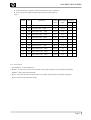
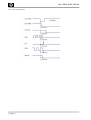
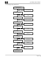
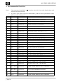
Service Manual
15-inch LCD Monitor
vf15 / FP15 / f1523 / FP5315
Service Manual Versions and Revision
N o.
Ve rs ion
R e le as e D ate
R e vis ion
1.
1.0
Mar 17, 2003
O riginal release
Copyright
Trademarks
Copyright 2003 LiteOn Technology Corp.
LiteOn is a registered trademark of LiteOn
Technology Corp.
All Rights Reserved
This manual may not, in whole or in part, be
copied, photocopied, reproduced, translated, or
converted to any electronic or machine readable
form without prior written permission of LiteOn
Technology Corp.
vf15 / FP15 / f1523 / FP5315 Service Manual.
All other trademarks are the property of their
respective owners.
vf15 / FP15 / f1523 / FP5315
1) Circuit
1.
Power board operation therory ---------------------------------------------------------------------------------------------- 3
2.
Inverter -------------------------------------------------------------------------------------------------------------------------- 4
3.
Power supply ------------------------------------------------------------------------------------------------------------------- 5
4.
On-screen circuit--------------------------------------------------------------------------------------------------------------- 5
5.
Video input circuit ------------------------------------------------------------------------------------------------------------- 5
6.
Definition converter LSI peripheral circuit --------------------------------------------------------------------------------- 5
7.
System reset, LED control circuit -------------------------------------------------------------------------------------------- 5
8.
E2PROM for PNP --------------------------------------------------------------------------------------------------------------- 6
9.
E2PROM ------------------------------------------------------------------------------------------------------------------------- 6
10. CPU circuit ---------------------------------------------------------------------------------------------------------------------- 6
10.1 Dection of POWER switch status ------------------------------------------------------------------------------------- 6
10.2 Display mode identification -------------------------------------------------------------------------------------------- 6
10.3 User control --------------------------------------------------------------------------------------------------------------- 7
10.4 Control of identification converter LSI (IC306) ---------------------------------------------------------------------- 8
10.5 Power ON sequence ----------------------------------------------------------------------------------------------------- 9
10.6 Power OFF sequence -------------------------------------------------------------------------------------------------- 10
11. Audio Circuit ----------------------------------------------------------------------------------------------------------------- 11
2) Trouble shooting
1.
No display of screen (Screen is black, color of LED is amber) -------------------------------------------------------- 12
2.
Nothing displays on screen (Screen is black, color of LED is green) ------------------------------------------------ 13
3.
Checking the back light unit ----------------------------------------------------------------------------------------------- 16
4.
Abnormal screen------------------------------------------------------------------------------------------------------------- 17
5.
No OSD display -------------------------------------------------------------------------------------------------------------- 18
6.
Abnormal plug and play operation --------------------------------------------------------------------------------------- 19
7.
Checking the interface circuit of sync signal ---------------------------------------------------------------------------- 20
7.1 Checking the control circuit of horizontal sync pulse ------------------------------------------------------------- 20
7.2 Checking the control circuit of vertical sync pulse ---------------------------------------------------------------- 20
Page 1
vf15 / FP15 / f1523 / FP5315
8.
Checking the resolution change IC movement -------------------------------------------------------------------------- 21
9.
Checking the DC/DC converter circuit ----------------------------------------------------------------------------------- 22
10. No power on ------------------------------------------------------------------------------------------------------------------ 23
11. Checking the panel circuit -------------------------------------------------------------------------------------------------- 24
12. Checking inverter board circuit -------------------------------------------------------------------------------------------- 25
3) Recommended Parts List
Recommended Parts List --------------------------------------------------------------------------------------------------- 26
Page 2
vf15 / FP15 / f1523 / FP5315
1. Power Board Operation Therory
1.1
Line filter consists of C801, T801, C802, C803, C804, C837, C838. It eliminates high frequency interference to meet
EMI’s requirement.
1.2
Rec & Filter
Bridge diode D801 converts AC source into pulsed DC. This pulsed DC is smoothed and filtered by C805. R802
is an NTC ( negative thermal coefficient ) resistor, used to reduce inrush current to be within safe range.
1.3
Power transformer :
T802 converts energy for square wave from power source C805 to secondary side to generate +12V and +15V.
1.4
Output :
The square wave from T802 is rectified by D809, D810, then filtered by C817, C822 to generate +15V and +12V
respectively.
1.5
Driver :
Q803 drive T802 from PWM control of I801 for power converted.
1.6
FB :
Negative feedback CKT consists of photo coupler I802 and adjustable regulator I803. It can maintain output
voltages +15V and +12V at a stable level.
1.7
PWM :
1.7.1 Start : When power is turned on. C807 is charged a 15 volt and a starting current above 40uA to pin 7 of I801.
I801 starts to oscillate and outputs a pulse train through pin 6 to drive Q803.
1.7.2 OPP : When Q803 turns on, C805 supplies a linearly increasing triangle current through the primary inductance
of T802 to the driver Q803, once the peak value of this current multiplied by R811 exceeds1 volt, pulse train will
be turn off immediately to protect Q803, T802 from being burned out.
1.7.3 Regulation : If output voltage +15V goes up, the R terminal of I803 gets more bias, accordingly photo transistor
and photo diode flows more current. The voltage of pin 2 goes up too, making the pulse width of pin 6 to
become narrower. So the output voltage +15V will be pulled down to a stable value.
1.7.4 OVP : If +15V goes up too much, the induced voltage on pin 4 of T802 becomes large also. Suppose that it is
over 18 volts, ZD801 conducts, pin 3 of I801 is pulled up over 1 volt. The pulse train at pin 6 goes down to zero,
shutting Q803 off immediately.
1.7.5 SCP : If output terminal is short to ground, photo transistor does not conduct, hence Q806 does not conduct
either. Then oscillation of I801 is stop, shutting Q803 off immediately.
HPD-K15AA Power Board Block Diagram
Line
Filter
Rec. &
Filter
Power
Transformer
PWM
Driver
Outpur Rec. & Filter
FB
Page 3
vf15 / FP15 / f1523 / FP5315
2.
Inverter
This unit operates on an output voltage of 15V from power source.
2.1
2.2
Regulator: Q101 get a +5VDC for I101 power supply.
UVP: Q106 turns off when the Vin is under 10V. Then pin 3 of I101 is pulled low and inverter off immediately.
That is the under voltage protection.
2.3
Control IC: I101 (OZ960S)
2.3.1 Enable : When pin 3 of I101 is over 1.5V, I101 works. If it is under 1.5V, I101 turns off.
2.3.2 OSC: When I101 enabled, R108/C115 (pin 17/pin18 of I101) determine the operating frequency.
2.3.3 SST: C104 (pin 4 of I102) provides soft start function.
2.3.4 Ignition: R109 (pin 8 of I101) provides higher operating frequency for more striking voltage until regulation of
feedback of lamp current. C103 (pin 1 of I101) determine the striking time.
2.3.5 Dimming control: The divided voltage of R106/R105/R104 control the duty pulse of burst-mode to drive Q105
and perform a wide dimming control for the CCFL. The burst-mode frequency is determined by C116.
2.3.6 Regulation: Pin 9/pin 10 of I101 provide regulation of the CCFL current from feedback. The non-inverting reference
(pin 10 of I101) is at 1.25V nominal.
2.3.7 Protection: Open-lamp protection in the ignition period is provided through both pin1 and pin 2 of I101.
Removal of the CCFL during normal operation will trigger Q107 to turns on and shuts off the inverter. This is latch
function.
2.3.8 Output drivers: The configuration prevents any shoot-through issue associated with bridge-type power
conversion applications. Adjusting the overlap conduction between I102 P-MOSFET and I103 N-MOSFET,
I102 N-MOSFET and I103 P-MOSFET, the CCFL current regulation is achieved.
2.4
Full-bridge swit ching/Transformer: I102/I103 /C123/I104/I105/C137/C125/T101/T102 compose full-bridge swit ching
to convert DC into AC for driver the CCFL.
2.5
Detection: C124/C125/C126 detect the output voltage and ensure a rated voltage by pin2 of I101. Q108/Q109
ensure not a open-lamp.
2.6
Feedback: D119/R123/D120 sense the lamp current for negative feedback and regulation.
Inverter Circuit
VCC
Regulator
VDD
Control IC : OZ960
ON / OFF
Brightness
control
Page 4
U.V.P.
Enable
Output driver
OSC
Protection
SST
Ignition
Dimming
control
Regulation
Full-bridge switching
Transformer
Detection
Feed back
Lamp
vf15 / FP15 / f1523 / FP5315
3. Power supply (Circuit diagrams Main PWB)
3.1
3.2
Line filter consists of FB326, FB327, FB328. It eliminates high frequency interference to meet EMI’s requirement.
I309 3.3V and 2.5V DC-DC requlator
A 3.3V and 2.5V DC power supply for LCD module and ASIC.
3.3
A 9.2V DC power supply for LCD module source IC is generated from I311.
3.4
A 6V DC power supply for LCD module to control gate IC OFF is generated from I311.
3.5
A 18V DC power supply for LCD module to control gate IC ON is generated from I311.
3.6
A 3.6V DC power supply for LCD module to control panel Gamut of V-Com.
4. On-screen circuit (Circuit diagrams Main PWB)
I303 (gm2115) Embeded function.
On-screen menu screen is established and the resultant data are output from I303 (Circuit diagram MAIN PWB ,
gm2115).
5. Video input circuit (Circuit diagram MAIN PWB)
The AC-coupled video signal is used to clamp the black level at 0V).
6. Definition converter LSI peripheral circuit (Circuit diagram MAIN PWB)
I303 gm2115 is the definition converter LSI.
The analog R, G, B signal input entered from the video input circuit is converted into the digital data of video
signal through the incorporated A/D converter. Based on this conversion, this device performs interpolation
during pixel extension. The source voltage for this device is 3.3V and 2.5V the system clock frequency is 14.
318MHz.
The withstand voltage level for the input signal voltage is 3.3V and 5V.
7. System reset, LED control circuit (Circuit diagram MAIN PWB)
7.1
System reset
System reset is performed by detecting the rising of the 5V source voltage at I305.
7.2
LED control circuit
Green / amber is lit with the control signal of the LED GREEN and LED AMBER signal pin 49, 48 from I303 (Circuit
diagram MAIN PWB).
Page 5
vf15 / FP15 / f1523 / FP5315
8. E2PROM for PnP (Circuit diagram MAIN PWB 3/7)
Data transfer between I308 and host.
There are two forms of communications protocal. In both, display capabilities are retrieved by the system software
during the boot-up and configuration time.
For the PC platform, this software layer is defined in the VESA BIOS Extension / Display Data Channel, DDC2,
standard.
9. E2PROM (Circuit diagram MAIN PWB 4/7)
Data transfer between I306 (24LC16B) and I303 (Circuit diagram MAIN PWB page 4/7 (I306) is effected through the
IIC bus SCL (pin 52) and SDA (pin 51) of I303. The data to be transferred to each device are stored in I306.
l
I303 control data.
l
OSD related setting data.
l
Other control data for service menu.
10. CPU circuit (Circuit diagram MAIN PWB 4/7)
I303 (gm2115) embeded microcontroller with parallel ROM interface (I302).
The source voltage for the device is 3.3V and 2.5Vthe system clock frequency is 14.318MHz.
10.1 Detection of POWER switch status
The I303 identifies the ON status of the two power supplies. The identification is made when the power supply is
turned off. For example, if the power supply is turned off with the POWER switch, the POWER switch must be
turned on when activating the power supply again. If the power supply is turned off by pulling out the power
cord, then this power supply can be turned on by connecting the power cord, without pressing the POWER
switch.
10.2 Display mode identification
10.2.1Functions
(1) Display mode identification
l
The display mode of input signal is identified based on Table 1, and according to the frequency and polarity
(HPOL, VPOL) of horizontal or vertical sync signal, presence of the resolution or vertical sync signal, and the
discrimination signal (HSYNC_DETECT, VSYNC_DETECT).
l
When the mode has been identified through the measurement of horizontal and vertical frequencies, the total
number of lines is determined with a formula of “ Horizontal frequency / Vertical frequency = Total number
of lines. “Final identification can be made by examining the coincidence of the obtained figure with the
number of lines for the mode identified from the frequency.
l
When the detected frequency if the sync signal has changed, the total number of lines should be counted even
through it is registor identified frequency in the same mode. Then, it is necessary to examine whether the
preset value for the vertical display position has exceeded the total number of lines. If exceeded, a maximum
value should be set up, which does not exceed the vertical display position.
(2) Out-of -range
This out-of-range mode is assumed when the frequency of the vertical signal is as specified below.
l
Vertical frequency equal to 85Hz into fail save mode.
l
Vertical frequency over 85Hz into out of range.
(3) Power save mode
The power save mode is assumed when the horizontal / vertical signals are as specified below.
l
If there is no horizontal sync signal input.
l
If there is no vertical sync signal input.
Page 6
vf15 / FP15 / f1523 / FP5315
l
If the horizontal sync signal is outside the measuring range of gm2115.
l
If the vertical sync signal is outside the measuring range of gm2115.
Table 1
Mode
No
Resolution
Polarity
H-freq
Band Width
(KHz)
(MHz)
H
V
1.
102
VGA 720 x 400
70Hz
31.47
28.322
-
+
2.
103
VGA 640 x 480
60Hz
31.47
25.175
-
-
3.
173
VESA 640 X 480
72Hz
37.86
31.5
-
-
4.
109
VESA 640 X 480
75Hz
37.5
31.5
-
-
5.
116
VESA 800 x 600
60Hz
37.88
40
+
+
6.
110
VESA 800 x 600
75Hz
46.88
49.5
+
+
7.
117
VESA 800 x 600
72Hz
48.08
50
+
+
8.
108
MAC 832 x 624
75Hz
49.72
57.283
-
-
9.
118
VESA 1024 x 768
60Hz
48.36
65
-
-
10.
157
VESA 1024 x 768
70Hz
56.48
75
-
-
11.
141
VESA 1024 x 768
75Hz
60.02
78.75
+
+
10.3 User Control
1. Select MENU: To enter OSD menu.
2. ▼(Down): To decrease the value of the parameter in the OSD, which has been selected for adjustment.
▼(Down):
Choose the next OSD ICON.
3. ▲(Up): To increase the value of the parameter in the OSD, which has been selected for adjustment.
▲(Up):
Choose the previous OSD ICON.
Page 7
vf15 / FP15 / f1523 / FP5315
10.3.1Related ports of I303
Port
Pin No.
I/O
47
43
47
46
I
I
I
I
GPIO21
GPIO3
GPIO7
GPIO6
Signal name
Power
MANUAL
Down
Up
Function
Menu Switch input
- switch input
+ switch input
Remarks
Power Switch Key
MENU key
Down / AUTO key
Up / BRI key
10.3.2Functions
Control is effected for the push-switches to be used when the user changes the parameters, in order to modify the
respective setting values. Whether the switch has been pressed is identified with the switch input level that is
turned “L”.
Each switch input port is pulled up at outside of I303.
Each parameter is stored in the EEPROM, the contents of which are updated as required.
10.4 Control of definition converter gm 2115 (I303).
10.4.1Ports related to control
Pin No.
51
52
207
208
I/O
I/O
O
I/O
I/O
Signal name
SDA
SCL
HDATA2
HDATA1
Function
Gm2115 serial data
Gm2115 serial clock
Gm2115 Address input
Gm2115 Address input
10.4.2Functions
Major function of I303 are as follows:
(1) Expansion of the display screen.
(2) Timing control for various signal types.
(3) Power-supply sequence (LCD panel).
Page 8
vf15 / FP15 / f1523 / FP5315
10.5 Power ON sequence
Page 9
vf15 / FP15 / f1523 / FP5315
10.6 Power OFF sequence
Page 10
vf15 / FP15 / f1523 / FP5315
11. Audio circuit (Circuit diagrams Main PWB)
11.1 Audio input
The audio signal input received from the audio input terminal (P302) is applied to the amplifier I301 of 1 and 9
through the low-pass filter consisting of R305, R306, C314 and C315.
In this amplifier, controls of Volume are availavle. The audio signal controlled at the VR601 determines the attenuation of output of the amplifiers. Since then, the signal is output to the jack P303.
11.2 Audio output
The audio signal is output from the jack output terminal (P303) of the jack board to the internal speaker system.
Page 11
vf15 / FP15 / f1523 / FP5315
1. No display of screen (Screen is black, color of LED is amber)
Does OSD display when
you push key button.
When a signal isn't
being inputted, it is
indicated with "NO
SIGNAL INPUT" or it is
Yes
indicated with "OUT OF
RANGE" at the time of
the frequency that it
can't be distinguished.
No
Proceed "No OSD display"section.
Check if the sync signal from Computer
is output and if the video cable is
connected normally.
OK
NG
Proceed "Checking the resolution change
IC movement" section.
Page 12
Input the sync signal of computer, or
change the cable.
vf15 / FP15 / f1523 / FP5315
2. Nothing displays on screen (Screen is black, color of LED is green)
Is backlight lit?
NG
Refer "Checking the backlight unit" section
OK
Does computer output RGB video signals?
OK
NG
Check the video cable for failure. Check the host for
output signal with all black only.
1) Change pattern of video signal output on the
host.
2) Reconnect the video cable.
3) Change the video cable.
Check OSD menu is displayed on screen
when you push the "MENU" key.
OK
NG
Next Page
Proceed "Abnormal screen" section.
Page 13
vf15 / FP15 / f1523 / FP5315
Continue
Check the 3.3 V power are supplied on I309 pin 4
and 2.5V on pin 5.
NG
Check if the voltage on I309 pin1 that
is high level DC at 5V.
Failure point
OK
NG
OK
1) Printed wire broke between P309 and I309.
2) FB327, FB328 or FB331 open.
Failure point
I309 Failure
1) Check +18V / +3.6V / -6V on P307 and +3.3V.
2) Check +9.2 V on P308.
NG
Refer "Checking the panel power circuit"
OK
Is a dot clock being outputted under the
condition that a LCD module is connected to
P308 pin 3?
Failure point
OK
NG
1) I303 failure
2) Printed wire broke between I303 and P308 pin 3.
Check the pulse of POL / HMS2 / HMS1 / LP /
STH are output on P308 pin 44, 45, 46, 47,
48 at TTL level.
Failure point
OK
NG
1) I303 failure
2) Printed wire broke between I303 and P308 pin 44,
45, 46, 47, 48.
Check the CLKV/STV1 pulse are output on
P307 pin 7, 8.
Failure point
OK
Next Page
Page 14
NG
1) I302 failure
2) Printed wire broke between I303 and P307 pin 7, 8.
vf15 / FP15 / f1523 / FP5315
Continue
Check the data signal output on P307 and
P308 R, G, B data pin.
Failure point
OK
NG
1) I303 failure.
2) Printed wire broke between I303 and P307 , P308
data line.
Failure point
1) The cable broke between P307 , P308
and LCD module.
2) LCD module failure.
Page 15
vf15 / FP15 / f1523 / FP5315
3. Checking the back light unit
Is +12V supplied to CN101
pin 1, 2 to inverter PWB?
OK
Failure point
NG
Inverter cable disconnection.
Check the INV_EN signal input to Inverter Board Q104 at TTL high level.
Is a "H" level being output in the TTL level from I303 pin 114
Or, is INV_EN signal being output?
NG
NG
OK
Failure point
Printed wire broke between I303 pin 114
and Inverter Board Q104.
Check the PWM signal of the input from I303 pin 40 is a BRI signal
Failure point
OK
NG
Failure point
1) Inverter of LCD module failure.
Page 16
1)Printed wire broke between
I303 pin 40 and Q313, Q312.
2)I303 failure
vf15 / FP15 / f1523 / FP5315
4. Abnormal screen
Check the R, G, B video signal from computer input on
D-Sub R, G, B connector.
Failure point
OK
NG
1) No R, G and B video signal output from host computer. Check
computer
2) Video signal cable disconnection.
Check the R, G, B input signals on I303
pin 171, 167, 163 respectively that their level is 0.7Vp-p
maximum.
Failure point
OK
NG
In case of the Red signal. (A Green and Blue signal is the same
path, too.)
1) Printed wire broke between D-Sub(R) and I302 pin 171.
2) R334 short.
3) C339 open.
4) R332 open.
Is the pulse of the TTL level being output to P307, P308
from the data line of I303?
OK
NG
Failure point
1) Printed wire broke between I303 data line and P307, P308
2) I303 failure.
Check pulse of POL/HMS2/HMS1/LP/STH are output to
P308 pin 44, 45, 46, 47, 48 at TTL level.
Failure point
OK
NG
1) Printed wire broke between I303 and P308 of control line.
2) LZ301~LZ312 open or RP303~RP314 open.
3) CN301~CN312 short
Check the pulse of CLKV/STV1 are output to P307
pin 7, 8.
Failure point
OK
NG
1) Printed wire broke between I303 and P307 of control line.
2) R357, R355 open
3) C394, C393 short
Check the CLKH OUTPUT to P308 pin 3 from I303 pin
115 at TTL level.
Failure point
OK
NG
1) Printed wire broke between I303 pin 115 and P308 pin 3.
2) FB324 open
3) FB325 open
4) C401 short
Process "Checking the resolution change IC movement"
section.
Page 17
vf15 / FP15 / f1523 / FP5315
5. NO OSD display
Confirm the MENU key is pressed at that moment.
Failure point
NG
OK
1) Function key is destroyed.
2) FB305 open.
3) RP302 open.
4) I303 failure.
Proceed "Checking the resolution change IC movement" section.
Page 18
vf15 / FP15 / f1523 / FP5315
6. Abnormal plug and play operation
Confirm the input of serial clock on I308 pin 6 SCL at TTL level.
Failure point
OK
I308 failure.
NG
Failure point
1) The video cable may have failed or may not to have connections for DDC.
2) Between I308 pin 6 and P305 pin 12 may have failed.
3) R405, R323 open.
4) Cable failure.
Confirm the input of serial data on I308 pin 5 SDA at TTL level.
Failure point
OK
I308 failure.
NG
Failure point
1) The host machine isn't communicating in DDC mode.
2) The video cable may have failed or may not to have connections for DDC.
3) Between I305 pin 5 and P305 pin 11 may have failed.
4) R406, R324 open.
5) Cable failure.
Page 19
vf15 / FP15 / f1523 / FP5315
7. Checking the interface circuit of sync signal
7.1 Checking the control circuit of horizontal sync pulse
Check the horizontal sync signal on I304
pin 11 and pin 8 TTL level.
Failure point
NG
OK
1) Video cable may have failed.
2) Printed wire broke between P305 pin 3
and I306 pin 11.
3) FB311, R334 open
Process "Checking the resolution change IC
movement" section.
7.2 Checking the control circuit of vertical sync pulse
Check the vertical sync signal on I304 pin 3
and 6 TTL level.
Failure point
NG
OK
1) Video cable may have failed.
2) Printed wire broke between P305 pin 14 and I304 pin 2.
3) FB320, R336 open
Process "Checking the resolution change IC
movement" section.
Page 20
vf15 / FP15 / f1523 / FP5315
8. Checking the resolution change IC movement
Is there +3.3V supply on I302 pin 2, 20, 37, 53, 67, 81, 97, 111, 129, 141, 146, 150, 173, 181,
187, 193, 196, 164, 168, 172 and 160.
OK
NG
Proceed "Checking the DC/DC converter circuit section".
Is there +2.5V supply on I303 pin 176, 182, 188, 26, 88, 134, 203, 153, 155 and 199
OK
NG
Proceed "Checking the DC/DC converter circuit section".
Is 14.318MHz clock input to I303 pin
152 at TTL level?
NG
Is 14.318MHz clock output from
X301
at TTL level?
OK
OK
Failure point
NG
X301 failure
Failure point
Print wire broke between X301 and
I303 pin 152.
Is Low Reset pluse signal input to
I303 pin 5 about 10 mesc?
OK
NG
Check the output Low Reset signal
from I305 pin 4.
NG
Failure point
I303 failure
Is 5.0V supplied to I305 pin 5?
OK
OK
Failure point
Print wire broke between I305 pin 4
and I303 pin 5.
NG
Failure point
Power source
Failure point
I305 failure
Page 21
vf15 / FP15 / f1523 / FP5315
9 Checking the DC/DC converter circuit
9.1
Check the output of 3.3V line voltage
from I309 pin 4.
NG
Is the output FB331 being inputted
to I309 pin 1.
Failure point
NG
OK
OK
Printed wire broke between I309
pin 1 and FB331.
Failure point
I309 failure
Failure point
Printed wire broke between I309 pin 4 and I303 power supply pin.
9.2
Check the output of 2.5V line voltage
from I309 pin 5.
NG
Is the output FB331 being inputted
to I309 pin 1?
Failure point
NG
OK
OK
Printed wire broke between I309
pin 1 and FB331.
Failure point
I309 failure
Failure point
Printed wire broke between I309 pin 5 and I303 power supply pin.
Page 22
vf15 / FP15 / f1523 / FP5315
10 No power ON
Is there 12V DC supply on pin 1 of
P309.
OK
NG
Failure point
1) Power board failure.
2) I301 failure.
Is there 5V DC ouput pin of P309?
NG
Failure point
1) Power board failure.
2) C418, C416, C417 short.
3) I309 failure.
OK
Is there 3.3V and 2.5V output from
pin 4 of I309 and pin 5
OK
NG
Failure point
1) I309 failure
Precess section 8 "Checking the
resolution change IC movement"
Page 23
vf15 / FP15 / f1523 / FP5315
11. Checking the panel power circuit
11.1
Check the output of -6V, +18V,
+9.2V line voltage
on R392, FB339, FB340.
NG
Is the PWM wave on pin 5 of I311.
Check the input voltage of +5V on
pin 6 of I311
NG
OK
OK
OK
Failure point
NG
1. F301 open
2. Q308 failure
Failure point
I311 failure
Failure point
D321, D322, D323, D324, D320 failure
Failure point
1) Printed wire broke between R392, FB339, FB340, P307 and P308.
11.2
Check the output of +3.6V on
FB341.
OK
NG
Failure point
Printed wire broke between
FB341 and P307.
Is the input voltage of +9.2V on
Q310 collector
OK
NG
Process above item 11.1
Check adjustable voltage of
+3.0V~+4.0V on pin 1 of I312
NG
OK
Check +3.0V~+4.0V on pin 3 of I312
OK
NG
Failure point
1) D325 failure
2) R401, VR1, R399 open
Failure point
I312 failure
Failure point
Q310, Q311 failure
Page 24
vf15 / FP15 / f1523 / FP5315
12. Checking inverter board circuit
Check Vin pin is around 15.5V.
On/off pin is over 2V.
Brightness pin is between 0V and 3.7V.
OK
NG
It is not inverter problem.
Check pin 5 of I102 is 5V.
OK
NG
Check Q101, D101, D104 and repair
them.
Check CN102, CN103 is connected
right.
NG
OK
Check CCFL and repair them.
Check pin 3 of I102 is over 2V.
OK
NG
Check Q106, D110 and repair them.
Check pin 18 of I102 is triangle
pulse.
OK
NG
Check C115, R108, I102 and repair
them.
Check pin 4 of I102 there is soft start
edge up to 4V and pin 11, 12, 19, 20
there is some pulse output.
OK
NG
Repair I102.
Check pin 2 of I102 there is up to 2V
from output detection.
NG
OK
Check R120, D108, R116, CR101
and repair them.
Check full-bridge (I101, I103, D102,
D103, C123) work right.
OK
NG
Repair them.
Check transformer (T101) work right.
OK
NG
Repair them.
Check detection (C124, C118, C126,
CR102, CR103 and like those) work
right and repair them.
Page 25
vf15 / FP15 / f1523 / FP5315
1. Recommended Parts List
Note: 1.
2.
No.
The components identified by “
only the same parts specified.
“ mark are critical for X-ray safety. Replace these with
If you have spare parts need, please check BOM to get the last release part number of flash
ROM and related information.
Location
Part Number
Description
1
D101
6414056098
DIODE ZNR RLZ TE 11 5.6C LL 34
2
D104
6414075018
DIODE ZNR RLZ TE 11 7.5B LL 34
3
D107
6412001738
DIODE RLS4148 LL 34 SMD RO
4
I101
6442033118
IC SI4532DY 8PIN SMD FAIRCHILD
5
I102
6442032808
IC OZ960S 20P SSOP 02
6
Q101
6422007308
TRANSISTOR NPN SST3904T116 T11
7
Q105
6426010708
FET N CHNL 2N7002 SOT 23 FRCHL
8
Q106
6423000708
TRANSISTOR PNP SST3906 T116
9
I308
6448018208
IC 24L C02B 8P SOP MICROCHIP
10
I304
6446006218
IC 74LBC14 14P TSSOP TI (DB Package)
11
I303
6444010616
IC gm2115 CG 208P PQFP Genesis
12
I307
6444011108
IC NC7WB3125 FAIRCHILD
13
I306
6448016508
IC 24LC16B/SN 8P SOP Microchip
14
I305
6442033808
IC Linear BD4743G 5Pin ROHM
15
I309
6442033908
IC Linear FAN1537PA 5PIN
16
I311
6442033608
IC Linear LM2622 8PIN MSOP NS
17
I312
6442033708
IC Linear TL062C 8PIN SIO ST
18
Q306 3080
6427002708
FET NDS356AP P-Chanel SOT-23
19
Q310
6422007218
TR NPN MMBT2222A SMD DIODES
20
Q311
6423002308
TR PNP 2SA1037AK T146/R ROHM
21
D316 D318
D312 D310
6414056108
DIODE ZENER MMSZ5232B 5.6B DIODES
22
D311 D313
D314 D315
6412019518
DUAL DIODE MMBD7000 DIODES
23
D324
6413040138
DIODE SCHOTTKY B140 1A/40V SMA
24
D325
6414068098
DIODE ZENER MMSZ5235B 6.8B DIODES
Page 26
LITE-ON TECHNOLOGY CORP.
5 F, No. 16, Sec. 4, Nanking E. Road, Taipei, Taiwan
Tel: 886-2-25706999
Fax: 886-2-25706888
URL:// www.liteontc.com.tw
Printed in Taiwan