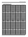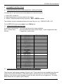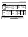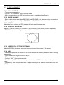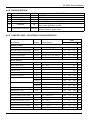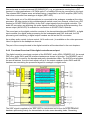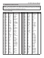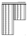
1
P/N:TCP520VEF0
Service Manual
COLOR Television
CHASSIS : CP-520V
Model : DTX-21G2/21B4/21U7
Caution
: In this Manual, some parts can be changed for improving. their
performance without notice in the parts list. So, if you need the
latest parts information, please refer to PPL(Parts Price List)in
Service Information Center.
Dec. 2006
CP-520V Service Manual
CONTENTS
DOCUMENT HISTORY
1 MAIN FEATURES
1.1 SPECIFICATIONS
1.1.1 GENERAL
1.1.2 EURO-SCART 1 (21 Pin)
1.1.3 EURO-SCART 2 (21 Pin)
1.2 CHANNEL/FREQUENCY TABLE
2 SAFETY INSTRUCTION
3 ALIGNMENT INSTRUCTIONS
3.1 MICROCONTROLLER CONFIGURATION : SERVICE MODE
3.2 SERVICE MODE NAVIGATION
3.3 MICROCONTROLLER CONFIGURATION : OPTION BITS
3.4 OPTION 1
3.5 OPTION 2
3.6 NVM DEFAULT SETTING
3.7 TV SET ALIGNMENT
3.7.1 G2 ALIGNMENT
3.7.2 WHITE BALANCE
3.7.3 FOCUS
3.7.4 VERTICAL GEOMETRY
3.7.5 HORIZONTAL PICTURE CENTRING
3.7.6 AGC
4 IC DESCRIPTION
4.1 UOC III SERIES
4.1.1 IC MARKING AND VERSION
4.1.2 BLOCK DIAGRAM
4.1.3 PINNING
4.1.4 FEATURES
4.2 LA42032 STEREO AUDIO AMPLI FIER
4.2.1 FEATURES
4.3 LA78040 VERTICAL AMPLIFIER
4.3.1 FEATURES
4.4 24WC16 - 16 KB EEPROM
4.5 STR - W6754
4.5.1 GENERAL DESCRIPTION
4.5.2 FEATURES
4.5.3 BLOCK DIAGRAM
4.5.4 PIN DESCRIPTION
4.5.5 CONTROL PART - ELECTRICAL CHARACTERISTICS
3
4
4
4
4
5
6
9
10
10
10
10
11
11
12
14
14
14
14
14
14
14
15
15
15
16
17
20
23
24
26
26
28
29
29
29
29
30
30
1
CP-520V Service Manual
5 CIRCUIT DESCRIPTION
5.1 BLOCK DIAGRAM
5.2 FUNCTIONAL DESCRIPTION OF VIDEO PROCESSOR
5.2.1 Vision IF amplifier
5.2.2 QSS sound circuit
5.2.3 FM demodulator
5.2.4 Audio input selector and volume contro
5.2.4.1 STEREO AND AV STEREO VERSIONS
5.2.4.2 MONO VERSIONS
5.2.5 CVBS and Y/C input signal selection
5.2.5.1 ALL VERSIONS
5.2.6 Synchronisation circuit
5.2.7 Horizontal and vertical drive
5.2.8 Chroma, luminance and feature processing
5.2.9 Colour decoder
5.2.10 RGB output circuit
5.2.11 I2C-BUS USER INTERFACE DESCRIPTION
5.3 GENERAL DESCRIPTION OF THE TV SOUND OF SOUND PROCESSOR
5.3.1 Supported standards
5.4 FUNCTIONAL DESCRIPTION SOUND PROCESSOR
5.4.1 The UOC III TV Sound Concept
5.4.2 Functional Overview Of the digital controller sound part
5.4.3 Demodulator and decoder
6 SERVICE PARTS LIST
6.1 DTX-21G2FZP-SB
7 EXPLODED VIEW
7.1 DTX-21G2
7.2 DTX-21B4
7.3 DTX-21U7
8 PRINTED CIRCUIT BOARD
8.1 4859813693(OLD PCB)
8.2 4859816393(NEW PCB)
9 SCHEMATIC DIAGRAM
9.1 CP-520V
32
32
33
33
33
33
34
34
34
34
34
35
36
36
37
38
40
40
41
42
42
43
44
47
47
52
52
53
54
55
55
56
57
57
2
CP-520V Service Manual
DOCUMENT HISTORY
VERSION
DATE
COMMENTS
V1.46
07/07/06 Creation of document (Author JS KIM) for project CP520 50Hz TV.
3
CP-520V Service Manual
1
MAIN FEATURES
1.1
SPECIFICATIONS
1.1.1 GENERAL
TV standard
Colour system
Sound system
Power
consumption
PAL - SECAM B/G D/K, PAL I/I, SECAM L/L’
Tuner PAL, SECAM
AV
PAL, SECAM, PAL 60, NTSC M, NTSC 4.43
NICAM B/G, I, D/K, L,
FM 2Carrier B/G, D/K
59W
Sound Output
Power
Speaker
4.5W x 2 (at 60% mod, 10% THD)
Teletext system
Aerial input
Channel coverage
Tuning system
Visual screen size
10 pages memory FASTEXT (FLOF or TOP)
75 ohm unbalanced
Off-air channels, S-cable channels and hyperband
frequency synthesiser tuning system
51cm
Channel indication
Program Selection
Aux. terminal
On Screen Display
100 programmes
EURO-SCART 1 : Audio / Video In and Out, R/G/B
In, Slow and Fast switching.
EURO-SCART 2 : Audio / Video In and Out, SVHS
In.
AV3 : Audio-Video Jack on front of cabinet.
Headphone jack (3.5 mm) on front of cabinet
SVHS3 (option) : Jack on front of cabinet – sound
input common with AV3.
R-49C10
12W 8 ohm x2
Remote Control
Unit
1.1.2 EURO-SCART 1 (21 Pin)
Pin
1
2
3
4
5
6
7
Signal Description
Audio Output Right
Audio Input Right
Audio Output Left
Audio Earth
Blue Earth
Audio Input Left
Blue Input
Matching value
0.5 Vrms, Impedance < 1 kΩ, ( RF 54% Mod )
0.5 Vrms, Impedance > 10 kΩ
0.5 Vrms, Impedance < 1 kΩ, ( RF 54% Mod )
0.5 Vrms, Impedance > 10 kΩ
0.7 Vpp ±0.1V, Impedance 75Ω
4
CP-520V Service Manual
8
Slow Switching
9
10
11
12
13
14
15
16
17
18
19
20
21
Green Earth
N.C.
Green Input
N.C.
Red Earth
Blanking Earth
Red Input
Fast Switching
Video Out Earth
Video In Earth
Video Output
Video Input
Common Earth
TV : 0 to 2V, AV 16/9 : 4.5 to 7V, AV 4/3 : 9.5 to 12V , Impedance
> 10 kΩ
0.7 Vpp ± 0.1V, Impedance 75Ω
0.7 Vpp ± 0.1V, Impedance 75Ω
0 to 0.4V : Logic “0”, 1 to 3V : Logic “1”, Impedance 75Ω
1 Vpp ± 3dB, Impedance 75Ω
1 Vpp ± 3dB, Impedance 75Ω
1.1.3 EURO-SCART 2 (21 Pin)
Pin
1
2
3
4
5
6
7
8
9
10
11
12
13
14
15
16
17
18
19
20
21
Signal Description
Audio Output Right
Audio Input Right
Audio Output Left
Audio Earth
Earth
Audio Input Left
N.C.
N.C.
N.C.
N.C.
N.C.
N.C.
Earth
Earth
Chroma Input
N.C.
Earth
Video In Earth
Video Output
Video Input, Y In.
Common Earth
Matching value
0.5 Vrms, Impedance < 1 kΩ, ( RF 54% Mod )
0.5 Vrms, Impedance > 10 kΩ
0.5 Vrms, Impedance < 1 kΩ, ( RF 54% Mod )
0.5 Vrms, Impedance > 10 kΩ
± 3dB for a luminance signal of 1 Vpp
1 Vpp ± 3dB, Impedance 75Ω ( Monitor output )
1 Vpp ± 3dB, Impedance 75Ω
5
CP-520V Service Manual
1.2
CHANNEL/FREQUENCY TABLE
CHANNEL
C01
C02
C03
C04
C05
C06
C07
C08
C09
C10
C11
C12
C13
C14
C15
C16
C17
C18
C19
C20
C21
C22
C23
C24
C25
C26
C27
C28
C29
C30
C31
C32
C33
C34
C35
C36
C37
C38
C39
C40
C41
C42
C43
C44
C45
EUROPE CCIR
46.25
48.25
55.25
62.25
175.25
182.25
189.25
196.25
203.25
210.25
217.25
224.25
53.75
82.25
183.75
192.25
201.25
471.25
479.25
487.25
495.25
503.25
511.25
519.25
527.25
535.25
543.25
551.25
559.25
567.25
575.25
583.25
591.25
599.25
607.25
615.25
623.25
631.25
639.25
647.25
655.25
663.25
FRANCE
55.75 (L')
60.5 (L')
63.75 (L')
176.00
184.00
192.00
200.00
208.00
216.00
189.25 (LUX)
69.25 (L')
76.25 (L')
83.25 (L')
90.25
97.25
471.25
479.25
487.25
495.25
503.25
511.25
519.25
527.25
535.25
543.25
551.25
559.25
567.25
575.25
583.25
591.25
599.25
607.25
615.25
623.25
631.25
639.25
647.25
655.25
663.25
GB(IRELAND)
45.75
53.75
61.75
175.25
183.25
191.25
199.25
207.25
215.25
223.25
231.25
239.25
247.25
49.75
57.75
65.75
77.75
85.75
471.25
479.25
487.25
495.25
503.25
511.25
519.25
527.25
535.25
543.25
551.25
559.25
567.25
575.25
583.25
591.25
599.25
607.25
615.25
623.25
631.25
639.25
647.25
655.25
663.25
EAST OIRT
49.75
59.25
77.25
85.25
93.25
175.25
183.25
191.25
199.25
207.25
215.25
223.25
471.25
479.25
487.25
495.25
503.25
511.25
519.25
527.25
535.25
543.25
551.25
559.25
567.25
575.25
583.25
591.25
599.25
607.25
615.25
623.25
631.25
639.25
647.25
655.25
663.25
6
CP-520V Service Manual
C46
C47
C48
C49
C50
C51
C52
C53
C54
C55
C56
C57
C58
C59
C60
C61
C62
C63
C64
C65
C66
C67
C68
C69
C70
C71
C72
C73
C74
C75
C76
C77
S01
S02
S03
S04
S05
S06
S07
S08
S09
S10
S11
S12
S13
S14
S15
S16
S17
671.25
679.25
687.25
695.25
703.25
711.25
719.25
727.25
735.25
743.25
751.25
759.25
767.25
775.25
783.25
791.25
799.25
807.25
815.25
823.25
831.25
839.25
847.25
855.25
863.25
69.25
76.25
83.25
90.25
97.25
59.25
93.25
105.25
112.25
119.25
126.25
133.25
140.25
147.25
154.25
161.25
168.25
231.25
238.25
245.25
252.25
259.25
266.25
273.25
671.25
679.25
687.25
695.25
703.25
711.25
719.25
727.25
735.25
743.25
751.25
759.25
767.25
775.25
783.25
791.25
799.25
807.25
815.25
823.25
831.25
839.25
847.25
855.25
863.25
104.75
116.75
128.75
140.75
152.75
164.75
176.75
188.75
200.75
212.75
224.75
236.75
248.75
260.75
272.75
284.75
296.75
671.25
679.25
687.25
695.25
703.25
711.25
719.25
727.25
735.25
743.25
751.25
759.25
767.25
775.25
783.25
791.25
799.25
807.25
815.25
823.25
831.25
839.25
847.25
855.25
863.25
103.25
111.25
119.25
127.25
135.25
143.25
151.25
159.25
167.25
255.25
263.25
271.25
279.25
287.25
671.25
679.25
687.25
695.25
703.25
711.25
719.25
727.25
735.25
743.25
751.25
759.25
767.25
775.25
783.25
791.25
799.25
807.25
815.25
823.25
831.25
839.25
847.25
855.25
863.25
105.25
112.25
119.25
126.25
133.25
140.25
147.25
154.25
161.25
168.25
231.25
238.25
245.25
252.25
259.25
266.25
273.25
7
CP-520V Service Manual
S18
S19
S20
S21
S22
S23
S24
S25
S26
S27
S28
S29
S30
S31
S32
S33
S34
S35
S36
S37
S38
S39
S40
S41
280.25
287.25
294.25
303.25
311.25
319.25
327.25
335.25
343.25
351.25
359.25
367.25
375.25
383.25
391.25
399.25
407.25
415.25
423.25
431.25
439.25
447.25
455.25
463.25
136.00
160.00
303.25
311.25
319.25
327.25
335.25
343.25
351.25
359.25
367.25
375.25
383.25
391.25
399.25
407.25
415.25
423.25
431.25
439.25
447.25
455.25
463.25
295.25
303.25
311.25
319.25
327.25
335.25
343.25
351.25
359.25
367.25
375.25
383.25
391.25
399.25
407.25
415.25
423.25
431.25
439.25
447.25
455.25
463.25
280.25
287.25
294.25
303.25
311.25
319.25
327.25
335.25
343.25
351.25
359.25
367.25
375.25
383.25
391.25
399.25
407.25
415.25
423.25
431.25
439.25
447.25
455.25
463.25
8
CP-520V Service Manual
2
SAFETY INSTRUCTION
WARNING: Only competent service personnel may carry out work involving the testing or repair
of this equipment.
X-RAY RADIATION PRECAUTION
1.
Excessive high voltage can produce potentially hazardous X-RAY RADIATION. To avoid
such hazards, the high voltage must not exceed the specified limit. The nominal value of the high
voltage of this receiver is 25KV at max beam current.
The high voltage must not, under any circumstances, exceed 29KV.
Each time a receiver requires servicing, the high voltage should be checked. It is important to
use an accurate and reliable high voltage meter.
2.
The only source of X-RAY Radiation in this TV receiver is the picture tube. For continued
X-RAY RADIATION protection, the replacement tube must be exactly the same type tube as
specified in the parts list.
SAFETY PRECAUTION
Potentials of high voltage are present when this receiver is operating. Operation of the receiver
outside the cabinet or with the back board removed involves a shock hazard from the receiver.
Servicing should not be attempted by anyone who is not thoroughly familiar with the precautions
necessary when working on high voltage equipment.
Discharge the high potential of the picture tube before handling the tube. The picture tube is
highly evacuated and if broken, glass fragments will be violently expelled.
If any Fuse in this TV receiver is blown, replace it with the FUSE specified in the Replacement
Parts List.
When replacing a high wattage resistor (metal oxide film resistor) in the circuit board, keep the
resistor 10 mm away from circuit board.
Keep wires away from high voltage or high temperature components.
This receiver must operate under AC 230 volts, 50 Hz. NEVER connect to a DC supply or any
other voltage or frequency.
PRODUCT SAFETY NOTICE
Many electrical and mechanical parts in this equipment have special safety-related
characteristics. These characteristics are often passed unnoticed by a visual inspection and the
X-RAY RADIATION protection afforded by them cannot necessarily be obtained by using
replacement components rated for higher voltage, wattage, etc. Replacement parts which have
these special safety characteristics are identified in this manual and its supplements, electrical
components having such features are identified by designated symbol on the parts list. Before
replacing any of these components, read the parts list in this manual carefully. The use of
substitutes replacement parts which do not have the same safety characteristics as specified in
the parts list may create X-RAY Radiation.
9
CP-520V Service Manual
3
3.1
ALIGNMENT INSTRUCTIONS
MICROCONTROLLER CONFIGURATION : SERVICE MODE
To switch the TV set into service mode please see instruction below.
1 - Select PR. number 91
2 - Adjust sharpness to minimum and exit all menus.
3 – Within 2 seconds press the key sequence : RED - GREEN - menu
The software version is displayed beside the word Service, e.g. “SERVICE VER 1.46”.
To exit SERVICE menu press menu key or Std By key.
3.2
SERVICE MODE NAVIGATION
Pr Up/Down remote keys : cycle through the service items available.
Vol -/+ remote keys
: Dec./Increment the values within range – Cycle trough option bits.
OK key
: Toggle bits in option byte
Order
1
2
3
4
5
6
7
8
9
10
11
12
13
14
15
16
17
18
19
20
21
22
3.3
Item
HOR CEN
RED GAIN
GRN GAIN
BLUE GAIN
RED BIAS
GRN BIAS
AGC LEVEL
G2 – SCREEN
OPTION1
OPTION2
AVL
PARABOLA
HOR WIDTH
CORNER T
CORNER B
HOR. PARAL
V. LINEAR
V. SLOPE
EW TRAPEZ
S CORRECT
VERT CENT
VERT SIZE
Default setting
MICROCONTROLLER CONFIGURATION : OPTION BITS
There are two option bytes available (16 bits in all). These option bits are available from Service
mode. First find the OPTION1 or OPTION2 control, and then use the Volume PLUS/MINUS
buttons on the remote control keypad to locate the bits, and OK key to toggle them. The table
below shows the two option bytes available;
10
CP-520V Service Manual
3.4
OPTION 1
B7
TOP
1 Teletext
OFF
TOP
0 Teletext
ON
3.5
FASTEXT
(FLOF) ON
B5
TUBE
4:3
TUBE
16:9
OPTION 2
B7
1
0
B6
FASTEXT
(FLOF)
OFF
Fixed to
‘ 0’
B6
JVC
remote
control
B5
AVL
control
OFF
Daewoo
Remote
control
AVL
control
ON
OPTION
CHASSIS
MODEL
CP-520V
DTX-21G2/B4/U7
I
II
B4
VAI bit set
to 1 in
SECAM L
VAI bit set
to 0 in
SECAM L
B3
Dolby
Virtual
OFF
Dolby
Virtual
ON
B4
B3
5 keys
local
keyboard
PICTURE
TILT ON
PICTURE
TILT OFF
OPTION
BIT[b7…b0]
0011
1110
0000
1111
7 keys
lacal
keyboard
B2
B1
SVHS3
disable
SVHS3
enable
B2
Full
ATSS
Basic
ATSS
B0
TUNER OPTIONS
00 = Philips
01 = Not used
10 = Alps, LG
11 = Parstnic, SS
B1
Double
Window
Enabled
Double
Window
Disabled
DW[hex]
REMARKS
3E
0F
OPTION1 “ b1,b0” depends on Tuner
B0
n.u.
Must
be set
to 1 for
future
compa
tibility
11
CP-520V Service Manual
3.6
NVM default setting
The purpose of this message, when you change a virgin EEPROM, is to allow to modify
the NVM DATA to desired values.
1 - Introduction :
The NVM default valus are fixed for the user, but for flexibility in service, these data are stored in
NVM and can be changed when the TV set is in a special mode call "NVM EDITOR". This mode
can only be access from "FACTORY" mode.
2 - Entering into "FACTORY" mode.
To switch the TV set into FACTORY mode, use the factory remote control, and press on “SVC”
key. The factory menu will appear on the screen, showing “FACTORY” , plus other relevant
information like software version and date.
WARNING : When in "FACTORY" mode you should not press any key other than the keys
described in the procedure below. Unwanted key stroke could misadjust the TV set.
3 - Entering into "NVM EDITOR" mode.
To switch the TV set into NVM EDITOR mode, use the user remote control, and press on
“PICTURE/OK” key. The NVM EDITOR window will appear on the screen. This mode allow you
to access all data stored in NVM. The current NVM address is given in column "ADDR." in both
DECimal and HEXadecimal format. The column DATA gives the value contained at selected
address in both DECimal and HEXadecimal format.
4 - Navigation in "NVM EDITOR" mode.
Use Program Up/Dwn keys to select the desired address. Use Volume Up/Dwn keys to change
the data at selected address. You must press "PICTURE/OK" key to store value after
modification.
The data can be adjusted between 0 and 63.
5 - Exit "NVM EDITOR" mode.
To switch the TV set back into FACTORY mode, use the user remote control, and press on
“MENU” key.
The factory menu will appear on the screen, showing “FACTORY”.
6 - Exit "FACTORY" mode.
To exit "FACTORY" mode, use the factory remote control, and press on “SVC” key.
The factory menu will disappear from the screen.
12
CP-520V Service Manual
NVM DATA CHANGE LIST
No
Register Name
Address
(hex)
Default
CP-520V
21G2/B4/U7
1
OCP_THRESHOLD
0x58F
0x91
<-
2
DCXO
0x590
0x4E
<-
3
AGC_PHILIPS
0x5C1
0xAB
<-
4
AGC_NC
0x5C2
0xAB
<-
5
AGC_ALPS, LG
0x5C3
0xB6
<-
6
AGC_PARTSNIC
0x5C4
0xB6
<-
7
AGC_PHILIPS_START
0x5C5
0x16
8
AGC_NC_START
0x5C6
0x16
O x OF
O x OF
9
AGC_ALPS, LG_START
0x5C7
0x16
O x OF
10
AGC_PARTSNIC_START
0x5C8
0x16
O x OF
11
AVLLEV
0x621
0x5
<-
12
Nor1_Bright
0x64A
0x23
<-
13
Nor1_contrast
0x64B
0x2E
<-
14
Nor1_Colour
0x64C
0x1C
<-
15
Nor1_Sharpness
0x64D
0x23
<-
16
Nor1_Tint
0x64E
0x20
<-
17
Nor1_JVC_Bri
0x64F
0x2D
<-
18
Nor1_JVC_Cont
0x650
0x2A
<-
19
Nor1_JVC_Colour
0x651
0x1B
<-
20
Nor1_JVC_Sharp
0x652
0x23
<-
21
Nor2_Bright
0x653
0x28
<-
22
Nor2_Contrast
0x654
0x13
<-
23
Nor2_Colour
0x655
0x19
<-
24
Nor2_Sharpness
0x656
0x1B
<-
25
Nor2_Tint
0x657
0x20
26
PresetGainRGB
0x673
0x2A
<O x 10
27
PresetGainRGB
0x674
0x2A
O x 10
28
PresetGainRGB
0x675
0x2A
O x 10
29
Cathode_Drive
0x67B
0x1
30
Y_delay_PAL_BG
0x686
0x5
<O x 02
31
Y_delay_SECAM_BG
0x687
0x8
O x 0B
32
Y_delay_PAL_DK
0x688
0x5
Ox0
33
Y_delay_SCM_DK
0x689
0x5
O x 08
34
Y_delay_PAL_I
0x68A
0x7
O x 0B
35
Y_delay_SECAM
0x68B
0x5
O x 07
36
Y_delay_SECAM-L
0x68C
0x8
O x 07
37
Y_delay_AV
0x68D
0xA
O x 05
38
G2_Bright
0x68E
0x1A
0x28
39
G2_Contrast
0x68F
0x42
<-
13
CP-520V Service Manual
3.7
TV SET ALIGNMENT
3.7.1 G2 ALIGNMENT
- Tune a colour bar pattern.
- Find the “G2 – SCREEN” item in service mode.
- Adjust screen volume (on FBT) to bring the cursor to central position(Green).
3.7.2 WHITE BALANCE
- Select a dark picture and adjust RED BIAS and GRN BIAS to the desired colour temperature.
- Select a bright picture and adjust RED, GRN and BLUE GAIN to the desired colour temperature.
3.7.3 FOCUS
Adjust the Focus volume (on FBT) to have the best resolution on screen.
3.7.4 VERTICAL GEOMETRY
Adjust V. LINEAR (linearity), S CORRECT (S. Correction), VERT SIZE (Vertical amplitude),
VERT CENT (vertical centring) to compensate for vertical distortion.
3.7.5 HORIZONTAL PICTURE CENTRING
Adjust HOR CEN (Horizontal centre) to have the picture in the centre of the screen.
3.7.6 AGC
- Make sure option bits are correct for the tuner fitted on the chassis (See above how to change
option bits).
- Adjust the antenna signal level at 62 dBµV
- Tune a colour bar pattern.
- Find the “AGC” item in service mode.
- Press the key “OK” on the remote keypad and wait until AGC level stabilise to the optimum
value.
- Alternatively, use “Vol Up/Dwn” keys to adjust manually to the desired Tuner Take Over Point
(TOP).
14
CP-520V Service Manual
4
IC DESCRIPTION
4.1
UOC III Series
The UOCIII series combines the functions of a Video Signal Processor (VSP) together with a
FLASH embedded TEXT/Control/Graphics µ-Controller (TCG µ-Controller) and US Closed
Caption decoder. In addition the following functions can be added:
• Adaptive digital (4H/2H) PAL/NTSC combfilter
• Teletext decoder with 10 page text memory
• Multi-standard stereo decoder
• BTSC stereo decoder
• Digital sound processing circuit
• Digital video processing circuit
4.1.1 IC MARKING AND VERSION
Chassis
CP-520V
IC marking
OSD languages
ATSS countries
Text
BULGARIAN,
CZECH, GERMAN,
DANISH, SPANISH,
FRENCH, FINNISH,
ENGLISH, GREEK,
HUNGARIAN,
ITALIAN,
NORWEGIAN,
DUTCH, POLISH,
ROMANIAN,
RUSSIAN,
SWEDISH,
SLOVAKIAN.
Austria, Belgium,
Switzerland, Czech
Republic, Germany,
Denmark, Spain,
France, Finland, GB,
Greece, Hungary, Italy,
Ireland, Norway,
Netherlands, Portugal,
Poland, Sweden,
Slovak Republic,
Others
PAN-EUROPEAN
LATIN, CYRILLIC,
GREEK.
15
CP-520V Service Manual
4.1.2. BLOCK DIAGRAM
16
CP-520V Service Manual
4.1.3. PINNING
QFP 128pin
1
2
3
4
5
6
7
8
9
10
11
12
13
14
15
16
17
18
Symbol
P1.5/TX
P1.4/RX
P1.2/INT2
VSSC3
VDDC3
P2.5/PWM4
P2.4/PWM3
VSSC/P
P3.3/ADC3
P3.2/ADC2
DECV1V8
VDDC1
P3.1/ADC1
P3.0/ADC0
P2.3/PWM2
P2.2/PWM1
P2.1/PWM0
P2.0/TPWM
19
VDDP(3.3V)
20
21
22
23
24
25
26
27
28
29
30
31
P1.7/SDA
P1.6/SCL
P1.3/T1
P0.0/I2SDI1/O
P0.1/I2SDO1
P0.2/I2SDO2
P0.3/I2SCLK
P0.4/I2SWS
VSSC2
VDDC2
P1.1/T0
P1.0/INT1
32
INT0/P0.5
33
34
35
36
37
38
39
40
VDDadc(1.8)
VSSadc
VDDA2(3.3)
VDDA(1.8)
GNDA
VREFAD
VREFAD_POS
VREFAD_NEG
41
VDDA1
42
BO
Short Description
Port 1.5 or UART bus
port 1.4 or UART bus
port 1.2 or external interrupt 2
Ground
digital supply to core (1.8V)
port 2.5 or PWM4 output
port 2.4 or PWM3 output
digital ground for m-Controller core and periphery
port 3.3 or ADC3 input
port 3.2 or ADC2 input
decoupling 1.8 V supply
digital supply to core (+1.8 V)
port 3.1 or ADC1 input
port 3.0 or ADC0 input
port 2.3 or PWM2 output
port 2.2 or PWM1 output
port 2.1 or PWM0 output
port 2.0 or Tuning PWM output
supply to periphery and on-chip voltage regulator (3.3
V)
port 1.7 or I2C-bus data line
port 1.6 or I2C-bus clock line
port 1.3 or Counter/Timer 1 input
port 0.0 or I2S digital input 1 or I2S digital output
port 0.1 or I2S digital output 1
port 0.2 or I2S digital output 2
port 0.3 or I2S clock
port 0.4 or I2S word select
Ground
digital supply to core (1.8 V)
port 1.1 or Counter/Timer 0 input
port 1.0 or external interrupt 1
external interrupt 0 or port 0.5 (4 mA current sinking
capability for direct drive of LEDs)
supply voltage video ADC
ground for on-chip temperature sensor
supply voltage SDAC (3.3 V)
analogue supply for audio ADCs (1.8 V)
Ground
reference voltage for audio ADCs (3.3/2 V)
positive reference voltage (3.3 V)
negative reference voltage (0 V)
analog supply for TCG m-Controller and digital supply
for
TV-processor (+3.3 V)
Blue output
17
CP-520V Service Manual
43
44
45
46
47
48
49
50
51
52
53
54
55
56
57
58
59
60
61
62
63
64
65
66
67
68
69
70
71
72
73
74
75
76
77
78
79
80
81
82
83
84
85
86
GO
RO
BLKIN
BCLIN
VP3
GND3
B/PBIN3
G/YIN3
R/PRIN3
INSSW3
Green output
Red output
black current input
beam current limiter input
3rd supply for TV processor
ground 3 for TV-processor
3rd B input / PB input
3rd G input / Y input
3rd R input / PR input
3rd RGB / YPBPR insertion input
V-output for YUV interface (general purpose switch
VOUT(SWO1)
output)
U-output for YUV interface (2nd RGB / YPBPR
UOUT(INSSW2)
insertion input)
YOUT
Y-output (for YUV interface)
YSYNC
Y-input for sync separator
Y-input for YUV interface (2nd G input / Y input or
YIN (G/YIN2/CVBS-Yx)
CVBS/YX input))
UIN (B/PBIN2)
U-input for YUV interface (2nd B input / PB input)
V-input for YUV interface (2nd R input / PR input or CX
VIN (R/PRIN2/CX)
input)
VDDcomb
supply voltage for comb filter (5 V)
VSScomb
ground connection for comb filter
HOUT
horizontal output
flyback input/sandcastle output or composite H/V
FBISO/CSY
timing output
SVM
scan velocity modulation output
CVBSO/PIP
CVBS / PIP output
AUDOUTHPR
audio output for headphone channel (right signal)
AUDOUTHPL
audio output for headphone channel (left signal)
AUDOUTLSR
audio output for audio power amplifier (right signal)
AUDOUTLSL
audio output for audio power amplifier (left signal)
C2/C3
chroma-2/3 input
CVBS3/Y3
CVBS3/Y3 input
AUDIOIN3R
audio 3 input (right signal)
AUDIOIN3L
audio 3 input (left signal)
CVBS2/Y2
CVBS2/Y2 input
AUDIOIN2R
audio 2 input (right signal)
AUDIOIN2L
audio 2 input (left signal)
C4
chroma-4 input
CVBS4/Y4
CVBS4/Y4 input
AUDIOIN4R
audio-4 input (right signal)
AUDIOIN4L
audio-4 input (left signal)
IFVO/SVO/CVBSI (2) IF video output / selected CVBS output / CVBS input
VP2
2nd supply voltage TV processor (+5 V)
AGC2SIF
AGC capacitor second sound IF
VCC8V
8 Volt supply for audio switches
DVBO/FMRO (2)
Digital Video Broadcast output / FM radio output
Digital Video Broadcast output / IF video output / FM
DVBO/IFVO/FMRO (2)
radio output
18
CP-520V Service Manual
87
SIFAGC/DVBAGC (2)
88
89
PLLIF
GND2
90
QSSO/AMOUT/AUDEE
M (2)
91
92
93
94
95
DECSDEM
AUDOUTSR
AUDOUTSL
AUDIOIN5R
AUDIOIN5L
96
AVL/SWO/SSIF/
REFO/REFIN (2)
97
98
99
100
101
102
103
104
105
106
107
108
109
110
111
112
113
114
115
EHTO
AGCOUT
SIFIN2/DVBIN2 (2)
SIFIN1/DVBIN1 (2)
GNDIF
IREF
VSC
VIFIN2
VIFIN1
VDRA
VDRB
EWD/AVL (1)
DECBG
SECPLL
GND1
PH1LF
PH2LF
VP1
DECDIG
116
VGUARD/SWIO
117
118
119
120
121
122
123
124
125
126
127
128
VSSA1
XTALOUT
XTALIN
VREF_POS_HPR
VREF_NEG_HPL+HPR
VREF_POS_LSR+HPR
VREF_NEG_LSL+HPL
VREF_POS_LSL
VDDA3(3.3V)
VDDC4
VSSC4
VSSP2
AGC sound IF / internal-external AGC for DVB
applications
IF-PLL loop filter
ground 2 for TV processor
QSS intercarrier output / AM output / deemphasis
(front-end audio
out)
decoupling sound demodulator
audio output for SCART/CINCH (right signal)
audio output for SCART/CINCH (left signal)
audio-5 input (right signal)
audio-5 input (left signal)
Automatic Volume Levelling / switch output / sound IF
input /
subcarrier reference output / external reference signal
input for I
signal mixer for DVB operation
EHT/overvoltage protection input
tuner AGC output
SIF input 2 / DVB input 2
SIF input 1 / DVB input 1
ground connection for IF amplifier
reference current input
vertical sawtooth capacitor
IF input 2
IF input 1
vertical drive A output
vertical drive B output
East-West drive output or AVL capacitor
bandgap decoupling
SECAM PLL decoupling
ground 1 for TV-processor
phase-1 filter
phase-2 filter
1st supply voltage TV-processor (+5 V)
decoupling digital supply
V-guard input / I/O switch (e.g. 4 mA current sinking
capability for
direct drive of LEDs)
Ground
crystal oscillator output
crystal oscillator input
positive reference voltage SDAC (3.3 V)
negative reference voltage SDAC (0 V)
positive reference voltage SDAC (3.3 V)
negative reference voltage SDAC (0 V)
positive reference voltage SDAC (3.3 V)
supply (3.3 V)
digital supply to SDACs (1.8V)
Ground
Ground
19
CP-520V Service Manual
4.1.4 FEATURES
Analogue Video Processing (all versions)
· Multi-standard vision IF circuit with alignment-free PLL demodulator
· Internal (switchable) time-constant for the IF-AGC circuit
· Switchable group delay correction and sound trap (with switchable centre frequency) for the
demodulated CVBS signal
· DVB/VSB IF circuit for preprocessing of digital TV signals.
· Video switch with 3 external CVBS inputs and a CVBS output. All CVBS inputs can be used as
Y-input for Y/C signals. However, only 2 Y/C sources can be selected because the circuit has 2
chroma inputs. It is possible to add an additional CVBS(Y)/C input (CVBS/YX and CX) when the
YUV interface and the RGB/YPRPB input are not needed.
· Automatic Y/C signal detector
· Adaptive digital (4H/2H) PAL/NTSC comb filter for optimum separation of the luminance and the
chrominance signal.
· Integrated luminance delay line with adjustable delay time
· Picture improvement features with peaking (with switchable centre frequency, depeaking,
variable positive/negative peak ratio, variable pre-/overshoot ratio and video dependent coring),
dynamic skin tone control, gamma control and blue- and black stretching. All features are
available for CVBS, Y/C and RGB/YPBPR signals.
· Switchable DC transfer ratio for the luminance signal
· Only one reference (24.576 MHz) crystal required for the TCG m-Controller, digital sound
processor, Teletext and the colour decoder
· Multi-standard colour decoder with automatic search system and various “forced mode”
possibilities
· Internal base-band delay line
· Indication of the Signal-to-Noise ratio of the incoming CVBS signal
· Linear RGB/YPBPR input with fast insertion.
· YUV interface. When this feature is not required some pins can be used as additional
RGB/YPBPR input. It is also possible to use these pins for additional CVBS (or Y/C) input
(CVBS/YX and CX).
· Tint control for external RGB/YPBPR signals
· Scan Velocity Modulation output. The SVM circuit is active for all the incoming CVBS, Y/C and
RGB/YPBPR signals. The SVM function can also be used during the display of teletext pages.
· RGB control circuit with ‘Continuous Cathode Calibration’, white point and black level off-set
adjustment so that the colour temperature of the dark and the light parts of the screen can be
chosen independently.
· Contrast reduction possibility during mixed-mode of OSD and Text signals
· Adjustable ‘wide blanking’ of the RGB outputs
· Horizontal synchronization with two control loops and alignment-free horizontal oscillator
· Vertical count-down circuit
· Vertical driver optimized for DC-coupled vertical output stages
· Horizontal and vertical geometry processing with horizontal parallelogram and bow correction
and horizontal and vertical zoom
· Low-power start-up of the horizontal drive circuit
Analogue video processing (stereo versions)
· The low-pass filtered ‘mixed down’ I signal is available via a single ended or balanced output
stage.
Analogue video processing (mono versions)
· The low-pass filtered ‘mixed down’ I signal is available via a single ended output stage
Digital Video Processing (some versions)
· Double Window mode applications. It is possible to display a video and a text window or 2 text
20
CP-520V Service Manual
windows in parallel.
· Linear and non-linear horizontal scaling of the video signal to be displayed.
Sound Demodulation (all versions)
· Separate SIF (Sound IF) input for single reference QSS (Quasi Split Sound) demodulation.
· AM demodulator without extra reference circuit
· The mono intercarrier sound circuit has a selective FM-PLL demodulator which can be switched
to the different FM sound frequencies (4.5/5.5/6.0/6.5 MHz). The quality of this system is such
that the external band-pass filters can be omitted. In the stereo versions of UOCIII the use of this
demodulator is optional for special applications. Normally the FM demodulators of the stereo
demodulator/decoder part are used (see below).
· The FM-PLL demodulator can be set to centre frequencies of 4.72/5.74 MHz so that a second
sound channel can be demodulated. In such an application it is necessary that an external
bandpass filter is inserted.
· The vision IF and mono intercarrier sound circuit can be used for the demodulation of FM radio
signals. With an external FM tuner also signals with an IF frequency of 10.7 MHz can be
demodulated.
· Switch to select between 2nd SIF from QSS demodulation or external FM (SSIF)
Audio Interfaces and switching (stereo versions with Audio DSP)
· Audio switch circuit with 4 stereo inputs, a stereo output for SCART/CINCH, 1 stereo output for
HEADPHONE. The headphone channel has an analogue volume control circuit for the L and R
channel. Finally 1 stereo SPEAKER output with digital controls.
· AVL (Automatic Volume Levelling) circuit for the headphone channel.
· Digital input crossbar switch for all digital signal sources and destinations
· Digital output crossbar for exchange of channel processing functionality
· Digital audio input interface (stereo I2S input interface)
· Digital audio output interface (stereo I2S output interface)
Audio interfaces and switching (AV stereo versions without Audio DSP)
· Audio switch circuit with 4 stereo inputs, a stereo output for SCART/CINCH and a stereo
SPEAKER output with analogue volume control.
· Analogue mono AVL circuit at left audio channel
Audio interfaces and switching (mono versions)
· Audio switch circuit with 4 external audio (mono) inputs and a volume controlled output
· AVL circuit
Stereo Demodulator and Decoder (full stereo versions)
· Demodulator and Decoder Easy Programming (DDEP)
· Auto standard detection (ASD)
· Static Standard Selection (SSS)
· DQPSK demodulation for different standards, simultaneously with 1-channel FM demodulation
· NICAM decoding (B/G, I, D/K and L standard)
· Two-carrier multistandard FM demodulation (B/G, D/K and M standard)
· Decoding for three analog multi-channel systems (A2, A2+ and A2*) and satellite sound
· Adaptive de-emphasis for satellite FM
· Optional AM demodulation for system L, simultaneously with NICAM
· Identification A2 systems (B/G, D/K and M standard) with different identification time constants
· FM pilot carrier present detector
· Monitor selection for FM/AM DC values and signals, with peak and quasi peak detection option
· BTSC MPX decoder
· SAP decoder
· dbx® noise reduction (4)
· Japan (EIAJ) decoder
· FM radio decoder
· Soft-mute for DEMDEC outputs DEC, MONO and SAP
21
CP-520V Service Manual
· FM overmodulation adaptation option to avoid clipping and distortion
Audio Multi Channel Decoder (stereo versions with Audio DSP)
· Dolby® Pro Logic® (DPL) (1)
· Five channel processing for Main Left and Right, Subwoofer, Centre and Surround. To exploit
this feature an external DAC is required.
Volume and tone control for loudspeakers (stereo versions with Audio DSP)
· Automatic Volume Level (AVL) control
· Smooth volume control
· Master volume control
· Soft-mute
· Loudness
· Bass, Treble
· Dynamic Bass Boost (DBB) (2)
· Dynamic Virtual Bass (DVB) (3)
· BBE® Sound processing (4)
· Graphic equalizer
· Processed or non processed subwoofer
· Programmable beeper
Reflection and delay for loudspeaker channels (stereo versions with Audio DSP)
· Dolby® Pro Logic® Delay (1)
· Pseudo hall/matrix function
Psycho acoustic spatial algorithms, downmix and split in loudspeaker channels (stereo
versions with Audio DSP)
· Extended Pseudo Stereo (EPS) (5)
· Extended Spatial Stereo (ESS) (6)
· Virtual Dolby® Surround (VDS 422,423) (1)
· SRS 3D and SRS TruSurround® (4)
RDS/RBDS
· Demodulation of the European Radio Data system (RDS) or the USA Radio Broadcast Data
System (RBDS) signal
· RDS and RBDS block detection
· Error detection and correction
· Fast block synchronisation
· Synchronisation control (flywheel)
· Mode control for RDS/RBDS processing
· Different RDS/RBDS block information output modes
m-Controller
· 80C51 m-controller core standard instruction set and timing
· 0.4883 ms machine cycle
· maximum of 256k x 8-bit flash programmable ROM
· maximum of 8k x 8-bit Auxiliary RAM
· 12-level Interrupt controller for individual enable/disable with two level priority
· Two 16-bit Timer/Counter registers
· One 24-bit Timer (16-bit timer with 8-bit Pre-scaler)
· WatchDog timer
· Auxiliary RAM page pointer
· 16-bit Data pointer
· Stand-by, Idle and Power Down modes
· 24 general I/O
· 14 bits PWM for Voltage Synthesis Tuning
· 8-bit A/D converter with 4 multiplexed inputs
22
CP-520V Service Manual
· 5 PWM (6-bits) outputs for analogue control functions
· Remote Control Pre-processor (RCP)
· Universal Asynchronous Receiver Transmitter (UART)
Data Capture
· Text memory up to 10 pages
· Inventory of transmitted Teletext pages stored in the Transmitted Page Table (TPT) and Subtitle
Page Table (SPT)
· Data Capture for US Closed Caption
· Data Capture for 525/625 line WST, VPS (PDC system A) and Wide Screen Signalling (WSS)
bit decoding
· Automatic selection between 525 WST/625 WST
· Automatic selection between 625 WST/VPS on line 16 of VBI
· Real-time capture and decoding for WST Teletext in Hardware, to enable optimized mprocessor throughput
· Automatic detection of FASTEXT transmission
· Real-time packet 26 engine in Hardware for processing accented, G2 and G3 characters
· Signal quality detector for video and WST/VPS data types
· Comprehensive teletext language coverage
· Vertical Blanking Interval (VBI) data capture of WST data
Display
· Teletext and Enhanced OSD modes
· Features of level 1.5 WST and US Close Caption
· 50Hz/60Hz display timing modes
· Two page operation for 16:9 screens
· Serial and Parallel Display Attributes
· Single/Double/Quadruple Width and Height for characters
· Smoothing capability of both Double Size, Double Width & Double Height characters
· Scrolling of display region
· Variable flash rate controlled by software
· Soft colours using CLUT with 4096 colour palette
· Globally selectable scan lines per row (9/10/13/16/) and character matrix [12x9, 12x10, 12x13,
12x16, 16x18, (VxH)]
· Fringing (Shadow) selectable from N-S-E-W direction
· Fringe colour selectable
· Contrast reduction of defined area
· Cursor
· Special Graphics Characters with two planes, allowing four colours per character
· 64 software redefinable On-Screen display characters
· 4 WST Character sets (G0/G2) in single device (e.g. Latin, Cyrillic, Greek, Arabic)
· G1 Mosaic graphics, Limited G3 Line drawing characters
· WST Character sets and Closed Caption Character set in single device
· SVM for Text
4.2
LA42032 STEREO AUDIO AMPLIFIER
The LA42032 is a dual-channel audio power amplifier with an output power of 2 x 5 W at an 8
Ω load and a 9 V supply.
23
CP-520V Service Manual
4.2.1 FEATURES
•
•
•
•
5W x 2 Channel(Vcc=9V, RL=8Ω)
Standby function
Mute function
Thermal protection circuit
Pin description
Pin
1
2
3
4
5
6
7
8
9
10
11
12
13
Symbol
R.F.
Rin
GND
Lin
STB
Mute
Vcc
Lo(+)
Lo(-)
GND
Ro(-)
Ro(+)
N.C.
Description
Ripple Filter
Right input
Ground
Left Input
Standby
Mute
Supply Voltage
Positive Left output
Negative Left Output
Ground
Negative Right Output
Positive Right Output
Not Connected
R.F.
1
Rin
2
GND
3
Lin
4
STB
5
Mute
6
Vcc
7
Lo(+)
8
Lo(-)
9
LA42032
GND 10
Ro(-) 11
Ro(+) 12
N.C. 13
MBK932
24
CP-520V Service Manual
Block diagram LA42032
25
CP-520V Service Manual
4.3
LA78040 VERTICAL AMPLIFIER
The LA78040 are power circuit for use in 90° and 110° colour deflection systems for field
frequencies of 25 to 200Hz field frequencies, and for 4:3 and 16/9 picture tubes. The IC contains
a vertical deflection output circuit, operating as a high efficiency class G system. The full bridge
output circuit allows DC coupling of the deflection coil in combination with single positive supply
voltages.
4.3.1 FEATURES
§
§
§
Built-in pump-up circuti for low power dissipation
Vertical output circuit
Thermal protection circuit
Vin(-)
1
Vcc
2
Pump Up Out
3
-14V
4
Vout
5
Vcc
6
Vin(+)
7
LA78040
MGL867
26
CP-520V Service Manual
Pinning
Pin
1
2
3
4
5
6
7
Symbol
Vin(-)
Vcc
Pump Up Out
-14V
Vout
Vcc
Vin(+)
Description
Inverting Input
Supply voltage
Pump Up Out
-14V
Ver. Output
Output Stage Vcc
Non Inv. Input
Block diagram LA78040
27
CP-520V Service Manual
4.4
24WC16 - 16 KB EEPROM
Features :
§ 16 Kbit serial I2C bus EEPROM
§ 400KHz I2C Bus Compatible
§ supply voltage : 1.8 V to 6.0 V
§ Low Power CMOS Technology
§ 1 Million Erase/Write cycles (minimum)
§ 100 year data retention (minimum)
Pin description
Pin No.
Name
1, 2, 3 A0, A1, A2
5
SDA
6
SCL
7
WP
8
Vcc
4
Vss
Description
Device address – not used
Serial Data/Address Input/Output
Serial clock
Write control
Supply voltage
Ground
The memory device is compatible with the I2C memory standard. This is a two wire serial
interface that uses a bi-directional data bus and serial clock. The memory carries a built-in 4-bit
unique device type identifier code (1010) in accordance with the I2C bus definition.
Serial Clock (SCL)
The SCL input is used to strobe all data in and out of the memory.
Serial Data (SDA)
The SDA pin is bi-directional, and is used to transfer data in or out of the memory.
28
CP-520V Service Manual
4.5
STR - W6754
4.5.1 GENERAL DESCRIPTION
The STR-W6754 is a quasi-resonant regulator specifically designed
to satisfy the requirements for increased integration and reliability in
switch-mode power supplies. It incorporates a primary control and drive
circuit with an avalanche-rated power MOSFET.
4.5.2 FEATURES
• Auto-Bias Function Stable Burst Operation Without Generating Interference
• Internal Off-Timer Circuit
• Built-In Constant-Voltage Drive
• Multiple Protections: Pulse-by-Pulse Overcurrent Protection
Overload Protection with Auto Recovery
Latching Overvoltage Protection
Undervoltage Lockout with Hysteresis
• RoHS Compliant
4.5.3 BLOCK DIAGRAM
29
CP-520V Service Manual
4.5.4 PIN DESCRIPTION
PIN
1
3
4
5
NAME
Drain
Source/Ground
Supply
Overload Protection
6
Feedback
7
Overcurrent Protection
SYMBOL
D
S/GND
Vcc
SS/OLP
DESCRIPTION
MOSFET drain
Ground
Power Supply
Overload Protection and Soft Start Operation Time set up
Constant Voltage Control Signal Input,
FB
Burst mode Oscillation Control
Overcurrent Protection Signal Input/
OCP/BD
Bottom Detection Signal Input
4.5.5 CONTROL PART - ELECTRICAL CHARACTERISTICS
Limits
Characteristic
Symbol
Test Conditions
Min.
Typ.
Max.
Units
Operation Start Voltage
VCC(ON)
Turn-on, VCC = 0
16.3
18.2
19.9
V
Soft-Start Operation Stop Voltage
VSS/OLP
1.1
1.2
1.4
V
Soft-Start Oper. Charging Current
ISS/OLP
-390
-550
-710
µA
8.8
9.7
10.6
V
Start-Up Operation
19.9 V
Operation Stop Voltage
VCC(OFF)
Turn-off, VCC = 19.9
8.8 V
Circuit Current in Non-Operation
ICC(OFF)
VCC = 15 V
–
–
100
µA
V(BR)DSS
ID = 300 µA
650
–
–
V
IDSS
VDS = 650 V
–
–
300
µA
ID = 1.9 A, TJ = +25°C
–
–
0.96
Ω
Normal Operation
Drain-Source Breakdown Voltage
Drain Leakage Current
On-State Resistance
rDS(on)
Switching Time
tf
–
–
400
ns
C i r c u i t Cu r r e n t
ICC(ON)
–
–
6.0
mA
fosc
19
22
25
kHz
VOCPBD(BS1)
-605
-665
-720
mV
VOCPBD(BS2)
-385
-435
-485
mV
VOCPBD(TH1)
280
400
520
mV
VOCPBD(TH2)
670
800
930
mV
VFB(OFF)
1.32
1.45
1.58
V
IFB(ON)
600
1000
1400
µA
10.3
11.1
12.1
V
1.10
1.35
1.65
V
Oscillation Frequency
Bottom-Skip Oper. Threshold Volt.
Quasi-Resonant Oper. Threshold
Feedback-Pin Threshold Voltage
Feedback-Pin Current
Standby Operation
Standby Operation Start Voltage
VCC(S)
VCC = 0
12.2 V
Standby Oper. Start Volt. Interval
VCC
Standby Non-Operation Current
ICC(S)
VCC = 10.2 V
–
20
56
µA
Feedback-Pin Current
IFB(ON)
VCC = 10.2 V
–
4.0
14
µA
Feedback-Pin Threshold Voltage
VFB(S)
VCC = 12.2 V
0.55
1.10
1.50
V
Minimum ON Time
ton(min)
0.5
0.8
1.2
µs
30
CP-520V Service Manual
Limits
Characteristic
Symbol
Test Conditions
VCC(OVP)
Turn-off, VCC = 0
Min.
Typ.
Max.
Units
25.5
27.7
29.9
V
Protection Operation
OVP Operation Voltage
29.9 V
Maximum ON Time
ton(max)
27.5
32.5
39.0
µs
OLP Operation Voltage
VSSOLP
4.0
4.9
5.8
V
OLP Operation Current
ISSOLP
-6.0
-11
-16
µA
Overcurrent Detect. Threshold Volt.
VOCPBD(LIM)
-0.895 -0.940 -0.995
OCP/BD-Pin Current
IOCPBD
Latch Holding Current
ICC(H)
VCC = 29.9
VCC(OFF) – 0.3 V
Latch Release Voltage
VCC(L)
VCC = 29.9
6V
V
-40
-100
-250
µA
–
45
140
mA
6.0
7.2
8.5
V
–
–
1.6
°C/W
Other
Thermal Resistance
RθJF
Output junction-to-frame
31
CP-520V Service Manual
5
5.1
CIRCUIT DESCRIPTION
BLOCK DIAGRAM
32
CP-520V Service Manual
5.2
FUNCTIONAL DESCRIPTION OF VIDEO PROCESSOR
5.2.1 Vision IF amplifier
The vision IF amplifier can demodulate signals with positive and megative modulation. The PLL
demodulator is completely alignment-free.
The VCO of the PLL circuit is internal and the grequency is fixed to the required value by using
the clock ftequency of the TCG u-Controller as a reference. The setting of the various
frequencies (e.g. 38, 38.9, 45.75 and 58.75MHz) can be made via the control bits IFA-IFC in
subaddress 2FH. Because of the internal VCO the IF circuit has a high immunity to EMC
interferences.
The output of the AFC detector can be read from output byte o4H and has a resolution of
7bit(25kHz per step). By means of this information a fast tuning algorithm can be designed.
The IC contains a group delay correction circuit which can be switched between the BG and a
uncompensated group delay response characteristic. This hasthe advantage that in multistandard receivers no compromise has to be made for the choice of the SAW filter. This group
delay corection is realised for the demodulated CVBS output signal. The IC contains in addition a
sound trap circuit with a switchable centre frequency.
5.2.2 QSS sound circuit
The sound IF amplifier is similar to the vision IF amplifier and has an external AGC decoupling
capacitor.
ThesinglereferenceQSSmixerisrealisedbyamultiplier. In this multiplier the SIF signal is converted
to the intercarrier frequency by mixing it with the regenerated picture carrier from the VCO. The
mixer output signal is suppliedtotheoutputviaahigh-passfilterforattenuation of the residual video
signals. With this system a high performance hi-fi stereo sound processing can be achieved.
TheAMsounddemodulatorisrealisedbyamultiplier.The modulated sound IF signal is multiplied in
phase with the limited SIF signal. The demodulator output signal is supplied to the output via a
low-pass filter for attenuation of the carrier harmonics.
SwitchingbetweentheQSSoutputandAMoutputismade by means of the AM bit in subaddress 33H.
5.2.3 FM demodulator
TheFMdemodulatorisrealisedasnarrow-bandPLL with internal loop filter, which provides the
necessary selectivity without using an external band-pass filter. To obtain a good selectivity a
linear phase detector and a constant input signal amplitude are required. For this reason the
intercarrier signal is internally supplied to the demodulator via a gain controlled amplifier and
AGC circuit. To improve the selectivity an internal bandpass filter is connected in front of the PLL
circuit.
The nominal frequency of the demodulator is tuned to the required frequency (4.5/5.5/6.0/6.5
MHz) by means of a calibration circuit which uses the clock frequency of the TCG(1)-Controller
as a reference. It is also possible to frequencies of 4.72 and 5.74Mhz so that a second sound
channel can be demodulated. In the latter application an external bandpass filter has to be
33
CP-520V Service Manual
applied to obtain sufficient selectivity (the sound input can be activated by means of the setting of
CMB2-CMB0 bits in subaddress 4AH). The setting to the wanted frequency is realised by means
of the control bits FMA, FMB and FMC in the control bit 33H.
From the output status bytes it can be read whether the PL Lfrequency is inside or outside the
window and whether thePLL is in lock or not. With this information it is possible to make an
automatic search system for the incoming sound frequency. This can be realised by means of a
software loop which switches the demodulator to the various frequencies and then select the
frequency on which a lock condition has been found.
The amplitude deemphasis output signal changed with 6dB by means of the AGN bit. In this way
output signal differences between the 4.5 MHz standard (frequency deviation25 kHz) and the
other standards (frequency deviation50 kHz) can be compensated.
5.2.4 Audio input selector and volume control
5.2.4.1 STEREO AND AV STEREO VERSIONS
The audio input selector circuit has 4 external stereo inputs, a stereo output for SCART/CINCH
and stereo outputs for headphone and audio power amplifiers. The selection is made with the
bits SAS2/0, SO2/0 and HPO2/0. AV stereo versions without Audio DSP have no headphone
output. The input signal selection for the volumecontrolledaudiooutputsisrealisedbytheHPO2/0
bits.
The gain from an external audio input to each of the (non-controlled) analog output is 0 or
+6dB(controlled by the DSG bit). A supply voltage of 5V allows input and output amplitude of
1VRMS full scale, as required to comply with the SCART specification, the audio supply voltage
must be 8V. In that case the gain of the audio amplifier must be doubled. This can be realised
with the DSG bit in subaddress 32H.
The circuit contains an analogue stereo volume control circuit with a control range of about 70dB.
This volume control circuit is used for the headphone channel (stereo versions with Audio DSP)
or for the main channel (AV stereo versions without Audio DSP). The analogue control circuit
also contains an Automatic Volume Levelling(AVL) function. When this function is activated it
stabilises the audio output signal to a certainl evel so that big fluctuations of the output power are
prevented.
5.2.4.2 MONO VERSIONS
The audio input selector circuit has 4 inputs for mono signals. The selection is made with the
HPO2/0 bits.
The circuit contains an analogue volume control circuit with a control range of about 70dB and an
AVL circuit.
5.2.5 CVBS and Y/C input signal selection
5.2.5.1 ALL VERSIONS
34
CP-520V Service Manual
The Ics have 3 inputs for external CVBS signals. All CVBS inputs can be used as Y input for the
insertion of Y/C signals.However, the CVBS(Y)2 input has to be combined with the C3 input. It is
possible to add and extra CVBS(Y/C) input via the pins which are intended to be used for YUV
interface (or RGB/YPrPb input). The selection of this additional CVBS(Y/C) input is made via the
YC bit.
The function of the IFVO/SVO/CVBSI pin is determined by the SVO1/SVO0 bits. When used as
output a selection can be made between the IF video output signal or the selected CVBS signal
(monitor out). This pin can also be used as additional CVBS input. This signal is inserted in front
of the group delay / sound trap circuit. It is also possible to use the group delay and sound trap
circuit for the CVBS2 signal (via the CV2 bit).
For the CVBS(Y/C) inputs the circuit can detect whether a CVBS or Y/C signal is present on the
input. The result can be read from the status register (YCD bit in subaddress 03H) and this
information can be used to put the input switch in the right position (by means of the INA-IND bits
in subaddress 38H). The Y/C detector is only active for the CVBS(Y)3/C3, CVBS(Y)4/C4 and
CVBS(Y)x/Cx inputs. It is not active for the CVBS(Y)2/C3 input.
The video ident circuit can be connected to all video input signals. This ident circuit is
independent of the synchronisation and can be used to switch the synchronisation and can be
used to switch the presence of a video signal (via the VID bit). In this way a very stable OSD can
be realised. The result of the video ident circuit can be read from the output bit SID (subaddress
00).
5.2.6 Synchronisation circuit
The IC contains separator circuits for the horizontal and vertical sync pulses. To obtain an
accurate timing of the displayed picture the input signal of the sync separator is not derived from
the various CVBS/Y or RGB/YPrPb inputs but from the YOUT pin. For this reason the YOUT pin
must be capacitively coupled to the YSYNC pin. The delay between the various inputs and the
YOUT signal can have rather large differences (e.g. comb filter active or not). By choosing the
YOUT signal as input signal for the sync separator these delays have no effect on the picture
position. Only for RGB signals without sync on green the input of the sync separator has to be
connected to one of the CVBS inputs. This selection is made by means of the SYS bit.
The horizontal drive signal is obtained from an internal VCO which is running at a frequency of
25 MHz. This oscillator is stabilised to this frequency by using the clock signal coming from the
reference oscillator of the TCG -Controller.
To obtain a stable On-Screen-Display (OSD) under all conditions it is important that the first
control loop is switched off or set to low gain when no signal is available at the input. The input
signal condition is detected by the video identification circuit. The video identification circuit can
automatically switch first control loop to a low gain when no input signal is available. This mode is
obtained when the VID bit is set to “0”. When the VID bit is “1” the mode of the first control loop
can be switched by means of the FOA/FOB or POC bits.
For a good performance during normal TV reception (display of the front-end signal) various
connections are active between the vision IF amplifier and the synchronisation circuit (e.g. gating
pulses for the AGC detector and noise gating of the sync separator). These connections are not
allowed when external video signals are displayed. The switching of these connections can be
coupled to the input signal selection bits (INA-IND). This mode is obtained when the VDXEN bit
is “0”. Due to the input signal selector configuration it is possible that the internal CVBS signal is
35
CP-520V Service Manual
available on one of the other CVBS inputs.In this condition the connections between the vision IF
amplifier and the synchronisation circuit can be switched on and off by means of the VDX bit.
The VDXEN bit must be set to “1” for this mode.
The vertical synchronisation is realised by means of a divider circuit.
5.2.7 Horizontal and vertical drive
The horizontal drive is switched on and off via the soft start/stop procedure. The soft start
function is realised by means of variation of the TON of the horizontal drive pulses. During the
soft-stop period the horizontal output frequency is doubled resulting in a reduction of the EHT so
that the picture tube capacitance can easily be discharged. In addition the horizontal drive circuit
has a ‘low-power start-up’ function.
The vertical ramp generator needs an external resistor and capacitor. For the vertical drive a
differential output current is available. The outputs must be DC coupled to the vertical output
stage.
The IC has the following geometry control functions:
n Vertical amplitude
n Vertical slope
n S-correction
n Vertical shift
n Vertical zoom
n Vertical scroll
n Vertical linearity correction. When required the linearity setting for the upper and lower part
of the screen can have a different setting.
n Horizontal shift
n EW width
n EW parabola width
n EW upper and lower corner parabola correction
n EW trapezium correction
n Horizontal parallelogram and bow correction.
When the East-West geometry function is not required (e.g. for 90 picture tubes) the EW output
pin can be used for the connection of the AVL capacitor. This function is chosen by means of the
AVLE bit.
5.2.8 Chroma, luminance and feature processing
Someversionscontaina4H/2H(2D)adaptivePAL/NTSC comb filter. The comb filter is
automatically activated when standard CVBS signals are received.A signal is considered as
“standard signal” when a PAL or NTSC signal is identified and when the vertical divider is in the
modes ‘standard narrow window’ or ‘standard TV norm’.For non-standard signals and for
SECAM signals the comb filter is bypassed and the signal is filtered by means of bandpass and
trap filters.
The chroma band-pass and trap circuits (including the SECAM cloche filter) are realised by
means of internal filters and are tuned to the right frequency by comparing the tuning frequency
with the reference frequency of the colour decoder.
36
CP-520V Service Manual
The circuit contains the following picture improvement features:
n Peaking control circuit. The peaking function can be activated for all incoming CVBS, Y/C
and RGB/YPrPb signals. Various parameters of the peaking circuit can be adapted by means
of the I2C-bus. The main parameters are:
n
n
n
n
n
n
Peaking centre frequency (via the PF1/PF0 bits in subaddress 19H).
Ratio of positive and negative peaks (via the RPO1/RPO0 bits in subaddress 47H). The
peaks in the direction “white” are the positive peaks.
- Ratio of pre- and aftershoots (via the RPA1/RPA0 bits in subaddress 47H).
Video dependent coring in the peaking circuit. The coring can be activated only in the lowlight parts of the screen. This effectively reduces noise while having maximum peaking in the
bright parts of the picture.
Black stretch. This function corrects the black level for incoming signals which have a
difference between the black level and the blanking level. The amount of stretching (A-A in
Fig. 72) and the minimum required back ground to activate the stretching can be set by
means of the I2C-bus (BSD/AAS in subaddress 45H).
Gamma control. When this function is active the transfer characteristic of the luminance
amplifier is made non-linear.Thecontrolcurvecanbeadaptedbymeans of I2C-bus settings (see
Fig. 74). It is possible to make the gamma control function dependent on the picture content
(Average Picture Level, APL). The effect is illustrated in Fig. 75. Previously this function was
mentioned under the name “white stretch function”.
Blue-stretch. This circuit is intended to shift colour near ‘white’ with sufficient contrast values
towards more blue to obtain a brighter impression of the picture.
Dynamic skin tone (flesh) control. This function is realised in the YUV domain by detecting
the colours near to the skin tone.
Scan-Velocity modulation output. Also the SVM function can be activated for all incoming
CVBS, Y/C and RGB/YPrPb signals. The delay between the RGB output signals and the
SVM output signal can be adjusted (by means of the SVM2-SVM0 bits in subaddress 48H)
so that an optimum picture performance can be obtained. Furthermore a coring function can
be activated. It is possible to generate Scan Velocity Modulation drive signals during the
display of ‘full screen’ teletext (not in mixed mode). Another feature is that the SVM output
signal can be made dependent on the horizontal position on the screen (parabola on the
SVM output).
5.2.9 Colour decoder
The ICs decode PAL, NTSC and SECAM signals. The PAL/NTSC decoder does not need
external reference crystals but has an internal clock generator which is stabilised to the required
frequency by using the clock signal from the reference oscillator of the TCG u -Controller.
Under bad-signal conditions (e.g. VCR-playback n feature mode), it may occur that the colour
killer is activated although the colour PLL is still in lock. When this killing action is not wanted it is
possible to overrule the colour killer by forcing the colour decoder to the required standard and to
activate the FCO-bit (Forced Colour On) in subaddress3CH. The sensitivity of the colour decoder
for PAL and NTSC can be increased by means of the setting of the CHSE1/CHSE0 bits in
subaddress 3CH.
The Automatic Colour Limiting (ACL) circuit (switchable via the ACL bit in subaddress 3BH)
prevents that oversaturation occurs when signals with a high chroma-to-burst ratio are received.
The ACL circuit is designed such that it only reduces the chroma signal and not the burst signal.
This has the advantage that the colour sensitivity is not affected by this function.
37
CP-520V Service Manual
The SECAM decoder contains an auto-calibrating PLL demodulator which has two references,
viz: the divided reference frequency (obtained from the-Controller) which is used to tune the PLL
to the desired free-running frequency and the bandgap reference to obtain the correct absolute
value of the output signal. The VCO of the PLL is calibrated during each vertical blanking period,
when the IC is in search or SECAM mode. The frequency offset of the B-Y demodulator can be
reduced by means of the SBO1/SBO0 bits in subaddress 3CH.
The base-band delay line is integrated. In devices without CVBS comb filter this delay line is also
active during NTSC to obtain a good suppression of cross colour effects. The demodulated
colour difference signals are internally supplied to the delay line. The baseband comb filter can
be switched off by means of the BPS bit (subaddress 3CH).
The subcarrier output is combined with a 3-level output switch (0 V, 2.1 V and 4.5 V). The output
level and the availability of the subcarrier signal is controlled by the CMB2-CMB0 bits.
5.2.10 RGB output circuit
In the RGB control circuit the signal is controlled on contrast, brightness and saturation. The IC
has a YUV interface so that additional picture improvement ICs can be applied. To compensate
signal delays in the external YUV path the clamp pulse in the control circuit can be shifted by
means of the CLD bit in subaddress 44H. When the YUV interface is not required some of the
pins can be used for the insertion of RGB/YPrPb signals or as additional CVBS(Y)/C input. When
the YUV interface is not used one of the pins (VOUT) is transferred to general purpose output
switch (SWO1). The IC has also a YUV interface to th edigita ldie. Via this loop digital features
like “double window” are added.
A tint control is available for the base-band U/V signals. For this reason this tint control can be
activated for all colour standards. The signals for OSD and text are internally supplied to the
control circuit. The output signal has an amplitude of about 1.2V black-to-white at nominal input
signals and nominal settings of the various controls.
To obtain an accurate biasing of the picture tube the ‘Continuous Cathode Calibration’ system
has been included in these ICs. The system is slightly adapted compared with the previous
circuits. In the new configuration the cut-off level of the picture tube is controlled with a
continuous loop whereas the correction of the amplitude of the output signals is realised by
means of a digital loop. As a consequence the current measurement can be controlled from theProcessor. The value of the “highcurrent”intheCCCloopcanbechosenviatheSLG0 and SLG1 bits
(subaddresses 42H and 46H). The gain control in the 3 RGB channels is realised by means of 7bit DACs. The total gain control range is6 dB. The change in amplitude at the cathodes of the
picture tube for one LSB is about 1.1 Vp-p. The setting of the control DAC is determined by the
following registers:
n The white point setting of the R, G and B channel in subaddress 20H to 22H. This register
has a resolution of 6 bits and the control range in output signal amplitude is +/-3 dB.
n The cathode drive setting (CL3-CL0 in subaddress 42H). This setting is valid for all channels,
there solution is 4 bits and the control range is +/-3 dB.
n The gain setting of the R, G and B channel. During switch on this register is loaded with the
preset gain setting of subaddress 23H to 25H and when necessary it will be adapted by the
CCC control loop. These registers have a resolution of 7 bits. The control of the gain setting
is illustrated in table below.
38
CP-520V Service Manual
WPR(GB)
CL
CCC-gain
R(GB)-gain
‘0’
‘0’
B6
B6
B5
B3
B5
B5
B4
B2
B4
B4
B3
B1
B3
B3
B2
B0
B2
B2
B1
‘0’
B1
B1
B0
‘0’
B0
B0
Max 64
Max 60
Max 126
Max 126
The setting of the gain registers of the 3 channels can be stored during switch off and can be
loaded again during switch-on so that the drive conditions are maintained.
When required the operation of the CCC system can be changed into a one-point black current
system. The switching between the 2 possibilities is realised by means of the EGL bit (EGL = 0)
in subaddress 42H. When used asone-point control loop the system will control the black level of
the RGB output signals to the ‘low’ reference current and not on the cut off point of the cathode.
In this way spreads in the picture tube characteristics will not be taken into account. In this
condition the settings of the “white point control registers”(subaddress 20H-22H) and the
“cathode drive level bits” (CL3 - CL0 in subaddress 42H) are added to the settings of the RGB
preset gain registers (subaddress 23H - 25H).
A black level off-set can be made with respect to the level which is generated by the black
current stabilization system. In this way different colour temperatures can be
obtainedforthebrightandthedarkpartofthepicture.The black level control is active on the Red and
the Green output signal. It is also possible to control the black level of the Blue and the Green
output signal (OFB bit = 1).
In the Vg2 adjustment mode (AVG=1) the black current stabilization system checks the output
level of the 3 channels and indicates whether the black level of the highest output is in a certain
window(WBC-bit) or below or above this window (HBC-bit). This indication can be read from the
status byte 01 and can be used for automatic adjustment of the Vg2 voltage during the
production of the TV receiver. During this test the vertical scan remains active so that the
indication of the 2 bits can be made visible on the TV screen.
The control circuit contains a beam current limiting circuit and a peak white limiting circuit. The
control is realised by means of a reduction of the contrast and brightness control settings. The
way of control (first contrast and then brightness or contrast and brightness in parallel) can be
chosen by means of the CBS bit (subaddress 44H). The peak white level is adjustable via the
I2C-bus.
To prevent that the peak white limiting circuit reacts on the high frequency content of the video
signal a low-passfilter is inserted in front of the peak detector. The circuit also contains a softclipper which prevents that the high frequency peaks in the output signal become too high. The
difference between the peak white limiting level and the soft clipping level is adjustable via the
I2C-bus in a few steps.
During switch-off of the TV receiver a fixed beam current is generated by the black current
control circuit. This current ensures that the picture tube capacitance is discharged. During the
switch-off period the vertical deflection can be placed in an overscan position so that the
discharge is not visible on the screen.
A wide blanking pulse can be activated in the RGB outputs by means of the HBL bit in
subaddress 43H. The timing of this blanking can be adjusted by means of the bits WBF/R bits in
subaddress 26H.
39
CP-520V Service Manual
5.2.11 I2C-BUS USER INTERFACE DESCRIPTION
The UOC III series is fully controlled via the I2C-bus. Control is exercised by writing data to one
or more internal registers. Status information can be read from a set of info registers to enable
the controlling microcontroller determine whether any action is required. The device has an I2Cbus slave transceiver, in accordance with the fast-mode specification, with a maximum speed of
400 kbits/s. Information concerning the I2C-bus can be found in brochure “I2C-bus and how to
use it” (order number 939839340011). To avoid conflicts in a real application with other ICs
providing similar or complementary functions, there are two possible slave addresses available
which can be selected by the SVM pin(pin 65).
Possible slave address
SVM PIN
Scavem application
Tied 5 volts
SLAVE ADDRESS A6 TO A0
1000101
1000111
The device will not respond to a ‘generalcall’ on the I2C-bus, i.e. when a slave address of
0000000 is sent by a master.
Write registers
Each address of the address space (see below) can only be written.
Correct operation is not guaranteed if registers in the range $FB to $FF will be addressed!
Read registers
The output registers of the TV processor are only available via auto-increment mode, no address
can be used and all registers must be read.
5.3
GENERAL DESCRIPTION OF THE TV SOUND OF SOUND PROCESSOR
The TV Sound Processor is a digital TV sound processor for analog multi-channel sound
systems in TV sets. It is based on a 24 bit DSP and designed to support several applications.
A new easy-to-use control concept was implemented for easiest configuration programming of
the very complex functionality of the TV Sound Processor. Pre-defined setups are available for
all implemented sound processing modes. Aloud speaker switching concept allows it to adapt the
pre-defined setups to the specific loudspeaker application.The built-in intelligence for pre-defined
standards and Auto Standard Detection (ASD) allows an easy setup of the demodulator and
decoder part.
The control concept for the audio processor is based on the following new features:
n Pre-defined setups for the sound processing modes like Dolby® Pro Logic® and Virtual
Dolby® Surround (422, 423)
n Flexible configuration of audio outputs to the loudspeaker configuration with an additional
output crossbar
n Master volume function
The control concept for the demodulator and decoder (DEMDEC) is based on the following new
features:
n Easy demodulator setup for all implemented standards with Demodulator and Decoder Easy
Programming (DDEP) for a pre-selected standard or combined with Auto Standard Detection
(ASD) for automatic detection of a transmitted standard
40
CP-520V Service Manual
n Automatic decoder configuration and signal routing depending on the selected or detected
standard
n FM overmodulation adaptation option to avoid clipping and distortion
5.3.1 Supported standards
The multistandard capability of the TV Sound Processor covers all terrestrial TV sound standards,
FM Radio and satellite FM.
The AM sound of L/L' standard is normally demodulated in the 1st sound IF. The resulting AF
signal has to been tered into the mono audio input of the TV Sound Processor. A second
possibility is to use the AMdemodulator in the DEMDEC part, however this may result in limited
performance.
Korea has a stereo sound system similar to Europe. It is supported by the TV Sound Processor.
Differences include deviation, modulation contents and identification. It is based on M standard.
Other features of the DEMDEC are:
n M/BTSC and N standards supported
n M/Japan (EIAJ) supported
n FM Radio stereo decoding
n Alignment-free, fully digital system
n For BTSC full dbx® performance
n SAP demodulation (without dbx®) simultaneously with stereo decoding, or mono plus SAP
with dbx®
n Line/pilot frequency selectable from 15.734 kHz and 15.625 kHz (or automatic detection /
auto search)
n High selectivity for pilot detection, high robustness against high-frequent audio components
n Pilot lock indicator
n SAP detector
n Separate noise detectors for stereo and SAP with adjustable threshold levels, hysteresis, and
automute function
An overview of the supported standards and sound systems and their key parameters is given in
the following tables.
The analog multi-channel sound systems (A2, A2+ and A2*) are sometimes also named 2CS (2
carrier systems).
ANALOG 2-CARRIER SYSTEMS
[Table] Frequency modulation
STANDARD
M
M
B/G
I
D/K(1)
D/K(2)
D/K(3)
MODULATION
SOUND
SYSTEM
CARRIER
FREQUENCY
(MHz)
FM DEVIATION(kHz)
NOM./MAX./OVER
SC1
SC2
BANDWIDTH/
DE-EMPHASIS
(kHz/us)
Mono
A2+
A2
Mono
A2*
A2*
A2*
4.5
4.5/4.724
5.5/5.742
6.0
6.5/6.258
6.5/6.742
6.5/5.742
15/25/50
15/25/50
27/50/80
27/50/80
27/50/80
27/50/80
27/50/80
Mono
1/2(L+R)
1/2(L+R)
mono
1/2(L+R)
1/2(L+R)
1/2(L+R)
1/2(L+R)
R
R
R
R
15/75
15/75(Korea)
15/50
15/50
15/50
15/50
15/50
[Table] Identification for A2 systems
41
CP-520V Service Manual
PARAMETER
Pilot frequency
Stereo identification frequency
Dual indetification frequency
AM modulation depth
A2/A2*
54.6875kHz = 3.5 x line freq.
117.5 Hz = line freq / 133
274.1 Hz = line freq / 57
50%
A2+ (KOREA)
55.0699 kHz = 3.5 x line freq.
149.9 Hz = line freq / 105
276.0 Hz = line freq / 57
50%
2-CARRIERSYSTEMSWITHNICAM
[Table] NICAM standards
SC1
STANDARD
FREQUENCY
(MHz)
TYPE
B/G
I
D/K
L
5.5
6.0
6.5
6.5
FM
FM
FM
AM
MODULATION
DEVIATION
(kHz)
INDEX(%)
NOM./MAX. NAM./MAX.
/OVER
27/50/80
27/50/80
27/50/80
54/100
-
SC2
(MHz)
NICA
M
DEEMPAHSIS
ROLLOFF (%)
NICAM
CODING
5.85
6.552
5.85
5.85
J17
J17
J17
J17
40
100
40
40
Note1
Note1
Note1
Note1
Note 1. See ‘EBU specification’ or equivalent specification.
5.4
FUNCTIONAL DESCRIPTION SOUND PROCESSOR
5.4.1 The UOC III TV Sound Concept
The UOCIII sound concept is implemented over the video processor and TCG-microcontroller.
Only relevant blocks, functions and signal flows for sound are given.
The tuner receives a RF signal and converts it to IF. Via appropriate SAW filters the SIF signal is
delivered to the QSS stage of the video processor and if channels according to standard L/L’ are
received also to the AM demodulator. The Quasi Split Sound demodulation generates the SSIF
or intercarrier signal. By the SSIF switch it is possible to choose between the internally derived
42
CP-520V Service Manual
intercarrier and an external second SIF(2NDSIFEXT), e.g. an intercarrier coming from a PIP
frontend. In other applications a 10.7MHz radio IF or satellite FM may be connected to this input.
The selected SSIF passes some anti alias filtering, is amplified in an AGC amplifier (SSIF AGC)
and is then converted from analogue to digital (SSIF ADC).
The audio signal out of the AM demodulator is connected to the analogue crossbar at the video
processor. All other inputs to this multiplexer/audio switch come from external, either from a PIP
frontend or SCART/CINCH(AUDINx) or the DAC output signals from the digital controller. The
audio AD converters are digitising the audio signals foreseen for further digital processing. One
stereo output (AUDOUTS) is available for connections to SCART/CINCH sockets.
The sound part on the digital controller consists of the demodulator/decoder(DEMDEC), a digital
input crossbar, the digital audio processing for the loudspeaker and DAC channels, the I2S
processing and interfacing, a digital output crossbar as well as the DA conversion.
An auxiliary audio control (volume control, AUX audio contr.) is available on the video processor.
Here it is applied to the headphone channel.
The part of the concept located in the digital controller will be described in the next chapters.
5.4.2 Functional Overview Of the digital controller sound part
The digital controller sound part consists of the SSIFADC, audio ADCs, DEMDEC HW, the sound
DSP core, audio DACs and I2S interface hardware as shown in fig below. The DEMDEC part of
the Sound DSP is used for the decoder and partly demodulator tasks. The AUDIO part provides
the sound features, from the level adjust unit up to the output crossbar. Audio DACs and I2S
hardware are converting the processed signals to analogue or digital audio.
The SSIF signal is applied to the SSIF ADC for conversion and is then fed to the DEMDEC
hardware processing mainly for demodulation but also some decoding tasks. Remaining
43
CP-520V Service Manual
decoding is done in the DEMDEC block of the Sound DSP. The DEMDEC processing will be
described in the next chapter.
The audio signals (AUD ADC IN) from the analogue crossbar pass the audio ADC and are fed
directly into the AUDIO part of the Sound DSP like the I2S signals, which is coming from I2S
processing hardware. After level adjust all signals from the DEMDEC and the I2S input are
available at the digital input crossbar. A special input is provided for the Noise/Silence Generator
needed for olby® Pro Logic® processing.
In standard TV applications the main channel signal(L,R) will be connected to the DAC2 for
reproduction at the speakers. With multichannel signals centre, surround or subwoofer channels
may be passed to the I2S outputs where external DACs may be applied. By this it is possible to
build Dolby Normal/Wide, Dolby Phantom Centre or Dolby 3 Stereo set-ups and also a VDS423
application.
5.4.3 Demodulator and decoder
INTRODUCTION
The TV sound processor provides an easy-to-use programming interface and built-in intelligence
for the demodulator and decoder part.
The sound demodulator is able to search for sound carriers and react to transmission mode
changes autonomously, without interaction of the micro controller software.
It is possible for a typical terrestrial TV application to setup the entire demodulator with
transmission of few control words.
The control interface still allows access to every detail, called demodulator expert mode, for
special applications such as satellite TV, more elaborated search algorithms etc.
The new TV Sound ProcessorDemodulator and
DecoderEasyProgramming(DDEP)interfaceprovides three possible approaches to setup the
demodulator and decoder parts:
n Auto Standard Detection (ASD)
n Static Standard Selection (SSS)
n Demodulator and Decoder Expert Mode (DDXM)
MIXER
The digitized 2nd SIF input signal is fed to the mixers, which mix one or both input sound carriers
down to zero IF. The mixer frequency is derived by the standard setting (Easy Programming) or
in the Demodulator and Decoder Expert Mode (DDXM) by a 24-bit control word for each carrier.
For NICAM demodulation, a feedback signal is added to the control word of the second carrier
mixer to establish a carrier-frequency loop.
FMANDAMDEMODULATION
An FM or AM input signal is fed via a band-limiting filter to a one of two demodulators that can be
used for either FM or AM demodulation. Four filters with different bandwidth are available. The
44
CP-520V Service Manual
output signal of the first demodulator can be used for further demodulation of multiplex signals
used in the BTSC, EIAJ and FM Radio standards.
FMIDENTIFICATION
The identification of the FM sound mode is performed by AM synchronous demodulation of the
pilot signal and narrow-band detection of the identification frequencies. The result is available via
the control bus interface. A selection can be made for three different modes that represent
different trade-offs between speed and reliability of identification. The mode is set by DDEP (for
FM two-carrier standards) or via expert mode. DDEP also performs automatic FM de-matrix
control in dependence on the identification.
FM/AMDECODING
A high-pass filter suppresses DC offsets from the FM/AM demodulators due to carrier frequency
offsets and supplies the monitor/peak function with DC values and an un-filtered signal, e.g. for
the purpose of carrier detection.
The audio bandwidth is approx. 15 kHz.
The de-emphasis function offers fixed settings for the supported standards (50s, 60s, 75s and
J17).
A matrix performs the de-matrixing of the A2 stereo, dual and mono signals to obtain the left (L)
and right (R) or language A and B signals.
FMPILOTCARRIERPRESENTDETECTOR
The TV Sound Processor provides FM A2 standard pilot carrier detection.
NICAMDEMODULATION
The NICAM signal is transmitted via DQPSK modulation at a bit rate of 728kBit/s. The NICAM
demodulator performs DQPSK demodulation and feeds the resulting bit stream and clock signal
to the NICAM decoder.
A timing loop controls the sample rate conversion circuitry to lock the sampling rate to the symbol
timing of the NICAM data.
NICAM DECODER
The NICAM decoder performs all decoding functions in accordance with theEBU NICAM 728
specification. After locking to the frame alignment word, the data is de scrambled by applying the
defined pseudo-random binary sequence; the NICAM decoder will then synchronize to the
periodic frame flag bitC0.
The status of the NICAM decoder can be read out from the NICAM status register by the user
(see the control-bus register description). The OSB bit indicates that the decoder has locked to
the NICAM data. The VDSP bit indicates that the decoder has locked to the NICAM data and that
the data is valid sound data. The C4 bit indicates that the sound conveyed by the FM mono
channel is identical to the sound conveyed by the NICAM channel. The error byte contains the
45
CP-520V Service Manual
number of sound sample errors, resulting from parity checking, that occurred in the past 128ms
period. The Bit Error Rate (BER) can be calculated using the following equation;
During NICAM mode a switchable J17 de-emphasis is supplied.
NICAM AUTO-MUTE
If the Auto Standard Detection (ASD) or the Static Standard Detection (SSS) feature is activated
the following auto mute function is in effect.
If NICAM B/G, I, D/K is received, the auto-mute is enabled and the signal quality becomes poor,
the built-in control automatically switches the output signal (DEC output) to FM channel 1. The
automatic switching depends on the NICAM bit error rate. The auto-mute function can be
disabled via the control bus.
This function is enabled by setting bit NIC_AMUTE to 0. Upper and lower error limits may be
defined by writing appropriate values to the corresponding control bits (NICLOERRLIM and
NICUPERRLIM). When the number of errors in a 128 ms period exceeds the upper error limit the
auto-mute function will switch the output sound from
NICAMtowhateversoundisonthefirstsoundcarrier(FM or AM). When the error count is smaller than
the lower error limit the NICAM sound is restored.
The auto-mute function can be disabled by setting bit NIC_AMUTE to 1. In this condition clicks
become audible when the error count increases; the user will hear a signal of degrading quality.
For NICAM L applications, it is recommended to demodulate AM sound in the first sound IF. The
demodulated AM is provided by the internal IF processor. For applications with external IF
processing the external demodulated AM signal can be connected to the SCART/Mono input of
the TV Sound Processor. By setting the EXTAM bit, the auto-mute function will switch to the
audio ADC input signal named EXTAM instead of switching to the first sound carrier. The ADC
source selector should be set to internal AM mono signal or to the external SCART/mono input,
where the AM sound signal should be connected.
46
CP-520V Service Manual
6. SERVICE PARTS LIST
Caution : In this Service Manual, some parts can be changed for improving, their performance
without notice in the parts list. So, if you need the latest parts information, please refer to PPL(Parts
Price List) in Service Information Center(http://svc.dwe.co.kr)
6.1 DTX-21G2FZP-SB
z_loc z_parts_code
ZZ100
12000
13000
14000
ZZ120
M211
M541
M542
ZZ130
20
40
M191
M201A
M201B
M201C
M211A
M211B
M231A
M481
M481A
M501
M561
M781
M791
PWC1
SP01A
SP02A
V901
ZZ131
ZZ132
ZZ200
M231
M801
ZZ210
P601A
SP01
SP02
ZZ290
10
20
30
40
C403
C407
C408
C626
C801
C804
C805
C811
C812
C813
C814
C816
C818
C827
D707
F801
HP01
I301
I301A
I301B
I502
I601
I601A
I601B
I801
I801A
I801B
I802
PTACPWE519
48B5849C1001
4850Q00910
4858213801
PTBCSHE519
4852172311G
4855415800
4855800022P1
PTCACAE524
2193110002
4856812001
4851954300
4856017703
4856215402
4856017710
7172401652
7178301052
7172401252
4854869711
4856715600
485506202001
48556192SD02
4857817610
4857923300
4859903110
7172401252
7172401252
4859640060
58G0000177
48519A7610
PTFMSJY21G2S
4852330711
4852090511S
PTSPPWE519
4850704S28
4858317410
4858317410
PTMPMSE524
2193110001
2193110002
2291050617P
2291050314
CMYH3C662H
CMXF2E224J
CEXF2E100V
CEXF1C102V
CL1UC3474M
CEYD2G181D
CCXR3D681K
CH1BFE222M
CCXB3D471K
CEXF2C101V
CEXF2C470V
CEXF1C102V
CEXF1C222V
CCXB3D471K
DLH3PRG035FSCB4022R
4859102130
1LA78040—
4857027100
7174300851
124LC16B1B
1LA42032E4857024401
7174300851
1STRW67544857024600
7174300851
1LTV817C—
parts_name
parts_descr
ACCESSORY AS
TRANSMITTER REMOCON
BATTERY
BAG INSTRUCTION
COVER BACK AS
COVER BACK
S/PLATE
LABEL SERIAL
CABINET AS
SOLDER WIRE
TIE CABLE
DOOR AS
SCREW CRT FIX
WASHER RUBBER
SCREW CRT FIX
SCREW TAPPTITE
SCREW TAPPTITE
SCREW TAPPTITE
BUTTON POWER
SPRING
DECO CTRL
MARK BRAND
CLOTH BLACK
DOOR LOCK
CORD POWER
SCREW TAPPTITE
SCREW TAPPTITE
“CRT (THOMSON 21””)”
COIL DEGAUSSING
CRT GROUND AS
MASK FRONT AS
PANEL FRONT
MASK FRONT
SPEAKER AS
CONN AS
SPEAKER
SPEAKER
PCB MAIN MANUAL AS
SOLDER WIRE
SOLDER WIRE
FLUX SOLDER
FLUX SOLVENT
C MYLAR
C MYLAR
C ELECTRO
C ELECTRO
C LINE ACROSS
C ELECTRO
C CERA
C CERA AC
C CERA
C ELECTRO
C ELECTRO
C ELECTRO
C ELECTRO
C CERA
LED BLOCK
FUSE CERA
JACK EARPHONE
IC VERTICAL
HEAT SINK
SCREW TAPPTITE
IC MEMORY
IC AUDIO AMP
HEAT SINK
SCREW TAPPTITE
IC POWER
HEAT SINK
SCREW TAPPTITE
IC PHOTO COUPLER
DTX-21G2FZS-SB
R-49C10
AAA R03 SUPERGARD/ROCKET
L. D. P. E. T0. 05X250X400
DTX-21G2FZS-SB
21G2 HIPS GY8301A
150ART P/E FILM (C/TV)
ART 90 55X34
DTX-21G2FZP-SB
SN-3.0AG-0.5CU (DHB-RMA3)
NYLON66 DA100
21G2 GY340A+SV128BP/PC
5X30 L80 BK 3CR
20’’
5X30 L190 BK 3CR
TT2 TRS 4X16 MFZN BK 3CR
TT2 WAS 3X10 MFZN BK 3CR
TT2 TRS 4X12 MFZN BK 3CR
21G2 ABS GY340A+SV128BP
14A5 SWPA
21G2 PC T0.25
“DAEWOO 68MM (20””21””)”
“300 MM 20”””
LA701 (KIFCO)
W/F 6-LO (LOMAX)
TT2 TRS 4X12 MFZN BK 3CR
TT2 TRS 4X12 MFZN BK 3CR
A51ELD032X001
DC-21SF AL
2103S-1015-1P
DTY-21G2 SV128BP
21G2 HIPS BK+GY8204BP
21G2 GY340A
DTX-21G2FZS-SB
YH025-04+35089+ULW=600
SP-58126FC
SP-58126FC
DTX-21G2FZP-SB
SN-3.0AG (NP303T) 3.0
SN-3.0AG-0.5CU (DHB-RMA3)
CF-329D
IM-1000
1.6KV BUP 6600PF H
250V MPU 0.22MF J
250V RSS 10MF (10X20) TP
16V RSS 1000MF (10X20) TP
0.47MF 1J(UCVSNDF/SV
400V FHS 180MF
2KV R 680PF K 125C
U/C/V AC400V 2200PF
2KV B 470PF K (TAPPING)
160V RSS 100MF (16X25) TP
160V RSS 47MF (13X25) TP
16V RSS 1000MF (10X20) TP
16V RSS 2200MF(13X25)TP
2KV B 470PF K (TAPPING)
LH-3P-RG-03
SEMKO F4AH 4A 250V MF51
YSC-1537
LA78040
SPCC T1.0+SN
TT2 RND 3X8 MFZN 3CR
24LC16B1B
LA42032-E
AL EX (NO ANODIZING)
TT2 RND 3X8 MFZN 3CR
STR-W6754
AL EX B/K
TT2 RND 3X8 MFZN 3CR
LTV-817C
remark
z_loc z_parts_code
I804
IF01
JPA01
JPA02
JPA03
L401
LF801
P401
P402
P501
P601
P701
P801
P802
Q402
Q402A
Q402B
R311
R406
R407
R411
R800
R801
R805
SCT01
SW801
T401
T402
T801
U100
X501
Z101
Z102
ZZ200
E01
E02
E03
E05
E06
E08
E09
E10
E11
E12
E13
E14
E15
E16
E17
E18
E19
E20
E21
E22
E23
E24
E25
ZZ200
I501
ZZ200
C101
C102
C105
C106
C302
C305
C306
C307
C401
C402
1LE33CZ—1441VF6—4859200401
4859200401
4859108450
58H0000020
5PLF24A1—
4850705N14
4859242420
4850705N14
4859231720
4859231720
4859242220
4859242220
TST1803DFH
4857027201
7174301051
RS02Y229JS
RS02Y103JS
RS02Y102JS
RS02Y109JS
RX07B229JP
DTC7R0M270
RS02Y228JS
4859304130
5S40101143
50D10A3—50H0000310
50M3541C44859730330
5XJ24R576E
5PK3953M—
5PK9650M—
PTMPJBE520
4856310600
4856310600
4856310600
4856310600
4856310300
4856310300
4856310300
4856310300
4856310300
4856310300
4856310300
4856310300
4856310300
4856310300
4856310300
4856310300
4856310300
4856310300
4856310600
4856310600
4856310600
4856310600
4856310600
PTMPJ2E520
1TDA20HF01
PTMPJRE520
CEXF1H100V
CEXF1C101V
CEXF1H100V
CEXF1E470V
CEXF1H101V
CEXF1C331V
CEXF1C331V
CMXM2A104J
CMXM2A104J
CCXB2H102K
parts_name
IC REGULATOR
IC PREAMP
SOCKET RGB
SOCKET RGB
JACK PIN BOARD
COIL H-LINEARITY
FILTER LINE
CONNECTOR
CONN WAFER
CONNECTOR
CONN WAFER
CONN WAFER
CONN WAFER
CONN WAFER
TR HORI
HEAT SINK
SCREW TAPPTITE
R M-OXIDE FILM
R M-OXIDE FILM
R M-OXIDE FILM
R M-OXIDE FILM
R CEMENT
POSISTOR
R M-OXIDE FILM
SOCKET CRT
SW PUSH
TRANS DRIVE
FBT
TRANS SMPS
TUNER VARACTOR
CRYSTAL QUARTZ
FILTER SAW
FILTER SAW
PCB MAIN EYE LET AS
EYE LET
EYE LET
EYE LET
EYE LET
EYE LET
EYE LET
EYE LET
EYE LET
EYE LET
EYE LET
EYE LET
EYE LET
EYE LET
EYE LET
EYE LET
EYE LET
EYE LET
EYE LET
EYE LET
EYE LET
EYE LET
EYE LET
EYE LET
PCB CHIP MOUNT B AS
IC MICOM FLASH
PCB MAIN RADIAL AS
C ELECTRO
C ELECTRO
C ELECTRO
C ELECTRO
C ELECTRO
C ELECTRO
C ELECTRO
C MYLAR
C MYLAR
C CERA
parts_descr
remark
LE33CZ
441VF6
SR-21A1 (ANGLE TYPE)
SR-21A1 (ANGLE TYPE)
YSC03P-4120-14A
L-76(76.5UH)
LF-24A1
BIC-05T-25T+ULW=500
YFW800-04
BIC-05T-25T+ULW=500
YW025-04
YW025-04
YFW800-02
YFW800-02
ST1803DFH
AL T1.0
TT2 RND 3X10 MFZN 3CR
2W 2.2 OHM J SMALL
2W 10K OHM J SMALL
2W 1K OHM J SMALL
2W 1 OHM J SMALL
7W 2.2 OHM J BEN 15MM 4P
PDC7R0MP6B7Z81C
2W 0.22 OHM J SMALL
ISHG93S
PS3-22SP (P.C.B)
TD-10A3
LTC-565
TSM-3541C4
TAEM-G010D
HC-49/S 24.576MHZ 30PPM
K3953M
K9650M
DTX-21U7FZS
BSR 2.3(R2.3) BIG
BSR 2.3(R2.3) BIG
BSR 2.3(R2.3) BIG
BSR 2.3(R2.3) BIG
BSR T0.2 (R1.6) SMALL
BSR T0.2 (R1.6) SMALL
BSR T0.2 (R1.6) SMALL
BSR T0.2 (R1.6) SMALL
BSR T0.2 (R1.6) SMALL
BSR T0.2 (R1.6) SMALL
BSR T0.2 (R1.6) SMALL
BSR T0.2 (R1.6) SMALL
BSR T0.2 (R1.6) SMALL
BSR T0.2 (R1.6) SMALL
BSR T0.2 (R1.6) SMALL
BSR T0.2 (R1.6) SMALL
BSR T0.2 (R1.6) SMALL
BSR T0.2 (R1.6) SMALL
BSR 2.3(R2.3) BIG
BSR 2.3(R2.3) BIG
BSR 2.3(R2.3) BIG
BSR 2.3(R2.3) BIG
BSR 2.3(R2.3) BIG
DTX-21U7FZS
TDA12020H1/N1/F01
DTX-21U7FZS
50V RSS 10MF (5X11) TP
16V RSS 100MF (6.3X11) TP
50V RSS 10MF (5X11) TP
25V RSS 47MF (5X11) TP
50V RSS 100MF (8*11.5) TP
16V RSS 330MF (8X11.5) TP
16V RSS 330MF (8X11.5) TP
100V 0.1MF J TP
100V 0.1MF J TP
500V B 1000PF K (TAPPING)
47
CP-520V Service Manual
z_loc z_parts_code
C405
C406
C409
C410
C501
C502
C505
C507
C508
C509
C510
C511
C513
C514
C515
C516
C517
C518
C519
C520
C521
C522
C524
C525
C526
C527
C528
C529
C534
C535
C536
C537
C538
C539
C540
C542
C543
C545
C547
C548
C549
C552
C553
C554
C556
C558
C560
C561
C562
C563
C567
C568
C569
C574
C576
C577
C579
C581
C601
C602
C603
C609
C610
C611
C625
C802
C803
C806
C807
C815
C817
C819
C820
C821
C824
C833
C834
C835
C904
CA10
F801A
CCXB2H561K
CEXF2C109V
CXSL2H470J
CMXM2A104J
CEXF1E470V
CEXF1E470V
CBXF1H104Z
CBXF1H104Z
CEXF1E470V
CBXF1H104Z
CEXF1E101V
CCXB1H102K
CBXF1H104Z
CCXB1H102K
CBXF1H104Z
CBXF1H104Z
CEXF1C101V
CBXF1H104Z
CBXF1H104Z
CEXF1H229V
CMXM2A222J
CBXF1H104Z
CMXM2A682J
CEXF1H109V
CMXL1J224J
CEXF1H100V
CCXF1H223Z
CMXL1J154J
CEXF1H229V
CMXL1J474J
CMXL1J474J
CEXF1H229V
CEXF1H229V
CMXM2A332J
CMXM2A473J
CEXF1H100V
CEXF1H229V
CEXF1H229V
CEXF1H100V
CEXF1H100V
CMXL1J474J
CMXL1J474J
CMXL1J474J
CMXL1J474J
CCXB1H102K
CBXF1H104Z
CEXF1H229V
CEXF1H229V
CMXM2A104J
CEXF1H100V
CEXF1H100V
CBXF1H104Z
CEXF1E470V
CBXF1H104Z
CBXF1H104Z
CEXF1E470V
CCXB1H102K
CBXF1H104Z
CEXF1E470V
CEXF1H479V
CEXF1H479V
CEXF1E470V
CEXF1H100V
CEXF1H100V
CEXF1H479V
CCXF3A472Z
CCXF3A472Z
CEXF1H100V
CEXF1H109V
CEXF2A100V
CEXF1A471V
CEXF2C109V
CMXM2A104J
CEXF1C101V
CEXF1A471V
CEXF1C101V
CEXF1C101V
CEXF1C471V
CCXB3A271K
CCXB1H102K
4857415001
parts_name
parts_descr
C CERA
C ELECTRO
C CERA
C MYLAR
C ELECTRO
C ELECTRO
C CERA SEMI
C CERA SEMI
C ELECTRO
C CERA SEMI
C ELECTRO
C CERA
C CERA SEMI
C CERA
C CERA SEMI
C CERA SEMI
C ELECTRO
C CERA SEMI
C CERA SEMI
C ELECTRO
C MYLAR
C CERA SEMI
C MYLAR
C ELECTRO
C MYLAR
C ELECTRO
C CERA
C MYLAR
C ELECTRO
C MYLAR
C MYLAR
C ELECTRO
C ELECTRO
C MYLAR
C MYLAR
C ELECTRO
C ELECTRO
C ELECTRO
C ELECTRO
C ELECTRO
C MYLAR
C MYLAR
C MYLAR
C MYLAR
C CERA
C CERA SEMI
C ELECTRO
C ELECTRO
C MYLAR
C ELECTRO
C ELECTRO
C CERA SEMI
C ELECTRO
C CERA SEMI
C CERA SEMI
C ELECTRO
C CERA
C CERA SEMI
C ELECTRO
C ELECTRO
C ELECTRO
C ELECTRO
C ELECTRO
C ELECTRO
C ELECTRO
C CERA
C CERA
C ELECTRO
C ELECTRO
C ELECTRO
C ELECTRO
C ELECTRO
C MYLAR
C ELECTRO
C ELECTRO
C ELECTRO
C ELECTRO
C ELECTRO
C CERA
C CERA
CLIP FUSE
500V B 560PF K (TAPPING)
160V RSS 1MF (6.3*11) TP
500V SL 47PF J (TAPPING)
100V 0.1MF J TP
25V RSS 47MF (5X11) TP
25V RSS 47MF (5X11) TP
50V F 0.1MF Z (TAPPING)
50V F 0.1MF Z (TAPPING)
25V RSS 47MF (5X11) TP
50V F 0.1MF Z (TAPPING)
25V RSS 100MF (6.3X11) TP
50V B 1000PF K (TAPPING)
50V F 0.1MF Z (TAPPING)
50V B 1000PF K (TAPPING)
50V F 0.1MF Z (TAPPING)
50V F 0.1MF Z (TAPPING)
16V RSS 100MF (6.3X11) TP
50V F 0.1MF Z (TAPPING)
50V F 0.1MF Z (TAPPING)
50V RSS 2.2MF (5X11) TP
100V 2200PF J TP
50V F 0.1MF Z (TAPPING)
100V 6800PF J TP
50V RSS 1MF (5X11) TP
63V MEU 0.22MF J TP
50V RSS 10MF (5X11) TP
50V F 0.022MF Z (TAPPING)
63V MEU 0.15MF J
50V RSS 2.2MF (5X11) TP
63V 0.47MF MKT
63V 0.47MF MKT
50V RSS 2.2MF (5X11) TP
50V RSS 2.2MF (5X11) TP
100V 3300PF J TP
100V 0.047MF J TP
50V RSS 10MF (5X11) TP
50V RSS 2.2MF (5X11) TP
50V RSS 2.2MF (5X11) TP
50V RSS 10MF (5X11) TP
50V RSS 10MF (5X11) TP
63V 0.47MF MKT
63V 0.47MF MKT
63V 0.47MF MKT
63V 0.47MF MKT
50V B 1000PF K (TAPPING)
50V F 0.1MF Z (TAPPING)
50V RSS 2.2MF (5X11) TP
50V RSS 2.2MF (5X11) TP
100V 0.1MF J TP
50V RSS 10MF (5X11) TP
50V RSS 10MF (5X11) TP
50V F 0.1MF Z (TAPPING)
25V RSS 47MF (5X11) TP
50V F 0.1MF Z (TAPPING)
50V F 0.1MF Z (TAPPING)
25V RSS 47MF (5X11) TP
50V B 1000PF K (TAPPING)
50V F 0.1MF Z (TAPPING)
25V RSS 47MF (5X11) TP
50V RSS 4.7MF (5*11) TP
50V RSS 4.7MF (5*11) TP
25V RSS 47MF (5X11) TP
50V RSS 10MF (5X11) TP
50V RSS 10MF (5X11) TP
50V RSS 4.7MF (5*11) TP
1KV F 4700PF Z (T)
1KV F 4700PF Z (T)
50V RSS 10MF (5X11) TP
50V RSS 1MF (5X11) TP
100V RSS 10MF (6.3X11) TP
10V RSS 470MF(TAPPING)
160V RSS 1MF (6.3*11) TP
100V 0.1MF J TP
16V RSS 100MF (6.3X11) TP
10V RSS 470MF(TAPPING)
16V RSS 100MF (6.3X11) TP
16V RSS 100MF (6.3X11) TP
16V RSS 470MF (10X12.5)TP
1KV B 270PF K (TAPPING)
50V B 1000PF K (TAPPING)
PFC5000-0702
remark
z_loc z_parts_code
F801B
I803
I805
L517
L518
L519
L802
Q101
Q401
Q501
Q502
Q503
Q504
Q506
Q507
Q508
Q513
Q514
Q515
Q601
Q602
Q801
Q802
Q803
Q804
Q805
Q806
Q807
Q808
Q809
Q901
Q902
Q903
Q904
Q905
Q906
Q907
Q908
Q909
R823
R836
R837
R838
R904
R905
R906
R910
SW700
SW701
SW702
SW703
SW704
Z603
Z604
Z605
Z606
Z607
Z608
Z609
Z610
Z611
Z612
ZZ200
10
20
A001
C107
C123
C301
C310
C412
C503
C504
C512
C523
C530
C531
C532
C533
C541
C544
4857415001
1K1A431B—
1K1A431B—
5CPX479K—
5CPX479K—
5CPX479K—
58CX430599
T2SC5343YTKTC3207—
T2SC5343YT2SA1980YT2SC5343YT2SA1980YT2SC5343YT2SA1980YT2SC5343YT2SA1980YTH2N7000—
TH2N7000—
T2SA1980YT2SC5343YT2SC5343YT2SC5343YT2SC5343YTKTA1270YTKTA1270YT2SC5343YTKTA1270YT2SC5343YTKTC3202YTKTC3207—
TKTC3207—
TKTC3207—
TBF420——
TBF420——
TBF420——
TBF421——
TBF421——
TBF421——
RN02B390JS
RN02B390JS
RN02B100JS
RN02B240JS
RN02B123JS
RN02B123JS
RN02B123JS
RN01B680JS
5S50101090
5S50101090
5S50101090
5S50101090
5S50101090
5PXF1B471M
5PXF1B471M
5PXF1B471M
5PXF1B471M
5PXF1B471M
5PXF1B471M
5PXF1B471M
5PXF1B471M
5PXF1B471M
5PXF1B471M
PTMPJAE520
2TM14006LB
2TM10006LB
4859813693
CCZB1H102K
CCZL1H472K
CCZJ1H103Z
CCZJ1H473Z
CCZJ1H473Z
CCZB1H102K
CCZB1H102K
CCZJ1H104Z
CCZB1H102K
CCZB1H101K
CCZJ1H103Z
CCZJ1H103Z
CCZB1H102K
CCZJ1H104Z
CCZJ1H104Z
parts_name
CLIP FUSE
IC REGULATOR(SHUNT)
IC REGULATOR(SHUNT)
COIL PEAKING
COIL PEAKING
COIL PEAKING
COIL CHOKE
TR
TR
TR
TR
TR
TR
TR
TR
TR
TR
TR
TR
TR
TR
TR
TR
TR
TR
TR
TR
TR
TR
TR
TR
TR
TR
TR
TR
TR
TR
TR
TR
R METAL FILM
R METAL FILM
R METAL FILM
R METAL FILM
R METAL FILM
R METAL FILM
R METAL FILM
R METAL FILM
SW TACT
SW TACT
SW TACT
SW TACT
SW TACT
FILTER EMI
FILTER EMI
FILTER EMI
FILTER EMI
FILTER EMI
FILTER EMI
FILTER EMI
FILTER EMI
FILTER EMI
FILTER EMI
PCB MAIN AXIAL AS
TAPE MASKING
TAPE MASKING
PCB MAIN
C CERA
C CERA
C CERA
C CERA
C CERA
C CERA
C CERA
C CERA
C CERA
C CERA
C CERA
C CERA
C CERA
C CERA
C CERA
parts_descr
remark
PFC5000-0702
KIA431B 2.495V 0.5% TO-92
KIA431B 2.495V 0.5% TO-92
4.7UH K RADIAL
4.7UH K RADIAL
4.7UH K RADIAL
AZ-9004Y 940K TP
2SC5343Y
KTC3207
2SC5343Y
2SA1980Y
2SC5343Y
2SA1980Y
2SC5343Y
2SA1980Y
2SC5343Y
2SA1980Y
H2N7000
H2N7000
2SA1980Y
2SC5343Y
2SC5343Y
2SC5343Y
2SC5343Y
KTA1270Y
KTA1270Y
2SC5343Y
KTA1270Y
2SC5343Y
KTC3202Y
KTC3207
KTC3207
KTC3207
BF420
BF420
BF420
BF421
BF421
BF421
2W 39 OHM J SMALL
2W 39 OHM J SMALL
2W 10 OHM J SMALL
2W 24 OHM J SMALL
2W 12K OHM J SMALL
2W 12K OHM J SMALL
2W 12K OHM J SMALL
1W 68 OHM J SMALL
SKHV17910A
SKHV17910A
SKHV17910A
SKHV17910A
SKHV17910A
CFI 06 B 1H 470PF
CFI 06 B 1H 470PF
CFI 06 B 1H 470PF
CFI 06 B 1H 470PF
CFI 06 B 1H 470PF
CFI 06 B 1H 470PF
CFI 06 B 1H 470PF
CFI 06 B 1H 470PF
CFI 06 B 1H 470PF
CFI 06 B 1H 470PF
DTX-21U7FZS
3M #232 6.0X2000M (WITH GLUE)
3M #232-MAP-C 6.2X2000M (W/O GLUE)
CP-520V (DTX) 330X246(1X1)T1.6
50V B 1000PF K (AXIAL)
50V B 4700PF K AXL (1608)
50V F 0.01MF Z AXL (1608)
50V F 0.047MF Z AXL (1608)
50V F 0.047MF Z AXL (1608)
50V B 1000PF K (AXIAL)
50V B 1000PF K (AXIAL)
50V F 0.1MF Z AXL (1608)
50V B 1000PF K (AXIAL)
50V B 100PF K (AXIAL)
50V F 0.01MF Z AXL (1608)
50V F 0.01MF Z AXL (1608)
50V B 1000PF K (AXIAL)
50V F 0.1MF Z AXL (1608)
50V F 0.1MF Z AXL (1608)
48
CP-520V Service Manual
z_loc z_parts_code
C546
C550
C551
C555
C557
C564
C565
C566
C575
C578
C589
C590
C591
C592
C605
C606
C612
C613
C614
C615
C616
C617
C618
C619
C701
C808
C809
C810
C828
C901
C902
C903
CA01
CA02
CA03
CA04
CA05
CA06
CA28
D101
D102
D103
D104
D301
D302
D303
D401
D402
D403
D404
D501
D502
D503
D522
D523
D524
D525
D526
D527
D601
D602
D801
D802
D803
D804
D805
D806
D807
D808
D809
D811
D812
D817
D817B
D818
D819
D820
D821
D902
DA01
CCZJ1H104Z
CCZJ1H103Z
CCZJ1H104Z
CCZB1H102K
CCZJ1H104Z
CCZJ1H104Z
CCZJ1H104Z
CCZJ1H104Z
CCZB1H102K
CCZJ1H104Z
CCZL1H472K
CCZJ1H104Z
CCZJ1H104Z
CCZJ1H103Z
CBZR1C472M
CBZR1C472M
CCZJ1H104Z
CCZJ1H104Z
CCZJ1H104Z
CCZJ1H104Z
CCZB1H102K
CCZB1H102K
CCZB1H102K
CCZB1H102K
CCZJ1H103Z
CCZB1H471K
CCZJ1H473Z
CCZB1H821K
CCZB1H561K
CCZB1H331K
CCZB1H331K
CCZB1H331K
CCZB1H101K
CCZB1H101K
CCZB1H101K
CCZB1H101K
CCZB1H101K
CCZB1H101K
CCZB1H102K
DUZ33B——
DBA282——
D1N4148—DTZX3V9B—
D1N4004S—
D1N4937G—
D1N4937G—
D1N4937G—
D1N4148—D1N4148—D1N4937G—
D1N4148—DTZX3V9B—
DTZX3V9B—
DTZX3V9B—
DTZX3V9B—
DTZX5V6B—
DTZX6V2—DTZX6V2—DTZX6V2—D1N4148—D1N4148—DLT2A05G—
DLT2A05G—
DLT2A05G—
DLT2A05G—
D1N4937G—
D1N4937G—
D1N4148—DTZX6V2—DRGP15J—D1N4937G—
DRGP15J—DRGP15J—DRGP15J—DTZX4V3B—
DRGP15J—DTZX2V4A—
DTZX2V4A—
D1N4148—85801060GY
parts_name
parts_descr
C CERA
C CERA
C CERA
C CERA
C CERA
C CERA
C CERA
C CERA
C CERA
C CERA
C CERA
C CERA
C CERA
C CERA
C CERA
C CERA
C CERA
C CERA
C CERA
C CERA
C CERA
C CERA
C CERA
C CERA
C CERA
C CERA
C CERA
C CERA
C CERA
C CERA
C CERA
C CERA
C CERA
C CERA
C CERA
C CERA
C CERA
C CERA
C CERA
DIODE ZENER
DIODE
DIODE
DIODE ZENER
DIODE
DIODE
DIODE
DIODE
DIODE
DIODE
DIODE
DIODE
DIODE ZENER
DIODE ZENER
DIODE ZENER
DIODE ZENER
DIODE ZENER
DIODE ZENER
DIODE ZENER
DIODE ZENER
DIODE
DIODE
DIODE
DIODE
DIODE
DIODE
DIODE
DIODE
DIODE
DIODE ZENER
DIODE
DIODE
DIODE
DIODE
DIODE
DIODE ZENER
DIODE
DIODE ZENER
DIODE ZENER
DIODE
WIRE COPPER
50V F 0.1MF Z AXL (1608)
50V F 0.01MF Z AXL (1608)
50V F 0.1MF Z AXL (1608)
50V B 1000PF K (AXIAL)
50V F 0.1MF Z AXL (1608)
50V F 0.1MF Z AXL (1608)
50V F 0.1MF Z AXL (1608)
50V F 0.1MF Z AXL (1608)
50V B 1000PF K (AXIAL)
50V F 0.1MF Z AXL (1608)
50V B 4700PF K AXL (1608)
50V F 0.1MF Z AXL (1608)
50V F 0.1MF Z AXL (1608)
50V F 0.01MF Z AXL (1608)
Y5R 16V 4700PF M AXIAL
Y5R 16V 4700PF M AXIAL
50V F 0.1MF Z AXL (1608)
50V F 0.1MF Z AXL (1608)
50V F 0.1MF Z AXL (1608)
50V F 0.1MF Z AXL (1608)
50V B 1000PF K (AXIAL)
50V B 1000PF K (AXIAL)
50V B 1000PF K (AXIAL)
50V B 1000PF K (AXIAL)
50V F 0.01MF Z AXL (1608)
50V B 470PF K (AXIAL)
50V F 0.047MF Z AXL (1608)
50V B 820PF K (AXIAL)
50V B 560PF K (AXIAL)
50V B 330PF K (AXIAL)
50V B 330PF K (AXIAL)
50V B 330PF K (AXIAL)
50V B 100PF K (AXIAL)
50V B 100PF K (AXIAL)
50V B 100PF K (AXIAL)
50V B 100PF K (AXIAL)
50V B 100PF K (AXIAL)
50V B 100PF K (AXIAL)
50V B 1000PF K (AXIAL)
UZ-33B
BA282
1N4148 (TAPPING)
TZX3V9B (TAPPING)
1N4004S
1N4937G
1N4937G
1N4937G
1N4148 (TAPPING)
1N4148 (TAPPING)
1N4937G
1N4148 (TAPPING)
TZX3V9B (TAPPING)
TZX3V9B (TAPPING)
TZX3V9B (TAPPING)
TZX3V9B (TAPPING)
TZX5V6B (TAPPING)
TZX6V2B (TAPPING)
TZX6V2B (TAPPING)
TZX6V2B (TAPPING)
1N4148 (TAPPING)
1N4148 (TAPPING)
LT2A05G
LT2A05G
LT2A05G
LT2A05G
1N4937G
1N4937G
1N4148 (TAPPING)
TZX6V2B (TAPPING)
RGP15J
1N4937G
RGP15J
RGP15J
RGP15J
TZX4V3B (TAPPING)
RGP15J
TZX2V4A (TAPPING)
TZX2V4A (TAPPING)
1N4148 (TAPPING)
1/0.6 TIN COATING
remark
z_loc z_parts_code
DA02
DA03
DA04
DA06
DA08
DA09
DA10
DA11
DA13
DA14
DA15
DA16
DA20
DA21
DA22
DF01
J001
J002
J003
J004
J005
J006
J007
J008
J009
J010
J011
J012
J013
J014
J015
J016
J017
J018
J019
J020
J021
J022
J023
J024
J025
J026
J027
J028
J029
J030
J031
J032
J034
J035
J037
J038
J039
J040
J041
J043
J044
J045
J046
J047
J048
J049
J050
J051
J052
J053
J054
J055
J056
J057
J058
J059
J061
J062
J063
J065
J066
J067
J068
J069
J070
DTZX5V6B—
85801060GY
DTZX5V6B—
DTZX5V6B—
DTZX5V6B—
DTZX5V6B—
DTZX5V6B—
DTZX5V6B—
DTZX5V6B—
DTZX5V6B—
DTZX5V6B—
DTZX5V6B—
DTZX5V6B—
DTZX5V6B—
DTZX5V6B—
DTZX3V9B—
85801060GY
85801060GY
85801060GY
85801060GY
85801060GY
85801060GY
85801060GY
85801060GY
85801060GY
85801060GY
85801060GY
85801060GY
85801060GY
85801060GY
85801060GY
85801060GY
85801060GY
85801060GY
85801060GY
85801060GY
85801060GY
85801060GY
85801060GY
85801060GY
85801060GY
85801060GY
85801060GY
85801060GY
85801060GY
85801060GY
85801060GY
85801060GY
85801060GY
85801060GY
85801060GY
85801060GY
85801060GY
85801060GY
85801060GY
85801060GY
85801060GY
85801060GY
85801060GY
85801060GY
85801060GY
85801060GY
85801060GY
85801060GY
85801060GY
85801060GY
85801060GY
85801060GY
85801060GY
85801060GY
85801060GY
85801060GY
85801060GY
85801060GY
85801060GY
85801060GY
85801060GY
85801060GY
85801060GY
85801060GY
85801060GY
parts_name
DIODE ZENER
WIRE COPPER
DIODE ZENER
DIODE ZENER
DIODE ZENER
DIODE ZENER
DIODE ZENER
DIODE ZENER
DIODE ZENER
DIODE ZENER
DIODE ZENER
DIODE ZENER
DIODE ZENER
DIODE ZENER
DIODE ZENER
DIODE ZENER
WIRE COPPER
WIRE COPPER
WIRE COPPER
WIRE COPPER
WIRE COPPER
WIRE COPPER
WIRE COPPER
WIRE COPPER
WIRE COPPER
WIRE COPPER
WIRE COPPER
WIRE COPPER
WIRE COPPER
WIRE COPPER
WIRE COPPER
WIRE COPPER
WIRE COPPER
WIRE COPPER
WIRE COPPER
WIRE COPPER
WIRE COPPER
WIRE COPPER
WIRE COPPER
WIRE COPPER
WIRE COPPER
WIRE COPPER
WIRE COPPER
WIRE COPPER
WIRE COPPER
WIRE COPPER
WIRE COPPER
WIRE COPPER
WIRE COPPER
WIRE COPPER
WIRE COPPER
WIRE COPPER
WIRE COPPER
WIRE COPPER
WIRE COPPER
WIRE COPPER
WIRE COPPER
WIRE COPPER
WIRE COPPER
WIRE COPPER
WIRE COPPER
WIRE COPPER
WIRE COPPER
WIRE COPPER
WIRE COPPER
WIRE COPPER
WIRE COPPER
WIRE COPPER
WIRE COPPER
WIRE COPPER
WIRE COPPER
WIRE COPPER
WIRE COPPER
WIRE COPPER
WIRE COPPER
WIRE COPPER
WIRE COPPER
WIRE COPPER
WIRE COPPER
WIRE COPPER
WIRE COPPER
parts_descr
remark
TZX5V6B (TAPPING)
1/0.6 TIN COATING
TZX5V6B (TAPPING)
TZX5V6B (TAPPING)
TZX5V6B (TAPPING)
TZX5V6B (TAPPING)
TZX5V6B (TAPPING)
TZX5V6B (TAPPING)
TZX5V6B (TAPPING)
TZX5V6B (TAPPING)
TZX5V6B (TAPPING)
TZX5V6B (TAPPING)
TZX5V6B (TAPPING)
TZX5V6B (TAPPING)
TZX5V6B (TAPPING)
TZX3V9B (TAPPING)
1/0.6 TIN COATING
1/0.6 TIN COATING
1/0.6 TIN COATING
1/0.6 TIN COATING
1/0.6 TIN COATING
1/0.6 TIN COATING
1/0.6 TIN COATING
1/0.6 TIN COATING
1/0.6 TIN COATING
1/0.6 TIN COATING
1/0.6 TIN COATING
1/0.6 TIN COATING
1/0.6 TIN COATING
1/0.6 TIN COATING
1/0.6 TIN COATING
1/0.6 TIN COATING
1/0.6 TIN COATING
1/0.6 TIN COATING
1/0.6 TIN COATING
1/0.6 TIN COATING
1/0.6 TIN COATING
1/0.6 TIN COATING
1/0.6 TIN COATING
1/0.6 TIN COATING
1/0.6 TIN COATING
1/0.6 TIN COATING
1/0.6 TIN COATING
1/0.6 TIN COATING
1/0.6 TIN COATING
1/0.6 TIN COATING
1/0.6 TIN COATING
1/0.6 TIN COATING
1/0.6 TIN COATING
1/0.6 TIN COATING
1/0.6 TIN COATING
1/0.6 TIN COATING
1/0.6 TIN COATING
1/0.6 TIN COATING
1/0.6 TIN COATING
1/0.6 TIN COATING
1/0.6 TIN COATING
1/0.6 TIN COATING
1/0.6 TIN COATING
1/0.6 TIN COATING
1/0.6 TIN COATING
1/0.6 TIN COATING
1/0.6 TIN COATING
1/0.6 TIN COATING
1/0.6 TIN COATING
1/0.6 TIN COATING
1/0.6 TIN COATING
1/0.6 TIN COATING
1/0.6 TIN COATING
1/0.6 TIN COATING
1/0.6 TIN COATING
1/0.6 TIN COATING
1/0.6 TIN COATING
1/0.6 TIN COATING
1/0.6 TIN COATING
1/0.6 TIN COATING
1/0.6 TIN COATING
1/0.6 TIN COATING
1/0.6 TIN COATING
1/0.6 TIN COATING
1/0.6 TIN COATING
49
CP-520V Service Manual
z_loc z_parts_code
J071
J072
J073
J074
J075
J076
J078
J079
J080
J081
J083
J084
J085
J086
J088
J089
J091
J094
J095
J096
J097
J098
J099
J100
J101
J102
J103
J104
J105
J106
J107
J108
J109
J110
J111
J112
J113
J114
J115
J116
J117
J118
J119
J120
J121
J122
J123
J124
J125
J126
J127
J128
J129
J131
J132
J133
J134
J136
J137
J204
J205
J206
J500
J900
L101
L301
L505
L506
L507
L508
L509
L510
L512
L513
L514
L515
L516
L523
L601
L602
L801
85801060GY
85801060GY
85801060GY
85801060GY
85801060GY
85801060GY
85801060GY
85801060GY
85801060GY
85801060GY
85801060GY
85801060GY
85801060GY
85801060GY
85801060GY
85801060GY
85801060GY
85801060GY
85801060GY
85801060GY
85801060GY
85801060GY
85801060GY
85801060GY
85801060GY
85801060GY
85801060GY
85801060GY
85801060GY
85801060GY
85801060GY
85801060GY
85801060GY
85801060GY
85801060GY
85801060GY
85801060GY
85801060GY
85801060GY
85801060GY
85801060GY
85801060GY
85801060GY
85801060GY
85801060GY
85801060GY
85801060GY
85801060GY
85801060GY
85801060GY
85801060GY
85801060GY
85801060GY
85801060GY
85801060GY
85801060GY
85801060GY
85801060GY
85801060GY
85801060GY
85801060GY
85801060GY
85801060GY
85801060GY
5CPZ100K02
5MC0000100
5CPZ479K02
5CPZ479K02
5CPZ479K02
5CPZ479K02
5CPZ479K02
5CPZ479K02
5CPZ479K02
5CPZ479K02
5CPZ100K04
5CPZ100K02
5CPZ479K02
5CPZ479K02
5CPZ100K02
5CPZ100K02
5MC0000100
parts_name
parts_descr
WIRE COPPER
WIRE COPPER
WIRE COPPER
WIRE COPPER
WIRE COPPER
WIRE COPPER
WIRE COPPER
WIRE COPPER
WIRE COPPER
WIRE COPPER
WIRE COPPER
WIRE COPPER
WIRE COPPER
WIRE COPPER
WIRE COPPER
WIRE COPPER
WIRE COPPER
WIRE COPPER
WIRE COPPER
WIRE COPPER
WIRE COPPER
WIRE COPPER
WIRE COPPER
WIRE COPPER
WIRE COPPER
WIRE COPPER
WIRE COPPER
WIRE COPPER
WIRE COPPER
WIRE COPPER
WIRE COPPER
WIRE COPPER
WIRE COPPER
WIRE COPPER
WIRE COPPER
WIRE COPPER
WIRE COPPER
WIRE COPPER
WIRE COPPER
WIRE COPPER
WIRE COPPER
WIRE COPPER
WIRE COPPER
WIRE COPPER
WIRE COPPER
WIRE COPPER
WIRE COPPER
WIRE COPPER
WIRE COPPER
WIRE COPPER
WIRE COPPER
WIRE COPPER
WIRE COPPER
WIRE COPPER
WIRE COPPER
WIRE COPPER
WIRE COPPER
WIRE COPPER
WIRE COPPER
WIRE COPPER
WIRE COPPER
WIRE COPPER
WIRE COPPER
WIRE COPPER
COIL PEAKING
COIL BEAD
COIL PEAKING
COIL PEAKING
COIL PEAKING
COIL PEAKING
COIL PEAKING
COIL PEAKING
COIL PEAKING
COIL PEAKING
COIL PEAKING
COIL PEAKING
COIL PEAKING
COIL PEAKING
COIL PEAKING
COIL PEAKING
COIL BEAD
1/0.6 TIN COATING
1/0.6 TIN COATING
1/0.6 TIN COATING
1/0.6 TIN COATING
1/0.6 TIN COATING
1/0.6 TIN COATING
1/0.6 TIN COATING
1/0.6 TIN COATING
1/0.6 TIN COATING
1/0.6 TIN COATING
1/0.6 TIN COATING
1/0.6 TIN COATING
1/0.6 TIN COATING
1/0.6 TIN COATING
1/0.6 TIN COATING
1/0.6 TIN COATING
1/0.6 TIN COATING
1/0.6 TIN COATING
1/0.6 TIN COATING
1/0.6 TIN COATING
1/0.6 TIN COATING
1/0.6 TIN COATING
1/0.6 TIN COATING
1/0.6 TIN COATING
1/0.6 TIN COATING
1/0.6 TIN COATING
1/0.6 TIN COATING
1/0.6 TIN COATING
1/0.6 TIN COATING
1/0.6 TIN COATING
1/0.6 TIN COATING
1/0.6 TIN COATING
1/0.6 TIN COATING
1/0.6 TIN COATING
1/0.6 TIN COATING
1/0.6 TIN COATING
1/0.6 TIN COATING
1/0.6 TIN COATING
1/0.6 TIN COATING
1/0.6 TIN COATING
1/0.6 TIN COATING
1/0.6 TIN COATING
1/0.6 TIN COATING
1/0.6 TIN COATING
1/0.6 TIN COATING
1/0.6 TIN COATING
1/0.6 TIN COATING
1/0.6 TIN COATING
1/0.6 TIN COATING
1/0.6 TIN COATING
1/0.6 TIN COATING
1/0.6 TIN COATING
1/0.6 TIN COATING
1/0.6 TIN COATING
1/0.6 TIN COATING
1/0.6 TIN COATING
1/0.6 TIN COATING
1/0.6 TIN COATING
1/0.6 TIN COATING
1/0.6 TIN COATING
1/0.6 TIN COATING
1/0.6 TIN COATING
1/0.6 TIN COATING
1/0.6 TIN COATING
10UH 3.5MM K (LAL02TB)
MD-5 (HC-3550)
4.7UH 3.5MM K (LAL02TB)
4.7UH 3.5MM K (LAL02TB)
4.7UH 3.5MM K (LAL02TB)
4.7UH 3.5MM K (LAL02TB)
4.7UH 3.5MM K (LAL02TB)
4.7UH 3.5MM K (LAL02TB)
4.7UH 3.5MM K (LAL02TB)
4.7UH 3.5MM K (LAL02TB)
10UH 10.5MM K (LAL04TB)
10UH 3.5MM K (LAL02TB)
4.7UH 3.5MM K (LAL02TB)
4.7UH 3.5MM K (LAL02TB)
10UH 3.5MM K (LAL02TB)
10UH 3.5MM K (LAL02TB)
MD-5 (HC-3550)
remark
z_loc z_parts_code
R101
R104
R105
R106
R107
R108
R109
R110
R115
R116
R301
R302
R303
R304
R305
R306
R308
R310
R312
R401
R402
R403
R404
R408
R409
R410
R412
R413
R421
R501
R502
R503
R504
R505
R506
R507
R508
R510
R511
R512
R514
R515
R516
R517
R518
R519
R520
R527
R528
R529
R530
R531
R532
R533
R534
R537
R539
R540
R541
R542
R543
R544
R545
R546
R547
R550
R551
R552
R553
R554
R555
R556
R557
R558
R559
R560
R561
R562
R563
R564
RD-2Z332JRD-AZ101JRD-AZ101JRD-AZ101JRD-AZ472JRD-AZ473JRD-AZ123JRD-AZ683JRD-AZ103JRD-AZ101JRD-AZ202JRD-AZ202JRD-AZ471JRD-AZ152JRD-4Z279JRD-4Z279JRN-4Z1501F
85801060GY
RD-2Z561JRD-AZ102JRD-AZ102JRD-2Z102JRD-AZ472J85801060GY
RD-4Z103JRD-4Z103J85801060GY
RD-4Z102JRD-4Z182JRD-AZ332JRD-AZ332JRD-AZ102JRD-AZ472JRD-AZ101JRD-AZ103JRD-AZ332JRD-AZ332JRD-AZ103JRD-AZ103JRD-AZ101JRD-AZ101JRD-AZ101JRD-AZ153JRD-AZ101JRD-AZ101JRD-AZ102JRD-AZ202JRD-AZ101JRD-AZ101JRD-AZ101JRD-AZ101JRD-AZ181JRD-AZ102JRD-AZ102JRD-AZ472JRD-AZ183JRD-AZ471JRD-AZ471JRN-AZ3902F
RD-AZ682JRD-AZ222JRD-AZ222JRD-AZ473JRD-AZ181JRD-AZ563JRD-4Z562JRD-AZ823JRD-AZ103JRD-AZ103JRD-AZ103JRD-AZ103JRD-AZ101JRD-AZ101JRD-AZ391JRD-AZ222JRD-AZ222JRD-AZ101JRD-AZ101JRD-AZ101JRD-AZ101J-
parts_name
R CARBON FILM
R CARBON FILM
R CARBON FILM
R CARBON FILM
R CARBON FILM
R CARBON FILM
R CARBON FILM
R CARBON FILM
R CARBON FILM
R CARBON FILM
R CARBON FILM
R CARBON FILM
R CARBON FILM
R CARBON FILM
R CARBON FILM
R CARBON FILM
R METAL FILM
WIRE COPPER
R CARBON FILM
R CARBON FILM
R CARBON FILM
R CARBON FILM
R CARBON FILM
WIRE COPPER
R CARBON FILM
R CARBON FILM
WIRE COPPER
R CARBON FILM
R CARBON FILM
R CARBON FILM
R CARBON FILM
R CARBON FILM
R CARBON FILM
R CARBON FILM
R CARBON FILM
R CARBON FILM
R CARBON FILM
R CARBON FILM
R CARBON FILM
R CARBON FILM
R CARBON FILM
R CARBON FILM
R CARBON FILM
R CARBON FILM
R CARBON FILM
R CARBON FILM
R CARBON FILM
R CARBON FILM
R CARBON FILM
R CARBON FILM
R CARBON FILM
R CARBON FILM
R CARBON FILM
R CARBON FILM
R CARBON FILM
R CARBON FILM
R CARBON FILM
R CARBON FILM
R METAL FILM
R CARBON FILM
R CARBON FILM
R CARBON FILM
R CARBON FILM
R CARBON FILM
R CARBON FILM
R CARBON FILM
R CARBON FILM
R CARBON FILM
R CARBON FILM
R CARBON FILM
R CARBON FILM
R CARBON FILM
R CARBON FILM
R CARBON FILM
R CARBON FILM
R CARBON FILM
R CARBON FILM
R CARBON FILM
R CARBON FILM
R CARBON FILM
parts_descr
remark
1/2 3.3K OHM J
1/6 100 OHM J
1/6 100 OHM J
1/6 100 OHM J
1/6 4.7K OHM J
1/6 47K OHM J
1/6 12K OHM J
1/6 68K OHM J
1/6 10K OHM J
1/6 100 OHM J
1/6 2K OHM J
1/6 2K OHM J
1/6 470 OHM J
1/6 1.5K OHM J
1/4 2.7 OHM J
1/4 2.7 OHM J
1/4 1.5K OHM F
1/0.6 TIN COATING
1/2 560 OHM J
1/6 1K OHM J
1/6 1K OHM J
1/2 1K OHM J
1/6 4.7K OHM J
1/0.6 TIN COATING
1/4 10K OHM J
1/4 10K OHM J
1/0.6 TIN COATING
1/4 1K OHM J
1/4 1.8K OHM J
1/6 3.3K OHM J
1/6 3.3K OHM J
1/6 1K OHM J
1/6 4.7K OHM J
1/6 100 OHM J
1/6 10K OHM J
1/6 3.3K OHM J
1/6 3.3K OHM J
1/6 10K OHM J
1/6 10K OHM J
1/6 100 OHM J
1/6 100 OHM J
1/6 100 OHM J
1/6 15K OHM J
1/6 100 OHM J
1/6 100 OHM J
1/6 1K OHM J
1/6 2K OHM J
1/6 100 OHM J
1/6 100 OHM J
1/6 100 OHM J
1/6 100 OHM J
1/6 180 OHM J
1/6 1K OHM J
1/6 1K OHM J
1/6 4.7K OHM J
1/6 18K OHM J
1/6 470 OHM J
1/6 470 OHM J
1/6 39K OHM F
1/6 6.8K OHM J
1/6 2.2K OHM J
1/6 2.2K OHM J
1/6 47K OHM J
1/6 180 OHM J
1/6 56K OHM J
1/4 5.6K OHM J
1/6 82K OHM J
1/6 10K OHM J
1/6 10K OHM J
1/6 10K OHM J
1/6 10K OHM J
1/6 100 OHM J
1/6 100 OHM J
1/6 390 OHM J
1/6 2.2K OHM J
1/6 2.2K OHM J
1/6 100 OHM J
1/6 100 OHM J
1/6 100 OHM J
1/6 100 OHM J
50
CP-520V Service Manual
z_loc z_parts_code
R565
R566
R567
R568
R569
R571
R572
R573
R574
R575
R576
R577
R578
R579
R580
R582
R583
R584
R585
R586
R587
R588
R589
R590
R598
R599
R605
R606
R607
R608
R609
R610
R611
R612
R613
R614
R615
R616
R617
R618
R619
R620
R701
R702
R703
R704
R713
R720
R721
R722
R723
R724
R804
R806
R807
R808
R809
R810
R811
R812
R813
R814
R815
R816
R817
R818
R819
R820
R824
R825
R827
R828
R829
R830
R831
R832
R834
R835
R850
R901
R902
RD-AZ154JRD-AZ103JRD-AZ103JRD-AZ103JRD-AZ103JRD-AZ102JRD-AZ103JRD-AZ103JRD-AZ103JRD-AZ103JRD-AZ102JRD-AZ102JRD-AZ102JRD-AZ101JRD-AZ123JRD-AZ101JRD-AZ101JRD-AZ101J85801060GY
85801060GY
85801060GY
RD-AZ102JRD-AZ102JRD-AZ334JRD-AZ182JRD-AZ224JRD-AZ132JRD-AZ132JRD-AZ512JRD-AZ202JRD-AZ223JRD-AZ103JRD-4Z301JRD-4Z301JRD-AZ829JRD-AZ829JRD-AZ829JRD-AZ474JRD-AZ829JRD-AZ474JRD-AZ153JRD-AZ153JRN-AZ1002F
RN-AZ1502F
RD-AZ101JRD-AZ101JRD-AZ472JRD-AZ122JRD-AZ181JRD-AZ221JRD-AZ331JRD-AZ471JRD-2Z104J85801060GY
RD-AZ152JRD-4Z221JRD-AZ102JRC-2Z565KP
RN-4Z9102F
RN-4Z1502F
RN-4Z2201F
RD-AZ103JRD-AZ102JRD-4Z399JRD-AZ101JRD-AZ103JRD-AZ103JRD-AZ273JRN-AZ3301F
RN-AZ3301F
RD-AZ473J85801060GY
RD-AZ472JRD-AZ471JRD-AZ203JRD-AZ472JRD-AZ181JRD-AZ473JRD-AZ102JRD-AZ101JRD-AZ101J-
parts_name
parts_descr
R CARBON FILM
R CARBON FILM
R CARBON FILM
R CARBON FILM
R CARBON FILM
R CARBON FILM
R CARBON FILM
R CARBON FILM
R CARBON FILM
R CARBON FILM
R CARBON FILM
R CARBON FILM
R CARBON FILM
R CARBON FILM
R CARBON FILM
R CARBON FILM
R CARBON FILM
R CARBON FILM
WIRE COPPER
WIRE COPPER
WIRE COPPER
R CARBON FILM
R CARBON FILM
R CARBON FILM
R CARBON FILM
R CARBON FILM
R CARBON FILM
R CARBON FILM
R CARBON FILM
R CARBON FILM
R CARBON FILM
R CARBON FILM
R CARBON FILM
R CARBON FILM
R CARBON FILM
R CARBON FILM
R CARBON FILM
R CARBON FILM
R CARBON FILM
R CARBON FILM
R CARBON FILM
R CARBON FILM
R METAL FILM
R METAL FILM
R CARBON FILM
R CARBON FILM
R CARBON FILM
R CARBON FILM
R CARBON FILM
R CARBON FILM
R CARBON FILM
R CARBON FILM
R CARBON FILM
WIRE COPPER
R CARBON FILM
R CARBON FILM
R CARBON FILM
R CARBON COMP
R METAL FILM
R METAL FILM
R METAL FILM
R CARBON FILM
R CARBON FILM
R CARBON FILM
R CARBON FILM
R CARBON FILM
R CARBON FILM
R CARBON FILM
R METAL FILM
R METAL FILM
R CARBON FILM
WIRE COPPER
R CARBON FILM
R CARBON FILM
R CARBON FILM
R CARBON FILM
R CARBON FILM
R CARBON FILM
R CARBON FILM
R CARBON FILM
R CARBON FILM
1/6 150K OHM J
1/6 10K OHM J
1/6 10K OHM J
1/6 10K OHM J
1/6 10K OHM J
1/6 1K OHM J
1/6 10K OHM J
1/6 10K OHM J
1/6 10K OHM J
1/6 10K OHM J
1/6 1K OHM J
1/6 1K OHM J
1/6 1K OHM J
1/6 100 OHM J
1/6 12K OHM J
1/6 100 OHM J
1/6 100 OHM J
1/6 100 OHM J
1/0.6 TIN COATING
1/0.6 TIN COATING
1/0.6 TIN COATING
1/6 1K OHM J
1/6 1K OHM J
1/6 330K OHM J
1/6 1.8K OHM J
1/6 220K OHM J
1/6 1.3K OHM J
1/6 1.3K OHM J
1/6 5.1K OHM J
1/6 2K OHM J
1/6 22K OHM J
1/6 10K OHM J
1/4 300 OHM J
1/4 300 OHM J
1/6 8.2 OHM J
1/6 8.2 OHM J
1/6 8.2 OHM J
1/6 470K OHM J
1/6 8.2 OHM J
1/6 470K OHM J
1/6 15K OHM J
1/6 15K OHM J
1/6 10K OHM F
1/6 15K OHM F
1/6 100 OHM J
1/6 100 OHM J
1/6 4.7K OHM J
1/6 1.2K OHM J
1/6 180 OHM J
1/6 220 OHM J
1/6 330 OHM J
1/6 470 OHM J
1/2 100K OHM J
1/0.6 TIN COATING
1/6 1.5K OHM J
1/4 220 OHM J
1/6 1K OHM J
1/2 5.6M OHM K
1/4 91.0K OHM F
1/4 15K OHM F
1/4 2.2K OHM F
1/6 10K OHM J
1/6 1K OHM J
1/4 3.9 OHM J
1/6 100 OHM J
1/6 10K OHM J
1/6 10K OHM J
1/6 27K OHM J
1/6 3.3K OHM F
1/6 3.3K OHM F
1/6 47K OHM J
1/0.6 TIN COATING
1/6 4.7K OHM J
1/6 470 OHM J
1/6 20K OHM J
1/6 4.7K OHM J
1/6 180 OHM J
1/6 47K OHM J
1/6 1K OHM J
1/6 100 OHM J
1/6 100 OHM J
remark
z_loc z_parts_code
R903
R907
R908
R909
R911
R912
R913
R914
R920
RA01
RA02
RA03
RA04
RA05
RA06
RA07
RA08
RA09
RA10
RA11
RA12
RA13
RA14
RA15
RA16
RA17
RA18
RA19
RA20
RA21
RA23
RA24
RA25
RA29
RA32
RA35
ZZ140
M681
M801
M811
M822
RD-AZ101JRD-AZ271JRD-AZ271JRD-AZ271JRD-4Z102JRD-2Z202JRD-2Z202JRD-2Z202J85801060GY
RD-AZ101JRD-AZ101JRD-AZ101JRD-AZ101JRD-AZ103JRD-AZ750JRD-AZ332JRD-AZ750JRD-AZ750JRD-AZ470JRD-AZ680JRD-AZ102JRD-AZ222JRD-AZ220JRD-AZ750JRD-AZ750JRD-AZ103JRD-AZ332JRD-AZ750JRD-AZ101JRD-AZ101JRD-AZ220JRD-AZ222JRD-AZ102JRD-AZ101JRD-AZ470JRD-AZ750JPTPKCPE519
6520010200
DMP5019100
485819BQ00
4858219101
parts_name
R CARBON FILM
R CARBON FILM
R CARBON FILM
R CARBON FILM
R CARBON FILM
R CARBON FILM
R CARBON FILM
R CARBON FILM
WIRE COPPER
R CARBON FILM
R CARBON FILM
R CARBON FILM
R CARBON FILM
R CARBON FILM
R CARBON FILM
R CARBON FILM
R CARBON FILM
R CARBON FILM
R CARBON FILM
R CARBON FILM
R CARBON FILM
R CARBON FILM
R CARBON FILM
R CARBON FILM
R CARBON FILM
R CARBON FILM
R CARBON FILM
R CARBON FILM
R CARBON FILM
R CARBON FILM
R CARBON FILM
R CARBON FILM
R CARBON FILM
R CARBON FILM
R CARBON FILM
R CARBON FILM
PACKING AS
STAPLE PIN
BOX
PAD
BAG P.E.
parts_descr
remark
1/6 100 OHM J
1/6 270 OHM J
1/6 270 OHM J
1/6 270 OHM J
1/4 1K OHM J
1/2 2K OHM J
1/2 2K OHM J
1/2 2K OHM J
1/0.6 TIN COATING
1/6 100 OHM J
1/6 100 OHM J
1/6 100 OHM J
1/6 100 OHM J
1/6 10K OHM J
1/6 75 OHM J
1/6 3.3K OHM J
1/6 75 OHM J
1/6 75 OHM J
1/6 47 OHM J
1/6 68 OHM J
1/6 1K OHM J
1/6 2.2K OHM J
1/6 22 OHM J
1/6 75 OHM J
1/6 75 OHM J
1/6 10K OHM J
1/6 3.3K OHM J
1/6 75 OHM J
1/6 100 OHM J
1/6 100 OHM J
1/6 22 OHM J
1/6 2.2K OHM J
1/6 1K OHM J
1/6 100 OHM J
1/6 47 OHM J
1/6 75 OHM J
DTX-21G2FZS-SB
#3417 ALL
DTY-21G2 (NEW)
21G2 EPS
1300X1150 (U.K) LAMINATED
51
7. Exploded View
CP-520V Service Manual
7-1 DTX-21G2
52
Exploded View
CP-520V Service Manual
7-2 DTX-21B4
53
Exploded View
CP-520V Service Manual
7-3 DTX-21U7
54
8. Printed Circuit Board
CP-520V Service Manual
8.1 4859813693 (OLD PCB)
55
Printed Circuit Board
CP-520V Service Manual
8.2 4859816393 (NEW PCB)
56
9. Schematic Diagram
CP-520V Service Manual
57
DAEWOO ELECTRONICS CORP.
686, AHYEON-DONG, MAPO-GU,
SEOUL, KOREA.
C.P.O. BOX 8003 SEOUL KOREA
PRINTED DATE : Dec. 2006