1
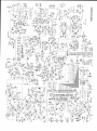
TG550
5 MHz Precision
Function Generator
Service Manual
Book Part Number 48591-0610 - Issue 1
Table of Contents
Specification
3
Safety
6
EMC
7
Installation
8
General
9
Functional Description
11
Circuit Descriptions
12
Calibration
14
Parts List
17
Component Layouts
24
Circuit Diagram
25
2
Specification
Specifications apply at 18º - 28º after one hour warm-up, at maximum output into 50Ω.
FREQUENCY
Frequency Range:
0·005Hz to 5MHz in 7 overlapping decade ranges with adjustment by
coarse and fine verniers.
Vernier Range:
1000:1 on each range.
Frequency Display:
Auto-ranging reciprocal measurement giving 4-digit resolution down to
10Hz (to 1Hz on the 5Hz range); resolution is fixed at 0·01Hz below 10Hz
(0·001Hz below 1Hz on the 5Hz range).
Accuracy is ± 1 digit to 2·1Hz (to 0·21Hz, Symmetry off, or to 0·42Hz,
Symmetry on, on the 5Hz range); below this the accuracy is ± 1% of range
full scale (unspecified with Symmetry on).
Frequency Locking:
With vernier setting between 10% and 100% of range maximum, frequency
can be locked to the crystal reference to maintain it at the displayed value ±
0·01%.
WAVEFORMS
Waveform specifications apply for the top decade of each frequency range.
SINE
Distortion:
Amplitude Flatness:
Less than 0·5% on 500Hz, 5kHz and 50kHz ranges; less than 1% on 5Hz,
50Hz and 500kHz ranges; all harmonics >25dB below fundamental on
5MHz range.
± 0·2dB to 200kHz; ± 2dB to 5MHz.
TRIANGLE
Linearity:
Better than 99% to 200kHz.
SQUAREWAVE
Rise and Fall Times:
Mark-Space Ratio:
<45ns.
1:1 ± 1% to 100kHz.
Range:
± 10V (unterminated).
DC
SYMMETRY
Symmetry Range:
Variable typically between 1:9 and 9:1 (on top decade of each range),
frequency divided by 10 when Symmetry is selected.
MODULATION MODES
Modulation can be used with all waveforms and at any frequency.
Sweep
Sweep Mode:
Internal: linear or logarithmic; sweep Start and Stop frequencies
displayed at a press of a button.
External: linear.
Sweep Width:
Up to 1000:1 within each range.
Sweep Rate:
Internal sweep rate adjustable from typically 20ms to 20s.
External Sweep:
By signal applied by SWEEP IN/OUT socket.
3
Amplitude Modulation
Modulation Depth:
Variable 0 to 100% typical.
Modulation Frequency:
400Hz internal. DC to 100kHz external.
External Modulation:
By signal applied to COUNT/AM IN socket.
OUTPUTS
50Ω Main Out
Output Impedance:
50Ω.
Amplitude:
2mV to 20V peak-peak open circuit (1mV to 10V peak-peak into 50Ω) in
four switch-selectable ranges with 20dB vernier control within each
range.
Attenuator:
0, –20, – 40 or – 60dB.
DC Offset Range:
±10V. DC offset plus signal peak limited to ±10V (±5V into 50Ω); CLIP
shows in display when offset + signal peak exceeds ±10V. DC offset plus
waveform attenuated proportionally by the attenuator.
600Ω Main Out
Alternative output socket providing the same signal as the 50Ω Main Out but from 600Ω. The 50Ω
and 600Ω sockets are not independent.
Aux Out
Output Characteristics:
Frequency, symmetry and phase the same as main outputs.
Output Level:
0 to 5V TTL/CMOS logic levels capable of driving 2 standard TTL loads.
Sweep Out
When internal sweep is selected the sweep signal is available as a 0 to 3V ramp from 600Ω.
INPUTS
Sweep In
The SWEEP IN/OUT socket is set to Sweep In when EXT SWEEP is selected.
Input Impedance:
10kΩ.
Input Sensitivity:
0 to 3V for 1000:1 sweep.
Maximum Allowable
Input Voltage:
± 10V.
Sweep Linearity:
Better than 1%
Maximum Slew Rate of
Sweep Voltage:
0·1V/µs.
AM In
The AM/COUNT IN socket is set to AM input when EXT AM is selected.
4
Input Impedance:
40kΩ.
Input Sensitivity:
Approximately 2V peak-peak for 50% modulation.
Maximum Allowable
Input Voltage:
± 10V.
Count In
The AM/COUNT IN socket is set to external frequency measurement when EXT COUNT is
selected.
Input Impedance:
1MΩ//25pF.
Input Sensitivity:
50mVrms (sinewave).
Maximum Allowable Input
Voltage:
50Vdc/50Vrms to 400Hz with respect to ground
1Vrms above 1MHz.
, reducing to
DISPLAY FUNCTIONS
The LCD shows generator frequency simultaneously with output amplitude/offset, together with
various status annunciators. Alternatively, it is the external frequency measurement display.
Internal Measurement Accuracy
Frequency:
Auto-ranging reciprocal measurement giving 4-digit resolution down to
10Hz (to 1Hz on the 5Hz range); resolution is fixed at 0·01Hz below
10Hz (0·001Hz below 1Hz on the 5Hz range).
Accuracy is ± 1 digit to 2·1Hz (to 0·21Hz, Symmetry off, or to 0·42Hz,
Symmetry on, on the 5Hz range); below this the accuracy is ± 1% of
range full scale (unspecified with Symmetry on).
Amplitude:
Display shows peak-to-peak amplitude or rms value. Display corrected
for attenuator setting. 3-digit resolution, accuracy typically ±5% of
range full scale.
DC Offset:
3-digit resolution; accuracy typically ±2% setting ± 1 digit.
Display corrected for attenuator setting.
External Frequency Measurement
Frequency Range:
5Hz to 20MHz, fully autoranging.
Input Sensitivity:
50mVrms (sinewave).
Measurement Time:
Selectable 0·5s or 5s.
Resolution:
6 digits in 0·5s; 7 digits in 5s.
Accuracy:
± 1 digit ± timebase accuracy.
Timebase Accuracy:
± 10ppm initial error; ±5 ppm/year ageing rate; typically less than
0·5 ppm/ºC.
GENERAL
POWER REQUIREMENTS
AC Input Voltage:
Power Consumption:
Operating Range:
Storage Range:
Environmental:
Size:
Weight:
Safety:
EMC:
230V or 115V nominal, 50/60Hz, by internal adjustment; operating range
± 14% of nominal. Installation Category II.
25VA max.
+5°C to +40°C, 20% to 80% RH.
-10°C to +65°C
Indoor use at altitudes up to 2000m, Pollution Degree 1.
260 (W) x 88 (H) x 235 (D) mm (10.2 x 3.4 x 9.2") excluding handle and
feet.
1.9kg (4.2lb).
Complies with EN61010-1.
Complies with EN50081-1 and EN50082-1.
5
Safety
This instrument is Safety Class I according to IEC classification and has been designed to meet
the requirements of EN61010-1 (Safety Requirements for Electrical Equipment for Measurement,
Control and Laboratory Use). It is an Installation Category II instrument intended for operation
from a normal single phase supply.
This instrument has been tested in accordance with EN61010-1 and has been supplied in a safe
condition. This instruction manual contains some information and warnings which have to be
followed by the user to ensure safe operation and to retain the instrument in a safe condition.
This instrument has been designed for indoor use in a Pollution Degree 1 environment (no
pollution, or only dry non-conductive pollution) in the temperature range 5°C to 40°C, 20% –80%
RH (non-condensing). It may occasionally be subjected to temperatures between +5° and –10°C
without degradation of its safety.
Use of this instrument in a manner not specified by these instructions may impair the safety
protection provided. Do not operate the instrument outside its rated supply voltages or
environmental range. In particular excessive moisture may impair safety.
WARNING! THIS INSTRUMENT MUST BE EARTHED
Any interruption of the mains earth conductor inside or outside the instrument will make the
instrument dangerous. Intentional interruption is prohibited. The protective action must not be
negated by the use of an extension cord without a protective conductor.
When the instrument is connected to its supply, terminals may be live and opening the covers or
removal of parts (except those to which access can be gained by hand) is likely to expose live
parts. The apparatus shall be disconnected from all voltage sources before it is opened for any
adjustment, replacement, maintenance or repair.
Any adjustment, maintenance and repair of the opened instrument under voltage shall be avoided
as far as possible and, if inevitable, shall be carried out only by a skilled person who is aware of
the hazard involved.
If the instrument is clearly defective, has been subject to mechanical damage, excessive moisture
or chemical corrosion the safety protection may be impaired and the apparatus should be
withdrawn from use and returned for checking and repair.
Make sure that only fuses with the required rated current and of the specified type are used for
replacement. The use of makeshift fuses and the short-circuiting of fuse holders is prohibited.
Do not wet the instrument when cleaning it.
The following symbols are used on the instrument and in this manual:Caution - refer to the accompanying documentation, incorrect
operation may damage the instrument.
terminal connected to chassis ground.
alternating current.
6
EMC
This generator has been designed to meet the requirements of the EMC Directive 89/336/EEC.
Compliance was demonstrated by meeting the test limits of the following standards:
Emissions
EN50081-1 (1992) Generic emission standard for residential commercial and light
industry. Test methods and limits used were:
a) EN55022 Conducted, Class B
b) EN55022 Radiated, Class B
Immunity
EN50082-1 (1992) Generic immunity standard for residential, commercial and light
industry. Test methods and limits used were:
a) EN60801-2 (1993) Electrostatic Discharge, 8 kV air discharge.
b) IEC801-3 (1984) RF Field, 3 V/m.
c) IEC801-4 (1988) Fast Transient, 1 kV peak (AC line), 0·5kV peak (signal lines).
Cautions
To ensure continued compliance with the EMC directive the following precautions should be
observed:
a) connect the generator to other equipment using only high quality, double-screened cables.
b) after opening the case for any reason ensure that all signal and ground connections are
remade correctly before replacing the cover. Always ensure all case screws are correctly
refitted and tightened.
c) In the event of part replacement becoming necessary, only use components of an identical
type, see Parts List.
7
Installation
Mains Operating Voltage
The operating voltage of the instrument is shown on the rear panel. Should it be necessary to
change the operating voltage from 230V to 115V or vice-versa, proceed as follows:
1.
Disconnect the instrument from all voltage sources.
2.
Remove the 4 screws which hold the upper and lower case halves together and lift off the
case lower.
3.
Remove the 6 screws securing the main pcb to the case upper and lift the pcb free,
complete with front and rear panels.
4.
Change the appropriate zero-ohm links beside the transformer on the pcb:
Link LK2 only for 230V operation
Link LK1 and LK3 only for 115V operation
5.
Refit the pcb to the case upper, ensuring all connections (especially safety earth) are
remade as before, and refit the case lower.
6.
To comply with safety standard requirements the operating voltage marked on the rear
panel must be changed to clearly show the new voltage setting.
7.
Change the fuse to suit the new operating voltage, see below.
Fuse
The correct time-lag fuse must be fitted for the selected operating voltage.
For 230V operation use 125mA (T) 250V HBC.
For 115V operation use 250mA (T) 250V HBC.
Make sure that only fuses with the required rated current and of the specified type are used for
replacement. The use of makeshift fuses and the short-circuiting of fuse holders are prohibited.
Mains Lead
When a three core mains lead with bare ends is provided it should be connected as follows:
Brown
-
Mains live
Blue
-
Mains Neutral
Green/Yellow
-
Earth
WARNING! THIS INSTRUMENT MUST BE EARTHED
Any interruption of the mains earth conductor inside or outside the instrument will make the
instrument dangerous. Intentional interruption is prohibited.
8
General
Service Handling Precautions
Service work or calibration should only be carried out by skilled engineers. Please note the
following points before commencing work.
The tracks on the printed circuit board are very find and may lift if subjected to excessive heat.
Use only a miniature temperature controlled soldering iron and remove all solder (on both sides of
the joint) with solder wick or suction before attempting to remove a components.
Many of the integrated circuits are CMOS devices and are should be taken when handling to
avoid damage by static discharge.
Dismantling the instrument
1.
Invert the instrument and remove the 4 screws next to the rubber feet.
2.
Lift off the case lower ensuring the front and rear panels stay with the case upper.
3.
Remove the 6 screws securing the main pcb to the case upper and lift the pcb free,
complete with front and rear panels.
4.
To remove the control pcb from the front panel, first pull off the small knobs and unplug
the two flat cable assemblies. Then desolder all other wire connections between main and
control pcbs (at the control board end), lift the assembly clear and undo the 8 screws
which hold the control board to the front panel; the control board can then be removed.
5.
To gain access to the microcontroller the LCD must be removed.
6.
The rear panel can be removed by undoing the tamper-proof safety earth connection.
7.
Reassemble in the reverse order taking care to remake connections exactly as before,
particularly the safety earth wiring.
9
Functional Block Diagram
10
Functional Description
The relationships between the major circuit elements are shown in the block diagram.
The summing amplifier sums the voltages from the dial, the frequency lock DAC, sweep input and
the internal sweep circuit and its output controls the magnitude of the complimentary current
source and current sink. This current varies from approximately 4·3uA to 4·3mA for a 1000:1
frequency change (·005 to 5·0). The symmetry control adjusts the ratio between the current
source and current sink.
The diode gate steers current into and out of the range multiplier capacitor and is controlled by
the comparator output. When the comparator output is high the charge on the capacitor will rise,
linearly, producing the positive going triangle slope. When the comparator output is low the
charge on the capacitor will fall linearly producing the negative going triangle slope.
The triangle amplifier has unity gain and buffers the triangle wave on the multiplier capacitor to
drive the comparator and output circuits.
The comparator operates as a window detector with fixed limit points set to the triangle peaks.
One of its two outputs drives the TTL/CMOS output. The other output is level shifted to drive the
diode gate and squarewave shaper. When the comparator output to the diode gate is high the
triangle wave is positive-going until this reaches approximately +1V, when the comparator output
switches low. When the comparator output is low the triangle wave is negative-going until it
reaches approximately –1V, when the comparator goes high, and the cycle is repeated. This
basic function generator loop is shown by the double arrows in the block diagram. Triangle and
squarewave are generated simultaneously as shown.
To achieve the 500Hz, 50Hz and 5Hz ranges, the 5k range capacitor is multiplied by 10, 100 or
1000 by the capacitor multiplier circuit.
The sinewave converter uses the non-linear characteristics of a transistor pair to convert the
triangle wave into a sinewave. The selected function is amplified by the pre-amp and applied to
the amplitude control directly or via the amplitude modulator. The signal is summed with the
voltage from the DC offset control at the output amplifier, which amplifies the signal up to 20V
peak to peak to drive the main output socket.
The microcontroller measures and displays frequency directly down to 0·2Hz; below this the
microcontroller’s A to D converter measures the voltage at the summing amplifier and displays the
corresponding frequency. Amplitude and offset are measured by the A to D converter too.
The sweep generator provides a triangle wave with variable amplitude and speed that is summed
with the dial at the summing amplifier.
External Count In is amplified by a comparator and measured by the microcontroller.
The power supply converts the incoming AC line voltage to the DC rails required by the
instrument.
11
Circuit Descriptions
Power Supply - DC Regulation
Diode bridge BR2 rectifies the full output of the transformer; C56 and C57 are the reservoir
capacitors which supply the ± 15V regulators. Fine adjustment is provide by VR23 and VR24.
The ± 12V rails are derived from the ± 15V rails with D31 and D32.
The +6V rail is derived from the +15V rail with D33.
IC39 is a 2.5V reference; IC41B generates +5VA, fine adjusted by VR38.
IC41C and D provide ± 12VA.
Diode bridge BR1 rectifies the lower output of the transformer; C131 and C132 are the reservoir
capacitors which supply the ± 5V regulators.
Waveform Generation - Summing Amplifier and Current Sources
The dial and sweep voltages are summed by IC36B; the output range of the amplifier is
approximately –4mV to –4V for a 1000:1 frequency change. Q1 gives increased current capability
to drive R24 and R76. When the symmetry button is depressed R24 and R76 are increased by a
factor of 10 with the symmetry control in mid-position, decreasing the output frequency by a factor
of 10. This allows a symmetry range of 10:1.
IC2C refers the output of IC36B to the +12V rail; IC4 and Q4 mirror this into the diode gate.
IC2A inverts the output of IC36B, IC2B refers it to the –12V rail, IC22 and Q18 mirror this into the
diode gate.
Waveform Generation - Range Selection and Triangle Amplifier
Ranges 5kHz to 5MHz use decade steps of range capacitor. The lower three ranges use a
capacitance multiplier. The capacitance multiplier steals current from the capacitor via R101.
The triangle amplifier uses Q7 as a source follower and Q8 as a current source; Q7 and Q8 are
Idss matched. Q9 and Q10 are emitter followers to give two low impedance outputs. The stage
has unity gain and the offset is trimmed by VR14.
Waveform Generation - Comparator and Aux Output
IC5 operates as a window detector and determines the peak to peak amplitude of the triangle
wave on the range capacitor, which is approximately ± 1V. Capacitors C15 to C20 compensate for
comparator delay ensuring that the triangle wave amplitude remains constant with increase in
frequency. The two internal NAND gates in IC5 are wired as a flip-flop to ensure positive
switching of the comparator.
Q6 level shifts the output of IC5 to be about ground, to drive the diode gate. IC6 drives the Aux
Output with a TTL/CMOS compatible signal.
Waveform Generation - Waveform Shaping
The sine shaper comprises a monolithic transistor array IC17 which is driven by the triangle
amplifier. The circuit has two non-linear stages. A pair of emitter followers A and D round the
peaks of the triangle; the output of this stage is impressed across R103 and R108 in series and
applied to the second stage. This comprises a differential pair B and C driven almost into cut-off
and converts the clipped triangle into a sinewave. VR10 adjusts the gain of this pair to bring them
close to cut off, minimising sinewave distortion. VR11 adjusts the dc operating point of the
sinewave converter to give symmetrical operation on both positive and negative halves of the
waveform.
The squarewave shaper is a diode bridge D36 to D39, driven by a level shifter Q26, which steers
current into and out of R91 and C32. This gives a clean waveform which is symmetrical about
ground. When squarewave is not selected SW10A gates the signal off at IC6B.
Preamplifier
The waveform selected by IC14 passes to the preamplifier IC18. The 1·8V pk to pk output is
connected to the Amplitude control via the AM switch.
12
Output Amplifier
Q21 and Q22 are complementary emitter followers and buffer the output of IC19.
The DC Offset control is buffered by IC23A and IC23C and applied via R120 and R175.
Amplitude Modulator
When the AM button is depressed, the amplitude modulator is inserted between the preamplifier
and the output amplifier. IC21 is a balanced modulator. IC24 is a differential amplifier which
amplifies the difference between the open collector outputs of IC21. The circuit around IC37
forms a 400Hz oscillator the output is passed through a Sallen and Key low pass filter IC20B.
IC20A buffers the signal on the modulation depth control VR33 and also sets the dc bias for IC21.
Sweep – Ramp Generator
The rate control VR31 determines the magnitude of the current source IC7A and Q12. This
current is steered into and out of C25 by the operational transconductance amplifier (OTA) IC8.
The voltage on C25 is buffered by IC7B to drive the stop control VR35 and the window
comparator IC10A and IC10B. The thresholds of the window comparator determine the limits of
the ramp which are 0V and +4V. Q13 and Q14 are level shifters to drive flip flop IC12A. The
output of IC12A is level shifted by R74 and R57 and clamped by D5 and D4 to be symmetrical
about 0V. When the input to IC8 is high the OTA sources current into C25; when the input is low
the OTA sinks current from C25. This loop is very similar to a function generator. If either the set
start or set stop buttons are depressed the loop is closed around the ramp generator forcing the
ramp to be held precisely at its lower or upper limit. IC10D buffers the signal on VR21 to drive the
main board directly or via the log converter.
Sweep – Log Converter
IC3D sums the output of the ramp generator with an offset current to drive the logging transistors
IC13A and IC13B. Temperature compensation of the log converter is by TDR1 which has a
temperature coefficient of +0·3%/°C. The log converter itself simply uses the exponential
relationship between Vbe and collector current. IC13 is a matched transistor array. The
right-hand transistor is the logging transistor and its emitter is driven by the input voltage via the
left-hand transistor which compensates for the logging transistor Vbe. The left hand transistor’s
collector current is defined by R16 and is held constant by IC3A; its Vbe is therefore constant and
so the input voltage at the junction of R19 and TDR1 is impressed across the Vbe of the logging
transistor. The logarithmic change in collector current of the logging transistor is converted into a
voltage by IC3B. The log converter is actually an antilog converter.
Digital Display
IC30 is a microcontroller that provides frequency and voltage measurement and displays the
results on the LCD. In frequency measurement mode IC29-A outputs the GATE signal, which is
controlled via the J (START) and K (STOP) inputs. The GATE is synchronised to the positive
edges of the input signal. Whilst GATE is high IC30 counts the internal reference clock and
IC29-B outputs the input signal divided by two, which is also counted by IC30. When GATE goes
low the frequency is calculated and displayed.
Voltage measurements are made via the A-D inputs RA0 (pin 5), RA1 (pin 6) and RA3 (pin 9).
RA0 input measures the amplitude voltage (VA). RA1 input measures the Frequency Dial voltage
(VF) which is used to display low frequency measurements. RA3 input measures the offset
voltage (VOFT).
IC31 is a DAC that outputs a correction voltage to IC3-C when frequency lock is selected. This
correction voltage is adjusted by IC30 to maintain frequency lock.
IC35 and IC38 are multiplexers that are used by IC30 to input the instrument status; IC30
updates the display with the correct settings.
13
Calibration
Equipment Required
Oscilloscope
Distortion Meter
4·5 digit Multimeter
Reciprocal counting Frequency Meter
Only the case lower need be removed to gain access to all adjustments. Allow 1 hour warm-up
(with the case lower in place) before commencing. For best results, use the following procedure.
1.
2.
Power Supply
+15V ± −20mV - VR23
−15V ± 20mV - VR24
+12V ± 0·5V
−12V ± −0·5V
+5V ± 0·25V
−5V ± −0·3V
+5VA ± 20mV - VR38
+6V ± 0·5V
Offset Nulling
Select: 5k range, frequency vernier to 3·0, sweep OFF.
IC
TP
Adjust
DVM Reading
4
2
VR6
<40µV
22
3
VR7
<40µV
16
6
VR13
<40µV
3.
Nulling of the triangle amplifier is achieved by shorting its input (TP5) and adjusting VR14
to give <2mV on TP4.
4.
Preamplifier and Output Amplifier DC Offsets
Ensure that the DC offset control is at its centre detent. Release all three function buttons.
Amplitude control to minimum, adjust VR16 for <5mV at the main output.
Amplitude control to maximum, adjust VR15 for <5mV at the main output.
5.
Waveform Symmetry
5k range, vernier at approximately 4, squarewave, adjust VR8 for equal mark:space ratio
using the oscilloscope x10 X-multiplier to increase resolution and the trigger slope switch.
5M range, vernier to approximately ·005 to give 5kHz to 6kHz, adjust VR5 for equal
mark:space ratio.
6.
Frequency Calibration
Connect the Frequency Counter to AUX output.
Select external count and apply a frequency standard to AM/COUNT IN, select 5 sec gate
time if required and adjust VC2 through the front panel for the correct reading ± 2 ppm.
Select internal count and remove the frequency standard.
Dial fully clockwise, 5kHz range, note the reading on the internal frequency counter.
500Hz range, adjust VR12 for one tenth of the above reading ± 5 digits.
5kHz range, adjust verniers for 5Hz.
50Hz range, adjust VR36 for 00·05.
Fit shorting link to TP1 and adjust the verniers for 18·0Hz on the external counter.
Adjust VR37 for 1·80 on the display.
Remove TP1 short.
14
7.
Sinewave Distortion
Select sinewave, 5k range, 3kHz. Adjust VR10 and VR11 for minimum distortion. Adjust
VR9 for the output to be symmetrical about 0V.
8.
AM
500k range, approximately 300kHz, sinewave, modulation to minimum, amplitude to
maximum (20V pk-pk).
Select AM, check output drops to half (10V pk-pk) adjusted by VR18.
Modulation to maximum, adjust VR17 for 100% modulation.
Release all 3 function buttons, increase the oscilloscope gain and adjust VR19 for
minimum output of the 400Hz modulation source.
Adjust VR20 for 0V ± 50mV output. Turn AM off.
9.
Meter Calibration
Calibration of the frequency meter was covered in 6 above.
Display select to amplitude, 5k range, squarewave, adjust the amplitude control to give
16V pk-pk (8V pk-pk into 50Ω) then adjust VR28 on the control board for 1600 on the
display.
Display select to offset, release all 3 function buttons, amplitude to minimum, offset control
at centre detent, connect a multimeter to the main output, adjust VR22 so that both meters
read the same.
Offset control fully clockwise, adjust VR21 so both meters read the same, ±1%.
10.
Sweep
Sweep to ON, LIN stop control to maximum, 5M range, vernier to minimum (·005), hold in,
set start and adjust VR2 for 4·3kHz to 4·8kHz. Select LOG, hold in set start and adjust
VR4 for 4·3kHz to 4·8kHz. Select 500k range, hold in, set stop and adjust VR3 for
500kHz.
VR34 on the display board adjusts display contrast.
11.
Power Consumption
230V <100mA
115V <200mA
Control Board – Calibration Points
15
Main Board – Calibration Points
16
Parts List
PCB ASSY MAIN (44912-0450)
Part No.
Description
Position
20205-0610
STUD M3 X 10 KFH-M3-10ET
FOR PJ2
20613-0007
WASHER (SIL-PAD) TO220 PLAIN
FOR IC25,26
20661-0801
SPACER TRANSISTOR MTG TO5
FOR Q21,22
20670-0040
HEATSINK TO5 48DEG C/W
FOR Q21,22
20670-0135
CLIP GP02 FOR PCB MTG H/SINKS
FOR IC25,26
20670-0320
HEATSINK PCB MTG 50MM PLAIN
FOR IC25,26
22040-0901
BEAD FERRITE FX1115
FB1-5
22115-0390
TRANSFORMER
T1
22219-0120
SWITCH ROCKER SPST R/A
PCB MNT SW26
22225-0760
SWITCHBANK X 13
SW1-13
22312-0260
FUSEHOLDER PCB MOUNT
FOR FS1
22315-0239
FUSE 125MA TL HRC
FS1
22315-0450
FUSE 500mAT SUBMIN PCB MNT
FS2-5
22520-0160
AC RECEP 10AMP R/ANG
PJ2
22573-0041
HEADER 2 WAY STRAIGHT
TP1-6
22573-9110
HEADER 36W STR SIL TIN
PJ6 (9 WAY), PJ7 (5 WAY)
22575-0064
HEADER 26 WAY (2X13) STR SKEL
PJ1
22575-0103
HEADER 16 WAY (2X8) STR SKELTN
PJ5
23185-0000
RES ZERO OHM
LK2
23185-6120
RES 12M0J W25 CF
R4
23202-0100
RES 10R0F W25 MF 50PPM
R92
23202-0270
RES 27R0F W25 MF 50PPM
R53
23202-0470
RES 47R0F W25 MF 50PPM
R31,102,112,144
23202-0750
RES 75R0F W25 MF 50PPM
R163
23202-0910
RES 91R0F W25 MF 50PPM
R118
23202-1100
RES 100RF W25 MF 50PPM
R10,35,90,148,149
23202-1120
RES 120RF W25 MF 50PPM
R116,162
23202-1124
RES 124RF W25 MF 50PPM
R43,44
23202-1150
RES 150RF W25 MF 50PPM
R48,58,65
23202-1180
RES 180RF W25 MF 50PPM
R110
23202-1191
RES 191RF W25 MF 50PPM
R91
23202-1200
RES 200RF W25 MF 50PPM
R128-131
23202-1220
RES 220RF W25 MF 50PPM
R38,41,46,119,179,180
23202-1226
RES 226RF W25 MF 50PPM
R108
23202-1330
RES 330RF W25 MF 50PPM
R36
17
PCB ASSY MAIN (44912-0450) continued/…
Part No.
Description
Position
23202-1340
RES 340RF W25 MF 50PPM
R106
23202-1402
RES 402RF W25 MF 50PPM
R229
23202-1470
RES 470RF W25 MF 50PPM
R37
23202-1510
RES 510RF W25 MF 50PPM
R155,156
23202-1620
RES 620RF W25 MF 50PPM
R24,25,75,76
23202-1680
RES 680RF W25 MF 50PPM
R114
23202-1681
RES 681RF W25 MF 50PPM
R42,45
23202-1715
RES 715RF W25 MF 50PPM
R26,29,77
23202-1820
RES 820RF W25 MF 50PPM
R32,121
23202-1910
RES 910RF W25 MF 50PPM
R30,83
23202-2100
RES 1K00F W25 MF 50PPM
R33,49,84,88,101,158
23202-2110
RES 1K10F W25 MF 50PPM
R103
23202-2120
RES 1K20F W25 MF 50PPM
R34
23202-2137
RES 1K37F W25 MF 50PPM
R82
23202-2143
RES 1K43F W25 MF 50PPM
R78,81
23202-2150
RES 1K50F W25 MF 50PPM
R39,40,89,122,126
23202-2160
RES 1K60F W25 MF 50PPM
R120,175
23202-2180
RES 1K80F W25 MF 50PPM
R52,
23202-2200
RES 2K00F W25 MF 50PPM
R115,161
23202-2220
RES 2K20F W25 MF 50PPM
R17,59,74,87,159,171,172,176,177,
178,181-183,186,187,227,238
23202-2249
RES 2K49F W25 MF 50PPM
R136
23202-2300
RES 3K00F W25 MF 50PPM
R50,54,150
23202-2402
RES 4K02F W25 MF 50PPM
R63,152
23202-2430
RES 4K30F W25 MF 50PPM
R21,231
23202-2510
RES 5K10F W25 MF 50PPM
R226
23202-2560
RES 5K60F W25 MF 50PPM
R157
23202-2665
RES 6K65F W25 MF 50PPM
R147
23202-2680
RES 6K80F W25 MF 50PPM
R153,233
23202-2750
RES 7K50F W25 MF 50PPM
R18,232
23202-3100
RES 10K0F W25 MF 50PPM
R1,8,11,13,14,23,60,61,66,68, 70-72,
79, 85, 86, 93, 96, 98, 107, 142, 146,
164,168,170,173,207,239
23202-3107
RES 10K7F W25 MF 50PPM
R19
23202-3110
RES 11K0F W25 MF 50PPM
R2,62,138,139,140
23202-3120
RES 12K0F W25 MF 50PPM
R12,151,167
23202-3127
RES 12K7F W25 MF 50PPM
R47,
PCB ASSY MAIN (44912-0450) continued/…
18
Part No.
Description
Position
23202-3130
RES 13K0F W25 MF 50PPM
R145,223
23202-3150
RES 15K0F W25 MF 50PPM
R57,105,109,113
23202-3220
RES 22K0F W25 MF 50PPM
R97,165,184,235
23202-3226
RES 22K6F W25 MF 50PPM
R104
23202-3249
RES 24K9F W25 MF 50PPM
R111
23202-3270
RES 27K0F W25 MF 50PPM
R22
23202-3300
RES 30K0F W25 MF 50PPM
R16,69,154,234
23202-3330
RES 33K0F W25 MF 50PPM
R15,185
23202-3360
RES 36K0F W25 MF 50PPM
R3,228
23202-3390
RES 39K0F W25 MF 50PPM
R7,9
23202-3430
RES 43K0F W25 MF 50PPM
R143
23202-3470
RES 47K0F W25 MF 50PPM
R55,141
23202-3510
RES 51K0F W25 MF 50PPM
R6
23202-3560
RES 56K0F W25 MF 50PPM
R117,169
23202-4100
RES 100KF W25 MF 50PPM
R27,28,64,94,166,188,230
23202-4110
RES 110KF W25 MF 50PPM
R225
23202-4180
RES 180KF W25 MF 50PPM
R56
23202-4270
RES 270KF W25 MF 50PPM
R80,224
23202-5100
RES 1M00F W25 MF 50PPM
R95,189
23202-5470
RES 4M70F W25 MF 50PPM
R20
23202-6100
RES 10M0F W25 MF 50PPM
R5,174
23206-0102
RES 10R2F W60 MF 50PPM
R134
23206-0412
RES 41R2F W60 MF 50PPM
R132,133
23206-0510
RES 51R0F W60 MF 50PPM
R135,137
23206-1600
RES 600RF W60 MF 50PPM
R73
23215-3100
RES 10K0B W25 MF 15PPM
R236,237
23222-0100
RES 10R0J W33 MF FUSIBLE NFR25
R9
23377-1100
RES PS/H 100R CF 10MM
VR8
23377-1470
RES PS/H 470R CF 10MM
VR14,20,23,24
23377-2100
RES PS/H 1K0 CF 10MM
VR12,38
23377-2220
RES PS/H 2K2 CF 10MM
VR21
23377-3100
RES PS/H 10K CF 10MM
VR3,6,7,9,13,18,22,37
23377-3220
RES PS/H 22K CF 10MM
VR2,4,5,11,19,36
23377-3470
RES PS/H 47K CF 10MM
VR15,16,17
23379-1100
RES PS/H 100R CERMET 10mm skel
VR10
23387-1680
RES 680RJ .25S TEMPERATURE DEP
TDR1
PCB ASSY MAIN (44912-0450) continued/…
19
Part No.
Description
Position
23424-0443
CAP 10NZ 1KV CER D10 P5
C55,130
23424-0459
CAP 4N7 250V AC CER STR/LNG Y
C124,125
23427-0268
CAP 22PJ 100V CER NPO P2.5
C17,32,112,113,121
23427-0331
CAP 1N0K 63V CER HI K P5T
C135
23427-0385
CAP 39PJ 100V CER NPO P2.5
C109
23427-0593
CAP 82PG 100V CER NPO P2.5
C16,18
23427-9205
CAP 47PJ 100V CER NPO P2.5
C11
23427-9236
CAP 18PJ 100V CER NPO P2.5
C15
23428-0100
CAP 10PG 100V CER NPO P2.5
C3,23,26,27,28,88,89
23428-1100
CAP 100PG 100V CER NPO P2.5
C2,111,136
23557-0647
CAP 10U 35V ELEC RE2 P2
C53,54,60-66,94,95,117,137,138
23557-0664
CAP 1000U 35V ELEC RE2 P5
C56,57,131,132
23620-0236
CAP 1N0K 100V P/E P5
C68
23620-0245
CAP 4N7K 63V P/E P5
C38
23620-0246
CAP 100NK 63V P/E P5
C1,4,10,12-14,21,22,29-31,34,36,37,
41-52,67,90,91,96-98,101105,108,119,
120,123,139,140
23620-0252
CAP 2N2K 63V P/E P5
C40
23620-0256
CAP 1U0K 63V P/E P5
C25
23620-0266
CAP 680NK 63V P/E P5
C118
23620-9007
CAP 10NK 100V P/E P5
C39
23662-0110
CAP 100NK 63V P/C P5
C35
23662-0203
CAP 150PJ 100V P/C FKC2 P5
C5
23662-0205
CAP 330PK 100V P/C FKC2 P5
C7
23662-0240
CAP 1N50J 100V P/C FKC2 P5
C6
23662-0300
CAP 3N3J 100V P/C P5
C19,20
23662-0310
CAP 22N0J 100V P/C P5
C8
23662-0330
CAP 220NJ 100V P/C P5
C9
25021-0901
DIO 1N4148 B/R
D1-7,12-19,27,28,35
25031-0020
DIO BAT81
D8-11,36-39
25115-0907
DIO 1N4002 B/R
D29,30,43,44
25130-0911
DIO ZEN 3V0 W4
D31,32
25130-9202
DIO ZEN 9V1 W5
D33
25130-9206
DIO ZEN 6V8 W5
D22
25211-9302
RECTIFIER BRIDGE W02G
BR1,2
25336-5590
TRAN PNP BC559C
Q1,2,4,9,10,11,12,17,20
25344-0500
TRAN PNP 2N2905A
Q22
PCB ASSY MAIN (44912-0450) continued/…
20
Part No.
Description
Position
25377-0700
TRAN NPN 2N2219A
Q21
25377-5490
TRAN NPN BC549C
Q3,5,13-16,18,19,26
25381-0404
TRAN NPN 2N3904T
Q6
25601-0103
TRAN FET BF245AT
Q7,8
25601-0400
TRAN MOSFET N CHAN ZVN3306A
Q25
27106-0505
IC CA3080E
IC8
27106-0506
IC LM324N1
IC2,3,10,41
27106-0513
IC LM358N
IC36
27106-0518
IC MC3403P
IC23
27106-0548
IC TSH10IN
IC18,24
27106-0604
IC TL071CP
IC15,16
27106-0606
IC TL072CP
IC7,20
27106-0608
IC LF351N
IC4,22
27106-0641
IC CLC430A
IC19
27151-0110
IC MC1496P
IC21
27160-0009
IC V/REG 7805
IC27
27160-0014
IC V/REG 7905
IC28
27160-0200
IC V/REG LM317
IC25
27160-0210
IC V/REG LM337
IC26
27160-0900
IC V/REG 431
IC39
27164-0503
IC CA3046
IC13,17
27223-0740
IC 74LS74
IC12
27226-0110
IC 4011B
IC37
27226-0530
IC 4053B
IC1,9
27229-0000
IC 74HCT00N
IC6
27230-0520
IC 74HC4052
IC14
27254-0010
IC NE521N
IC5
35555-2730
PCB – MAIN
PCB ASSY – CONTROL (44912-0460)
Part No.
Description
Position
22225-0220
SWITCH PUSH/PUSH SPPH11470B
SW15-19
22226-0101
KEYSWITCH – ALPS SKHHBW
SW20-25
23105-2470
RES SM0805 4K70F W1
R242-247
23202-0270
RES 27R0F W25 MF 50PPM
R201
23202-1100
RES 100RF W25 MF 50PPM
R215
PCB ASSY – CONTROL continued/…
21
Part No.
Description
Position
23202-1150
RES 150RF W25 MF 50PPM
R200
23202-2100
RES 1K00F W25 MF 50PPM
R211,217,218,222
23202-2220
RES 2K20F W25 MF 50PPM
R203
23202-2470
RES 4K7OF W25 MF 50PPM
R216
23202-3100
RES 10K0F W25 MF 50PPM
R204,205,206,240,241
23202-3300
RES 30K0F W25 MF 50PPM
R212,221
23202-4100
RES 100KF W25 MF 50PPM
R214,219
23202-4200
RES 200KF W25 MF 50PPM
R220
23202-5100
RES 1M00F W25 MF 50PPM
R213
23377-1220
RES PS/H 220R CF 10MM
VR28
23377-3100
RES PS/H 10K CF 10MM
VR34
23347-0140
POT 10K LIN VO12L-PV25F-B10K
VR27,32,33,35
23347-0350
POT 500K LOG FLAT SHAFT 25MM
VR31
23347-0360
POT 10K LIN DETENT FLAT SHAFT
VR26
23347-0530
POT 1K + 1K GANGED V/PCB MOUNT
VR30
23427-9209
CAP 33PJ 100V CER NPO P2.5
C70
23427-9205
CAP 47PJ 100V CER NPO P2.5
C71
23450-0036
CAP 47PK 500V 5MM DIA P5
C74
23461-0020
CAP SM0805 100NZ 50V CER Y5V
C72,78-86,115,142,144-146
23557-0505
CAP 10U 16V ELEC RC2 P1.5
C76,141,143
23557-0658
CAP 100U 25V ELEC RE2 P2.5
C75
23633-0002
CAP 100NJ 250V P/E UNCOAT P7.5
C73
23984-0017
TRIMCAP 4-20P 5MM GREEN
VC2
25021-0901
DIO 1N4148 B/R
D42,47
25030-0905
DIO BA482 B/R
D40,41
25601-9007
TRAN FET (NJ) J309
Q24
25061-0200
LED – T1 ROUND (3MM) – RED
LED1,2
26100-0220
LCD
LCD1
27153-1040
IC SM TLC5615CD 10-BIT DAC
IC31
27236-0530
IC SM 74HC4053
IC34
27238-0000
IC SM 74HCT00
IC33
27239-1070
IC SM 74HC107
IC29
27239-1510
IC SM 74HC151
IC35,38
27250-2110
IC SM PIC16C924-08L PLCC
IC30
27254-1008
IC SM 75107
IC32
28500-9008
XTAL – 8MHZ – MICROPROCESSOR
XTL1
35555-2740
PCB – CONTROL
CASE PARTS
22
Part No.
Description
Position
20038-9502
WASHER M4 SPRING
REAR PANEL EARTH
20038-9501
WASHER M3 SPRING
MAIN PCB/CASE UPPER, CONTROL
PCB/FRONT PANEL, FRONT PANEL EARTH
20037-0401
SOLDER TAG SHAKEPROOF - 4BA
REAR PANEL EARTH
20037-0400
SOLDER TAG SHAKEPROOF - 6BA
FRONT PANEL EARTH
20030-0266
WASHER M4 ZPST
REAR PANEL EARTH
20030-0263
WASHER M3 ZPST
FEET, FRONT PANEL EARTH
20065-0030
SCREW N0 4 X 3/8 PLASTT PNHDPZ
MAIN PCB/CASE
20210-0102
NUT M4 ZPSTREAR PANEL
EARTH
20210-0101
NUT M3 ZPST
REAR PANEL EARTH
20662-0540
FOOT MOULDED GREY
20234-0027
SCREW M3 X 6 PNHDPZ ZPST
CONTROL PCB/FRONT PANEL
20236-0010
SCREW M4 X 12 TAMPERPROOF
REAR PANEL EARTH
20661-0258
SPACER Rnd 7/32 IDx1/4 L Nyl
MAIN PCB/CASE UPPER
20612-0011
WASHER FIBRE M3
MAIN PCB/CASE UPPER, CONTROL
PCB/FRONT PANEL
23202-1549
RES 549RF W25 MF 50PPM
OUTPUTS
22491-0120
MAINS LD 2M ST IEC/UK PLUG 5A
FOR UK
22491-0270
MAINS LD 2M ST IEC/EURO PLUG
FOR EUROPE
22588-0004
BNC SKT BKHD 50R STANDARD
23348-0701
WASHER SHK/PROOF
23347-0175
POT 10KA OW20BU F11 X 15
33331-4980
REAR PANEL PRINTED
33331-4970
OVERLAY FRONT PANEL
33331-4960
FRONT PANEL
33536-3820
CASE LOWER - RFI SCREENED
33536-3810
CASE UPPER - RFI SCREENED
31336-0250
HANDLE BENCH INST CASE
37113-2010
KEYCAP
37113-0400
BUTTON, MID-GREY ABS
37151-0390
KNOB 12.5MM D-SHAFT MID GREY
37151-0380
KNOB 21MM D-SHAFT MID GREY
37113-0170
BUTTON, SWITCHBANKS, MID-GREY
48591-0560
INSTRUCTION BOOK
23
Component Layouts
24
Circuit Diagram
25
Thurlby Thandar Instruments Ltd
Glebe Road, Huntingdon, Cambridgeshire PE29 7DR, England
Telephone: (44) 01480 412451 Fax: (44) 01480 450409
e mail: [email protected] web site: www.tti-test.com