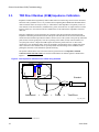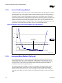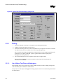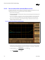
1
R Printed Circuit Board (PCB) Test Methodology User Guide Revision 1.6 January 2000 Order Number: 298179 - 001 Printed Circuit Board (PCB) Test Methodology R Information in this document is provided in connection with Intel products. No license, express or implied, by estoppel or otherwise, to any intellectual property rights is granted by this document. Except as provided in Intel’s Terms and Conditions of Sale for such products, Intel assumes no liability whatsoever, and Intel disclaims any express or implied warranty, relating to sale and/or use of Intel products including liability or warranties relating to fitness for a particular purpose, merchantability, or infringement of any patent, copyright or other intellectual property right. Intel products are not intended for use in medical, life saving, or life sustaining applications. Intel may make changes to specifications and product descriptions at any time, without notice. Designers must not rely on the absence or characteristics of any features or instructions marked "reserved" or "undefined." Intel reserves these for future definition and shall have no responsibility whatsoever for conflicts or incompatibilities arising from future changes to them. The Printed Circuit Board (PCB) Test Methodology may contain design defects or errors known as errata which may cause the product to deviate from published specifications. Current characterized errata are available on request. Contact your local Intel sales office or your distributor to obtain the latest specifications and before placing your product order. I2C is a 2-wire communications bus/protocol developed by Philips. SMBus is a subset of the I2C bus/protocol and was developed by Intel. Implementations of the I2C bus/protocol may require licenses from various entities, including Philips Electronics N.V. and North American Philips Corporation. Alert on LAN is a result of the Intel-IBM Advanced Manageability Alliance and a trademark of IBM Copies of documents which have an ordering number and are referenced in this document, or other Intel literature, may be obtained from: Intel Corporation www.intel.com or call 1-800-548-4725 *Third-party brands and names are the property of their respective owners. Copyright © Intel Corporation 2000 2 User Guide Printed Circuit Board (PCB) Test Methodology R Contents 1. Introduction ...................................................................................................................................7 1.1. 2. Test Structures .............................................................................................................................9 2.1. 3. 3.3. 3.4. 3.5. 3.6. General Equipment ........................................................................................................13 General Calibration ........................................................................................................14 3.2.1. Calibration Sequence ........................................................................................15 3.2.2. General Calibration Verification.........................................................................15 TDR Direct Rambus(28 Ω) Impedance Calibration .......................................................16 3.3.1. Direct RambusStandard Example.....................................................................17 3.3.2. Airline- 28 Ohm (Preferred) ...............................................................................17 3.3.3. Airline- 25 Ohm .................................................................................................17 Probing Techniques .......................................................................................................18 3.4.1. Handheld Probes...............................................................................................19 3.4.2. SMA Connectors ...............................................................................................20 3.4.3. Controlled Impedance Microprobes ..................................................................21 Impedance Measurement Techniques ..........................................................................23 3.5.1. Display Adjustment............................................................................................23 3.5.2. Cursor Positioning Method ................................................................................24 3.5.3. Averaging Mean Method (Preferred).................................................................24 3.5.4. Filter Option .......................................................................................................25 3.5.5. Differential Impedance ......................................................................................26 Velocity Measurement Techniques ................................................................................27 3.6.1. TDR Method ......................................................................................................27 3.6.2. TDT Method ......................................................................................................28 Appendix A: Intel - Direct RambusImpedance Measurement Procedure for Tektronix* ............31 4.1. 4.2. 4.3. 4.4. User Guide Requirements for Matching Test Coupon to Bus Design.................................................9 2.1.1. Impedance Test Coupon General Guidelines ...................................................10 2.1.2. Propagation Velocity Test Coupon General Guidelines ....................................10 Impedance and Velocity Measurement Techniques...................................................................13 3.1. 3.2. 4. Overview ..........................................................................................................................7 Equipment Required ......................................................................................................31 General Setup ................................................................................................................32 4.2.1. Initialize..............................................................................................................33 4.2.2. Instrument Calibration .......................................................................................34 Display Adjustment ........................................................................................................34 4.3.1. Measurement ....................................................................................................36 TDR Direct Rambus(28 Ohm) Impedance Calibration ..................................................37 4.4.1. Airline- 28 Ohm(Preferred) ................................................................................39 4.4.2. Airline- 25 Ohm .................................................................................................39 3 Printed Circuit Board (PCB) Test Methodology R 5. Appendix B: CITS500s Procedure for Rambus Impedance Measurement.............................. 41 5.1. 5.2. 5.3. 5.4. 5.5. 6. Appendix C: Hewlett-Packard* Direct Rambus* Impedance Measurement Procedure............. 61 6.1. 6.2. 6.3. 4 Equipment ..................................................................................................................... 41 Connection..................................................................................................................... 42 Line Length .................................................................................................................... 42 Section 1 – CITS500s (32-bit) ....................................................................................... 43 5.4.1. Horizontal Standardisation ................................................................................ 43 5.4.2. Test File ............................................................................................................ 43 5.4.2.1. Tested Area ........................................................................................ 43 5.4.3. Testing .............................................................................................................. 44 5.4.3.1. Datalogging and SPC Analysis ........................................................... 44 5.4.3.2. Guidelines when using the CITS500s................................................. 45 5.4.4. Verification at 28 Ohm Impedance ................................................................... 47 5.4.4.1. Verification at 28 Ohms ...................................................................... 48 5.4.4.2. Calibration at 28 Ohms ....................................................................... 48 5.4.5. Verification and Calibration at the Probe Tip .................................................... 50 5.4.5.1. Verification .......................................................................................... 50 5.4.5.2. Calibration........................................................................................... 50 Section 2 – CITS500s (16-bit) ....................................................................................... 51 5.5.1. Horizontal Standardisation ................................................................................ 51 5.5.2. Test File ............................................................................................................ 53 5.5.2.1. Tested Area ........................................................................................ 53 5.5.3. Testing .............................................................................................................. 54 5.5.3.1. Use of Macro Test Files and Datalogging........................................... 54 5.5.3.2. Guidelines when using the CITS500s................................................. 55 5.5.4. Verification at 28 Ohm Impedance ................................................................... 57 5.5.4.1. Verification Procedure ........................................................................ 58 5.5.4.2. Alternative Method .............................................................................. 59 Equipment ..................................................................................................................... 61 General Setup................................................................................................................ 61 6.2.1. Instrument/Plug-in Module Calibration.............................................................. 62 6.2.2. Hardware Setup and Initialize ........................................................................... 63 6.2.3. Display Adjustment ........................................................................................... 64 6.2.3.1. Measurement Overview...................................................................... 67 6.2.3.2. Normalization (Recommended) Procedure ........................................ 68 6.2.3.3. Offset (alternate) Procedure ............................................................... 71 6.2.4. Coupon Measurement ...................................................................................... 73 6.2.4.1. Normalized (preferred) Measurements............................................... 73 6.2.4.2. Non-normalized offset (alternate) Measurements .............................. 74 TDR Rambus Calibration Re-Verification and Drift ....................................................... 75 6.3.1. Precision Normalization and Verification Standards ......................................... 76 User Guide Printed Circuit Board (PCB) Test Methodology R Figures Figure 1. Example SMA Test Structure Including Flood/Dummy Traces ...................................9 Figure 2. Sample Impedance and Velocity Test Structures for 28 Ω Microstrip.......................11 Figure 3. Sample Impedance and Velocity Test Structure for 28 Ω Stripline Design ...............14 Figure 4. Low impedance calibration error offset using standard.............................................16 Figure 5. 25 Ω calibration with two 50 Ω airlines ......................................................................18 Figure 6. Example Handheld Probe with Ground Spanner.......................................................18 Figure 7. Handheld Ground Mechanisms Illustrating Ground Loop Differences ......................19 Figure 8. Handheld Probe (short vs long ground loop measuring the same test coupon) .......19 Figure 9. SMA Probe Example .................................................................................................20 Figure 10. Comparison of Handheld and SMA Probing Techniques........................................21 Figure 11. Microprobe Example................................................................................................21 Figure 12. Comparison of Microprobe and SMA TDR Responses...........................................22 Figure 13. Comparison of Microprobe and SMA Edge Rate Degradation................................22 Figure 14. Example Screen Display When Measuring 28 Ω Coupons.....................................23 Figure 15. Example of the Cursor Positioning Method on a TDR Response ...........................24 Figure 16. Example of Averaging Mean Method for a 28 Coupon ...........................................25 Figure 17. Comparison on Unfiltered vs Filtered (200 ps) Response.......................................26 Figure 18. Example of a Differential Impedance TDR Response.............................................27 Figure 19. Example of a Velocity Measurement Using the TDR Method .................................28 Figure 20. Example of a Basic TDT Setup ...............................................................................29 Figure 21. Example Delay Measurement using TDT Approach ...............................................29 Figure 22. Typical Test File Editor display................................................................................44 Figure 23. Open-circuit display using IP-28..............................................................................45 Figure 24. Typical measurement using IP-28...........................................................................46 Figure 25. Open-circuit display using IP-50..............................................................................46 Figure 26. Typical measurement using IP-50...........................................................................47 Figure 27. Typical display during 28 Ohm Verification .............................................................49 Figure 28. Typical display during 28 Ohm Calibration ..............................................................49 Figure 29. Typical display before Horizontal Standardisation...................................................52 Figure 30. Typical display after Horizontal Standardisation......................................................52 Figure 31. Typical Test File Editor display (using IP-28) ..........................................................53 Figure 32. Typical Test File Editor display (using IP-50) ..........................................................54 Figure 33. Open-circuit display using IP-28..............................................................................55 Figure 34. Typical measurement using IP-28...........................................................................56 Figure 35. Open-circuit display using IP-50..............................................................................56 Figure 36. Typical measurement using IP-50...........................................................................57 Figure 37. Basic instrument setup diagram ..............................................................................63 Figure 38. TDR Step Response after Initialization....................................................................64 Figure 39. Display showing two rising edges or steps”.............................................................65 Figure 40. Horizontal position coarse adjustment.....................................................................65 Figure 41. Horizontal position fine adjustment..........................................................................66 Figure 42. Final horizontal adjustments completed ..................................................................67 Figure 43. Probing locations .....................................................................................................68 Figure 44. Example short (zero Ω) measurement ....................................................................69 Figure 45. Example load (50 Ω) measurement ........................................................................69 Figure 46. Measurement of 28 Ω thick film 28 ohm verification resistor ..................................71 Figure 47. Reflected voltage from 28 Ω standard.....................................................................72 Figure 48. 28-ohm coupon measurement ................................................................................73 Figure 49. Coupon measurement for offset technique .............................................................74 Figure 50. Low impedance verification probing onto a standard. .............................................75 User Guide 5 Printed Circuit Board (PCB) Test Methodology R This page is intentionally left blank. 6 User Guide Printed Circuit Board (PCB) Test Methodology R 1. Introduction The primary focus of this document is to detail the measurement procedures and techniques necessary to accurately characterize Printed Circuit Board (PCB) trace impedance and propagation velocity. By using the methodologies described herein, PCB suppliers and customers should expect to have significantly better correlation on the key PCB electrical parameters that affect high-speed digital bus designs. 1.1. Overview With existing PCB technology, the evolution of system bus design speed requires critical attention to design trade-offs for delivering high performance. These needs can be met by delivering strict PCB layout guidelines and rules that ensure requirements while utilizing low-cost FR4 dielectric PCBs. The combination of proper bus trace geometry and PCB test methodology are essential in understanding what existing PCB technology can deliver. As PCB tolerances decrease, both proper coupon design and measurement procedures are essential for obtaining accurate results. This document presents recommendations for implementing test coupons and transmission line measurements to achieve PCBs with ±10% impedance variation. User Guide 7 Printed Circuit Board (PCB) Test Methodology R This page is intentionally left blank. 8 User Guide Printed Circuit Board (PCB) Test Methodology R 2. Test Structures Test structures described in this document are intended for determining trace characteristic impedance and propagation velocity. High-speed bus designs require improved impedance and coupling control to satisfy voltage and timing budgets. This means careful attention to bus design trace geometry in order to develop proper test coupons. The following sections provide recommendations for improved test coupon designs. 2.1. Requirements for Matching Test Coupon to Bus Design Test structures should allow you to extract impedance and velocity characteristics that represent actual traces in the bus layout. To represent the characteristic impedance and the design accurately, test coupons must follow bus layout guidelines, including trace to trace spacing and ground shielding. Bus designs like the Direct Rambus* channel depart from typical designs by operating in pipeline mode to provide data rates up to 800 MT/s. Sensitivity to trace impedance matching and coupling must be minimized to reduce affects like inter symbol interference (ISI). Implementing ground shields or floods between signal traces reduces trace-to-trace parasitic coupling. Improved trace to trace impedance control is achieved by inserting ground shields in between signal lines. This provides a uniform copper density across the bus to ensure etch characteristics are equivalent for all signal lines. Note: These ground shields also add capacitive coupling to ground which affects the trace characteristic impedance. Test structures without dummy traces or floods will not represent the actual bus characteristic impedance and will also exhibit more etch variation (thus, more Zo variation) in the coupon than the actual bus. Figure 1. Example SMA Test Structure Including Flood/Dummy Traces Structure: No Flood/Dummy trace Structure: Flood/Dummy traces Signal GND FLOOD Signal GND Signal GND Dummy Traces SMA_Test_F-D_Traces User Guide 9 Printed Circuit Board (PCB) Test Methodology R 2.1.1. Impedance Test Coupon General Guidelines Slight variations in impedance coupon design will depend on the probing method used for measurement. The items listed below are general guidelines for both normal and differential impedance measurements that can be adapted for different types of probing. The differences and descriptions of these different probing techniques are covered in the measurement techniques section of this document. • Trace geometry must replicate the design requirements. Structures must include ground shielding around the test trace if they are used in the design in order to comprehend the effects of ground shielding on impedance and etch variation. • Traces with ground shielding must both reference their corresponding plane, either VSS or VCC. • Traces should be single ended with no pad or via at the end of the line to avoid perturbations from the reflected TDR pulse. • Route the traces straight, without no bends. Bends can induce ringing on the TDR pulse reducing measurement accuracy. • Required coupon line length is dependent upon the type of probing and equipment used for measurements: Handheld probe with ground spanner: - minimum of 3 inches long (Tektronix*/Hewlett Packard*) - minimum of 6 inches long (Polar* with IP50 probe) - minimum of 4 inches long (Polar* with IP28 probe) Fixed pitch controlled impedance microprobes: - minimum of 1 inch (Tektronix*/Hewlett Packard*). • Microstrip structures must provide signal and reference plane pads. • Stripline structures must provide a signal pad and a pad for each reference plane. • Pads for handheld probes should be a minimum of 0.025 inches in diameter with 100 to 150 mils(2.54 to 3.81mm) spacing between signal and ground. • Microprobe pad dimensions are shown in the following section. 2.1.2. Propagation Velocity Test Coupon General Guidelines Measurement of velocity or propagation delay is, in general, more difficult than measuring impedance. For velocity, the structure delay is determined by measuring the difference in time it takes the pulse to propagate through the structure. Measurement points for propagation delay are not as simple as for impedance and accuracy is extremely dependent upon the probing technique. The most accurate delay measurements require advanced probing techniques utilizing controlled impedance microprobes with the TDR in Time Domain Transmission (TDT) mode. This improved accuracy comes at a cost in terms of equipment and measurement time. Selecting the method for measuring the velocity depends on accuracy desired, measurement test time and cost. The simplest but least accurate method for measuring propagation delay is using TDR mode to measure delay between two identical test structures of different length. Propagation delay can then be calculated by dividing the different structure delay differences by the difference in length. Accuracy will be dependent on probes and structure. The best case accuracy that can be expected is ±8 ps/in for the recommendations below. If space permits, the above approach can be improved by inserting a third test structure of different length than the other two. To calculate the velocity, graph length vs. velocity with a line drawn 10 User Guide Printed Circuit Board (PCB) Test Methodology R connecting the three points. Using a least squares method, the intercept of the line with the axis gives the measurement error. Improved accuracy propagation delay measurements can be completed with the TDR used in TDT mode. In TDT mode, probes are placed at each end of the test structure. A pulse is injected into one end and captured at the other end. This approach has less edge-rate degradation than the simpler TDR approach, resulting in improved accuracy. Real results should only be completed with microprobes. A proper setup can achieve within ±2 ps/in accuracy. • Traces should follow the guidelines described for impedance coupons in section 3.1.1. • Measurement structures are defined in pairs for each signal layer, differing only in length. The recommended minimum trace lengths listed below are based on the time required for the TDR pulse to settle. The settling time will vary depending on the impedance of the trace. Table 1. Trace Length Recommendations for Measuring Propagation Velocity Probe Type Short Trace Long Trace Handheld & SMA 3.000" ±0.001" 6.000" ±0.001" Microprobe 1.000" ±0.001" 3.000" ±0.001" • Stripline structures using microprobes should have a via at each end to route external traces for probing. The via size should be no larger than a 25 mil pad with 10 mil finished hole. For examples of velocity test structures, see Figure 2 and Figure 3. Figure 2. Sample Impedance and Velocity Test Structures for 28 Ω Microstrip 10 mils G Microprobe Type 18 mils S 2.1 mils G 4.5 mils X-Section TDR Manual Probe Type 6 mils 3" & 6" 1" & 3" Signal GND GND User Guide Signal 11 Printed Circuit Board (PCB) Test Methodology R This page is intentionally left blank. 12 User Guide Printed Circuit Board (PCB) Test Methodology R 3. Impedance and Velocity Measurement Techniques Proper measurement techniques are essential to obtain accurate PCB characterization results. This section describes the techniques required to make accurate probing and data extraction measurements using the TDR, including proper instrument calibration procedures. 3.1. General Equipment The following instruments or equivalents are recommended: • Tektronix 11800 series with SD24 TDR module Rambus App Note- Appendix A • Hewlett-Packard's HP54750A with HP54754 TDR module Rambus App Note- Appendix C • Polar Instruments CITS500s Rambus App Note- Appendix B Note: User Guide Impedance coupon general length recommendations are based upon the instruments that will be used for measurements. 13 Printed Circuit Board (PCB) Test Methodology R 3.2. General Calibration Figure 3. Sample Impedance and Velocity Test Structure for 28 Ω Stripline Design RIMM 28 Ω(UNLOADED) : 1.2 mils 6 mils 7 mils 13.5 mils X-Section 5 mils G S 1.2 mils G 5 mils 1.2 mils 1 & 3" Microprobe Test Signal GND Signal Top Signal Internal GND Internal TDR Manual Probe Type 3" & 6" Signal GND GND VIA 25 mil x 25 mil 15 mils 5 mils 10 mils 5 mils Signal Probe Pad 5 mil x 5 mil SoldermaskOpening 10 mil x 10 mil GND VIA 25 mil x 25 mil Imp-Vel_TestStruct_28strip Calibration is essential for ensuring that the equipment being used is measuring correctly and with maximum accuracy. This is the first critical procedure necessary to ensure proper instrument setup prior to starting measurements. Proper instrument calibration and verification on a regular basis cannot be over emphasized. Calibration procedures for each type of equipment should be referenced in the user manual. 1Instrument calibration must use a known good 50 Ohm load. 1 Always wear a ground strap. The sampling head can easily be damaged by static electricity. 14 User Guide Printed Circuit Board (PCB) Test Methodology R The following section describes procedures for the Tektronix 11801B Digital Storage Oscilloscope with SD24* sampling head. Calibration should be performed on a daily basis. 3.2.1. Calibration Sequence Gain Offset TDR Amplitude 3.2.2. Purpose: Adjust loop gain for damping pulse response. Actions: Auto calibration Connect cable to Cal output Proceed Store Constant Recall User Constant Purpose: Sets offset of TDR pulse Actions: Auto calibration Terminate cable with 50 Ohm load Proceed Store Constant Recall User Constant Purpose: Sets TDR Amplitude Actions: Auto calibration Terminate cable with 50 Ohm load Proceed Store Constant Recall User Constant General Calibration Verification After calibration is completed, leave the 50 Ω load termination on the instrument. Turn cursors with TDR vertical scale reading in units of rho and verify that the reading is 50 Ohms. TDR sampling heads are susceptible to static discharge damage. This damage will not necessarily render the head inoperable but can induce measurement error. The following steps can be completed to check for static damage. • Connect the 50 Ω load termination. • Adjust the time scale to ~ 500 ns/div The upper portion of the pulse should be flat without sagging.. Note: User Guide A 50 Ω air-dielectric reference load will provide the best accuracy for calibration. Air-dielectric loads can be used to obtain the reference voltage used to calculate load impedances. Air-dielectrics should be used to obtain the highest accuracy (>0.4 Ω). 15 Printed Circuit Board (PCB) Test Methodology R 3.3. TDR Direct Rambus (28 Ω) Impedance Calibration Impedance measurements significantly different than 50 Ω can result in large errors between measured and actual. This systematic error is very common when completing Direct Rambus28 Ω measurements where measured values can easily be off by 2–3 Ω from the actual impedance. The primary sources of error include, but are not limited to; instrument bias, probes, and cable loss. A simple means to account for these affects is to use a known reference standard close to the characteristic impedance of the line under test. Reference standards are used to determine the systematic offset between measured and actual PCB impedance. Measuring the standard with the same probe and cable that will be used for measurements connected to the instrument provides the additive effective error of the system to the probe tip. When the probe used is a known-good probe, error due to probing will be small (0.2 Ω), in most instances. To verify the probe effects, compare the TDR response between the probed reference vs direct cable connection. If it is deemed that probe effects are negligible, measurements can be completed by direct cable connection to the standard. This is especially useful when measuring air-line standards, when probing the connector can be difficult for periodic checking. The options outlined in the next section use a known-good reference low impedance standard 2connected at the end of the cable to be used for measurements to calibrate against as illustrated in Figure 4. Figure 4. Low impedance calibration error offset using standard Standard Instrument + Cable + Probe = Total Error LImp_CalErr_Offset 2 Airline Standard- Available from Maury Microwave 16 User Guide Printed Circuit Board (PCB) Test Methodology R 3.3.1. Direct RambusStandard Example Calibration against a standard is completed to determine the offset between instrument measured and actual PCB impedance. Complete this by following the average mean method described in the measurement section of this document. After determining the difference between the known standard value and the instrument reading, use this value as a fixed offset to obtain the actual PCB impedance. Note: Calibration against standard should be completed daily. Example: • Calibrated standard = 25 Ω (±0.1) • Measured value = 27 Ω • Offset value (25 - 27) = -2.0 Ω Therefore, the measured values in this example will need to subtract 2 Ω to obtain the actual (real) PCB impedance. For this example a measured value of 33 Ω will correspond to an actual 31 Ω impedance. Again, for this example, the apparent measurement spec window for Direct Rambuswould be 27.2 Ω to 32.8 Ω in order to meet the actual 25.2 Ω to 30.8 Ω requirement. 3.3.2. Airline- 28 Ohm (Preferred) Calibration against a 28 Ω, open-ended airline provides the most accurate calibration. This will require a custom-made airline. The primary disadvantages of air-lines are availability and cost. • Disconnect probe from cable, connect airline and measure. • Airline specifications: 28 Ω ±0.1DC to > 2 GHz 7 mm or 3.5 mm 15 cm min length 30 cm max length NIST Certified 3.3.3. Airline- 25 Ohm Calibration to 25 Ω can be completed by utilizing two commonly available 50 Ω, open-ended airlines connected in parallel as illustrated in Figure 5. Both airlines must be identical in electrical delay and model type. The disadvantage of the 25 Ω calibration is slightly reduced accuracy while having significant advantages with cost and availability. • Disconnect probe from cable, connect airlines and measure. • Airline specifications: 50 Ω ±0.1 DC to >2GHz 7 mm or 3.5 mm SMA T 50 Ω (MACOM #2041-6204-00) 15 cm min length 30 cm max length NIST Certified User Guide 17 Printed Circuit Board (PCB) Test Methodology R Figure 5. 25 Ω calibration with two 50 Ω airlines Airline 50 Ohm Measurement Cable 3.5 mm 50 Ohm "T" Airline 50 Ohm 3.4. Probing Techniques The most commonly used probe techniques in use today are handheld, SMA, and microprobe. The primary factors that need to be considered when choosing the probe technique that will be used are accuracy and the amount of work involved to complete the measurements. The difference between probes will play a critical role in accuracy, correlation and repeatability. The probe's purpose is to provide the medium for injecting the pulse from the TDR’s reference 50 Ω output to the particular load under test. Anytime the probe is not exactly 50 Ω, an impedance discontinuity will occur between the TDR output and the load under test. This discontinuity induces ringing and reflections on the TDR response which would ideally be flat. Minimizing the discontinuity involves matching the probe as close as possible to 50Ω through the probe to the tip. The degree to which the probe meets 50 Ω is a primary factor on measurement accuracy. Understanding the key principle of proper probing is critical to determine the possible sources of measurement errors due to probing. Figure 6. Example Handheld Probe with Ground Spanner 18 User Guide Printed Circuit Board (PCB) Test Methodology R 3.4.1. Handheld Probes The easiest, most commonly used probe is the handheld probe with ground spanner. This probe is useful for quick process variation checks but is not the best for accurate, repeatable measurements. A common problem with handheld probing is measurement variations due to the ground spanner mechanism of the probe. Selecting the proper ground spanner is critical to minimizing the discontinuity due to the probe ground loop. Minimizing the ground loop reduces the inductance spike (high impedance) as the pulse launches into the load under test. The benefits of minimizing the ground loop are improved settling time, response smoothness and probe loss. Figure 7. Handheld Ground Mechanisms Illustrating Ground Loop Differences GND Large Ground Small Loop Ground Loop GND Signal Signal PCB PCB Figure 8. Handheld Probe (short vs long ground loop measuring the same test coupon) Handheld Long/Short ground return loop 75 Impedance (ohms) 65 Settling Time 55 Difference = 1 Ohm short loop Long loop 45 35 25 0 5E-10 0.000000001 1.5E-09 0.000000002 Time Handheld-Probe_LoopM User Guide 19 Printed Circuit Board (PCB) Test Methodology R The illustration in Figure 8 shows the difference between two different ground spanners for the same probe. The difference between ground mechanisms were determined by using two different ground spanners provided with the Tektronix P6150 kit that are very similar to the drawings in Figure 7. Figure 8 shows how ground loop differences affect settling time, response smoothness and the impedance measured. Figure 9. SMA Probe Example 3.4.2. SMA Connectors SMA connectors soldered to the board will provide good repeatability but adds test cost due to the SMA connector and reduces throughput time due to soldering. These probes are useful for correlation between vendors and customers. The plots in Figure 10 illustrate the repeatability differences between SMA connectors and handheld probe techniques. The SMA curves show good repeatability between instances of disconnecting and reconnecting the coax cable. The handheld probe curves exhibit variation due to different ground points, pressure applied on the ground spanner and the angle at which the probe is held. 20 User Guide Printed Circuit Board (PCB) Test Methodology R Figure 10. Comparison of Handheld and SMA Probing Techniques SMA vs. HandHeld Probing(28 Ohm) 4.00E-01 Handheld 3.00E-01 2.00E-01 1.00E-01 SMA 1 SMA 2 y SMA 0.00E+00 Probe 1 Probe 2 Probe 3 Probe 4 -1.00E-01 -2.00E-01 -3.00E-01 -4.00E-01 0.00E+00 2.00E-10 4.00E-10 6.00E-10 8.00E-10 1.00E-09 1.20E-09 1.40E-09 1.60E-09 1.80E-09 x Comp_Hand_SMA_Probe Figure 11. Microprobe Example 3.4.3. Controlled Impedance Microprobes The most accurate probing technique uses controlled impedance microprobes shown in Figure 11for providing a full understanding of PCB characteristics. This technique requires specialized, costly, and setup-intensive equipment for obtaining measurements. It is the only method that can be used to extract small PCB variations, but is not well suited for high volume manufacturing. Figure 12 and Figure 13 illustrate the TDR pulse response comparison between SMA and microprobes for the same test structure. The microprobe curve exhibits significantly less ringing of the pulse and User Guide 21 Printed Circuit Board (PCB) Test Methodology R much improved edge response at the open-circuited end of the test coupon. It can be seen that measurement points along the SMA curve deviate from the microprobe curve. These are points at which one could take measurement data and attribute it to PCB process variation when, in reality, it is due to errors associated with the measurement technique. Figure 12. Comparison of Microprobe and SMA TDR Responses TDR comparison of SMA vs. Cascade microprobe connector (Micro-strip structures identical except for SMA connector or Cascade probe) 0.2 0.1 Cascade probe (structure 11) mili-rho 0 -0.1 Improved ringing response with Cascade microprobe -0.2 -0.3 Delay of SMA SMA Connector (structure 1) -0.4 -0.5 5.00E-10 7.00E-10 9.00E-10 1.10E-09 1.30E-09 1.50E-09 Time, seconds 1.70E-09 1.90E-09 2.10E-09 2.30E-09 Comp_MProbe-SMATDR Figure 13. Comparison of Microprobe and SMA Edge Rate Degradation TDR comparison of SMA vs. Cascade microprobe connector (Micro-strip structures identical except for SMA connector or Cascade probe Waveforms shifted by the SMA delay so that edge rate degradation can be observed) ; 0.2 0.15 Cascade probe (structure 11) Edge rate = 8 mili-rho/nS milli-rho 0.1 0.05 SMA Connector (structure 1) Edge rate = 5 mili-rho/nS 0 -0.05 Improved reflection response with microprobe -0.1 -0.15 -0.2 1.70E-09 1.75E-09 1.80E-09 1.85E-09 1.90E-09 1.95E-09 2.00E-09 Time, seconds Cmp_MProbe-SMAEdge 22 User Guide Printed Circuit Board (PCB) Test Methodology R 3.5. Impedance Measurement Techniques The TDR provides a simple means for determining PCB impedance and propagation delay characteristics. However, the actual data extraction from a test structure can be highly dependent on cursor positioning on the TDR pulse. This section outlines the general instrument setup necessary to obtain accurate, repeatable measurement results independent of probe type and test structure. 3.5.1. Display Adjustment Display adjustment should be completed to maximize measurement accuracy. The horizontal and vertical adjustments should be set under probing conditions. It is recommended to adjust both the horizontal and vertical scales until the launch edge is aligned with the first screen division and the reflected edge is aligned with the last. The vertical scaling should be adjusted to maximize ~50% of the screen between the launch ledge and line under test. The instrument screen should look similar to Figure 14 under probing conditions when measuring impedances lower than 50 Ω. Figure 14. Example Screen Display When Measuring 28 Ω Coupons Launch Region Reflection Region -50% Launch Edge Reflected Edge scr_dsply_Meas28Coupons User Guide 23 Printed Circuit Board (PCB) Test Methodology R 3.5.2. Cursor Positioning Method In the ideal case, the waveform response area of interest should contain a large flat region from which to extract impedance data. As previously mentioned, ringing and reflections will occur on the response, depending on probe type, inducing spikes in the waveform as shown in Figure 15. Cursor positioning on a line that is not flat will result in measurement uncertainty due to measurement variance. Selecting a position along the line after the ringing minimizes this uncertainty. This will typically be towards the end of the trace where the line is open-circuited. This is the most common, but least accurate measurement method. This method provides useful, quick impedance checks, but is very user-dependent and is not repeatable rendering it unusable for correlation studies. Cursor positioning is usually a good way for lab measurements to determine ballpark impedance values for experienced TDR operators. Figure 15. Example of the Cursor Positioning Method on a TDR Response TDR Response of 28 Ohm line 0.25 Rho Cursor Position: On line after ringing Series1 0.05 0.00E+00 2.00E-10 4.00E-10 6.00E-10 8.00E-10 1.00E-09 1.20E-09 1.40E-09 1.60E-09 1.80E-09 2.00E-09 NoteDifference -0.15 Time cur_pos_TDR_response 3.5.3. Averaging Mean Method (Preferred) The averaging mean method is similar to the previous technique except that a measurement of a predefined region along the line is used to determine the mean impedance value in that region. This is accomplished by setting the instrument acquisition in averaging mode (n>8). Documenting the correct scaling (vert./horiz.), test structure, and pre-defined mean region will provide the best means for correlation between different equipment and users. The averaging mean method eliminates error due to user dependency and response ringing. This is particularly important for instances where excessive ringing occurs on the TDR response and the difference between peaks and valleys are a large percentage of the specification window. Taking the mean and selecting the proper region in which to take measurements minimizes a large portion of these errors. 24 User Guide Printed Circuit Board (PCB) Test Methodology R The response in Figure 16 illustrates an averaged pulse response and a good general measurement region that is used to determine the impedance for a 28Ω measurement. Note: Current IPC spec is to measure between 25–85 % of response. This is based on previous common 50–70 Ω measurements. Low impedance measurements such as Direct Rambus 28 Ω need to follow the illustration below to yield accurate results. Figure 16. Example of Averaging Mean Method for a 28 Ω Coupon TDR Response 30 Ohm 6"coupon 65 100% Window Impedance (ohms) 55 50-70% Window 45 Coupon Settling Region Measurement Region 35 25 2.5E-10 7.5E-10 1.25E-09 1.75E-09 2.25E-09 Time 3.5.4. Filter Option The filtered TDR response can be useful under conditions where excessive ringing occurs on the TDR response. The filtered response can be used for designs where the minimum (fastest) edge-rate is much larger (slower) than the TDR edge rate. Enabling the filter function eliminates unnecessary high frequency content on the TDR response. This will provide a smoother TDR response, making it easier to determine the impedance characteristics of the trace under test. Figure 17 is an example of a filtered TDR response in comparison with the normal, unfiltered TDR response. User Guide 25 Printed Circuit Board (PCB) Test Methodology R Figure 17. Comparison on Unfiltered vs Filtered (200 ps) Response TDR 28 Ohm filtered(200ps) vs Unfiltered Response 55 Impedance (ohms) 45 Filter_200p Normal 35 25 2.50E-10 7.50E-10 1.25E-09 1.75E-09 2.25E-09 Time 3.5.5. Differential Impedance To complete differential impedance measurements, two TDR sources need to be injected across two differentially routed signal lines simultaneously. The TDR output edges must be phase aligned so that the output edges have zero time delay (skew) between them and opposite in polarity (odd mode switching). Edge alignment can be completed by setting the polarity the same and adjusting the head time delays until no visible difference in the time base is observed between the two. After aligning the edges, reverse the polarity on one source and apply both signals to the differential line pair. It is critical to have proper edge alignment and probe placement so the electrical switching characteristics along the two lines will match in time. If this is not confirmed, distorted TDR responses will occur. A simple method to check the setup and measurements is to apply one signal to measure the single line impedance, which should be similar to a typical TDR impedance response. Note the impedance value and next connect the second source with the inverse response. Once the second source is applied, it should be visible that the impedance for the single line should drop. The amount of difference will be dependent upon the design of the traces. The illustration for Figure 18 is an example of a 56 Ω differential impedance measurement for Direct Rambus™. This shows both step responses of which either could be used to extract the impedance. 26 User Guide Printed Circuit Board (PCB) Test Methodology R Figure 18. Example of a Differential Impedance TDR Response Differential Impedance TDR Response ~58 Ohm differential Zdiff = 2*Zodd 1 Positive Pulse 0.8 Voltage 0.6 29 Ohms Zodd 0.4 -TDR +TDR 0.2 0 Negative Pulse -0.2 4E-10 6E-10 8E-10 0.000000001 1.2E-09 1.4E-09 1.6E-09 1.8E-09 0.000000002 Time 3.6. Velocity Measurement Techniques As mentioned previously, velocity measurements are more difficult and susceptible to measurement errors. Accuracy is very dependent on test structures, setup procedures and probe types. Velocity measurements extract the time it takes a pulse to propagate down a given test structure. The difficulty to get accuracy within the picosecond domain with these measurements is determining exactly where to take the measurement on the curve (rise-time) of the pulse. The faster the rise-time of the pulse the less error. Note: 3.6.1. It is strongly recommended to use microprobes to complete any type of velocity measurement. Microprobes provide the fastest rise-time launch into a coupon, resulting in the highest accuracy measurements. TDR Method The easiest, most commonly used method to extract velocity is to TDR two different open-ended coupons that differ only in length. Velocity is determined by subtracting the reflected delay differences between the two structures. The purpose of two test structures is to null out determining the point where the pulse enters the test structure. User Guide 27 Printed Circuit Board (PCB) Test Methodology R To make this measurement, maximize the TDR time base and position the cursors at the point where the reflected pulse begins to rise as illustrated in Figure 19. The ∆T value as shown will be twice the actual delay difference due to reflection, delay down and back. The delay per unit length is calculated by: Delay/unit length = (∆T/2)/ (length difference) Figure 19. Example of a Velocity Measurement Using the TDR Method TDR of 3" and 6 " Coupon Microprobe of 28 Ohm traces 80 70 ∆T 60 Ohms 50 Short Long 40 30 20 10 0.00E+00 5.00E-10 1.00E-09 1.50E-09 2.00E-09 Time (seconds) 3.6.2. TDT Method The best accuracy for measuring velocity characteristics with a TDR is by using the TDR in TDT mode. The TDT is completed by launching the pulse on one end of the test coupon with a 50 Ω probe and capturing the signal at both the launch point and open end with a low capacitance, high impedance probe as illustrated in Figure 20. The advantage of the TDT over the TDR is that the captured signal has propagated only once down the coupon, yielding an improved rise-time response. This improves the “guess work” involved for determining the measurement positions on the response curves (i.e., the voltage level at which the delay measurement will be taken). The TDT requires a 50 Ω launch probe and an high impedance probe to capture the transmitted signal. It is recommended that the high impedance probe should be a low capacitance, 10X or 20X microprobe to provide minimum loading and maximum bandwidth. Complete measurements by connecting the 50 Ω probe to a sampling head with the TDR/TDT mode “ON”. The setup is the same as with TDR measurements and is only used to launch the signal (driver). The high impedance probe should be connected to a separate channel and with the head function's TDR/TDT setting mode to "OFF". This enables the high impedance probe to act like a normal oscilloscope probe (receiver) with the sole purpose to capture the launched pulse. Once the instrument is setup, position the high impedance probe as close as possible to the launch point from the TDR probe. The TDR 50 Ω probe should be launching the pulse and the captured response from the high impedance 28 User Guide Printed Circuit Board (PCB) Test Methodology R probe should be visible on the screen. Adjust the scaling on the screen to position the high impedance response to the left side and maximize the voltage scale. The time base may need to be adjusted to the minimum time scale that will allow both the transmitted and received signals to be displayed on the same screen as illustrated in Figure 21. Store both the transmitted and received signals and measure the difference between curve 1 and curve 2 to get the transmitted delay. Figure 20. Example of a Basic TDT Setup High Impedance probes sample points 1 & 2 1 2 Open Launch Figure 21. Example Delay Measurement using TDT Approach TDT coupon launch and open 1 0.8 0.6 Voltage ∆T Launch Open 0.4 0.2 0 -0.2 0.0E+00 2.0E-10 4.0E-10 6.0E-10 8.0E-10 1.0E-09 1.2E-09 1.4E-09 Time The response from Figure 21 shows that the TDT has an improved edge rate over the TDR, reducing the error associated with setting the delay points. This may not be evident with a quick look comparing Figure 21 vs Figure 19; however, by looking at the time base between the two for the region of reflection for Figure 19 in comparison to Figure 21, the uncertainty is reduced dramatically. User Guide 29 Printed Circuit Board (PCB) Test Methodology R This page is intentionally left blank. 30 User Guide Printed Circuit Board (PCB) Test Methodology R 4. 4.1. Appendix A: Intel - Direct RambusImpedance Measurement Procedure for Tektronix* Equipment Required • Tektronix 11801A/B/C • Tektronix SD24 Sampling Head(TDR Head) • 50 Ω ±0.5 Ω termination • SMA male to male cable Tektronix part# 174-1120-00(8in) Tektronix part# 174-1341-00(1m) • Tektronix handheld probe with solid ground spanner** Tektronix Probe part# 206-0398-00 Tektronix solid gnd spanner part# 131-4474-00 • Torque wrench 5in/lb of torque( SMA & 3.5mm connector’s)*** Notes: 1. ** Required probe and ground spanner that must be cut to match probe 2. *** Torque wrench should be used for all SMA & 3.5 mm connections. User Guide 31 Printed Circuit Board (PCB) Test Methodology R 4.2. General Setup Prior to initialization, put on the grounding strap and connect the cable and probe to the TDR channel that will be used for measurements using the torque wrench. Measurements need to be completed with the board laying on nonconductive surface with microstrip traces faced up (air). While probing, the user must not touch the probe or trace that is being measured. Figure 22. Basic instrument setup diagram Push Buttons TDR Head Touch Screen Large Knobs Cable Probe basic_instr_setup Figure 23 Ilustration of probe and properly cut ground spanner to match the probe dimensions. Probe Uncut Cut (To match probe) Note: Wear ground strap at all times. The test environmental conditions must follow the Tektronix equipment specified environmental operating conditions. 32 User Guide Printed Circuit Board (PCB) Test Methodology R 4.2.1. Initialize Procedure • Connect cable and probe to Sampling head • Push Utility Button Select initialize(touch Screen) Select initialize under Verify(touch screen) • Push Trigger Button Select Source(touch screen) Select Internal Clock(touch screen) • Push Select Channel button on TDR Head (Yellow light should begin flashing to indicate head is on and flat line should appear on the screen) • Push Waveform Button Select Head Fcn’s(touch screen) - Select channel(touch screen) - Select TDR/TDR to ON(touch screen) - Select Smoothing to ON(touch screen) • Select Graticules(touch screen) Select rho(touch screen) Select Acquire Desc(touch screen) - Select Avg to ON(touch screen) - Select Set AVGN(touch screen). Use upper Knob to set avgn=8 Push Auto Set Button. Screen should look similar to Figure 24. Figure 24. TDR Screen Step Response After Initialization User Guide 33 Printed Circuit Board (PCB) Test Methodology R 4.2.2. Instrument Calibration For high volume manufacturing certification and testing, the instrument must follow the long-term stability procedures. This is necessary to determine instrument control charts. Note: The TDR sampling head must be on for a minimum of 30 minutes prior to any calibration and measurements. Procedure • Calibration should be completed only after a control chart violation. • Disconnect cable and probe from instrument • Push Utility button Select Page to Enhance Accuracy(touch screen) Select Offset(touch screen) - Select Auto Cal(touch screen) - Terminate TDR head with 50 Ohm load - Select Proceed(touch screen) - Select Store Const(touch screen) • Select TDR Amplitude(touch screen) Select Auto Cal(touch screen) Terminate TDR head 50 Ohm load Select Proceed(touch screen) Select Store Const(touch screen) 4.3. Display Adjustment Procedure • Reconnect cable and probe. The screen should look similar to the left side box of Figure 25. Select the horizontal positioning arrow (⇔) located at the top left of the touch screen. - Use both upper and lower knobs located on the front panel to adjust time per division and horizontal position so the displayed response is similar to the right side box of Figure 25. Set time/div to ~ 1ns/div. Note: 34 selecting the Main Size (touch screen) a menu will appear to select coarse/medium/fine step sizes for both horizontal and vertical adjustments. This is helpful to fine-tune the scaling to meet the figures shown. User Guide Printed Circuit Board (PCB) Test Methodology R Figure 25. Horizontal Positioning horiz_posit Select the vertical scaling positioning arrows located at the middle left side of the touch screen. - Use both the upper and lower knobs located on the front panel to adjust rho/div and vertical position as illustrated in Figure 26. Set rho/div to 60 mrho/div. Figure 26. Vertical Positioning • Probe the test coupon and continue adjusting both the horizontal and vertical scaling until the launch edge is aligned with the first division and the reflected edge is aligned with the last. The vertical scaling should be adjusted to ~60mrho to maximize the reflection (~50%) on the screen. Horizontal scaling will be dependent upon coupon length. The screen should look similar to Figure 27 under probing conditions. User Guide 35 Printed Circuit Board (PCB) Test Methodology R Figure 27. Recommended 28 Ohm Probing Display Setup Launch Region Reflection Region Launch Edge 4.3.1. Reflected Edge Measurement Procedure • Probe coupon, allow for settling time, push RUN/STOP to stop acquisition. • Push Measurement Button Select mean(touch screen) Select exit(touch screen) Select the measure box located in the lower left of the touch screen and a menu should appear on the screen. - Set the left and right limits to 50 and 70% respectively using the upper and lower knobs located on the front panel or the numeric, touch screen pad. The rho measurement will be the mean value between the two limits and can be used to determine mean impedance. This is illustrated in Figure 28. The Tektronix units for rho are displayed in mili-rho(mrho) where: rho = 0.001*mrho Zload = 50*((1+rho)/(1-rho)) 36 User Guide Printed Circuit Board (PCB) Test Methodology R Left Limit (50%) Launch Right Limit (70%) Reflection Figure 28. Mean Measurement Example Mean Region 4.4. TDR Direct Rambus(28 Ohm) Impedance Calibration Impedance measurements significantly different than 50 Ω can result in large errors between measured and actual. This systematic error is very common when completing Direct Rambus 28 Ω measurements where measured values can easily be off by 2-3 Ω from the actual impedance. The primary sources of error include, but are not limited to; instrument bias, probes and cable loss. A simple means to account for these affects is to use a known reference standard close to the characteristic impedance of the line under test. Reference standards are used to determine the systematic offset between measured and actual PCB impedance. Measuring the standard with the same probe and cable that will be used for measurements connected to the instrument provides the additive effective error of the system to the probe tip. When the probe used is a known-good probe, error due to probing will be small (0.2 Ω), in most instances. To verify the probe affects compare the TDR response between the probed reference vs direct cable connection. If it is deemed that probe effects are negligible, measurements can be completed by direct cable connection to the standard. This is especially useful when measuring air-line standards, when probing the connector can be difficult for periodic checking. User Guide 37 Printed Circuit Board (PCB) Test Methodology R The options outlined in the next section use a known-good reference low impedance standard 3connected at the end of the cable to be used for measurements to calibrate against as illustrated in Figure 29. Figure 29. Low Impedance Calibration Offset using Standard Standard Instrument + Cable + Probe = Total Error LImp_CalErr_Offset Calibration against a standard is completed to determine offset between instrument measured and actual. Complete this by following the previous measurement procedure described in the prior measurement section and obtain a reading. Determine the difference between the known standard value and the reading and use that value as a fixed offset to obtain actual impedance. Note: Calibration against standard should be completed daily. Example • Calibrated standard = 25 Ω (±0.1) • Measured value = 27 Ω • Offset value(25 - 27) = -2 Ω Therefore, measured values will need to subtract 2 Ω to obtain the actual impedance. For this example a measured value of 33Ω will correspond to a 31 Ω actual. Measurement spec window for Rambus will be 27.2 Ω to 32.8 Ω in order to meet a 25.2Ω to 30.8 Ω actual. Different options available for Rambus calibration will vary on accuracy and setup time. Pricing and availability are the major differences regarding each. 3 Airline Standard- Available from Maury Microwave 38 User Guide Printed Circuit Board (PCB) Test Methodology R 4.4.1. Airline- 28 Ohm(Preferred) Calibration to a 28 Ω open ended airline to determine offset. • Disconnect probe from cable, connect airline to cable and measure. • Airline specifications: 28 Ω ±0.1 DC to > 2 GHz 7 mm or 3.5 mm 15 cm min length 30 cm max length NIST Certified 4.4.2. Airline- 25 Ohm Calibration to 25 Ω can be completed by utilizing two commonly available 50 Ω, open-ended airlines connected in parallel as illustrated in Figure 30. Both airlines must be identical in electrical delay and model type. The disadvantage of the 25 Ω calibration is slightly reduced accuracy while having significant advantages with cost and availability. • Disconnect probe from cable, connect airlines and measure. • Airline specifications: 50 Ω ±0.1 DC to >2GHz 7 mm or 3.5 mm SMA 50 Ω (MACOM #2041-6204-00) 15 cm min length 30 cm max length NIST Certified Figure 30. 25 Ω Calibration with Two 50 Ω Airlines A irlin e 5 0 O h m M e a s u re m e n t C a b le S M A 50 O hm "T " A irlin e 5 0 O h m Note: User Guide ALL 7 mm airlines will need a 3.5 mm to 7 mm adapter. 39 Printed Circuit Board (PCB) Test Methodology R This page is intentionally left blank. 40 User Guide Printed Circuit Board (PCB) Test Methodology R 5. Appendix B: CITS500s Procedure for Rambus Impedance Measurement About This Document This is the second issue of a test procedure for Rambus boards using the Polar Instruments CITS500s Controlled Impedance Test System. Familiarity with the operation of the CITS500s is assumed in this procedure. For further information refer to the CITS500s Operator Manual. Procedures are included for both CITS500s (32 bit) software and CITS500s (16 bit) software. Please direct any suggestions or comments on the procedure to Polar Instruments Ltd. 5.1. Equipment • Polar Instruments CITS500s Controlled Impedance Test System • Polar Instruments CITS500s (32 bit) software1 • Polar Instruments IP-28 (28 Ohm) Microstrip Probe2 • Probe cable (Polar part no. WMA258 (pair)) • Torque wrench (5 in/lb) – 0.312” Hex • Personal Computer (IBM AT or compatible) • 28 Ohm Airline3 (NIST/NPL certified) for verification – 30cm long, 7mm diameter, with APC7 connectors • APC7 to APC3.5 female (SMA) adaptor • Airline-PCB adaptor4 (Polar part no. ACC257 (28 Ohm); ACC258 (50 Ohm) Notes: 1. Alternative is CITS500s (16 bit) software 2. IP-28 is recommended for testing of short traces. Alternative is IP-50 (50 Ohm) microstrip probe 3. Alternative is to use two 50 Ohm airlines connected in parallel with an SMA T-connector 4. Optional, only required for calibration at probe tip User Guide 41 Printed Circuit Board (PCB) Test Methodology R 5.2. Connection The Polar Instruments CITS500s is connected as shown below. For single-ended measurements only one Microstrip Probe is used. polar_instr_conn 5.3. Line Length The length of coupon trace that may be tested using the CITS500s depends on the microstrip probe being used. • Using an IP-28 (28 Ohm) Microstrip Probe a minimum trace length of 3” is recommended. • If an IP-50 (50 Ohm) Microstrip Probe is used, the minimum recommended length is 6” For recommendations regarding coupon design refer to IEC 61188-1-2, IPC-D-317A and IPC-2141. 42 User Guide Printed Circuit Board (PCB) Test Methodology R 5.4. 5.4.1. Section 1 – CITS500s (32-bit) Horizontal Standardization The horizontal offset of the CITS500s and its cable should be standardized to ensure that any CITS500s system will measure the same region of the coupon waveform, and that errors are not introduced due to cables having different physical and electrical lengths. 1. Select Learn Cable Length from the Utilities menu 2. Connect the working probe cable, without the probe, to the MAIN SMA front panel connector. 3. Press the Learn Cable Length button. The CITS will determine the length of the cable, and display the time difference from the nominal length. 4. If the time difference exceeds ±10 ps press Apply Correction to adjust the system calibration. 5.4.2. Test File Use the CITS500s Test File editor to create a test specification for each test trace on the test coupon. “Probe Length” specifies the total electrical length of the microstrip probe and its cable. (Usually a slightly smaller value is used so that poor quality probe-to-test-trace connections can be viewed in the display screen.) The “Test From” and “Test To” limits define the tested area of the coupon trace (see below). This is usually the flattest part of the waveform and is referred to as the undisturbed interval. Typical sets of parameters are shown on the following pages. These may need to be adjusted depending on the type of cable and probe being used and the length of the coupon trace under test: 5.4.2.1. Tested Area The tested area is usually the flattest portion of the coupon waveform and is usually referred to as the undisturbed interval. Ignore test connection aberrations and open circuit termination effects. Select the “Test From” and “Test To” limits to test the undisturbed interval. User Guide 43 Printed Circuit Board (PCB) Test Methodology R Figure 22. Typical Test File Editor display 5.4.3. Testing 1. 2. 3. 5.4.3.1. Allow the CITS500s to warm-up for 60 minutes before making measurements. Load the test file created in the previous section. Connect the Microstrip probe across the test impedance trace, and press the foot switch or click the Test button. Take care not to touch the trace on the coupon during testing. 4. Note: Ensure the Microstrip probe signal pin is connected to the test trace signal pad and the probe ground pin to test coupon ground pad. Typically, ground connections have square pads to distinguish them from round signal pads. The CITS500s displays the trace's impedance against the test program limits. 5. If the waveform remains between the Test Limits over the whole of the tested region, the CITS500s records a PASS. Repeat for all the test traces on the coupon Datalogging and SPC Analysis If required, test results may be datalogged for analysis purposes. The (optional) CITS Datalog Report Generator (DRG) may be used to analyse the data. Alternatively the data may be accessed by third-party SPC programs. Refer to the CITS500s Operator Manual for further details. 44 User Guide Printed Circuit Board (PCB) Test Methodology R 5.4.3.2. Guidelines when using the CITS500s Wear the Wrist Strap at all times when using the CITS500s. Use the Torque Wrench to connect the cable and probe or airlines to the CITS500s. Never touch the tip of the Microstrip Probe. When testing a PCB do not touch the trace being measured. Caution: The CITS500s is an extremely sensitive measuring instrument. To prevent damage to the instrument observe static precautions at all times. Figure 23. Open-circuit display using IP-28 User Guide 45 Printed Circuit Board (PCB) Test Methodology R Figure 24. Typical measurement using IP-28 Figure 25. Open-circuit display using IP-50 46 User Guide Printed Circuit Board (PCB) Test Methodology R Figure 26. Typical measurement using IP-50 5.4.4. Verification at 28 Ohm Impedance The CITS500s (32 bit) is specifically calibrated at a number of impedance values, including 28 Ohms, to ensure measurement accuracy. When making very accurate measurements using the CITS500s the effects of the connecting cable must be considered. Losses in the cable will result in the system measuring a higher impedance value than actual. This effect is especially significant when measuring low values of impedance. Use of a traceable standard airline (certified by NIST or NPL) to calibrate the CITS500s with its cable allows precise measurement. It is important to note that the characteristics of the cable will alter during extended use. This procedure should be repeated at regular intervals. User Guide 47 Printed Circuit Board (PCB) Test Methodology R 5.4.4.1. Verification at 28 Ohms 1. 2. 3. 4. 5. 6. 7. 8. 9. 5.4.4.2. Caution: 48 Select Diagnostics from the Utilities menu Connect the working probe cable, without the probe, to the MAIN SMA front panel connector. Press the Learn Cable Length button. The CITS will determine the length of the cable, and display the time difference from the nominal length. If the time difference exceeds ±10 ps press Apply Correction to adjust the system calibration. Choose the impedance to be verified (28 ohms) and connect the appropriate impedance airline to the probe cable. Press the Check button and enter the exact impedance of the reference airline. The software will now display the measurement error at this impedance. Repeat as necessary for other impedance calibration points. If necessary perform the Calibration described in the next section. Press OK to exit. Calibration at 28 Ohms Incorrect use of Calibration mode may invalidate the CITS500s calibration 1. Select the Diagnostics command from the Utilities menu 2. Connect the working probe cable, without the probe, to the MAIN SMA front panel connector. 3. Double click on the CITS500s icon (in the top left corner of the Calibration Window) using the right-hand mouse button to enable Calibration mode. 4. Press the Learn Cable Length button. The CITS will determine the length of the cable, and display the time difference from the nominal length. If the time difference exceeds ±10 ps press Apply Correction to adjust the system calibration. 5. Choose the impedance to be calibrated (28 ohms) and connect the appropriate impedance airline to the probe cable. 6. Press the Check button and enter the exact impedance of the reference airline. 7. The software will now display the measurement error at this impedance. If necessary press Apply Correction to adjust the system calibration. 8. Repeat as necessary for other impedance calibration points. 9. Press OK to exit. User Guide Printed Circuit Board (PCB) Test Methodology R Figure 27. Typical display during 28 Ohm Verification Figure 28. Typical display during 28 Ohm Calibration User Guide 49 Printed Circuit Board (PCB) Test Methodology R 5.4.5. Verification and Calibration at the Probe Tip In situations where it is required to compensate for measurement errors introduced by the microstrip probe, the instrument may be calibrated directly at the probe tip as described below: 5.4.5.1. Verification 1. 2. Select Diagnostics from the Utilities menu Connect the working probe cable and the microstrip probe to the MAIN SMA front panel connector. 3. Press the Learn Cable Length button. The CITS will determine the length of the cable and probe, and display the time difference from the nominal length. If the time difference exceeds ±10ps, press Apply Correction to adjust the system calibration. 4. Attach an Airline-PCB adaptor (Polar part number ACC257 for 28 Ohm, ACC258 for 50 Ohm) to the airline. 5. Press the Check button and enter the exact impedance of the reference airline. 6. Press the microstrip probe into the test pad on the adaptor board. Ensure that the probe pins are fully compressed. 7. Press OK and the system will now display the measurement error at this impedance. Ensure that the probe is not moved during this step. 8. Repeat as necessary for other impedance calibration points. 9. If necessary perform the Calibration described in the next section. 10. Press OK to exit. 5.4.5.2. Caution: 50 Calibration Caution: Incorrect use of Calibration mode may invalidate the CITS500s calibration 1. Select the Diagnostics command from the Utilities menu 2. Connect the working probe cable and the microstrip probe to the MAIN SMA front panel connector. 3. Double click on the CITS500s icon (in the top left corner of the Calibration Window) using the right-hand mouse button to enable Calibration mode. 4. Press the Learn Cable Length button. The CITS will determine the length of the cable and probe, and display the time difference from the nominal length. If the time difference exceeds ±10 ps, press Apply Correction to adjust the system calibration. 5. Attach an Airline-PCB adaptor (Polar part number ACC257 for 28 Ohm, ACC258 for 50 Ohm) to the airline. 6. Press the Check button and enter the exact impedance of the reference airline. 7. Press the microstrip probe into the test pad on the adaptor board. Ensure that the probe pins are fully compressed. 8. Press OK and the system will now display the measurement error at this impedance. Ensure that the probe is not moved during this step. If necessary press Apply Correction to adjust the system calibration. 9. Repeat as necessary for other impedance calibration points. 10. Press OK to exit. User Guide Printed Circuit Board (PCB) Test Methodology R 5.5. 5.5.1. Section 2 – CITS500s (16-bit) Horizontal Standardization The horizontal offset of the CITS500s and its cable and probe should be standardized to ensure that any CITS500s system will measure the same region of the coupon waveform, and that errors are not introduced due to cables and probes having different physical and electrical lengths. 1. Load the file HORZ500s.tst (shipped with the CITS500s software). A green reference waveform is displayed. 2. (Optional) Turn on the display graticule by selecting Options – Screen Colors. Click on “Graticule” and select the color required. Click OK, then OK again to close the dialog boxes. 3. Connect the instrument cable to the CITS500s. Ensure nothing is connected to the cable. 4. Press the foot switch or click the Test button. 5. Use the cursors (Options menu) to measure the time difference in picoseconds between the CITS system (white waveform) and the reference (green waveform). If the white waveform is to the left of the reference, then the time offset is positive. If it is to the right of the reference, then the offset is negative. 6. Select Help About. 7. Double click on the CITS500s icon, and click the Go button. 8. Adjust the Horizontal Offset value by the measured offset. 9. Click Save. 10. Click OK. 11. Press the foot switch or click the Test button. 12. The white waveform should now be displayed over the green reference waveform. User Guide 51 Printed Circuit Board (PCB) Test Methodology R Figure 29. Typical display before Horizontal Standardisation Figure 30. Typical display after Horizontal Standardisation 52 User Guide Printed Circuit Board (PCB) Test Methodology R 5.5.2. Test File Use the CITS500s Test File editor to create a test file for the coupon under test. “Probe Length” specifies the total electrical length of the Microstrip probe and its cable. (Usually a slightly smaller value is used so that poor quality probe-to-test-trace connections can be viewed in the display screen.) The “Test From” and “Test To” limits define the tested area of the coupon trace (see below). This is usually the flattest part of the waveform and is referred to as the undisturbed interval. Typical sets of parameters are shown on the following pages. These may need to be adjusted depending on the type of cable and probe being used and the length of the coupon trace under test: 5.5.2.1. Tested Area The tested area is usually the flattest portion of the coupon waveform and is usually referred to as the undisturbed interval. Ignore test connection aberrations and open circuit termination effects. Select the “Test From” and “Test To” limits to test the undisturbed interval. Figure 31. Typical Test File Editor display (using IP-28) User Guide 53 Printed Circuit Board (PCB) Test Methodology R Figure 32. Typical Test File Editor display (using IP-50) 5.5.3. Testing 1. 2. 3. 4. Allow the CITS500s to warm-up for 60 minutes before making measurements. Load the test file created in the previous section. Connect the microstrip probe across the test impedance trace, and press the foot switch or click the Test button. Take care not to touch the trace on the coupon during testing. Note: ensure the microstrip probe signal pin is connected to the test trace signal pad and the probe ground pin to test coupon ground pad. Typically, ground connections have square pads to distinguish them from signal pads. The CITS500s displays the trace's impedance against the test program limits. If the waveform remains between the Test Limits over the whole of the tested region, the CITS500s records a PASS. 5.5.3.1. Use of Macro Test Files and Datalogging Where multiple traces are to be tested on a coupon, a Macro File may be used to simplify testing. Refer to the CITS500s Operator Manual for further details. If required, test results may be datalogged for analysis purposes. Refer to the CITS500s Operator Manual for further details. 54 User Guide Printed Circuit Board (PCB) Test Methodology R 5.5.3.2. Guidelines when using the CITS500s • Wear the Wrist Strap at all times when using the CITS500s. • Use the Torque Wrench to connect the cable and probe or airlines to the CITS500s. • Never touch the tip of the Microstrip Probe. • When testing a PCB do not touch the trace being measured. Caution: The CITS500s is an extremely sensitive measuring instrument. To prevent damage to the instrument observe static precautions at all times. Figure 33. Open-circuit display using IP-28 User Guide 55 Printed Circuit Board (PCB) Test Methodology R Figure 34. Typical measurement using IP-28 Figure 35. Open-circuit display using IP-50 56 User Guide Printed Circuit Board (PCB) Test Methodology R Figure 36. Typical measurement using IP-50 5.5.4. Verification at 28 Ohm Impedance When making very accurate measurements using the CITS500s the effects of the connecting cable must be considered. Losses in the cable will result in the system measuring a higher impedance value than actual. This effect is especially significant when measuring low values of impedance. Use of a traceable standard airline (certified by NIST or NPL) allows the user to apply an adjustment value when making measurements to ensure precise results. It is important to note that the characteristics of the cable will alter during extended use. This procedure should be repeated at regular intervals. User Guide 57 Printed Circuit Board (PCB) Test Methodology R 5.5.4.1. Verification Procedure 1. 2. Disconnect the Microstrip Probe from the cable, and connect a 28 Ohm precision airline. Use the Test File below to measure the impedance of the airline. 3. Compare the impedance value measured by the CITS500s (Z1) with the certified impedance value of the airline (Z2). The Adjustment Value in Ohms is k = Z1 - Z2 The True Value when making a measurement using the CITS500s is therefore Z1 - k Ohms. 4. 58 If the value of k is significant, then the Nominal Impedance value used in the Test File should be adjusted accordingly. This will bias the test limits. By recording the Adjustment Value it will be possible to monitor the test system for any long-term drift in system characteristics. This should provide early indication of change of cable characteristics due to wear, as well as verfication of the stability of the CITS500s. User Guide Printed Circuit Board (PCB) Test Methodology R 5.5.4.2. Alternative Method If a 28 Ohm airline is not available, then two identical 50 Ohm airlines may be connected to the cable using an SMA T-connector and the following test file used: The procedure is then identical to that for the 28 Ohm airline. User Guide 59 Printed Circuit Board (PCB) Test Methodology R This page is intentionally left blank. 60 User Guide Printed Circuit Board (PCB) Test Methodology R 6. 6.1. Appendix C: Hewlett-Packard* Direct Rambus* Impedance Measurement Procedure Equipment • HP 54750A4 Digitizing Oscilloscope • HP 54754A5 Differential TDR Module • HP 909D 50 Ohm Termination • HP 54121-68701 RF Accessory Kit • HP N1020A TDR Probe • HP 8710-1582 Torque Wrench • HP Precision Calibration/Verification Substrate (P/N TBD) The torque wrench should be used for all SMA & 3.5 mm connections. 6.2. General Setup Warning: The HP 54754A and HP 54753A are very static-sensitive. Always wear static protection! 4 Or HP 83480A with the HP 54755A option. 5 Or HP 54753A single TDR module. User Guide 61 Printed Circuit Board (PCB) Test Methodology R 6.2.1. Instrument/Plug-in Module Calibration Instrument/Plug-in module calibration should be performed after each power-on cycle, or after any control chart violations during statistical process monitoring. Note: The HP 54750A must be on for a minimum of 30 minutes prior to any calibration and measurements Procedure • Put on anti-static protection. • Disconnect any cables and probes from the instrument. • Push the “Utility” front panel key. Push the “Calibrate” softkey. Push the “Calibrate plug-in” softkey. Push the “Plug-in” softkey, if necessary, to toggle the selection to the plug-in that will be used for measurements, “1 and 2” or “3 and 4”. Push the “Start cal” softkey Follow the on-screen instructions, using the softkeys or numeric keypad as necessary. Make sure a high quality 50 Ω termination is used for the module calibration process (e.g., the HP 909D APC-3.5 50 Ω termination). 62 User Guide Printed Circuit Board (PCB) Test Methodology R 6.2.2. Hardware Setup and Initialize Figure 37. Basic instrument setup diagram Note: All measurements must be made on a nonmetallic surface. Metal tables or other metal surfaces may corrupt the TDR measurement. The user must not touch the probe or trace that is being measured. Procedure • Connect cable and probe to TDR module. See Figure 37. • Push the “Setup” front panel key. Select the “Default setup” softkey. • Push the “TDR/TDT Setup” key located on the TDR module that is being used. Select the “Stimulus” softkey, and press again until the desired TDR channel is hi-lighted, for example “1 only” or “2 only”. Press the “Enter” softkey. Select the “Preset TDR / TDT” softkey. • Push the Acquisition front panel key. Select the “Number of averages” softkey Set the number of averages to 4 using the numeric keypad. The display should look similar to Figure 38. User Guide 63 Printed Circuit Board (PCB) Test Methodology R Figure 38. TDR Step Response after Initialization 6.2.3. Display Adjustment Procedure • Push the “Time base” front panel button. Select the “Scale” softkey. Press the ↓ down arrow key to increase the time base scale until two rising edges can be seen on the display, similar to Figure 39. The first rising edge or “step” represents the internal step generator of the TDR system. The second rising edge represents the end of the probe or fixture. 64 User Guide Printed Circuit Board (PCB) Test Methodology R Figure 39. Display showing two rising edges or steps” Select the “Position” softkey. Adjust the knob so the second step representing the end of the probe is near the left edge of the display. See Figure 40. Figure 40. Horizontal position coarse adjustment User Guide 65 Printed Circuit Board (PCB) Test Methodology R Select the “Scale” key and adjust the time/div to 250 ps/div. Select the “Position” softkey. Adjust the knob so the rising edge is approximately one division from the left edge of the display. The display should be similar to Figure 41. Figure 41. Horizontal position fine adjustment • Probe the coupon and re-adjust the horizontal scale and position using the time base keys, if necessary, until the launch edge is aligned near the first graticule and the reflected edge is aligned near the ninth graticule. Horizontal scaling will be dependent on coupon length. A standard coupon should require the time base scale to be set to about 200 to 300 ps/div. The display should look similar to Figure 42. • Push the module “setup” button on the TDR module. Select the “offset” softkey. Set the offset to 143.6mv using the numeric keypad. Select the “scale” softkey. Set the offset to 35mv per division using the numeric keypad. Note: 66 Do not change the vertical scale during the test process User Guide Printed Circuit Board (PCB) Test Methodology R Figure 42. Final horizontal adjustments completed 6.2.3.1. Measurement Overview There are two methods for making measurements on coupons. The recommended method, normalization, allows accurate measurements of impedance. The alternate method, the offset technique, characterizes the coupons by comparing them to an alternate standard, such as a precision thick film resistor or airline. Normalization. Before accurate impedance measurements can be performed, the frequency response errors and losses caused by the imperfections in the system, cables, and probing hardware must be removed using normalization. Normalization is performed using two calibration standards, a short (zero Ω) and a high quality 50 Ω thick film termination located on the calibration substrate. The process is simple: 1. Perform the normalization 2. Measure the coupon’s impedance 3. Repeat step 3 for each coupon Offset. The offset/comparison technique uses a known standard, such as a precision thick-film resistor or 28-ohm airline. With this technique, the known standard is characterized, and the difference between the known value and the measured value becomes an “offset” that must be subtracted from each measurement. The process is as follows: 1. Measure the standard’s reflected voltage User Guide Voffset = Vno min al − Vmeasured 2. Calculate the offset as 3. 4. 5. 6. Measure the coupon’s reflected voltage Apply the offset Calculate the impedance Repeat steps 4, 5, and 6 for each coupon 67 Printed Circuit Board (PCB) Test Methodology R 6.2.3.2. Normalization (Recommended) Procedure • Press “TDR/TDT Setup” on the plug-in module. Press the “Normalize Response” softkey. Press the “Establish normalization and reference Plane” softkey. Follow the directions on the upper left corner of scope display. Carefully probe the Short and then the 50 Ω thick-film resistor on the calibration substrate when requested by the instrument. Hold the probe carefully onto the pads during the measurement period or use the HP N1020A. The small pad attached to the 50 Ω standard is for the center or “signal” contact, while the large pad is for the outer or “ground” contact. The accuracy of all measurements is dependent upon these calibration devices. See Figure 43 for the correct probing locations on the calibration substrate. See Figure 44 for an example short and Figure 45 for an example 50 Ω measurement display during normalization. Figure 43. Probing locations 68 User Guide Printed Circuit Board (PCB) Test Methodology R Figure 44. Example short (zero Ω) measurement Figure 45. Example load (50 Ω) measurement User Guide 69 Printed Circuit Board (PCB) Test Methodology R To turn on the normalized trace… • Press “TDR/TDT Setup” on the plug-in module. • Press the “Normalize response” softkey. • Press the “TDR Normalize” softkey and make sure it is set to “on”. • Press the “Rise time” softkey and change the normalized rise time to 200 ps using the numeric keypad. This may need to be changed to 250 ps for a lower quality probe. To change the display units to ohms… • Push the module “Setup” button for the channel in use. Press the “Alternate scale” softkey. - Press the “Units” softkey, until “ohm” is hi-lighted. - Press the “Enter” softkey. - Press the “Done” softkey. The main channel setup menu is displayed. - Select the “Display” softkey to turn “off” the raw data trace. To turn on the histogram statistics… • Press the shift (blue) key and the “Histogram” front panel key (Shifted “Display” key). • Press the “Mode” softkey and activate “Waveform” histograms. • Press the “Axis” softkey to hi-light and specify a “vertical” histogram. • Press the “Histogram Window” softkey. Press the “Default Window” softkey. Select the “X1 position” softkey. Use the knob to adjust the X1 position to the 3rd horizontal graticule. See Figure 46 for an example. If using a lower bandwidth probe, or making comparisons with any non-normalized measurements, the X1 position should be set to the 5th horizontal graticule. See Figure 47 for an example. Select the X2 “position” softkey. Use the knob to adjust the X2 position to the 7.5th horizontal graticule. See Figure 46 for an example. If using a lower bandwidth probe, or making comparisons with any non-normalized measurements, the X2 position should be set to the 7th horizontal graticule. See Figure 47 for an example. Select the Y1 “position” softkey. Use the numeric keypad to set the Y1 position to 0 ohms. Select the Y2 “position” softkey. Use the numeric keypad to set the Y2 position to 100 ohms. • Probe one of the 28 Ω precision calibration resistors on the calibration substrate. Hold the probe carefully onto the pads during the measurement period, or use the HP N1020A. • Press the Clear Display front panel key. This resets the histogram database and begins collecting data for the current measurement. Wait for the histogram database to finish collecting data. After 4 traces/averages the histogram statistics will display information about the measurement. • Press the “Stop” front panel key. • The histogram’s displayed mean value should be 28 ohms ±0.25 ohms. See Figure 46. This completes the setup and verifies the normalization. 70 User Guide Printed Circuit Board (PCB) Test Methodology R Figure 46. Measurement of 28 Ω thick film 28 ohm verification resistor 6.2.3.3. Offset (alternate) Procedure • Push the Acquisition front panel key. Select the “Number of averages” softkey Set the number of averages to 8 using the numeric keypad. To turn on the histogram statistics… • Press the shift (blue) key and the “Histogram” front panel key (Shifted “Display” key). • Press the “Mode” softkey and activate “Waveform” histograms. • Press the “Axis” softkey to hi-light and specify a “vertical” histogram. • Press the “Histogram Window” softkey. Press the “Default Window” softkey. Select the “X1 position” softkey. Use the knob to adjust the X1 position to the 5th horizontal graticule. See Figure 47 for an example. Select the X2 “position” softkey. Use the knob to adjust the X2 position to the 7th horizontal graticule. See Figure 47 for an example. Select the Y1 “position” softkey. Use the numeric keypad to set the Y1 position to 0 mV. Select the Y2 “position” softkey. Use the numeric keypad to set the Y2 position to 400 mV. • Probe one of the 28 Ω precision calibration resistors on the calibration substrate (preferred) or the 28 Ω airline (alternate). Hold the probe carefully onto the pads during the measurement period, or use the HP N1020A. User Guide 71 Printed Circuit Board (PCB) Test Methodology R • Press the Clear Display front panel key. This resets the histogram database and begins collecting data for the current measurement. Wait for the histogram database to finish collecting data. After 8 traces/averages the histogram statistics will display information about the measurement. • Press the “Stop” front panel key. The histogram’s displayed mean value should be indicated. See Figure 47. Figure 47. Reflected voltage from 28 Ω standard • Record the calculated offset. The nominal voltage from a 28 Ω reflection is 143.6 mV. For the example displayed here, the offset would be 143.6 mV - 149.2112 mV = -5.6112 mV. All measurements of 28 ohm coupons would need to have -5.6612 mV added to their value6. 6 -5.6112 mV corresponds to an offset of -0.0282 rho or -1.7484 Ω 72 User Guide Printed Circuit Board (PCB) Test Methodology R 6.2.4. Coupon Measurement Measurement involves carefully probing the coupon or other device, clearing the display to reset the histogram statistics, and recording the mean impedance value on the test records. 6.2.4.1. Normalized (preferred) Measurements • Press the “Run” front panel key. • Probe the coupon under test. Hold the probe carefully onto the pads during the measurement period, or use the HP N1020A. • Press the “Clear Display” front panel key. Wait for the histogram database to finish collecting data. After 8 traces/averages the histogram statistics will display information about the measurement. • Press the “Stop” front panel key. The mean impedance is indicated near the bottom of the display. Figure 48. 28-ohm coupon measurement User Guide 73 Printed Circuit Board (PCB) Test Methodology R 6.2.4.2. Non-normalized offset (alternate) Measurements If using the 28-ohm airline “offset” technique, the offset must be applied to the measurement. Also, the measurements will need to be converted from reflected voltage to impedance. • Press the “Run” front panel key. • Probe the coupon under test. Hold the probe carefully onto the pads during the measurement period, or use the HP N1020A. • Press the “Clear Display” front panel key. Wait for the histogram database to finish collecting data. After 8 traces/averages the histogram statistics will display information about the measurement. • Press the “Stop” front panel key. The mean reflected voltage is indicated near the bottom of the display, See Figure 49 for an example. Figure 49. Coupon measurement for offset technique • Add the offset. From the example above, the offset calculated was 5.6612 mV. This must be added to the mean reflected voltage indicated, in this case 147.7430 mV + (-5.6612 mV) = 142.0818 mV. • Calculate impedance. Z 0 = 50 74 ρ= 142.0818(mV ) − 1 = −0.2896 and 200mV 1 + (−0.2896) = 27.5440Ω . 1 − (−0.2896) User Guide Printed Circuit Board (PCB) Test Methodology R 6.3. TDR Rambus Calibration Re-Verification and Drift Impedance measurements significantly different than 50 Ohms are subject to errors caused by connection repeatability and environment drift. The normalization process removes the other systematic errors, such as cable and probing frequency response errors, losses and system variability. A simple means to verify the normalization and ensure negligible environmental drift has occurred is to use a known reference standard close to the characteristic impedance of the line under test. For most instances the error due to probing will be small, typically less than 0.1 Ω, when using normalization. The following options outlined in the next section use a known reference standard7 at the end of the probe to be used for measurements to verify as illustrated in Figure 50. Figure 50. Low impedance verification probing onto a standard. NOTES: The errors within the red circles are characterized and removed from the measurements during the normalization process. Verification against a standard is completed to determine whether the environmental factors in the measurement setup have changed, and provides an intuitive confirmation that the normalization is valid over time. Probe onto the standard and measure the impedance. Calculate the difference between readings taken at different time intervals to determine the environmental drift. Note: Measurement verification should be completed daily. Example comparison of a 28 Ω precision thick film resistor: • Measured value, day 1 ⇒ 28.04 Ohms • Measured value, day 2 ⇒ 28.06 Ohms • Environmental drift ⇒ 0.02 Ohms Verification measurements should be plotted on a control chart to determine if re-calibration, renormalization, or diagnostics are appropriate. 7 Example reference verification standards: precision alumina substrate (preferred) – Available from Hewlett-Packard, precision 28-ohm airline – available from Maury Microwave. User Guide 75 Printed Circuit Board (PCB) Test Methodology R 6.3.1. Precision Normalization and Verification Standards Precision Alumina/Thick Film Substrate (preferred) Substrate specifications (TBD) • 28 Ohms ±0.14 Ohms DC to > 2 GHz • 50 Ohms ±0.14 Ohms DC to > 2 GHz • 75 Ohms ±0.30 Ohms DC to > 2 GHz Precision 28-Ohm Airline (for non-normalized offset technique) • Airline specifications (TBD) 28 Ohms ±0.1 Ohms DC to > 2 GHz 7 mm or 3.5 mm 15 cm min length 30 cm max length Nist Certified Precision 25-Ohm Airlines (for non-normalized offset technique) Calibration to 25 Ohms can be completed by utilizing two commonly available 50 Ohm airlines connected in parallel as illustrated in the figure below. Both airlines must be identical to each in length and type. Disadvantage of the 25 ohm calibration is accuracy while the advantage will be cost and availability. • Disconnect probe from cable, connect airlines and measure. • Airline specifications: 50 Ohms ±0.1 DC to >2GHz 7 mm or 3.5 mm 15 cm min length 30 cm max length Nist Certified Airline 50 Ohm Measurement Cable 3.5 mm 50 Ohm "T" Airline 50 Ohm 76 User Guide