1
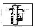
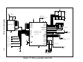
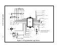
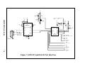
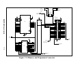
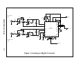
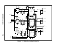
DSP56007EVM 24-BIT DIGITAL SIGNAL PROCESSOR EVALUATION MODULE USER’S GUIDE Motorola, Inc. Semiconductor Products Sector DSP Division 6501 William Cannon Drive, West Austin, Texas 78735-8598 CONTENTS INTRODUCTION . . . . . . . . . . . . . . . . . . . . . . . . . . . . . . . . . . . . . . . . . . . . . . . . . . 1-1 EVALUATION MODULE DESCRIPTION AND FEATURES . . . . . . . . . . . . . . 1-1 EQUIPMENT . . . . . . . . . . . . . . . . . . . . . . . . . . . . . . . . . . . . . . . . . . . . . . . . . . . . . 2-1 WHAT YOU GET WITH THE EVALUATION MODULE . . . . . . . . . . . . . . . . . . 2-1 WHAT YOU NEED TO SUPPLY . . . . . . . . . . . . . . . . . . . . . . . . . . . . . . . . . . . 2-2 EVM THEORY OF OPERATION . . . . . . . . . . . . . . . . . . . . . . . . . . . . . . . . . . . . . . 3-1 INPUTS AND OUTPUTS . . . . . . . . . . . . . . . . . . . . . . . . . . . . . . . . . . . . . . . . . 3-1 OPERATING MODE SELECTION . . . . . . . . . . . . . . . . . . . . . . . . . . . . . . . . . . 3-4 BOOTSTRAP CONFIGURATION USING JP9. . . . . . . . . . . . . . . . . . . . . . . . . 3-4 ONCETM PORT . . . . . . . . . . . . . . . . . . . . . . . . . . . . . . . . . . . . . . . . . . . . . . . . 3-5 RS-232 CONNECTIONS AND JP1 . . . . . . . . . . . . . . . . . . . . . . . . . . . . . . . . . 3-6 OPERATING MODES AND SRAM REFRESH IN THE 56007 . . . . . . . . . . . . 3-6 EVALUATION MODULE PARTS LIST . . . . . . . . . . . . . . . . . . . . . . . . . . . . . . . 3-6 POWER SUPPLIES . . . . . . . . . . . . . . . . . . . . . . . . . . . . . . . . . . . . . . . . . . . . . 3-6 MEMORY . . . . . . . . . . . . . . . . . . . . . . . . . . . . . . . . . . . . . . . . . . . . . . . . . . . . . 3-7 DIGITAL SIGNAL PROCESSOR OPERATING FREQUENCY . . . . . . . . . . . . 3-8 EXTERNAL INTERRUPT REQUESTS . . . . . . . . . . . . . . . . . . . . . . . . . . . . . . 3-8 PERIPHERAL SPECIFICATIONS . . . . . . . . . . . . . . . . . . . . . . . . . . . . . . . . . . . . . 4-1 CS5390 STEREO ADC . . . . . . . . . . . . . . . . . . . . . . . . . . . . . . . . . . . . . . . . . . 4-2 CS4331 STEREO DAC . . . . . . . . . . . . . . . . . . . . . . . . . . . . . . . . . . . . . . . . . . 4-3 CS3310 STEREO DIGITAL VOLUME CONTROL . . . . . . . . . . . . . . . . . . . . . . 4-4 CS8412 DIGITAL AUDIO INTERFACE RECEIVER. . . . . . . . . . . . . . . . . . . . . 4-5 CS8402A DIGITAL AUDIO INTERFACE TRANSMITTER . . . . . . . . . . . . . . . . 4-6 STK10C68 CMOS 2K X 8 NVSRAM . . . . . . . . . . . . . . . . . . . . . . . . . . . . . . . . 4-7 SC937-02 AES/EBU TRANSFORMER . . . . . . . . . . . . . . . . . . . . . . . . . . . . . . 4-8 LCD PANEL . . . . . . . . . . . . . . . . . . . . . . . . . . . . . . . . . . . . . . . . . . . . . . . . . . . 4-8 WIRING FOR KEYPAD . . . . . . . . . . . . . . . . . . . . . . . . . . . . . . . . . . . . . . . . . 4-10 EPM7032 PLD EQUATIONS . . . . . . . . . . . . . . . . . . . . . . . . . . . . . . . . . . . . . . . . . 5-1 INTRODUCTION TO THE GUI . . . . . . . . . . . . . . . . . . . . . . . . . . . . . . . . . . . . . . . 6-1 STARTING THE GUI . . . . . . . . . . . . . . . . . . . . . . . . . . . . . . . . . . . . . . . . . . . . 6-1 THE GUI WINDOWS . . . . . . . . . . . . . . . . . . . . . . . . . . . . . . . . . . . . . . . . . . . . 6-2 EVALUATION MODULE SCHEMATICS. . . . . . . . . . . . . . . . . . . . . . . . . . . . . . . . 7-1 SCHEMATIC DIAGRAMS . . . . . . . . . . . . . . . . . . . . . . . . . . . . . . . . . . . . . . . . 7-1 EVALUATION MODULE PARTS LIST . . . . . . . . . . . . . . . . . . . . . . . . . . . . . . . . . 8-1 PARTS LISTING. . . . . . . . . . . . . . . . . . . . . . . . . . . . . . . . . . . . . . . . . . . . . . . . 8-1 56007EVM User’s Guide iii -iv 56007EVM User’s Guide List Of Figures Figure 2-1 Figure 3-1 Figure 4-1 Figure 4-2 Figure 4-3 Figure 4-4 Figure 4-5 Figure 4-6 Figure 4-7 Figure 4-8 Figure 4-9 Figure 4-10 Figure 4-11 Figure 6-1 Figure 7-1 Figure 7-2 Figure 7-3 Figure 7-4 Figure 7-5 Figure 7-6 Figure 7-7 Figure 7-8 Figure 7-9 EVM Component Layout. . . . . . . . . . . . . . . . . . . . . . . . . . 2-2 JP9 Pinout . . . . . . . . . . . . . . . . . . . . . . . . . . . . . . . . . . . . 3-5 CS5390 ADC . . . . . . . . . . . . . . . . . . . . . . . . . . . . . . . . . . 4-2 CS4331 DAC . . . . . . . . . . . . . . . . . . . . . . . . . . . . . . . . . . 4-3 CS3310 Stereo Digital Volume Control . . . . . . . . . . . . . . 4-4 Serial Port Timing for the CS3310 . . . . . . . . . . . . . . . . . . 4-4 CS8412 Digital Audio Interface Receiver . . . . . . . . . . . . . 4-5 CS8402 Digital Audio Interface Transmitter . . . . . . . . . . . 4-6 STK10C68 8K x 8 nvSRAM . . . . . . . . . . . . . . . . . . . . . . . 4-7 SC937-02 AES/EBU Transformer . . . . . . . . . . . . . . . . . . 4-8 LCD Softswitch Screens . . . . . . . . . . . . . . . . . . . . . . . . . . 4-9 LCD Keypad Screens . . . . . . . . . . . . . . . . . . . . . . . . . . . 4-10 Keypad Wiring Diagram . . . . . . . . . . . . . . . . . . . . . . . . . 4-11 The GUI . . . . . . . . . . . . . . . . . . . . . . . . . . . . . . . . . . . . . . 6-2 DSP56007 . . . . . . . . . . . . . . . . . . . . . . . . . . . . . . . . . . . . 7-3 Microcontroller and LCD . . . . . . . . . . . . . . . . . . . . . . . . . 7-4 Programmable Logic Device . . . . . . . . . . . . . . . . . . . . . . 7-5 RS-232 and OnCE Port Interface . . . . . . . . . . . . . . . . . . 7-6 Memory and Expansion Connector . . . . . . . . . . . . . . . . 7-7 Analog-to-Digital Converter . . . . . . . . . . . . . . . . . . . . . . . 7-8 Digital-to-Analog Converter . . . . . . . . . . . . . . . . . . . . . . . 7-9 SPDIF I/O . . . . . . . . . . . . . . . . . . . . . . . . . . . . . . . . . . . 7-10 Power Supply . . . . . . . . . . . . . . . . . . . . . . . . . . . . . . . . . 7-11 List of Tables Digital Audio Input Selection . . . . . . . . . . . . . . . . . . . . . . . . . . . . . . . . . . . . . . . . . Digital Audio Receive/Transmit Jumper Configuration . . . . . . . . . . . . . . . . . . . . . Mode Select Jumpers . . . . . . . . . . . . . . . . . . . . . . . . . . . . . . . . . . . . . . . . . . . . . JP9 Configuration ............................................. DSP56007 Internal Memory Configurations . . . . . . . . . . . . . . . . . . . . . . . . . . . . . Frequency Products ............................................. 56007EVM User’s Guide 3-2 3-2 3-4 3-5 3-7 3-8 -iv -v 56007EVM User’s Guide SECTION 1 INTRODUCTION This document describes the basic structure, theory, and operation of the DSP56007EVM Evaluation Module (Evaluation Module), the equipment required to use the Evaluation Module, and the specifications of the key components on the Evaluation Module. Code samples and self-test code are provided on the accompanying software diskette. Evaluation Module schematic diagrams and a parts list are included as well. 1.1 EVALUATION MODULE DESCRIPTION AND FEATURES The DSP56007EVM is a low-cost platform for multichannel digital audio applications design, prototyping, and development. The fully assembled and tested circuit board contains: • 24-bit DSP56007 Digital Signal Processor operating at 66 MHz • 8192 bytes of off-chip SRAM and 8192 bytes of nonvolatile RAM • Standard 30-pin SIMM slot for easy, inexpensive DRAM expansion • One 20-bit stereo analog-to-digital converter (ADC), three 18-bit stereo digitalto-analog converters (DACs) • Programmable analog-domain attenuators on the digital-to-analog outputs • RCA jacks for all analog audio input/output 56007EVM User’s Guide 1-1 Introduction Evaluation Module Description and Features • Optical and transformer-isolated electrical SPDIF/CP340 stereo digital audio inputs and outputs • 50-pin expansion connector to provide the capability for expansion and/or substitution of other input/output peripherals, as well as easy interprocessor communication between Motorola Evaluation Modules • Socketed MC68HC11E9 (52-pin CLCC microcontroller) to allow the user to substitute user-programmed microprocessor and prototype custom 68HC11 code (allows connection to MC68HC11 emulation systems) • 2 × 16 character liquid crystal display (LCD) and four softswitches for user interface • Connector provides capability to use optional standard 4 × 4 keypad matrix • MC68705K1 microcontroller performing RS-232-to-OnCETM port command conversions 1-2 56007EVM User’s Guide SECTION 2 EQUIPMENT The following section gives a brief summary of the equipment required to use the Evaluation Module, some of which is supplied with the Evaluation Module, and some of which will have to be supplied by the user. 2.1 WHAT YOU GET WITH THE EVALUATION MODULE • Evaluation Module board (See Figure 2-1) • 3.5” disk titled ‘Debug - Evaluation Module’ • 3.5” disk titled ‘Evaluation Module Software’ • Debug - Evaluation Module manual • DSP56000 Family Manual • DSP56007 User’s Manual • DSP56007 Data Sheet • DSP56007EVM User’s Guide (this document), including Evaluation Module Schematics • Additional relevant documentation may be included in the form of a READ.ME file on the Evaluation Module Software disk. 56007EVM User’s Guide 2-1 Equipment What you need to supply Analog Inputs Analog Outputs Left 3 CS3310 Right 3 Left 2 Right 2 CS4331 CS3310 Left 1 CS4331 Right 1 Right In CS3310 Left In CS4331 CS5390 Optical In JP5 CS8412 JP3 Optical Out JP7 J5 JP2 30-Pin SIMM Socket PLD CS8402A J3 J9 DSP 56007 JP4 SPDIF In Analog Power STK10C68 J18 SPDIF Out JP9 SC937-02 JP6 68HC11E9 68HC705K1 JP1 RS-232 OnCETM LCD Display Reset J1 J2 Digital Power Infrared Remote Receiver Figure 2-1 Evaluation Module Component Layout 2.2 WHAT YOU NEED TO SUPPLY • A PC (-386 or higher) with minimum 2 Mbytes of memory, a 3.5” floppy disk drive, and a serial port capable of at least 19,200 bits-per-second data transfer rate. • An RS-232 cable (DB9 male to DB9 female) • Power supplies: dual 8-12V DC (for analog circuits), 8-15V AC or DC (for digital circuits) 2-2 56007EVM User’s Guide Equipment What you need to supply • An audio source, an audio amplifier driving headphones or speakers, and cables with RCA/phono connectors are required to use the demo software 56007EVM User’s Guide 2-3 Equipment What you need to supply 2-4 56007EVM User’s Guide SECTION 3 EVALUATION MODULE THEORY OF OPERATION Refer to Section 7, 56007EVM Schematics, for reference to pinouts and jumper configurations. 3.1 INPUTS AND OUTPUTS Analog signals connected to the Evaluation Module inputs are converted to 20 bitdata at the ADC. U19 and U20 attenuate the signal and convert it to balanced mode. The ADC has the Select Serial I/O Mode (SMODE) pin pulled high to make the ADC the SAI receive clock master. In master mode, the ADC’s Serial Data Clock (SCLK) and Left/Right Select (L/R) word clock pins are outputs. The L/R word clock output is the opposite polarity of I2S. It is inverted in the programmable logic device (PLD) to create true I2S. The ADC receives its oversampling clock on the Digital Section Clock Input (ICLKD), which is then internally divided by two, and this signal is provided to the Analog Section Clock Input (ICLKA). ICLKD can be driven from the 11.2896 MHz clock, the 12.288 MHz clock, or the 256 × Fs clock produced by the CS8412 AES/EBU Receiver. The Audio Power Down Input (APD) and Digital Power Down Input (DPD) pins are wired to the Cntl_Mute signal of the PLD. When pulled high, the ADC will be muted. When first pulled low, the ADC will be reset, then it will be enabled. 56007EVM User’s Guide 3-1 Evaluation Module Theory of Operation Inputs and Outputs The other possible input source comes from the SPDIF inputs (J14 for electrical input and J17 for optical input). Jumper JP4 selects the source (see Table 1 below). When receiving valid SPDIF input, the SPDIF Receiver drives the Master Clock (MCK) output that is 256 times the Frame Sync frequency of the received data. The CS8412 operates in Mode 3, the I2S slave mode. Table 3-1 Digital Audio Input Selection Selection 3.1.1 Jumper Settings Electric SPDIF JP4.1 to JP4.3 JP4.2 to JP4.4 Optical SPDIF JP4.3 to JP4.5 JP4.4 to JP4.6 Clock Select The Evaluation Module provides a means for the user to select which clock controls the reception and transmission of digital audio (see Table 3-2 below). JP2 selects the ADC and DAC clocks which, when jumpered, are set at 44.1 KHz and, when not jumpered, at 48 KHz. The expansion connector, J5, can be used to directly access the DSP. The receive SAI bus may be clocked by the selection made at JP2 (44.1 KHz or 48 KHz) or be clocked by the received SPDIF signal. The transmit SAI bus may be clocked by either the clock selected at JP2 or by the data and word clocks output from the DSP when it is in master mode. It is the user’s responsibility to ensure that data is output at the desired rate. See Table 3-2, below. Table 3-2 Digital Audio Receive/Transmit Jumper Configuration Receive/ Transmit 3-2 Jumper JP5.1 to JP5.2 Jumper JP5.3 to JP5.4 No Jumper Rx Clocked by crystal – Clocked by received SPDIF Tx – Clocked by crystal Clocked by DSP 56007EVM User’s Guide Evaluation Module Theory of Operation Inputs and Outputs 3.1.2 Serial Audio Interface (SAI) The DSP56007 SAI transmitter drives the six analog outputs and the SPDIF output. I2S is the default mode for the DACs. The Master Clock (MCLK) rate for the DACs is 256 × Fs. The dual RC networks after the DACs serve as AC couplers for audio data and as low-pass filters to convert the delta-sigma digital output pulses to analog waveforms. The digitally controlled analog domain attenuators receive the audio data and attenuate or amplify the data as determined by the microcontroller. The attenuators receive the Serial Clock Input (SCLK), Serial Data Input (SDATAI), and the Chip Select/Latch (CS) from the microcontroller. 3.1.3 Sony-Philips Digital Interface Format (SPDIF) The SPDIF transmitter receives data from the DSP through the Serial Data Input (SDATA) using the Frame Sync (FSYNC) and the Serial Data Clock (SCK). The transmitter outputs SPDIF audio signals through J15 (electrical) and J16 (optical). Fs_sens from the clock select appears at the expansion connector in order to read the sampling rate with the DSP’s General Purpose I/O (GPIO1) at J5.41 and also at U21-2 to select the state of the ‘sample-rate’ bits transmitted within the channel status block. See the SPDIF specification for more information. The channel status bits and block sync signals (DRcv_Blk, DTrn_Blk, DRcv_CS, and DTrn_CS) are available at J5.43 to allow the DSP to read one of them as well. Isolation transformers are used on both input and output, although they are not strictly required for SPDIF, because this Evaluation Module is intended to be used as a development system. 3.1.4 Other Inputs and Outputs The infrared remote receiver connects directly to the MC68HC711E9 and receives its commands from an infrared remote (though not currently implemented, this feature is planned for a future software release). The clock master is derived from one of two sources: the 11.2896 MHz clock or the 12.288 MHz clock. The microcontroller also receives commands from either the soft switches (S1, S2, S3, or S4) or from the Keypad Expansion Port, J18. The current user screen or the results of these commands are then displayed by a modular LCD panel with a 2 × 16 character display. The 56007EVM User’s Guide 3-3 Evaluation Module Theory of Operation Operating Mode Selection microcontroller code is capable of driving larger LCD displays, but all user screens are designed for a 2 × 16 character display. The MC68HC711E9 communicates with the DSP via the Serial Host Interface (SHI) port in SPI mode. When SS is pulled low, the microcontroller can write to the DSP. The MOSI and MISO lines pass control data through the DSP SHI in 24-bit mode. SCK is the SPI Shift Clock from the DSP. Again, the expansion connector, J5, can be used to access or intercept host port communications. The Control_Data, Control_Clock, and Control_Latch lines from the microcontroller control the digitally controlled analog domain attenuators. The Control_Mute line mutes the ADC and the DACs; low is muted, high is enabled. 3.2 OPERATING MODE SELECTION DSP56007EVM modes can be selected at JP3 as shown in Table 3-3. Once the mode has been selected, the PLD can receive interrupts from the network attached to J19. Table 3-3 Mode Select Jumpers Mode JP3.5 to JP3.6 JP3.3 to JP3.4 JP3.1 to JP3.2 0 X X X 1 X X - 2 X - X 3 X - - 4 - X X 5 - X - 6 - - X 7 - - - X = jumper installed; - = no jumper 3.3 BOOTSTRAP CONFIGURATION USING JP9 In the SHI bootstrap mode, JP9 can be configured to bootstrap the DSP by setting the jumpers according toTable 3-4. The first code-set contains the pass-through code included on the 56007EVM software disk. The second code-set currently contains shell 3-4 56007EVM User’s Guide Evaluation Module Theory of Operation OnCETM Port code to be replaced by Dolby ProLogic code in a future software release. JP9’s pinout is shown in Figure 3-1. Table 3-4 JP9 Configuration JP3.1 to JP3.4 Do not send bootstrap code from HC11 to DSP JP3.4 to JP3.1 Send bootstrap code from HC11 to DSP JP3.2 to JP3.5 Send 1st code-set in higher memory JP3.3 to JP3.6 Send peripheral changes as if running ProLogic/THX out of ROM JP3.5 to JP3.1 Send 2nd code-set in higher memory JP3.6 to JP3.1 Do not send peripheral changes 7 8 9 4 5 6 1 2 3 Figure 3-1 JP9 Pinout 3.4 ONCETM PORT The OnCETM port interface operates by receiving the serial data from the RS-232 Transceiver and executing commands sent by the host computer. These commands can reset the DSP, put the DSP in debug mode, release the DSP from debug mode, read and write to the OnCETM port, and read and write to the DSP itself. The serial bit rate is 19,200 bits/second. The RS-232 serial communications are performed in software on the MC68705K1. Port A of the MC68705K1 communicates with the DSP, and port B communicates with the host computer. The acknowledge signal from the OnCETM port is a low-going pulse on DS0. Since the 68705K1 is too slow to reliably catch this very narrow pulse, the pulse is latched in the PLD and the output of the latch appears on the ACK pin (PA2). When this occurs, the 68705K1 illuminates red LED D5 to indicate that the DSP is in the debug mode. For more information on the OnCETM port, see the DSP56000 Family Manual. The reset switch will reset the microcontroller, 56007EVM User’s Guide 3-5 Evaluation Module Theory of Operation RS-232 Connections and JP1 which will subsequently reset the DSP56007. The MC68705K1 source and object code are available from the Motorola DSP Division; contact your local Motorola FAE. 3.5 RS-232 CONNECTIONS AND JP1 RS-232 is an often-abused standard, and the direction of the signals present on pins 2 and 3 of the DB9 connectordo not always conform to the standard. JP1 provides the user with the ability to reverse these two pin connections without resorting to NULL Modem adapters or rewiring cable connectors. As shipped, JP1.1 is connected via shorting jumpers to JP1.3 and JP1.2 is connected to JP1.4. This connects J4.2 to the OUTPUT of the Evaluation Module’s RS-232 level converter (U4) and J4.3 to the INPUT of the board’s RS-232 receiver. These directions can be reversed by reorienting the shorting jumpers and turning them 90 degrees (one-quarter turn), thereby connecting JP1.1 to JP1.2 and JP1.3 to JP1.4. The user should never need to rewire an RS-232 connector in order to establish Evaluation Module communications with a host computer. 3.6 OPERATING MODES AND SRAM REFRESH IN THE 56007 In modes 0, 1, 2, and 3 the SRAM is refreshed from the nvRAM and the DSP can bootstrap from the SRAM via the EMI if a valid bootstrap mode is used. When in modes 4, 5, 6, and 7 the SRAM is not refreshed. Refreshes are not affected by jumpers on the expansion connector, J5. Jumpers J5.37 and J5.39 must be inserted to have full DSP control of the SRAM and nvRAM after bootstrap. 3.7 EVALUATION MODULE PARTS LIST The parts list of the DSP56007EVM is shown in Section 8. 3.8 POWER SUPPLIES The Evaluation Module requires power sources, for both analog and digital circuits, in order to operate. Bipolar analog power (use a linear power supply for best results) 3-6 56007EVM User’s Guide Evaluation Module Theory of Operation Memory is received through screw terminals at J3. Digital power is received through screw terminals at J2 or via a 2.1mm connector (J1). When the power is on, D6 (green LED) is illuminated. Analog power input may be 8 to 12 volts and digital power input may be 8 to 15 volts. While the voltage regulator can accommodate higher input voltage potentials, the added heat dissipation required at these input voltage levels will result in the regulator becoming dangerously warm and it is not recommended that the user subject the board to power inputs in excess of the maximum levels listed. Note: Always supply the Evaluation Module with analog power prior to or simultaneous with the application of digital power. If digital power is supplied before the analog power, the DACs may go into one of three possible error modes (no long-term damage to the device will occur) and will not function correctly. If analog power is supplied first, or if both analog power and digital power are applied simultaneously, these problems do not appear and the DACs are properly initialized. 3.9 MEMORY The Evaluation Module has 8K (8192) bytes each of fast Static RAM (SRAM) and of nonvolatile RAM (nvRAM). The SRAM operates at zero wait states at a 40 MHz DSP clock speed and with one wait state at 50 and 66 MHz. The contents of the SRAM may be block-loaded into nvRAM and the contents of the nvRAM may be block- loaded into the SRAM. The lowest 3072 bytes of the nvRAM may also be used to store code to load into the DSP via EMI bootstrap. On-chip DSP56007 memory includes: • 6348 × 24-bit on-chip program ROM and 52 × 24-bit bootstrap ROM • 1024 × 24-bit on-chip X-data RAM plus 512 × 24-bit on-chip X-data ROM • 2176 × 24-bit on-chip Y-data RAM plus 512 × 24-bit on-chip Y-data ROM • 1024 × 24- bits of the Y-data RAM can be configured as program RAM, replacing 1280 × 24 bits of program ROM Table 3-5 DSP56007 Internal Memory Configurations PE=0 PE=1 P_RAM 0 1.024K X_RAM 2.176K 1.024K 56007EVM User’s Guide 3-7 Evaluation Module Theory of Operation Digital Signal Processor Operating Frequency Table 3-5 DSP56007 Internal Memory Configurations (Continued) 3.10 PE=0 PE=1 Y_RAM 1.024K 1.152K P_ROM 6.348K 5.12K X_ROM 512 512 Y_ROM 512 512 DIGITAL SIGNAL PROCESSOR OPERATING FREQUENCY The DSP56007 is clocked at 768 kHz by a 12.288 MHz crystal divided by 16. The DSP56007 PLL is then used to multiply this frequency up to the desired operating frequency. Table 3-6 shows the frequency multiplication factors and the resulting DSP clock rates: Table 3-6 Frequency Products 2 1.536 MHz 16 12.288 MHz 30 23.040 MHz 44 33.792 MHz 58 44.544 MHz 72 55.296 MHz 3 2.304 MHz 17 13.056 MHz 31 23.808 MHz 45 34.560 MHz 59 45.312 MHz 73 56.064 MHz 4 3.072 MHz 18 13.824 MHz 32 24.576 MHz 46 35.328 MHz 60 46.080 MHz 74 56.832 MHz 5 3.840 MHz 19 14.592 MHz 33 25.344 MHz 47 36.096 MHz 61 46.848 MHz 75 57.600 MHz 6 4.608 MHz 20 15.360 MHz 34 26.112 MHz 48 36.864 MHz 62 47.616 MHz 76 58.368 MHz 7 5.376 MHz 21 16.128 MHz 35 26.880 MHz 49 37.632 MHz 63 48.384 MHz 77 59.136 MHz 8 6.144 MHz 22 16.896 MHz 36 27.648 MHz 50 38.400 MHz 64 49.152 MHz 78 59.904 MHz 9 6.912 MHz 23 17.664 MHz 37 28.416 MHz 51 39.168 MHz 65 49.920 MHz 79 60.672 MHz 10 7.680 MHz 24 18.432 MHz 38 29.184 MHz 52 39.936 MHz 66 50.688 MHz 80 61.440 MHz 11 8.448 MHz 25 19.200 MHz 39 29.952 MHz 53 40.704 MHz 67 51.456 MHz 81 62.208 MHz 12 9.216 MHz 26 19.968 MHz 40 30.720 MHz 54 41.472 MHz 68 52.224 MHz 82 62.976 MHz 13 9.984 MHz 27 20.736 MHz 41 31.488 MHz 55 42.240 MHz 69 52.992 MHz 83 63.744 MHz 14 10.752 MHz 28 21.504 MHz 42 32.256 MHz 56 43.008 MHz 70 53.760 MHz 84 64.512 MHz 15 11.520 MHz 29 22.272 MHz 43 33.024 MHz 57 43.776 MHz 71 54.528 MHz 85 65.280 MHz 3-8 56007EVM User’s Guide Evaluation Module Theory of Operation External Interrupt Requests 3.11 EXTERNAL INTERRUPT REQUESTS J19 allows the user to externally initiate the External Interrupt Request A (IRQA), the External Interrupt Request B (IRQB), and/or the Non-Maskable Interrupt Request (NMI). These pins are pulled high by 10k resistors to assure that false interrupts are not generated by floating inputs. 56007EVM User’s Guide 3-9 Evaluation Module Theory of Operation External Interrupt Requests 3-10 56007EVM User’s Guide SECTION 4 PERIPHERAL SPECIFICATIONS The following section describes the various peripheral devices used on the DSP56007EVM and includes any necessary equations and information. Contact information for the manufacturers of significant peripheral devices is included along with the parts listing in Section 8. 56007EVM User’s Guide 4-1 Peripheral Specifications CS5390 Stereo ADC 4.1 CS5390 STEREO ADC The CS5390 is a complete analog-to-digital converter (ADC) for stereo digital audio systems. It performs sampling, analog-to-digital conversion and anti-alias filtering, generating 20-bit values for both left and right inputs in serial form. The output word rate can be up to 50 kHz per channel. The CS5390 uses fifth-order, delta-sigma modulation with 64 times oversampling followed by digital filtering and decimation, which removes the need for an external anti-alias filter, beyond the simple balanced RC filter formed by R25, R26, and C8 (R31, R32, and C20 for the right channel). The ADC uses a differential architecture that provides excellent noise rejection. The CS5390 has a filter passband of DC to 21.7kHz. The filters are linear phase, have 0.005 dB passband ripple, and greater than 100 dB stopband rejection. The operating temperature range is 0o to 70o. ICLKA APD 28 27 VREF+ VREF- 4 + - 25 AGND ICLKD FSYNC SCLK L/R 19 + - LP Filter DAC 26 20 16 + - 13 15 11 12 Digital Decimation Filter Comparator Digital Decimation Filter + - LP Filter S/H DAC 23 VA+ 24 VA- Comparator Calibration Microcontroller 7 VL+ 6 LGND 9 10 DCAL DPD Figure 4-1 CS5390 ADC 4-2 14 Serial Output Interface S/H 1 OCLKD 5 Voltage Reference AINLAINL+ 3 AINRAINR+ ACAL 2 22 56007EVM User’s Guide Calibration SRAM 17 VD+ 18 DGND SDATA CMODE SMODE Peripheral Specifications CS4331 Stereo DAC 4.2 CS4331 STEREO DAC The CS4331 is a complete stereo digital-to-analog converter (DAC) with 18-bit resolution, including interpolation, 1-bit digital-to-analog conversion, and output analog filtering in an 8-pin package. The CS4331 is based on delta-sigma modulation where the modulator output controls the reference voltage input to an ultra-linear analog low-pass filter. This architecture allows for infinite adjustment of sample rate between 1 kHz and 50 kHz while maintaining linear phase response, simply by changing the master clock frequency. The CS4331 contains optional on-chip deemphasis and operates from a single +5V power supply. The CS4331 has a 96 dB dynamic range, less than 0.003% THD, low clock jitter sensitivity and completely filtered line level outputs that use linear-phase filtering. . DEM/SCLK/CONFIG 2 LRCK SDATAI AGND VA+ 6 7 3 1 Serial Input Interface De-emphasis Voltage Reference Interpolator Delta-Sigma Modulator DAC Analog Low-Pass Filter Interpolator Delta-Sigma Modulator DAC Analog Low-Pass Filter 8 5 AOUTL AOUTR 4 MCLK Figure 4-2 CS4331 DAC 56007EVM User’s Guide 4-3 Peripheral Specifications CS3310 Stereo Digital Volume Control 4.3 CS3310 STEREO DIGITAL VOLUME CONTROL The CS3310 is a complete stereo digital volume control designed specifically for audio systems. It features a 16-bit serial interface that controls two independent, low distortion (0.001% THD + N) audio channels. The CS3310 includes an array of well-matched resistors and a low-noise active output stage that is capable of driving a 600 Ω load. A total adjustable range of 127 dB, in 0.5 dB steps, is achieved through 95.5 dB of attenuation and 31.5 dB of gain. The simple 3-wire interface provides daisy-chaining of multiple CS3310s for multi-channel audio systems. The device operates from ±5V supplies and has an input/output voltage range of ±3.75V. AINL 16 14 + - M U X AOUTL 8 MUTE 8 8 AGNDL 15 AGNDR 10 8 M U X AINR 1 Control Register 8 2 16 Serial to Parallel Register + 9 12 13 3 7 6 ZCEN CS SDATAI SDATAO SCLK AOUTR 4 5 VA+ VA- VD+ DGND Figure 4-3 CS3310 Stereo Digital Volume Control CS SCLK SDATAI R7 R6 R5 R4 R3 R2 R1 R0 L7 L6 L5 L4 L3 L2 L1 L0 SDATAO R7 R6 R5 R4 R3 R2 R1 R0 L7 L6 L5 L4 L3 L2 L1 L0 L0 = Left Channel Least Significant Bit L7 = Left Channel Most Significant Bit R0 = Right Channel Least Significant Bit R7 = Right Channel Most Significant Bit SDATA is latched internally on the rising edge of SCLK SDATAO transitions after the falling edge of SCLK SDATAO bits reflect the data previously loaded into the CS3310 Figure 4-4 Serial Port Timing for the CS3310 4-4 56007EVM User’s Guide Peripheral Specifications CS8412 Digital Audio Interface Receiver 4.4 CS8412 DIGITAL AUDIO INTERFACE RECEIVER The CS8412 is a monolithic CMOS device that receives and decodes audio data according to the AES 3 - 1992, EBU Tech. 3250-E, IEC 958, SPDIF, and EIAJ CP-340 interface standards. The CS8412 receives data from a transmission line, recovers the clock and synchronization signals, and de-multiplexes the audio and non-audio data. Either differential or single-ended inputs can be decoded. The CS8412 de-multiplexes the channel, user, and validity data directly to dedicated output pins for the most commonly needed channel status bits. VD+ 7 9 RXP 10 RXN DGND VA+ 8 22 FILT AGND 20 21 Clock & Data Recovery RS-422 Receiver Mux 13 CS12/FCK 16 SEL 6 MCK 5 M3 M2 M1 M0 19 17 18 24 23 Audio Serial Port De-Mux Mux 4 Registers 3 2 1 CO/ Ca/ Cb/ Cc/ Cd/ Ca/ E0 E1 E2 F0 F1 F2 25 26 12 11 1 14 28 SDATA SCLK FSYNC C U VERF 15 ERF CBL Figure 4-5 CS8412 Digital Audio Interface Receiver 56007EVM User’s Guide 4-5 Peripheral Specifications CS8402A Digital Audio Interface Transmitter 4.5 CS8402A DIGITAL AUDIO INTERFACE TRANSMITTER The CS8402A is a monolithic CMOS device that encodes and transmits audio data according to the AES 3 - 1992, EBU Tech. 3250-E, IEC 958, SPDIF, and EIAJ CP-340 interface standards. The CS8402A accepts audio and non-audio data and multiplexes and encodes the data. The audio serial port is double-buffered and capable of supporting a wide variety of formats. The CS8402A multiplexes the channel, user, and validity data directly from dedicated input pins for the most commonly needed channel status bits. M2 M1 M0 23 22 21 6 SCK 7 FSYNC 8 SDATA C U V 10 11 9 MCK 5 RST 16 Audio Serial Port RS422 Driver MUX Registers 7 15 Dedicated Channel Status Bits 24 CBL TRNPT Figure 4-6 CS8402 Digital Audio Interface Transmitter 4-6 56007EVM User’s Guide 20 17 TXP TXN Peripheral Specifications STK10C68 CMOS 2K x 8 nvSRAM 4.6 STK10C68 CMOS 2K X 8 NVSRAM The Simtek STK10C68 is a fast static RAM (25, 30, 35, and 45ns), with a nonvolatile electrically-erasable PROM (EEPROM) element incorporated in each static memory cell. The SRAM can be read and written an unlimited number of times while independent, nonvolatile data resides in EEPROM. Data may easily be transferred from the SRAM to the EEPROM (STORE cycle), or from the EEPROM to the SRAM (RECALL cycle) using the NE pin (nonvolatile enable). It combines the high performance and ease of use of a fast SRAM with nonvolatile data integrity. The STK10C68 features 12, 15, 20, and 25ns output enable access times, hardware STORE and RECALL initiation, automatic STORE and RECALL timing, 104 or 105 STORE cycles to EEPROM, unlimited RECALL cycles from EEPROM, and 10-year data retention in EEPROM. The STK10C68 requires a single +5V power supply. Input Buffers A3 A4 A5 A6 A7 A8 A9 A12 EEPROM Array 256 × 256 Store Static RAM Recall Array 256 × 256 Input Buffers DQ0 DQ1 DQ2 DQ3 DQ4 DQ5 DQ6 DQ7 Column I/O Column Decoder Store/ Recall Control A0 A1 A2 A10 A11 G NE E W Figure 4-7 STK10C68 8K × 8 nvSRAM 56007EVM User’s Guide 4-7 Peripheral Specifications SC937-02 AES/EBU Transformer 4.7 SC937-02 AES/EBU TRANSFORMER The AES/EBU circuit incorporates a transformer to reject common mode interference while transmitting the signal with fast rise time and minimum aberration. The SC93702 is a surface mount, low capacitance, wide-band AES/EBU transformer. The SC93702 has a very low capacitance shielded winding that reduces both radiated and received noise coupling and provides decreased jitter and improved audio quality, especially in noisy environments. EMI compliance and EMI susceptibility are improved by the use of this type of transformer. The transformer’s ratio is 1:1, primary inductance is 600µH, inter-winding capacitance is 1.1pF, bandwidth is 16kHz to 100MHz, and rise-time is 3ns. Input Input Rtn 1 8 2 7 3 6 4 5 Output Rtn Output Figure 4-8 SC937-02 AES/EBU Transformer 4.8 LCD PANEL Figure 4-9 illustrates the different screens of the LCD panel and the corresponding actions of the soft switches. Note that ProLogic and THX functionality is not available on the generic DSP56007EVM. The attenuator trim functions (shown in the trim section in Figure 4-9) are fully functional on the generic 56007EVM. Figure 4-10 illustrates the different screens of the LCD with respect to the 4 × 4 keypad matrix. 4-8 56007EVM User’s Guide Peripheral Specifications LCD Panel Mode is Byp PL THX Set Mode is Bypass Byp PL Mode is Mode is THX Set Byp PL THX Set Byp Mode is PL THX Dolby 4-Ch Mode Mode is THX 3Ch Byp 4Ch Ext PL THX Set 4Ch Ext PL Mstr Vol Set Dolby 3-Ch Mode 3Ch Byp - + THX Set 0dB Nxt Ex Delay Time 20ns (Selecting THX sets decoding mode to Dolby 4-channel plus THX enhancements) - + Nxt Ex Center Mode Phn Nrm Wid Nxt Subwoofer is Off Off On Nxt Ex Trim Section (in the “Set” menu): Lft Trim - + LSur Trim - + 0dB Nxt Cntr Trim Ex 0dB Nxt Ex - 0dB + Nxt Sub Trim 0dB - + Nxt Rgt Trim Ex - + 0dB Nxt RSur Trim Ex - + 0dB Nxt Ex Ex Re-equalization (Dolby 4-channel mode and THX mode must be active): Re-EQ is Off Off On Nxt Re-EQ is On Ex On Nxt On Nxt Delay Time Re-EQ is Off Off Off Ex - + Re-EQ is ISO2969 Ex ISO Flat Acad Ex 20ms Nxt Ex Figure 4-9 LCD Softswitch Screens 56007EVM User’s Guide 4-9 Peripheral Specifications Wiring for Keypad Keypad 1 2 3 4 5 6 7 8 9 10 11 12 13 14 15 16 9 Test Tone On Left 1 DNE 2 Bypass 3 Prologic 3 Channel Mode Prologic 4 Channel Mode 10 Increment Test Tone Level 11 Increment Delay Time 4 Prologic THX 12 DNE 5 DNE 6 Subwoofer On Subwoofer Off 14 Decrement Test Tone Level 7 DNE 15 Decrement Delay Time 8 Center Mode Small Center Mode Large 16 DNE +06.0 Test Tone Off * 13 Test Tone On Left +06.0 Test Tone On Right +06.0 * If THX is selected, the Test Tone scr Left, Center, If Prologic 3 Left, Center, If Prologic 4 Left, Center, Center Mode None Right, R. Sur., L. Sur. Channel Mode is selecte Right, (Subwoofer). Channel Mode is selecte Right, R. Sur., L. Sur. Figure 4-10 LCD Keypad Screens 4.9 WIRING FOR KEYPAD A wiring diagram for a generic keypad is shown in Figure 4-11. 4-10 56007EVM User’s Guide Peripheral Specifications Wiring for Keypad 9 8 7 6 Button # 1 5 4 3 Button # 16 2 1 10 Figure 4-11 Keypad Wiring Diagram 56007EVM User’s Guide 4-11 Peripheral Specifications Wiring for Keypad 4-12 56007EVM User’s Guide EPM7032 PLD Equations SECTION 5 EPM7032 PLD EQUATIONS The following data represents the PLD equations for the DSP56007EVM: ACK_RST : INPUT; ClkSelA : INPUT; CLKSELB : INPUT; CNTL_MUTE : INPUT; DSO : INPUT; DSP_RST : INPUT; EMI_MRD : INPUT; EXP2_~WSR : INPUT; FS_SENS : INPUT; IRQA : INPUT; IRQB : INPUT; IRQC : INPUT; MODA_SEL : INPUT; MODB_SEL : INPUT; MODC_SEL : INPUT; RCVMASTER_SEL : INPUT; TXMASTER_SEL : INPUT; 11MHZ_CLK : INPUT; 12MHZ_CLK : INPUT; 8412_MCK : INPUT; % ACK = _LC031 % ACK = LCELL( _EQ001 $ _EQ001 = _X001; GND); 56007EVM User’s Guide 5-1 EPM7032 PLD Equations _X001 _X002 = EXP( DSO & _X002); = EXP( ACK_RST & _X001); % ADA_CLK = _LC006 % ADA_CLK = LCELL( _EQ002 $ GND); _EQ002 = FS_SENS & _LC026 # !FS_SENS & _LC025; % ADA_Clk/2 = _LC019 % % ADA_Clk/2 = |74393:15|Q1A % ADA_Clk/2 = TFFE( VCC, _EQ003, VCC, _EQ003 = _X003 & _X004; _X003 = EXP(!FS_SENS & _LC025); _X004 = EXP( FS_SENS & _LC026); % DSP_CLK = _LC020 % % DSP_CLK = |74393m:82|QD % DSP_CLK = TFFE( _EQ004, !_LC026, VCC, _EQ004 = _LC009 & _LC013 & _LC027; VCC, VCC, % DSP_MODA = _LC010 % DSP_MODA = LCELL( _EQ005 $ GND); _EQ005 = DSP_RST & IRQA # !DSP_RST & MODA_SEL; % DSP_MODB = _LC011 % DSP_MODB = LCELL( _EQ006 $ GND); _EQ006 = DSP_RST & IRQB # !DSP_RST & MODB_SEL; % DSP_MODC = _LC012 % DSP_MODC = LCELL( _EQ007 $ GND); _EQ007 = DSP_RST & IRQC # !DSP_RST & MODC_SEL; % EXP2_GPIO2 = _LC016 % EXP2_GPIO2 = TRI(_LC016, GLOBAL(!DSP_RST)); _LC016 = LCELL( GND $ GND); % EXP2_GPIO3 = _LC021 % EXP2_GPIO3 = TRI(_LC021, GLOBAL(!DSP_RST)); _LC021 = LCELL( GND $ GND); 5-2 56007EVM User’s Guide VCC); VCC); EPM7032 PLD Equations % EXP2_SCKT = |74393:15|Q1B % EXP2_SCKT = TRI(_LC002, GLOBAL(!TXMASTER_SEL)); _LC002 = TFFE( ADA_Clk/2, _EQ008, VCC, VCC, _EQ008 = _X003 & _X004; % EXP2_WSR = _LC003 % EXP2_WSR = LCELL(!EXP2_~WSR $ VCC); GND); % EXP2_WST = |74393:15|Q2D % EXP2_WST = TRI(_LC017, GLOBAL(!TXMASTER_SEL)); _LC017 = TFFE( _EQ009, !_LC015, VCC, VCC, VCC); _EQ009 = _LC004 & _LC014 & _LC024; % NVRAM_G = _LC001 % NVRAM_G = LCELL( _EQ010 $ GND); _EQ010 = DSP_RST & EMI_MRD # !DSP_RST & MODC_SEL; % 5390_CLK = _LC023 % 5390_CLK = LCELL( _EQ011 $ GND); _EQ011 = FS_SENS & _LC026 & !RCVMASTER_SEL # !FS_SENS & _LC025 & !RCVMASTER_SEL # RCVMASTER_SEL & 8412_MCK; % |clockpr4:111|:26 % _LC026 = TFFE( VCC, 12MHZ_CLK, VCC, VCC, VCC); % |clockpr4:111|:28 % _LC025 = TFFE( VCC, 11MHZ_CLK, VCC, VCC, VCC); VCC, VCC, VCC); VCC, VCC, _LC007; VCC); % |74393:15|Q1C = |74393:15|:5 % _LC007 = TFFE( _EQ012, _EQ013, _EQ012 = ADA_Clk/2 & _LC002; _EQ013 = _X003 & _X004; % |74393:15|Q1D = |74393:15|:9 % _LC015 = TFFE( _EQ014, _EQ015, _EQ014 = ADA_Clk/2 & _LC002 & _EQ015 = _X003 & _X004; % |74393:15|Q2A = |74393:15|:28 % _LC004 = TFFE( VCC, !_LC015, VCC, VCC, 56007EVM User’s Guide VCC); 5-3 EPM7032 PLD Equations % |74393:15|Q2B = |74393:15|:29 % _LC014 = TFFE( _LC004, !_LC015, % |74393:15|Q2C = |74393:15|:30 % _LC024 = TFFE( _EQ016, !_LC015, _EQ016 = _LC004 & _LC014; VCC, VCC, VCC); VCC, VCC, VCC); % |74393m:82|QA = |74393m:82|:1 % _LC009 = TFFE( VCC, !_LC026, VCC, % |74393m:82|QB = |74393m:82|:3 % _LC013 = TFFE( _LC009, !_LC026, % |74393m:82|QC = |74393m:82|:5 % _LC027 = TFFE( _EQ017, !_LC026, _EQ017 = _LC009 & _LC013; % ~CNTL_MUTE = _LC029 % ~CNTL_MUTE = LCELL(!CNTL_MUTE $ 5-4 VCC, VCC); VCC, VCC, VCC); VCC, VCC, VCC); GND) 56007EVM User’s Guide Introduction to the GUI Starting the GUI SECTION 6 INTRODUCTION TO THE GUI This section will give an introduction to the Graphical User Interface (GUI), detailing only that which is required to work through the brief example below. Full details of the GUI can be found in the Debug - Evaluation Module manual. 6.1 STARTING THE GUI To start up the GUI, type ‘evm56K’. The display you see will be similar to that shown in Figure 6-1. 56007EVM User’s Guide 6-1 Introduction to the GUI The GUI Windows DATA HEX REGISTERS HEX UNASSEMBLE COMMAND MENU Figure 6-1 The GUI 6.2 THE GUI WINDOWS The DATA window, shown in the top left corner, displays the data. To display the contents of X data memory, starting at location x:0, position the pointing device cursor in the COMMAND window, click once, and type: display x:0. The radix in which the data is shown can be changed by clicking in the box that contains the word HEX in the diagram above. Data can also be displayed in a graphical form. To do this type: display x:0 -graph. To change back to text type: display x:0 -text. The UNASSEMBLE window shows an unassembled version of the contents of program memory. The next instruction to be executed will be highlighted. The COMMAND window is where OnCE commands (i.e., the controlling commands) are entered. The REGISTERS window shows the contents of the registers of the ALU (Arithmetic Logic Unit) and the AGU (Address Generation Unit) 6-2 56007EVM User’s Guide +5V 53 28 9 52 29 10 DSP_RST 3-B4, 2-G3, 4-F3 56007EVM User’s Guide 36 37 38 39 DSP_MODA 3-B3 DSP_MODB 3-B3 DSP56007 EXTAL QVCC2 QVCC1 QVCC0 QGND2 QGND1 QGND0 PVCC PCAP PINIT PGND RESET MODA/IRQA MODB/IRQB MODC/NMI +5V 70 DSP_MODC 3-B3 MRD 77 78 2 79 80 3 MRAS MCAS EMI 3-F3, 5-A4 7-3 MA13 MA12 MA11 MA10 MA9 MA8 MA7 MA6 MA5 MA4 MA3 MA2 MA1 MA0 4 5 7 11 12 13 14 16 18 19 20 22 23 24 25 MD7 MD6 MD5 MD4 MD3 MD2 MD1 MD0 62 63 64 65 67 68 69 71 27 33 32 30 31 61 DR DSO 58 DSI/OS0 59 DSCK/OS1 60 +5V /DR 4-F4 DSO 4-F4, 3-F4 DSI/OS0 4-F5 DSCK/OS1 4-F5 SGND2 54 SGND1 44 SGND0 34 MRD MWR MCS0 MA17/ MCS1 MA16/ MCS2 MA15/ MCS3 MA14 MA13 MA12 MA11 MA10 MA9 MA8 MA7 MA6 MA5 MA4 MA3 MA2 MA1 MA0 MD7 MD6 MD5 MD4 MD3 MD2 MD1 MD0 45 46 47 49 50 SDO2 SDO1 SDO0 SCKT WST 56 SDI1 SDI0 57 SCKR 51 WSR 55 SDI1 SDI0 SCKR WSR SDO2 SDO1 SDO0 SCKT WST GPIO3 GPIO2 GPIO1 GPIO0 7 68 kHz C1 0.01 µF 48 SVCC1 40 SVCC0 DVCC0 72 DGND1 66 DGND0 MWR DSP_Clk 3-F2 +5V EXP1 5-G4 +5V R6 10 K GPIO3 GPIO2 GPIO1 GPIO0 73 74 75 76 D_HREQ D_SCK D_MISO D_SS D_MOSI HREQ 43 SCK/SCL 26 35 MISO/SDA 42 SS/HA2 41 MOSI/HA0 +5V 17 AVCC1 6 AVCC0 1 AGND0 8 AGND1 15 AGND2 21 AGND3 Figure 7-1 DSP56007 OnCE Int er f ace +5V R10 10 K R20 20 K Contrast 3 1 +5V 56007EVM User’s Guide U16 LCD Panel Vss 1 HC11_Clk 4-F2 +5V 3 Vo DB7 DB6 DB5 DB4 DB3 DB2 DB1 DB0 R12 10 K R13 10 K S3 S4 4 MHz Cl ock 2 2 Vdd R11 10 K 14 13 12 11 10 9 8 7 E 6 R/W 54 RS PC7 PC6 PC5 PC4 PC3 PC2 PC1 PC0 E R/W RS PC7 PC6 PC5 PC4 PC3 PC2 PC1 PC0 16 15 14 13 12 11 10 9 RS R/W E 35 36 37 38 39 40 41 42 6 Cntl_Data 7-A6 52 Cntl_Clk 7-A6 +5V Cntl_Latch 7-A6 26 Vdd 7 EXTAL PC7/A7/D7 PC6/A6/D6 PC5/A5/D5 PC4/A4/D4 PC3/A3/D3 PC2/A2/D2 PC1/A1/D1 PC0/A0/D0 PB7/A15 PB6/A14 PB5/A13 PB4/A12 PB3/A11 PB2/A10 PB1/A9 PB0/A8 U2 MC68HC711E9 Microcontroller STRB/R/ W 4 1 3 5 7 9 34 33 32 31 30 29 28 27 J18 Keypad expansion +5V PD5/SS PD4/SCK PD3/MOSI PD2/MISO PD1/TxD PD0/RxD 25 24 23 22 21 20 PE7/AN7 PE3/AN3 PE6/AN6 PE2/AN2 PE5/AN5 PE1/AN1 PE4/AN4 PE0/AN4 50 49 48 47 46 45 44 43 R3 1 0 K D_SS D_SCK D_MOSI D_MISO 2 JP8 1 2-pin male header +5V 7-4 1 2 3 DSP_RST 1-E3, 3-B4, 4-F3 EXP2 7-A3, 3-F3, 5-E4, 8-G2, 6-G3, 8-B4 R8 10 K 2 4 6 8 10 XIRQ 1817 RESET 19 IRQ VRH 51 VRL Vss 1 HC11_GPIO 5-F5 S2 5 E STRA/AS PA0/IC3 PA1/IC2 PA2/IC1 PA3/IC4/OC5/OC1 PA4/OC4/OC1 PA5/OC3/OC1 PA6/OC2/OC1 PA7/PAI/OC1 2 MODB/VSTBY 3 MODA/LIR Cntl_Mute 7-G4, 3-D4, 8-B5 8 XTAL S1 4 5 6 7 8 9 JP9 Configuration Jumpers Figure 7-2 Microcontroller and LCD IR_Rcv 3-B4 +5V R14 10 KΩ R9 10 KΩ R15 10 KΩ R5 10 KΩ NVRAM_G 5-D6 R4 R2 10 KΩ 10 KΩ ADA_Clk 7-A2 56007EVM User’s Guide 4 3 2 1 J19 Interrupts ADA_Clk/2 8-C3 +5V 2 4 6 DSP_Clk 1-H3 1 3 5 JP 3 Mode Select 1 5 6 37 2 7 8 10 11 12 40 14 13 18 19 20 21 22 DSP_MODA 1-E3 DSP_MODB 1-E4 DSP_MODC 1-E4 DSP_RST 1-E3, 2-G3, 4-F3 +5V 17 9 29 41 Vcc Vcc Vcc Vcc U5 EPM7032 PLD Gnd Gnd Gnd Gnd 24 4 36 16 42 3 33 32 15 35 43 44 23 31 34 38 30 28 27 26 25 39 EXP2 7-A3, 5-E4, 2-F4, 8-G2, 6-G3, 8-B4 GPIO2 WST SCKT WSR ~WSR GPIO3 EMI 5-A4, 1-F5 ~MRD 8412_MCK 8-G1 5390_Clk 6-G2 DSO 1-I4, 4-F4 +5V 2 IR Rcv. U22 Infared Receiver 3 1 IR_Rcv 2-F4 Cntl_Mute 7-G4, 2-B4, 8-B5 ~Cntl_Mute 6-F4 +5V +5V Y1 11.2896 MHz Oscillator 1 2 3 R1 ACK_RST 4-F4 10 KΩ 1 1 2 3 7-5 Y2 12.288 MHz Oscillator JP 2 2 Clock Select (7 6 8 kHz ) R57 10 KΩ R48 10 KΩ Tx 1 3 2 4 JP5 Master Select Rx Rx - Jumper- C locked by cry s t a l No Jumper-Cl ocked by Rcvd SPDIF Tx - Jumper- C locked by cry s t a l No Jumper-Cl ocked by DSP ACK 4-F4 Fs_sens 5-D2, 8-B5 Jumpe r - 11.2 8 96 MHz No Jumper- 12.2 8 8 MHz Figure 7-3 Programmable Logic Device +5V D7 1N5827 56007EVM User’s Guide C22 1 µF MAX232 5 C2C1RS-232 Transceiver 11 T1out T1in 7 10 T2out T2in 6 2 7 1 3 2 4 1 3 R1in 3 8 4 9 5 J4 OnCE/Host R1out 1 2 8 R2in JP1 Serial Config Reset R2out 9 V6 C3 47 pF C2 47 pF +5V C2+ 4 U4 14 1 S5 16 Vcc 2 V+ 1 C1+ 3 HC11_Clk 2-D2 +5V C4 1 µF C5 1 µF R17 10 KΩ Gnd 15 Y3 4 MHz C6 1 µF R16 1500 Ω MC68705K1 1 2 3 4 5 6 7 8 U24 OSC1 RST OSC2 PB1 Vss PB0 IRQ/Vpp Vdd PA7 PA0 PA1 PA6 PA2 PA5 PA3 PA4 OnCE Controller C7 1 µF D5 Debug LED Red 16 15 14 13 12 11 10 9 DSP_RST 1-E3, 3-B4, 2-G3 /DR 1-I3 ACK_RST 3-D5 DSO 1-I4, 3-F4 ACK 3-D5 DSCK/OS1 1-I4 7-6 DSI/OS0 1-I4 Figure 7-4 RS-232 and OnCE Port Interface DRcv_Blk 8-G3 DRcv_CS 8-G3 DTrn_CS 8-B5 DTrn_Blk 8-B5 JP7 NAD Select 6 5 4 3 2 1 Fs_sens 3-D6, 8-B5 30-Pin SIMM Socket MWR 21 56007EVM User’s Guide MCAS 2 MRAS 27 Vcc W Vcc CAS 24 19 18 17 15 14 12 11 8 7 5 4 DQ7 DQ6 DQ5 DQ4 DQ3 DQ2 DQ1 DQ0 A11 A10 A9 A8 A7 A6 A5 A4 A3 A2 A1 A0 J5 Expansion Connector +5V 30 RAS U15 MA11 MA10 MA9 MA8 MA7 MA6 MA5 MA4 MA3 MA2 MA1 MA0 +5V 1 25 23 20 16 13 10 6 3 MD7 MD6 MD5 MD4 MD3 MD2 MD1 MD0 R19 R45 10 K 10 K GPIO3 GPIO2 Q8 26 28 SDO2 SDO1 SDO0 SCKT WST CAS8 D8 Vss 22 D_MOSI D_MISO D_SS D_SCK 29 Vss 9 SDI1 SDI0 SCKR WSR EMI 3-F3, 1-F5 49 47 45 43 41 39 37 35 33 31 29 27 25 23 21 19 17 15 13 11 9 7 5 3 1 +5V 50 48 46 44 42 40 38 36 34 32 30 28 26 24 22 20 18 16 14 12 10 8 6 4 2 +5V STK10C48 7-7 MA12 MA7 MA6 MA5 MA4 MA3 MA2 MA1 MA0 MD0 MD1 MD2 1 2 3 4 5 6 7 8 9 10 11 12 13 14 NE nc A7 A6 A5 A4 A3 A2 A1 A0 D0 D1 D2 Vss U6 Vcc WE nc A8 A9 nc G A10 E D7 D6 D5 D4 D3 SRAM/nvRAM MWR MA13 MA8 MA9 MA11 7-A3, 3-F3, 2-F4, 8-G2, 6-G3, 8-B4 HC11_GPIO 2-B4 MA10 MD7 MD6 MD5 MD4 MD3 NVRAM_G 3-F2 Figure 7-5 Memory and Expansion Connector D_HREQ D_MOSI D_MISO D_SS D_SCK SDO2 SDO1 SDO0 SCKT WST SDI1 SDI0 SCKR WSR EXP1 1-I4 EXP2 28 27 26 25 24 23 22 21 20 19 18 17 16 15 GPIO0 GPIO1 GPIO2 GPIO3 +AVcc R47 Lef t Anal og R22 I nput 20 K R24 10 K 2 1 3 56007EVM User’s Guide R21 20 K 3 2 5 AGND AGND AGND R25 39.2 6 1 U19 U19 7 R26 39.2 AGND C8 6.8 nF NPO R29 10 K 2 1 3 U20 2 AGND U7 CS5390 5 AGND AGND 0.22 µF 7 R32 39.2 C11 100 µF 12 OCLKD 20 CMODE 11 A/D Converter 28 VREF+ DCAL 9 ACAL 5 27 VREF- TST02 21 8 TST01 C12 6 U20 17 VD+ 16 FSYNC SDATA 15 14 SCLK 13 L/ R 26 AINR+ C20 6.8 nF NPO 10 K 1 3-F4 SMODE R31 39.2 R30 19 ICLKD VA+ 3 AINL+ 25 AINR3 23 7 4 AINL- 2 R27 20 K J7 22 ICLKA VL+ R28 20 K 1 +5V 0.01 µF R23 10 K 2 1 J6 5390_Clk 51 C63 C21 100 µF VA- AGND APD 24 1 2 DPD 10 LGND DGND 18 6 -AVss Ri ght A nal og I nput AGND AGND AGND ~Cntl_Mute 3-D5 7-8 Figure 7-6 Analog-to-Digital Converter SDI0 SCKR WSR EXP2 7-A3, 3-F3, 5-E4, 2-F4, 8-G2, 8-B4 +AVcc +AVcc U9 R50 CS4331 D/A Converter 7 VA+ 1 2 3 SDATAI C45 0.1 µF 10 4 MCLK AOUTL 8 DEM/SCLK AOUTR 5 C72 3.3 µF C73 3.3 µF LRCK AGND 6 R53 56 K 4 R39 AGND 600 16 7 C15 C16 .0027 µF 3 56007EVM User’s Guide 6 2 AGND 2 AOUTR 11 2 SDATAI ZCEN SCLK MUTE 1 8 CS AGND AGNDL AGNDR VA- DGND 15 10 13 5 AGND -AVss +AVcc D/A Converter SDO2 SDO1 SDO0 SCKT WST 7 VA+ 1 2 SDATAI AOUTL 8 DEM/SCLK AOUTR 3 LRCK EXP2 5 AGND 6 3-F3, 5-E4, 2-F4, 8-F1, C74 3.3 µF R41 C75 3.3 µF R42 R55 56 K 6-G3, 8-A4 600 4 VD+ 16 12 VA+ AINL AOUTL 14 9 AINR R56 56 K 2 3 SDATAI ZCEN 6 SCLK MUTE 2 CS AGND 7 VA+ 1 2 3 SDATAI AOUTL 8 DEM/SCLK AOUTR 5 C28 3.3 µF C66 3.3 µF LRCK AGND 6 R51 56 K 7-9 Cntl_Clk 2-B4 Cntl_Mute 2-B4, 3-D4, 8-B5 -AVss +AVcc Left Output 1 R37 2 4 AGND 16 AOUTL CS3310 9 AINR 2 AOUTR 11 Dig Vol Cntrl C14 .0027 µF 7 3 6 SDATA0 SDATAI ZCEN SCLK MUTE 2 CS AGND J9 Right Output 1 1 14 U11 600 C13 .0027 µF VA+ AINL R38 R52 56 K 12 VD+ 600 1 8 AGNDL AGNDR VA- DGND 15 10 13 5 Cntl_Latch 2-B4 J8 1 0.1 µF AGND Cntl_Data 2-B3 AGND C44 CS4331 D/A Converter 4 MCLK 1 8 AGNDL AGNDR VA- DGND 10 5 15 13 AGND U8 J11 Right Output 2 1 AOUTR 11 CS3310 Dig Vol Cntrl 7 SDATA0 C18 .0027 µF AGND +AVcc Left Output 2 2 U13 600 C17 .0027 µF J10 1 AGND 4 MCLK J13 Right Output 3 1 SDATA0 0.1 µF CS4331 14 Dig Vol Cntrl C46 U10 +AVcc U12 CS3310 9 AINR R54 56 K .0027 µF Left Output 3 AINL AOUTL 600 J12 1 VA+ R40 AGND ADA_Clk 3-F2 12 VD+ AGND -AVss Figure 7-7 Digital-to-Analog Converter AGND +AVcc +5V C26 0.1 µF J14 CP340 In 1 L4 SC937-02 1 22 VA+ C65 0.1 µF 5 MCK 9 R7 75 2 4 8 2 4 6 2 C68 0.1 µF +5V 2 JP4 10 1 3 5 13 25 Input Select 1 27 1 56007EVM User’s Guide 2 3 J17 Optical In 256Fs 7 VD+ 3 2 4 Fibre Optic Receiver 5 6 20 RXP VERF RXN SCK SDATA CS12/FCK ERF CE/F2 U23 FSYNC CS8412 SEL 28 12 SCKR 26 SDI1 11 WSR 17 CD/F1 M2 18 CC/F0 M1 24 M0 23 CB/E2 CA/E1 C C0/E0 FILT C27 0.047 µF R46 1 K U AGND 21 DGND 8 CBL +5V WST 7 1 DRcv_CS 5-F1 14 15 DRcv_Blk 5-D1 AGND SCKT 6 SDO0 8 9 EXP2 7-A3, 3-F3, 5-E4, 2-F4, 8-F1, 6-G3 R49 10 K DTrn_CS 5-F2 DTrn_Blk 5-D2 7-10 Fs_sens 3-D6, 5-D2 Cntl_Mute 7-G4, 2-B4, 3-D4 5 MCK 19 VD+ C67 0.1 µF SCK TXP SDATA CS8402A V TXN C/SBF 11 U 15 CBL/SBC M2 M1 C7/ C3 4 C6/ C2 3 M0 PRO C1/FC0 16 RST EM0/ C9 12 C9/ C15 EM1/ C8 24 R44 90.9 17 L3 SC937-02 8 1 J15 CP340 Out 1 2 5 4 6 +5V AES/EBU Transmitter 1 R43 374 20 U21 10 +5V AGND FSYNC 23 +5V 22 2 21 Mode 4 2 14 13 TRNPT/FC1 GND 18 Figure 7-8 SPDIF I/O 1 J16 Optical Out 3 Fibre Optic Transmitter +5V Mode 3 128Fs ADA_Clk/2 3-F2 EXP2 7-A3, 3-F3, 5-E4, 2-F4, 6-G3, 8-A4 16 M3 AES/EBU Receiver 8412_MCK 3-F4 19 Di gi t al d ecoup l i ng Caps — al l 0 .1 µ F unl es s ot her w i se no ted C29 - C37 - U1 C4 2- U6 C38 - U2 C4 3- U7 C39 - U4 C4 7- U2 1 C40 ,C4 1 - U5 C4 8- U2 3 J2 U14 Power Input Terminal Block +5V MC7805 D1 Voltage Regulator 1N5827 1 56007EVM User’s Guide J1 D2 5-20 V AC/DC 1N5827 IN OUT 3 GROUND Ferrite C29 C30 C31 C32 C33 C34 C35 C36 C37 C38 C39 C40 C41 C42 C43 C47 C48 R18 2 Power Input L1 1500 C10 D4 1N5827 D3 C19 C9 1N5827 100 µF 1 µF 1 µF D6 Power Green U17 MC7805 Voltage Regulator 1 +AVcc C49 C51 C52 C53 C54 VOUT 3 VIN C56 C58 C60 C61 C62 C69 C70 C71 GND 2 C64 C24 100 µF 1 µF JP6 1 J3 Analog Power 2 1 Ground Connect 2 3 Connector C23 AGND DGnd C25 100 µF 1 1 µF GND 2 VIN VOUT 3 C50 U18 MC7905 C55 C57 C59 -AVss Voltage Regulator Anal og De coupl i ng Caps — al l 0 .1 µ F 7-11 unl e ss ot her w i se no te d C4 9 ,C5 0- U7 C56 ,C57 ,C7 0 - U1 2 C5 1 - U8 C58 ,C59 ,C7 1 - U1 3 C5 2 - U9 C60 - U1 9 C5 3 - U10 C61 - U2 0 C5 4 ,C5 5,C6 9- U1 1 C62 - U2 3 Figure 7-9 Power Supply Evaluation Module Parts List Parts Listing SECTION 8 EVALUATION MODULE PARTS LIST 8.1 PARTS LISTING The following four pages contain, in table form, information on the parts and devices on the Evaluation Module. Contact information for suppliers of key devices, as indicated by footnote, is also included at the end of the table. 56007EVM User’s Guide 8-1 Evaluation Module Parts List Parts Listing Table 8-1 DSP56007EVM Parts List Part Designator Manufacturer Part Number Description U1 Motorola DSP56007 DSP U2 Motorola MC68HC711E9 Microcontroller U24 Motorola MC68HC705K1 Microcontroller (OnCE) U7 Crystal a CS5390-KS ADC U8 U9 U10 Crystal a CS4331-KS DAC U21 Crystal a CS8402-CS AES/EBU Transmitter U23 Crystal a CS8412-CS AES/EBU Receiver U11 U12 U13 Crystal a CS3310-KS Digital Volume Controller L3 L4 Scientific Conversion SC937-02 Audio Isolation Transformer b U6 Simtek c STK1068-S45 SRAM/nVRAM U16 Hitachi LM052L LCD Module U14 U17 Motorola MC7805 Voltage Regulator U18 Motorola MC7905 Voltage Regulator U19 U20 Motorola MC33078 Op-Amp U5 Altera EPM7032TC44-12 PLD D1 D2 D3 D4 D7 Rectron FM4001 Rectifier, SMD U4 Maxim MAX232CSE RS232 Transceiver C4 C5 C6 C7 C9 C10 C22 C24 C25 Murata GRM42-6Y5V105Z16BL 1.0µF capacitor C28 C66 C72 C73 C74 C75 TDK CC1206CY5V335ZTR 3.3 µF capacitor C1 C63 Murata GRM42-6XR103K050BD 0.01µF capacitor C8 C20 Venkel C1210C0G500-682JNE 6.8nF capacitor C11 C19 C21 C23 C64 Future SME25T101M6X16LL 100µF Aluminum Electrolytic capacitor 8-2 56007EVM User’s Guide Evaluation Module Parts List Parts Listing Table 8-1 DSP56007EVM Parts List (Continued) Part Designator Manufacturer Part Number Description C2 C3 Murata GRM426C0G470J050BD 47pF capacitor C26 C29 C30 C31 C33 C34 C35 C36 C37 C38 C39 C40 C41 C42 C43 C44 C45 C46 C47 C48 C49 C50 C51 C52 C53 C54 C55 C56 C57 C58 C59 C60 C61 C62 C65 C67 C68 C69 C70 C71 Murata GRM426X7R104K050BL 0.1µF capacitor C27 Venkel C1206X7R500-473KNE 0.047µF capacitor C13 C14 C15 C16 C17 C18 Venkel C1206X7R500-272KNE 0.0027µF capacitor C12 Venkel C1206X7R500-224KNE 0.22µF capacitor 10Ω 1/4W resistor R50 R25 R26 R31 R32 Venkel CR1206-8W-39R2FT 39.2Ω 1/4W resistor R47 Venkel CR1206-8W-51R1FT 51Ω 1/4W resistor 75Ω 1/4W resistor R7 R44 Venkel CR1206-8W-90R9FT 90.9Ω 1/4W resistor R43 Venkel CR1206-8W-3740FT 374Ω 1/4W resistor R37 R38 R39 R40 R41 R42 Future NRC12F604OTR 604Ω 1/4W resistor R46 Future CRCW1206-102JRT1 1.0KΩ 1/4W resistor R16 R18 Newark 44F6300-1.5K 1.5KΩ 1/4W resistor R1 R2 R3 R4 R5 R6 R8 R9 R10 R11 R12 R13 R14 R15 R17 R19 R23 R24 R29 R30 R45 R48 R49 R57 Future CR32-1002F-T 10KΩ 1/4W resistor R21 R27 20kΩ 1/4W resistors R51 R52 R53 R54 R55 R56 56KΩ 1/4W resistors 56007EVM User’s Guide 8-3 Evaluation Module Parts List Parts Listing Table 8-1 DSP56007EVM Parts List (Continued) Part Designator Manufacturer Part Number Description R20 R22 R28 Digikey D4AA24-ND 20KΩ 1/4W trimpot thruhole Y1 MMD MB100HA-11.2896MHz 11.2896MHz Clock Oscillator Y2 MMD MB100HA-12.288MHz 12.288MHz Clock Oscillator Y3 Ecliptek EC2-040-4.000MHz-I 4.0MHz Crystal JP2 JP6 JP8 2-pin single row header J19 4-pin single row header JP1 JP5 4-pin double row header JP3 JP4 JP7 6-pin double row header J18 10-pin double row header on PC board for U16 14-pin single row female header on PC board for U16 14-pin single row male header J5 50-pin double row male header on PC board for U15 SIMM socket J17 Sharp GP1F32R Optical Connector-Receive J16 Sharp GP1F32T Optical Connector-Transmit J1 Mouser 16PJ031 2.1mm DIN power connector J4 Mouser 152-3409 PC mount DB9 female connector J7 J9 J11 J13 J6 J8 J10 J13 J14 J15 Mouser 161-4215 RCA Jack on PC board for U2 McKensie PLCC-52P-T 52-pin PLCC socket J2 2-position terminal block J3 3-position terminal block S1 S2 S3 S4 S5 6mm pushbutton switch 8-4 56007EVM User’s Guide Evaluation Module Parts List Parts Listing Table 8-1 DSP56007EVM Parts List (Continued) Part Designator Manufacturer Part Number Description D6 Future HLMP1790 Green LED 2mA, 1.8V D5 Future HLMP1700 Red LED 2mA, 1.8V U22 Sharp GP1U56Y Infrared receiver L1 Future BL01RN1-A62 Ferrite on PC board for U14 TO-220 0.5” compact heat sink a.Crystal Semiconductor Corporation, P.O. Box 17847, Austin, TX 78760, (512) 445-7222 Fax: b.Scientific Conversion, Inc., 42 Truman Drive, Novato, CA 94947,(415) 892-2323, Fax: (415) c.Simtek Corporation, 1465 Kelly Johnson Blvd., Colorado Springs, CO 80920, (800) 637-1667, 9481 56007EVM User’s Guide 8-5 Evaluation Module Parts List Parts Listing 8-6 56007EVM User’s Guide Index 11.2896 MHz clock . . . . . . . . . . . . . 3-3 12.288 MHz clock . . . . . . . . . . . . . 3-3 12.288 MHz crystal . . . . . . . . . . . . 3-8 DSP56000 Family Manual . . . . . . DSP56007 . . . . . . . . . . . . . . . . . . . . DSP56007 Data Sheet . . . . . . . . . . DSP56007 memory . . . . . . . . . . . . . DSP56007 User’s Manual . . . . . . . A E ACK . . . . . . . . . . . . . . . . . . . . . . . . . 3-5 ADC . . . . . . . . . . . . . . . . . . . . . 3-1, 4-2 AES/EBU Transformer . . . . . . . . 4-8 analog-to-digital conversion . . . . 4-2 Analog-to-Digital Converter . . . . 7-8 anti-alias filtering . . . . . . . . . . . . . 4-2 attenuator trim functions . . . . . . . 4-9 Audio Power Down Input (APD) 3-1 electrically-erasable PROM (EEPROM) . . . . . . . . . . . . . . . . . . . 4-7 EMI bootstrap . . . . . . . . . . . . . . . . . 3-7 EMI susceptibility . . . . . . . . . . . . . 4-8 EPM7032 . . . . . . . . . . . . . . . . . . . . . 5-1 Expansion Connector, J5 . . . . . . . . . . . . . . . . . . . . . 3-2, 3-4, 7-7 External Interrupt Requests . . . . . 3-8 B F Bipolar analog power . . . . . . . . . . 3-6 Bootstrap Configuration . . . . . . . 3-4 fast static RAM . . . . . . . . . . . . . . . fast Static RAM (SRAM) . . . . . . . . Frame Sync (FSYNC) . . . . . . . . . . frequency multiplication factors . Numerics C Chip Select/Latch (CS) . . . . . . . . . Clock Select . . . . . . . . . . . . . . . . . . Control_Mute . . . . . . . . . . . . . . . . . CS3310 . . . . . . . . . . . . . . . . . . . . . . . CS4331 . . . . . . . . . . . . . . . . . . . . . . . CS5390 . . . . . . . . . . . . . . . . . . . . . . . CS8402A . . . . . . . . . . . . . . . . . . . . . CS8412 . . . . . . . . . . . . . . . . . . . . . . . 3-3 3-2 3-4 4-4 4-3 4-2 4-6 4-5 D DB9 connector . . . . . . . . . . . . . . . . 3-6 debug mode . . . . . . . . . . . . . . . . . . 3-5 Digital Audio Interface Receiver . . . . . . . . . . . . . . . . . . . . . 4-5 Digital Audio Interface Transmitter . . . . . . . . . . . . . . . . . . . 4-6 Digital power . . . . . . . . . . . . . . . . . 3-6 Digital Power Down Input (DPD) 3-1 digital-to-analog conversion . . . . 4-3 Digital-to-Analog Converter . . . . 7-9 Dolby ProLogic. . . . . . . . . . . . . . . . 3-5 2-1 7-3 2-1 3-7 2-1 4-7 3-7 3-3 3-8 G Graphical User Interface (GUI) . . 6-1 GUI Windows . . . . . . . . . . . . . . . . 6-2 I I2S . . . . . . . . . . . . . . . . . . . . . . . . . . I2S slave mode . . . . . . . . . . . . . . . . ICLKA . . . . . . . . . . . . . . . . . . . . . . . ICLKD . . . . . . . . . . . . . . . . . . . . . . . 3-1 3-2 3-1 3-1 J Jumper JP4 . . . . . . . . . . . . . . . . . . . 3-1 K keypad . . . . . . . . . . . . . . . . . . . . . 4-12 Keypad Expansion Port,J18 . . . . . 3-3 L LCD . . . . . . . . . . . . . . . . . . . . . . . . . 7-4 56007EVM User’s Guide I-i Index LCD panel . . . . . . . . . . . . . . . .3-3, 4-9 M Master Clock (MCLK) . . . . . . . . . 3-3 master mode . . . . . . . . . . . . . . . . . 3-1 MC68705K1 . . . . . . . . . . . . . . . . . . 3-5 MC68HC711E9 . . . . . . . . . . . . . . . 3-3 Memory . . . . . . . . . . . . . . . . . .3-7, 7-7 Microcontroller . . . . . . . . . . . . . . . 7-4 MISO . . . . . . . . . . . . . . . . . . . . . . . . 3-4 MOSI . . . . . . . . . . . . . . . . . . . . . . . . 3-4 N Non-Maskable Interrupt Request (NMI) . . . . . . . . . . . . . . . . 3-8 nonvolatile RAM (nvRAM) . . . . . 3-7 O OnCETM Port . . . . . . . . . . . . . .3-5, 7-6 Operating Frequency . . . . . . . . . . 3-8 Operating Mode Selection . . . . . . 3-4 output analog filtering . . . . . . . . . 4-3 sample rate . . . . . . . . . . . . . . . . . . . 4-3 SC937-02 . . . . . . . . . . . . . . . . . . . . . 4-8 schematic diagrams . . . . . . . . . . . 7-1 Serial Clock Input (SCLK) . . . . . . 3-3 Serial Data Clock (SCK) . . . . . . . . 3-3 Serial Data Input (SDATA) . . . . . 3-3 Serial Data Input (SDATAI) . . . . . 3-3 Serial Host Interface (SHI) port . . 3-4 SHI bootstrap mode . . . . . . . . . . . 3-4 soft switches . . . . . . . . . . . . . . .3-3, 4-9 SPDIF . . . . . . . . . . . . 3-1, 3-3, 4-5, 4-6 SPDIF I/O . . . . . . . . . . . . . . . . . . 7-10 SPDIF output . . . . . . . . . . . . . . . . . 3-3 SPDIF transmitter . . . . . . . . . . . . . 3-3 SPI mode . . . . . . . . . . . . . . . . . . . . . 3-4 SRAM refresh . . . . . . . . . . . . . . . . . 3-6 Stereo ADC . . . . . . . . . . . . . . . . . . . 4-2 Stereo DAC . . . . . . . . . . . . . . . . . . 4-3 Stereo Digital Volume Control . . 4-4 STK10C68 . . . . . . . . . . . . . . . . . . . . 4-7 STORE cycle . . . . . . . . . . . . . . . . . . 4-7 T THX . . . . . . . . . . . . . . . . . . . . . . . . . 4-9 transmit SAI bus . . . . . . . . . . . . . . 3-2 P PLD . . . . . . . . . . . . . . 3-1, 3-4, 3-5, 5-1 PLD Equations . . . . . . . . . . . . . . . . 5-1 PLL . . . . . . . . . . . . . . . . . . . . . . . . . 3-8 Power supplies . . . . . . . 2-2, 3-6, 7-11 Programmable Logic Device . . . . 7-5 ProLogic . . . . . . . . . . . . . . . . . . . . . 4-9 W wait states . . . . . . . . . . . . . . . . . . . . 3-7 R RECALL cycle . . . . . . . . . . . . . . . . RS-232 . . . . . . . . . . . . . . . . . . . . . . . RS-232 and OnCE Port Interface . RS-232 cable . . . . . . . . . . . . . . . . . . RS-232 serial communications . . . RS-232 Transceiver . . . . . . . . . . . . 4-7 3-6 7-6 2-2 3-5 3-5 S SAI transmitter . . . . . . . . . . . . . . . 3-3 56007EVM User’s Guide I-ii Motorola reserves the right to make changes without further notice to any products herein. Motorola makes no warranty, representation or guarantee regarding the suitability of its products for any particular purpose, nor does Motorola assume any liability arising out of the application or use of any product or circuit, and specifically disclaims any and all liability, including without limitation consequential or incidental damages. “Typical” parameters can and do vary in different applications. All operating parameters, including “Typicals” must be validated for each customer application by customer’s technical experts. Motorola does not convey any license under its patent rights nor the rights of others. Motorola products are not designed, intended, or authorized for use as components in systems intended for surgical implant into the body, or other applications intended to support or sustain life, or for any other application in which the failure of the Motorola product could create a situation where personal injury or death may occur. Should Buyer purchase or use Motorola products for any such unintended or unauthorized application, Buyer shall indemnify and hold Motorola and its officers, employees, subsidiaries, affiliates, and distributors harmless against all claims, costs, damages, and expenses, and reasonable attorney fees arising out of, directly or indirectly, any claim of personal injury or death associated with such unintended or unauthorized use, even if such claim alleges that Motorola was negligent regarding the design or manufacture of the part. Motorola and B are registered trademarks of Motorola, Inc. Motorola, Inc. is an Equal Opportunity/ Affirmative Action Employer. OnCE and Symphony are trade marks of Motorola, Inc. Motorola Inc., 1995