1
Freescale
Users Guide
KQRUG
Rev. 2, 08/2012
Kinetis Peripheral Module
Quick Reference
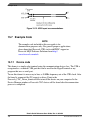
A Compilation of Demonstration Software for Kinetis Modules
This collection of code examples, useful tips, and quick
reference material has been created to help you speed the
development of your applications. Most chapters in this
document contain examples that can be modified to work
with Kinetis MCU Family members. When you are
developing your application, consult your device data
sheet and reference manual for part-specific information,
such as which features are supported on your device.
Sample code can be found at KINETIS512_SC.zip,
available from http://freescale.com
Information about the ARM core can be found in the help
center at http://ARM.com
The most up-to-date revisions of our documents are on
the Web. Your printed copy may be an earlier revision.
To verify that you have the latest information available,
refer to http://freescale.com
© Freescale 2012. All rights reserved.
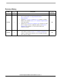
Revision History
Date
Revision
Level
11/2010
0
03/2012
Initial release
N/A
•
Added two new chapters, Chapter 8: Using the Flash Software
Drivers, and Chapter 20: Using OPAMP for Kinetis
Microcontrollers.
•
Updated Fig. 13-3, Fig. 13-4 and Fig. 13-5 of Chapter 13: ENET
Module. Also updated Section 13.5.1.1: Hardware Implementation,
of the same chapter.
Added a note to Section 14.4: Example Code, of Chapter 14: USB
Device Charger Detection (USBDCD) Module, and Section 15.7:
Example Code, of Chapter 15: Universal Serial Bus OTG
(USBOTG) Module.
1
•
•
08/2012
Page
Number(s)
Description
2
•
Deleted the sentence “Refer to the full source code for this example
in the ZIP file” from the Section 7.1.5.2: Module configuration, of
Chapter 7: Enhanced Direct Memory Access (eDMA) Controller
N/A
N/A
Minor editorial changes
Kinetis Peripheral Module Quick Reference, Rev. 2
2
Freescale Semiconductor
Contents
Section number
Title
Page
Chapter 1
General System Setup (Software Considerations)
1.1
Software considerations..................................................................................................................................................15
1.1.1
Overview............................................................................................................................................................15
1.1.2
Code execution...................................................................................................................................................15
1.1.3
Reset and booting...............................................................................................................................................15
1.1.4
1.1.3.1
Device state during reset....................................................................................................................16
1.1.3.2
Device state after reset.......................................................................................................................16
Typical system initialization .............................................................................................................................16
1.1.4.1
Lowest level assembly routines.........................................................................................................16
1.1.4.1.1
Initialize general purpose registers.................................................................................16
1.1.4.1.1.1 Unmask interrupts at ARM core ................................................................17
1.1.4.1.1.2 Branch to start of C initialization code.......................................................17
1.1.4.2
Startup routines..................................................................................................................................17
1.1.4.2.1
Disable watchdog............................................................................................................17
1.1.4.2.2
Initialize RAM................................................................................................................17
1.1.4.2.3
Enable port clocks...........................................................................................................18
1.1.4.2.4
Ramp system clock to selected frequency......................................................................18
1.1.4.2.5
Enable pin interrupt.........................................................................................................18
1.1.4.2.6
Enable UART for terminal communication....................................................................18
1.1.4.2.7
Jump to start of main function for application................................................................19
Chapter 2
General System Setup (Hardware Considerations)
2.1
Hardware considerations.................................................................................................................................................21
2.1.1
Overview............................................................................................................................................................21
2.1.2
Floorplan............................................................................................................................................................21
2.1.2.1
Connectors.........................................................................................................................................22
2.1.2.2
Power domains...................................................................................................................................22
Kinetis Quick Reference User Guide, Rev. 2, 08/2012
Freescale Semiconductor, Inc.
3
Section number
2.1.3
Title
Page
PCB routing considerations...............................................................................................................................23
2.1.3.1
Power supply routing.........................................................................................................................23
2.1.3.2
Power supply decoupling and filtering..............................................................................................24
2.1.3.3
Oscillators..........................................................................................................................................25
2.1.3.4
2.1.3.3.1
RTC oscillator.................................................................................................................26
2.1.3.3.2
MCG oscillator................................................................................................................26
General filtering.................................................................................................................................29
2.1.3.4.1
RESET_b and NMI_b.....................................................................................................29
2.1.3.4.2
General purpose I/O........................................................................................................30
2.1.3.4.3
Analog inputs..................................................................................................................30
2.1.4
PCB layer stack-up.............................................................................................................................................30
2.1.5
Other module hardware considerations..............................................................................................................33
2.1.5.1
VBAT.................................................................................................................................................33
2.1.5.2
Voltage reference module..................................................................................................................34
2.1.5.3
Debug interface..................................................................................................................................34
Chapter 3
Nested Vector Interrupt Controller (NVIC)
3.1
NVIC...............................................................................................................................................................................37
3.1.1
3.1.2
Overview............................................................................................................................................................37
3.1.1.1
Introduction .......................................................................................................................................37
3.1.1.2
Features .............................................................................................................................................37
Configuration examples.....................................................................................................................................38
3.1.2.1
Configuring the NVIC.......................................................................................................................38
3.1.2.1.1
3.1.2.2
Relocating the vector table.................................................................................................................39
3.1.2.2.1
3.1.2.3
Code example and explanation.......................................................................................38
Code example and explanation.......................................................................................40
Disabling priorities.............................................................................................................................40
3.1.2.3.1
Code example and explanation.......................................................................................41
Kinetis Quick Reference User Guide, Rev. 2, 08/2012
4
Freescale Semiconductor, Inc.
Section number
Title
Page
Chapter 4
Clocking System
4.1
Clocking..........................................................................................................................................................................43
4.1.1
Overview............................................................................................................................................................43
4.1.2
Features..............................................................................................................................................................43
4.1.3
Configuration examples.....................................................................................................................................45
4.1.3.1
Transitioning to PLL engaged external mode....................................................................................46
4.1.3.1.1
4.1.3.2
Transitioning between PLL engaged external mode and bypassed low power internal mode..........47
4.1.3.2.1
4.1.3.3
Code example and explanation.......................................................................................46
Code example and explanation.......................................................................................47
Configuring the FLL with the RTC oscillator as a reference............................................................48
4.1.3.3.1
Code example and explanation.......................................................................................48
4.1.4
Clocking system device hardware implementation...........................................................................................49
4.1.5
Layout guidelines for general routing and placement........................................................................................50
4.1.6
References..........................................................................................................................................................50
Chapter 5
Power Management Controller (PMC/MODECTL)
5.1
Using the power management controller........................................................................................................................51
5.1.1
Overview............................................................................................................................................................51
5.1.1.1
5.1.2
5.2
Introduction........................................................................................................................................51
Using the low voltage detection system.............................................................................................................51
5.1.2.1
Features..............................................................................................................................................51
5.1.2.2
Configuration examples.....................................................................................................................52
5.1.2.3
Interrupt code example and explanation............................................................................................53
5.1.2.4
Hardware implementation..................................................................................................................53
Using the mode controller...............................................................................................................................................54
5.2.1
Overview............................................................................................................................................................54
5.2.1.1
Introduction........................................................................................................................................54
5.2.1.2
Features..............................................................................................................................................55
Kinetis Quick Reference User Guide, Rev. 2, 08/2012
Freescale Semiconductor, Inc.
5
Section number
5.2.2
5.3
Title
Page
Configuration examples.....................................................................................................................................55
5.2.2.1
MC code example and explanation....................................................................................................56
5.2.2.2
Entering low leakage stop (LLS) mode.............................................................................................56
5.2.2.3
Entering wait mode............................................................................................................................57
5.2.2.4
Exiting low power modes..................................................................................................................57
Using the low leakage wakeup unit................................................................................................................................58
5.3.1
5.3.2
Overview............................................................................................................................................................58
5.3.1.1
Mode transitions ................................................................................................................................58
5.3.1.2
Wakeup sources ................................................................................................................................58
Configuration examples.....................................................................................................................................58
5.3.2.1
Module wakeup..................................................................................................................................58
5.3.2.2
Pin wakeup.........................................................................................................................................59
5.3.2.3
LLWU port and module interrupts.....................................................................................................59
5.3.2.4
Wakeup sequence...............................................................................................................................60
5.4
Module operation in low power modes..........................................................................................................................61
5.5
Mode transition requirements.........................................................................................................................................62
5.6
Source of wakeup, pins and modules..............................................................................................................................64
Chapter 6
Memory Protection Unit (MPU)
6.1
Using the memory protection unit module.....................................................................................................................65
6.1.1
Overview............................................................................................................................................................65
6.1.2
Introduction........................................................................................................................................................65
6.1.3
Features..............................................................................................................................................................65
6.1.4
Configuration examples.....................................................................................................................................66
6.1.4.1
Region descriptors setup....................................................................................................................66
Kinetis Quick Reference User Guide, Rev. 2, 08/2012
6
Freescale Semiconductor, Inc.
Section number
Title
Page
Chapter 7
Enhanced Direct Memory Access (eDMA) Controller
7.1
eDMA.............................................................................................................................................................................67
7.1.1
Overview............................................................................................................................................................67
7.1.1.1
7.1.2
Introduction .......................................................................................................................................67
eDMA trigger.....................................................................................................................................................69
7.1.2.1
DMA multiplexer...............................................................................................................................69
7.1.2.2
Trigger mode......................................................................................................................................70
7.1.2.3
Multiple transfer requests...................................................................................................................71
7.1.3
Transfer process—major and minor transfer loop.............................................................................................72
7.1.4
Configuration steps ...........................................................................................................................................73
7.1.5
Example—PIT-gated DMA requests ................................................................................................................73
7.1.5.1
Requirements.....................................................................................................................................73
7.1.5.2
Module configuration.........................................................................................................................74
Chapter 8
Using the Flash Standard Software Drivers
8.1
Overview.........................................................................................................................................................................77
8.2
Downloading flash software drivers...............................................................................................................................77
8.3
Features...........................................................................................................................................................................78
8.4
Configuration parameters................................................................................................................................................78
8.4.1
SSD configuration structure...............................................................................................................................78
8.4.2
SSD derivative...................................................................................................................................................79
8.5
Demo code......................................................................................................................................................................79
8.6
Additional resources.......................................................................................................................................................82
Chapter 9
Using the FlexMemory
9.1
Using the FlexNVM .......................................................................................................................................................83
9.1.1
Overview............................................................................................................................................................83
9.1.1.1
Introduction .......................................................................................................................................83
9.1.1.2
Features..............................................................................................................................................83
Kinetis Quick Reference User Guide, Rev. 2, 08/2012
Freescale Semiconductor, Inc.
7
Section number
9.1.2
Title
Configuration examples ....................................................................................................................................84
9.1.2.1
Basic data flash..................................................................................................................................84
9.1.2.1.1
9.1.2.2
9.1.2.3
Code example and explanation.......................................................................................84
EEPROM flash records......................................................................................................................84
9.1.2.2.1
Code Example and Explanation......................................................................................85
Combination.......................................................................................................................................85
9.1.2.3.1
9.1.3
Page
Code example and explanation.......................................................................................86
Endurance...........................................................................................................................................................86
Chapter 10
EzPort Module
10.1 Using the EzPort module ...............................................................................................................................................89
10.1.1 Overview............................................................................................................................................................89
10.1.1.1 Introduction .......................................................................................................................................89
10.1.1.2 Features .............................................................................................................................................89
10.1.1.3 Command description........................................................................................................................90
10.1.1.3.1 Command format............................................................................................................90
10.1.1.3.2 Command timing............................................................................................................91
10.1.1.4 Status register.....................................................................................................................................92
10.1.2 Configuration examples ....................................................................................................................................92
10.1.2.1 Hardware connections........................................................................................................................92
10.1.2.2 Write enable and disable....................................................................................................................94
10.1.2.3 Sector erase and program...................................................................................................................94
10.1.2.4 Write and read FCCOB registers.......................................................................................................95
10.1.2.5 Write and read FlexRAM...................................................................................................................96
Chapter 11
Flexbus Module
11.1 Using the Flexbus module .............................................................................................................................................97
11.1.1 Overview............................................................................................................................................................97
11.1.1.1 Introduction........................................................................................................................................97
Kinetis Quick Reference User Guide, Rev. 2, 08/2012
8
Freescale Semiconductor, Inc.
Section number
Title
Page
11.1.1.2 Features .............................................................................................................................................97
11.1.1.2.1 Signal descriptions..........................................................................................................97
11.1.1.2.2 Address and data bus multiplexing ................................................................................98
11.1.1.2.3 Modes of Operation........................................................................................................99
11.1.1.2.4 Burst cycles.....................................................................................................................100
11.1.1.2.5 Data Byte Alignment and Physical Connections ...........................................................100
11.1.1.2.6 Memory map...................................................................................................................101
11.1.1.2.7 Reference clock...............................................................................................................101
11.1.1.3 Configuration examples ....................................................................................................................102
11.1.1.3.1 Code example and explanation.......................................................................................102
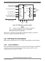
11.1.1.4 Hardware implementation..................................................................................................................103
11.1.2 PCB design recommendations...........................................................................................................................104
11.1.2.1 Layout guidelines...............................................................................................................................104
Chapter 12
Universal Asynchronous Receiver and Transmitter (UART) Module
12.1 Overview.........................................................................................................................................................................105
12.2 Features...........................................................................................................................................................................105
12.3 Configuration example....................................................................................................................................................106
12.3.1 UART initialization example.............................................................................................................................106
12.3.2 UART receive example......................................................................................................................................107
12.3.3 UART transmit example....................................................................................................................................108
12.3.4 UART configuration for interrupts or DMA requests.......................................................................................108
12.4 UART RS-232 hardware implementation......................................................................................................................109
Chapter 13
ENET Module
13.1 Overview.........................................................................................................................................................................111
13.1.1 Introduction........................................................................................................................................................111
13.1.2 Features..............................................................................................................................................................112
Kinetis Quick Reference User Guide, Rev. 2, 08/2012
Freescale Semiconductor, Inc.
9
Section number
Title
Page
13.2 Configuration examples..................................................................................................................................................113
13.2.1 Basic MAC-ENET initialization for a generic TCP/IP stack............................................................................113
13.2.1.1 Code example and explanation..........................................................................................................113
13.3 PHY management interface............................................................................................................................................118
13.3.1 Code example and explanation..........................................................................................................................118
13.4 MII mode........................................................................................................................................................................120
13.4.1 Code example and explanation..........................................................................................................................120
13.4.1.1 Hardware implementation..................................................................................................................120
13.5 RMII mode......................................................................................................................................................................121
13.5.1 Code example and explanation..........................................................................................................................121
13.5.1.1 Hardware implementation..................................................................................................................122
13.6 PCB Design Recommendations......................................................................................................................................123
13.6.1 Layout Guidelines..............................................................................................................................................123
13.6.1.1 General Routing and Placement.........................................................................................................123
Chapter 14
USB Device Charger Detection (USBDCD) Module
14.1 Overview.........................................................................................................................................................................125
14.1.1 Introduction........................................................................................................................................................125
14.1.2 Features..............................................................................................................................................................125
14.1.3 Battery charger specification.............................................................................................................................126
14.2 Module Configuration.....................................................................................................................................................126
14.2.1 Module dependencies.........................................................................................................................................126
14.3 DCD hardware implementation......................................................................................................................................127
14.4 Example code..................................................................................................................................................................128
Chapter 15
Universal Serial Bus OTG Module
15.1 Introduction.....................................................................................................................................................................131
15.2 Features...........................................................................................................................................................................131
15.3 USB operation modes.....................................................................................................................................................131
Kinetis Quick Reference User Guide, Rev. 2, 08/2012
10
Freescale Semiconductor, Inc.
Section number
Title
Page
15.4 Voltage regulator operation modes.................................................................................................................................132
15.5 Module configuration......................................................................................................................................................134
15.5.1 Module dependencies.........................................................................................................................................134
15.5.2 USB initialization process..................................................................................................................................134
15.5.3 Voltage regulator initialization..........................................................................................................................136
15.6 Hardware implementation...............................................................................................................................................136
15.6.1 Connection diagram...........................................................................................................................................136
15.6.2 Components and placement suggestions............................................................................................................138
15.6.3 Layout recommendations...................................................................................................................................139
15.7 Example Code.................................................................................................................................................................140
15.7.1 Device code........................................................................................................................................................140
15.7.2 Host code............................................................................................................................................................141
Chapter 16
FlexCAN Module
16.1 Overview.........................................................................................................................................................................145
16.1.1 Introduction........................................................................................................................................................145
16.1.2 Features..............................................................................................................................................................146
16.2 Configuration examples..................................................................................................................................................146
16.2.1 FlexCAN initialization.......................................................................................................................................147
16.2.1.1 Code example and explanation..........................................................................................................147
16.2.2 Receive process..................................................................................................................................................149
16.2.2.1 Code example and explanation..........................................................................................................149
16.2.3 Transmit process................................................................................................................................................149
16.2.3.1 Code example and explanation..........................................................................................................149
16.2.4 Read message.....................................................................................................................................................150
16.2.4.1 Code example and explanation..........................................................................................................150
16.2.5 Configuration of Rx FIFO ID filter table elements............................................................................................151
16.2.5.1 Code example and explanation..........................................................................................................151
Kinetis Quick Reference User Guide, Rev. 2, 08/2012
Freescale Semiconductor, Inc.
11
Section number
Title
Page
Chapter 17
Segment LCD Controller
17.1 Overview.........................................................................................................................................................................153
17.1.1 Introduction........................................................................................................................................................153
17.2 Power supply...................................................................................................................................................................154
17.3 Low power modes...........................................................................................................................................................155
17.4 Clock source....................................................................................................................................................................155
17.5 Hardware considerations.................................................................................................................................................156
17.5.1 General routing and placement..........................................................................................................................156
17.6 EMC and ESD considerations........................................................................................................................................156
17.6.1 Code example and explanation..........................................................................................................................156
17.7 Demonstration code........................................................................................................................................................158
Chapter 18
Touch Sense Input (TSI) Module
18.1 Overview.........................................................................................................................................................................161
18.2 Introduction.....................................................................................................................................................................161
18.3 Features...........................................................................................................................................................................163
18.4 TSI configuration............................................................................................................................................................164
18.4.1 Configuration Example......................................................................................................................................166
18.4.1.1 Code Example and Explanation.........................................................................................................167
18.5 TSI hardware implementation.........................................................................................................................................169
18.5.1 PCB Routing and Placement..............................................................................................................................169
Chapter 19
Using Peripheral Delay Block (PDB) to Schedule Analog to Digital Converter (ADC) Conversions
19.1 Overview.........................................................................................................................................................................171
19.1.1 Introduction........................................................................................................................................................171
19.1.2 Features..............................................................................................................................................................172
19.2 Configuration example....................................................................................................................................................173
19.2.1 PDB-triggered single-ended ADC conversions.................................................................................................173
19.2.1.1 Turn on ADC and PDB clocks...........................................................................................................174
Kinetis Quick Reference User Guide, Rev. 2, 08/2012
12
Freescale Semiconductor, Inc.
Section number
Title
Page
19.2.1.2 Configure System Integration module for ADC defaults..................................................................174
19.2.1.3 Configure Peripheral Delay Block (PDB).........................................................................................174
19.2.1.4 Determine ADC configuration...........................................................................................................175
19.2.1.5 Using ADC driver..............................................................................................................................176
19.2.1.6 Calibrate ADCs..................................................................................................................................176
19.2.1.7 Enable ADC and PDB interrupts.......................................................................................................176
19.2.1.8 Software triggering of PDB...............................................................................................................176
19.2.1.9 Handle ADC and PDB interrupts.......................................................................................................177
19.2.2 ADC device hardware implementation..............................................................................................................178
19.2.3 PDB device hardware implementation..............................................................................................................178
19.3 PCB design recommendations........................................................................................................................................178
19.3.1 Layout guidelines...............................................................................................................................................178
19.3.1.1 General routing and placement..........................................................................................................178
19.3.2 ESD/EMI considerations ...................................................................................................................................179
Chapter 20
Using OPAMP for Kinetis Microcontrollers
20.1 Overview.........................................................................................................................................................................181
20.2 Introduction.....................................................................................................................................................................181
20.3 Features...........................................................................................................................................................................181
20.4 Nomenclature..................................................................................................................................................................182
20.5 User case examples.........................................................................................................................................................182
20.5.1 On-chip integration............................................................................................................................................184
20.5.2 Device hardware implementation......................................................................................................................185
20.5.3 OPAMP demo with DAC..................................................................................................................................186
Kinetis Quick Reference User Guide, Rev. 2, 08/2012
Freescale Semiconductor, Inc.
13
Kinetis Quick Reference User Guide, Rev. 2, 08/2012
14
Freescale Semiconductor, Inc.
Chapter 1
General System Setup (Software Considerations)
1.1 Software considerations
1.1.1 Overview
This chapter provides a quick look at some of the general characteristics of the Kinetis
family of MCUs. This is a brief introduction of the operation of the devices and typical
software initialization.
For more information see the device-specific reference manual and data sheet.
1.1.2 Code execution
The Kinetis family features embedded Flash and SRAM memory for data storage and
program execution. Additionally, external memory can be accessed over the FlexBus
external bus interface. Code can also be executed over the FlexBus. For maximum
performance, executing from internal memory is recommended.
1.1.3 Reset and booting
When the processor exits reset, it fetches the initial stack pointer (SP) from vector table
offset 0 and the program counter (PC) from vector table offset 4. The initial vector table
must be located in the flash memory at the base address (0x0000_0000). However, the
vector table can be relocated to SRAM after the boot-up sequence if desired. Kinetis
devices only support booting from internal flash. Any secondary boot must first go
through an initialization sequence in flash.
After fetching the stack pointer and program counter, the processor branches to the PC
address and begins executing instructions.
Kinetis Quick Reference User Guide, Rev. 2, 08/2012
Freescale Semiconductor, Inc.
15
Software considerations
For more information, see the Reset and Boot chapter of the device-specific reference
manual.
1.1.3.1 Device state during reset
With the exception of the JTAG pins, during reset the digital I/O pins go to a disabled
(high impedance) state with internal pullups/pulldowns disabled. Pins with analog
functionality will default to their analog functions.
1.1.3.2 Device state after reset
After reset the digital I/O pins remain disabled until enabled by software. Also, interrupts
are disabled and the clocks to most of the modules are off. The default clock mode after
reset is FLL Engaged Internal (FEI) mode. In this mode the system is clocked by the
frequency-locked loop (FLL) using the slow internal reference clock as its reference. The
watchdog timer is active; therefore it will need to be serviced (or disabled if debugging).
The core clock, system clock, and flash clock are enabled after reset to support booting.
Also, the flash memory controller cache and prefetch buffers are enabled.
1.1.4 Typical system initialization
The following is a summary of typical software initialization. The code snippets are taken
from a "hello_world" project written in IAR Embedded Workbench. This project is
available in the Kinetis sample code found in the file KINETIS512_SC.zip which
accompanies this users guide.
1.1.4.1 Lowest level assembly routines
These routines are assembly source code found in the file crt0.s. The address of the start
of this code is placed in the vector table offset 4 (initial program counter) so that it is
executed first when the processor starts up. This is accomplished by labeling this section,
exporting the label, and placing the label in the vector table. The vector table can be
found in vectors.h. In this example the label used is __startup.
1.1.4.1.1
Initialize general purpose registers
As a general rule, it is recommended to initialize the processor general purpose registers
(R0-R12) to zero. This is done with the move instruction.
Kinetis Quick Reference User Guide, Rev. 2, 08/2012
16
Freescale Semiconductor, Inc.
Chapter 1 General System Setup (Software Considerations)
MOV
MOV
MOV
MOV
MOV
MOV
MOV
MOV
MOV
MOV
MOV
MOV
MOV
r0,#0
r1,#0
r2,#0
r3,#0
r4,#0
r5,#0
r6,#0
r7,#0
r8,#0
r9,#0
r10,#0
r11,#0
r12,#0
1.1.4.1.1.1
CPSIE
; Initialize the GPRs
Unmask interrupts at ARM core
i
1.1.4.1.1.2
import start
BL
; Unmask interrupts
Branch to start of C initialization code
start
; call the C code
1.1.4.2 Startup routines
These routines are C source code found in the files start.c and sysinit.c. This code
provides general system initialization that may be adapted depending on the application.
1.1.4.2.1
Disable watchdog
For code development and debugging, it is best to disable the watchdog. This requires
unlocking the watchdog first. Keep in mind that there are timing requirements for the
execution of the unlock steps. The two step unlock sequences must execute within 20
clock cycles of each other. Therefore interrupts must be disabled and single-step
debugging cannot be done during this section.
/* disable all interrupts */
asm(" CPSID i");
/* Write 0xC520 to the unlock register */
WDOG_UNLOCK = 0xC520;
/* Followed by 0xD928 to complete the unlock */
WDOG_UNLOCK = 0xD928;
/* enable all interrupts */
asm(" CPSIE i");
/* Clear the WDOGEN bit to disable the watchdog */
WDOG_STCTRLH &= ~WDOG_STCTRLH_WDOGEN_MASK;
Kinetis Quick Reference User Guide, Rev. 2, 08/2012
Freescale Semiconductor, Inc.
17
Software considerations
1.1.4.2.2
Initialize RAM
Depending on the application, the next steps may be required. First, copy the vector table
from flash to RAM, copy initialized data from flash to RAM, clear the zero-initialized
data section, and copy functions from flash to RAM.
1.1.4.2.3
Enable port clocks
To configure the I/O pin muxing options, the port clocks must first be enabled. This
allows the pin functions to later be changed to the desired function for the application.
SIM_SCGC5 |= (SIM_SCGC5_PORTA_MASK
| SIM_SCGC5_PORTB_MASK
| SIM_SCGC5_PORTC_MASK
| SIM_SCGC5_PORTD_MASK
| SIM_SCGC5_PORTE_MASK );
1.1.4.2.4
Ramp system clock to selected frequency
The Multipurpose Clock Generator (MCG) provides several options for clocking the
system. Configure the MCG mode, reference source, and selected frequency output based
on the needs of the system.
1.1.4.2.5
Enable pin interrupt
In this example, pin PTA4 is connected to a push button. An interrupt is generated when
the button is pressed. A GPIO interrupt is used instead of an NMI interrupt because an
edge-sensitive interrupt is preferred versus a level-sensitive interrupt. This ensures that
one interrupt will occur per button press. Interrupts need to be enabled in the ARM core,
as described in the NVIC chapter.
/* Configure the PTA4 pin for its GPIO function */
PORTA_PCR4 = PORT_PCR_MUX(0x1); // GPIO is alt1 function for this pin
/* Configure the PTA4 pin for rising edge interrupts */
PORTA_PCR4 |= PORT_PCR_IRQC(0x9);
/* Initialize the NVIC to enable the specified IRQ */
enable_irq(87);
NOTE
To save space, the enable_irq() function is not shown. See the
interrupts section for details on how to enable the IRQ. Also, to
save space the interrupt service routine is not shown.
1.1.4.2.6
Enable UART for terminal communication
See in this document chapter 11, "Universal Asynchronous Receiver and Transmitter
(UART) Module."
Kinetis Quick Reference User Guide, Rev. 2, 08/2012
18
Freescale Semiconductor, Inc.
Chapter 1 General System Setup (Software Considerations)
1.1.4.2.7
Jump to start of main function for application
/* Jump to main process */
main();
Kinetis Quick Reference User Guide, Rev. 2, 08/2012
Freescale Semiconductor, Inc.
19
Software considerations
Kinetis Quick Reference User Guide, Rev. 2, 08/2012
20
Freescale Semiconductor, Inc.
Chapter 2
General System Setup (Hardware Considerations)
2.1 Hardware considerations
2.1.1 Overview
This chapter will outline the best practices for hardware design when using the Kinetis
MCUs. The designer must consider numerous aspects when creating the system so that
performance, cost, and quality meet the end-user expectations. Performance usually
implies high speed digital signalling, but it also applies to accurate sampling of analog
signals. Cost is influenced by component selection, of which the PCB may be the most
expensive element. Quality involves manufacturability, reliability, and conformance to
industry or governmental standards.
The Freescale Tower Systems are great for evaluating the operation and performance of
the many features of Freescale MCUs. However, evaluation systems are not ideal
examples for implementation of robust system design techniques. This document will
mention some of the hardware techniques found on the Freescale Tower Systems, and
will give recommendations that are more appropriate to conventional systems that are not
required to implement all of the feature options.
2.1.2 Floorplan
The organization of the printed circuit board (PCB) depends on many factors. Typically,
there are connectors, mechanical components, high speed signals, low speed signals,
switches, and power domains, among others, that need to be considered. While placement
of connectors and some mechanical components (switches, relays, etc) is critical to the
end product’s form, there are some basic recommendations that can significantly affect
the electrical performance and electromagnetic compatibility (EMC) of the PCB
assembly.
Kinetis Quick Reference User Guide, Rev. 2, 08/2012
Freescale Semiconductor, Inc.
21
Hardware considerations
2.1.2.1 Connectors
The PCB should be organized so that all the connectors are along one edge of the board
and away from the MCU. The concept here is to prevent placing the MCU in-between
connectors that can become effective radiators when cables are attached. This also keeps
the MCU from being in the path of high energy transients that can shoot across the board
from one connector to another. Connectors may be placed on adjacent edges of the PCB
if necessary, as long as the MCU is not in a direct path between the connectors.
Connector locations should allow for placement of filter components. Noise must be
suppressed at the connector, before it can propagate onto the PCB. There will be more
information on this topic in the input filtering section.
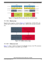
2.1.2.2 Power domains
While many systems have only one power supply voltage, they typically have “clean”
and “noisy” sections. The definitions of “clean” and “noisy” are not important – the
concept is that noise from one section should not interfere with another. In general, AC
power should be separated from DC power and digital should be separated from analog.
Power domain isolation is described in more detail in Freescale application note AN2764,
"Improving the Transient Immunity Performance of Microcontroller-Based
Applications." The basic concept is to isolate or place a low pass filter between power
domains. The AC power domain should be physically isolated from the DC domains.
Physical separation or decoupling filters (Figure 2-1) should be used to separate different
DC functional blocks (power domains) when necessary. Note that the Tower System
boards have multiple decoupling filters to separate digital and analog domains. Also note
that decoupling may not be needed in many applications – physical separation of domains
may be sufficient.
Kinetis Quick Reference User Guide, Rev. 2, 08/2012
22
Freescale Semiconductor, Inc.
Chapter 2 General System Setup (Hardware Considerations)
Figure 2-1. Generic decoupling filter
In general, the decoupling network series elements are small inductors or ferrite beads
that have a small impedance (about 100 Ω at 100 MHz). The capacitors are generally
10nF to 1uF and do not have to be the same value on both sides of the filter – select a
lower value for the side that has the higher frequency content.
2.1.3 PCB routing considerations
This section covers critical power and filtering aspects of PCB layout.
2.1.3.1 Power supply routing
Routing of power and ground to digital systems is a topic that is discussed and debated in
many textbooks and references. The basic concept is to ensure that the MCU and other
digital components have a low impedance path to the power supply. The typical guidance
that was given for one and two layer PCBs was to use wide traces and few layer
transitions. The recommendations for today’s high speed MCUs follow those given for
high speed microprocessor systems – specifically, use planes for power and ground. This
may raise the PCB cost, but the benefits of crosstalk reduction, reduction of RF
emissions, and improved transient immunity can be realized with lower overall
production and maintenance costs.
In general, the ground routing should take precedence over any other routing. Ground
planes or traces should never be broken by signals. For packages with leads, like the
LQFP, a ground plane directly below the MCU package is recommended to reduce RF
emissions and improve transient immunity. All of the VSS pins of the MCU should be
tied to a ground plane. Ground traces (from a plane) should be kept as short as possible as
they are routed to circuitry on signal layers (top and bottom). Power planes may be
broken to supply different voltages. All of the VDD pins of the MCU should be tied to
Kinetis Quick Reference User Guide, Rev. 2, 08/2012
Freescale Semiconductor, Inc.
23
Hardware considerations
the proper power plane. Power traces (from the planes) should be kept as short as
possible as they are routed to circuitry (pullups, filters, other logic & drivers) on the top
and bottom layers. More information is given in the PCB Layer Stack-up section below.
2.1.3.2 Power supply decoupling and filtering
As mentioned in the power domains section, decoupling networks are used to separate
domains. Bypass capacitors, while also called decoupling capacitors, are the storage
elements that provide the instantaneous energy demanded by the high speed digital
circuits.
Power supply bypass capacitors must be placed close to the MCU supply pins. The basic
concept is that the bypass capacitor provides the instantaneous current for every logic
transition within the MCU. Fortunately, each Kinetis MCU has a low voltage internal
regulator for the MCU core logic, so the abrupt current demands of the internal high
speed logic are not as critical. However, external signals demand energy from the power
rails when they transition from one logic level to the other. The bypass capacitors provide
the local filtering so that the effects of the external pin transitions are not reflected back
to the power supply, which causes RF emissions.
The basic rule of placing bypass capacitors as close as possible to the MCU is still
appropriate. The idea is to minimize the loop created by the capacitor between the VDD
and VSS pins. The implementation of this rule depends on the number of mounting
layers, how the supplies are routed, and the physical size of the capacitors:
• Number of mounting layers – PCBs with components mounted on the top side only
will have a significant limitation on how close the bypass caps can be located due to
the number of components that require space. PCBs that have components mounted
on both sides of the PCB allow closer placement of the bypass capacitors.
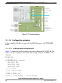
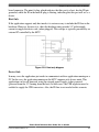
• Supply routing – With the Ball Grid Array (BGA) package, all of the VDD/VSS
pairs are routed to other layers under the package. This allows easier attachment of
the VDD and VSS pins to the power and ground planes within those layers. The
bypass capacitors can be placed in the area below the MCU, with connections very
close to the power pins. See Figure 2-2.
Kinetis Quick Reference User Guide, Rev. 2, 08/2012
24
Freescale Semiconductor, Inc.
Chapter 2 General System Setup (Hardware Considerations)
Figure 2-2. K60 TWR board top layer BGA pad arrangement
• Supply routing – For Quad Flat Pack (QFP) packages, the power supply pins may be
supplied radially to the MCU using traces rather than from planes. While it is
adequate to place the bypass capacitors close to the VDD and VSS pins on the traces
leading to the MCU, it is better to have the ground side of the bypass capacitor tied to
the ground plane (through a via and short trace) close to the VSS pin and the VDD
side tied to the power plane (through a via and short trace) close to the VDD pin.
2.1.3.3 Oscillators
The Kinetis MCU starts up with an internal digitally controlled oscillator (DCO) to
control the bus clocking, and then software is used to enable one or two external
oscillators if desired. The external oscillator for the Multipurpose Clock Generator
(MCG) module can range from a 32.768 kHz crystal up to a 32 MHz crystal or ceramic
resonator. The external oscillator for the Real Time Clock (RTC) module is a 32.768 kHz
crystal.
Kinetis Quick Reference User Guide, Rev. 2, 08/2012
Freescale Semiconductor, Inc.
25
Hardware considerations
2.1.3.3.1
RTC oscillator
The RTC oscillator connected to the EXTAL32 and XTAL32 pins is the simplest to
route. Both pins are located on outside ring pads on the BGA package, so the crystal can
be placed on the top layer of the PCB, close to the MCU. Since this oscillator does not
require any other external components the routing is straight from the crystal to the MCU
pins.
While the 32.768 kHz crystal is available in leaded cylindrical and surface mount
packaging, we recommend using the cylindrical package to simplify placement and
routing. The EXTAL32 and XTAL32 pins can be brought out directly from the MCU and
the crystal can be placed as close as possible to the MCU, which improves noise
immunity. Surface mount crystals may have pad spacing that is further apart than the
leaded crystals, making the routing and placement more complex.
2.1.3.3.2
MCG oscillator
While the RTC oscillator can also be used as a source for the MCG module, it is limited
to 32 kHz. The high speed oscillator that can be used to source the MCG module is very
versatile. The component choices for this oscillator are detailed in the device-specific
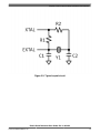
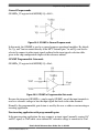
reference manual. The placement of this crystal or resonator is described here.
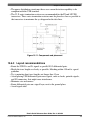
The EXTAL and XTAL pins are located on the outside pad ring of the BGA package and
on corner pins of the QFP package. This allows room for placement and routing of the
crystal or resonator on the top layer, close to the MCU. The feedback resistor and load
capacitors, if needed, can be placed on the top layer as well. See Figure 2-3, Figure 2-4,
and Figure 2-5.
Note that the low power modes of this oscillator do not require a feedback resistor, and
may not require external load capacitors. (Check the device-specific reference manual for
details.) This makes it as simple as possible since only one component has to be placed
and routed. Low power oscillators are more susceptible to interference by system
generated noise, so the guidelines for crystal routing are important.
The crystal or resonator should be located close to the MCU. No signals of any kind
should be routed on the layer directly below the crystal. A ground plane on the layer
directly below the crystal is recommended. A guard ring should be placed around the
crystal and its load components to protect it from crosstalk from adjacent signals on the
mounting layer. This guard ring can originate from the VSS pin adjacent to the crystal
pins. Note that the guard ring (and load capacitors) is connected to the ground plane in
Figure 2-4 and Figure 2-5.
Kinetis Quick Reference User Guide, Rev. 2, 08/2012
26
Freescale Semiconductor, Inc.
Chapter 2 General System Setup (Hardware Considerations)
Figure 2-3. Typical crystal circuit
Kinetis Quick Reference User Guide, Rev. 2, 08/2012
Freescale Semiconductor, Inc.
27
Hardware considerations
Figure 2-4. Potential crystal layout for BGA
Kinetis Quick Reference User Guide, Rev. 2, 08/2012
28
Freescale Semiconductor, Inc.
Chapter 2 General System Setup (Hardware Considerations)
Figure 2-5. Potential crystal layout for LQFP
2.1.3.4 General filtering
General purpose I/O pins should have adequate isolation and filtering from transients.
2.1.3.4.1
RESET_b and NMI_b
Critical input pins, like RESET_b and NMI_b should have 100 nF capacitors close to the
MCU for transient protection. Each pin has a weak internal pullup, but an external 4.7 kΩ
to 10 kΩ pullup is recommended. As with power pin filtering, it is recommended to
minimize the ground loop for the capacitor and the VDD loop for the pullup resistor for
these pins.
Kinetis Quick Reference User Guide, Rev. 2, 08/2012
Freescale Semiconductor, Inc.
29
Hardware considerations
The RESET_b pin also has a configurable digital filter to reject potential noise on this
input after power-up. The configuration bits are located in the SIM_SOPT6 register.
While use of this filter may negate the need for the pullup and capacitor mentioned
above, it is still recommended to use external filtering in electrically noisy environments.
2.1.3.4.2
General purpose I/O
General purpose inputs, such as low speed inputs, timer inputs, and signals from offboard should have low pass filters (series resistor and capacitor to ground) to prevent data
corruption due to crosstalk or transients. The filter capacitor should be placed close to the
MCU pin, while the resistor can be placed closer to the source.
Inputs that come from connectors should have low pass filtering at the connector to
prevent noise from propagating onto the PCB. This requires a robust ground structure
around the connector. Series resistors for signals that come from off-board should be
placed as close to the connector as possible. A filter cap closer to the MCU input pin may
be required if the signal trace length is very long and can pick up noise from other
circuits.
Output pins should not have any significant capacitance placed close to the MCU. These
signals can have capacitors at the load or connector to minimize radiated emissions if
necessary.
2.1.3.4.3
Analog inputs
Analog inputs should have low pass filters as well. The challenge with analog inputs,
especially for high resolution analog-to-digital conversions, is that the filter design needs
to consider the source impedance and sample time rather than a simple cutoff frequency.
This topic cannot be discussed in detail here, but the general concept is that fast sample
times will require smaller capacitor values and source impedances than slow sample
times. Higher resolution inputs may require smaller capacitor values and source
impedances than lower resolution inputs.
In general, capacitor values can range from 10 pF for high speed conversions to 1µF for
low speed conversions. Series resistors can range from a few hundred Ohms to 10 kΩ.
2.1.4 PCB layer stack-up
The Kinetis MCUs are high speed integrated circuits. Care must be taken in the PCB
design to ensure that fast signal transitions (rise/fall times and continuous frequencies) do
not cause RF emissions. Likewise, transient energy that enters the system needs to be
suppressed before it can affect the system operation (compatibility). The guidance from
Kinetis Quick Reference User Guide, Rev. 2, 08/2012
30
Freescale Semiconductor, Inc.
Chapter 2 General System Setup (Hardware Considerations)
high speed PCB designers is to have all signals routed within one dielectric (core or
prepreg) of a return path, which usually is a ground plane. This allows return currents to
predictably flow back to the source without affecting other circuits, which is the primary
cause of radiated emissions in electronic systems. This approach requires full planes
within the PCB layer stack and partial planes (copper pours) on signal layers where
possible. All ground planes and ground pours must be connected with plenty of vias.
Likewise, all “like” power planes and power pours must be connected with plenty of vias.
Recommended layer stackups:
4-Layer PCB A:
Layer 1 (top – MCU location)—Ground plane and pads for top mounted
components, no signals
Layer 2 (inner)—signals and power plane
Thick core
Layer 3 (inner)—signals and power plane
Layer 4 (bottom)—ground plane and pads for bottom mounted components, no
signals
4-Layer PCB B:
Layer 1 (top – MCU location)—signals and poured power
Layer 2 (inner)—ground plane
Thick core
Layer 3 (inner)—ground plane
Layer 4 (bottom)—signals and poured power
6-Layer PCB A:
Layer 1 (top – MCU)—power plane and pads for top mounted components, no
signals
Layer 2 (inner)—signals and ground plane
Layer 3 (inner)—power plane
Layer 4 (inner)—ground plane
Layer 5 (inner)—signals and power plane
Layer 6 (bottom)—ground plane and pads for bottom mounted components, no
signals
6-Layer PCB B:
Layer 1 (top – MCU)—signals and power plane
Layer 2 (inner)—ground plane
Layer 3 (inner)—signals and power plane
Layer 4 (inner)—ground plane
Layer 5 (inner)—power plane
Layer 6 (bottom)—signals and ground plane
Kinetis Quick Reference User Guide, Rev. 2, 08/2012
Freescale Semiconductor, Inc.
31
Hardware considerations
6-Layer PCB C:
Layer 1 (top – MCU)—signals and power plane
Layer 2 (inner)—ground plane
Layer 3 (inner)—signals and power plane
Layer 4 (inner)—signals and ground plane
Layer 5 (inner)—power plane
Layer 6 (bottom)—signals and ground plane
8-Layer PCB A:
Layer 1 (top – MCU)—signals
Layer 2 (inner)—ground plane
Layer 3 (inner)—signals
Layer 4 (inner)—power plane
Layer 5 (inner)—ground plane
Layer 6 (inner)—signals
Layer 7 (inner)—ground plane
Layer 8 (bottom)—signals
8-Layer PCB B:
Layer 1 (top – MCU)—signals and power plane
Layer 2 (inner)—ground plane
Layer 3 (inner)—signals and power plane
Layer 4 (inner)—ground plane
Layer 5 (inner)—power plane
Layer 6 (inner)—signals and ground plane
Layer 7 (inner)—power plane
Layer 8 (bottom)—signals and ground plane
8-Layer PCB C:
Layer 1 (top – MCU)—signals and ground plane
Layer 2 (inner)—power plane
Layer 3 (inner)—ground plane
Layer 4 (inner)—signals
Thick core
Layer 5 (inner)—signals
Layer 6 (inner)—ground plane
Layer 7 (inner)—power plane
Layer 8 (bottom)—signals and ground plane
8-Layer PCB D:
Layer 1 (top – MCU)—signals and ground plane
Layer 2 (inner)—power plane
Layer 3 (inner)—ground plane
Kinetis Quick Reference User Guide, Rev. 2, 08/2012
32
Freescale Semiconductor, Inc.
Chapter 2 General System Setup (Hardware Considerations)
Layer 4 (inner)—signals and power plane
Thick core
Layer 5 (inner)—signals and power plane
Layer 6 (inner)—ground plane
Layer 7 (inner)—power plane
Layer 8 (bottom)—signals and ground plane
In general, avoid placing one signal layer adjacent to another signal layer.
2.1.5 Other module hardware considerations
2.1.5.1 VBAT
The VBAT input supplies power to the RTC and a 32-byte register file during
powerdown and low power modes. This pin can be sourced from the VDD supply or
from a dedicated back-up battery cell. A simple battery isolator consists of a dual
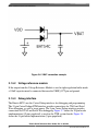
Schottky array with common cathodes. The TWR board example below (Figure 2-6) uses
the BAT54C device to provide battery back-up when the main system power is off. A
100 nF bypass capacitor, placed as near as possible to the MCU, is recommended to
minimize the effects of supply switching events.
Kinetis Quick Reference User Guide, Rev. 2, 08/2012
Freescale Semiconductor, Inc.
33
Other module hardware considerations
Figure 2-6. VBAT connection example
2.1.5.2 Voltage reference module
If the output from the Voltage Reference Module is used in tight-regulation buffer mode
a 100nF capacitor must be connected between the VREF_OUT pin and ground.
2.1.5.3 Debug interface
The Kinetis MCUs use the Cortex Debug interfaces for debugging and programming.
The 19-pin Cortex Debug+ETM interface provides connections for JTAG and Serial
Wire debugging, as well as target power. The 9-pin Cortex Debug interface provides
connections for JTAG and Serial Wire debugging. Figure 2-7 shows the 20-pin header
implementation (19 pins populated) as used on the TWR system boards. Figure 2-8
shows the 10-pin header implementation (9 pins populated).
Kinetis Quick Reference User Guide, Rev. 2, 08/2012
34
Freescale Semiconductor, Inc.
Chapter 2 General System Setup (Hardware Considerations)
Figure 2-7. 20-pin debug interface
Figure 2-8. 10-pin debug interface
The debug signals are multiplexed with general purpose I/O pins, so some signals will
require proper biasing to select the operating mode. The JTAG_TMS signal on PTA3
requires a strong pullup resistor for mode selection. The Cortex Debug specification
recommends that the JTAG_TCLK and JTAG_TDI pins (on PTA0 and PTA1) have pull
resistors (high or low) to force a known state on these debug input pins. Note that the
RESET_b signal in the debug interface is the MCU’s reset pin and not the JTAG_TRST
signal. The connectors for this interface are keyed dual row 0.050” centered headers.
When implementing either of these headers on a target system, pin 7 must be depopulated
to use the 19-pin or 9-pin adapters from the debug tool. The Samtec part numbers for
these connectors are:
• FTSH-110-01-L-DV-K – 20-pin keyed connector
• FTSH-105-01-L-DV-K – 10-pin keyed connector
Kinetis Quick Reference User Guide, Rev. 2, 08/2012
Freescale Semiconductor, Inc.
35
Other module hardware considerations
• FTSH-110-01-L-DV – 20-pin connector, no key
• FTSH-105-01-L-DV – 10-pin connector, no key
This interface is useful during the development phase of a project. The header may not
need to be populated in the production phase of the project, but the PCB pads should be
kept available for future debugging purposes.
Kinetis Quick Reference User Guide, Rev. 2, 08/2012
36
Freescale Semiconductor, Inc.
Chapter 3
Nested Vector Interrupt Controller (NVIC)
3.1 NVIC
3.1.1 Overview
This chapter shows how the NVIC is integrated into the Kinetis MCUs and how to
configure it and set-up module interrupts. It also demonstrates the steps to set the
interrupts for the desired peripheral and how to locate the vector table from flash to
RAM.
3.1.1.1 Introduction
The NVIC is a standard module on the ARM Cortex M series. This module is closely
integrated with the core and provides a very low latency for entering an interrupt service
routine ISR (12 cycles) and exiting an ISR (12 cycles).
The NVIC provides 16 different interrupt priorities. Priority 0 is the highest and the
lowest is15. This can be used to control which interrupt must be serviced. For example,
on a motor-control application if a UART and a timer interrupt occur at the same time,
serving the timer interrupt that moves the motor is more critical than the UART interrupt
that just received a character. In this case, the timer priority must be set higher than the
UART.
3.1.1.2 Features
On Kinetis MCUs the NVIC provides up to 120 interrupt sources including 16 that are
core specific. It also implements up to 16 priority levels that are fully programmable. The
NVIC uses a vector table to manage the interrupts. This vector table can be stored in
either flash or RAM, depending on the application.
Kinetis Quick Reference User Guide, Rev. 2, 08/2012
Freescale Semiconductor, Inc.
37
NVIC
Table 3-1. Core exceptions
Address
Vector
IRQ
Source module
Source description
0
—
ARM core
Initial stack pointer
1
—
ARM core
Initial program Counter
2
—
ARM core
NMI
3
—
ARM core
Hard fault
4
—
ARM core
Memory manage fault
5
—
ARM core
Bus fault
6
—
ARM core
Usage fault
11
—
ARM core
SVCall
12
—
ARM core
Debug monitor
14
—
ARM core
Pendable request for system service
15
—
ARM core
System tick timer
ARM Core System Handler Vectors
0x0000_0000
3.1.2 Configuration examples
The NVIC is easy to configure. Two examples are shown in this section. The first
example shows how to configure the NVIC for a module. The low power timer (LPTMR)
is used as the base for this example. The second example shows how to locate the vector
table from the flash to RAM.
3.1.2.1 Configuring the NVIC
Configuring the NVIC for the specific module involves writing three registers:
NVICSERx (NVIC Set Enable Register), NVICCPRx (NVIC Clear Pending Register),
and NVICIPxx (NVIC Interrupt Priority). After the NVIC is configured and the desired
peripheral has its interrupts enabled, the NVIC serves any pending request from that
module by going to the module's ISR.
3.1.2.1.1
Code example and explanation
This example shows how to set up the NVIC for a specific module. In this case the
LPTMR is used.
The steps to configure the NVIC for this module are:
1. Identify the vector number and the IRQ number of the module from the vector table
in the device-specific reference manual in the section Interrupt Channel
Assignments. For the LPTMR the vector is 101.
Kinetis Quick Reference User Guide, Rev. 2, 08/2012
38
Freescale Semiconductor, Inc.
Chapter 3 Nested Vector Interrupt Controller (NVIC)
Table 3-2. LPTMR
vector
Address
Vector
IRQ
Source Module
Source
Description
0x0000_018C
99
83
TSI
Single interrupt
Source
0x0000_0190
100
84
MCG
0x0000_0194
101
85
LPTMR
2. Determine which NVICSERx register contains the IRQ. Each NVICSERx register
contains 32 IRQs. Therefore, the NVICSER0 can enable from IRQ 0 to IRQ 31, the
NVICSER1 from IRQ 32 to IRQ 63, and NVICSER2 from IRQ 64 to IRQ 95. For
this example, the NVICSER2 is used because the LPTMR IRQ is 85. The
NVICCPRx takes on the same number, in this case NVICCPR2.
3. To know which bit to set perform a modulo operation to obtain the remainder by 32
of the IRQ number. This number is used to enable the interrupt on NVICSER2 and to
clear the pending interrupts from NVICCPR2.
Example:
LPTMR BIT = 85 mod 32
LPTMR BIT = 21
4. At this point, the interrupt for the LPTMR can be configured:
NVICICPR2|=(1<<21);
NVICISER2|=(1<<21);
//Clear any pending interrupts on LPTMR
//Enable interrupts from LPTMR module
5. Next, set the interrupt priority level. This is application dependent. On Kinetis MCUs
there are 16 different priority levels. To set the priority, write to the NVICIPxx
register, the “xx” represents the IRQ number, in this example, NVICIP85. Note the
most significant nibble is used to set-up the priority, the lower nibble is reserved and
reads as zero. The LPTMR example sets the priority to 3:
NVICIP85 = 0x30;
//Set Priority 3 to the LPTMR module
6. After the NVIC registers are set-up, finish the peripheral configuration that must
enable the interrupt.
7. In the ISR, clear the peripheral interrupt flag to avoid re-entrance. For this example:
void vfnLPTMR_ISR (void)
{
LPTMR0_CSR|=LPTMR_CSR_TCF_MASK;
/*ISR code goes here*/
}
//Clear LPTMR Compare flag
Kinetis Quick Reference User Guide, Rev. 2, 08/2012
Freescale Semiconductor, Inc.
39
NVIC
3.1.2.2 Relocating the vector table
Some applications need the vector table to be located in RAM. For example in an RTOS
implementation, the vector table needs to be in RAM, this allows the Kernel to install
ISRs by modifying the vector table during runtime.
The NVIC provides a simple way to reallocate the vector table, for this purpose the user
needs to set up the Vector Table Offset Register (VTOR) with the address offset for the
new position. Use the bit TBLBASE[29] to indicate the table is either on RAM with 1 or
flash with 0 and the TBLOFF[28:7] to indicate the address offset for the table.
The Cortex-M4 assumes the RAM starts at 0x20000000 and expects the vector table to be
stored in that address if the VTOR TBLBASE[29] bit is set. Because the Kinetis MCU
family RAM starts at 0x1fff0000, this bit must be cleared.
If the vector table is planned to be stored in RAM, you must the table copy from the flash
to RAM. Also note that in some low power modes, a portion of the RAM will not be
powered, which can lead to a vector table corruption. In this case, locate the vector table
in the flash prior to entering a low power mode.
3.1.2.2.1 Code example and explanation
The vector table is usually in flash after reset, This indicates that moving the table from
flash to RAM is the most common action. To achieve this, two steps must be performed:
1. Copy from flash to RAM the entire vector table. The linker command file labels are
useful in this step. This is what the code looks like:
/*Address for VECTOR_TABLE and VECTOR_RAM come from the linker file*/
extern uint32 __VECTOR_TABLE[];
extern uint32 __VECTOR_RAM[];
/* Copy the vector table to RAM */
if (__VECTOR_RAM != __VECTOR_TABLE)
{
for (n = 0; n < 0x410; n++)
__VECTOR_RAM[n] = __VECTOR_TABLE[n];
}
2. After the table has been copied, set the proper offset for the VTOR register:
/* Set the VTOR to be on RAM */
SCB_VTOR = __VECTOR_RAM;
It is important to follow the above mentioned steps in the order indicated. This ensures
there is always a valid vector table.
Kinetis Quick Reference User Guide, Rev. 2, 08/2012
40
Freescale Semiconductor, Inc.
Chapter 3 Nested Vector Interrupt Controller (NVIC)
3.1.2.3 Disabling priorities
There are applications with important code where just certain interrupt priorities are
allowed to interrupt, this is because these interrupts are more critical to the application. In
other cases, all the interrupts need to be disabled to ensure the code is atomic, for
example, a context switch on Operating Systems. The Cortex M4 provides the BASEPRI
register that allows disabling lower interrupt priorities from any priority you choose or
the option of disabling them all.
The BASEPRI is used as the NVICIPxx register. Therefore, 16 interrupt priorities can be
masked and only the most significant nibble is used.
Please note that BASEPRI does not disable any of the fixed priority exceptions as Reset
(priority -3), a non-maskable interrupt (NMI) (priority -2), and Hard Fault (priority -1).
BASEPRI can be set only in privilege mode. The reset value is 0x00, therefore all
interrupts are enabled.
3.1.2.3.1 Code example and explanation
To set up BASEPRI a function from your development tools can be used. For example in
IAR tools, the function is called __set_BASEPRI.
1. For disabling lower interrupt priorities set the lowest priority level that the
application allows. For example, priority 5 – 0 are allowed. BASEPRI must take the
priority 5.
/* Disable interrupts priorities from 0x06 – 0x0F */
__set_BASEPRI(0x50);
2. For disabling all priorities to ensure atomic code, the BASEPRI must take the
maximum priority value available, for Kinetis MCUs which is priority 15
/* Disable all interrupt priorities */
__set_BASEPRI(0xF0);
Kinetis Quick Reference User Guide, Rev. 2, 08/2012
Freescale Semiconductor, Inc.
41
NVIC
Kinetis Quick Reference User Guide, Rev. 2, 08/2012
42
Freescale Semiconductor, Inc.
Chapter 4
Clocking System
4.1 Clocking
4.1.1 Overview
This chapter will demonstrate how to configure the Clocking System and the
Multipurpose Clock Generator (MCG) module in various modes that a typical application
may require. The examples will show how to enable the on-chip PLL for high-speed
operation and how to move backwards and forwards between using the PLL and a low
power/low speed mode for entering very low power run mode (VLPR). Also, an example
is provided of how to configure the frequency-locked loop (FLL) as the main system
clock source, using the RTC oscillator as the reference clock.
4.1.2 Features
The clocking system is summarized in Figure 4-1.
Kinetis Quick Reference User Guide, Rev. 2, 08/2012
Freescale Semiconductor, Inc.
43
Clocking
SIM
Fast IRC
MCGIRCLK
CG
Slow IRC
MCGFFCLK
÷2
FLL
OUTDIV1
CG
Core / system clocks
OUTDIV2
CG
Bus clock
OUTDIV3
CG
FlexBus clock
OUTDIV4
CG
Flash clock
MCGOUTCLK
PLL
MCGFLLCLK
FRDIV
MCGPLLCLK
MCGPLLCLK/
MCGFLLCLK
System oscillator
EXTAL
OSCCLK
XTAL_CLK
XTAL
EXTAL32
XTAL32
OSC
logic
CG
Clock options for
some peripherals
OSCERCLK
OSC32KCLK
ERCLK32K
RTC oscillator
PMC
OSC logic
PMC logic
Clock options for some
peripherals
MCG
LPO
Real-time clock
CG — Clock gate
Figure 4-1. Clock distribution diagram
The system level clocks are provided by the MCG. The MCG consists of:
• Two individually trimable internal reference clocks (IRC), a slow IRC with a
frequency of ~32 kHz and a fast IRC with a frequency of ~4 MHz (with a fixed
divide by 2).
• Frequency locked loop (FLL) using the slow IRC or an external source as the
reference clock.
• Phase locked loop (PLL) using an external source as the reference clock.
• Auto trim machine (ATM) to allow both of the IRCs to be trimmed to a custom
frequency using an externally-generated reference clock.
The clocks provided by the MCG are summarized as follows:
• MCGOUTCLK – this is the main system clock used to generate the core, bus, and
memory clocks. It can be generated from one of the on-chip reference oscillators, the
on-chip crystal/resonator oscillator, an externally generated square wave clock, the
FLL, or the PLL.
• MCGFLLCLK – this is the output of the FLL and is available any time the FLL is
enabled.
Kinetis Quick Reference User Guide, Rev. 2, 08/2012
44
Freescale Semiconductor, Inc.
Chapter 4 Clocking System
• MCGPLLCLK – this is the output of the PLL and is available any time the PLL is
enabled.
• MCGIRCLK – this is the output of the selected IRC. The selected IRC will be
enabled whenever this clock is selected.
• MCGFFCLK – this is either the slow IRC or the external clock source divided by the
FLL external reference divider (FRDIV). This clock is available in all modes except
FLL bypassed internal (FBI) and bypassed low power internal (BLPI) when the slow
IRC is selected. The source of this clock is selected by the value of the internal
reference select bit (IREFS).
In addition to the clocks provided by the MCG, there are three other system level clock
sources available for use by various peripheral modules:
• OSCERCLK – this is the clock provided by the system oscillator and is the output of
the oscillator or the external square wave clock source.
• ERCLK32K – this is the output of the RTC oscillator or the system oscillator if it is
set to provide a 32 kHz clock in low power mode.
• LPO – this is the output of the low power oscillator. It is an on-chip, very low power
oscillator with an output of approximately 1 kHz that is available in all run and low
power modes.
4.1.3 Configuration examples
The MCG can be configured in one of several modes to provide a flexible means of
providing clocks to the system for a wide range of applications. Some of the more
commonly used modes are described in the following configuration examples.
After exiting reset, or recovering from a very low leakage state, the MCG will be in FLL
engaged internal (FEI) mode with MCGCLKOUT at 20.97 MHz, assuming a factory
trimmed slow IRC frequency of 32.768 kHz. If a different MCG mode is required, the
MCG can be transitioned to that mode under software control.
Although not included in the sample code, you should include a “timeout” mechanism
when checking the status bits within the MCG. After making changes to clock selection
bits, enabling the oscillator or the PLL, the appropriate status bits should be verified
before continuing. If for some reason the bit being checked does not update, the “while
loop” will never exit unless a timeout mechanism is used. A timeout counter should be
started before checking the status bits. This counter must then be stopped and reset after
the loop exits. If a timeout is generated, a decision can be made about what to do
depending on the status bits that failed to update. For example, if the oscillator does not
start due to a damaged PCB trace, the decision to continue with an internal-only clocking
mode can be made with an appropriate indication to the user or a central monitoring
station.
Kinetis Quick Reference User Guide, Rev. 2, 08/2012
Freescale Semiconductor, Inc.
45
Clocking
4.1.3.1 Transitioning to PLL engaged external mode
PLL engaged external mode uses an external clock, from either the crystal oscillator or an
externally generated square wave, as the reference for the on-chip PLL. An on-chip
divider allows an external clock to provide the reference clock to the PLL within the
required range of 2–4 MHz. The PLL provides the most accurate clock source for
frequencies greater than can be generated by an external source. In this example, an 8
MHz crystal is used to generate a 96 MHz system clock. The system clock dividers are
set to allow the maximum system performance with this clock source. The PLL
frequency can be divided down to provide the USB clock of 48 MHz. The MCG is
configured to minimize PLL jitter (maximum PLL frequency with the minimum
multiplication factor).
4.1.3.1.1
Code example and explanation
// If the internal load capacitors are being used, they should be selected
// before enabling the oscillator. Application specific. 16 pF and 8 pF selected
// in this example
OSC_CR = OSC_CR_SC16P_MASK | OSC_CR_SC8P_MASK;
// Enabling the oscillator for 8 MHz crystal
// RANGE=1, should be set to match the frequency of the crystal being used
// HGO=1, high gain is selected, provides better noise immunity but does draw
// higher current
// EREFS=1, enable the external oscillator
// LP=0, low power mode not selected (not actually part of osc setup)
// IRCS=0, slow internal ref clock selected (not actually part of osc setup)
MCG_C2 = MCG_C2_RANGE(1) | MCG_C2_HGO_MASK | MCG_C2_EREFS_MASK;
//
//
//
//
//
//
//
Select ext oscillator, reference divider and clear IREFS to start ext osc
CLKS=2, select the external clock source
FRDIV=3, set the FLL ref divider to keep the ref clock in range
(even if FLL is not being used) 8 MHz / 256 = 31.25 kHz
IREFS=0, select the external clock
IRCLKEN=0, disable IRCLK (can enable it if desired)
IREFSTEN=0, disable IRC in stop mode (can keep it enabled in stop if desired)
MCG_C1 = MCG_C1_CLKS(2) | MCG_C1_FRDIV(3);
// wait for oscillator to initialize
while (!(MCG_S & MCG_S_OSCINIT_MASK)){}
// wait for Reference clock to switch to external reference
while (MCG_S & MCG_S_IREFST_MASK){}
// Wait for MCGOUT to switch over to the external reference clock
while (((MCG_S & MCG_S_CLKST_MASK) >> MCG_S_CLKST_SHIFT) != 0x2){}
// Now configure the PLL and move to PBE mode
// set the PRDIV field to generate a 4 MHz reference clock (8 MHz /2)
MCG_C5 = MCG_C5_PRDIV(1); // PRDIV=1 selects a divide by 2
//
//
//
//
set the VDIV field to 0, which is x24, giving 4 x 24 = 96 MHz
the PLLS bit is set to enable the PLL
the clock monitor is enabled, CME=1 to cause a reset if crystal fails
LOLIE can be optionally set to enable the loss of lock interrupt
MCG_C6 = MCG_C6_CME_MASK | MCG_C6_PLLS_MASK;
Kinetis Quick Reference User Guide, Rev. 2, 08/2012
46
Freescale Semiconductor, Inc.
Chapter 4 Clocking System
// wait until the source of the PLLS clock has switched to the PLL
while (!(MCG_S & MCG_S_PLLST_MASK)){}
// wait until the PLL has achieved lock
while (!(MCG_S & MCG_S_LOCK_MASK)){}
// set up the SIM clock dividers BEFORE switching to the PLL to ensure the
// system clock speeds are in spec.
// core = PLL (96 MHz), bus = PLL/2 (48 MHz), flexbus = PLL/2 (48 MHz), flash = PLL/4 (24
MHz)
SIM_CLKDIV1 = SIM_CLKDIV1_OUTDIV1(0) | SIM_CLKDIV1_OUTDIV2(1)
| SIM_CLKDIV1_OUTDIV3(1) | SIM_CLKDIV1_OUTDIV4(3);
// Transition into PEE by setting CLKS to 0
// previous MCG_C1 settings remain the same, just need to set CLKS to 0
MCG_C1 &= ~MCG_C1_CLKS_MASK;
// Wait for MCGOUT to switch over to the PLL
while (((MCG_S & MCG_S_CLKST_MASK) >> MCG_S_CLKST_SHIFT) != 0x3){}
// The USB clock divider in the System Clock Divider Register 2 (SIM_CLKDIV2)
// should be configured to generate the 48 MHz USB clock before configuring
// the USB module.
SIM_CLKDIV2 |= SIM_CLKDIV2_USBDIV(1); // sets USB divider to /2 assuming reset
// state of the SIM_CLKDIV2 register
4.1.3.2 Transitioning between PLL engaged external mode and
bypassed low power internal mode
To be able to move the MCU into the VLPR (or wait) mode, the MCG must be set in a
low-power, low-frequency mode with MCGCLKOUT <= 2 MHz. This mode is provided
by means of selecting the fast IRC when the MCG is set in BLPI mode. This example
shows how to move to this clock mode from PLL engaged external mode before entering
VLPR and then returns to that mode after VLPR is exited. In VLPR mode, the system
clock dividers cannot be changed. These dividers should be configured when the MCG is
in BLPI mode before the MCU power mode is changed to VLPR.
4.1.3.2.1
Code example and explanation
// Moving from PEE to BLPI
// first move from PEE to PBE
MCG_C1 |= MCG_C1_CLKS(2); // select external reference clock as MCG_OUT
// Wait for clock status bits to update indicating clock has switched
while (((MCG_S & MCG_S_CLKST_MASK) >> MCG_S_CLKST_SHIFT) != 0x2){}
// now move to FBE mode
// make sure the FRDIV is configured to keep the FLL reference within spec.
MCG_C1 &= ~MCG_C1_FRDIV_MASK; // clear FRDIV field
MCG_C1 |= MCG_C1_FRDIV(3); // set FLL ref divider to 256
MCG_C6 &= ~MCG_C6_PLLS_MASK; // clear PLLS to select the FLL
while (MCG_S & MCG_S_PLLST_MASK){} // Wait for PLLST status bit to clear to
// indicate switch to FLL output
// now move to FBI mode
MCG_C2 |= MCG_C2_IRCS_MASK; // set the IRCS bit to select the fast IRC
// set CLKS to 1 to select the internal reference clock
// keep FRDIV at existing value to keep FLL ref clock in spec.
// set IREFS to 1 to select internal reference clock
MCG_C1 = MCG_C1_CLKS(1) | MCG_C1_FRDIV(3) | MCG_C1_IREFS_MASK;
// wait for internal reference to be selected
Kinetis Quick Reference User Guide, Rev. 2, 08/2012
Freescale Semiconductor, Inc.
47
Clocking
while (!(MCG_S & MCG_S_IREFST_MASK)){}
// wait for fast internal reference to be selected
while (!(MCG_S & MCG_S_IRCST_MASK)){}
// wait for clock to switch to IRC
while (((MCG_S & MCG_S_CLKST_MASK) >> MCG_S_CLKST_SHIFT) != 0x1){}
// now move to BLPI
MCG_C2 |= MCG_C2_LP_MASK; // set the LP bit to enter BLPI
// set up the SIM clock dividers BEFORE switching to VLPR to ensure the
// system clock speeds are in spec. MCGCLKOUT = 2 MHz in BLPI mode
// core = 2 MHz, bus = 2 MHz, flexbus = 2 MHz, flash = 1 MHz
SIM_CLKDIV1 = SIM_CLKDIV1_OUTDIV1(0) | SIM_CLKDIV1_OUTDIV2(0)
| SIM_CLKDIV1_OUTDIV3(0) | SIM_CLKDIV1_OUTDIV4(1);
Now that MCGCLKOUT is at 2 MHz, the MCU VLPR power mode may be selected.
Refer to the power management controller for details on this. When the MCU transitions
back to normal run mode, the MCG will still be configured in BLPI mode. The MCG is
then configured in PLL engaged external mode by means of software as follows:
// Moving from BLPI to PEE
// first move to FBI
MCG_C2 &= ~MCG_C2_LP_MASK; // clear the LP bit to exit BLPI
// move to FBE
// clear IREFS to select the external ref clock
// set CLKS = 2 to select the ext ref clock as clk source
// it is assumed the oscillator parameters in MCG_C2 have not been changed
MCG_C1 = MCG_C1_CLKS(2) | MCG_C1_FRDIV(3);
// wait for the oscillator to initialize again
while (!(MCG_S & MCG_S_OSCINIT_MASK)){}
// wait for Reference clock to switch to external reference
while (MCG_S & MCG_S_IREFST_MASK){}
// wait for MCGOUT to switch over to the external reference clock
while (((MCG_S & MCG_S_CLKST_MASK) >> MCG_S_CLKST_SHIFT) != 0x2){}
//configure PLL and system clock dividers as FEI to PEE example
MCG_C5 = MCG_C5_PRDIV(1);
MCG_C6 = MCG_C6_PLLS_MASK;
while (!(MCG_S & MCG_S_PLLST_MASK)){}
while (!(MCG_S & MCG_S_LOCK_MASK)){}
// configure the clock dividers back again before switching to the PLL to ensure the system
// clock speeds are in spec.
// core = PLL (96 MHz), bus = PLL/2 (48 MHz), flexbus = PLL/2 (48 MHz), flash = PLL/4 (24
MHz)
SIM_CLKDIV1 = SIM_CLKDIV1_OUTDIV1(0) | SIM_CLKDIV1_OUTDIV2(1)
| SIM_CLKDIV1_OUTDIV3(1) | SIM_CLKDIV1_OUTDIV4(3);
MCG_C1 &= ~MCG_C1_CLKS_MASK;
while (((MCG_S & MCG_S_CLKST_MASK) >> MCG_S_CLKST_SHIFT) != 0x3){}
4.1.3.3 Configuring the FLL with the RTC oscillator as a reference
The MCG can generate all the system clocks using the FLL with the RTC oscillator being
used as the reference for it. This has the benefit that an accurate reference clock can be
used without the cost of additional external components in an application where the RTC
is already being used.
4.1.3.3.1
Code example and explanation
// Using the RTC OSC as Ref Clk
// Configure and enable the RTC OSC
// select the load caps (application dependent) and the oscillator enable bit
Kinetis Quick Reference User Guide, Rev. 2, 08/2012
48
Freescale Semiconductor, Inc.
Chapter 4 Clocking System
// note that other bits in this register may need to be set depending on the intended use of
the RTC
RTC_CR |= RTC_CR_SC16P_MASK | RTC_CR_SC8P_MASK | RTC_CR_OSCE_MASK;
time_delay_ms(1000); // wait for the RTC oscillator to initialize
// select the RTC oscillator as the MCG reference clock
SIM_SOPT2 |= SIM_SOPT2_MCGCLKSEL_MASK;
// ensure MCG_C2 is in the reset state, key item is RANGE = 0 to select the correct FRDIV
factor
MCG_C2 = 0x0;
//
//
//
//
//
//
Select the Reference Divider and clear IREFS to select the osc
CLKS=0, select the FLL as the clock source for MCGOUTCLK
FRDIV=0, set the FLL ref divider to divide by 1
IREFS=0, select the external clock
IRCLKEN=0, disable IRCLK (can enable if desired)
IREFSTEN=0, disable IRC in stop mode (can keep it enabled in stop if desired)
MCG_C1 = 0x0;
// wait for Reference clock to switch to external reference
while (MCG_S & MCG_S_IREFST_MASK){}
// Wait for clock status bits to update
while (((MCG_S & MCG_S_CLKST_MASK) >> MCG_S_CLKST_SHIFT) != 0x0){}
//
//
//
//
Can select
Must first
bus clocks
core = FLL
the FLL operating range/freq by means of the DRS and DMX32 bits
ensure the system clock dividers are set to keep the core and
within spec.
(48 MHz), bus = FLL (48 MHz), flexbus = PLL (48 MHz), flash = PLL/2 (24 MHz)
SIM_CLKDIV1 = SIM_CLKDIV1_OUTDIV1(0) | SIM_CLKDIV1_OUTDIV2(0)
| SIM_CLKDIV1_OUTDIV3(0) | SIM_CLKDIV1_OUTDIV4(1);
// In this example DMX32 is set and DRS is set to 1 = 48 MHz from a 32.768 kHz
// crystal
MCG_C4 |= MCG_C4_DMX32_MASK | MCG_C4_DRST_DRS(1);
4.1.4 Clocking system device hardware implementation
It is possible to provide all the system level clocks from internal sources. However, if the
PLL is to be used or an accurate reference clock is required, an external clock must be
provided. This can be from an externally generated clock source that provides a square
wave clock or it can be from an internal oscillator using an external crystal or resonator.
There are two independent on-chip crystal oscillators, one for the RTC and one to
provide a reference for the main system clocks.
The RTC clock source comes only from the dedicated RTC oscillator. In many cases, the
RTC oscillator will require only an external 32 kHz crystal. The oscillator feedback
resistor is integrated within the device along with selectable internal load capacitors.
The main system oscillator can be configured in various ways depending on the crystal
frequency and mode being used. Refer to the device-specific reference manual for details.
The main oscillator also has programmable internal load capacitors. When the main
oscillator is configured for low power an integrated oscillator feedback resistor is
provided.
Kinetis Quick Reference User Guide, Rev. 2, 08/2012
Freescale Semiconductor, Inc.
49
Clocking
The internal crystal load capacitors in both oscillators are selectable in software to
provide up to 30 pF, in 2 pF increments, for each of the EXTAL and XTAL pins. This
provides an effective series capacitive load of up to 15 pF. The parasitic capacitance of
the PCB should also be included in the calculation of the total crystal load. The
combination of these two values will often mean that no external load capacitors are
required.
If either of the main oscillator pins are not being used, they may be left unconnected in
their default reset configuration or may be used as general-purpose outputs (not inputs).
4.1.5 Layout guidelines for general routing and placement
Use the following general routing and placement guidelines when laying out a new
design. These guidelines will help to minimize electromagnetic compatibility (EMC)
problems.
• To minimize parasitic elements, surface mount components should be used where
possible
• All components should be placed as close to the MCU as possible.
• If external load capacitors are required, they should use a common ground
connection shared in the center
• If the crystal, or resonator, has a ground connection, it should be connected to the
common ground of the load capacitors
• Where possible:
• keep high-speed IO signals as far from the EXTAL and XTAL signals as
possible
• do not route signals under oscillator components - on same layer or layer below
• select the functions of pins close to EXTAL and XTAL to have minimal
switching to reduce injected noise
4.1.6 References
The following list of application notes associated with crystal oscillators are available on
the Freescale website at www.freescale.com. They discuss common oscillator
characteristics, potential problems and troubleshooting guidelines.
•
•
•
•
AN1706: Microcontroller Oscillator Circuit Design Considerations
AN1783: Determining MCU Oscillator Start-Up Parameters
AN2606: Practical Considerations for Working With Low-Frequency Oscillators
AN3208: Crystal Oscillator Troubleshooting Guide
Kinetis Quick Reference User Guide, Rev. 2, 08/2012
50
Freescale Semiconductor, Inc.
Chapter 5
Power Management Controller (PMC/MODECTL)
5.1 Using the power management controller
5.1.1 Overview
This section will demonstrate how to use the Power Management Controller (PMC)
module to protect the MCU from unexpected low VDD events. References to other
protection options will also be made.
5.1.1.1 Introduction
This chapter is a brief description of the power management features of the Kinetis 32-bit
MCU.
There are three modules covered in this chapter:
• Power Management Controller (PMC)
• Mode Controller (MC)
• Low Leakage Wakeup Unit (LLWU)
5.1.2 Using the low voltage detection system
5.1.2.1 Features
The LVD features includes the protection of memory contents from brown out conditions
and the operation of the MCU below the specified VDD levels. The user has full control
over the trip voltages of two detection circuits. The first is a warning detect circuit and
the second is reset detect circuit.
Kinetis Quick Reference User Guide, Rev. 2, 08/2012
Freescale Semiconductor, Inc.
51
Using the low voltage detection system
As voltage falls below the warning level the LVW circuit flags the warning event and can
cause an interrupt. If the voltage continues to fall, the LVD circuit flags the detect event
and can either cause a reset or an interrupt. The user can choose what action to take in the
interrupt service routine. If a detect is selected to drive reset, the LVD circuit holds the
MCU in reset until the supply voltage rises above the detect threshold.
There are two independent POR circuits for the MCU, one for VDD and another for
VBAT. The POR circuit for the MCU will hold the MCU in reset based upon the VDD
voltage. The POR circuit for VBAT will reset both the RTC and OSC2 modules, but will
not reset the MCU. If VBAT supply is not present, then accesses to the RTC registers
may not occur and could result in a core-lockup type reset in the MCU.
5.1.2.2 Configuration examples
LVD and LVW initialization code is given below: Notice the comments describing the
chosen settings. You should select the statement options for your application. The NVIC
vector flag may be set and should be cleared. The Interrupt is enabled in the NVIC in this
initialization.
void LVD_Init(void)
{ /* setup LVD
Low-Voltage Detect Voltage Select
Selects the LVD trip point voltage (VLVD).
00 Low trip point selected (VLVD = VLVDL)
01 High trip point selected (VLVD = VLVDH)
10 Reserved
11 Reserved
*/
/* Choose one of the following statements */
PMC_LVDSC1 |= PMC_LVDSC1_LVDRE_MASK ;
//Enable LVD Reset
// PMC_LVDSC1 &= ~PMC_LVDSC1_LVDRE_MASK ;
//Disable LVD Reset
/* Choose one of the following statements */
//PMC_LVDSC1 |= PMC_LVDSC1_LVDV_MASK & 0x01; //High Trip point 2.48V
PMC_LVDSC1 &= PMC_LVDSC1_LVDV_MASK & 0x00; //Low Trip point 1.54 V
/* Choose one of the following statements */
PMC_LVDSC2 = PMC_LVDSC2_LVWACK_MASK | PMC_LVDSC2_LVWV(0);
//0b00 low trip point LVWV
//PMC_LVDSC2 = PMC_LVDSC2_LVWACK_MASK | PMC_LVDSC2_LVWV(1);
//0b01 mid1 trip point LVWV
//PMC_LVDSC2 = PMC_LVDSC2_LVWACK_MASK | PMC_LVDSC2_LVWV(2);
//0b01000010 mid2 trip point LVWV
//PMC_LVDSC2 = PMC_LVDSC2_LVWACK_MASK | PMC_LVDSC2_LVWV(3);
//0b01000011 high trip point LVWV
// ack to clear initial flags
PMC_LVDSC1 |= PMC_LVDSC1_LVDACK_MASK; // clear detect flag if present
PMC_LVDSC2 |= PMC_LVDSC2_LVWACK_MASK; // clear warning flag if present
/*
LVWV if LVDV high range selected
Low trip point selected (VLVW = VLVW1)
Mid 1 trip point selected (VLVW = VLVW2)
Mid 2 trip point selected (VLVW = VLVW3)
High trip point selected (VLVW = VLV4)
LVWV if LVDV low range selected
Low trip point selected (VLVW = VLVW1)
-
2.62
2.72
2.82
2.92
- 1.74
Kinetis Quick Reference User Guide, Rev. 2, 08/2012
52
Freescale Semiconductor, Inc.
Chapter 5 Power Management Controller (PMC/MODECTL)
Mid 1 trip point selected (VLVW = VLVW2) - 1.84
Mid 2 trip point selected (VLVW = VLVW3) - 1.94
High trip point selected (VLVW = VLV4)
- 2.04
*/
NVICICPR0|=(1<<20);
NVICISER0|=(1<<20);
}
//Clear any pending interrupts on LVD
//Enable interrupts from LVD module
5.1.2.3 Interrupt code example and explanation
The LVD circuitry can be programmed to cause an interrupt. You should create a service
routine to clear the flags and react appropriately. An example of such an interrupt service
routine is given. Notice the NVIC module references. This clearing is redundant if the
module clearing is done correctly.
void pmc_lvd_isr(void){
printf("\rPMC_LVD ISR entered** ");
if ( PMC_LVDSC2 & PMC_LVDSC2_LVWF_MASK)
PMC_LVDSC2 |= PMC_LVDSC2_LVWACK_MASK;
if ( PMC_LVDSC1 & PMC_LVDSC1_LVDF_MASK)
PMC_LVDSC1 |= PMC_LVDSC1_LVDACK_MASK;
NVICICPR0|=(1<<20);
//Clear any pending interrupts on LVD
}
5.1.2.4 Hardware implementation
RESET PIN: The reset pin is driven out if the internal circuitry detects a reset. This is
true for all resets, including a reset that causes a recovery from the VLLSx modes. Since
these could be warm starts, customers who do want not their external circuitry reset do
not want to connect external circuitry to the MC reset pin.
VDD: The Vdd supply pins can be driven between 1.71 V and 3.6 V DC.
VBAT: The VBAT supply pins can be driven independently from VDD but should be
powered up to at least VBATmin. Since there is no equivalent LVD circuitry for the
VBAT supply, the VBAT minimum is the POR release point [POR max = 1.5 V].
External bypass capacitors should be supplied.
XTAL32 and EXTAL32: Connected to a secondary watch crystal for supplying clock to
the RTC module. No load capacitors or bias resistor is required as these are supplied
internally.
Kinetis Quick Reference User Guide, Rev. 2, 08/2012
Freescale Semiconductor, Inc.
53
Using the mode controller
5.2 Using the mode controller
5.2.1 Overview
This section will demonstrate how to use the Mode Controller (MC). The MC is
responsible for controlling the entry and exit from all of the run, wait and stop modes of
the MCU. This module works in conjunction with the PMC and the LLWU to wakeup the
MCU and move between power modes.
5.2.1.1 Introduction
There are 10 power modes. They are described below.
1. Run — Default Operation of the MCU out of Reset, On-chip voltage regulator is On,
full capability.
2. Wait — ARM core enters Sleep Mode, NVIC remains sensitive to interrupts,
Peripherals Continue to be clocked.
3. Stop — ARM core enters DeepSleep Mode, NVIC is disabled, WIC is used to wake
up from interrupt, peripheral clocks are stopped.
4. Very Low Power Run(VLPR) — On chip voltage regulator is in a mode that supplies
only enough power to run the MCU in a reduced frequency. Core and Bus frequency
limited to 2 MHz.
5. Very Low Power Wait(VLPW) — ARM core enters Sleep Mode, NVIC remains
sensitive to interrupts (FCLK = ON), On chip voltage regulator is in a mode that
supplies only enough power to run the MCU at a reduced frequency.
6. Very Low Power Stop(VLPS) — ARM core enters DeepSleep Mode, NVIC is
disabled (FCLK = OFF), WIC is used to wake up from interrupt, peripheral clocks
are stopped, On chip voltage regulator is in a mode that supplies only enough power
to run the MCU at a reduced frequency, all SRAM is operating (content retained and
I/O states held).
7. Low leakage stop(LLS) — ARM core enters DeepSleep Mode, NVIC is disabled,
LLWU is used to wake up, peripheral clocks are stopped, all SRAM is operating
(content retained and I/O states held), most of peripheral are in state retention mode
(cannot operate).
8. Very low leakage stop3(VLLS3) — ARM core enters SleepDeep Mode, NVIC is
disabled, LLWU is used to wake up, peripheral clocks are stopped, all SRAM is
operating (content retained and I/O states held), most modules are disabled.
Kinetis Quick Reference User Guide, Rev. 2, 08/2012
54
Freescale Semiconductor, Inc.
Chapter 5 Power Management Controller (PMC/MODECTL)
9. Very low leakage stop 2(VLLS2) — ARM core enters SleepDeep Mode, NVIC is
disabled, LLWU is used to wake up, peripheral clocks are stopped, Only portion of
SRAM is operating (content retained and I/O states held), most modules are disabled.
10. Very low leakage stop 1(VLLS1) — Lowest Power Mode ARM core enters
SleepDeep Mode, NVIC is disabled, LLWU is used to wake up, peripheral clocks are
stopped, All SRAM is powered down and I/O states held), most modules are
disabled, only two 32-byte register file modules retained and I/O states held.
The modules available in each of the power modes is a described in a table. Please see
Module operation in low power modes for the details of the module operations in the
each of the low power modes.
5.2.1.2 Features
Mode Control controls entry into and exit from each of the power modes.
5.2.2 Configuration examples
How you decide which modes to use in your solution is an exercise in matching the
requirements of your system, and selecting which modules are needed during each mode
of the operation for your application. The best way to explain would be to work through
an example.
For example, consider the case of a battery-operated human interface device that requires
a real-time clock timebase. It will wake up every second, update the time of day, and
check the conditions of several sensors. Then it will take action based upon the state and,
when requested, perform high levels of computation to control the operation of a device.
After reviewing the power modes table in Module operation in low power modes, you
should be able to identify which of the modules are functioning in each of the low power
modes.
At this point in this example, notice that the RTC, the segment LCD, the TSI and the
comparator are among a few modules that are fully functional in several of the lowest
power modules.
In this example system, the MCU would spend most of the time in one of the lowest
power modes waking up every second to update the time of day variables and update the
display, plus other house-keeping tasks.
Kinetis Quick Reference User Guide, Rev. 2, 08/2012
Freescale Semiconductor, Inc.
55
Using the mode controller
The MCU could also wakeup from a user input. This could be hitting a button, a touch of
a capacitive sensor, the rise or fall of an analog signal from a sensor feeding the
comparator. To enable these sources please refer to the LLWU section 3 for configuration
details.
The example codes for MC are available from the Freescale Web site
www.freescale.com.
5.2.2.1 MC code example and explanation
There are two registers in the mode controller: the PMPROT register and the Power
Management Protection register. This is a write once register after a reset. This means
that once written all subsequent writes are ignored. In our example system above, our two
basic modes of operation are run mode and LLS mode. If we do not want the MCU to be
in any other low power mode we would want to write the ALLS bit in the PMPROT
register.
MC_PMPROT = MC_PMPROT_ALLS_MASK;
This write allows the MCU to enter LLS only. It is then no longer possible to enter any
other low power mode.
Once the PMPROT register has been written, the write to the PMCTRL control register
sets the mode entry and exit selection. For our example, entry into LLS mode would be
enabled with this write.
MC_PMCTRL =
MC_PMCTRL_LPLLSM(0x3));
// set LPLLSM = 0b11
5.2.2.2 Entering low leakage stop (LLS) mode
Once the previous two setup steps have been done the low power stop mode would be
entered with a write to the SCR register in the core control logic to set the SLEEPDEEP
bit.
SCB_SCR |= SCB_SCR_SLEEPDEEP_MASK;
When the WFI instruction is executed the mode controller will step through the low
power entry state machine making sure all of the modules are ready to enter the low
power mode. If, for instance the UART is finishing a serial transmission it would hold off
the entry into the LLS until the transmission was completed. In C the syntax to execute
the core instruction WFI is:
asm("WFI");
Kinetis Quick Reference User Guide, Rev. 2, 08/2012
56
Freescale Semiconductor, Inc.
Chapter 5 Power Management Controller (PMC/MODECTL)
This statement can be placed anywhere in the code and once execute the MCU will enter
the selected low power mode. It takes approximately 1 microsecond to enter the low
power mode.
5.2.2.3 Entering wait mode
If you want to use WAIT mode, then the SLEEPDEEP bit needs to be cleared before
executing the WFI instruction.
SCB_SCR &= ~SCB_SCR_SLEEPDEEP_MASK;
5.2.2.4 Exiting low power modes
Each of the power modes has a specific list of exit methods. In general an enabled
interrupt from a pin, an enabled module trigger, or a reset will exit the low power modes
and return to RUN or VLPR mode. These exit methods are discussed in Section 3 on the
LLWU.
Recovery from VLLSx is through the wakeup reset event. The MCU will wake from
VLLSx by means of reset, an enabled pin, or an enabled module. See table 3-12, "LLWU
inputs," in the LLWU configuration section for a list of the sources. The wakeup flow
from VLLS1, 2, and 3 is through reset. The wakeup bit in the SRS registers is set,
indicating that the MCU is recovering from a low power mode. Code execution begins
but the I/O are held in the pre-low-power mode entry state and the oscillator is disabled
(even if EREFSTEN had been set before entering VLLSx). The user is required to clear
this hold by writing to the ACKISO bit in the LLWU_CS register.
Prior to releasing the hold the user must re-initialize the I/O to the pre-low-power mode
entry state, so that unwanted transitions on the I/O do not occur when the hold is released.
The oscillator cannot be re-enabled before the ACKISO bit is cleared and must be
reconfigured after the acknowledge write has been done.
Kinetis Quick Reference User Guide, Rev. 2, 08/2012
Freescale Semiconductor, Inc.
57
Using the low leakage wakeup unit
5.3 Using the low leakage wakeup unit
5.3.1 Overview
This section will demonstrate how to use the Low Leakage Wakeup Unit (LLWU). The
LLWU is responsible for selecting and enabling the sources of exit from all of the low
power modes of the MCU. This module works in conjunction with the PMC and the
MCU to wake the MCU up.
5.3.1.1 Mode transitions
There are particular requirements for exiting form each of the 10 power modes. Please
see Mode transition requirements for a table of the transition requirements for each of the
modes of operation.
5.3.1.2 Wakeup sources
There are a possible 16 pin sources and up to 7 modules available as sources of wakeup.
Please see Source of wakeup, pins and modules for a table of external pin wakeup and
module wakeup sources.
5.3.2 Configuration examples
There are five 8-bit wakeup source enable registers for the pin and module source
selection, Three 8-bit wakeup flag registers to indicate which wakeup source was
triggered, and one 8-bit status and control register to control the digital filter enable for
external pins, and an acknowledge bit to allow certain peripherals and pads to release
their held low leakage state.
5.3.2.1 Module wakeup
To configure a module to wakeup the MCU from one of the low power modes requires a
study in the control and function of each of the modules capable of waking the MCU.
Since the RTC can be on in all low power mode we can configure the RTC to wake up
Kinetis Quick Reference User Guide, Rev. 2, 08/2012
58
Freescale Semiconductor, Inc.
Chapter 5 Power Management Controller (PMC/MODECTL)
the system when its interrupt flag is set. To do this we need to enable the RTC module to
cause an interrupt and then allow that interrupt to cause a wakeup. To enable the RTC to
cause a wakeup the corresponding module wakeup bits must be set.
LLWU_ME = LLWU_ME_WUME5_MASK;
// enable the RTC to wake up from low power modes
Other modules have to be enabled in the same way. The table in Mode transition
requirements identifies the wakeup enable bit that must be set for each module by the
number of the bit.
5.3.2.2 Pin wakeup
To configure a pin to wakeup the MCU from the low power modes requires a study of the
port configuration register controls and the GPIO functionality.
The PCR registers select the multiplex selection, the pull enable function, and the
interrupt edge selection. If we want to initialize the first wakeup pin, PTE1, as an LLWU
wakeup enabled pin we need to
1. Initialize the PCR for PTE1.
2. Make sure the pin is an input.
3. Enable PTE1 as a valid wakeup source in the LLWU.
The code for this is below. This would need to be done for each of the pins you want to
enable as wakeup sources.
PORTE_PCR1 = (PORT_PCR_ISF_MASK |
PORT_PCR_MUX(01) |
PORT_PCR_IRQC(0x0A) |
PORT_PCR_PE_MASK |
PORT_PCR_PS_MASK);
GPIOE_POER &= 0xFFFFFFFD;
LLWU_PE1
= LLWU_PE1_WUPE0(0x02);
//
//
//
//
//
//
//
clear Flag if there
GPIO
falling edge enable
Pull enable
pull up enable
set Port E1 as input
defining PORT E1 as a wakeup source for LLWU
5.3.2.3 LLWU port and module interrupts
In the low power modes the ARM core is off, the NVIC is off some of the time and the
WIC is kept alive allowing an interrupt from the pin or module to propagate to the mode
controller to indicate a wakeup request. To enable the LLWU interrupt we would replace
the default vector in the interrupt vector table with the appropriate LLWU interrupt
handler with the following sequence.
// Enable LLWU Interrupt in NVIC
__VECTOR_RAM[37] = (uint32)llwu_handle; // Replace ISR
NVICICPR0|=(1<<21);
//Clear any pending interrupts on LLWU
NVICISER0|=(1<<21);
//Enable interrupts from LLWU module
Kinetis Quick Reference User Guide, Rev. 2, 08/2012
Freescale Semiconductor, Inc.
59
Using the low leakage wakeup unit
For our example we allow the processing of the pin PTE1 we add this initialization code:
__VECTOR_RAM[107] = (uint32)porte_isr; // Replace ISR
NVICICPR2|=(1<<27);
//Clear pending interrputs on Port E
NVICISER2|=(1<<27);
//Enable interrupts from Port E
Then there is a need for an interrupt service routine for the LLWU and one for the port
enabled as a wakeup source.
5.3.2.4 Wakeup sequence
The wakeup sequence is not obvious for some of the modes. For most of the wait and
stop modes code execution follows a predictable flow. For LLS mode which requires the
LLWU, the LLWU vector is fetched and taken right after the wakeup event. If the
wakeup source’s interrupt flag is not cleared by the LLWU interrupt handler, then the
next interrupt vector for the wakeup source is taken and the flag in the port or module can
be cleared. Code execution then continues with the instruction following the WFI
instruction that sent the MCU into the low power mode.
For VLLS1, VLLS2, or VLLS3, the exit is always through the reset vector and then
through the interrupt vector of the LLWU. There is a WAKEUP bit in the SRS register
that allows the user to tell if the reset was due to an LLWU wakeup event.
An example of wakeup test code is shown here.
if (MC_SRSL & MC_SRSL_WAKEUP_MASK){
printf("[outSRS]Pin Reset wakeup from low power modes\n");
//The state of PMCTRL[LPLLSM] prior to clearing due to update
// of PMPROT indicates which power mode was exited and should be
// used by initialization software for proper power mode recovery.
if ((MC_PMCTRL & MC_PMCTRL_LPLLSM_MASK) == 0)
printf("[outSRS]Pin Reset wakeup from Normal Stop\n");
if ((MC_PMCTRL & MC_PMCTRL_LPLLSM_MASK) == 2)
printf("[outSRS]Pin Reset wakeup from Very Low PowerStop(VLPS)\n");
if ((MC_PMCTRL & MC_PMCTRL_LPLLSM_MASK) == 3)
printf("[outSRS]Pin Reset wakeup from Low Leakage Stop (LLS)\n"); }
The I/O states and the oscillator setup are held if the wakeup event is from VLLS1,
VLLS2, or VLLS3. The user is required to clear this hold by writing to the ACKISO bit
in the LLWU_CS register. Prior to releasing the hold the user must re-initialize the I/O to
the pre-low-power mode entry state, so that unwanted transitions on the I/O do not occur
when the hold is released.
if (( LLWU_CS & LLWU_CS_ACKISO_MASK) == 1) {
// RE-INITIALIZE MODULES and PORT OUTPUTS HERE
LLWU_CS != LLWU_CS_ACKISO_MASK;
}
The RTC may be powered by a separate power source and therefore would not need to
re-initialized. A simple check of the state of the RTC registers to see if they are already
enabled would work.
Kinetis Quick Reference User Guide, Rev. 2, 08/2012
60
Freescale Semiconductor, Inc.
Chapter 5 Power Management Controller (PMC/MODECTL)
5.4 Module operation in low power modes
Table 5-1. Module operation in low power modes
Module
STOP
VLPR
VLPW
VLPS
LLS
VLLSx
EzPort
Disabled
Disabled
Disabled
Disabled
Disabled
Disabled
SDHC
Wakeup
FF
FF
Wakeup
Static
OFF
GPIO
Wakeup
FF
FF
Wakeup
Static, pins
Latched
OFF, Pins
Latched
FlexBus
Static
FF
FF
Static
Static
OFF
CRC
Static
FF
FF
Static
Static
OFF
RNGB
Static
FF
Static
Static
Static
OFF
CMT
Static
FF
FF
Static
Static
OFF
NVIC
Static
FF
FF
Static
Static
OFF
Mode Controller FF
FF
FF
FF
FF
FF
LLWU
Static
Static
Static
Static
FF
FF
Regulator
ON
Low Pwr
Low Pwr
Low Pwr
Low Pwr
Low Pwr
LVD
ON
Disabled
Disabled
Disabled
Disabled
Disabled
LPO(KHz)
ON
ON
ON
ON
ON
ON
Sys OSC
ERCLK optional ERCLK <4 MHz ERCLK <4 MHz ERCLK <4 MHz Limited to low
range
Limited to low
range
MCG
Static IRCLK
optional PLL
possible
2 MHz IRC
2 MHz IRC
Static-no clock
Static-no clock
OFF
CORE CLK
OFF
2 MHz max
OFF
OFF
OFF
OFF
Sys CLK
OFF
2 MHz max
2 MHz max
OFF
OFF
OFF
Bus CLK
OFF
2 MHz max
2 MHz max
OFF
OFF
OFF
FLASH
Powered
1 MHz max no
pgm/erase
Low Power
Low Power
OFF
OFF
Portion of
SRAM_U
Powered
Powered
Powered
Powered
Powered
Powered in
VLLS3 & 2
Remaining
SRAM_U and
SRAML
Powered
Powered
Powered
Powered
Powered
Powered in
VLLS3 & 2
FlexMemory
Powered
Powered
Powered
Powered
Powered
Powered in
VLLS3
Sys Reg File
Powered
Powered
Powered
Powered
Powered
Powered
VBAT Reg File
VBAT Powered
VBAT Powered
VBAT Powered
MODULES
VBAT Powered
VBAT Powered
DMA
Static
FF
FF
Static
Static
OFF
UART
Static, WU
125 kbit/s
125 kbit/s
Static WU
Static
OFF
SPI
Static
1 Mbit/s
1 Mbit/s
Static
Static
OFF
I2C
Static, address
WU
100 kbit/s
100 kbit/s
Static, address
WU
Static
OFF
CAN
Wakeup
FF
FF
Wakeup
Static
OFF
Table continues on the next page...
Kinetis Quick Reference User Guide, Rev. 2, 08/2012
Freescale Semiconductor, Inc.
61
Mode transition requirements
Table 5-1. Module operation in low power modes (continued)
Module
STOP
VLPR
VLPW
VLPS
LLS
VLLSx
I2S
Static
FF
FF
Static
Static
OFF
Segment LCD
FF
FF
FF
FF
FF-RTC clk
FF-RTC clk
TSI
Wakeup
FF
FF
Wakeup
Wakeup -One
pin
Wakeup - One
pin
FTM
Static
FF
FF
Static
Static
OFF
PIT
Static
FF
FF
Static
Static
OFF
PDB
Static
FF
FF
Static
Static
OFF
LPT
FF
FF
FF
FF
FF
FF
Watchdog
FF
FF
FF
FF
Static
OFF
EWM
Static
FF
Static
Static
Static
OFF
16-bit ADC
ADC internal Clk FF
FF
ADC internal Clk Static
OFF
CAN
Wakeup
FF
FF
Wakeup
Static
OFF
CMP
HS or LS
FF
FF
HS or LS
LS
LS
6-bit DAC
Static
FF
FF
Static
Static
Static
VREF
FF
FF
FF
FF
Static
OFF
OPAMP
FF
FF
FF
FF
Static
OFF
TRIAMP
FF
FF
FF
FF
Static
OFF
12-bit DAC
Static
FF
FF
Static
Static
Static
USB-FS/LS
Static
Static
Static
Static
Static
OFF
USB DCD
Static
FF
FF
Static
Static
OFF
USB DCD
Static
FF
FF
Static
Static
OFF
USB Regulator
Optional
Optional
Optional
Optional
Optional
Optional
Ethernet
Wakeup
Static
Static
Static
Static
OFF
RTC-Ext OSC2
FF
FF
FF
FF
FF
FF
CMP
HS or LS
FF
FF
HS or LS
LS
LS
6-bit DAC
Static
FF
FF
Static
Static
Static
VREF
FF
FF
FF
FF
Static
OFF
5.5 Mode transition requirements
Table 5-2. Mode transition requirements
Trans#
1
From
To
Trigger Conditions
RUN
WAIT
Execute WAIT(); - This means
that sleep-now or sleep-onexit modes entered with
SLEEPDEEP clear
WAIT
RUN
Interrupt or Reset
Table continues on the next page...
Kinetis Quick Reference User Guide, Rev. 2, 08/2012
62
Freescale Semiconductor, Inc.
Chapter 5 Power Management Controller (PMC/MODECTL)
Table 5-2. Mode transition requirements (continued)
Trans#
2
From
To
Trigger Conditions
RUN
STOP
Execute STOP(); This means
that sleep-now or sleep-onexit modes entered with
SLEEPDEEP set
STOP
RUN
Interrupt or Reset – Interrupt
goes to ISR (no LLWU)
RUN
VLPR*
Reduce system bus and
core frequency to 2 MHz
or less
Flash access frequency
limited to 1 MHz,
AVLP = 1
Set RUNM = 10
Note: Poll VLPRS bit
before executing VLPR
specific code
(You also could wait ~ 5
µs instead of waiting for
VLPRS)
VLPR*
RUN
Set RUNM = 00 or
Interrupt with LPWUI = 1
or Reset
Note: Poll REGONS bit
before increasing
frequency.
VLPR*
VLPW
Execute WAIT();
VLPW
VLPR*
Interrupt with LPWUI = 0
5
VLPW
RUN
Interrupt with LPWUI = 1 or
Reset
6
VLPR*
VLPS
LPLLSM = 000 or 010,
execute STOP();
VLPS
VLPR*
Interrupt with LPWUI = 0
RUN
VLPS
AVLP=1, LPLLSM =010,
execute STOP();
VLPS
RUN
Interrupt with LPWUI= 1 or
Reset
RUN
LLS
Set ALLS in PMPROT,
LPLLSM = 011, Execute
STOP();
LLS
RUN
Wakeup from enabled LLWU
pin or module source or Reset
pin
9
VLPR
LLS
Set ALLS in PMPROT,
LPLLSM = 011, Execute
STOP();
10
RUN
VLLS (3,2,1)
Set AVLLSx in PMPROT,
LPLLSM = 101 for VLLS3,
110 for VLLS2, 111 for
VLLS1, Execute STOP();
3
4
7
8
Table continues on the next page...
Kinetis Quick Reference User Guide, Rev. 2, 08/2012
Freescale Semiconductor, Inc.
63
Source of wakeup, pins and modules
Table 5-2. Mode transition requirements (continued)
Trans#
11
From
To
Trigger Conditions
VLLS (3,2,1)
RUN
Wakeup from enabled LLWU
input source or Reset. All
wakeup goes through Reset
sequence. Check SRS for
source of wakeup. Check
LPLLSM for mode
VLPR
VLLS (3,2,1)
Set AVLLSx in PMPROT,
LPLLSM = 101 for VLLS3,
110 for VLLS2, 111 for
VLLS1, Execute STOP();
5.6 Source of wakeup, pins and modules
Table 5-3. Source of wakeup, pins and modules
LLWU
Pin function
LLWU_P0
LLWU_M0IF
LLWU_P1
PTE2/DSPI1_SCK/SDHC0_DCLK
LLWU_P2
PTE4/DSPI1_PCS0/SDHC0_D3
LLWU_P3
PTA4/FTM0_CH1/NMI
LLWU_P4
PTA13/CAN0_RX/FTM1_CH1 /FTM1_QD_PHB
LLWU_P5
PTB0/I2C0_SCL/FTM1_CH0 /FTM1_QD_PHA
LLWU_P6
PTC1/SCI1_RTS/FTM0_CH0
LLWU_P7
PTC3/SCI1_RX/FTM0_CH2
LLWU_P8
PTC4/DSPI0_PCS0/FTM0_CH3
LLWU_P9
PTC5/DSPI0_SCK
LLWU_P10
PTC6/PDB0_EXTRG
LLWU_P11
PTC11/SSI0_RXD
LLWU_P12
PTD0/DSPI0_PCS0/SCI2_RTS
LLWU_P13
PTD2/SCI2_RX
LLWU_P14
PTD4/SCI0_RTS/FTM0_CH4/EWM_IN
LLWU_P15
PTD6/SCI0_RX/FTM0_CH6/FTM0_FLT0
LLWU_M0IF
LPT1
LLWU_M1IF
CMP0
LLWU_M2IF
CMP1
LLWU_M3IF
CMP2
LLWU_M4IF
TSI
LLWU_M5IF
RTC
LLWU_M6IF
Reserved
LLWU_M7IF
Error Detect - wake-up source unknown
Kinetis Quick Reference User Guide, Rev. 2, 08/2012
64
Freescale Semiconductor, Inc.
Chapter 6
Memory Protection Unit (MPU)
6.1 Using the memory protection unit module
6.1.1 Overview
This chapter demonstrates how to use the MPU module, which concurrently monitors
system BUS activities and its access privileges on internal RAM. The following example
shows how to program the region descriptors that define internal RAM memory spaces
and their access rights.
6.1.2 Introduction
The MPU is a Freescale Kinetis module for memory protection. This module should not
be confused with ARM’s MPU. ARM’s MPU is not integrated in Kinetis MCUs.
However, both Freescale and ARM MPU shared the same purposes – regions protection,
access permissions, and overlapping regions protection. In addition, the Freescale MPU
provides access error detection and multiple bus masters monitor.
6.1.3 Features
A Memory Management Unit (MMU) is designed for complex memory management and
memory protection in microprocessors with Translation Look-aside Buffer (TLB),
paging, dynamic allocation, access protection, and virtual memory. This MMU
implementation will be costly for the overall system – it will have a large memory
footprint, higher power consumption, paging segmentation, and larger die size for Kinetis
MCUs.
Kinetis Quick Reference User Guide, Rev. 2, 08/2012
Freescale Semiconductor, Inc.
65
Configuration examples
The MPU module is designed for less complex memory management without TLB,
paging, dynamic allocation, and virtual memory. It provides lower power consumption
and no paging segmentation; therefore, an MPU is better suited for MCUs.
6.1.4 Configuration examples
6.1.4.1 Region descriptors setup
Example code:
#define TCML_BASE 0x20000000// Upper SRAM bitband region
#define TCML_SIZE 0x00010000
/* MPU Configuration */
MPU_RGD0_WORD2 = 0;// Disable RGD0
// Set RGD1
MPU_RGD1_WORD0 = 0;// Start address
MPU_RGD1_WORD1 = (TCML_BASE + TCML_SIZE);// End Address
MPU_RGD1_WORD2 = 0x0061F7DF;(No magic #’s)// Bus master 3: SM all access (List what the Bus
masters are in addition to #’s)
// Bus master 2: SM all access
// Bus master 2: UM all access
// Bus master 1: SM all access
// Bus master 1: UM all access
// Bus master 0: SM all access
// Bus master 0: UM all access
MPU_RGD1_WORD3 = 0x00000001;// region is valid
// Set RGD2
MPU_RGD2_WORD0
MPU_RGD2_WORD1
MPU_RGD2_WORD2
MPU_RGD2_WORD3
=
=
=
=
(TCML_BASE + TCML_SIZE + 0x40);
0xFFFFFFFF;// End Address
0x0061F7DF;
0x00000001;// region is valid
// Enable MPU function
MPU_CESR = 0x00000001;
Kinetis Quick Reference User Guide, Rev. 2, 08/2012
66
Freescale Semiconductor, Inc.
Chapter 7
Enhanced Direct Memory Access (eDMA) Controller
7.1 eDMA
7.1.1 Overview
This chapter is a compilation of code examples and quick reference materials that have
been created to help you speed up the development of your applications with the eDMA
module of the Kinetis family. Consult the device-specific reference manual for specific
part information.
This chapter demonstrates how to configure and use the eDMA module to create data
movement between different memory and peripheral spaces without the CPU’s
intervention.
7.1.1.1 Introduction
The DMA controller provides the ability to move data from one memory mapped
location to another. After it is configured and initiated, the DMA controller operates in
parallel to the core, performing data transfers that would otherwise have been handled by
the CPU. This results in reduced CPU loading and a corresponding increase in system
performance. Figure 7-1 illustrates the functionality provided by a DMA controller.
Kinetis Quick Reference User Guide, Rev. 2, 08/2012
Freescale Semiconductor, Inc.
67
eDMA
Figure 7-1. DMA operational overview
The Kinetis family features an enhanced Direct Memory Access (eDMA) controller for
data movement. The eDMA controller of the Kinetis family contains a 16-bit data buffer
as temporary storage, see Figure 7-1. Because Kinetis is a crossbar based architecture, the
CPU is the primary bus master hooked on the M0 and M1 master port. The eDMA is
connected to the M2 master port of the crossbar switch. Therefore the CPU and eDMA
can access different slave ports simultaneously. With this multi-master architecture, the
system can make the maximum usage of the eDMA feature. Figure 7-2 shows the basic
architecture of the Kinetis family. A specialized device may have differences — refer to
the device-specific reference manual for details.
Kinetis Quick Reference User Guide, Rev. 2, 08/2012
68
Freescale Semiconductor, Inc.
Chapter 7 Enhanced Direct Memory Access (eDMA) Controller
Figure 7-2. Crossbar switch configuration
The crossbar switch forms the heart of this multi-master architecture. It links each master
to the required slave device. If both masters attempt joint access to the same slave, an
arbitration scheme commences eliminating the bus contention. Both fixed priority and
round robin arbitration schemes are available. If both masters attempt to access different
slaves, an arbitration scheme works for the judgement.
7.1.2 eDMA trigger
Each channel of the Kinetis eDMA module can be triggered to start DMA transfer of
multiple sources from peripherals or software. The eDMA module integrates the DMA
Mux to route a different trigger source to the 16 channels. With the DMA Mux, up to 63
events occurring within other peripheral modules can activate an eDMA transfer. In
many modules, event flags can be asserted as either eDMA or Interrupt requests. These
sources can be selected through DMAMUX_CHCFGn[SOURCE] registers. But different
devices may have different peripheral source configurations. Refer to the device-specific
reference manual for details.
Kinetis Quick Reference User Guide, Rev. 2, 08/2012
Freescale Semiconductor, Inc.
69
eDMA
7.1.2.1 DMA multiplexer
The DMA channel Mux helps to configure the eDMA source. 52 peripheral slots and 10
always-on slots can be routed to 16 channels. The first four channels additionally provide
periodic trigger functionality. And each channel router can be assigned to one of the 52
possible peripheral DMA slots or to one of the 10 always-on slots. The logic structure of
the DMA Mux is illustrated in Figure 7-3.
Figure 7-3. DMA Mux block diagram
7.1.2.2 Trigger mode
The DMA Mux supports three different options for triggering DMA transfer requests.
• Disabled Mode—No request signal is routed to the channel and the channel is
disabled. This is the reset state of a channel in DMA Mux. Disabled mode can also
be used to suspend an eDMA channel while it is reconfigured or not required.
• Normal Mode—A DMA request is routed directly to the specified eDMA channel.
• Periodic Trigger Mode—This mode is only available on eDMA channel 0~3. In this
mode, a PIT request is working as a strobe for the channel’s DMA request source,
which means the DMA source may only request a DMA transfer periodically. The
transfer may be started only when both the DMA request source and the period
Kinetis Quick Reference User Guide, Rev. 2, 08/2012
70
Freescale Semiconductor, Inc.
Chapter 7 Enhanced Direct Memory Access (eDMA) Controller
trigger are active. This provides a means to gate or throttle transfer requests using the
PIT. This is normally used for periodically polling the peripheral source status to
control the transfer schedule or for periodical transferring.
Figure 7-4 shows the relationship between the PIT periodic trigger, peripheral transfer
source request, and the transfer activation.
Figure 7-4. PIT gated transfer activation
The hardware provides ten “ always enabled request ” sources that can be used in
periodic trigger mode. These permit transfers to be initiated based only on the PIT. This
is shown in Figure 7-5.
Figure 7-5. PIT-only transfer activation
7.1.2.3 Multiple transfer requests
Only one channel can actively perform a transfer. To manage multiple pending transfer
requests, the eDMA controller offers channel prioritization. Fixed priority or round robin
priority can be selected.
In the fixed priority scheme each channel is assigned a priority level. When multiple
requests are pending, the channel with the highest priority level performs its transfer first.
By default, fixed priority arbitration is implemented with each channel being assigned a
priority level equal to its channel number. Higher priority channels can preempt lower
priority channels. Preemption occurs when a channel is performing a transfer while a
Kinetis Quick Reference User Guide, Rev. 2, 08/2012
Freescale Semiconductor, Inc.
71
eDMA
transfer request is asserted to a channel of a higher priority. The lower priority channel
halts its transfer on completion of the current read/write operation and allows the channel
of higher priority to work.
In round robin mode, the eDMA cycles through the channels from the highest to the
lowest, checking for a pending request. When a channel with a pending request is
reached, it is allowed to perform its transfer. After the transfer has been completed, the
eDMA continues to cycle through the channels looking for the next pending request.
7.1.3 Transfer process—major and minor transfer loop
Each channel requires a 32-byte transfer control descriptor (TCD) for defining the desired
data movement operation. The channel descriptors are stored in the eDMA local memory
in sequential order.
Each time a channel is activated and executes, n bytes are transferred from the source to
the destination. This is referred to as a minor transfer loop. A major transfer loop consists
of a number of minor transfer loops, and this number is specified within the TCD. As
iterations of the minor loop are completed, the current iteration (CITER) TCD field is
decremented. When the current iteration field has been exhausted, the channel has
completed a major transfer loop. Figure 7-6 shows the relationship between major and
minor loops. In this example a channel is configured so that a major loop consists of three
iterations of a minor loop. The minor loop is configured as a transfer of 4 bytes.
Figure 7-6. Major and minor transfer loops
Kinetis Quick Reference User Guide, Rev. 2, 08/2012
72
Freescale Semiconductor, Inc.
Chapter 7 Enhanced Direct Memory Access (eDMA) Controller
7.1.4 Configuration steps
To configure the eDMA the following initialization steps must be followed:
1. Write the eDMA control register (only necessary if the configuration of another than
the default is required)
2. Configure channel priority registers in the DCHPRIn (if necessary)
3. Enable error interrupts using either the DMAEEI or DMASEEI register (if
necessary)
4. Write the transfer control descriptors for channels that will be used
5. Configure the appropriate peripheral module and configure the eDMA MUX to route
the activation signal to the appropriate channel
All transfer attributes for a channel are defined in the unique TCD for the channel. Each
32-bit TCD is stored in the eDMA controller module. Only the DONE, ACTIVE and
STATUS fields are initialized at reset. All other TCD fields are undefined at reset and
must be initialized by the software before the channel is activated. Failure to do this
results in unpredictable behavior. Refer to the device-specific reference manual for the
TCD detail description.
7.1.5 Example—PIT-gated DMA requests
In this example, the eDMA is used to supply the analog-to-digital converter with a
command word and move the result of AD to a location in the internal SRAM. The AD
command word stores all the information that the AD module requires for a conversion,
so by using the DMA to provide the command words, the module can be instructed to
perform conversions without any CPU intervention. After the result is transferred by the
eDMA to internal SRAM, the application can make further analysis on the data.
7.1.5.1 Requirements
The input to the ADC0 must be sampled every 1 ms. To achieve this, a 32-bit AD
command word must be supplied to the ADC0_SC1A (0x4003B000) every 1 ms, when
the module is able to accept the command. The command word is located in the internal
SRAM. This example only requires a single command word to be provided to the AD. It
is stored in a variable labeled "command." After the AD has completed the conversion,
the result is moved from the AD result register ADC0_RA, located at 0x4003B010, to
address 0x1FFF9000 in internal SRAM. Figure 7-7 illustrates the functionality of this
example.
Kinetis Quick Reference User Guide, Rev. 2, 08/2012
Freescale Semiconductor, Inc.
73
eDMA
Figure 7-7. Example 2 overview
7.1.5.2 Module configuration
To implement this example two eDMA channels are required: one to transfer the
command word and the other to transfer the result. The command transfer request
requires a 1 ms PIT trigger, and an always-on trigger. The DMA MUX must be
configured for PIT gated channel activation. Channel 1 is configured to perform this
transfer.
Channel 0 is used to transfer the AD result to RAM. This transfer is activated when the
AD result ready flag is asserted. The default channel arbitration gives channel 1 priority
over channel 0. This configuration ensures that the AD receives a command word every 1
ms. It could however cause results to be overwritten in the result register before they have
been moved by the eDMA, as the channel reading the results does not have priority. The
setup can be changed to ensure every result is captured to give the channel reading the
results higher priority. The DMA MUX configuration for channels 0 and 1 is:
/* Configure DMAMux for Channel 0 */
DMAMUX_CHCONFIG0 = (0
| DMAMUX_ENABLE /* Enable routing of DMA request */
| DMAMUX_SOURCE(40)); /* Channel Activation Source: AD_A Result */
/* Configure DMAMux for Channel 1 */
DMAMUX_CHCONFIG1 = (0
| DMAMUX_ENABLE /* Enable routing of DMA request */
| DMAMUX_TRIG /* Trigger Mode: Periodic */
| DMAMUX_SOURCE(54)); /* Channel Activation Source: AD_A Command */
Channel 1 is configured to use a periodic trigger ― PIT1. The PIT1 module must be
enabled and configured for the desired time interval.
Kinetis Quick Reference User Guide, Rev. 2, 08/2012
74
Freescale Semiconductor, Inc.
Chapter 7 Enhanced Direct Memory Access (eDMA) Controller
The command data of the AD module must be prepared according to the definition of the
AD command register before starting the DMA transfer (enable PIT1). Each channel in
this example transfers data to or from the static-address, 32-bit wide command or result
register, respectively. Therefore, it is necessary to restore the address pointers in the TCD
when the major or minor transfer loop is complete. This example has no table of data to
transfer, making only a single minor loop necessary to complete a major loop. The source
and destination addresses are therefore restored on completion of the major loop. The
TCD configuration for channels 0 and 1 is:
/* Configure DMA Channel 0 TCD */
EDMAC_TCD0_W0 = EDMAC_SADDR(0x4003B010);/* Source Address = AD Result Register
EDMAC_TCD0_W1 = (0
| EDMAC_SMOD(0x0) /* Source Modulo, feature disabled */
| EDMAC_SSIZE(0x2) /* Source Size = 0x2 -> 32-bit transfers */
| EDMAC_DMOD(0x0) /* Destination Modulo, feature disabled */
| EDMAC_DSIZE(0x2) /* Destination Size = 0x2 -> 32-bit transfers */
| EDMAC_SOFF(0x0)); /* Source addr offset = 0x0, do not increment */
EDMAC_TCD0_W2 = EDMAC_NBYTES(0x4); /* Transfer 4 bytes per channel activation */
EDMAC_TCD0_W3 = EDMAC_SLAST(0x0); /* Do not adjust SADDR upon channel completion */
EDMAC_TCD0_W4 = EDMAC_DADDR(0x1FFF9000); /* Destination Address = 0x500, Ext RAM */
EDMAC_TCD0_W5 = (0
/*| EDMAC_CITER_E_LINK /* Do not set ELINK bit, no channel linking */
| EDMAC_CITER(0x1) /* Current Iter Count -> 1 "NBYTES" transfer */
| EDMAC_DOFF(0x0)); /* Destination addr offset = 0x0, no increment */
EDMAC_TCD0_W6 = EDMAC_DLAST(0x0); /* Do not adjust DADDR upon channel completion */
EDMAC_TCD0_W7 = (0
| EDMAC_BITER(0x1) /* Beginning Iteration Count = 1 = CITER */
| EDMAC_BWC(0x0) /* Bandwidth control = 0 -> No eDMA stalls */
| EDMAC_MAJOR_LINKCH(0x0)); /* Ignored, no channel linking */
/* Configure DMA Channel 1 TCD */
EDMAC_TCD1_W0 = EDMAC_SADDR((uint32)&command);/* Source Addr = address of command var */
EDMAC_TCD1_W1 = (0
| EDMAC_SMOD(0x0) /* Source Modulo, feature disabled */
| EDMAC_SSIZE(0x2) /* Source Size = 0x2 -> 32-bit transfers */
| EDMAC_DMOD(0x0) /* Destination Modulo, feature disabled */
| EDMAC_DSIZE(0x2) /* Destination Size = 0x2 -> 32-bit transfers */
| EDMAC_SOFF(0x0)); /* Source addr offset = 0x0, do not increment */
EDMAC_TCD1_W2 = EDMAC_NBYTES(0x4); /* Transfer 4 bytes per channel activation */
EDMAC_TCD1_W3 = EDMAC_SLAST(0x0); /* Do not adjust SADDR upon channel completion */
EDMAC_TCD1_W4 = EDMAC_DADDR(0x4003B000);/* Dest Addr = ATD Command Word Register */
EDMAC_TCD1_W5 = (0
/*| EDMAC_CITER_E_LINK /* Do not set ELINK bit, no channel linking */
| EDMAC_CITER(0x1) /* Current Iter Count -> 1 "NBYTES" transfer */
| EDMAC_DOFF(0x0)); /* Destination addr offset = 0x0, no increment */
EDMAC_TCD1_W6 = EDMAC_DLAST(0x0); /* Do not adjust DADDR upon channel completion */
EDMAC_TCD1_W7 = (0
/*| EDMAC_BITER_E_LINK /* Do not set ELINK bit, no channel linking */
| EDMAC_BITER(0x1) /* Beginning Iteration Count = 1 = CITER */
| EDMAC_BWC(0x0) /* Bandwidth control = 0 -> No eDMA stalls */
| EDMAC_MAJOR_LINKCH(0x0)); /* Ignored, no channel linking */
Using these configurations produces the required eDMA functionality for this example.
Kinetis Quick Reference User Guide, Rev. 2, 08/2012
Freescale Semiconductor, Inc.
75
eDMA
Kinetis Quick Reference User Guide, Rev. 2, 08/2012
76
Freescale Semiconductor, Inc.
Chapter 8
Using the Flash Standard Software Drivers
8.1 Overview
This chapter provides an introduction to the standard software drivers (SSDs) for 90 nm
thin film storage flash (FTFx) derivatives, which include the Kinetis family. These
software drivers are a set of application programming interfaces (APIs) intended to
provide program and erase capability, security-related commands, and interrupt
configurations in a set of functions for use by embedded system developers and thirdparty flash programming tool developers. The FTFx SSDs provide support for programflash (P-Flash) and for Kinetis variants that feature FlexMemory, the FTFx SSDs provide
support for:
• FlexNVM which may be partitioned as data flash (D-Flash) and/or
• E-Flash (for EEPROM backup) and FlexRAM, which may be used as traditional
RAM or, as high-endurance enhanced EEPROM (EEE) storage.
The following examples will reference the FTFL Flash found on some Kinetis variants,
but can be equally applied to the other derivatives with minor differences. Please refer to
the specific SSDs for your FTFx derivative for more details.
8.2 Downloading flash software drivers
The FTFL standard software drivers can be downloaded from http://www.freescale.com,
using the following steps:
1.
2.
3.
4.
5.
Visit http://www.freescale.com/webapp/sps/site/homepage.jsp?code=KINETIS.
Select a Kinetis microcontroller family.
Navigate the Software and Tools tab.
Select Device Drivers.
Select the file C90TFS_FLASH_DRIVER.
Alternatively, the C90TFS flash software drivers can be located by typing
C90TFS_FLASH_DRIVER in the keyword search field of http://www.freescale.com.
Kinetis Quick Reference User Guide, Rev. 2, 08/2012
Freescale Semiconductor, Inc.
77
Features
8.3 Features
The FTFL SSDs allow the user to perform the following tasks on the flash:
• Flash initialization
• Erase flash (single block, all blocks, sector)
• Read 1s (single block, all blocks, section)
• Program (longword, section)
• Program check
• Calculate flash checksum
• Program information row
• Read information row (Program Flash, Data Flash)
• Set/Get interrupt enable
• Get security state
• Security bypass via backdoor key
• Suspend/Resume erase flash sector operation
• Set/Get program flash protection
For devices that feature FlexMemory, the FTFL SSDs allow the user to perform the
following additional tasks:
• Partition FlexNVM
• Set/Get data flash protection
• Set/Get EERAM protection
• Set EEE enable
• Write EEPROM
The function that performs the flash initialization,FlashInit(), must be invoked first to
provide the software driver with:
• Information about the flash
• Data flash and EEPROM size for devices that feature FlexMemory
8.4 Configuration parameters
8.4.1 SSD configuration structure
The FTFL software drivers use a structure (FLASH_SSD_CONFIG) that includes chip-specific
static parameters for the FTFL. The type definition of this structure is shown below and
can be found in SSD_FTFL.h:
Kinetis Quick Reference User Guide, Rev. 2, 08/2012
78
Freescale Semiconductor, Inc.
Chapter 8 Using the Flash Standard Software Drivers
/*---------------- Flash SSD Configuration Structure -------------------*/
typedef struct _ssd_config
{
UINT32 ftflRegBase;
/* FTFL control register base */
UINT32 PFlashBlockBase;
/* base address of PFlash block */
UINT32 PFlashBlockSize;
/* size of PFlash block */
UINT32 DFlashBlockBase;
/* base address of DFlash block */
UINT32 DFlashBlockSize;
/* size of DFlash block */
UINT32 EERAMBlockBase;
/* base address of EERAM block */
UINT32 EERAMBlockSize;
/* size of EERAM block */
UINT32 EEEBlockSize;
/* size of EEE block */
BOOL
DebugEnable;
/* debug mode enable bit */
PCALLBACK
CallBack;
/* pointer to callback function */
} FLASH_SSD_CONFIG, *PFLASH_SSD_CONFIG;
The values of these structure members are defined when the user selects a value for the
define FLASH_DERIVATIVE in SSD_FTFL.h. For devices that feature FlexMemory, parameters
DFlashBlockSize, and EFlashBlockSize are initialized in the FlashInit() function based on the
values in the D-Flash information row (IFR).
is a function pointer that allows the user to specify a function that is called to
service a time-critical event. An example of such an event is a watchdog service routine,
but another type of function can be called if the duration of a flash command operation
exceeds a certain timeout period.
CallBack
8.4.2 SSD derivative
The value of the define FLASH_DERIVATIVE in SSD_FTFL.h selects additional defines that
assigns corresponding values to the program flash block size, program flash block base,
data flash block size, data flash block base, and the FTFL register base.
• On the TWR-K60N512 Tower Module, which has 512 KB of program flash, the
appropriate value for FLASH_DERIVATIVE is FTFL_KX_512K_0K_0K.
• On the TWR-K40X256 Tower Module, which has 256 KB of program flash, 256 KB
of FlexNVM and 4 KB of FlexRAM, the appropriate value for FLASH_DERIVATIVE is
FTFL_KX_256K_256K_4K.
8.5 Demo code
CAUTION
A flash memory location must be in the erased state before
being programmed. Cumulative programming of bits, or backto-back program operations without an intervening erase within
a flash memory location, is not allowed. Reprogramming of
existing 0s to 0 is not allowed as this overstresses the device.
Kinetis Quick Reference User Guide, Rev. 2, 08/2012
Freescale Semiconductor, Inc.
79
Demo code
The FTFL SSD download includes example projects that execute from SRAM to
illustrate program and erase capability, security-related commands and interrupt
configurations on the flash using the TWR-K60N512 Tower Module, featuring 512 KB
of program flash, and the TWR-K40X256 Tower Module, featuring FlexMemory and
256 KB of program flash.
These projects can be opened and compiled using the IAR Embedded Workbench IDE.
The structure pointer flashSSDConfig of type FLASH_SSD_CONFIG is created using defines whose
values are dependent on the define FLASH_DERIVATIVE.
The following code is excerpted from NormalDemo.c, which is included in the FTFL
SSD download.
FLASH_SSD_CONFIG flashSSDConfig
{
FTFx_REG_BASE,
PFLASH_BLOCK_BASE,
PBLOCK_SIZE,
DEFLASH_BLOCK_BASE,
0,
EERAM_BLOCK_BASE,
EERAM_BLOCK_SIZE,
0,
DEBUGENABLE,
NULL_CALLBACK
=
/*
/*
/*
/*
/*
/*
/*
/*
/*
/*
FTFx control register base */
base address of PFlash block */
size of PFlash block */
base address of DFlash block */
size of DFlash block */
base address of EERAM block */
size of EERAM block */
size of EEE block */
background debug mode enable bit */
pointer to callback function */
Once defined, the structure pointer flashSSDConfig is passed to the SSD functions for use
during flash operations. The size of D-Flash block and the EEE block are initialized to 0,
but will be updated during the FlashInit() function, which determines the D-Flash and
EEE block sizes by reading the D-Flash IFR.
A return code is passed back to the calling function to indicate the success or failure of
the API execution. Upon successful completion, the passing value, FTFL_OK assigned to
value 0x0, is returned.
/**************************************************************************
* FlashInit() *
***************************************************************************/
returnCode = pFlashInit(&flashSSDConfig);
if (FTFL_OK != returnCode)
{
ErrorTrap(returnCode);
}
Erasing a sector
The following example illustrates how to erase a sector in program flash:
/*************************************************************************
*
FlashEraseSector()
*
***************************************************************************/
/* Erase the last sector of PFLASH */
size = FTFL_SECTOR_SIZE;
destination = PFLASH_BLOCK_BASE + PBLOCK_SIZE - size;
returnCode = pFlashEraseSector(&flashSSDConfig, destination, size, \
pFlashCommandSequence);
Kinetis Quick Reference User Guide, Rev. 2, 08/2012
80
Freescale Semiconductor, Inc.
Chapter 8 Using the Flash Standard Software Drivers
if (FTFL_OK != returnCode)
{
ErrorTrap(returnCode);
}
On Kinetis, a sector is defined as 2 KB (0x800).
• On the TWR-K60N512 Tower Module, which has 512 KB of program flash with
address 0x0000_0000–0x0007_FFFF, the above example will erase the flash sector
in the address range 0x0007_F800–0x0007_FFFF.
• On the TWR-K40X256 Tower Module, which has 256 KB of program flash with
address 0x0000_0000–0x0003_FFFF, the above example will erase the flash sector
in address range 0x0003_F800—0x0003_FFFF.
Performing a program operation
The following example illustrates how to perform a program operation using the Program
Section command. It assumes that an erase operation has already been performed on the
area to be programmed.
/**************************************************************************
* FlashProgramSection() *
***************************************************************************/
/* Write some values to EERAM */
for (i=0;i<0x10;i+=4)
{
WRITE32(flashSSDConfig.EERAMBlockBase + i,0x11223344);
}
/* Program the values to PFLASH */
phraseNumber = 0x2;
destination = PFLASH_BLOCK_BASE + PBLOCK_SIZE - phraseNumber*FTFL_PHRASE_SIZE;
returnCode = pFlashProgramSection(&flashSSDConfig, destination, \
phraseNumber, pFlashCommandSequence);
if (FTFL_OK != returnCode)
{
ErrorTrap(returnCode);
}
The Program Section command programs the data stored in the section program buffer to
previously erased locations in the flash memory using an embedded algorithm. The
desired data to be programmed is preloaded into the section program buffer by writing to
the programming acceleration RAM (on devices with program flash only) or FlexRAM
(on devices with FlexMemory) when it is configured to function as traditional RAM.
The above-mentioned example:
1. Writes the 32-bit value 0x11223344 four times successively into addresses
0x1400_0000–0x1400_000F.
2. Issues the Program Section command, which loads the section program buffer with
values stored in 0x1400_0000–0x1400_000F and programs them into the last 16
bytes of program flash with address 0x0003_FFF0–0x0003_FFFF.
FlexNVM partitioning for devices with FlexMemory
Kinetis Quick Reference User Guide, Rev. 2, 08/2012
Freescale Semiconductor, Inc.
81
Additional resources
For devices with FlexMemory, the following example illustrates how to configure the
FlexRAM for 2048 bytes of EEPROM and partition the FlexNVM for 128 KB of D-Flash
and 128 KB of E-Flash (EEPROM backup space):
/**************************************************************************
*
DEFlashPartition()
*
***************************************************************************/
EEEDataSizeCode = 0x03; // set EEPROM size for 2048 bytes
DEPartitionCode = 0x05; // set FlexNVM for 128 KB of D-Flash, 128 KB for EE backup
returnCode = pDEFlashPartition(&flashSSDConfig, \
EEEDataSizeCode, \
DEPartitionCode, \
pFlashCommandSequence);
if (FTFL_OK != returnCode)
{
ErrorTrap(returnCode);
}
/* Call FlashInit again to get the new Flash configuration */
returnCode = pFlashInit(&flashSSDConfig);
if (FTFL_OK != returnCode)
{
ErrorTrap(returnCode);
}
Additional examples can be found in Normal.c, and more detailed descriptions of each
SSD API can be found in the FTFL SSD User’s Manual.
8.6 Additional resources
In addition to the Flash Memory Module chapter of the Kinetis Reference Manual,
related information regarding the FTFL can be found in the following documents on
http://www.freescale.com :
• Standard Software Driver for FTFL User’s Manual (included in FTFL SSD
download)
• AN4282: Using the Kinetis Family Enhanced EEPROM Functionality.
Kinetis Quick Reference User Guide, Rev. 2, 08/2012
82
Freescale Semiconductor, Inc.
Chapter 9
Using the FlexMemory
9.1 Using the FlexNVM
9.1.1 Overview
This quick start guide demonstrates how to configure devices that offer the FlexMemory.
9.1.1.1 Introduction
The flash memory module (FTFL) includes several accessible memory regions depending
on the device configuration.
• Program flash—Non-volatile flash memory that can store program code and data
• FlexNVM—Non-volatile flash memory that can store program code, store data, and
backup EEPROM data
• FlexRAM—Byte-writeable RAM memory that can be used as traditional RAM or as
high-endurance EEPROM storage.
Program flash only devices have two blocks of flash with 2 KB sectors and offer swap
capability. FlexMemory enabled devices have one block of program flash with 2 KB
sectors, one block of FlexNVM with 2 KB sectors, and one block of FlexRAM, but do
not offer swap capability.
9.1.1.2 Features
By default there is no need for the user to configure the FTFL. The configuration default
allows for the flash memory controller (FMC) to accelerate flash transfers. For
FlexMemory enabled devices, FlexNVM is configured as program/data flash and the
Kinetis Quick Reference User Guide, Rev. 2, 08/2012
Freescale Semiconductor, Inc.
83
Using the FlexNVM
FlexRAM is configured as a general purpose RAM. Security is disabled, and because the
flash is in an erased state, the program flash, data flash, and EEPROM protections are
disabled so the regions can be programmed or erased.
9.1.2 Configuration examples
The user can configure FlexMemory enabled devices as either:
• FlexNVM as data flash and FlexRAM as traditional RAM
• FlexNVM as EEPROM flash records to support the built-in EEPROM feature and
FlexRAM as EEPROM
• Or a combination of both
9.1.2.1 Basic data flash
In this particular configuration, the FlexNVM can be used as non-volatile flash memory
that can execute program code or store data. The FlexRAM can be used as traditional
RAM. This is the default configuration prior to execution of the “Program Partition
Command”.
9.1.2.1.1
Code example and explanation
This is the default configuration for devices with FlexMemory. There is no need for
partitioning the device in this implementation.
9.1.2.2 EEPROM flash records
In this particular configuration the FlexNVM is used exclusively for EEPROM backup
space. To configure the part the user must use the Flash Common Command Object
(FCCOB) registers to pass the “Program Partition Command” and associated parameters
to the memory controller in the FTFL module. The FCCOB requirements for execution of
this command are below:
Table 9-1. Program partition command FCCOB requirements
FCCOB Number
FCCOB Contents [7:0]
0
0x80 (PGMART)
1
Not used
2
Not used
3
Not used
Table continues on the next page...
Kinetis Quick Reference User Guide, Rev. 2, 08/2012
84
Freescale Semiconductor, Inc.
Chapter 9 Using the FlexMemory
Table 9-1. Program partition command FCCOB requirements (continued)
9.1.2.2.1
FCCOB Number
FCCOB Contents [7:0]
4
EEPROM data size code
5
FlexNVM partition code
Code Example and Explanation
The following example uses a device with 256 KB of FlexNVM and 4 KB of FlexRAM.
This example assumes the part is erased and that the flash memory clock gate control is
enabled in the system integration module (SIM). The default state in the SIM is flash
memory clock enabled.
For a complete list of EEPROM data size codes and FlexNVM Partition codes, please see
the device-specific reference manual.
In this example, the FlexNVM is configured to use all 256 KB of available memory as
EEPROM backup memory. The available 4 KB of FlexRAM are configured as
EEPROM. When configuring the FlexRAM for EEPROM 2 subsystems are created and
any FlexRAM not configured as EEPROM is unusable. The EEPROM data size code
being used is 0x32 which selects a size of subsystem A = subsystem B = 2 KB. The
FlexNVM partition code used is 0x08, representing the size of our data partition as 0 KB
and the size of the EEPROM backup memory as 256 KB. This creates 2 EEPROM
subsystems 2 KB in size with each subsystem being backed up by 128 KB of EEPROM
backup memory.
Example Code:
/* Write the FCCOB registers */
FTFL_FCCOB0 = FTFL_FCCOB0_CCOBn(0x80);
FTFL_FCCOB1 = 0x00;
FTFL_FCCOB2 = 0x00;
FTFL_FCCOB3 = 0x00;
FTFL_FCCOB4 = 0x32;
FTFL_FCCOB5 = 0x08;
FTFL_FSTAT = FTFL_FSTAT_CCIF_MASK;
// Selects the PGMPART command
//
//
//
//
Subsystem A and B are both 2 KB
Data flash size = 0 KB
EEPROM backup size = 256 KB
Launch command sequence
while(!(FTFL_FSTAT & FTFL_FSTAT_CCIF_MASK)) // Wait for command completion
Kinetis Quick Reference User Guide, Rev. 2, 08/2012
Freescale Semiconductor, Inc.
85
Using the FlexNVM
9.1.2.3 Combination
In this configuration the FlexNVM is partitioned to use part of the available memory as
data flash and part as EEPROM backup space. The FlexRAM partitioned for EEPROM
can range from a minimum of 32 bytes to the maximum size of FlexRAM, 0 bytes selects
a configuration with no EEPROM. The size of the EEPROM backup space must be at
least 16 KB in size.
9.1.2.3.1
Code example and explanation
The following example uses a device with 256 KB of FlexNVM and 4 KB of FlexRAM.
This example assumes the part is erased and that the flash memory clock gate control is
enabled in the system integration module (SIM). The default state in the SIM is flash
memory clock enabled.
In this example, the EEPROM data size code being used is 0x32 which selects a size of
subsystem A = subsystem B = 2 KB. The FlexNVM partition code use is 0x05,
representing the size of our data partition as 128 KB and the size of the EEPROM backup
memory as 128 KB. The system created has 128 KB of program/data flash and two 2 KB
EEPROM subsystems each backed up by 64 KB of EEPROM backup memory.
Example Code:
/* Write the FCCOB registers */
FTFL_FCCOB0 = FTFL_FCCOB0_CCOBn(0x80);
FTFL_FCCOB1 = 0x00;
FTFL_FCCOB2 = 0x00;
FTFL_FCCOB3 = 0x00;
FTFL_FCCOB4 = 0x32;
FTFL_FCCOB5 = 0x05;
// EEPROM backup size = 128 KB
FTFL_FSTAT = FTFL_FSTAT_CCIF_MASK;
// Selects the PGMPART command
// Subsystem A and B are both 2 KB
// Data flash size = 128 KB
// Launch command sequence
while(!(FTFL_FSTAT & FTFL_FSTAT_CCIF_MASK)) // Wait for command completion
9.1.3 Endurance
While different partitions of the FlexNVM are available, the intention is that a single
choice for the FlexNVM Partition Code and EEPROM Data Set Size will be used
throughout the entire lifetime of a given application. The FlexNVM partition choices
affect the endurance and data retention characteristics of the device.
Kinetis Quick Reference User Guide, Rev. 2, 08/2012
86
Freescale Semiconductor, Inc.
Chapter 9 Using the FlexMemory
The bytes not assigned to data flash via the FlexNVM Partition Code are used by the
FTFL to obtain an effective endurance increase for the EEPROM data. The built-in
EEPROM record management system raises the number of program/erase cycles that can
be attained prior to device wear-out by cycling the EEPROM data through a larger
EEPROM NVM storage space.
The endurance factor of a subsystem can be calculated for a partitioned device using the
formula:
Endurance_Subsystem = ((E-Flash-2*EEESPLIT*EEESIZE)/
(EEESPLIT*EEESIZE)) *Record_Efficiency*Endurance_Factor
Where:
Endurance_Subsystem = Maximum writes to EERAM for a given subsystem
E-Flash = allocated EEPROM backup for each subsystem (min 16 KB, max 128 KB)
EEESPLIT = Split factor for subsystem (A/B=0.5/0.5 or 0.25/0.75 or 0.125/0.875)
EEESIZE = allocated RAM for EEE (min 32 bytes, max 4 KB)
Record_Efficiency = 0.5 for 16-bit and 32-bit writes, 0.25 for 8-bit writes
Endurance_Factor = 10000 native cycles
Example 1:
A Kinetis device configured as in example 2 with 2 subsystems of 2 KB of EERAM
backed up by 128 KB of E-Flash, provides 310,000 cycles with 16-bit or 32-bit writes for
each subsystem.
Endurance_subsystem = ((E-Flash-2*EEESPLIT*EEESIZE)/(EEESPLIT*EEESIZE)) *
Record_Efficiency*Endurance_Factor
Endurance_subsystem = ((128 KB-2(.5)(4 KB))/(.5(4 KB))*.5*10,000
Endurance_subsystem = ((124 KB)/2 KB)*5000
Endurance_subsystem = (62*5000)
Endurance_subsystem = 310,000
Example 2:
A Kinetis device configured as in example 3 with a subsystem of 2 KB of EE backed up
by 64 KB of E-Flash, provides 150,000 cycles with 16-bit or 32-bit writes.
Endurance_subsystem = ((E-Flash-2*EEESPLIT*EEESIZE)/(EEESPLIT*EEESIZE)) *
Record_Efficiency*Endurance_Factor
Kinetis Quick Reference User Guide, Rev. 2, 08/2012
Freescale Semiconductor, Inc.
87
Using the FlexNVM
Endurance_subsystem = ((64 KB-2(.5)(4 KB))/(.5(4 KB))*.5*10,000
Endurance_subsystem = ((60 KB)/2 KB)*5000
Endurance_subsystem = (30*5000)
Endurance_subsystem = 150000
Kinetis Quick Reference User Guide, Rev. 2, 08/2012
88
Freescale Semiconductor, Inc.
Chapter 10
EzPort Module
10.1 Using the EzPort module
10.1.1 Overview
This section demonstrates how to use the Ezport module for in-system programming
(ISP) of Kinetis on-chip flash memory.
10.1.1.1 Introduction
The Ezport module provides a serial programming interface that allows reading, erasing,
and programming Kinetis on-chip flash memory in a compatible format with many standalone flash memory chips. Kinetis has two functional modes – single-chip mode (default)
and Ezport mode (for ISP programming). The mode entered depends on both the EZPCS
state during reset and the Ezport disable bit in FOPT register as shown in Table 1.
Table 10-1. Mode selection during reset
External conditions during reset
Mode entered
/EZPCS = 1
Single-chip mode
/EZPCS = 0 && FOPT[EZPORT_DIS] = 0
Single-chip mode
/EZPCS = 0 && FOPT[EZPORT_DIS] = 1
Ezport mode
10.1.1.2 Features
The Ezport module has these features:
• Implements a subset of SPI format, supporting either of the following two modes:
CPOL=0, CPHA=0 or CPOL=1, CPHA=1
Kinetis Quick Reference User Guide, Rev. 2, 08/2012
Freescale Semiconductor, Inc.
89
Using the EzPort module
• Able to read, erase, and program on-chip flash memory
• Able to reset Kinetis, allowing it to boot from flash memory after firmware updated
10.1.1.3 Command description
When in Ezport mode, Kinetis operates as a SPI slave and receives commands from an
external SPI master and translates those commands to flash memory accesses. Table 10-2
is a complete list of commands supported by the Ezport module.
Table 10-2. Ezport commands
Command
Description
Code
Address
bytes
Dummy
byte
Data bytes
WREN
Write enable
0x06
0
0
0
WRDI
Write disable
0x04
0
0
0
RDSR
Read status register
0x05
0
0
1
READ
Flash read data
0x03
3
0
1+
FAST_READ
Flash read data at high speed
0x0b
3
1
1+
SP
Flash sector program
0x02
3
0
8–section
SE
Flash sector erase
0xd8
3
0
0
BE
Flash bulk erase
0xc7
0
0
0
RESET
Reset chip
0xb9
0
0
0
WRFCCOB
Write FCCOB registers
0xba
0
0
12
FAST_RDFCCOB
Read FCCOB registers at high
speed
0xbb
0
1
1–12
WRFLEXRAM
Write FlexRAM
0xbc
3
0
4
RDFLEXRAM
Read FlexRAM
0xbd
3
0
1+
FAST_RDFLEXRAM
Read FlexRAM at high speed
0xbe
3
1
1+
NOTE
The ‘1+’ in the data bytes column means the SPI master could
read data continuously from the Ezport module. Starting from
one byte, the reading address will increment automatically
while reading. In this way, the whole flash memory could be
read with one single command.
10.1.1.3.1
Command format
As shown in Table 10-2, each command the Ezport module recognizes should start with a
command byte that is mandatory and be followed by an optional address byte, dummy
byte, or data byte. This is shown below. The bracketed items are optional.
Command [address] [dummy byte] [read or write data byte]
Kinetis Quick Reference User Guide, Rev. 2, 08/2012
90
Freescale Semiconductor, Inc.
Chapter 10 EzPort Module
For example, some commands like WREN and WRDI need to send only the command
byte, while the other commands may have optional items. The dummy byte is used to
differentiate normal speed and fast speed read operations. For fast speed operations, the
external master should shift in one dummy byte before valid data is shifted out.
FAST_READ and FAST_RDFCCOB commands are examples that need to send the
dummy byte.
10.1.1.3.2
Command timing
Figure 10-1 and Figure 10-2 are the command timing for the READ and FAST READ
commands. Here it assumes CPOL=1 and CPHA=1.
Figure 10-1. READ command timing
Kinetis Quick Reference User Guide, Rev. 2, 08/2012
Freescale Semiconductor, Inc.
91
Using the EzPort module
Figure 10-2. FAST READ command timing
10.1.1.4 Status register
The Ezport module provides a status register to reflect some reset out flash status and
also write progress flags. The FS, FLEXRAM, and BEDIS bits reflect flash security,
FlexRAM configurations, and whether bulk erase is supported under secure mode,
respectively. The status register can be read with the RDSR command to check reset out
status and whether a write command has completed.
Table 10-3. Ezport status register
7
6
FS
WEF
5
4
3
2
1
0
FLEXRAM
BEDIS
WEN
WIP
10.1.2 Configuration examples
Kinetis Quick Reference User Guide, Rev. 2, 08/2012
92
Freescale Semiconductor, Inc.
Chapter 10 EzPort Module
10.1.2.1 Hardware connections
Any SPI master could be used to connect to the Ezport module for flash programming.
Either QSPI or DSPI module on existing Coldfire devices could be used in this case.
Figure 10-3 shows the connection between the QSPI module on MCF5282 and Kinetis.
Here QSPI_CS1 and QSPI_CS2 are used as GPIO to control the timing between manual
reset of Kinetis and sampling of /EZPCS.
Figure 10-3. Connection between MCF5282 and Kinetis
Example code for set_to_ezp_mode:
// Configure as GPIO pins to monitor RSTOUT pins and assert RCON
MCF5282_GPIO_PQSPAR = 0x0; // GPIO function
MCF5282_GPIO_DDRQS = 0x08; // CS0 as output
MCF5282_GPIO_PORTQS = 0x08; // Drive CS0 HIGH
/* set up wrap register for a single 8-bit transfer */
MCF5282_QSPI_QWR = MCF5282_QSPI_QWR_CSIV;
/* Enable QSPI Pins */
MCF5282_GPIO_PQSPAR |= 0x7F;
// Configure as GPIO pins to monitor RSTOUT pins and assert RCON
MCF5282_GPIO_PQSPAR = 0x0; // GPIO function
MCF5282_GPIO_DDRQS = 0x28; // CS0 and CS2 as output
MCF5282_GPIO_PORTQS = 0x28; // Drive RCON HIGH & RSTIN HIGH
MCF5282_GPIO_PORTQS = 0x08; // Drive RCON HIGH & RSTIN LOW
while ((data_in & 0x10))//wait till RSTOUT LOW
{
data_in = MCF5282_GPIO_PORTQSP;
}
MCF5282_GPIO_PORTQS = 0x20; // Drive RCON LOW & RSTIN HIGH
while (!(data_in & 0x10))//wait till RSTOUT HIGH
{
data_in = MCF5282_GPIO_PORTQSP;
}
//Exiting reset and entering EZPORT mode
MCF5282_GPIO_PORTQS = 0x28; // Drive RCON HIGH again
Kinetis Quick Reference User Guide, Rev. 2, 08/2012
Freescale Semiconductor, Inc.
93
Using the EzPort module
10.1.2.2 Write enable and disable
Before issuing a write command (SP, SE, BE, WRFCCOB, or WRFLEXRAM) in the
Ezport module, first enable the WEN bit in the status register with the WREN command.
After those commands are completed, the WEN bit will automatically clear so next time
you issue another write command, the WREN command should be issued again.
Example code:
//ezp_wren_cmd
ezp_write_byte(EZPORT_WREN);
while (!(MCF5282_QSPI_QIR & MCF5282_QSPI_QIR_SPIF));
//ezp_wrdi_cmd
ezp_write_byte(EZPORT_WRDI);
while (!(MCF5282_QSPI_QIR & MCF5282_QSPI_QIR_SPIF));
NOTE
The code above assumes lower level byte sending with QSPI
has been implemented with ezp_write_byte. You could easily
implement this and port it to other SPI modules like DSPI.
10.1.2.3 Sector erase and program
The SP command programs up to one section of flash memory that has previously been
erased by an SE command. The starting address of both commands should be 64-bit
aligned (three LSBs being zero). The Ezport module buffer will receive program data in
FlexRAM/programming acceleration RAM before executing the SP command, so the
number of bytes to be programmed should be a multiple of eight and up to one section
size at a time.
Example code:
set_to_ezp_mode();
ezp_spi_init(0,6,0,0);
/* max permitted clock speed for read */
// 1. Boot-up from reset with EZPORT enabled.
ezp_wren_cmd();
// 2. Verify WEN flag is set.
sr = ezp_rdsr_cmd();
if (sr != EP_SR_WEN)
{
printf("Failure in SR value: WEN not set\n");
error_count++;
}
//3. Sector erase
ezp_se_cmd(sector_addr);
//Loop till command has completed
sr = EP_SR_WIP;
// Poll SR until WIP goes low
while ((sr & EP_SR_WIP) == EP_SR_WIP)
Kinetis Quick Reference User Guide, Rev. 2, 08/2012
94
Freescale Semiconductor, Inc.
Chapter 10 EzPort Module
sr = ezp_rdsr_cmd();
ezp_wren_cmd();
//4. Sector program
ezp_pp_cmd(sector_addr,64, pg_buffer);
//Loop till command has completed
sr = EP_SR_WIP;
// Poll SR until WIP goes low
while ((sr & EP_SR_WIP) == EP_SR_WIP)
sr = ezp_rdsr_cmd();
10.1.2.4 Write and read FCCOB registers
The flash command object registers consist of a group of 12 registers, each 1 byte wide.
These are used for sending command codes and data to the memory controller.
FCCOB number
Command parameter contents
0
FCMD (code which defines the FTFL command)
1~3
Flash address [23:0]
4~B
Data byte [0:7]
The WRFCCOB command allows you to write to the flash common command object
registers via the Ezport module and execute any command allowed by flash. After
receiving 12 bytes of data, Ezport writes the data to FCCOB registers and then
automatically launches the command within flash.
While the FAST_RDFCCOB command allows user to read the contents of flash common
command object registers.
NOTE
If more than or fewer than 12 bytes of data are received by the
WRFCCOB command, the result will be unexpected. Also
because in Ezport mode the flash is in an NVM special mode,
commands that can be executed under secure mode are
restricted.
Example code:
ezp_wren_cmd();
fccob[0] = 0x06;//program longword command
fccob[1] = 0x00;//flash address is 0x00040c
fccob[2] = 0x04;
fccob[3] = 0x0c;
fccob[4] = 0xff;//program data is 0xfffffffe
fccob[5] = 0xff;
fccob[6] = 0xff;
fccob[7] = 0xfe;
ezp_wrfccob_cmd(fccob);
//Loop until command has completed
sr = EP_SR_WIP;
Kinetis Quick Reference User Guide, Rev. 2, 08/2012
Freescale Semiconductor, Inc.
95
Using the EzPort module
// Poll SR until WIP goes low
while ((sr & EP_SR_WIP) == EP_SR_WIP)
sr = ezp_rdsr_cmd();
10.1.2.5 Write and read FlexRAM
The WRFLEXRAM command allows you to write four bytes of data to the FlexRAM. If
the FlexRAM is configured for EEPROM configuration, the WRFLEXRAM command
can effectively be used to create data records in EEPROM-flash memory. The address of
the FlexRAM location should be 32-bit aligned. If more than or fewer than four bytes of
data is received, this command has unexpected results.
RDFLEXRAM command returns data from FlexRAM. It also has a fast speed version
command FAST_RDFLEXRAM, which includes the dummy byte and runs at up to half
of internal system clock frequency.
Example code:
ezp_wren_cmd();
ezp_wrflexram_cmd(address, buffer);
//Loop till command has completed
sr = EP_SR_WIP;
// Poll SR until WIP goes low
while ((sr & EP_SR_WIP) == EP_SR_WIP)
sr = ezp_rdsr_cmd();
Kinetis Quick Reference User Guide, Rev. 2, 08/2012
96
Freescale Semiconductor, Inc.
Chapter 11
Flexbus Module
11.1 Using the Flexbus module
11.1.1 Overview
A multi-function external bus interface called the FlexBus interface controller is provided
with a basic functionality of interfacing to slave-only devices. It can be directly
connected to the following asynchronous or synchronous devices with little or no
additional circuitry, external ROMs, flash memories, programmable logic devices, or
other simple target (slave) devices.
11.1.1.1 Introduction
The FlexBus has up to six independent user-programmable chip-select signals
(FB_CS[5:0]) 8-bit, 16-bit, and 32-bit port sizes with configuration for multiplexed or
non-multiplexed address and data buses. Size configurable transfers (8-bit, 16-bit, 32-bit).
Programmable burst- and burst-inhibited, address-setup time with respect to the assertion
of chip select, address-hold time with respect to the negation of chip select and transfer
direction.
Extended address latch enables option help with glueless connections to synchronous and
asynchronous memory devices.
11.1.1.2 Features
11.1.1.2.1
Signal descriptions
FB_A[31:0] — In a non-multiplexed configuration, this is the address bus.
Kinetis Quick Reference User Guide, Rev. 2, 08/2012
Freescale Semiconductor, Inc.
97
Using the Flexbus module
FB_AD[31:0] — In a non-multiplexed mode, this is the data bus. In a multiplexed mode,
the FB_AD[31:0] bus carries the address and the data. The number of byte lanes carrying
the data is determined by the port size.
FB_CS [5:0] — The chip-select signal indicates what device is selected. A particular
chip-select asserts when the transfer address is within the device’s address space. The
next two tables show how the number of chip selects available depend on the pin
configuration.
FB_BE/BWE[3:0] — When driven low, these outputs indicate the data latched or driven
onto a specific lane of the data bus.
FB_OE — The output enable signal is sent to the interfacing memory to enable a read
transfer. FB_OE is asserted only during a read access when a chip select matches the
current address decode.
FB_R/W — The processor drives this signal to indicate the current bus operation, 1
during read bus cycles and 0 during write bus cycles.
FB_ALE — The assertion of this signal indicates that the device has started a bus
transaction and the address and attributes are valid.
FB_TSIZ[1:0] — These signals along with FB_TBST indicate the data transfer size of
the current bus operation.
FB_TBST— Transfer burst indicates that a burst transfer is in progress and driven by the
device.
FB_TA — This input signal indicates that the external data transfer is complete. When
the processor recognizes FB_TA during a read cycle, it latches the data and then
terminates the bus cycle.
FB_CLK — FlexBus clock, the system provides a dedicated clock source to the FlexBus
module's external FB_CLK. Its clock frequency is derived from a divider
(SIM_CLKDIV1[OUTDIV3]) of the MCGOUTCLK.
11.1.1.2.2
Address and data bus multiplexing
Figure 11-1 shows the supported combinations of address and data bus widths. The bus
sends the address at the first stage (light blue), and the data at the second stage (green).
Kinetis Quick Reference User Guide, Rev. 2, 08/2012
98
Freescale Semiconductor, Inc.
Chapter 11 Flexbus Module
Figure 11-1. FlexBus multiplexed operating modes
11.1.1.2.3
Modes of Operation
Table 11-1 and Table 11-2 show the assignment of FlexBus signals available for the
Kinetis MCUs, depending on the package. Non-LCD devices are those without a segment
LCD peripheral.
Table 11-1. FlexBus signals on non-LCD devices
Packa
ge
144-pin
104-pin
100-pin
81-pin
60-pin
64-pin
48pin
32pin
Signal A[29:16]
AD[ 31:0]
s
AD[31:0] CS[5: CS[5:0]
0]
AD[31:24, 5 CS AD[19: 0] 4 CS AD[19:0] 2 CS
AD[17:0] 2 CS
N/A
N/A
Muxed Up to 32
mode address Up to
32 data lines =
AD[31:0]
Up to 32
address Up to
32 data lines =
AD[31:0] ]
Up to 21
address Up to
16 data lines =
AD[15:0]
Up to 20
address Up to
16 data lines =
AD[15:0]
Up to 20
address Up to
16 data lines =
AD[15:0]
Up to 18
address Up to
16 data lines =
AD[15:0]
N/A
N/A
NonUp to 30
muxed address =
mode A[29:16] +
AD[15:0] Up to
16 data lines =
AD[31:16]
Up to 24
address =
AD[23:0] Up to
8 data lines =
AD[31:24] Up
to 16 address =
AD[15:0] Up
to16 data lines
= AD[31:16]
Up to 21
address =
AD[20:0] Up to
8 data lines =
AD[31:24]
N/A
N/A
N/A
N/A
N/A
Kinetis Quick Reference User Guide, Rev. 2, 08/2012
Freescale Semiconductor, Inc.
99
Using the Flexbus module
Table 11-2. FlexBus signals on LCD devices
Package
144 pin
104 pin
100 pin
81 pin
60 pin
64 pin
48 pin
32 pin
Signals
AD[31:0]
CS[5:0]
N/A
N/A
N/A
N/A
N/A
N/A
N/A
Muxed
mode
Up to 32
address Up
to 32 data
lines =
AD[31:0]
N/A
N/A
N/A
N/A
N/A
N/A
N/A
Non-muxed
mode
Up to 24
address =
AD[23:0] Up
to 8 data
lines =
AD[31:24]
Up to 16
address =
AD[15:0] Up
to16 data
lines =
AD[31:16]
N/A
N/A
N/A
N/A
N/A
N/A
N/A
LCD mode
Up to 16
data lines =
AD[15:0] or
= AD[31:16]
N/A
N/A
N/A
N/A
N/A
N/A
N/A
11.1.1.2.4
Burst cycles
The device can be programmed to initiate burst cycles if its transfer size exceeds the port
size of the selected destination. The initiation of a burst cycle is encoded on the size pins.
For burst transfers to smaller port sizes, FB_TSIZ[1:0] indicates the size of the entire
transfer.
11.1.1.2.5
Data Byte Alignment and Physical Connections
The device aligns data transfers in FlexBus byte lanes with the number of lanes
depending on the data port width.
Figure 11-2 shows the byte lanes that external memory connects to, and the sequential
transfers of a 32-bit transfer for the supported port sizes when byte lane shift is disabled
or enabled.
Kinetis Quick Reference User Guide, Rev. 2, 08/2012
100
Freescale Semiconductor, Inc.
Chapter 11 Flexbus Module
Figure 11-2. Sequential 32-bit transfers, byte lane shift differences
11.1.1.2.6
Memory map
Typical memory mapping as shown in Figure 11-3 0x6000_000 - 0xA000_0000 is the
FlexBus space used for execution, 0xA000_0000 - 0xE000_0000 can only be used for
data.
Figure 11-3. FlexBus memory range
11.1.1.2.7
Reference clock
Figure 11-4 shows a high-level diagram for the FlexBus reference clock. The maximum
FlexBus clock frequency in run mode is up to 50 MHz.
Kinetis Quick Reference User Guide, Rev. 2, 08/2012
Freescale Semiconductor, Inc.
101
Using the Flexbus module
Figure 11-4. Clocking diagram
11.1.1.3 Configuration examples
In this example the FlexBus is connected to the MRAM memory of the TWR-MEM
board.
11.1.1.3.1
Code example and explanation
Figure 11-4 shows the FlexBus reference clock derived from the MCGOUTCLK. The
software needs to configure a stable clock. This example configures 96 MHz of core
frequency.
Example code:
/* Code Snippet */
int MRAM_START_ADDRESS = 0x60000000;
uint8 wdata8 = 0x00;
uint8 rdata8 = 0x00;
uint16 wdata16 = 0x00;
uint16 rdata16 = 0x00;
uint32 wdata32 = 0x00;
uint32 rdata32 = 0x00;
/* Set Base address */
FB_CSAR0 = MRAM_START_ADDRESS ;
/* Enable CS signal */
FB_CSMR0 |= FB_CSMR_V_MASK;
FB_CSCR0 |=
FB_CSCR_BLS_MASK
// right justified mode
Kinetis Quick Reference User Guide, Rev. 2, 08/2012
102
Freescale Semiconductor, Inc.
Chapter 11 Flexbus Module
is asserted
bus speed
| FB_CSCR_PS(1)
| FB_CSCR_AA_MASK
| FB_CSCR_ASET(0x1)
// 8-bit port
// auto-acknowledge
// assert chip select on second clock edge after address
// | FB_CSCR_WS(0x1)
// 1 wait state - may need a wait state depending on the
;
/* Set base address mask for 512 KB address space */
FB_CSMR0 |= FB_CSMR_BAM(0x7);
/* Set BE0/1 to MRAM */
FB_CSPMCR |= 0x02200000;
/* Reference clock divided by 3 */
SIM_CLKDIV1 &= ~SIM_CLKDIV1_OUTDIV3(0xF);
SIM_CLKDIV1 |= SIM_CLKDIV1_OUTDIV3(0x3);
/* Configure the pins needed to FlexBus Function (Alt 5) */
/* this example uses low drive strength settings
*/
//address/Data
PORTA_PCR7=PORT_PCR_MUX(5);
//fb_ad[18]
PORTA_PCR8=PORT_PCR_MUX(5);
//fb_ad[17]
PORTA_PCR9=PORT_PCR_MUX(5);
//fb_ad[16]
PORTA_PCR10=PORT_PCR_MUX(5);
//fb_ad[15]
PORTA_PCR24=PORT_PCR_MUX(5);
//fb_ad[14]
PORTA_PCR25=PORT_PCR_MUX(5);
//fb_ad[13]
PORTA_PCR26=PORT_PCR_MUX(5);
//fb_ad[12]
PORTA_PCR27=PORT_PCR_MUX(5);
//fb_ad[11]
PORTA_PCR28=PORT_PCR_MUX(5);
//fb_ad[10]
PORTD_PCR10=PORT_PCR_MUX(5);
//fb_ad[9]
PORTD_PCR11=PORT_PCR_MUX(5);
//fb_ad[8]
PORTD_PCR12=PORT_PCR_MUX(5);
//fb_ad[7]
PORTD_PCR13=PORT_PCR_MUX(5);
//fb_ad[6]
PORTD_PCR14=PORT_PCR_MUX(5);
//fb_ad[5]
PORTE_PCR8=PORT_PCR_MUX(5);
//fb_ad[4]
PORTE_PCR9=PORT_PCR_MUX(5);
//fb_ad[3]
PORTE_PCR10=PORT_PCR_MUX(5);
//fb_ad[2]
PORTE_PCR11=PORT_PCR_MUX(5);
//fb_ad[1]
PORTE_PCR12=PORT_PCR_MUX(5);
//fb_ad[0]
//control signals
PORTA_PCR11=PORT_PCR_MUX(5);
//fb_oe_b
PORTD_PCR15=PORT_PCR_MUX(5);
//fb_rw_b
PORTE_PCR7=PORT_PCR_MUX(5);
//fb_cs0_b
PORTE_PCR6=PORT_PCR_MUX(5);
//fb_ale
/* 8 bit write */
*(vuint8*)(MRAM_START_ADDRESS + n) = 0xAC;
/* 8 bit read */
rdata8=(*(vuint8*)(&MRAM_START_ADDRESS + n));
/* 16 bit write */
*(vuint16*)(MRAM_START_ADDRESS + n) = 0x1234;
/* 16 bit read */
rdata16=(*(vuint16*)(&MRAM_START_ADDRESS + n));
/* 32 bit write */
*(vuint32*)(MRAM_START_ADDRESS + n) = 0x87654321;
/* 32 bit read */
rdata32=(*(vuint32*)(&MRAM_START_ADDRESS + n));
// n=offset
// n = offset
// n=offset
// n = offset
// n = offset
// n = offset
Kinetis Quick Reference User Guide, Rev. 2, 08/2012
Freescale Semiconductor, Inc.
103
PCB design recommendations
11.1.1.4 Hardware implementation
Eight data lines FB_D[7:0] and twenty four address lines FB_A[23:0] from the FlexBus
module are connected to the MRAM memory in an non-multiplexed mode.
Figure 11-5. FlexBus device external connections
11.1.2 PCB design recommendations
11.1.2.1 Layout guidelines
Due to the critical timing required while driving external memories, there are a number of
considerations that must be taken into account during PCB layout.
• Each group of signals traces must have identical loading and similar routing, in order
to maintain timing and signal integrity
• Control and clock signals are routed point-to-point.
• Components could and should be placed as close as possible to the MCU.
• To avoid crosstalk, keep address and command signals separate (that is, a different
routing layer) from the data and data strobes.
Kinetis Quick Reference User Guide, Rev. 2, 08/2012
104
Freescale Semiconductor, Inc.
Chapter 12
Universal Asynchronous Receiver and Transmitter
(UART) Module
12.1 Overview
The UART module on the Kinetis family devices supports asynchronous, full-duplex
serial communications with peripheral devices or other CPUs. The UART module has
three main modes of operation -- UART, IrDA, and ISO-7816 mode.
The following sections will discuss the features and use of the UART in UART mode. In
particular the use of the UART as an RS-232 serial communication port will be
described. For full details on the UART module, including all of its features and modes
of operation, please refer to the device-specific reference manual.
12.2 Features
The feature set available on UARTs can vary from UART to UART. Basic UART
functionality is available on all UARTs, but the clock source for the module and the
transmit and receive FIFO sizes can vary. The table below lists the UART features that
vary based on UART module instantiation.
Table 12-1. UART instantiations on Kinetis
UART instance
ISO-7816 supported?
FIFOs
Module clock
UART0
Yes
8 entry TxFIFO, 8 entry
RxFIFO
Core Clock
UART1
No
8 entry TxFIFO, 8 entry
RxFIFO
Core Clock
UART2 - UARTn
No
No FIFOs (double buffered
operation)
Peripheral Clock
Kinetis Quick Reference User Guide, Rev. 2, 08/2012
Freescale Semiconductor, Inc.
105
Configuration example
NOTE
The table above describes the UART instantiations on the
Kinetis family devices available as of the writing of this
document. As new Kinetis devices become available the UART
instantiations could change. Please refer to the "Chip
Configuration" chapter of the device-specific reference manual
to verify the UART instantiation information for your device.
12.3 Configuration example
The following sections give a software example for using a UART as an RS-232
communication port to an 8-N-1 PC terminal. The software is broken up into
initialization, transmit, and receive sections. The example uses the UART in a simple
polled configuration, but a description is provided to discuss how the UART could be
used in interrupt mode or in conjunction with the DMA to help decrease CPU loading.
12.3.1 UART initialization example
The initialization code below can be used to configure the UART for 8-N-1 operation
(eight data bits, no parity, and one stop bit) with interrupts and hardware flow-control
disabled. The parameters passed in to this function are the UART channel to initialize
(uartch), the module clock frequency for the UART in kHz (sysclk), and the desired baud
rate for communication (baud).
NOTE
The UART modules are pinned out in multiple locations, so the
initialization function below doesn't know which UART pins to
enable. The desired UART pins should be enabled before
calling this initialization function.
void uart_init (UART_MemMapPtr uartch, int sysclk, int baud)
{
register uint16 ubd, brfa;
uint8 temp;
/* Enable the clock to the selected UART */
if(uartch == UART0_BASE_PTR)
SIM_SCGC4 |= SIM_SCGC4_UART0_MASK;
else
if (uartch == UART1_BASE_PTR)
SIM_SCGC4 |= SIM_SCGC4_UART1_MASK;
else
if (uartch == UART2_BASE_PTR)
SIM_SCGC4 |= SIM_SCGC4_UART2_MASK;
else
if(uartch == UART3_BASE_PTR)
SIM_SCGC4 |= SIM_SCGC4_UART3_MASK;
Kinetis Quick Reference User Guide, Rev. 2, 08/2012
106
Freescale Semiconductor, Inc.
Chapter 12 Universal Asynchronous Receiver and Transmitter (UART) Module
else
if(uartch == UART4_BASE_PTR)
SIM_SCGC1 |= SIM_SCGC1_UART4_MASK;
else
SIM_SCGC1 |= SIM_SCGC1_UART5_MASK;
/* Make sure that the transmitter and receiver are disabled while we
* change settings.
*/
UART_C2_REG(uartch) &= ~(UART_C2_TE_MASK | UART_C2_RE_MASK );
/* Configure the UART for 8-bit mode, no parity */
/* We need all default settings, so entire register is cleared */
UART_C1_REG(uartch) = 0;
/* Calculate baud settings */
ubd = (uint16)((sysclk*1000)/(baud * 16));
/* Save off the current value of the UARTx_BDH except for the SBR */
temp = UART_BDH_REG(uartch) & ~(UART_BDH_SBR(0x1F));
UART_BDH_REG(uartch) = temp | UART_BDH_SBR(((ubd & 0x1F00) >> 8));
UART_BDL_REG(uartch) = (uint8)(ubd & UART_BDL_SBR_MASK);
/* Determine if a fractional divider is needed to get closer to the baud rate */
brfa = (((sysclk*32000)/(baud * 16)) - (ubd * 32));
/* Save off the current value of the UARTx_C4 register except for the BRFA */
temp = UART_C4_REG(uartch) & ~(UART_C4_BRFA(0x1F));
UART_C4_REG(uartch) = temp |
}
UART_C4_BRFA(brfa);
/* Enable receiver and transmitter */
UART_C2_REG(uartch) |= (UART_C2_TE_MASK | UART_C2_RE_MASK );
The initialization above can be simplified to the following steps:
1. Enable the UART pins by configuring the appropriate PORTx_PCRn registers (not
shown in the code example).
2. Enable the clock to the UART module.
3. Disable the transmitter and receiver. This step is included to make sure that the
UART is not active while it is being configured. This step is not needed if the
uart_init function is always called while the UART is already in a disabled state (the
UART is disabled after reset by default).
4. Configure the UART control registers for the desired format. For 8-N-1 operation no
UART registers actually need to be configured (the default register settings configure
the UART for 8-N-1 operation).
5. Calculate the baud rate dividers. This includes calculating the 13-bit whole number
baud rate divider, the SBR field stored in the UARTx_BDH and UARTx_BDL
registers, and the 5-bit fractional baud rate divider, the UARTx_C4[BRFA] field.
6. Enable the transmitter and receiver to start the UART.
Kinetis Quick Reference User Guide, Rev. 2, 08/2012
Freescale Semiconductor, Inc.
107
Configuration example
12.3.2 UART receive example
The function below shows an implementation for a simple polled UART receive
function. The parameter passed in to this function is the UART channel to receive a
character (uartch). The function returns the character that is received.
char uart_getchar (UART_MemMapPtr channel)
{
/* Wait until character has been received */
while (!(UART_S1_REG(channel) & UART_S1_RDRF_MASK));
}
/* Return the 8-bit data from the receiver */
return UART_D_REG(channel);
Since this is a polled implementation, the function will wait until a character is received.
If no character is received, then the code will remain in the while loop indefinitely. In
order to avoid code getting "stuck" when no traffic is being received, it is a good idea to
include a function to test if a character is present or not. The uart_getchar_present
function can be called prior to calling the uart_getchar function in cases where UART
receive traffic is not guaranteed or required before moving on with program execution.
int uart_getchar_present (UART_MemMapPtr channel)
{
return (UART_S1_REG(channel) & UART_S1_RDRF_MASK);
}
12.3.3 UART transmit example
The function below shows an implementation for a simple polled UART transmit
function. The parameters passed in to this function are the UART channel that will be
used to transmit (uartch) and the character to be sent (ch).
void uart_putchar (UART_MemMapPtr channel, char ch)
{
/* Wait until space is available in the FIFO */
while(!(UART_S1_REG(channel) & UART_S1_TDRE_MASK));
}
/* Send the character */
UART_D_REG(channel) = (uint8)ch;
12.3.4 UART configuration for interrupts or DMA requests
The examples included here poll UART status flags to determine when receive data is
available or when transmit data can be written into the FIFO. This approach is the most
CPU intensive, but it is often the most practical approach when handling small messages.
As message sizes increase it might be useful to use interrupts or the DMA to decrease the
Kinetis Quick Reference User Guide, Rev. 2, 08/2012
108
Freescale Semiconductor, Inc.
Chapter 12 Universal Asynchronous Receiver and Transmitter (UART) Module
CPU loading. However, the overhead required to set up the interrupts or DMA should be
taken into account. If the additional overhead outweighs the reduction in CPU loading,
then polling is the best approach.
Using the UART interrupts to signal the CPU that data can be read from or written to the
UART will help to decrease the CPU loading. The UART has a number of status and
error interrupt flags that can be used, but for typical receive and transmit operations the
receive data register full flag (UARTx_S1[RDRF]) and transmit data register empty flag
(UARTx_S1[TDRE]) would be enabled using the UARTx_C2[TIE, RIE] bits. The names
of these flags are a bit misleading, since they don't always indicate a full or empty
condition. For UARTs that include a FIFO, the full or empty condition is determined
based on the amount of data in the FIFO compared to a programmable watermark. If both
the RDRF and TDRE interrupt requests are enabled, then the UART interrupt handler
would need to read the S1 register to determine which condition is true then read and/or
write to the UART data register (UARTx_D) to clear the flags. Since the CPU is still
responsible for moving data there is CPU loading associated with an interrupt-driven
software approach.
Using the DMA to move data can help to decrease the CPU loading even more than using
the UART interrupts. The UART's same RDRF and TDRE flags used for an interruptdriven software approach can be re-routed to the DMA controller instead. This is done by
setting the UARTx_C5[TDMAS, RDMAS] bits. Each of these requests would be routed
to a different DMA channel (the specific DMA channels would be selected by
programming the DMA channel mux). One DMA channel would be responsible for
handling receive traffic, so it would read one or more bytes from the UART for each
request. The second DMA channel would be responsible for handling the transmit traffic,
so it would write one or more bytes to the UART for each request. When the entire
transmit or receive DMA movement is complete the DMA can interrupt the core to notify
it of the completion. In this approach the CPU has no loading associated with the actual
data movement. All of the CPU loading is the result of the initial configuration of both
the UART and DMA modules and then any processing of data that is required to prepare
it for transmission or interpret it after reception.
12.4 UART RS-232 hardware implementation
The diagram below shows a block diagram of the hardware connections for an RS-232
implementation. The diagram shows the optional hardware flow control signals, but only
the RX and TX data connections are required.
Kinetis Quick Reference User Guide, Rev. 2, 08/2012
Freescale Semiconductor, Inc.
109
UART RS-232 hardware implementation
Figure 12-1. UART RS-232 hardware connections block diagram
Kinetis Quick Reference User Guide, Rev. 2, 08/2012
110
Freescale Semiconductor, Inc.
Chapter 13
ENET Module
13.1 Overview
The following chapter demonstrates how to use the media access controller (MAC) called
ENET to connect to a generic external Ethernet physical transceiver (also called PHY).
The following examples show how they connect to each other (hardware) and the
registers (software) that link up to a network.
13.1.1 Introduction
The MAC-NET controller is one of the communication interfaces included with the
Kinetis family. The following block diagram represents how the MAC-NET fits in the
system to connect to a local area network.
Figure 13-1. MAC-NET block diagram
The MAC-NET controller has three main components:
• MAC Controller—Controls the buffers and registers. Controls the MII /RMII
Interface, and IEEE15888 controller.
Kinetis Quick Reference User Guide, Rev. 2, 08/2012
Freescale Semiconductor, Inc.
111
Overview
• MII/RMII Interface— Interacts with the ETH PHY. It works in two modes. MII and
RMII.
• IEEE1588 Controller—Adds time stamping and enhanced timer support for Ethernet
controller.
The following figure represents how the MAC-NET interfaces with internal SoC
connections. Each component has its own clock.
Figure 13-2. MAC-NET interfaces
The following sections describes some modes of operations and how the module needs to
be configured.
13.1.2 Features
The MAC-NET key value-add components are as follows:
• The MAC-NET controller is compatible with the FEC controller present in previous
ColdFire MCUs and MPUs and low-end PPC like the MPC5553/4.
• The hardware acceleration block helps software implementation with:
• IPv4 and IPv6 support
• IP, TCP, UDP, and ICMP checksum generation and checking
Kinetis Quick Reference User Guide, Rev. 2, 08/2012
112
Freescale Semiconductor, Inc.
Chapter 13 ENET Module
• Configurable discard of erroneous frames
• Configurable Ethernet payload alignment to allow for 32-bit word aligned header
and payload processing
• Industrial communication can require the use of time synchronization between
distributed nodes. The MAC-NET provides support for the IEEE1588 standard to
overcome one of the drawbacks of Ethernet.
13.2 Configuration examples
When using the MAC-NET interface, most of the time it runs over an RTOS. Regardless
of the type of RTOS, some generic modes need to be defined and followed before
integrating to an existing software. The main 4 modes of operations are as follows:
• Basic Initialization—basic steps needed to run the MAC-NET.
• PHY Management Interface—configuration needed to get/set PHY configurations
• MII—media independent interface to the PHY
• RMII—reduced media independent interface to the PHY
13.2.1 Basic MAC-ENET initialization for a generic TCP/IP stack
Basic initialization is needed when configuring the MAC-NET controller.
13.2.1.1 Code example and explanation
The following list is a sequence of steps needed to correctly configure the ENET
interface.
1. Enable ENET clock and disable the MPU
2. Configure buffer descriptions (BD) in little endian
3. Reset MAC controller
4. Configure pins MII or RMII mode
5. Clear and unmask ENET xmit, rx, and error interrupts. Set interrupt level and priority
6. Take network speed and duplex from PHY, then configure ENET accordingly
7. Configure MAC address with hash support
8. Point MAC-ENET to xmit and Rx BD. Configure maximum packet size
9. Start MAC-ENET controller
10. Set ENET ready to receive
Example code:
/* Buffer Descriptor Format */
#ifdef ENHANCED_BD
Kinetis Quick Reference User Guide, Rev. 2, 08/2012
Freescale Semiconductor, Inc.
113
Configuration examples
typedef struct
{
uint16_t status;
/* control and status */
uint16_t length;
/* transfer length */
uint8_t *data;
/* buffer address */
uint32_t ebd_status;
uint16_t length_proto_type;
uint16_t payload_checksum;
uint32_t bdu;
uint32_t timestamp;
uint32_t reserverd_word1;
uint32_t reserverd_word2;
} NBUF;
#else
typedef struct
{
uint16_t status; /* control and status */
uint16_t length; /* transfer length */
uint8_t *data;
/* buffer address */
} NBUF;
#endif /* ENHANCED_BD */
static void enet_init()
{
int usData;
const unsigned portCHAR ucMACAddress[6] =
{
configMAC_ADDR0,
configMAC_ADDR1,configMAC_ADDR2,configMAC_ADDR3,configMAC_ADDR4,configMAC_ADDR5
};
/* Enable the ENET clock. */
SIM_SCGC2 |= SIM_SCGC2_ENET_MASK;
/*FSL: allow concurrent access to MPU controller. Example: ENET uDMA to SRAM, otherwise
bus error*/
MPU_CESR = 0;
prvInitialiseENETBuffers();
/* Set the Reset bit and clear the Enable bit */
ENET_ECR = ENET_ECR_RESET_MASK;
/* Wait at least 8 clock cycles */
for( usData = 0; usData < 10; usData++ )
{
asm( "NOP" );
}
/*FSL: start MII interface*/
mii_init(0, periph_clk_khz/1000/*MHz*/);
//enet_interrupt_routine
set_irq_priority (76, 6);
enable_irq(76);//ENET xmit interrupt
//enet_interrupt_routine
set_irq_priority (77, 6);
enable_irq(77);//ENET rx interrupt
//enet_interrupt_routine
set_irq_priority (78, 6);
enable_irq(78);//ENET error and misc interrupts
/*
* Make sure the external interface signals are enabled
*/
PORTB_PCR0 = PORT_PCR_MUX(4);//GPIO;//RMII0_MDIO/MII0_MDIO
PORTB_PCR1 = PORT_PCR_MUX(4);//GPIO;//RMII0_MDC/MII0_MDC
#if configUSE_MII_MODE
PORTA_PCR14 = PORT_PCR_MUX(4);//RMII0_CRS_DV/MII0_RXDV
Kinetis Quick Reference User Guide, Rev. 2, 08/2012
114
Freescale Semiconductor, Inc.
Chapter 13 ENET Module
PORTA_PCR5
PORTA_PCR12
PORTA_PCR13
PORTA_PCR15
PORTA_PCR16
PORTA_PCR17
PORTA_PCR11
PORTA_PCR25
PORTA_PCR9
PORTA_PCR10
PORTA_PCR28
PORTA_PCR24
PORTA_PCR26
PORTA_PCR27
PORTA_PCR29
#else
PORTA_PCR14
PORTA_PCR5
PORTA_PCR12
PORTA_PCR13
PORTA_PCR15
PORTA_PCR16
PORTA_PCR17
#endif
=
=
=
=
=
=
=
=
=
=
=
=
=
=
=
PORT_PCR_MUX(4);//RMII0_RXER/MII0_RXER
PORT_PCR_MUX(4);//RMII0_RXD1/MII0_RXD1
PORT_PCR_MUX(4);//RMII0_RXD0/MII0_RXD0
PORT_PCR_MUX(4);//RMII0_TXEN/MII0_TXEN
PORT_PCR_MUX(4);//RMII0_TXD0/MII0_TXD0
PORT_PCR_MUX(4);//RMII0_TXD1/MII0_TXD1
PORT_PCR_MUX(4);//MII0_RXCLK
PORT_PCR_MUX(4);//MII0_TXCLK
PORT_PCR_MUX(4);//MII0_RXD3
PORT_PCR_MUX(4);//MII0_RXD2
PORT_PCR_MUX(4);//MII0_TXER
PORT_PCR_MUX(4);//MII0_TXD2
PORT_PCR_MUX(4);//MII0_TXD3
PORT_PCR_MUX(4);//MII0_CRS
PORT_PCR_MUX(4);//MII0_COL
=
=
=
=
=
=
=
PORT_PCR_MUX(4);//RMII0_CRS_DV/MII0_RXDV
PORT_PCR_MUX(4);//RMII0_RXER/MII0_RXER
PORT_PCR_MUX(4);//RMII0_RXD1/MII0_RXD1
PORT_PCR_MUX(4);//RMII0_RXD0/MII0_RXD0
PORT_PCR_MUX(4);//RMII0_TXEN/MII0_TXEN
PORT_PCR_MUX(4);//RMII0_TXD0/MII0_TXD0
PORT_PCR_MUX(4);//RMII0_TXD1/MII0_TXD1
/* Can we talk to the PHY? */
do
{
RTOS_DELAY( netifLINK_DELAY );
usData = 0xffff;
mii_read( 0, configPHY_ADDRESS, PHY_PHYIDR1, &usData );
} while( usData == 0xffff );
/* Start auto negotiate. */
mii_write( 0, configPHY_ADDRESS, PHY_BMCR, ( PHY_BMCR_AN_RESTART | PHY_BMCR_AN_ENABLE ) );
/* Wait for auto negotiate to complete. */
do
{
RTOS_DELAY( netifLINK_DELAY );
mii_read( 0, configPHY_ADDRESS, PHY_BMSR, &usData );
} while( !( usData & PHY_BMSR_AN_COMPLETE ) );
/* When we get here we have a link - find out what has been negotiated. */
usData = 0;
mii_read( 0, configPHY_ADDRESS, PHY_STATUS, &usData );
/* Clear the Individual and Group Address Hash registers */
ENET_IALR = 0;
ENET_IAUR = 0;
ENET_GALR = 0;
ENET_GAUR = 0;
/* Set the Physical Address for the selected ENET */
enet_set_address( 0, ucMACAddress );
#if configUSE_MII_MODE
/* Various mode/status setup. */
ENET_RCR = ENET_RCR_MAX_FL(configENET_RX_BUFFER_SIZE) | ENET_RCR_MII_MODE_MASK |
ENET_RCR_CRCFWD_MASK;
#else
ENET_RCR = ENET_RCR_MAX_FL(configENET_RX_BUFFER_SIZE) | ENET_RCR_MII_MODE_MASK |
ENET_RCR_CRCFWD_MASK | ENET_RCR_RMII_MODE_MASK;
#endif
/*FSL: clear rx/tx control registers*/
ENET_TCR = 0;
Kinetis Quick Reference User Guide, Rev. 2, 08/2012
Freescale Semiconductor, Inc.
115
Configuration examples
/* Setup half or full duplex. */
if( usData & PHY_DUPLEX_STATUS )
{
/*Full duplex*/
ENET_RCR &= (unsigned portLONG)~ENET_RCR_DRT_MASK;
ENET_TCR |= ENET_TCR_FDEN_MASK;
}
else
{
/*half duplex*/
ENET_RCR |= ENET_RCR_DRT_MASK;
ENET_TCR &= (unsigned portLONG)~ENET_TCR_FDEN_MASK;
}
/* Setup speed */
if( usData & PHY_SPEED_STATUS )
{
/*10Mbps*/
ENET_RCR |= ENET_RCR_RMII_10T_MASK;
}
#if( configUSE_PROMISCUOUS_MODE == 1 )
{
ENET_RCR |= ENET_RCR_PROM_MASK;
}
#endif
#ifdef ENHANCED_BD
ENET_ECR = ENET_ECR_EN1588_MASK;
#else
ENET_ECR = 0;
#endif
/* Set Rx Buffer Size */
ENET_MRBR = (unsigned portSHORT) configENET_RX_BUFFER_SIZE;
/* Point to the start of the circular Rx buffer descriptor queue */
ENET_RDSR = ( unsigned portLONG ) &( xENETRxDescriptors[ 0 ] );
/* Point to the start of the circular Tx buffer descriptor queue */
ENET_TDSR = ( unsigned portLONG ) xENETTxDescriptors;
/* Clear all ENET interrupt events */
ENET_EIR = ( unsigned portLONG ) -1;
/* Enable interrupts */
ENET_EIMR = ENET_EIR_TXF_MASK | ENET_EIMR_RXF_MASK | ENET_EIMR_RXB_MASK |
ENET_EIMR_UN_MASK | ENET_EIMR_RL_MASK | ENET_EIMR_LC_MASK | ENET_EIMR_BABT_MASK |
ENET_EIMR_BABR_MASK | ENET_EIMR_EBERR_MASK;
/* Create the task that handles the MAC ENET RX */
/* RTOS + TCP/IP stack dependent */
/* Enable the MAC itself. */
ENET_ECR |= ENET_ECR_ETHEREN_MASK;
/* Indicate that there have been empty receive buffers produced */
ENET_RDAR = ENET_RDAR_RDAR_MASK;
}
static void prvInitialiseENETBuffers( void )
{
unsigned portBASE_TYPE ux;
unsigned char *pcBufPointer;
pcBufPointer = &( xENETTxDescriptors_unaligned[ 0 ] );
while( ( ( unsigned long ) pcBufPointer & 0x0fUL ) != 0 )
{
pcBufPointer++;
}
xENETTxDescriptors = ( NBUF * ) pcBufPointer;
Kinetis Quick Reference User Guide, Rev. 2, 08/2012
116
Freescale Semiconductor, Inc.
Chapter 13 ENET Module
pcBufPointer = &( xENETRxDescriptors_unaligned[ 0 ] );
while( ( ( unsigned long ) pcBufPointer & 0x0fUL ) != 0 )
{
pcBufPointer++;
}
xENETRxDescriptors = ( NBUF * ) pcBufPointer;
/* Setup the buffers and descriptors. */
pcBufPointer = &( ucENETTxBuffers[ 0 ] );
while( ( ( unsigned long ) pcBufPointer & 0x0fUL ) != 0 )
{
pcBufPointer++;
}
for( ux = 0; ux < configNUM_ENET_TX_BUFFERS; ux++ )
{
xENETTxDescriptors[ ux ].status = TX_BD_TC;
#ifdef NBUF_LITTLE_ENDIAN
xENETTxDescriptors[ ux ].data = (uint8_t *)__REV((uint32_t)pcBufPointer);
#else
xENETTxDescriptors[ ux ].data = pcBufPointer;
#endif
pcBufPointer += configENET_TX_BUFFER_SIZE;
xENETTxDescriptors[ ux ].length = 0;
#ifdef ENHANCED_BD
xENETTxDescriptors[ ux ].ebd_status = TX_BD_IINS | TX_BD_PINS;
#endif
}
pcBufPointer = &( ucENETRxBuffers[ 0 ] );
while( ( ( unsigned long ) pcBufPointer & 0x0fUL ) != 0 )
{
pcBufPointer++;
}
for( ux = 0; ux < configNUM_ENET_RX_BUFFERS; ux++ )
{
xENETRxDescriptors[ ux ].status = RX_BD_E;
xENETRxDescriptors[ ux ].length = 0;
#ifdef NBUF_LITTLE_ENDIAN
xENETRxDescriptors[ ux ].data = (uint8_t *)__REV((uint32_t)pcBufPointer);
#else
xENETRxDescriptors[ ux ].data = pcBufPointer;
#endif
pcBufPointer += configENET_RX_BUFFER_SIZE;
#ifdef ENHANCED_BD
xENETRxDescriptors[ ux ].bdu = 0x00000000;
xENETRxDescriptors[ ux ].ebd_status = RX_BD_INT;
#endif
}
/* Set the wrap bit in the last descriptors to form a ring. */
xENETTxDescriptors[ configNUM_ENET_TX_BUFFERS - 1 ].status |= TX_BD_W;
xENETRxDescriptors[ configNUM_ENET_RX_BUFFERS - 1 ].status |= RX_BD_W;
}
uxNextRxBuffer = 0;
uxNextTxBuffer = 0;
Kinetis Quick Reference User Guide, Rev. 2, 08/2012
Freescale Semiconductor, Inc.
117
PHY management interface
13.3 PHY management interface
The PHY management interface is the path to communicate to the PHY control/status
registers which describes the network. Communication between the MAC-NET and the
PHY is made by 2 signals:
• One clock generated from the ENET interface for the PHY. Clock cannot be greater
than 2.5 MHz and is controlled by register ENET_MSCR[MII_SPEED] divider
which uses peripheral clock as reference.
• One bidirectional signals which sends/receives data to/from the PHY.
13.3.1 Code example and explanation
The following example code starts the PHY management interface that starts the autonegotiation process from the PHY to the network.
Example code:
void
enet_start_mii(void)
{
PORTB_PCR0 = PORT_PCR_MUX(4);//GPIO;//RMII0_MDIO/MII0_MDIO
PORTB_PCR1 = PORT_PCR_MUX(4);//GPIO;//RMII0_MDC/MII0_MDC
/*FSL: start MII interface*/
mii_init(0, periph_clk_khz/1000/*MHz*/);
/* Can we talk to the PHY? */
do
{
vTaskDelay( netifLINK_DELAY );
usData = 0xffff;
mii_read( 0, configPHY_ADDRESS, PHY_PHYIDR1, &usData );
} while( usData == 0xffff );
}
/* Start auto negotiate. */
mii_write( 0, configPHY_ADDRESS, PHY_BMCR, ( PHY_BMCR_AN_RESTART | PHY_BMCR_AN_ENABLE ) );
void
mii_init(int ch, int sys_clk_mhz)
{
ENET_MSCR/*(ch)*/ = 0
#ifdef TSIEVB/*TSI EVB requires a longer hold time than default 10 ns*/
| ENET_MSCR_HOLDTIME(2)
#endif
| ENET_MSCR_MII_SPEED((2*sys_clk_mhz/5)+1)
;
}
int
mii_write(int ch, int phy_addr, int reg_addr, int data)
{
int timeout;
/* Clear the MII interrupt bit */
Kinetis Quick Reference User Guide, Rev. 2, 08/2012
118
Freescale Semiconductor, Inc.
Chapter 13 ENET Module
ENET_EIR/*(ch)*/ = ENET_EIR_MII_MASK;
/* Initiatate the MII Management write */
ENET_MMFR/*(ch)*/ = 0
| ENET_MMFR_ST(0x01)
| ENET_MMFR_OP(0x01)
| ENET_MMFR_PA(phy_addr)
| ENET_MMFR_RA(reg_addr)
| ENET_MMFR_TA(0x02)
| ENET_MMFR_DATA(data);
/* Poll for the MII interrupt (interrupt should be masked) */
for (timeout = 0; timeout < MII_TIMEOUT; timeout++)
{
if (ENET_EIR/*(ch)*/ & ENET_EIR_MII_MASK)
break;
}
if(timeout == MII_TIMEOUT)
return 1;
/* Clear the MII interrupt bit */
ENET_EIR/*(ch)*/ = ENET_EIR_MII_MASK;
return 0;
}
/********************************************************************/
int
mii_read(int ch, int phy_addr, int reg_addr, int *data)
{
int timeout;
/* Clear the MII interrupt bit */
ENET_EIR/*(ch)*/ = ENET_EIR_MII_MASK;
/* Initiatate the MII Management read */
ENET_MMFR/*(ch)*/ = 0
| ENET_MMFR_ST(0x01)
| ENET_MMFR_OP(0x2)
| ENET_MMFR_PA(phy_addr)
| ENET_MMFR_RA(reg_addr)
| ENET_MMFR_TA(0x02);
/* Poll for the MII interrupt (interrupt should be masked) */
for (timeout = 0; timeout < MII_TIMEOUT; timeout++)
{
if (ENET_EIR/*(ch)*/ & ENET_EIR_MII_MASK)
break;
}
if(timeout == MII_TIMEOUT)
return 1;
/* Clear the MII interrupt bit */
ENET_EIR/*(ch)*/ = ENET_EIR_MII_MASK;
*data = ENET_MMFR/*(ch)*/ & 0x0000FFFF;
return 0;
}
Kinetis Quick Reference User Guide, Rev. 2, 08/2012
Freescale Semiconductor, Inc.
119
MII mode
13.4 MII mode
The media independent interface (MII) is a configuration mode that requires 18 signals to
communicate to a generic PHY. The MII operates at 25 MHz. The synchronization
signals are part of the MII external signals provided by the Ethernet PHY.
13.4.1 Code example and explanation
The following example code shows the registers needed to configure the MAC-NET
controller in MII mode.
PORTA_PCR14 =
PORTA_PCR5
PORTA_PCR12
PORTA_PCR13
PORTA_PCR15
PORTA_PCR16
PORTA_PCR17
PORTA_PCR11
PORTA_PCR25
PORTA_PCR9
PORTA_PCR10
PORTA_PCR28
PORTA_PCR24
PORTA_PCR26
PORTA_PCR27
PORTA_PCR29
PORT_PCR_MUX(4);//RMII0_CRS_DV/MII0_RXDV
= PORT_PCR_MUX(4);//RMII0_RXER/MII0_RXER
= PORT_PCR_MUX(4);//RMII0_RXD1/MII0_RXD1
= PORT_PCR_MUX(4);//RMII0_RXD0/MII0_RXD0
= PORT_PCR_MUX(4);//RMII0_TXEN/MII0_TXEN
= PORT_PCR_MUX(4);//RMII0_TXD0/MII0_TXD0
= PORT_PCR_MUX(4);//RMII0_TXD1/MII0_TXD1
= PORT_PCR_MUX(4);//MII0_RXCLK
= PORT_PCR_MUX(4);//MII0_TXCLK
= PORT_PCR_MUX(4);//MII0_RXD3
= PORT_PCR_MUX(4);//MII0_RXD2
= PORT_PCR_MUX(4);//MII0_TXER
= PORT_PCR_MUX(4);//MII0_TXD2
= PORT_PCR_MUX(4);//MII0_TXD3
= PORT_PCR_MUX(4);//MII0_CRS
= PORT_PCR_MUX(4);//MII0_COL
ENET_RCR = ENET_RCR_MAX_FL(configENET_RX_BUFFER_SIZE) | ENET_RCR_MII_MODE_MASK |
ENET_RCR_CRCFWD_MASK;
13.4.1.1 Hardware implementation
The following figure shows the connection needed from the MAC-NET pins to a generic
Ethernet PHY in MII mode.
In MII mode, Rx and Tx are synchronous to MII0_RXCLK and MII0_TXCLK
respectively. There is no additional requirement from the MAC-NET to synch from the
PHY to the MII/RMII interface. The PHY data sheet must be followed for all electrical
requirements.
Kinetis Quick Reference User Guide, Rev. 2, 08/2012
120
Freescale Semiconductor, Inc.
Chapter 13 ENET Module
MII0_MDC/RMII0_MDC
MII0_MDIO/RMII0_MDIO
MII0_RXD[3:2]
MII0_RXD[1:0]/RMII0_RXD[1:0]
MII0_RXDV/RMII0_CRS_DV
MII0_RXCLK
MII0_RXER/RMII0_RXER
MII0_TXCLK
MII0_TXEN/RMII0_TXEN
MII0_TXD[3:2]
MII0_TXD[1:0]/RMII0_TXD[1:0]
MII0_CRS
MII0_COL
Kinetis MII/RMII
interface: 17 signals
MDC
MDIO
2
2
2
2
Serial
management
RXD[3:2]
Differential
Rx
RXD[1:0]
RXDV/CRSDV*
RXCLK
Differential
Tx
RXERR
MII/RMII
TXCLK
interface
TXEN
To
TXD[3:2]
LEDs
TXD[1:0]
CRS*
COL
INT
N/C
RST
RSTIN
pin
X0
N/C
XI
VDD
RX–
RX+
TX–
TX+
To
Magnetics/
RJ45
ACT
LINK
SPEED
GND
25MHz
osc
Figure 13-3. MII connection
NOTE
The “ * ” indicates special precautions that must be taken for a
each specific Ethernet PHY manufacturer. The CRSDV
function may be located in either pin.
NOTE
The TXER signal is not required for this example, this is why
there are 17 signals and not 18.
13.5 RMII mode
The reduced media independent interface (RMII) is a configuration mode that requires
nine signals to communicate to a generic PHY. The RMII operates at 50 MHz and
requires synchronization between the PHY and the ENET RMII interface clock input
(EXTAL). Depending on the PHY specifications, the clock options used by the MCU can
be:
• PHY clock input
• PHY clock output if provided
Kinetis Quick Reference User Guide, Rev. 2, 08/2012
Freescale Semiconductor, Inc.
121
RMII mode
13.5.1 Code example and explanation
The following example code shows the registers needed to configure the MAC-NET
controller in RMII mode.
Example code:
PORTA_PCR14
PORTA_PCR5
PORTA_PCR12
PORTA_PCR13
PORTA_PCR15
PORTA_PCR16
PORTA_PCR17
=
=
=
=
=
=
=
PORT_PCR_MUX(4);//RMII0_CRS_DV/MII0_RXDV
PORT_PCR_MUX(4);//RMII0_RXER/MII0_RXER
PORT_PCR_MUX(4);//RMII0_RXD1/MII0_RXD1
PORT_PCR_MUX(4);//RMII0_RXD0/MII0_RXD0
PORT_PCR_MUX(4);//RMII0_TXEN/MII0_TXEN
PORT_PCR_MUX(4);//RMII0_TXD0/MII0_TXD0
PORT_PCR_MUX(4);//RMII0_TXD1/MII0_TXD1
ENET_RCR = ENET_RCR_MAX_FL(configENET_RX_BUFFER_SIZE) | ENET_RCR_MII_MODE_MASK |
ENET_RCR_CRCFWD_MASK | ENET_RCR_RMII_MODE_MASK;
13.5.1.1 Hardware implementation
The following two figures show the connection needed from the MAC-NET pins to any
generic Ethernet PHYs in RMII mode.
The connection from the RMII0_CRS_DV is dependent on the PHY implementation. In
the first figure, the RMII0_CRS_DV signal is connected to the RXDV/CRSDV pin.
MII0_MDC/RMII0_MDC
MII0_MDIO/RMII0_MDIO
MII0_RXD[1:0]/RMII0_RXD[1:0]
MII0_RXDV/RMII0_CRS_DV
MDC
MDIO
2
MII0_RXER/RMII0_RXER
MII0_TXEN/RMII0_TXEN
MII0_TXD[1:0]/RMII0_TXD[1:0]
Kinetis MII/RMII
interface: 9 signals
2
Serial
management
RXD[3:2]
Differential
Rx
RXD[1:0]
RXDV/CRSDV*
RXCLK
Differential
Tx
RXERR
MII/RMII
TXCLK
interface
TXEN
To
TXD[3:2]
LEDs
TXD[1:0]
CRS*
COL
INT
N/C
RST
RSTIN
pin
X0
N/C
XI
VDD
RX–
RX+
TX–
TX+
To
Magnetics/
RJ45
ACT
LINK
SPEED
GND
50MHz
osc
Figure 13-4. RMII mode connection example 1
The RMII0_CRS_DV is connected to the CRS/CRSDV. Hardware designs need to be
taken into consideration depending on the specific PHY used.
Kinetis Quick Reference User Guide, Rev. 2, 08/2012
122
Freescale Semiconductor, Inc.
Chapter 13 ENET Module
MII0_MDC/RMII0_MDC
MII0_MDIO/RMII0_MDIO
MII0_RXD[1:0]/RMII0_RXD[1:0]
MDC
MDIO
2
MII0_RXER/RMII0_RXER
MII0_TXEN/RMII0_TXEN
MII0_TXD[1:0]/RMII0_TXD[1:0]
MII0_RXDV/RMII0_CRS_DV
2
Kinetis MII/RMII
interface: 9 signals
Serial
management
RXD[3:2]
Differential
Rx
RXD[1:0]
RXDV*
RXCLK
Differential
Tx
RXERR
MII/RMII
TXCLK
interface
TXEN
To
TXD[3:2]
LEDs
TXD[1:0]
CRS/CRSDV*
COL
INT
N/C
RST
RSTIN
pin
XI
X0
N/C
VDD
RX–
RX+
TX–
TX+
To
Magnetics/
RJ45
ACT
LINK
SPEED
GND
50MHz
osc
Figure 13-5. RMII mode connection example 2
NOTE
The “ * ” indicates special precautions that must be taken for a
each specific Ethernet PHY manufacturer. The CRSDV
function may be located in either pin.
The hardware considerations from the PHY to the Ethernet Magnetics or the RJ45
connector are supplied from the PHY manufacturer.
13.6 PCB Design Recommendations
ENET interface signals function at 25 or 50 MHz. Design guidelines must be followed.
13.6.1 Layout Guidelines
Each vendor implementation guide must be closely followed. The quality of the Ethernet
connection is many times dependent on board routing, magnetics quality, and the
configured mode of operation for the PHY.
Kinetis Quick Reference User Guide, Rev. 2, 08/2012
Freescale Semiconductor, Inc.
123
PCB Design Recommendations
13.6.1.1 General Routing and Placement
Use the following general routing and placement guidelines when laying out a new
design for the ENET.
• Series termination guidelines must be placed as close as possible to the origin of the
signal. This must be followed by PHY and ENET outputs.
• When working in RMII mode, a 50 MHz external reference must be connected to the
EXTAL pin. Then the MII/RMII interface is able to communicate with the PHY,
which uses the same clock. If your PHY clock presents an output delay (compared to
the input clock), this delay must be properly matched (frequency and phase) to the
EXTAL pin, or data corruption occurs. Some PHYs output a 50 MHz clock which
must be used for the MCU EXTAL pin. Follow your PHY specifications and
considerations for the RMII mode.
Kinetis Quick Reference User Guide, Rev. 2, 08/2012
124
Freescale Semiconductor, Inc.
Chapter 14
USB Device Charger Detection (USBDCD) Module
14.1 Overview
This chapter intends to show the general configuration sequence and the service routines
needed to be able to detect the host type and charger that is connected to the USB
module.
14.1.1 Introduction
The USB battery charger specification defines limits, detection, control, and reporting
mechanisms that permit devices to draw current in excess of the USB 2.0 specification
for charging or powering up from dedicated chargers, hosts, and hubs, and for charging
downstream ports. These mechanisms are backward-compatible with USB 2.0 compliant
hosts and peripherals. The USB ports on personal computers are convenient places for
portable devices to draw current for charging their batteries. This convenience has led to
the creation of USB chargers that expose a USB standard-A receptacle. This allows
portable devices to use the same USB cable to charge from either a PC or from a USB
charger. Freescale Kinetis microprocessors include a device charger detection (DCD)
module capable of identifying if the device is connected to a PC host or to a USB
dedicated charger.
14.1.2 Features
The USBDCD module works with the USB transceiver to detect if the USB device is
attached to a charging port (either a dedicated charging port or a charging host). The
system software coordinates the detection activities of the module and controls an offchip integrated circuit that performs the battery charging. The main features of the DCD
module are the following:
• USB battery charger specification compliant (rev 1.1)
• Programmable timing parameters
Kinetis Quick Reference User Guide, Rev. 2, 08/2012
Freescale Semiconductor, Inc.
125
Module Configuration
• Uses the same D+ and D- signals as the USB module
• Enables rechargeable batteries usage
• Low power operation
14.1.3 Battery charger specification
The USB battery charger specification establishes three different types of downstream
ports:
• Standard Downstream Port
Refers to a downstream port on a device that complies with the USB 2.0 definition of
a host or hub. A standard downstream port expects a downstream device to draw:
• less than a 2.5 mA average when disconnected or suspended
• up to 100 mA maximum when connected and not suspended
• up to 500 mA maximum if configured and not suspended
• Charging Downstream Port
A charging downstream port is a downstream port on a device that complies with the
USB 2.0 definition of a host or a hub. It can supply a maximum of 1.5 A to a low/full
speed port and 900 mA to a high speed port.
• Dedicated Charger
A dedicated charging port is a downstream port on a device that outputs power
through a USB connector, but is not capable of enumerating a downstream device. A
dedicated charging port is able to supply a maximum of 1.8 A. A dedicated charging
port is required to short the D+ line to the D- line.
In other words, the amount of current that the device is able to draw to charge the system
batteries depends on the type of downstream port it is connected to.
14.2 Module Configuration
14.2.1 Module dependencies
The DCD module depends on other modules to operate correctly:
Clock Source
Kinetis Quick Reference User Guide, Rev. 2, 08/2012
126
Freescale Semiconductor, Inc.
Chapter 14 USB Device Charger Detection (USBDCD) Module
The DCD module needs a 48 MHz clock. This clock is the same as that applied to the
USB module, but the DCD has its own clock gating bit in the SIM_SCGC6 register.
Make sure that the USBDCD bit is set to enable the clock source to the DCD module.
I/O Signal
The DCD module needs to know when the USB connector is plugged in. This can be
made using an I/O signal measuring the status of the VBUS line of the USB connector.
When the VBUS line becomes high, the software must call the start sequence routine of
the DCD module. (see I/O section for more details of the pin configuration).
USB Module
The host detection sequence ends after the pullup resistor is enabled in the D+ signal.
Only the USB module can enable this pullup. The USB module needs to be preinitialized to enable the pullup (when needed) and start the USB enumeration process if
required (only if detection results on a standard host or charging host type).
Voltage Regulator
The USB transceiver power line comes directly from the VOUT33 (voltage regulator
output). Therefore the regulator must be enabled to make sure that the pull-up is present
when needed.
14.3 DCD hardware implementation
The basic connection to use the DCD module is the differential lines routed to the USB
connector, with the proper coupling resistors and an I/O signal sensing the VBUS pin.
Remember that the Kinetis family has 5 V tolerant pins, meaning that there is no need to
add a level shifter or resistor divider to sense the VBUS line.
Figure 14-1. DCD hardware diagram
Kinetis Quick Reference User Guide, Rev. 2, 08/2012
Freescale Semiconductor, Inc.
127
Example code
14.4 Example code
The DCD example code sends a message to a terminal showing what type of host is
attached to the USB module. To be able to test the three different types of hosts it is
necessary to have a special tool. Because the standard is new only a few companies have
support for this. The tool that Freescale uses is the Allion USB battery Charging Test
feature. Using this tool and a regular PC is enough to emulate any host and test the DCD
module. For more information about the Allion USB battery Charging Test feature, go to:
http://www.allion.com/TestTool/USB_Charging.pdf
The code waits until the USB cable is attached, sending 5 V to PTB0. After the software
detects the rising edge in the VBUS signal, starts the DCD detection sequence, and waits
until the sequence is completed or the module sends an error notification.
The next three windows show the result of each host type.
Figure 14-2. DCD demo results
Software Explanation—The software is simple. This section will explain in detail how to
set the clocks, USB, and I/O pins to run the DCD example.
1. First, configure one I/O pin as input. In this example PTB0 is used for the VBUS
detection.
Kinetis Quick Reference User Guide, Rev. 2, 08/2012
128
Freescale Semiconductor, Inc.
Chapter 14 USB Device Charger Detection (USBDCD) Module
FLAG_SET(SIM_SCGC5_PORTB_SHIFT,SIM_SCGC5);// Enable clock for PTB
PORTB_PCR0=(0|PORT_PCR_MUX(1));// configure PTB0 as I/O pin
2. Next, enable the USB and the DCD clock gating bits in the SIM.
/* SIM Configuration */
SIM_SCGC4|=(SIM_SCGC4_USBOTG_MASK);
SIM_SCGC6|=(SIM_SCGC6_USBDCD_MASK);
// USB Clock Gating
// USB Clock Gating
3. Pre-initialize the USB. This is required to enable the pullup resistor that is controlled
by the USB module.
// USB pre-initialization
USBOTG_USBTRC0|=USBOTG_USBTRC0_USBRESET_MASK;
while(FLAG_CHK(USBOTG_USBTRC0_USBRESET_SHIFT,USBOTG_USBTRC0)){};
FLAG_SET(USBOTG_ISTAT_USBRST_MASK,USBOTG_ISTAT);
// Enable USB Reset Interrupt
FLAG_SET(USBOTG_INTEN_USBRSTEN_SHIFT,USBOTG_INTEN);
USBOTG_USBCTRL=0x00;
USBOTG_USBTRC0|=0x40;
USBOTG_CTL|=0x01;
4. Configure the DCD clock register.
USBDCD_CLOCK=(DCD_TIME_BASE<<2)|1;
5. At this point the application is polling the PTB0 pin for VBUS detection, but a port
interrupt can also be used to avoid polling method.
// Waiting for VBUS
if(FLAG_CHK(0,GPIOB_PDIR) && !FLAG_CHK(VBUS_Flag,gu8InterruptFlags))
{
USBDCD_CONTROL=USBDCD_CONTROL_IE_MASK | USBDCD_CONTROL_IACK_MASK;
FLAG_SET(USBDCD_CONTROL_START_SHIFT,USBDCD_CONTROL);
FLAG_SET(VBUS_Flag,gu8InterruptFlags);
}
6. Finally, when the detection sequence is completed the application needs to read the
results in the DCD registers and send them to the terminal.
// DCD results
if(FLAG_CHK(DCD_Flag,gu8InterruptFlags))
{
u8Error=DCD_GetChargerType();
if((u8Error&0xF0))
printf("Oooooops DCD Error");
else
{
if((u8Error&0x0F)==STANDARD_HOST)
printf("Connected to a Standard Host");
if((u8Error&0x0F)==CHARGING_HOST)
printf("Connected to a Charging Host");
if((u8Error&0x0F)==DEDICATED_CHARGER)
printf("Connected to a Dedicated Charger");
}
The function that returns the charger type result is:
UINT8 DCD_GetChargerType(void)
{
UINT8 u8ChargerType;
u8ChargerType = (UINT8)((USBDCD_STATUS & USBDCD_STATUS_SEQ_RES_MASK)>>16);
u8ChargerType|= (UINT8)((USBDCD_STATUS & USBDCD_STATUS_FLAGS_MASK)>>16);
return(u8ChargerType);
}
Kinetis Quick Reference User Guide, Rev. 2, 08/2012
Freescale Semiconductor, Inc.
129
Example code
The DCD interrupt service routine:
void DCD_ISR(void)
{
USBDCD_CONTROL|= USBDCD_CONTROL_IACK_MASK;
// ackowledge
if((USBDCD_STATUS&0x000C0000) == 0x00080000)
FLAG_SET(USBOTG_CONTROL_DPPULLUPNONOTG_SHIFT,USBOTG_CONTROL); // enable pullup
}
if((!(USBDCD_STATUS & 0x00400000)) || (USBDCD_STATUS & 0x00300000))
FLAG_SET(DCD_Flag,gu8InterruptFlags);
// charger detection completed
NOTE
The example code included in this user guide is for
demonstration purposes only. For general-purpose applications,
please download Freescale USB stack with PHDC support or
Freescale MQX Software Solutions from http://
www.freescale.com/usb.
Kinetis Quick Reference User Guide, Rev. 2, 08/2012
130
Freescale Semiconductor, Inc.
Chapter 15
Universal Serial Bus OTG Module
15.1 Introduction
The Universal Serial Bus (USB) is a serial bus standard for communicating between a
host controller and different types of devices. USB has become the standard connection
method for PCs, PDAs, and video games, and more recently has been used on power
cords. This is because USB can connect printers, keyboards, mice, game devices,
communication devices, storage devices, and custom devices. USB 2.0 full-speed allows
12 Mbit/s communication between the host controller and the device.
15.2 Features
•
•
•
•
•
•
USB Full Speed 2.0 compliant (12 Mbit/s)
Dual role operation
16 double-buffered bidirectional endpoints
On-chip USB full-speed PHY
Integration with device charger detection (DCD) module
120 mA on-chip regulator for MCU and external components
15.3 USB operation modes
Device Mode
The USB is configured to respond to external host requests. In this mode the MCU has no
control of the USB bus. All the transfers are started by the Host controller that is also
providing the VBUS voltage. The DCD was designed to run together with this USB
mode. First, the DCD detects the host type and after the USB takes the control of the D+
and D- signals.
Kinetis Quick Reference User Guide, Rev. 2, 08/2012
Freescale Semiconductor, Inc.
131
Voltage regulator operation modes
Figure 15-1. USB device mode
Host Mode
In this mode the module works as the USB master having the entire control of the USB
bus. The Serial interface engine takes care of the timing and the frames. The software
stack takes care of the transfer management of the bus. The host also needs to provide the
5 v (VBUS) power line to supply the remote devices (in case its needed).
Figure 15-2. USB host mode
15.4 Voltage regulator operation modes
The voltage regulator is composed of two different regulators, the standby regulator and
the run regulator. You can select which regulator will be used by using the standby bit in
the system integration module. The input pin for the regulator is called VREGIN and the
output pin is VOUT33.
Run Mode
Kinetis Quick Reference User Guide, Rev. 2, 08/2012
132
Freescale Semiconductor, Inc.
Chapter 15 Universal Serial Bus OTG Module
The regulating loop of the RUN regulator and the STANDBY regulator are active, but
the switch connecting the STANDBY regulator output to the external pin is open.
Standby Mode
The regulating loop of the RUN regulator is disabled and the standby regulator is active.
The switch connecting the STANDBY regulator output to the external pin is closed.
Shutdown
The module is disabled.
Figure 15-3. Voltage regulator block diagram
When the input power supply is below 3.6 V, the regulator goes to pass-through mode.
The following figure shows the ideal relation between the regulator output and input
power supply.
Figure 15-4. Regulator output
Kinetis Quick Reference User Guide, Rev. 2, 08/2012
Freescale Semiconductor, Inc.
133
Module configuration
15.5 Module configuration
15.5.1 Module dependencies
Clock Source
The USB module needs a 48 MHz clock to operate. There are three possible sources for
the USB clock: PLL, FLL, and an external pin called USB_CLKIN. With PLL or FLL,
there is a fractional divider after the MUX. It divides the frequency of the PLL or FLL to
enable the MCU to operate at higher frequencies than 48 MHz. The output of the
fractional divider goes to a MUX, and then a choice is made between this signal and the
USB_CLKIN pin. The fractional divider value can be configured in the SIM_CLKDIV2
register inside the system integration module (SIM).
Figure 15-5. USB clock diagram
Voltage Regulator
The USB transceiver power supply comes directly from VOUT33 (voltage regulator
output). Therefore, the regulator must be enabled to supply 3.3 V to the transceiver.
15.5.2 USB initialization process
The USB module can work in either device or host mode. During initialization the two
modes are similar, but there are minor differences between the two.
Device Mode Initialization
In device mode the USB module activates the pullup resistor after initialization is
complete, to be detected by the remote host.
Kinetis Quick Reference User Guide, Rev. 2, 08/2012
134
Freescale Semiconductor, Inc.
Chapter 15 Universal Serial Bus OTG Module
Figure 15-6. Device mode initialization flow
Host Mode Initialization
To enable host support, one bit needs to be set. This enables 1-ms SOF (start of frame)
generation in the USB module. When a pullup is detected in the D+ or D- signal, the
module generates the attached interrupt, which indicates that one device is attached to the
bus and the enumeration process must start.
Kinetis Quick Reference User Guide, Rev. 2, 08/2012
Freescale Semiconductor, Inc.
135
Hardware implementation
Figure 15-7. Host mode initialization flow
15.5.3 Voltage regulator initialization
The USB regulator is enabled by default; therefore, no initialization is required unless the
regulator was previously disabled by the software after the last POR.
15.6 Hardware implementation
15.6.1 Connection diagram
The USB 2.0 requests the D+ and D- signals, VBUS (5 V power line), ground, and in
some cases the ID pin. This ID pin is included in the OTG specification and is used when
one device can act as a host or as a device, depending on which plug is connected into the
Kinetis Quick Reference User Guide, Rev. 2, 08/2012
136
Freescale Semiconductor, Inc.
Chapter 15 Universal Serial Bus OTG Module
board connector. The mini-A plug, which indicates that this part is a host, has the ID pin
grounded, while the ID in the mini-B plug is floating, indicating that this part will act as a
device.
Host Only
If the application supports only host mode, it is not necessary to include the ID line in the
hardware. However, because it is a host the hardware must provide 5 V with enough
current to supply the device side (when plugged). This voltage is typically provided by an
external IC controlled by the MCU.
Figure 15-8. Host only diagram
Device Only
In many cases the application just needs to communicate with an application running on a
PC. In this case, the application running on the MCU supports only device mode. This
application can be self-powered, using an external power supply, or bus-powered
(powered from the 5 V coming from the host). In both cases, the USB regulator must be
enabled to supply the USB transceiver. Also, the ID line is not needed in this scenario.
Kinetis Quick Reference User Guide, Rev. 2, 08/2012
Freescale Semiconductor, Inc.
137
Hardware implementation
Figure 15-9. Device only diagram
Dual Role
This mode is used when the application can be connected to a PC or is able to handle
external USB devices, such as fingerprint readers, mice, USB flash drives, and so on. The
application running on the MCU will be configured in device mode (not applying 5 V to
the VBUS line) until the ID signals become low. This indicates that a host mode
reconfiguration is needed, and 5 V is then applied to the VBUS signal using the external
IC.
Figure 15-10. Dual role diagram
15.6.2 Components and placement suggestions
• The MCU does not include a signal for supplying the 5 V VBUS power for the USB.
An external power management chip or discrete logic for enabling VBUS is required
for the host operation.
Kinetis Quick Reference User Guide, Rev. 2, 08/2012
138
Freescale Semiconductor, Inc.
Chapter 15 Universal Serial Bus OTG Module
• The power distribution circuit must have over-current detection capability to be
compliant with the USB standard.
• The 33 Ω series termination resistors are recommended for the FS and LS USB
transceiver. These series termination resistors must be placed as close as possible to
the transceiver to maximize the eye diagram for the data lines.
Figure 15-11. Components and placement
15.6.3 Layout recommendations
• Route the USB D+ and D- signals as parallel 90 Ω differential pairs.
• Match the trace lengths as closely as possible. Matching within 150 mil is a good
guideline
• Try to maintain short trace lengths, not longer than 15 cm
• Avoid placing USB differential pairs near signals, such as clocks, periodic signals,
and I/O connectors, that might cause interference.
• Minimize vias and corners.
• Route differential pairs on a signal layer, next to the ground plane.
• Avoid signal stubs
Kinetis Quick Reference User Guide, Rev. 2, 08/2012
Freescale Semiconductor, Inc.
139
Example Code
Figure 15-12. USB layout recommendations
15.7 Example Code
NOTE
The example code included in this user guide is for
demonstration purposes only. For general-purpose applications,
please download Freescale USB stack with PHDC support or
Freescale MQX Software Solutions from http://
www.freescale.com/usb.
15.7.1 Device code
This demo is a simple echo terminal using the communication device class. The USB is
recognized as a standard COM port that can be used for the HyperTerminal or any
program that uses a serial port.
To run this demo it is necessary to have a 48 MHz frequency out of the USB clock. After
the board is connected the PC requests a driver. Point to the
Freescale_CDC_Driver_kinetis.inf file to install the device on your computer. In the
Device Manager window a Freescale CDC device will be found after the enumeration
process is completed.
Kinetis Quick Reference User Guide, Rev. 2, 08/2012
140
Freescale Semiconductor, Inc.
Chapter 15 Universal Serial Bus OTG Module
Figure 15-13. Windows device manager
Then open HyperTerminal pointing to the COMx device (in this case COM4) with 8-bit
size, 1 stop bit, no flow control, 9600 baudrate, and begin typing in the terminal. The
software running in the MCU returns the same characters.
Figure 15-14. HyperTerminal window
15.7.2 Host code
Host operation is more complex than the device in terms of software stack and task
handling. However, it is less time-dependent because the application running in the MCU
has control of the entire bus.
This example code basically enumerates an HID USB mouse and sends that information
to a terminal using the serial port. It also reports all movements and button changes
directly in the terminal.
Kinetis Quick Reference User Guide, Rev. 2, 08/2012
Freescale Semiconductor, Inc.
141
Example Code
To run this demo:
1. Connect one serial cable between the board and the PC.
2. Open a terminal console (8-bit, 1 stop bit, no flow control, 115200 baudrate).
3. Make sure that the jumper configuration is appropriate to supply 5 V through the
USB port.
4. Run the application.
The application will send a message that it is waiting for an HID USB mouse to be
attached.
Figure 15-15. Host state before connecting USB mouse
After this message appears, connect a USB mouse to the connector. Automatically a
message will appear stating that a single device was connected and the type of device.
Figure 15-16. USB mouse successfully enumerated
Kinetis Quick Reference User Guide, Rev. 2, 08/2012
142
Freescale Semiconductor, Inc.
Chapter 15 Universal Serial Bus OTG Module
Finally, move the mouse (or other pointing device) or press any button, and the status
will be displayed in the terminal screen.
Figure 15-17. Mouse events
Code explanation
For USB host support the application needs to schedule BUS space for all the available
devices on the USB bus. The code is a little complex to explain in this document, but this
example code is based on the Freescale USB stack with Personal Healthcare Device
Class (PHDC) support.
Documentation and API information is available on the Freescale website. the stack is
free and is MQX (Freescale Real time operating system) compatible.
For more information regarding this demo, please visit: www.freescale.com/medicalusb .
Kinetis Quick Reference User Guide, Rev. 2, 08/2012
Freescale Semiconductor, Inc.
143
Example Code
Kinetis Quick Reference User Guide, Rev. 2, 08/2012
144
Freescale Semiconductor, Inc.
Chapter 16
FlexCAN Module
16.1 Overview
This chapter will describe how to execute a quick start of the FlexCAN module for
Kinetis MCUs.
16.1.1 Introduction
The CAN protocol was primarily, but not only, designed to be used as a vehicle serial
data bus, meeting the specific requirements of this field:
•
•
•
•
Real-time processing
Reliable operation in the EMI environment of a vehicle
Cost-effectiveness
Required bandwidth
The FlexCAN module is an advanced CAN protocol controller which is fully compliant
with the CAN 2.0B specification. It also provides:
•
•
•
•
•
•
•
•
Enhanced powerful message filtering mechanism
Flexible message storage and transmission scheme
Automatic response to remote frames
Flexible transmit priority scheme
Global timer synchronization
Rich error indication
Different low power modes
Remote wakeup capability
It enables real-time communication over the CAN bus while minimizing processor
intervention.
Kinetis Quick Reference User Guide, Rev. 2, 08/2012
Freescale Semiconductor, Inc.
145
Configuration examples
16.1.2 Features
In the FlexCAN module, each Mailbox (MB) is configurable as Rx or Tx, supporting
standard and extended messages. Configuration of an MB begins the Transmit Process
for a Tx MB or Receive Process for an Rx MB.
The Rx FIFO with six levels of MBs can be enabled when the CPU has slow response
time to each received message. The ID filter table element can be configured for the Rx
FIFO to accept only wanted messages.
FlexCAN also supports Individual Rx Mask configured per Mailbox or per Rx FIFO ID
filter table element. With timer SYNC feature enabled, global network time can be
synchronized by a specific message. When multiple messages are pending for
transmission, the highest priority message is selected to be transmitted first. There are
three types of transmission priority scheme suitable for all application needs:
• Lowest ID
• Lowest buffer number
• Highest local priority
Transmission of messages can be aborted per request in order to transmit a higher priority
message. Remote request frames may be handled automatically by FlexCAN or by
software. Low power modes are also supported. Other additional features are available —
please refer to the device-specific reference manual.
16.2 Configuration examples
The SCI2CAN demo shows how to:
• Initialize the FlexCAN module
• Configure a message buffer for transmit and/or receive
• Read messages received in the interrupt service routine
The demo codes are SCI2CAN bridge demo and Rx FIFO demo. The bridge demo in the
local node will send the character entered in the local HyperTerminal to the CAN loopback node, which echoes it to the local node. The Rx FIFO demo will configure Rx FIFO
ID filter table elements in format A to receive eight messages with specified identifiers,
configure one MB as Rx MB, and send nine messages to the CAN loop-back node. The
local node will print received messages as well as the recipient information on the
HyperTerminal. The CAN loop-back node by default is the local node itself and can be
configured as the remote node via macros. The CAN bit rate is 83.33k by default.
Kinetis Quick Reference User Guide, Rev. 2, 08/2012
146
Freescale Semiconductor, Inc.
Chapter 16 FlexCAN Module
UART3 is used as the serial port to interface to HyperTerminal, and CAN1 is used to
interface to the CAN bus. The HyperTerminal communication setup is:
•
•
•
•
•
Baud rate: 115200
Data: 8 bit
Parity: None
Stop: 1 bit
Flow control: none
The example codes for SCI2CAN are available from the Freescale Web site
www.freescale.com.
16.2.1 FlexCAN initialization
Enable the clock to the FlexCAN module before accessing its registers.
The following steps are performed before initializing the FlexCAN module:
1. Initialize MCG and OSC to enable PLL and ERCLK.
2. Initialize the clock gating in SIM to enable clocks to the FlexCAN module(s) and the
corresponding ports whose pins are to function as FlexCAN pins.
3. Configure the corresponding port pins for FlexCAN through port control.
16.2.1.1 Code example and explanation
The following code snippet shows how to enable ERCLK clock:
// Must enable ERCLK
OSC_CR |= OSC_CR_ERCLKEN_MASK;
Clock gating code for all ports and FlexCAN:
// Enable clocks to all ports for pin muxing configuration later
SIM_SCGC5 |= (SIM_SCGC5_PORTA_MASK
| SIM_SCGC5_PORTB_MASK
| SIM_SCGC5_PORTC_MASK
| SIM_SCGC5_PORTD_MASK
| SIM_SCGC5_PORTE_MASK );
if(isCAN0)
{
SIM_SCGC6 |= SIM_SCGC6_FLEXCAN0_MASK;
}
else
{
SIM_SCGC3 |= SIM_SCGC3_FLEXCAN1_MASK;
}
Configure NVIC to enable corresponding interrupts for FlexCAN:
Kinetis Quick Reference User Guide, Rev. 2, 08/2012
Freescale Semiconductor, Inc.
147
Configuration examples
// Configure NVIC to enable interrupts
if(isCAN0)
{
NVICICPR0
= (NVICICPR0 & ~(0x07<<29)) | (0x07<<29);
interrupts on FLEXCAN0
NVICISER0
= (NVICISER0 & ~(0x07<<29)) | (0x07<<29);
for FLEXCAN0
NVICICPR1
=
(NVICICPR1 & ~(0x1F<<0)) | (0x1F);
interrupts on FLEXCAN0
NVICISER1
= (NVICISER1 & ~(0x1F<<0)) | (0x1F);
for FLEXCAN0
}
else
{
NVICICPR1
= (NVICICPR1 & ~(0xFF<<5)) | (0xFF<<5);
interrupts on FLEXCAN1
NVICISER1
= (NVICISER1 & ~(0xFF<<5)) | (0xFF<<5);
interrupts for FLEXCAN1
}
// Clear any pending
// Enable interrupts
// Clear any pending
// Enable interrupts
// Clear any pending
// Enable
Now configure pins for FlexCAN:
// Configure CAN_RX/TX pins muxed with PTE24/25 for FlexCAN1
PORTE_PCR24 = PORT_PCR_MUX(2) | PORT_PCR_PE_MASK | PORT_PCR_PS_MASK;
PORT_PCR_MUX(2) | PORT_PCR_PE_MASK | PORT_PCR_PS_MASK;
PORTE_PCR25 =
Now everything is ready, and it is time to initialize the FlexCAN step by step as shown
below:
1.
2.
3.
4.
5.
6.
7.
8.
9.
10.
Make sure FlexCAN module is disabled (after reset, it is disabled).
Select clock source for FlexCAN by setting/clearing CTRL1[CLK_SRC] bit.
Enable FlexCAN module by clearing MCR[MDIS] bit.
Wait until FlexCAN module is out of low power mode (MCR[LPM_ACK] = 0).
Wait until FlexCAN goes into freeze mode (MCR[FRZ_ACK] = 1).
Initialize other MCR bits as needed:
a. Enable the individual filtering per MB and reception queue features by setting
MCR[IRMQ] bit.
b. Enable the warning interrupts by setting the MCR[WRN_EN] bit.
c. Disable self reception by setting the MCR[SRX_DIS] bit.
d. Enable the RxFIFO by setting MCR[RFEN] bit.
e. Enable the abort mechanism by setting the MCR[AEN] bit.
f. Enable the local priority feature by setting the MCR[LPRIO_EN] bit.
Configure baud rate and initialize CTRL1 & CTRL2 bits as needed.
a. Determine the bit timing parameters: PROPSEG, PSEG1, PSEG2, RJW.
b. Determine the bit rate by programming the PRESDIV field.
c. Determine the internal arbitration mode (LBUF bit).
Initialize the message buffers (MB) by executing transmit process for Tx MBs and
receive process for Rx MBs.
Initialize the ID filter table if Rx FIFO was enabled.
Initialize the Rx Individual Mask Registers (RXIMRn) if individual Rx masking and
queue is enabled (MCR[IRMQ]=1).
Kinetis Quick Reference User Guide, Rev. 2, 08/2012
148
Freescale Semiconductor, Inc.
Chapter 16 FlexCAN Module
11. Enable the corresponding interrupts by setting required interrupt mask bits in
IMASKn register (for all MB interrupts), CTRLn register (for Bus off & Error
interrupts), and MCR register (for wakeup interrupt).
12. Negate the MCR[HALT] bit.
13. Wait till FlexCAN is out of freeze mode (MCR[FRZ_ACK] = 0).
16.2.2 Receive process
FlexCAN requires three steps to configure an MB as an Rx MB to initiate a receive
process.
16.2.2.1 Code example and explanation
The receive process to prepare a Rx MB is:
// Deactivate the rx MB for cpu write
pFlexCANReg->MB[iMB].CS = LEXCAN_MB_CS_CODE(FLEXCAN_MB_CODE_RX_INACTIVE);
// Write ID
id2 = id & ~(CAN_MSG_IDE_MASK | CAN_MSG_TYPE_MASK);
if(id & CAN_MSG_IDE_MASK)
{
pFlexCANReg->MB[iMB].ID = id2;
}
else
{
pFlexCANReg->MB[iMB].ID = id2<<FLEXCAN_MB_ID_STD_BIT_NO;
}
// Activate the MB for rx
pFlexCANReg->MB[iMB].CS = FLEXCAN_MB_CS_CODE(FLEXCAN_MB_CODE_RX_EMPTY);
16.2.3 Transmit process
FlexCAN requires four steps to configure an MB as a Tx MB to initiate a transmit
process.
16.2.3.1 Code example and explanation
The transmit process to prepare and start a Tx MB is:
// Follow 4 steps for Transmit Process
pFlexCANReg->MB[iTxMBNo].CS = FLEXCAN_MB_CS_CODE(FLEXCAN_MB_CODE_TX_INACTIVE)
// write inactive code
| (wno<<FLEXCAN_MB_CS_IDE_BIT_NO)
| (bno<<FLEXCAN_MB_CS_RTR_BIT_NO)
;
pFlexCANReg->MB[iTxMBNo].ID = (prio << FLEXCAN_MB_ID_PRIO_BIT_NO)
| ((msgID & ~(CAN_MSG_IDE_MASK|CAN_MSG_TYPE_MASK))<<i);
pFlexCANReg->MB[iTxMBNo].WORD0 = word[0];
Kinetis Quick Reference User Guide, Rev. 2, 08/2012
Freescale Semiconductor, Inc.
149
Configuration examples
pFlexCANReg->MB[iTxMBNo].WORD1 = word[1];
// Start transmit with specified tx code
pFlexCANReg->MB[iTxMBNo].CS = (pFlexCANReg->MB[iTxMBNo].CS
& ~(FLEXCAN_MB_CS_CODE_MASK))
| FLEXCAN_MB_CS_CODE(txCode) // write activate code
| FLEXCAN_MB_CS_LENGTH(iNoBytes);
16.2.4 Read message
Before reading the message content, it is necessary to lock the Rx MB. After reading the
message content, unlock the Rx MB. Polling or interrupt method can be used to check an
Rx MB to see whether it has received a message.
16.2.4.1 Code example and explanation
Here is a code example for checking the IFLAG1[MB] and reading the message from the
Rx MB:
if(pFlexCANReg->IFLAG1 & (1<<iMB))
{
// Read the Message content information
// clear flag
pFlexCANReg->IFLAG1 = (1<<iMB);
}
This code is used to read the message content:
// Lock the MB
code = FLEXCAN_get_code(pFlexCANReg->MB[iMB].CS);
length = FLEXCAN_get_length(pFlexCANReg->MB[iMB].CS);
//
format = (pFlexCANReg->MB[iMB].CS & FLEXCAN_MB_CS_IDE)? 1:0;
*id = (pFlexCANReg->MB[iMB].ID & FLEXCAN_MB_ID_EXT_MASK);
if(!format)
{
// standard ID
*id >>= FLEXCAN_MB_ID_STD_BIT_NO;
}
else
{
*id |= CAN_MSG_IDE_MASK;
// flag extended ID
}
format = (pFlexCANReg->MB[iMB].CS & FLEXCAN_MB_CS_RTR)? 1:0;
if(format)
{
*id |= CAN_MSG_TYPE_MASK;
// flag Remote Frame type
}
// Read message bytes
wno = (length-1)>>2;
bno = length-1;
if(wno>0)
{
//
(*(uint32*)pBytes) = pFlexCANReg->MB[iMB].WORD0;
swap_4bytes(pBytes);
bno -= 4;
pMBData = (uint8*)&pFlexCANReg->MB[iMB].WORD1+3;
}
Kinetis Quick Reference User Guide, Rev. 2, 08/2012
150
Freescale Semiconductor, Inc.
Chapter 16 FlexCAN Module
else
{
}
pMBData = (uint8*)&pFlexCANReg->MB[iMB].WORD0+3;
for(i=0; i <= bno; i++)
{
pBytes[i+(wno<<2)] = *pMBData--;
}
// Read time stamp
*timeStamp = pFlexCANReg->MB[iMB].CS & FLEXCAN_MB_CS_TIMESTAMP_MASK ;
// Unlock the MB
code = pFlexCANReg->TIMER;
16.2.5 Configuration of Rx FIFO ID filter table elements
The Rx FIFO ID tables or ID filter table elements are used as message acceptance filters
whose ID fields function as acceptance ID code. It is necessary to configure the Rx FIFO
ID filter table elements in freeze mode.
Kinetis supports up to 40 ID tables — therefore CTRL2[RFFN] = 4 at maximum. There
are three types of ID table structure formats:
16.2.5.1 Code example and explanation
Example code for configuring ID table in Format A:
if(bIsExtID)
{
// Format A with extended ID
*pIDTabElement = (id<<1) | (bIsExtID<<30) | (bIsRTR<<31);
//
// single ID acceptance codes
}
else
{
// Format A with standard ID
*pIDTabElement = (id<<19) | (bIsRTR<<31);
// single ID
// acceptance codes
Example code for configuring ID table in Format B:
Kinetis Quick Reference User Guide, Rev. 2, 08/2012
Freescale Semiconductor, Inc.
151
Configuration examples
// Format B two IDs
*pIDTabElement = ((id & 0x03fff)<< (16+ (1-bIsExtID)*3))
| (bIsExtID<<30) | (bIsRTR<<31);
// RXIDB_0
i++;
if(i < nIDTab)
{
id = idList[i] & ~(CAN_MSG_IDE_MASK |CAN_MSG_TYPE_MASK);
bIsExtID = (idList[i] &
CAN_MSG_IDE_MASK)>>CAN_MSG_IDE_BIT_NO;
bIsRTR = (idList[i] &
CAN_MSG_TYPE_MASK)>>CAN_MSG_TYPE_BIT_NO;
*pIDTabElement |= ((id & 0x03fff)<< ((1-bIsExtID)*3))
| (bIsExtID<<14) | (bIsRTR<<15);
// RXIDB_1
i++;
}
Example code for configuring ID table in Format C:
j = 0;
*pIDTabElement = (id & 0x00ff) << (24-(j<<3));// RXIDC_0
i++;j++;
do{
if(i < nIDTab)
{
id = idList[i] & ~(CAN_MSG_IDE_MASK |CAN_MSG_TYPE_MASK);
bIsExtID = (idList[i] & CAN_MSG_IDE_MASK)>>CAN_MSG_IDE_BIT_NO;
bIsRTR = (idList[i] & CAN_MSG_TYPE_MASK)>>CAN_MSG_TYPE_BIT_NO;
*pIDTabElement |= ((id & 0x00ff) << (24-(j<<3)));
// RXIDC_1 .. RXIDC_3
j++; i++;
}
Else
{
break;
}
}while(j<3);
Kinetis Quick Reference User Guide, Rev. 2, 08/2012
152
Freescale Semiconductor, Inc.
Chapter 17
Segment LCD Controller
17.1 Overview
This document explains how to use the segment LCD controller (SLCD) for the Kinetis
family. It includes module initialization, power supply, clock source, load adjustment,
frame frequency interrupts, and the use of features as blinking, alternate display, segment
fault detection, and using the module on low power modes.
17.1.1 Introduction
The segment LCD module (SLCD) generates all the waveforms required for an LCD.
The SLCD module supports up to 64 pins. The K40 family implements up to 48 LCD
pins. Eight of them can be configured as COM or backplane allowing control of up to 8 x
40 = 320 segments.
The power supply for the LCD can be selected from different options depending on the
LCD panel voltage, the application environment, and the way the contrast control is
required. The SLCD has a charge pump that allows to control both 3 V and 5 V LCD
panels.
Automatic blinking and the capacity to display two messages in alternate mode without
refreshing the segments (when less than five backplanes are used) are available. These
features can be used to simplify the code and reduce power consumption in low power
modes.
Segment fault detection is now possible by measuring the capacitance in each pin of the
LCD. The module measures the capacitance of each pin including cables, connector, and
the LCD panel. A reference capacitance must be determined when the LCD is operating
correctly and stored in the memory. While the product is operating, the capacitance can
be compared periodically to verify if there’s an open connection, short circuit, or a
substantial change in the reference capacitance that indicates a fault.
Kinetis Quick Reference User Guide, Rev. 2, 08/2012
Freescale Semiconductor, Inc.
153
Power supply
17.2 Power supply
Table 17-1 shows power supply modes and suggests the use according to the
environment and contrast control required.
Table 17-1. SLCD power supply options
Configura
tion
LCD Power Supply
mode
LCD
Nominal
Voltage
Noisy
Environm
ent
Contrast
Control
Advantages
Disadvantages
0
VLL1 to VIREG Voltage 3 V
internal regulator
(VIREG = 1.0 V )
HREFSEL=0. Charge
pump generates VLL2
and VLL3
Not
Most
VLLx voltages are fixed Not recommend for
recommen recommen over a width range of
noisy applications
ded
ded
VDD input voltage. The
regulator voltage can
be trimmed [RVTRIM]
for software contrast
control
1
VLL1 to VIREG
HREFSEL=1 VIREG =
1.67V. Charge pump
generates VLL2 and
VLL3
5V
Not
Most
VLLx voltages are fixed Not recommend for
recommen recommen over a width range of
noisy applications
ded
ded
VDD input voltage. The
regulator voltage can
be trimmed [RVTRIM]
for software contrast
control
2
VLL3 to VDD (internal
connection). Charge
pump generates VLL2
and VLL1
3V
Most
Not
This configuration can
recommen recommen be suitable for noisy
ded
ded
application
3
VLL3 driven externally 3 V
(charge pump enabled).
Charge pump
generates VLL2 and
VLL1, VDD must be 3V
Most
Recomme
recommen nded
ded
Allows external contrast This configuration is not
control
suitable for 5 V LCD
4
VLL3 driven externally 3 V
(voltage divider
enabled). Resistor bias
network generates
VLL2 and VLL1. VLL3
connected to external
voltage=3 V. Charge
pump is disabled.
Most
Recomme
recommen nded
ded
Allows external contrast
control. Because the
Charge Pump is
disabled, power
consumption is reduced
5
VLL2 to VDD (internal
connection) VDD=2.0
V. Charge pump
generates VLL3 and
VLL1
3V
Not
recommen
ded
VDD voltage must be in
an appropriate range
for a 3 V LCD
6
VLL2 to VDD (internal 5 V
connection) VDD= 3.33
V. Charge pump
generates VLL3 and
VLL1
Not
recommen
ded
VDD voltage must be in
an appropriate range
for a 5 V LCD
Contrast Control is not
possible
Requires an external
power supply, and it
must be a variable.
Contrast control is
required. Not suitable
for 5 V LCD
Kinetis Quick Reference User Guide, Rev. 2, 08/2012
154
Freescale Semiconductor, Inc.
Chapter 17 Segment LCD Controller
17.3 Low power modes
The SLCD module can function in any low power mode available in the Kinetis family.
RUN, VLPR, STOP, VLPW, VLPS, LLS*, VLLSx*
NOTE
* End of frame wakeup is not supported in the LLS and VLLSx
modes.
17.4 Clock source
The SLCD module supports four different clock sources. See the Table 17-2 and Figure
17-1Figure 17-1 below.
Figure 17-1. SLCD clock source options on the K40 family
Kinetis Quick Reference User Guide, Rev. 2, 08/2012
Freescale Semiconductor, Inc.
155
Hardware considerations
Table 17-2. LCD clock source options on the K40 family
LCD Clock Source
LCD and System Configuration
Notes
32 kHz Internal Reference
SOURCE=1 ALTDIV=0 (%1)
MCG_C1_IRCLKEN=1
MCG_C2_IRCS=0 MCG_IREFSTEN =
1* MCG_C3_SCTRIM
Slow internal reference clock selected.
See the Multipurpose Clock Generator
(MCG) for more details.
2 MHz Internal Reference
SOURCE =1 ALTDIV = 2(2 MHz%64)
MCG_C1_IRCLKEN=1
MCG_C2_IRCS=1 MCG_IREFSTEN =
1* MCG_C4_FCTRIM
Fast internal reference clock selected.
See Multipurpose Clock Generator
(MCG) for more details.
System Clock
SOURCE=0 SOPT1[OSC32KSEL] = 0;
Crystal must be in the 32 kHz range.
The system oscillator drives a 32 kHz
clock to the SLCD, TSI, and LPT.
RTC oscillator / clock
SOURCE=0 SOPT1 [OSC32KSEL] = 1. RTC oscillator drives a 32 kHz clock to
RTC_CR_OSCE = 1; RTC_CR_CLKO = the SLCD, TSI, and LPT. See RTC
1;
Oscillator Chapter and the RTC Clock
Module.
17.5 Hardware considerations
17.5.1 General routing and placement
Minimize the trace length. Take advantage of any LCD pin that can be configured as FP
or BP to reduce trace lengths, and routing of the LCD. Place the capacitors for the charge
pump, VLL1, VLL2, and VLL3 as close as possible to the MCU.
17.6 EMC and ESD considerations
The charge pump can be sensitive in a noisy environment. Therefore, use the external
voltage for the LCD reference (VLL3 to EXT V).
When the VLL3 is connected to 3.3 V either the charge pump or the bias resistor network
can generate VLL1, and VLL2.
17.6.1 Code example and explanation
For LCD initialization and use of the SLCD module these steps must be followed:
1. Enable the SCLD clock gate SCGC3[SLCD] = 1 LCD clock gate enable
2. LCD analog operation for all used LCD pins, PORTx_PCRn[MUX] = 0
3. Prepare and ensure that the LCD clock source is available.
Kinetis Quick Reference User Guide, Rev. 2, 08/2012
156
Freescale Semiconductor, Inc.
Chapter 17 Segment LCD Controller
4. Configure the NVIC. The SLCD interrupt vector in K40 is 102, the NVIC must be
configured as follows:
NVICISER2 |= (1<<22);
NVICICPR2|= (1<<22);
5. LCD General Control Register (GCR)
a. Configure the LCD clock source (SOURCE bit).
b. Select 1.0 V or 1.67 V for 3 V or 5 V glass (HREFSEL).
c. Enable regulated voltage (RVEN).
d. Trim the regulated voltage (RVTRIM).
e. Enable charge pump (CPSEL bit).
f. Configure charge pump clock (LADJ[1:0]).
g. Configure LCD power supply (VSUPPLY[1:0]).
h. Configure LCD frame frequency interrupt (LCDIEN bit).
i. Configure LCD behavior in low power mode (LCDWAIT and LCDSTP bits).
j. Configure LCD duty cycle (DUTY[2:0]).
k. Select and configure LCD frame frequency (LCLK[2:0]).
6. Enable pins to be used:
LCD_PENH, LCD_PENL
7. Enable LCD pins to be used as BackPlanes:
LCD_BPENH, LCD_BPENL
8. Configure the phase of the backplanes:
LCD_WFxTOy (used as backplanes)
9. Configre the AR register
10. Enable the LCD module
This is the code snippet for the SLCD intialization:
/* Code Snippet SLCD Initialization */
//enable clock gate for Ports
SIM_SCGC5 |= ( !SIM_SCGC5_LPTIMER_MASK
| !SIM_SCGC5_REGFILE_MASK
| !SIM_SCGC5_TSI_MASK
| SIM_SCGC5_PORTA_MASK
| SIM_SCGC5_PORTB_MASK
| SIM_SCGC5_PORTC_MASK
| SIM_SCGC5_PORTD_MASK
| SIM_SCGC5_PORTE_MASK
);
//Master General Purpose Control Register
- Set mux to LCD analog operation.
// After RESET these register are configured as 0 but indicated here for reference
PORTB_PCR0 = PORT_PCR_MUX(0);
//LCD_P0
PORTB_PCR1 = PORT_PCR_MUX(0);
//LCD_P1
PORTB_PCR2 = PORT_PCR_MUX(0);
//LCD_P2
//
Complete for all used pins
// Configure NVIC for SLCD interrupt SLCD interrupt vector = 102
NVICICPR2|=(1<<22);
//Clear any pending interrupts on LCD
NVICISER2|=(1<<22);
//Enable interrupts from LCD interrupt
// SLCD clock gate on
SIM_SCGC3 |= SIM_SCGC3_SLCD_MASK;
Kinetis Quick Reference User Guide, Rev. 2, 08/2012
Freescale Semiconductor, Inc.
157
Demonstration code
// Disable LCD
LCD_GCR&= ~LCD_GCR_LCDEN_MASK;
// Configure LCD Control Register
LCD_GCR =
(
!LCD_GCR_RVEN_MASK
|LCD_GCR_RVTRIM(8)
//0-15
| LCD_GCR_CPSEL_MASK
| !LCD_GCR_HREFSEL_MASK
| LCD_GCR_LADJ(3)
//0-3
| mBIT18
| LCD_GCR_VSUPPLY(1) //0-3
| LCD_GCR_LCDIEN_MASK
|!LCD_GCR_FDCIEN_MASK
| LCD_GCR_ALTDIV(0) //0-3
|!LCD_GCR_LCDWAIT_MASK
|!LCD_GCR_LCDSTP_MASK
|!LCD_GCR_LCDEN_MASK
| LCD_GCR_SOURCE_MASK
| LCD_GCR_LCLK(3)
//0-3
| LCD_GCR_DUTY(7)
//0-3
);
// Enable LCD pins 0-32
LCD_PENH = 0x00000001;
LCD_PENL = 0xFFFFFFFF;
// Enable LCD pins used as Backplanes
LCD_BPENH = 0x00000000;
LCD_BPENL = 0x000000FF;
0-7
// Configure backplane phase
LCD_WF3TO0 = 0x08040201;
LCD_WF7TO4 = 0x80402010;
// Fill information on what segments are going to be turned on.
LCD_WF11TO8 = 0xFFFFFFFF;
LCD_WF15TO12= 0xFFFFFFFF;
// Complete information of all Front planes
Front Plane information
// Enable LCD module
LCD_GCR|= LCD_GCR_LCDEN_MASK;
17.7 Demonstration code
The demo code allows the user to experiment with the SLCD module in real time, write
your own messages, control contrast, blinking, vertical scroll, experiment with the new
LCD segment feature (fault detection), select the clock source for the module, work on
LCD low power modes, change the frequency of operation, and so on.
The demonstration code is prepared for the TWR-K40, TWRPI-SLCD, and the
communication board.
Kinetis Quick Reference User Guide, Rev. 2, 08/2012
158
Freescale Semiconductor, Inc.
Chapter 17 Segment LCD Controller
Figure 17-2. Tower system with TWR-K40x256 and the TWRPI_SLCD
The segment LCD included in the TWRPI-SLCD has 3–7 segment characters, 7 special
symbols, and uses 4 backplanes and 7 frontplanes.
To use this demo the TWR must be connected to a serial port with a terminal program
configured to 115200,n,8,1. Commands are ASCII characters. The following table shows
the commands and syntax.
Table 17-3. List of commands
Command
Description
Syntax
print
Print a message in the LCD
<message>
msgmode
Select the message mode: user,
counter, time, temperature, and
percentage
<cmd> user/counter/time/
percentage
vScroll
Enable vertical scroll
<val> 0=Normal, +N=scroll
down, –N=Scroll up (N=1–5);Not
functional with a 7–seg Panel
symbol
Turn on and off “ x ” symbol
<val>:1(FSL) 2(:) 3(°) 4(%)
5(AM) 6(PM) <cmd>: =on/off
segtest
Send a predefined pattern to the LCD
<>
faultDetect
Enable and disable LCD fault detection
<cmd> enable/disable/setref/
status/measureall
trim
Read and set the regulator voltage trim
value
<val> 0–15
blink
Turn on and off the blink. Enable
alternate mode.
<cmd> on/off/alt/norm
blinkrate
Read and set blink rate
<val> 0–6
ladj
LCD load adjustment
<val> 0–3
Table continues on the next page...
Kinetis Quick Reference User Guide, Rev. 2, 08/2012
Freescale Semiconductor, Inc.
159
Demonstration code
Table 17-3. List of commands (continued)
Command
Description
Syntax
lclk
Change LCD clock prescaler
<val> 0–7 (resulting frequency
must be in 28–58 Hz range)
pinmux
Select MUX 0(analog) and 7(Port PAD
enable)
<val> 0, 7
PowerMode
Select power mode operation
<val> 0 Run, 1 wait, 2 stop
ClockSource
set LCD clock source
<val> 0=System Osc, 1=Def.
RTC, 2 =ALT Int(32 kHz), 3=
Int(2 MHz)
powersel
LCD power supply selection
<mode> VLL1_VIREG_HREF0,
VLL1_VIREG_HREF1, VLL3_VDD,
VLL3_EXT_CP, VLL3_EXT_BR,
VLL2_VDD
help
Display the available commands and
their syntax.
<>
Fault detection example
To enable the Fault detection type in the following commands:
1. faultDetect setref
2. faultDetect enable
3. To generate a fault in any LCD pin, use a wire jumper from ground to the LCD pin
4. When a fault is detected it reports into the terminal.
Alternate example:
To enable the alternate function type in the following commands:
1. printalt 1234
2. print 1789
3. blink on
4. blink alt
Kinetis Quick Reference User Guide, Rev. 2, 08/2012
160
Freescale Semiconductor, Inc.
Chapter 18
Touch Sense Input (TSI) Module
18.1 Overview
The Touch Sensing Input (TSI) module is designed to interface the MCU with capacitive
touch sensing electrodes to easily implement advanced user input controls. The TSI
module includes hardware that is able to drive touch sensing electrodes (or capacitors,
created by flat conductive areas) providing robustness above traditional GPIO-based RC
measurements and logic that automatically scans up to 16 electrodes, measures and
outputs the results, and generates interrupt signals to the CPU.
18.2 Introduction
Capacitive touch sensing has become one of the de-facto input technologies for user input
in Human-Machine Interfaces (HMI). It now has a place in all types of markets, from
industrial control panels to portable consumer devices. Though capacitive touch sensing
is not the only touch sensing method, it is one of the most common and most practical to
implement.
The basic element in capacitive touch sensing is the electrode. In this case, the electrode
is a an area of conductive material with dielectric material on the top, usually plastic or
glass. This is what the user touches. This conductive area plus the dielectric material
effectively creates a capacitor referenced to the system ground. By touching the dielectric
on top of the electrode, the user effectively changes the electrode capacitance both by
adding a second conductive area that is grounded (the conductive part of the finger) and
by increasing the dielectric of the original capacitor. The sensor (in this case, the TSI
module) uses a capacitive sensing method to measure changes in the electrode
capacitance.
Kinetis Quick Reference User Guide, Rev. 2, 08/2012
Freescale Semiconductor, Inc.
161
Introduction
Figure 18-1. Capacitive touch sensing electrode model
A common measurement method for capacitive touch sensing is the RC method. In this
method a large pullup resistor (approximately 1 MΩ) is connected to each electrode. The
processor or sensing ASIC measures the time it takes the electrode (or capacitor) to
become charged, when a finger approaches the electrode, the capacitance increases and
so does the charging time, this charge time change is considered a touch. The problem
with this method is the pullup. It is a weak pullup, and thus susceptible to external noise.
The TSI uses a different measurement method. It has two constant current sources, one
for charging and the other for discharging the electrode. This creates a triangular wave.
This wave has a configurable peak to peak voltage or delta voltage. Observe Figure 18-2.
It shows the electrode current source oscillator structure.
Figure 18-2. TSI Electrode current source oscillator
Kinetis Quick Reference User Guide, Rev. 2, 08/2012
162
Freescale Semiconductor, Inc.
Chapter 18 Touch Sense Input (TSI) Module
The time the electrode takes to charge is directly proportional to the current source output
and the size of the capacitor per the following formula:
Figure 18-3. TSI electrode frequency formula
The TSI measures the length of the charging time with a reference oscillator. To increase
the robustness of the measurement, the TSI relies on an internal oscillator similar to the
one shown above, but with an internal capacitor instead of an external electrode. The
reason to do this (as opposed to counting bus clock cycles) is that the current sources in
the internal oscillator are part of the same silicon as the external electrode oscillator.
When the output drifts because of temperature or voltage changes, both oscillators
change, making the final touch detection compensated. When configuring, TSI users
must make sure to have the reference oscillator oscillate faster than the external
oscillator, this causes more reference counts per electrode oscillation. More counts (or
more resolution) allow more headroom for touch detection and noise rejection. Figure
18-4 shows the relationship between internal and external oscillations with or without
touch.
Figure 18-4. Internal reference oscillations vs. external reference oscillations
Notice how the frequency becomes slower when a finger touches the electrode and how
more reference oscillations (blue) fit into one electrode (black) oscillation.
18.3 Features
The TSI module includes several features designed to simplify touch sensing as well as
add versatility and performance:
• Capacitive touch sensing detection across all low power modes
• Automatic periodic scan or software triggered single scan.
Kinetis Quick Reference User Guide, Rev. 2, 08/2012
Freescale Semiconductor, Inc.
163
TSI configuration
• Low power mode current adder can be < 1 µA.
• 16 input capacitive touch sensing pins, each with individual result registers
• Automatic detection of electrode capacitance changes with programmable upper and
lower threshold (for each electrode).
• TSI interrupt end of scan—Interrupt after scanning all electrodes once.
• Electrode short—Detects when electrode is shorted to VDD or VSS.
• Conversion overrun—If the conversion time of electrodes goes above scan period.
NOTE
This feature will be available in the second mask of the TSI.
These features enable the following special characteristics:
• No external components needed, the pin can be directly connected to an electrode (a
series resistor can be used to limit the current that might flow into the pin in case of
an ESD event, but it is not necessary).
• Single pin-per-electrode architecture.
• Operation of 16 electrodes on run modes and 1 wake-up electrode in all low power
modes
• Automatic touch event interrupt from any of the electrodes.
• External and reference oscillator subject to the same temperature variation so
calibration thresholds are compensated, no touch detection variations over
temperature range.
• Number of scan can be configured for faster response time or for higher resolution.
• Current sources are far more robust than external weak pull-ups used in traditional
GPIO measurement methods.
18.4 TSI configuration
All use cases for the TSI module refer to using capacitive electrodes as touch sensors. For
further information on using touch sensors and HMI see application notes titled How to
Implement a Human Machine Interface Using the Touch Sensing Software Library
(document number AN3934) and Designing Touch Sensing Electrodes (document
number AN3863) at the Freescale webpage www.freescale.com/touchsensing.
There are three modes of operation that must be considered when configuring the TSI.
The three modes are used in most applications:
• Continuous active mode
• All enabled electrodes are scanned continuously
• Scanning period is determined by SMOD register
• Ideal for scanning once the application is in run mode
• Software triggered active mode
Kinetis Quick Reference User Guide, Rev. 2, 08/2012
164
Freescale Semiconductor, Inc.
Chapter 18 Touch Sense Input (TSI) Module
• All enabled electrodes are scanned once
• No scanning period as scan is run only once
• Ideal for scanning initially. For example, when the initial baseline values for the
electrodes are determined
• Continuous low power mode
• Only one electrode is continuously scanned.
• Single enabled electrode can be used to wake-up the system from low power
mode.
• Scanning period is independent from the active mode scanning period.
• Enabled when the MCU goes into low power mode if the STPE bit is set.
• Usually a much slower scanning period is used in low power mode, this further
reduces power consumption.
Configuration tips:
• Enable the TSI clock gate before reading or writing TSI registers.
• Initialize with the module disabled (TSIEN = 0).
• When a configuration change is needed make sure the module is not scanning
(SCNIP = 0). It is not necessary to disable the module, go into software triggered
mode and wait for the current scan to finish.
• Clear any pending flags (error, overrun, out of range, or end of scan) before enabling
interrupts.
The following is a typical TSI initialization:
//Enable clock gates
SIM_SCGC5 |= (SIM_SCGC5_TSI_MASK);
SIM_SCGC5 |= (SIM_SCGC5_PORTA_MASK);
PORTA_PCR4 = PORT_PCR_MUX(0);
//Enable ALT0 for portA4
//Configure the number of scans and enable the interrupt
TSI_GENCS |= ((TSI_GENCS_NSCN(10))|(TSI_GENCS_TSIIE_MASK)|(TSI_GENCS_PS(3)));
TSI_SCANC |= ((TSI_SCANC_EXTCHRG(3))|(TSI_SCANC_REFCHRG(31))|
(TSI_SCANC_DELVOL(7))|(TSI_SCANC_SMOD(0))|(TSI_SCANC_AMPSC(0)));
//Enable the channels desired
TSI_PEN
|= (TSI_PEN_PEN5_MASK|TSI_PEN_PEN7_MASK|
TSI_PEN_PEN8_MASK|TSI_PEN_PEN9_MASK);
TSI_THRESHLD5 = (uint32)((TSI_CHAN5_OFFSET));
TSI_THRESHLD7 = (uint32)((TSI_CHAN7_OFFSET));
TSI_THRESHLD8 = (uint32)((TSI_CHAN8_OFFSET));
TSI_THRESHLD9 = (uint32)((TSI_CHAN9_OFFSET));
//Enable TSI module
TSI_GENCS |= (TSI_GENCS_TSIEN_MASK);
//Enables TSI
Steps taken to enable the module:
1. Enable clock gates—Both the TSI and the PORTA clock gates are enabled. PORTA
clock gate is enabled because TSI channel 5 is shared with PORTA 4. This pin does
not have the TSI as a primary function. It is necessary to change the pin function to
Kinetis Quick Reference User Guide, Rev. 2, 08/2012
Freescale Semiconductor, Inc.
165
TSI configuration
2.
3.
4.
5.
6.
the TSI with the multiplexing bits in the PORTA pin control register (PCR). All
other TSI pins are enabled by default.
Configure the general control and status register (GENCS)—Configure the number
of scans, prescaler (which is a multiplier for the number of scans). Additionally, it is
possible to enable the continuous scan mode (STM bit) as well as TSI interrupts,
error detection, low power mode and whether the end of scan or out of range
interrupts are requested. When using low power modes it is also important to define
what low power reference clock is used (LPCLKS) and the scanning interval for low
power mode (LPSCNITV).
Configure the scan control register (SCANC)—Allows you to define the current that
charges the electrodes and the internal reference (EXTCHRG and REFCHRG) as
well as the delta voltage (DELVOL) that is applied to both. The other critical
configuration for SCANC is the scanning period, which is dependent on the active
mode clock (AMCLKCS), the clock prescaler (AMPSC), and the clock modulo
(SMOD). An internal counter counts the number of reference clock cycles as they are
output from the prescaler to the SMOD value. If SMOD is configured as zero, the
module scans continuously without stopping after an end of scan.
Configure the pin enable register (PEN)—The 16 lowest bits of this 32-bit register
enables each of the electrodes in active mode. The low power mode scanning
electrode is configured with bits 16 to 19.
Configure the thresholds (THRESHLDx)—These registers configure each the low
and high 16-bit thresholds for the 16 electrodes. The low 16 bits configure the high
threshold, and the high 16 bits configure the low threshold. The high threshold sets
the OUTRGF bit when the capacitance measurement goes above that value and the
low threshold sets it when the capacitance goes below that value. The most common
use case is to use these as an alarm for drastic changes to the capacitance or to wakeup the module from low power mode.
Enable the TSI module (TSIEN)—Enabling the module is relinquished to the end of
the configuration, after everything else is set.
18.4.1 Configuration Example
The following example uses the four electrodes from the Kinetis Tower board. The
application detects touches. These touches turn on and off the LEDs below the electrodes.
Baseline is not tracked but measured initially and assumed to be constant. Baseline
tracking is critical in applications where the environment is susceptible to change.
Because this example is intended to be simple, baseline tracking has not been
implemented.
Kinetis Quick Reference User Guide, Rev. 2, 08/2012
166
Freescale Semiconductor, Inc.
Chapter 18 Touch Sense Input (TSI) Module
The most relevant part of initialization is enabling the module after configuration. In this
application, after initial configuration the TSI_SelfCalibration() is called. This function
performs a single scan at the beginning of the program to determine a baseline or
"untouched" value for the electrodes. In this application the baseline value and the touch
value are stored in separate data arrays. The touch value is equal to the baseline value of
each electrode plus a delta value. This delta value must be below the touch value, but
above the noise level of the untouched electrode. By debugging, an ideal delta value is
determined. It is always best to keep this delta value as high as possible, but low enough
that all touches are detected.
Notice that the TSI_SelfCalibration() function performs a single scan and waits for the
scan to finish and the values to be updated in the registers. The calibration function also
disables the TSI module afterwards, so that the following code enables the module as
needed. During application time, the TSI is interrupt driven. See Figure 18-5 :
Figure 18-5. Application start-up procedure
TSI Initialization
TSI Self calibration
Start continuous
scanning
Enable end of
scan interrupt
Enable TSI
module
This application is specifically designed to show the small amount of code and CPU
resources that are required to track touches with the TSI. For advanced HMI functionality
Freescale provides the Touch Sensing Software (TSS) library free of charge. This library
provides, basic touch sensing, and advanced API for HMI functions like multiple key
detection, grouping of controls like keypads, sliders, and rotaries. It also implements
advanced filtering and automatic baseline tracking, providing further robustness to the
measurements. Also, included is the standard GPIO-based sensing method, if 16
electrodes are not enough, GPIO pins can be used to provide even more touch sensors.
For more info on the TSS library and downloads visit www.freescale.com/touchsensing.
Kinetis Quick Reference User Guide, Rev. 2, 08/2012
Freescale Semiconductor, Inc.
167
TSI configuration
18.4.1.1 Code Example and Explanation
After initialization, in the TSI configuration the next step is to detect touches. As can be
seen in the figure, the end-of-scan interrupt is used. At each end of scan the interrupt
subroutine is called by the TSI module and all post processing is done in the ISR. There
is no baseline tracking, baseline is assumed to be constant and this way the main
algorithm to implement is debouncing. Debouncing is the process of validating that a
button push or in this case, a touch, is valid. Debouncing is something that needs to be
done even in standard mechanical keyboards or buttons. In mechanical buttons electrical
disturbances caused by the two metal contacts approaching may cause more than one
button press event to be logged or detected. In capacitive touch sensors, as the finger
approaches the electrode, capacitance varies, the same as with mechanical buttons.
Variations in capacitance due to finger approaching or moving away may falsely trigger
more than one touch.
Debouncing code can be read in the QRUG application code. Figure 18-6 shows a flow
diagram that explains the debouncing algorithm.
Figure 18-6. Debounce algorithm flowchart
Counter > touch
threshold?
No
Clear Touch flag
Initialize
debounce
counter
Yes
Set Touch flag
Next electrode
Debounce
count - 1
Debounce = 0
No
Yes
Set Valid
Touch flag
Clear Touch flag
The interrupt subroutine is also in charge of checking if the "ValidTouch" flag was
enabled after debouncing for each of the four electrodes and toggling the appropriate
LED. The DBOUNCE_COUNTS macro can be found in the TSI.h file. This value
defines how many scans with the capacitance above the touch threshold are needed for a
touch to be considered valid. This value can be modified to suit the specific needs of
different applications and electrode sizes.
Kinetis Quick Reference User Guide, Rev. 2, 08/2012
168
Freescale Semiconductor, Inc.
Chapter 18 Touch Sense Input (TSI) Module
18.5 TSI hardware implementation
The critical external component for the TSI is the electrode. Electrodes are flat
conductive areas that can be etched into a PCB or drawn with conductive inks on plastic
or crystal. With the GPIO measurement method an external pullup resistor is needed. In
the case of the TSI, the electrode charge is driven by the current sources, therefore there
is no need for an external pull-up resistor. In certain applications where conducted
emissions or ESD is a concern, external protective components can be added. The idea is
to use only a transient voltage suppression (TVS) diode designed for ESD suppression
and a low value (100 - 470 Ω) resistor as protection for current that might flow into the
MCU.
Figure 18-7.
For further information on designing electrodes and in-depth considerations on hardware
and electrode design, search for application notes Designing Touch Sensing Electrodes
(document AN3863) at www.freescale.com/touchsensing
Kinetis Quick Reference User Guide, Rev. 2, 08/2012
Freescale Semiconductor, Inc.
169
TSI hardware implementation
18.5.1 PCB Routing and Placement
The following list includes the most important things to consider when designing touch
sensing electrodes for the TSI:
1. Trace width—Keep the trace width as thin as possible. 5-7 mil traces are
recommended. The wider the traces the more base capacitance.
2. Clearance—Leave a minimum clearance of 10 mil. At the trace connection to the
MCU, the pitch is lower than 10 mil, therefore use bottleneck mode.
3. Keep trace length as short as possible. As traces becomes longer the baseline
capacitance increases and is also more susceptible to coupled noise.
4. Electrode traces must be routed in a different layer from the one containing the
electrodes.
5. Components and traces must not be placed directly underneath the electrodes area.
Good results can be obtained if the number of components behind the electrodes is
minimized and running as few traces as possible.
It is always important to consider ground planes. A ground plane below and around the
electrodes adds noise suppression and a reference ground for the electrodes. The problem
is that a continuous ground plane below the electrodes also increases the base
capacitance, causing the touch delta to be reduced. To work around this issue, an x-hatch
ground plane is recommended as in Figure 18-8. The x-hatch pattern helps with filtering
out noise. Because the area is smaller, it will not increase the base capacitance as much as
a continuous plane and thus does not affect sensitivity as much.
Figure 18-8. Recommended x-hatch ground plane pattern
Kinetis Quick Reference User Guide, Rev. 2, 08/2012
170
Freescale Semiconductor, Inc.
Chapter 19
Using Peripheral Delay Block (PDB) to Schedule
Analog to Digital Converter (ADC) Conversions
19.1 Overview
This chapter will demonstrate how to use the PDB module to schedule and perform ADC
conversions of the analog voltage available from the on-board demonstration
potentiometer. The application will sense the potentiometer control and report it over the
serial port.
The code example shows how to:
• Make a low-level driver for the ADC
• Configure the ADC for averaging a single-ended voltage conversion
• Use the bus clock to clock the ADC
• Use a simple exponential filter on the averaged results
• Have the ADC conversions scheduled at time intervals determined by the PDB
module
Calibration of the ADC is also illustrated.
19.1.1 Introduction
Timing of ADC conversions relative to system events is a key to applications, such as
motor control, and metering, requiring timing of ADC conversions for the best time to get
a noise-reduced reading.
When the Kinetis MCU is acting as a controller, it will output control changes from time
to time. Scheduling ADC conversions around these changes, which may make transient
disturbances in the system, is key.
Scheduling the ADC conversions at a time after the transient effects of the last control
change has been made can enable smooth operation of control loops. The PDB allows
simple scheduling of one or both of the ADC peripherals conversions.
Kinetis Quick Reference User Guide, Rev. 2, 08/2012
Freescale Semiconductor, Inc.
171
Overview
In this example, both ADC’s will be scheduled, but only the results from ADC1,
connected to the onboard potentiometer on channel 20, will be used to report the control
input.
For this demonstration the PDB timers are set to intervals long enough to easily observe
the timing on an onboard LED, after which a message summarizing the readings is
presented. The messages will be filtered such that if no significant change in the
potentiometer is made, no report will be issued.
19.1.2 Features
The ADC features demonstrated by the adc_demo example code include:
• Simple calibration of the ADC:
A simple driver for the ADC, which facilitates using both ADCs and their calibration
with minimal software, is included in the adc_demo example code. Prior to taking
the first measurement, during the initialization of the demo project the ADC will be
calibrated. The use of the driver of the ADC will simplify this. While the ADC can
be used prior to calibration for conversions, the calibration of the ADC enables it to
meet its specifications.
• Averaging by 1, 4, 8, 16, or 32:
The ADC’s ability to average up to thirty-two conversion values prior to ending the
conversion process and generating a result will be demonstrated. This feature reduces
CPU load; it also reduces the effect of a noise spike on any readings. It is a simple
arithmetic averaging of thirty-two (or less if so configured) ADC conversions. These
conversions are taken upon the PDB triggering the ADC.
• The ADC’s interrupts:
The interrupt feature of the ADC is also used in the example. In the Interrupt Service
Routine (ISR) for ADC1, a digital filter is placed. It filters the two inputs from
ADC1, both (see next section) connected to the POT, on every PDB cycle. This very
fast and simple exponential filter is included in the interrupt service routines of
ADC1 for illustration of how to smooth readings with minimal MCU cycle count. It
is implemented in only two lines of C code, with no looping. This filter is optional
and can be used with or without the averaging feature of the ADC itself. In the
example, both are used for increased smoothness of result.
• Hardware triggering of the ADC with the PDB:
Kinetis Quick Reference User Guide, Rev. 2, 08/2012
172
Freescale Semiconductor, Inc.
Chapter 19 Using Peripheral Delay Block (PDB) to Schedule Analog to Digital Converter (ADC) Conversions
The ADC module works with the PDB to trigger the ADC’s conversions. The ADC
trigger to convert is based on configuration choices. In this case the ADC will be
configured to be triggered only by the PDB. The PDB will be triggered by the
application software using an instruction to start its timed sequence of conversions.
Once it does this, it will trigger each conversion in sequence based on its
configurable timers. It will repeat each time its counter wraps, starting another cycle
of conversions of both ADC0 and ADC1. Only the readings from ADC1 will be
filtered and displayed as POT.
• 16-bit resolution:
The conversion results in this example are 16 bit unsigned.
• Differential or single-ended:
Single-ended mode is illustrated in this example.
19.2 Configuration example
In this case the ADC is configured simply to read and average singled ended inputs. The
ADC0 inputs are not connected to anything of interest for this demo, but are just
demonstrated to function. ADC1, both when using the “A” registers, and when using the
“B” registers, is configured for channel 20 which matches with the onboard
potentiometer. This means that of the four conversions scheduled, two are for ADC1.
And, both of the ones for ADC1 are on channel 20, which is K2, which is the POT. The
ADCs are configured to be triggered by the PDB and the PDB is configured to output
four triggers each PDB cycle. ADC0 is activated in this case, but also not connected to
the POT. It is also triggered by the PDB; however, its readings do not contribute to the
digital filter resulting in the fifth output of the demonstration program, POT reading.
19.2.1 PDB-triggered single-ended ADC conversions
There are several steps taken in the course of the execution of this demo, involving
setting up the peripherals. These steps are further detailed with code from the adc_demo
project and explained in the sections that follow, numbered after the manner of the steps:
1. Turn on clocks to the ADC and PDB module using the SIM module.
2. Configure System Integration Module for defaults as far as ADC.
3. Configure the Peripheral Delay Block (PDB).
4. Determine the configuration the ADC using a structure to store the desired
configuration.
5. Use the ADC driver to send the desired configuration to the ADC’s.
Kinetis Quick Reference User Guide, Rev. 2, 08/2012
Freescale Semiconductor, Inc.
173
Configuration example
6. Calibrate the ADCs in the configuration in which they will be used and then restore
the desired configuration.
7. Enable the ADC and PDB interrupts in NVIC.
8. Software trigger the PDB. The PDB will then start triggering the ADC as it times the
intervals.
9. Handle the PDB, ADC0, and ADC1 interrupts.
19.2.1.1 Turn on ADC and PDB clocks
Example Code from the adc_demo project:
Clocks need to be turned on to the ADC and PDB using the SIM module:
// Turn on
SIM_SCGC6
SIM_SCGC3
SIM_SCGC6
the ADC0 and ADC1 clocks as well as the PDB clocks to test ADC triggered by PDB
|= (SIM_SCGC6_ADC0_MASK );
|= (SIM_SCGC3_ADC1_MASK );
|= SIM_SCGC6_PDB_MASK ;
19.2.1.2 Configure System Integration module for ADC defaults
SIM_SOPT7 &= ~(SIM_SOPT7_ADC1ALTTRGEN_MASK | // selects PDB not ALT trigger
SIM_SOPT7_ADC1PRETRGSEL_MASK |
SIM_SOPT7_ADC0ALTTRGEN_MASK | // selects PDB not ALT trigger
SIM_SOPT7_ADC0ALTTRGEN_MASK) ;
SIM_SOPT7 = SIM_SOPT7_ADC0TRGSEL(0);
// applies only in case of ALT trigger, in which
case
// PDB external pin input trigger for ADC
SIM_SOPT7 = SIM_SOPT7_ADC1TRGSEL(0);
// same for both ADCs
19.2.1.3 Configure Peripheral Delay Block (PDB)
// Configure the Peripheral Delay Block (PDB):
// enable PDB, pdb counter clock = busclock / 20 , continuous triggers, sw trigger , and use
prescaler too
PDB_SC = PDB_SC_CONT_MASK
// Continuous, rather than one-shot, mode
| PDB_SC_PDBEN_MASK
// PDB enabled
| PDB_SC_PDBIE_MASK
// PDB Interrupt Enable
| PDB_SC_PRESCALER(0x5) // Slow down the period of the PDB for testing
| PDB_SC_TRGSEL(0xf)
// Trigger source is Software Trigger to be invoked in
this file
| PDB_SC_MULT(2);
// Multiplication factor 20 for the prescale divider for
the counter clock
// the software trigger, PDB_SC_SWTRIG_MASK is not
triggered at this time.
PDB_IDLY = 0x0000;
modulus reached
// need to trigger interrupt every counter reset which happens when
PDB_MOD = 0xffff;
see each conversion.
// largest period possible with the selections above, so slow you can
// channel 0 pretrigger 0 and 1 enabled and delayed
PDB_CH0C1 = PDB_CH0C1_EN(0x01)
Kinetis Quick Reference User Guide, Rev. 2, 08/2012
174
Freescale Semiconductor, Inc.
Chapter 19 Using Peripheral Delay Block (PDB) to Schedule Analog to Digital Converter (ADC) Conversions
| PDB_CH0C1_TOS(0x01)
| PDB_CH0C1_EN(0x02)
| PDB_CH0C1_TOS(0x02) ;
PDB_CH0DLY0 = ADC0_DLYA ;
PDB_CH0DLY1 = ADC0_DLYB ;
// channel 1 pretrigger 0 and 1 enabled and delayed
PDB_CH1C1 = PDB_CH1C1_EN(0x01)
| PDB_CH1C1_TOS(0x01)
| PDB_CH1C1_EN(0x02)
| PDB_CH1C1_TOS(0x02) ;
PDB_CH1DLY0 = ADC1_DLYA ;
PDB_CH1DLY1 = ADC1_DLYB ;
PDB_SC =
|
|
|
|
this file
PDB_SC_CONT_MASK
PDB_SC_PDBEN_MASK
PDB_SC_PDBIE_MASK
PDB_SC_PRESCALER(0x5)
PDB_SC_TRGSEL(0xf)
| PDB_SC_MULT(2)
the counter clock
| PDB_SC_LDOK_MASK;
registers!
triggered at this time.
//
//
//
//
//
Continuous, rather than one-shot, mode
PDB enabled
PDB Interrupt Enable
Slow down the period of the PDB for testing
Trigger source is Software Trigger to be invoked in
// Multiplication factor 20 for the prescale divider for
// Need to ok the loading or it will not load certain
// the software trigger, PDB_SC_SWTRIG_MASK is not
19.2.1.4 Determine ADC configuration
Set up the initial ADC default configuration. This configuration is set into a structure
where it can be reused as required prior to and after calibration for either ADC.
Master_Adc_Config.CONFIG1
=
|
|
|
|
Master_Adc_Config.CONFIG2 =
|
|
|
Master_Adc_Config.COMPARE1 =
Master_Adc_Config.COMPARE2 =
Master_Adc_Config.STATUS2
=
|
|
|
|
|
ADLPC_NORMAL
ADC_CFG1_ADIV(ADIV_4)
ADLSMP_LONG
ADC_CFG1_MODE(MODE_16)
ADC_CFG1_ADICLK(ADICLK_BUS);
MUXSEL_ADCA
ADACKEN_DISABLED
ADHSC_HISPEED
ADC_CFG2_ADLSTS(ADLSTS_20) ;
0x1234u ;
//
0x5678u ;
//
//
//
ADTRG_HW
ACFE_DISABLED
ACFGT_GREATER
ACREN_ENABLED
DMAEN_DISABLED
ADC_SC2_REFSEL(REFSEL_EXT);
Master_Adc_Config.STATUS3
=
|
|
|
CAL_OFF
ADCO_SINGLE
AVGE_ENABLED
ADC_SC3_AVGS(AVGS_32);
Master_Adc_Config.PGA
=
|
|
|
Master_Adc_Config.STATUS1A =
Master_Adc_Config.STATUS1B =
can be anything
can be anything
since not using
compare feature
PGAEN_DISABLED
PGACHP_NOCHOP
PGALP_NORMAL
ADC_PGA_PGAG(PGAG_64);
AIEN_OFF | DIFF_SINGLE | ADC_SC1_ADCH(31);
AIEN_OFF | DIFF_SINGLE | ADC_SC1_ADCH(31);
Kinetis Quick Reference User Guide, Rev. 2, 08/2012
Freescale Semiconductor, Inc.
175
Configuration example
19.2.1.5 Using ADC driver
Configure ADC as it will be used, but because ADC_SC1_ADCH is 31,the ADC will be
inactive. Channel 31 is just disable function.
There really is no channel 31.
ADC_Config_Alt(ADC0_BASE_PTR, &Master_Adc_Config);
// config ADC
19.2.1.6 Calibrate ADCs
Calibrate the ADCs in the configuration in which they will be used and then restore the
desired configuration:
ADC_Cal(ADC0_BASE_PTR);
// do the calibration
The structure still has the desired configuration. So restore it. Why restore it? The
calibration makes some adjustments to the configuration of the ADC. These are now
undone:
// config the ADC again to desired conditions
ADC_Config_Alt(ADC0_BASE_PTR, &Master_Adc_Config);
Repeat this for both ADC's. However we will only 'use' the results from the ADC1, wired
to the Potentiometer on the Kinetis Tower Card.
// Repeating for ADC1:
ADC_Config_Alt(ADC1_BASE_PTR, &Master_Adc_Config); // config ADC
ADC_Cal(ADC1_BASE_PTR);
// do the calibration
Configure the ADC again to default conditions
ADC_Config_Alt(ADC1_BASE_PTR, &Master_Adc_Config);
19.2.1.7 Enable ADC and PDB interrupts
Enable the ADC and PDB interrupts in NVIC.
enable_irq(ADC0_irq_no) ;
enable_irq(ADC1_irq_no) ;
enable_irq(PDB_irq_no) ;
// ready for this interrupt.
// ready for this interrupt.
// ready for this interrupt.
In case previous demo did not end with interrupts enabled, enable used ones.
EnableInterrupts ;
Kinetis Quick Reference User Guide, Rev. 2, 08/2012
176
Freescale Semiconductor, Inc.
Chapter 19 Using Peripheral Delay Block (PDB) to Schedule Analog to Digital Converter (ADC) Conversions
19.2.1.8 Software triggering of PDB
Software trigger the PDB:
PDB_SC |= PDB_SC_SWTRIG_MASK ;
// kick off the PDB
- just once
The system is now working. The PDB is continuously triggering ADC conversions. Now,
to display the results. The line above was the SOFTWARE TRIGGER...
19.2.1.9 Handle ADC and PDB interrupts
Interrupt servicing is simple; even the digital filter is only two lines of C code. It is placed
in both ADC1A and ADC1B portions of the ISR.
/******************************************************************************
* adc1_isr(void)
*
* use to signal ADC1 end of conversion
* In: n/a
* Out: exponentially filtered potentiometer reading!
* The ADC1 is used to sample the potentiometer on the A side and the B side:
* ping-pong. That reading is filtered for an aggregate of ADC1 readings:
exponentially_filtered_result1
* thus the filtered POT output is available for display.
******************************************************************************/
void adc1_isr(void)
{
if (( ADC1_SC1A & ADC_SC1_COCO_MASK ) == ADC_SC1_COCO_MASK) { // check which of the two
conversions just triggered
PIN2_HIGH
// do this asap
result1A = ADC1_RA;
// this will clear the COCO bit that is also the interrupt
flag
This is the exponential filter portion for ADC1A:
// Begin exponential filter code for Potentiometer setting for demonstration of filter
effect
exponentially_filtered_result1 += result1A;
exponentially_filtered_result1 /= 2 ;
// Spikes are attenuated 6 dB, 12 dB, 24 dB, .. and so on until they die out.
// End exponential filter code.. add f*sample, divide by (f+1).. f is 1 for this case.
These cycle flags are used to keep track of which results are available at the program
level.
cycle_flags |= ADC1A_DONE ;
// mark this step done
}
else if (( ADC1_SC1B & ADC_SC1_COCO_MASK ) == ADC_SC1_COCO_MASK) {
PIN2_LOW
result1B = ADC1_RB;
This is the exponential filter portion for ADC1B:
// Begin exponential filter code for Potentiometer setting for demonstration of filter
effect
exponentially_filtered_result1 += result1B;
exponentially_filtered_result1 /= 2 ;
// Spikes are attenuated 6 dB, 12 dB, 18 dB, .. and so on until they die out.
// End exponential filter code.. add f*sample, divide by (f+1).. f is 1 for this case.
Kinetis Quick Reference User Guide, Rev. 2, 08/2012
Freescale Semiconductor, Inc.
177
PCB design recommendations
}
cycle_flags |= ADC1B_DONE ;
}
return;
19.2.2 ADC device hardware implementation
The ADC input pins are generally configured with a small, inexpensive RC filter. The R
value is typically 100 Ohms and the C value is chosen to assure adequate roll-off of
frequencies above the Nyquist frequency, which is the sampling frequency divided by
two.
The advantage of a high sampling rate, made possible by the Kinetis ADC PDB
combination, is that smaller RC values may be used for the anti-aliasing filter.
19.2.3 PDB device hardware implementation
The PDB itself can be triggered by hardware. There are two ball locations that are
available for serving as external triggers for the PDB. No special considerations for these,
but it is advised to use only one (not both) of the two ball locations for the hardware
trigger of the PDB.
19.3 PCB design recommendations
19.3.1 Layout guidelines
19.3.1.1 General routing and placement
Use the following general routing and placement guidelines when laying out a new
design. These guidelines will help to minimize signal quality problems. The ADC
validation efforts focused on providing very stable voltage reference planes and ground
planes.
1. Use high quality RC components for the anti-aliasing filter. Place this RC filter as
close to the ADC input pins as possible where it can remove the most noise.
2. Provide very stable analog ground and voltage planes, both for analog power and
voltage references if full accuracy of the ADC is required.
3. Provide very stable analog ground and voltage planes, both for analog power and
voltage references if full accuracy of the ADC is required.
Kinetis Quick Reference User Guide, Rev. 2, 08/2012
178
Freescale Semiconductor, Inc.
Chapter 19 Using Peripheral Delay Block (PDB) to Schedule Analog to Digital Converter (ADC) Conversions
19.3.2 ESD/EMI considerations
The RC filter used for anti-aliasing is all that is required to enhance ESD protection. EMI
interference is also dealt with by the same inexpensive filter. Minimizing loop area for
any RF ranged signals is also essential.
Kinetis Quick Reference User Guide, Rev. 2, 08/2012
Freescale Semiconductor, Inc.
179
Layout guidelines
Kinetis Quick Reference User Guide, Rev. 2, 08/2012
180
Freescale Semiconductor, Inc.
Chapter 20
Using OPAMP for Kinetis Microcontrollers
20.1 Overview
This chapter will demonstrate how to configure the operational amplifier (OPAMP)
module in various modes that a typical application may require and also showcases a
demonstration example.
20.2 Introduction
The OPAMP module is integrated on existing Kinetis K50 family devices. Its plus-side
input, minus-side input, and output are accessible from external pins and can be used in
combination with external circuitry.
Currently, the integrated OPAMP is available in the Kinetis K50 family which consists of
K50, K51, K52, and K53 series devices. Other future Kinetis devices may also have
built-in OPAMP.
Depending on the package type, some of these devices have two OPAMP modules while
others have only one OPAMP. This chapter uses the K53 144 pin package as an example.
The K53 144 pin package has OPAMP0 and OPAMP1.
20.3 Features
Each OPAMP has the following features:
• Five programmable OPAMP modes
• General-purpose mode
• Buffer mode
• Programmable Gain mode
• Low-Power mode
• High-Speed mode
Kinetis Quick Reference User Guide, Rev. 2, 08/2012
Freescale Semiconductor, Inc.
181
Nomenclature
• Programmable input signal routing
• Output readable by ADC without external routing
• Access to plus-side input, minus-side input, and output via external pins
20.4 Nomenclature
The OPAMP can be accessed externally with the following pin names:
• OP0_DP0 = OPAMP module 0 differential positive input 0
• OP0_DM0 = OPAMP module 0 differential minus (also called negative) input 0
• OP0_OUT = OPAMP module 0 output
• OP1_DP0 = OPAMP module 1 differential positive input 0
• OP1_DM0 = OPAMP module 1 differential minus (also called negative) input 0
• OP1_OUT = OPAMP module 1 output
20.5 User case examples
For all the modes mentioned below:
• Vp = Positive terminal
• Vn = Negative terminal
• Vout = Output terminal
Buffer mode
OPAMPx_C0 register field MODE[1:0] = 0b00
Figure 20-1. OPAMP in Buffer mode
In this mode, the OPAMP is used as a voltage follower. The output of the OPAMP is
same as the input signal selected for Vp. The OPAMP is disabled out of MCU reset.
After it is enabled, it defaults to Buffer mode where the Vn is connected to the Vout
internally within the MCU.
Kinetis Quick Reference User Guide, Rev. 2, 08/2012
182
Freescale Semiconductor, Inc.
Chapter 20 Using OPAMP for Kinetis Microcontrollers
General-Purpose mode
OPAMPx_C0 register field MODE[1:0] = 0b10 ;
Figure 20-2. OPAMP in General-Purpose mode
In this mode, the OPAMP is used as a general-purpose operational amplifier. By default,
Vn, Vp, and Vout are routed directly to the MCU external pins. Vn and Vp can also be
selected to connect to other input signals outlined in the input signals selection table
given in the chip configuration chapter of the reference manual.
OPAMP Programmable Gain mode
OPAMPx_C0 register field MODE[1:0] = 0bx1;
Figure 20-3. OPAMP in Programmable Gain mode
Because the integrated OPAMP is a single-supply OPAMP, one of the input terminals is
used as a reference voltage to bias the input signal that feeds to the other terminal.
Normally, this programmable gain feature is used by the user as either a non-inverting or
inverting application.
Non-inverting application with programmable gains
In the non-inverting application, the user connects an input signal (normally a mixed AC
and DC signal) to Vin2 while a user-defined DC reference voltage is connected to Vin1.
Kinetis Quick Reference User Guide, Rev. 2, 08/2012
Freescale Semiconductor, Inc.
183
User case examples
The programmable gain options are: 2, 3, 4, 5, 6, 7, 8, 9, 10, 11, 12,13, 14, 15, 16, 17, 18
Vout = (Vin2 – Vin1) * Gain + Vin1
Inverting application with programmable gain
In the inverting application, the user connects an input signal (normally a mixed AC and
DC signal) to Vin1 while a user-defined DC reference voltage is connected to Vin2.
The programmable gain options are: -1,-2,-3,-4,-5,-6,-7
-8,-9,-10,-11,-12,-13,-14,-15,-16,-17
Vout = (Vin1 – Vin2) * Gain + Vin2
NOTE
Rf and Ri shown in Figure 20-3 are on-chip internal resistive
network and the values are encapsulated. The user shall not use
external resistors in an attempt to yield other gain voltage. If the
user desires other gain option, the OPAMP should then be
configured as General-Purpose mode, and use external gain
resistive network for the desired gains configuration instead.
20.5.1 On-chip integration
Programmable input selections for OPAMP0 and for OPAMP1:
By default, the inputs of OPAMP0 and OPAMP1 are routed to the external pin signal.
Additionally, users can also select input signals from other on-chip modules. Figure 20-4
shows all the input signals that are available for the OPAMP0 and OPAMP1 at the
positive and negative input terminals. For example, the on-chip 12-bit DAC can be
selected as an input to the OPAMP internally. This eliminates the need of external circuit
routing.
Kinetis Quick Reference User Guide, Rev. 2, 08/2012
184
Freescale Semiconductor, Inc.
Chapter 20 Using OPAMP for Kinetis Microcontrollers
Figure 20-4. OPAMP0 and OPAMP1 positive input signal and negative input signal
selection
Output connections:
In addition to outputting to an external pin, the output of the OPAMPs are also available
to other modules on the MCU internally without the need of external routing. Take
Figure 20-5, for example, the outputs of OPAMPs are also routed internally to a ADC0
channel and an input of an analog comparator (CMP).
Figure 20-5. OPAMP0 and OPAMP1 output connections
Kinetis Quick Reference User Guide, Rev. 2, 08/2012
Freescale Semiconductor, Inc.
185
User case examples
20.5.2 Device hardware implementation
The following actions are recommended for device hardware implementation:
• Use external low, high, or band pass filter circuit to help reduce uninterested noise.
• Use 1% tolerant external resistors and capacitors, instead of the standard 5% ones.
• When OPAMP is not used, disable it to conserve current draw from Vdda.
Layout guidelines
Use the following general routing and placement guidelines when laying out a new
design. These guidelines will help to minimize signal quality and electromagnetic
interference (EMI) problems.
To minimize parasitic elements, surface mount components must be used wherever
possible.
• All components should be placed as close to the IC as possible.
• The components should be placed closest to the IC in the following order:
• If it is required, the feedback resistor (Rf) should be placed first.
• If it is required, the series resistor (Rs) should be placed next.
• If external load capacitors are required, they should be placed third.
• Input sources such as sensor should be placed last.
• If external load capacitors are required, they should use a common ground
connection shared in the center.
• If input source has a ground connection, it should be connected to the common
ground of the load capacitors.
• Where possible:
• Keep high-speed I/O signals as far from the OPMAP signals as possible.
• Select the functions of pins close to the OPAMP terminals to have minimal
switching to reduce injected noise.
20.5.3 OPAMP demo with DAC
This lab demonstrates how to use the selectable OPAMP internal gain and adjust voltage
offset for proper amplified output signal. The input signal is generated from the
integrated on-chip 12-bit DAC module.
1. This project is named as analog_labs.eww.
2. In analog_lab.c, comment the code as following:
//vfnLab1();
//vfnLab2();
vfnLab3();
3. In lab3.c, find the comment and uncomment the following code as below.
Kinetis Quick Reference User Guide, Rev. 2, 08/2012
186
Freescale Semiconductor, Inc.
Chapter 20 Using OPAMP for Kinetis Microcontrollers
vfnOPAMPConfig(LAB3a); //Non inverting OPAMP0 positive selects DAC0, negative selects
DAC1
// vfnOPAMPConfig(LAB3b); //Inverting OPAMP0 positive selects DAC1, negative selects
DAC0
// vfnOPAMPConfig(LAB3c); //Non inverting OPAMP0 positive selects DAC0, negative
selects DAC1
4. In the common.h file, uncomment the following code as below.
#define LAB3
5. Compile the project as shown below.
6. Flash the code by clicking the green play button as shown below.
7. Open Serial Grapher Utility as shown below.
8. On the P&E Serial Grapher, configure serial communication port as USBCOM with
the baud rate of 115,200.
9. Click Open Serial Port Start Demo.
10. From the IAR debug menu as shown below, press the Go button to run the code.
11. At this moment, the user must be able to see a sine wave as below. If not, rotate the
potentiometer counterclockwise until such waveform is observed.
Kinetis Quick Reference User Guide, Rev. 2, 08/2012
Freescale Semiconductor, Inc.
187
User case examples
12. From the TWR-K53N512 board, press the IRQ0 button to increase the gain. Press
the SW2 button to decrease the gain. The amplitude of the sine wave will be adjusted
accordingly.
13. Stop the debugger session.
14. In lab3.c, find the comment and uncomment the following code as below.
// vfnOPAMPConfig(LAB3a); //Non inverting OPAMP0 positive selects DAC0, negative
selects DAC1
// vfnOPAMPConfig(LAB3b); //Inverting OPAMP0 positive selects DAC1, negative selects
DAC0
vfnOPAMPConfig(LAB3c); //Non inverting OPAMP0 positive selects DAC0, negative selects
DAC1
15. Compile, download and run the project.
16. Rotate the potentiometer in either direction to see the sine wave DC level being
adjusted. This is an example of offset voltage adjustment using OPAMP.
Kinetis Quick Reference User Guide, Rev. 2, 08/2012
188
Freescale Semiconductor, Inc.
Chapter 20 Using OPAMP for Kinetis Microcontrollers
17. Now keep on increasing the gain of the OPAMP (see step 12 ), and the output of the
OPAMP will eventually be saturated. The user can move the potentiometer to bring
down the DC level to see the peak again.
Kinetis Quick Reference User Guide, Rev. 2, 08/2012
Freescale Semiconductor, Inc.
189
User case examples
Kinetis Quick Reference User Guide, Rev. 2, 08/2012
190
Freescale Semiconductor, Inc.
Appendix A
How to Load QRUG Examples
A.1 Overview
This chapter describes how to load and run the sample code described in other sections of
the Kinetis Quick Reference User Guide. It walks through the procedures used to make
sure your Tower system is connected properly, and explains how to load the example
projects.
A.2 Software configuration
First install the latest P&E Micro Kinetis Tower Toolkit as described in the Quick Start
Guide. It can be found online or on the DVD that came with your Tower board. This will
install the necessary drivers for downloading software to the Kinetis tower board via
OSJTAG, the virtual serial port drivers, and the P&E terminal program.
You will also need to install IAR for ARM 6.10 or later. It supports OSJTAG, which is
firmware located on your Kinetis tower board that enables you to flash and debug code
with only a mini-B USB cable.
A.3 Hardware configuration
You will need to put together your tower kit for examples using Ethernet, FlexCAN, or
USB. .The other examples can be ran with the Kinetis microcontroller module in standalone mode.
To put together the tower system, plug-in the primary side of each tower board (most
modules will mark this side with a white stripe) into the primary elevator, which has the
white connectors. Then attach the other elevator board onto the other side of the modules.
The TWR-ELEV box will also have instructions for putting together the tower.
Kinetis Quick Reference User Guide, Rev. 2, 08/2012
Freescale Semiconductor, Inc.
191
Terminal configuration
Finally connect a USB cable to the mini-USB port on the Kinetis tower module. This will
be J16 on TWR-K40X256 and J13 on TWR-K60N512. When you plug-in the USB cable
to your board, you should see some LED’s on all the tower boards turn on. This will let
you know your tower was put together correctly.
A.4 Terminal configuration
The OSJTAG feature on the Kinetis Tower Board will create a virtual serial port that
communicates to your computer over the USB cable connected in the previous section.
This virtual serial port is connected to UART0 on the TWR-K40X256 and UART5 on
TWR-K60N512.
Next, open the Terminal Utility from the Start Menu by going to P&E Multilink
Embedded Toolkit->Utilities->Terminal Utility
Configure the terminal client to use USB COM, 115200 baud, 8 data bits, 1 stop bit, and
no parity. Then click Open Serial Port to start the connection.
A.5 Download sample code
1. Download the latest sample code repository for your Tower module from http://
freescale.com/twr-k40x256 and http://freescale.com/twr-k60n512.
2. Unzip the KINETIS512_SC.zip file into any directory.
3. Go to \kinetis-sc\build\iar\ to see all the different projects available.
4. The next section describes running the basic Hello World example, but the same
instructions can be used with other projects as well.
A.6 Running the "Hello World" demo
1. Open IAR and go to File -> Open -> Workspace in the menu bar.
2. Open the hello_world.eww workspace at \kinetis-sc\build\iar\hello_world\ .
Kinetis Quick Reference User Guide, Rev. 2, 08/2012
192
Freescale Semiconductor, Inc.
Appendix A How to Load QRUG Examples
3. The workspace that opens up contains a “Hello World” project for both TWRK40X256 and TWR-K60N512.
4. There are many different RAM and flash combinations available in the Kinetis
family which this project supports. However, for the processor on your tower board
you should choose one of the targets below to maximize the memory space that the
linker makes available for your chip.
TWR-K40X256:
• RAM_64KB
• FLASH_256KB_PFLASH_256KB_DFLASH
TWR-K60N512:
• RAM_128KB
• FLASH_512KB_PFLASH
5. Select the project and configuration you would like to run by choosing the project
from the drop-down box that is circled in red. You may also right-click on a project
and select “Set as Active.” To start, select the flash target appropriate for your board
as listed in the previous step.
6. The selected project will appear in bold font.
7. To ensure a fresh start, clean the project first by right-clicking on the project name
and selecting “Clean.”
8. Compile the project by clicking the Make icon (or right-click on the project and
select “Make”).
Kinetis Quick Reference User Guide, Rev. 2, 08/2012
Freescale Semiconductor, Inc.
193
9. In the build dialog box at the bottom, you will see any errors or warnings. If the
compilation was successful, you will see something like the image below, if there are
no errors (there may be some warnings depending on the code):
10. Now download the code to the board and start the debugger by pressing the
“Download and Debug” button.
11. The code will download (into RAM or flash, depending on the project settings) and
the debugger screen will appear and pause at the first instruction. Hit the “Go” button
to start running.
12. After you have selected “Go,” the software will print out some basic chip
information, and then write “Hello World” to the terminal. After that it will echo
anything typed into the terminal screen.
13. Hit the Break button to pause the debugger. You can then step line by line via the
Step Over button, and dive into function calls with the Step Into button.
14. Hit the Stop button to end the debugging session.
Kinetis Quick Reference User Guide, Rev. 2, 08/2012
194
Freescale Semiconductor, Inc.
How to Reach Us:
Home Page:
www.freescale.com
Web Support:
http://www.freescale.com/support
USA/Europe or Locations Not Listed:
Freescale Semiconductor
Technical Information Center, EL516
2100 East Elliot Road
Tempe, Arizona 85284
+1-800-521-6274 or +1-480-768-2130
www.freescale.com/support
Europe, Middle East, and Africa:
Freescale Halbleiter Deutschland GmbH
Technical Information Center
Schatzbogen 7
81829 Muenchen, Germany
+44 1296 380 456 (English)
+46 8 52200080 (English)
+49 89 92103 559 (German)
+33 1 69 35 48 48 (French)
www.freescale.com/support
Japan:
Freescale Semiconductor Japan Ltd.
Headquarters
ARCO Tower 15F
1-8-1, Shimo-Meguro, Meguro-ku,
Tokyo 153-0064
Japan
0120 191014 or +81 3 5437 9125
[email protected]
Asia/Pacific:
Freescale Semiconductor China Ltd.
Exchange Building 23F
No. 118 Jianguo Road
Chaoyang District
Beijing 100022
China
+86 10 5879 8000
[email protected]
Document Number: KQRUG
Rev. 2, 08/2012
Information in this document is provided solely to enable system and software
implementers to use Freescale Semiconductors products. There are no express or implied
copyright licenses granted hereunder to design or fabricate any integrated circuits or
integrated circuits based on the information in this document.
Freescale Semiconductor reserves the right to make changes without further notice to any
products herein. Freescale Semiconductor makes no warranty, representation, or
guarantee regarding the suitability of its products for any particular purpose, nor does
Freescale Semiconductor assume any liability arising out of the application or use of any
product or circuit, and specifically disclaims any liability, including without limitation
consequential or incidental damages. "Typical" parameters that may be provided in
Freescale Semiconductor data sheets and/or specifications can and do vary in different
applications and actual performance may vary over time. All operating parameters,
including "Typicals", must be validated for each customer application by customer's
technical experts. Freescale Semiconductor does not convey any license under its patent
rights nor the rights of others. Freescale Semiconductor products are not designed,
intended, or authorized for use as components in systems intended for surgical implant
into the body, or other applications intended to support or sustain life, or for any other
application in which failure of the Freescale Semiconductor product could create a
situation where personal injury or death may occur. Should Buyer purchase or use
Freescale Semiconductor products for any such unintended or unauthorized application,
Buyer shall indemnify Freescale Semiconductor and its officers, employees, subsidiaries,
affiliates, and distributors harmless against all claims, costs, damages, and expenses, and
reasonable attorney fees arising out of, directly or indirectly, any claim of personal injury
or death associated with such unintended or unauthorized use, even if such claims alleges
that Freescale Semiconductor was negligent regarding the design or manufacture of
the part.
RoHS-compliant and/or Pb-free versions of Freescale products have the functionality and
electrical characteristics as their non-RoHS-complaint and/or non-Pb-free counterparts.
For further information, see http://www.freescale.com or contact your Freescale
sales representative.
For information on Freescale's Environmental Products program, go to
http://www.freescale.com/epp.
Freescale™ and the Freescale logo are trademarks of Freescale Semiconductor, Inc.
All other product or service names are the property of their respective owners.
© 2012 Freescale Semiconductor, Inc.