1
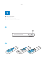
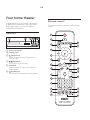
Home Theater DVD Player
HTS3531/12/51/94/98/F7/55/78/93
Service
Service Manual
TABLE OF CONTENTS
Page
. Location of PCB Boards&Version Variation&Repair Scenario Matrix..........1-2
. Technical Specifications…………....………………………..............1-3
. Safety Instruction, Warning & Notes….……………………....….....1-4
. DFU Instruction..............................................................................2-1
. Mechanical and Dismantling Instructions…………........................3-1
. Software Upgrades ........................................................................4-1
. Change settings.......................................…………........................4-2
. Trouble Shooting Chart………………………………………………. 5-1
. Wiring Diagram………………………………………..………..….….6-1
. Electrical Diagrams and Print-layouts..….…………………....….…7-1
. Set Mechanical Exploded view & Part list.…………………..….….8-1
. Revision List..................................................................................9-1
©Copyright 2011 Philips Consumer Electronics B.V. Eindhoven, The Netherlands
All rights reserved. No part of this publication may be reproduced, stored in aretrieval system or
transmitted, in any form or by any means, electronic, mechanical, photocopying, or otherwise
without the prior permission of Philips.
Published by RY&LLL - 1147 BU AVM Printed in The Netherlands Subject to modification
Version 1.3
CLASS 1
LASER PRODUCT
GB
3139 785 35843
PHILIPS
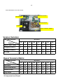
1-2
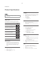
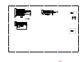
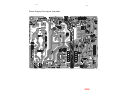
PCB BOARD LOCATION:
AMPLIFIER BOARD
MAIN BOARD
POWER BOARD
LOADER
FRONT CONTROL BOARD
Version Variation
Type/Versions
HTS3531
/12
/51
/94
/98
/F7
/55
/78
/93
Output Power- 300W
X
X
X
X
X
X
X
X
Voltage(220~240V~)
X
X
X
Features
Voltage(110~240V~)
MP3 LINK
X
X
X
X
X
X
X
X
X
X
X
X
X
Repair Scenario Matrix
Type/Versions
HTS3531
/12
/51
/94
/98
/F7
/55
/78
/93
Main Board
B
B
C
C
C
C
C
C
Front Control Board
B
B
C
C
C
C
C
C
Amplifier Board
B
B
C
C
C
C
C
C
Power Board
B
B
C
C
C
C
C
C
Board in used
*Bd:Board Level Replacement
*C:Component Level Repair
1-3
HTS3531/12/55/78:
Product Specifications:
Amplifier
Note
• Specifications and design are subject to change
without notice.
•
•
•
Region codes
•
The type plate on the back or bottom of the
home theater shows which regions it supports.
Country
DVD
Europe, United Kingdom
Total output power: 300W RMS (30%
THD)
Frequency response: 20 Hz-20 kHz / ±3 dB
Signal-to-noise ratio: > 65 dB (CCIR) /
(A-weighted)
Input sensitivity:
• AUX: 2 V
• Music iLink: 1 V
Video
•
•
Signal system: PAL / NTSC
HDMI output: 480i/576i, 480p/576p, 720p,
1080i, 1080p
Asia Pacific, Taiwan, Korea
Audio
Latin America
•
•
Australia, New Zealand
•
Russia, India
China
Radio
•
Media formats
•
DVD-Video, DVD+R/+RW, DVD-R/-RW,
DVD+R/-R DL, CD-R/CD-RW, Audio CD,
Video CD/SVCD, Picture files, MP3 media,
WMA media, DivX media, USB storage
device
File formats
•
•
•
Audio: .mp3, .wma
Video: .avi, .divx, .mpg, .mpeg,
Picture: .jpg, .jpeg
S/PDIF Digital audio input:
• Optical: TOSLINK
Sampling frequency:
• MP3: 32 kHz, 44.1 kHz, 48 kHz
• WMA: 44.1 kHz, 48 kHz
Constant bit rate:
• MP3: 32 kbps - 320 kbps
• WMA: 64 kbps - 192 kbps
•
•
Tuning range:
• Europe/Russia/China: FM 87.5-108
MHz (50 kHz)
• Asia Pacific/Latin America: FM 87.5-108
MHz (50/100 kHz)
Signal-to-noise ratio: FM 50 dB
Frequency response: FM 200 Hz-12.5 kHz
/ ±6 dB
USB
•
•
•
•
Compatibility: Hi-Speed USB (2.0)
Class support: USB Mass Storage Class
(MSC)
File system: FAT16, FAT32
Maximum memory support: < 160 GB
1-4
Main unit
•
•
•
•
•
Power supply:
• Europe/China/Russia/India: 220-240V,
~50 Hz
• Latin America/Asia Pacific: 110-240V
~50-60 Hz
Power consumption: 55 W
Standby power consumption: 0.9 W
Dimensions (WxHxD): 360 x 58 x 325 mm
Weight: 2.3 kg
Subwoofer
•
•
•
•
•
•
Output power: 50 W RMS (30% THD)
Impedance: 4 ohm
Speaker drivers: 133 mm (5.25”) woofer
Dimensions (WxHxD): 160 x 265 x 265 mm
Weight: 2.5 kg
Cable length: 3 m
Speakers
Center speaker:
Output power: 50 W RMS (30% THD)
System: 1 x 63.5 mm (2.5”) full range
Speaker impedance: 4 ohm
Speaker drivers: 1 x 63.5 mm (2.5”) woofer
Dimensions (WxHxD): 159 x 84.5 x 80 mm
Weight: 0.35 kg
Cable length: 2 m
Front/Rear speaker:
• Output power: 4 x 50 W RMS (30% THD)
• Speaker impedance: 4 ohm
• Speaker drivers: 1 x 63.5 mm (2.5”) full range
• Dimensions (WxHxD): 84.5 x159 x 80mm
• Weight (front): 0.35 kg/each
• Weight (rear): 0.35 kg/each
• Cable length (front): 4 m
• Cable length (rear): 10 m
•
•
•
•
•
•
•
Remote control batteries
•
2 x AAA-R03-1.5 V
Laser
•
•
•
•
Type: Semiconductor laser GaAIAs (CD)
Wave length: 645 - 665 nm (DVD), 770 800 nm (CD)
Output power: 6 mW (DVD), 7 mW
(VCD/CD)
Beam divergence: 60 degrees.
1-5
HTS3531/51
Amplifier
Product Specifications:
•
•
•
Note
•
• Specifications and design are subject to change
without notice.
Total output power: 300W RMS (30%
THD)
Frequency response: 20 Hz-20 kHz / ±3 dB
Signal-to-noise ratio: > 65 dB (CCIR) /
(A-weighted)
Input sensitivity:
• AUX: 2 V
• Music iLink: 1 V
Video
Region codes
The type plate on the back or bottom of the
home theater shows which regions it supports.
Country
DVD
Europe, United Kingdom
•
•
Audio
•
•
Asia Pacific, Taiwan, Korea
•
Latin America
Australia, New Zealand
S/PDIF Digital audio input:
• Optical: TOSLINK
Sampling frequency:
• MP3: 32 kHz, 44.1 kHz, 48 kHz
• WMA: 44.1 kHz, 48 kHz
Constant bit rate:
• MP3: 32 kbps - 320 kbps
• WMA: 64 kbps - 192 kbps
Radio
•
Russia, India
China
Signal system: PAL / NTSC
HDMI output: 480i/576i, 480p/576p, 720p,
1080i, 1080p
•
•
Tuning range:
• Europe/Russia/China: FM 87.5-108
MHz (50 kHz)
• Asia Pacific/Latin America: FM 87.5-108
MHz (50/100 kHz)
Signal-to-noise ratio: FM 50 dB
Frequency response: FM 200 Hz-12.5 kHz
/ ±6 dB
Media formats
USB
•
•
•
•
•
DVD-Video, DVD+R/+RW, DVD-R/-RW,
DVD+R/-R DL, CD-R/CD-RW, Audio CD,
Video CD/SVCD, Picture files, MP3 media,
WMA media, DivX media, USB storage
device
File formats
•
•
•
Audio: .mp3, .wma
Video: .avi, .divx, .mpg, .mpeg,
Picture: .jpg, .jpeg
Compatibility: Hi-Speed USB (2.0)
Class support: USB Mass Storage Class (MSC)
File system: FAT16, FAT32
Maximum memory support: < 160 GB
1-6
Main unit
•
Power supply:
Europe/China/Russia/India: 220-240V,
~50 Hz
• Latin America/Asia Pacific: 110-240V
~50-60 Hz
Power consumption: 55 W
Standby power consumption: 0.9 W
Dimensions (WxHxD): 360 x 58 x 325 mm
Weight: 2.3 kg
•
•
•
•
•
Subwoofer
•
•
•
•
•
•
Output power: 50 W RMS (30% THD)
Impedance: 4 ohm
Speaker drivers: 133 mm (5.25”) woofer
Dimensions (WxHxD): 160 x 265 x 265 mm
Weight: 2.5 kg
Cable length: 3 m
Speakers
Center speaker:
Output power: 50 W RMS (30% THD)
System: 1 x 63.5 mm (2.5”) full range
Speaker impedance: 4 ohm
Speaker drivers: 1 x 63.5 mm (2.5”) woofer
Dimensions (WxHxD): 159 x 84.5 x 80 mm
Weight: 0.35 kg
Cable length: 2 m
Front/Rear speaker:
• Output power: 4 x 50 W RMS (30% THD)
• Speaker impedance: 4 ohm
• Speaker drivers: 1 x 63.5 mm (2.5”) full range
• Dimensions (WxHxD): 84.5 x159 x 80mm
• Weight (front): 0.35 kg/each
• Weight (rear): 0.35 kg/each
• Cable length (front): 4 m
• Cable length (rear): 10 m
•
•
•
•
•
•
•
Remote control batteries
•
2 x AAA-R03-1.5 V
Laser
•
•
•
•
Type: Semiconductor laser GaAIAs (CD)
Wave length: 645 - 665 nm (DVD), 770 800 nm (CD)
Output power: 6 mW (DVD), 7 mW
(VCD/CD)
Beam divergence: 60 degrees.
1-7
HTS3531/94
Amplifier
Product Specifications:
Note
•
•
•
•
• Specifications and design are subject to change
without notice.
Total output power: 300W RMS (30%
THD)
Frequency response: 20 Hz-20 kHz / ±3 dB
Signal-to-noise ratio: > 65 dB (CCIR) /
(A-weighted)
Input sensitivity:
• AUX: 2 V
• Music iLink: 1 V
Video
Region codes
The type plate on the back or bottom of the
home theater shows which regions it supports.
Country
DVD
Europe, United Kingdom
•
•
Audio
•
•
Asia Pacific, Taiwan, Korea
•
Latin America
Australia, New Zealand
S/PDIF Digital audio input:
• Optical: TOSLINK
Sampling frequency:
• MP3: 32 kHz, 44.1 kHz, 48 kHz
• WMA: 44.1 kHz, 48 kHz
Constant bit rate:
• MP3: 32 kbps - 320 kbps
• WMA: 64 kbps - 192 kbps
Radio
•
Russia, India
China
Signal system: PAL / NTSC
HDMI output: 480i/576i, 480p/576p, 720p,
1080i, 1080p
•
•
Tuning range:
• Europe/Russia/China: FM 87.5-108
MHz (50 kHz)
• Asia Pacific/Latin America: FM 87.5-108
MHz (50/100 kHz)
Signal-to-noise ratio: FM 50 dB
Frequency response: FM 200 Hz-12.5 kHz
/ ±6 dB
Media formats
USB
•
•
•
DVD-Video, DVD+R/+RW, DVD-R/-RW,
DVD+R/-R DL, CD-R/CD-RW, Audio CD,
Video CD/SVCD, Picture files, MP3 media,
WMA media, DivX media, USB storage
device
File formats
•
•
•
Audio: .mp3, .wma
Video: .avi, .divx, .mpg, .mpeg,
Picture: .jpg, .jpeg
•
•
Compatibility: Hi-Speed USB (2.0)
Class support: USB Mass Storage Class
(MSC)
File system: FAT16, FAT32
Maximum memory support: < 160 GB
1-8
Main unit
•
Power supply:
Europe/China/Russia/India: 220-240V,
~50 Hz
• Latin America/Asia Pacific: 110-240V
~50-60 Hz
Power consumption: 55 W
Standby power consumption: 0.9 W
Dimensions (WxHxD): 360 x 58 x 325 mm
Weight: 2.3 kg
•
•
•
•
•
Subwoofer
•
•
•
•
•
•
Output power: 50 W RMS (30% THD)
Impedance: 4 ohm
Speaker drivers: 133 mm (5.25”) woofer
Dimensions (WxHxD): 160 x 265 x 265 mm
Weight: 2.5 kg
Cable length: 3 m
Speakers
Center speaker:
Output power: 50 W RMS (30% THD)
System: 1 x 63.5 mm (2.5”) full range
Speaker impedance: 4 ohm
Speaker drivers: 1 x 63.5 mm (2.5”) woofer
Dimensions (WxHxD): 159 x 84.5 x 80 mm
Weight: 0.35 kg
Cable length: 2 m
Front/Rear speaker:
• Output power: 4 x 50 W RMS (30% THD)
• Speaker impedance: 4 ohm
• Speaker drivers: 1 x 63.5 mm (2.5”) full range
• Dimensions (WxHxD): 84.5 x159 x 80mm
• Weight (front): 0.35 kg/each
• Weight (rear): 0.35 kg/each
• Cable length (front): 4 m
• Cable length (rear): 10 m
•
•
•
•
•
•
•
Remote control batteries
•
2 x AAA-R03-1.5 V
Laser
•
•
•
•
Type: Semiconductor laser GaAIAs (CD)
Wave length: 645 - 665 nm (DVD), 770 800 nm (CD)
Output power: 6 mW (DVD), 7 mW
(VCD/CD)
Beam divergence: 60 degrees.
1-9
HTS3531/98
Product Specifications:
Amplifier
Note
• Specifications and design are subject to change
without notice.
•
•
•
•
Region codes
The type plate on the back or bottom of the
home theater shows which regions it supports.
Country
DVD
Europe, United Kingdom
Total output power: 300W RMS (30%
THD)
Frequency response: 20 Hz-20 kHz / ±3 dB
Signal-to-noise ratio: > 65 dB (CCIR) /
(A-weighted)
Input sensitivity:
• AUX: 2 V
• Music iLink: 1 V
Video
•
•
Signal system: PAL / NTSC
HDMI output: 480i/576i, 480p/576p, 720p,
1080i, 1080p
Asia Pacific, Taiwan, Korea
Audio
Latin America
•
•
Australia, New Zealand
•
Russia, India
China
Radio
•
Media formats
•
DVD-Video, DVD+R/+RW, DVD-R/-RW,
DVD+R/-R DL, CD-R/CD-RW, Audio CD,
Video CD/SVCD, Picture files, MP3 media,
WMA media, DivX media, USB storage
device
File formats
•
•
•
Audio: .mp3, .wma
Video: .avi, .divx, .mpg, .mpeg,
Picture: .jpg, .jpeg
S/PDIF Digital audio input:
• Optical: TOSLINK
Sampling frequency:
• MP3: 32 kHz, 44.1 kHz, 48 kHz
• WMA: 44.1 kHz, 48 kHz
Constant bit rate:
• MP3: 32 kbps - 320 kbps
• WMA: 64 kbps - 192 kbps
•
•
Tuning range:
• Europe/Russia/China: FM 87.5-108
MHz (50 kHz)
• Asia Pacific/Latin America: FM 87.5-108
MHz (50/100 kHz)
Signal-to-noise ratio: FM 50 dB
Frequency response: FM 200 Hz-12.5 kHz
/ ±6 dB
USB
•
•
•
•
Compatibility: Hi-Speed USB (2.0)
Class support: USB Mass Storage Class
(MSC)
File system: FAT16, FAT32
Maximum memory support: < 160 GB
1-10
Main unit
•
Power supply:
Europe/China/Russia/India: 220-240V,
~50 Hz
• Latin America/Asia Pacific: 110-240V
~50-60 Hz
Power consumption: 55 W
Standby power consumption: 0.9 W
Dimensions (WxHxD): 360 x 58 x 325 mm
Weight: 2.3 kg
•
•
•
•
•
Subwoofer
•
•
•
•
•
•
Output power: 50 W RMS (30% THD)
Impedance: 4 ohm
Speaker drivers: 133 mm (5.25”) woofer
Dimensions (WxHxD): 160 x 265 x 265 mm
Weight: 2.5 kg
Cable length: 3 m
Speakers
Center speaker:
• Output power: 50 W RMS (30% THD)
• System: 1 x 63.5 mm (2.5”) full range
• Speaker impedance: 4 ohm
• Speaker drivers: 1 x 63.5 mm (2.5”) woofer
• Dimensions (WxHxD): 159 x 84.5 x 80 mm
• Weight: 0.35 kg
• Cable length: 2 m
Front/Rear speaker:
• Output power: 4 x 50 W RMS (30% THD)
• Speaker impedance: 4 ohm
• Speaker drivers: 1 x 63.5 mm (2.5”) full range
• Dimensions (WxHxD): 84.5 x159 x 80mm
• Weight (front): 0.35 kg/each
• Weight (rear): 0.35 kg/each
• Cable length (front): 4 m
• Cable length (rear): 10 m
Remote control batteries
•
2 x AAA-R03-1.5 V
Laser
•
•
•
•
Type: Semiconductor laser GaAIAs (CD)
Wave length: 645 - 665 nm (DVD), 770 800 nm (CD)
Output power: 6 mW (DVD), 7 mW
(VCD/CD)
Beam divergence: 60 degrees.
1-11
HTS3531/F7
Product Specifications:
Amplifier
Note
• Specifications and design are subject to change
without notice.
•
•
•
Region codes
•
The type plate on the back or bottom of the
home theater shows which regions it supports.
Country
DVD
Europe, United Kingdom
Total output power: 300W RMS (30%
THD)
Frequency response: 20 Hz-20 kHz / ±3 dB
Signal-to-noise ratio: > 65 dB (CCIR) /
(A-weighted)
Input sensitivity:
• AUX: 2 V
• Music iLink: 1 V
Video
•
•
Signal system: PAL / NTSC
HDMI output: 480i/576i, 480p/576p, 720p,
1080i, 1080p
Asia Pacific, Taiwan, Korea
Audio
Latin America
•
•
Australia, New Zealand
•
Russia, India
China
Radio
•
Media formats
•
DVD-Video, DVD+R/+RW, DVD-R/-RW,
DVD+R/-R DL, CD-R/CD-RW, Audio CD,
Video CD/SVCD, Picture files, MP3 media,
WMA media, DivX media, USB storage
device
File formats
•
•
•
Audio: .mp3, .wma
Video: .avi, .divx, .mpg, .mpeg,
Picture: .jpg, .jpeg
S/PDIF Digital audio input:
• Optical: TOSLINK
Sampling frequency:
• MP3: 32 kHz, 44.1 kHz, 48 kHz
• WMA: 44.1 kHz, 48 kHz
Constant bit rate:
• MP3: 32 kbps - 320 kbps
• WMA: 64 kbps - 192 kbps
•
•
Tuning range:
• Europe/Russia/China: FM 87.5-108
MHz (50 kHz)
• Asia Pacific/Latin America: FM 87.5-108
MHz (50/100 kHz)
Signal-to-noise ratio: FM 50 dB
Frequency response: FM 200 Hz-12.5 kHz
/ ±6 dB
USB
•
•
•
•
Compatibility: Hi-Speed USB (2.0)
Class support: USB Mass Storage Class
(MSC)
File system: FAT16, FAT32
Maximum memory support: < 160 GB
1-12
Main unit
•
•
•
•
•
Power supply:
• Europe/China/Russia/India: 220-240V,
~50 Hz
• Latin America/Asia Pacific: 110-240V
~50-60 Hz
Power consumption: 60W
Standby power consumption: 0.9 W
Dimensions (WxHxD): 360 x 58 x 325 mm
Weight: 2.3 kg
Subwoofer
•
•
•
•
•
•
Output power: 50 W RMS (30% THD)
Impedance: 4 ohm
Speaker drivers: 133 mm (5.25”) woofer
Dimensions (WxHxD): 160 x 265 x 265 mm
Weight: 2.5 kg
Cable length: 3 m
Speakers
Center speaker:
Output power: 50 W RMS (30% THD)
System: 1 x 63.5 mm (2.5”) full range
Speaker impedance: 4 ohm
Speaker drivers: 1 x 63.5 mm (2.5”) woofer
Dimensions (WxHxD): 159 x 84.5 x 80 mm
Weight: 0.35 kg
Cable length: 2 m
Front/Rear speaker:
• Output power: 4 x 50 W RMS (30% THD)
• Speaker impedance: 4 ohm
• Speaker drivers: 1 x 63.5 mm (2.5”) full range
• Dimensions (WxHxD): 84.5 x159 x 80mm
• Weight (front): 0.35 kg/each
• Weight (rear): 0.35 kg/each
• Cable length (front): 4 m
• Cable length (rear): 10 m
•
•
•
•
•
•
•
Remote control batteries
•
2 x AAA-R03-1.5 V
Laser
•
•
•
•
Type: Semiconductor laser GaAIAs (CD)
Wave length: 645 - 665 nm (DVD), 770 800 nm (CD)
Output power: 6 mW (DVD), 7 mW
(VCD/CD)
Beam divergence: 60 degrees.
1-13
HTS3531/93
Product Specifications:
Amplifier
Note
• Specifications and design are subject to change
•
•
•
without notice.
•
Total output power: 300W RMS (30% THD)
Frequency response: 20 Hz-20 kHz / ±3 dB
Signal-to-noise ratio: > 65 dB (CCIR) /
(A-weighted)
Input sensitivity:
• AUX: 2 V
• Music iLink: 1 V
Region codes
The type plate on the back or bottom of the
home theater shows which regions it supports.
Country
DVD
Video
•
•
Signal system: PAL / NTSC
HDMI output: 480i/576i, 480p/576p, 720p,
1080i, 1080p
Europe, United Kingdom
Audio
Asia Pacific, Taiwan, Korea
Latin America
•
•
•
Australia, New Zealand
Russia, India
China
Media formats
•
DVD-Video, DVD+R/+RW, DVD-R/-RW,
DVD+R/-R DL, CD-R/CD-RW, Audio CD,
Video CD/SVCD, Picture files, MP3 media,
WMA media, DivX media, USB storage
device
File formats
•
•
•
Audio: .mp3, .wma
Video: .avi, .divx, .mpg, .mpeg,
Picture: .jpg, .jpeg
S/PDIF Digital audio input:
• Optical: TOSLINK
Sampling frequency:
• MP3: 32 kHz, 44.1 kHz, 48 kHz
• WMA: 44.1 kHz, 48 kHz
Constant bit rate:
• MP3: 32 kbps - 320 kbps
• WMA: 64 kbps - 192 kbps
Radio
•
•
•
Tuning range:
• Europe/Russia/China: FM 87.5-108 MHz
(50 kHz)
• Asia Pacific/Latin America: FM 87.5-108
MHz (50/100 kHz)
Signal-to-noise ratio: FM 50 dB
Frequency response: FM 200 Hz-12.5 kHz /
±6 dB
USB
•
•
•
•
Compatibility: Hi-Speed USB (2.0)
Class support: USB Mass Storage Class
(MSC)
File system: FAT16, FAT32
Maximum memory support: < 160 GB
1-14
Main unit
•
•
•
•
•
Power supply:
• Europe/China/Russia/India: 220-240V~,
50 Hz
• Latin America/Asia Pacific: 110-240V~,
50-60 Hz
Power consumption: W
Standby power consumption: 0.9 W
Dimensions (WxHxD): 360 x 58 x 325 mm
Weight: 2.3 kg
Subwoofer
•
•
•
•
•
•
Output power: 50 W RMS (30% THD)
Impedance: 4 ohm
Speaker drivers: 133 mm (5.25") woofer
Dimensions (WxHxD): 160 x 265 x 265 mm
Weight: 2.50 kg
Cable length: 3 m
Speakers
Center speaker:
Output power: 50 W RMS (30% THD)
System: 1 x 63.5 mm (2.5") full range
Speaker impedance: 4 ohm
Speaker drivers: 1 x 63.5 mm (2.5") woofer
Dimensions (WxHxD): 159 x 84.5 x 80 mm
Weight: 0.35 kg
Cable length: 2 m
Front/Rear speaker:
• Output power: 4 x 50 W RMS (30% THD)
• Speaker impedance: 4 ohm
• Speaker drivers: 1 x 63.5 mm (2.5") full range
• Dimensions (WxHxD): 84.5 x159 x 80mm
• Weight (front): 0.35 kg/each
• Weight (rear): 0.35 kg/each
• Cable length (front): 3 m
• Cable length (rear): 7 m
•
•
•
•
•
•
•
Remote control batteries
•
2 x AAA-R03-1.5 V
Laser
•
•
•
•
Type: Semiconductor laser GaAIAs (CD)
Wave length: 645 - 665 nm (DVD), 770 - 800
nm (CD)
Output power: 6 mW (DVD), 7 mW (VCD/
CD)
Beam divergence: 60 degrees.
1-15
Safety instruction, Warning & Notes
Safety instruction
1. General safety
2.Laser safety
Safety regulations require that during a repair:
. Connect the unit to the mains via an isolation transformer.
. Replace safety components indicated by the symbol
,
only by components identical to the original ones. Any
other component substitution (other than original type)
may increase risk of fire or electrical shock hazard.
Safety regulations require that after a repair, you must
return the unit in its original condition. Pay, in particular,
attention to the following points:
. Route the wires/cables correctly, and fix them with the
mounted cable clamps.
. Check the insulation of the mains lead for external
damage.
. Check the electrical DC resistance between the mains
plug and the secondary side:
1) Unplug the mains cord, and connect a wire between
the two pins of the mains plug.
2) Set the mains switch the “on” position (keep the
mains cord unplug).
3)
Measure the resistance value between the mains
plug and the front panel, controls, and chassis
bottom.
4)
Repair
or
correct
unit
when
¡
measurement is less than 1M
the
resistance
.
5) Verify this, before you return the unit to the
customer/user (ref. UL-standard no. 1492).
6) Switch the unit “off”, and remove the wire between
the two pins of the mains plug.
This unit employs a laser. Only qualified service personnel
may remove the cover, or attempt to service this device
(due to possible eye injury).
Laser device unit
Type
: Semiconductor laser GaAlAs
Wavelength
: 650nm (DVD)
: 780nm (VCD/CD)
Output power
: 7mW (DVD)
: 10mW (DVD /CD)
Beam divergence: 60 degree
Note: Use of controls or adjustments or performance of
procedure other than those specified herein, may result in
hazardous radiation exposure. Avoid direct exposure to
beam.
1-16
Warning
1.General
2. Laser
. All ICs and many other semiconductors are susceptible to
. The use of optical instruments with this product, will
electrostatic discharges (ESD). Careless handing during
increase eye hazard.
repair can reduce life drastically. Make sure that, during
. Only qualified service personnel may remove the cover
repair, you are at the same potential as the mass of the
or attempt to service this device, due to possible eye
set by a wristband with resistance. Keep components and
injury.
tools at this same potential. Available ESD protection
with a disc loaded inside the player.
equipment:
1)
. Repair handing should take place as much as possible
Complete kit ESD3 (small tablemat, wristband,
connection box, extension cable and earth cable)
. Text below is placed inside the unit, on the laser cover
shield:
4822 310 10671.
2)
Wristband tester 4822 344 13999.
. Be careful during measurements in the live voltage
section. The primary side of the power supply , including
the heat sink, carries live mains voltage when you
CAUTION: VISIBLE AND INVISIBLE LASER
RADIATION WHEN OPEN, AVOID EXPOSURE
TO BEAM.
connect the player to the mains (even when the player is
“off”!). It is possible to touch copper tracks and/or
components in this unshielded primary area, when you
Notes:
service
Laboratories. The double-D symbol is trademarks of Dolby
the
player.
Service
personnel
must
take
precautions to prevent touching this area or components
in this area. A “lighting stroke” and a stripe-marked
printing on the printed wiring board, indicate the primary
side of the power supply.
. Never replace modules, or components, while the unit is
“on”.
Manufactured
under
licence
Laboratories, Inc. All rights reserved.
from
Dolby
1-17
6HUYLFH+LQWV
&$87,21
&+$5*('&$3$&,7256217+(6(592%2$5'0$<'$0$*(7+('5,9(
(/(&7521,&6:+(1&211(&7,1*$1(:'5,9(7+$7¶6:+<%(6,'(67+(6$)(7<
0($685(6/,.(
6:,7&+2))32:(56833/<
(6'3527(&7,21
$'',7,21$/$&7,2160867%(7$.(1%<7+(5(3$,57(&+1,&,$1
7KHIROORZLQJVWHSVKDYHWREHGRQHZKHQUHSODFLQJWKHGHIHFWLYHORDGHU
'LVPDQWOLQJRIWKHORDGHUWRDFFHVVWKH(6'SURWHFWLRQSRLQWLIQHFHVVDU\
6ROGHUWKH(6'SURWHFWLRQSRLQW 'LVFRQQHFWÀH[IRLOFDEOHIURPWKHGHIHFWLYHORDGHU
3XWDSDSHUFOLSRQWKHÀH[IRLOWRVKRUWFLUFXLWWKHFRQWDFWV¿J
5HSODFHWKHGHIHFWLYHORDGHUZLWKDQHZORDGHU
5HPRYHSDSHUFOLSIURPWKHÀH[IRLODQGFRQQHFWLWWRWKHQHZORDGHU
5HPRYHVROGHUMRLQWRQWKH(6'SURWHFWLRQSRLQW
$77(17,217KHODVHUGLRGHRIWKLVORDGHULVSURWHFWHGDJDLQVW(6'E\DVROGHUMRLQWZKLFKVKRUWFLUFXLWVWKHODVHUGLRGHWRJURXQG
)RUSURSHUIXQFWLRQDOLW\RIWKHORDGHUWKLVVROGHUMRLQWPXVWEHUHPRYHDIWHUFRQQHFWLRQORDGHUWRWKHVHW
Solder Joint
(6'SURWHFWLRQSRLQWLVDFFHVVLEOHIURPWRSRIORDGHU
2QO\DSSOLFDEOHIRUGHIHFWLYHORDGHUQHHGHGWREHVHQWEDFNWRVXSSOLHUIRUIDLOXUHDQDO\VLVDQGWRVXSSRUWEDFNFKDUJLQJ
HYLGHQFH
7KLVLVDOVRDSSOLFDEOHIRUDOOSDUWQHUVKLSZRUNVKRSV
1-18
Notes
Lead-Free requirement for service
INDENTIFICATION:
x
Regardless of special logo (not always indicated)
Use only original spare-parts listed in the
Service-Manuals. Not listed standard-material
(commodities) has to be purchased at external
One must treat all sets from 1.1.2005 onwards, according
next rules.
companies.
x
Important note: In fact also products a little older can also
be treated in this way as long as you avoid mixing
solder-alloys (leaded/ lead-free). So best to always use
SAC305 and the higher temperatures belong to this.
Special information for BGA-ICs:
- always use the 12nc-recognizable soldering
temperature profile of the specific BGA (for
de-soldering
always
use
highest
lead-free
temperature profile, in case of doubt)
Due to lead-free technology some rules have to be
respected by the workshop during a repair:
- lead free BGA-ICs will be delivered in so-called
‘dry-packaging’ (sealed pack including a silica gel
x Use only lead-free solder alloy Philips SAC305 with
order code 0622 149 00106. If lead-free solder-paste is
pack) to protect the IC against moisture. After
required, please contact the manufacturer of your
opening, dependent of MSL-level seen on
solder-equipment. In general use of solder-paste within
indicator-label in the bag, the BGA-IC possibly
workshops should be avoided because paste is not easy
still
to store and to handle.
communicated via AYS-website.
to
be
baked
dry.
This
will
be
Do not re-use BGAs at all.
x Use only adequate solder tools applicable for lead-free
solder alloy. The solder tool must be able
has
x
For sets produced before 1.1.2005, containing
o To reach at least a solder-temperature of 400°C,
leaded soldering-tin and components, all needed
o To stabilize the adjusted temperature at the
spare-parts will be available till the end of the
solder-tip
o To exchange solder-tips for different applications.
x Adjust your solder tool so that a temperature around
360°C – 380°C is reached and stabilized at the solder
joint. Heating-time of the solder-joint should not exceed
service-period. For repair of such sets nothing
changes.
x On our website:
www.atyourservice.ce.Philips.com
You find more information to:
~ 4 sec. Avoid temperatures above 400°C otherwise
BGA-de-/soldering (+ baking instructions)
wear-out of tips will rise drastically and flux-fluid will be
Heating-profiles of BGAs and other ICs used in
destroyed. To avoid wear-out of tips switch off un-used
Philips-sets
equipment, or reduce heat.
x Mix of lead-free solder alloy / parts with leaded solder
alloy / parts is possible but PHILIPS recommends
You will find this and more technical information
within the “magazine”, chapter “workshop news”.
strongly to avoid mixed
For additional questions please contact your local
solder alloy types (leaded and lead-free). If one cannot
repair-helpdesk.
avoid, clean carefully the
solder-joint from old solder alloy and re-solder with new
solder alloy (SAC305).
2-1
EN Before using your product, read all accompanying safety
information
DA Læs alle medfølgende sikkerhedsoplysninger, inden du
tager produktet i brug
DE Lesen Sie vor Verwendung dieses Produkts alle
begleitenden Sicherheitsinformationen
EL ƑƱƩƭ ƷƱƧƳƩƬƯưƯƩƞƳƥƴƥ ƴƯ ưƱƯƺƼƭ, ƤƩơƢƜƳƴƥ ƼƫƥƲ ƴƩƲ
ươƱƥƷƼƬƥƭƥƲ ưƫƧƱƯƶƯƱƟƥƲ ơƳƶƜƫƥƩơƲ
ES Antes de usar el producto, lea toda la información de
seguridad adjunta
FI Lue kaikki turvallisuustiedot ennen tuotteen käyttöä
FR Avant d’utiliser votre produit, lisez l’intégralité des
consignes de sécurité jointes
IT Prima di utilizzare il prodotto, leggere tutte le relative
informazioni sulla sicurezza
NL Lees voordat u het product gaat gebruiken eerst alle
bijbehorende veiligheidsinformatie
NO Les all vedlagt sikkerhetsinformasjon før du bruker
produktet
PT Antes de utilizar o produto, leia todas as informações de
segurança que o acompanham
SV Innan du använder produkten ska du läsa all tillhörande
säkerhetsinformation
TR Ürününüzü kullanmadan önce ilgili tüm güvenlik bilgilerini
okuyun
CS Pŏed použitím produktu si pŏeĈtĖte doprovodné
bezpeĈnostní informace
HU A termék használata elʼntt alaposan olvassa el a mellékelt
biztonsági tudnivalókat
PL Przed rozpoczĔciem korzystania z produktu naleůy
zapoznaĂ siĔ z informacjami dotyczĀcymi bezpieczeļstwa
RO Înainte de a utiliza acest produs, citiŗi toate informaŗiile de
siguranŗþ care îl însoŗesc
SK Pred použitím produktu si preĈítajte všetky sprievodné
bezpeĈnostné informácie
User manual
India only
2-2
1
EN
HI
RU
UK
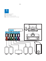
Connect the home theater
° ¤v |° |¬|² |¬j
ǜǻDZǷǸȋȄǵǿDz DZǻǹǭȅǺǵǶ ǷǵǺǻǿDzǭǿǽ
ǜȒDZ’ȐDZǺǭǺǺȌ ǾǵǾǿDzǹǵ DZǻǹǭȅǺȉǻǰǻ ǷȒǺǻǿDzǭǿǽȀ
SUB
WOOFER
FRONT
LEFT
FRONT
CENTER
FRONT
RIGHT
FRONT FRONT FRONT REAR REAR SUB
RIGHT LEFT CENTER RIGHT LEFT WOOFER
REAR
LEFT
FRONT
RIGHT
FRONT
LEFT
FRONT
CENTER
REAR
RIGHT
REAR
LEFT
REAR
RIGHT
SUB
WOOFER
2-3
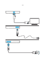
HDMI OUT
HDMI IN
)0
ANTENNA
AC MAINS~
2-4
X
2
EN
HI
RU
UK
1
2
Switch on the home theater
° ¤v |° ²¤ x |¬j
ǏǷǸȋȄǵǿDz DZǻǹǭȅǺǵǶ ǷǵǺǻǿDzǭǿǽ
ǠǯȒǹǷǺDzǺǺȌ ǾǵǾǿDzǹǵ DZǻǹǭȅǺȉǻǰǻ ǷȒǺǻǿDzǭǿǽȀ
2-5
3
EN
HI
RU
UK
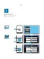
Complete the first time setup
¥ £ |¬ ¬l |° §² |¬j
ǏȈǼǻǸǺǵǿDz ǼDzǽǯǻǺǭȄǭǸȉǺȀȋ ǺǭǾǿǽǻǶǷȀ
ǏǵǷǻǺǭǺǺȌ ǼDzǽȅǵȂ ǺǭǸǭȅǿȀǯǭǺȉ
HDMI
1
TV
*HQHUDO6HWXS
2
(DV\/LQN6HWXS
'LVF/RFN
'LVSOD\'LP
26'/DQJXDJH
6FUHHQ6DYHU
6OHHS7LPHU
3
$XWR6WDQGE\
HOME THEATER
'LY;592'&RGH
*HQHUDO6HWXS
4
(DV\/LQN6HWXS
(QJOLVK
'LVF/RFN
Русский
'LVSOD\'LP
Українська
26'/DQJXDJH
6FUHHQ6DYHU
5
6OHHS7LPHU
$XWR6WDQGE\
HOME THEATER
'LY;592'&RGH
2-6
X
4
EN
HI
RU
UK
Use your home theater
l¬ ° ¤v |£ p°~ |¬j
ǑǻǹǭȅǺǵǶ ǷǵǺǻǿDzǭǿǽ ǰǻǿǻǯ Ƿ ǵǾǼǻǸȉǴǻǯǭǺǵȋ
ǏǵǷǻǽǵǾǿǭǺǺȌ ǾǵǾǿDzǹǵ DZǻǹǭȅǺȉǻǰǻ ǷȒǺǻǿDzǭǿǽȀ
1
3
2
1
2
2-7
1
MUSIC
iLINK
3
2
1
2
2-8
Your home theater
Remote control
Congratulations on your purchase, and welcome
to Philips! To fully benefit from the support that
Philips offers, register your home theater at
www.philips.com/welcome.
Main unit
This section includes an overview of the remote
control.
1
2
3
24
23
a Disc compartment
4
b Display panel
c
d
(Open/Close)
Open or close the disc compartment, or
eject the disc.
(Play/Pause)
Start, pause or resume play.
e SOURCE
Select an audio or video source for the
home theater.
f
(Standby-On)
Switch the home theater on or to standby.
5
6
22
21
7
8
20
19
9
18
10
11
12
17
13
16
14
15
2-9
a
(Standby-On)
Switch the home theater on or to
standby.
• When EasyLink is enabled, press
and hold for at least three seconds
to switch all connected HDMI CEC
compliant devices to standby.
•
b
(Open/Close)
Open or close the disc compartment, or
eject the disc.
c Source buttons
• DISC: Switch to disc source. Access
or exit the disc menu when you play
a disc.
AUDIO SOURCE : Select an audio
input source.
RADIO: Switch to FM radio.
USB : Switch to USB storage device.
•
•
•
d Navigation buttons
• Navigate menus.
• In video mode, press left or right to
fast backward or fast forward; press
up or down to slow backward or slow
forward.
In radio mode, press left or right to
search a radio station; press up or
down to fine tune a radio frequency.
•
e OK
Confirm an entry or selection.
f
BACK
Return to a previous menu screen.
g
/
•
•
h
(Previous/Next)
Skip to the previous or next track,
chapter or file.
In radio mode, select a preset radio
station.
(Mute)
Mute or restore volume.
i VOL +/Increase or decrease volume.
j SOUND
Select a sound mode.
k Numeric buttons
Select an item to play.
l ANGLE
Select video scenes recorded in different
camera angels.
m REPEAT / PROGRAM
• Select or turn off repeat mode.
• In radio mode, set a radio station.
n REPEAT A-B
Mark two points within a chapter or track
to repeat play, or turn off the repeat mode.
o CREATE MP3/ZOOM
• Access the create MP3 menu.
• Zoom into a video scene or picture.
Press the Navigation buttons (left/
right) to select a zoom factor.
p
SCREEN FIT
Fit the picture format to the TV screen.
q SUBTITLE
Select subtitle language for video.
r AUDIO SYNC
• Select an audio language or channel.
• Press and hold to access audio delay
setting, then press +/- to delay the
audio to match the video.
s SURR
Select surround sound or stereo sound.
t
(Stop)
Stop play.
u
(Play/Pause)
Start, pause or resume play.
v
INFO
Access more play options while playing a
disc or a USB storage device.
w
SETUP
Access or exit the setup menu.
x SLEEP
Switch the home theater to standby after a
specified time.
3-1
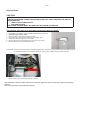
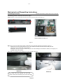
Mechanical and Dismantling Instructions
Dismantling Instruction
Detailed information please refer to the model set.
The following guidelines show how to dismantle the player.
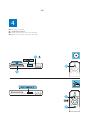
Step1: Remove 6 screws around the Top Cover, and then remove the Top Cover (Figure 1).
Sample Model:HTS3531/12
Figure 1
Step2: If it is necessary to dismantle Loader or Front Panel, the Front door should be removed first. (Figure 2)
Method A):Turn on the power button,then press open button to dismantle front door.Please kindly note that
power off as soon as front door is out of machine.
Method B): If the tray can’t open in normal way, you can make it through the instruction as below, an emergency eX it
at bottom cover of the machine.
Note: Make sure to operate gently otherwise the guider would be damaged.
Method A)
Method B)
Please kindly note that dismantle the front door
assembly carefully to avoid damage tray and the front door.
Figure 2
3-2
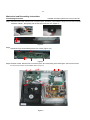
Mechanical and Dismantling Instructions
Detailed information please refer to the model set.
Dismantling Instruction
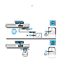
Step3 :Dismantle Front Panel, disconnect the connectors (XP4, XP8,XP12), need release 2 snaps of Front Panel & 2 snaps
of bottom cabinet , then gently pull the Panel out from the set. (Figure 3)
Figure 3
Step4 : Dismantle Front Control Board,remove 5 screws (Figure 4 /5)
Figure 4
Step5 : Dismantle Loader, disconnect the 3 connectors (XP2, XP3, XP6) aiming in the below figure, and remove 2 screws
that connects the loader and the bottom cabinet. (Figure 5)
Figure 5
3-3
Mechanical and Dismantling Instructions
Dismantling Instruction
Detailed information please refer to the model set.
Step6: Dismantle Main Board, first disconnect 2 connectors (XP1, XP11), and then remove 6 screws. (Figure 5/6)
Step7: Dismantle Power Board, disconnect the connectors XS703 and CN501 on Power Board,then remove 5 screws.(Figure 5/6)
Step8: Dismantle Amplifier Board, remove
4 screws (Figure 5/6)
XP8
XP4
XP11
XP701
XP3
XP2
XP1
XP6 XP12
XS703
CN501
Figure 6
4-1
Software Upgrade
1.Thereare2waystosoftwareupgrade:
First:
UpgradefromUSB:
CoppytheupgradefileHTS3531_XX.BINtoUSBthenpresstheUSB
keyonRCorSOURCEkeyonfrontpanel.
Whenupgradefiledetected,select"Yes"toupgrade,select"No"tocancel.
Afterupgradingbegins,amessage“DONOTPOWEROFF”willshow,orthe
productwillhangupandupgradingfailed.
Afteryoucancel,theproductwouldnotreadtheUSBunlessupgradefiledeleted.
Second:
UpgradefromDisc:
CoppytheupgradefileHTS3531_XX.BINtodiscthenreadthedisc.
Whenupgradefiledetected,select"Yes"toupgrade,select"No"tocancel.
After upgrading begins a message “DO
Afterupgradingbegins,amessage
DONOTPOWEROFF
NOT POWER OFF”willshow,orthe
will show or the
productwillhangupandupgradingfailed.
Afteryoucancel,theproductwouldnotreadDiscunlessupgradefiledeleted.
2.Checktheversioninformationafterupgraded.
PressthesetupkeyonRC,slectPreferenceSetup,andthenVersioninfo,press
OKKeyyouwillseeainterfacebelow:
How to adjust the setting after repairing:
1.HTS3531/12: Open DVD tray, press “9” “9” “9” “9” “2” on R/C;
2.HTS3531/51: Open DVD tray, press “9” “9” “9” “9” “5” on R/C;
3.HTS3531/94: Open DVD tray, press “9” “9” “9” “9” “5” on R/C;
4.HTS3531/55: Open DVD tray, press “9” “9” “9” “9” “4” on R/C;
5.HTS3531/98: Open DVD tray, press “9” “9” “9” “9” “3” on R/C;
6.HTS3531/F7: Open DVD tray, press “9” “9” “9” “9” “1” on R/C;
7.HTS3531/78: Open DVD tray, press “9” “9” “9” “9” “4” on R/C;
8.HTS3531/93: Open DVD tray, press “9” “9” “9” “9” “6” on R/C;
Note: Restart after above steps.
4-2
Change settings
This section helps you to change the settings of
your home theater.
Caution
0RVWRIWKHVHWWLQJVDUHDOUHDG\FRQÀJXUHGZLWKWKH
best value for your home theater. Unless you have a
reason to change a setting, it is best to leave it at the
default value.
Picture resolution
7RHQMR\KLJKGHÀQLWLRQ+'0,YLGHRRXWSXW
set the HDMI video settings that best match up
with your TV capability.
1
2
3
4
Press
-
.
Select [Video Setup], and then press OK.
Select [HDMI Setup], and then press OK.
Change the following settings, and then
press OK:
[Wide Screen Format]: For 16:9 wide
screen TV display setting.
[HDMI Video]: HDMI resolution.
Note
You cannot change a setting that is grayed out.
. To
To return to the previous menu, press
exit the menu, press
-
.
Change the picture settings to suit your
preferences.
Note
The best setting is automatically selected for the TV. If
you change the setting, make sure that the TV supports
the new settings.
Picture settings and format
Press
6XSSRUWKLJKGHÀQLWLRQ-3(*SLFWXUHV
1
2
3
Picture
1
2
3
+LJKGHÀQLWLRQSLFWXUH
-
.
Select [Video Setup], and then press OK.
Change the following settings, and then
press OK:
[TV System]: For TV supported video
format.
[TV Display]: For TV picture display
format.
[Picture Settings]3UHGHÀQHGFRORU
settings.
Press
-
.
Select [Video Setup], and then press OK.
Select [HD JPEG] > [On], and then press
OK.
Sound
Change the sound settings to suit your
preference.
HDMI audio
HDMI audio is automatically down-mixed to
two channel for TV speakers. If you do not want
to output audio through your TV, disable the
HDMI audio.
1
2
3
Press
-
.
Select [Audio Setup], and then press OK.
Select [HDMI Audio] > [Off], and then
press OK.
Language
Select a language for the home menu, audio,
and subtitles.
4-3
4
Home menu
1
2
Press
-
Select a menu language for discs, and then
press OK.
.
Select [General Setup], and then press
OK.
3
Select [OSD Language], and then press
OK.
4
Select a menu language for your home
theater, and then press OK.
Note
If your preferred disc language is not available, select
[Others] from the list, and enter the 4-digit language
code found at the end of this user manual.
If you select a language that is not available on a disc,
the home theater uses the default language of the disc.
Disc audio
Parental control
1
2
Press
Select [Preference Setup], and then press
OK.
Restrict access to discs.
3
4
Select [Audio], and then press OK.
Password
-
.
Select an audio language for discs, and then
press OK.
Note
If your preferred disc language is not available, select
[Others] from the list, and enter the 4-digit language
code found at the end of this user manual.
If you select a language that is not available on a disc,
the home theater uses the default language of the disc.
You can set or change your password to play a
restricted disc.
1
2
Press
3
Select [Password], and then press OK.
» A change password menu is displayed.
4
Follow the instructions on the TV to set or
change password.
If you do not have a password or you
have forgotten, enter 0000.
5
Press OK.
Disc subtitle
1
2
Press
3
4
Select [Subtitle], and then press OK.
-
.
Select [Preference Setup], and then press
OK.
Select a subtitle language for discs, and
then press OK.
Disc menu
1
2
Press
3
Select [Disc Menu], and then press OK.
-
.
Select [Preference Setup], and then press
OK.
Ratings
Some discs are recorded with ratings according
to age. You can set up your home theater to
play only discs with an age rating lower than
your child’s age.
1
2
Press
3
Select [Parental], and then press OK.
» A message prompts you to enter the
password.
.
Select [Preference Setup], and then press
OK.
-
-
.
Select [Preference Setup], and then press
OK.
4-4
4
Enter the password with the Numeric
buttons.
Sleep timer
5
Select an age rating, and then press OK.
To play all discs irrespective of the
rating, select level 8 or [Off].
Set timers to switch the home theater to
VWDQGE\DIWHUDVSHFLÀHGWLPH
Lock disc
To restrict access to discs that are not encoded
with ratings and parental control, lock the disc
manually. You can lock upto 20 discs on your
home theater.
1
2
3
4
While playing a disc, press
-
1
2
Press
3
4
Select [Sleep Timer], and then press OK.
5
Press OK to activate.
» The home theater switches to standby
DIWHUWKHVSHFLÀHGWLPH
.
Select [General Setup], and then press
OK.
Select [Disc Lock] > [Lock], and then
press OK.
» A message prompts you to enter the
password.
-
.
Select [General Setup], and then press
OK.
Select the duration of the sleep timer.
» The sleep timer can be set up to 60
minutes. If the sleep timer is set to
[Off], it switches off.
Screen saver
Enter the password with the Numeric
buttons.
» The disc is locked.
Automatically switch your home theater to
screen saver mode if:
it is in pause or stop mode, and
no button is pressed for 10 minutes.
To play the locked disc, enter the
password.
1
2
Press
3
Select [Screen Saver] > [On], and then
press OK.
Energy saving
-
.
Select [General Setup], and then press
OK.
Save energy by changing the following settings.
Display panel
Auto standby
When playing a disc or a USB storage device,
automatically switch your home theater to
standby if:
it is in pause or stop mode, and
no button is pressed for 30 minutes.
1
2
3
Press
-
.
Change the brightness of the home theater
display panel.
1
2
Press
3
4
Select [Display Dim], and then press OK.
-
.
Select [General Setup], and then press
OK.
Select the brightness, and then press OK.
Select [General Setup], and then press
OK.
Select [Auto Standby] > [On], and then
press OK.
Apply factory settings
Reset your home theater to the default settings.
You cannot reset the parental control settings.
4-5
1
2
Press
3
4
Select [Default], and then press OK.
-
.
Select [Preference Setup], and then press
OK.
Select [Ok], and then press OK.
EN
23
5-1
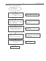
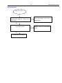
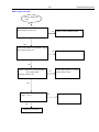
Trouble shooting Chart
VFD No display on Front Control Board
VFD No display on
Front Control Board
Go
Check every supply voltage on Main Board
whether normal or not.
(XP1 PIN1:-24V, PIN3: 12V, PIN5&PIN6:
5V)
No
Refer to CN502 on Power Board
Yes
Check voltage -24V, +5V, +12V on Power
No
Board at CN502 position and Front Control
Board
(HTS3531:XP2
PIN5:+12V
Fix the connection HTS3531:XP2 on
Front Control Board
PIN4:-24V
and
XP12 on
Main Board
PIN6:+3.3V)
Yes
Check the power key(HTS3531: S608),
open/closed key(HTS3531: K138), source
key(HTS3531: K135) on Touch Board
whether work normally or not
No
Replace U1 on Main Board, or replace
the Main Board
Yes
No
Check Front Control Board signals
SCL,SDA
(HTS3531:XP2 PIN8: SCL PIN7:SDA)
HTS3531:Check the U135 ON Front
Control Board pin 7 8 arrive the condition
XP8 PIN7 PIN8
Yes
Check whether bad solder exists on
HTS3531:XP8 on Front Control Board and
VFD135 of VFD,
Yes
Replace U135 or VFD
No
Correct connection
5-2
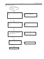
Trouble shooting Chart
keys do not work
keys do not work
Go
Check voltage +3.3V on Front Control Board
HTS3531:(XP2 PIN9) and voltage +5V on
U135 PIN14
No
HTS3531: Fix the connection XP2 on
Front Control Board
and
XP12 on
MAIN BOARD
Yes
Check Front Control Board signals (U135
PIN10,PIN11,PIN12)
No
Replace U135 on Front Control
Board
Yes
Replace Front Control Board
5-3
Trouble shooting Chart
Remote control does not work
Remote
control
does not work
Go
Check battery of remote control whether
Yes
exhausted or not.
Replace the battery for remote
control
No
Check power supply of IR601 on Front
Control Board whether normal or not
HTS3531:XP2 PIN9 3.3V
Yes
Replace IR601
No
Check the +3.3V net on Front
Control Board HTS3531:XP2
5-4
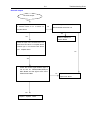
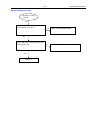
Trouble shooting Chart
No audio output
No audio output
Go
Check XP11 pin 14&16 3.3V on Main
Check voltage +34.5
V whether normal or not
at XP702 on
No
Board whether normal or not
Amplifier Board
Yes
Yes
Refer to CN502 on
Power Board
Check the 24pin FFC connection XP11 on
Main Board and XP701 on Amplifier Board
whether right or not between Main Board
and
Amplifier Board
No
Yes
Check the control signal whether right or
not at the U1 PIN59,PIN60,PIN63,on
Main Board and the signal at the XP11
PIN9 PIN10 PIN22
No
Replace U1 on Main Board,or
replace Main Board
Yes
Replace
Amplifier Board
5-5
Trouble shooting Chart
No video output
No video output
Go
Check L6 , R433 whether right on Main
No
Add
Board
Yes
Check the video signal whether
right at U1: PIN139
No
Replace Main Board
L6, R433 on Main Board
5-6
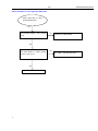
Trouble shooting Chart
Can’t read disc or can’t open the disk door
Can’t read disc or can’t
open the disk door
Go
work normally
No
Check 24pin 6pin and 5pin cable
from Main Board to Loader whether
connect right or not
No
Check loader whether
or not
Check XP1 on Main Board
Yes
Yes
Replace Loader
、
Fix 24pin 6pin and 5pin cable
5-7
Trouble shooting Chart
Tuner FM does not work
Tuner FM does not work
Go
Check voltage at Q6:+3.3V on Main
Board whether normal or not
No
Refer to Power Board CN502
Yes
Check voltage +3.3V
at Tuner
module (TUN1 pin5) whether right or
not
No
Check Main Board tuner power supply
circuit.
Yes
Check
Tuner
pin7,pin8,pin9,I2S output
normal or not
module
whether
No
Change the Tuner module
Yes
Check the U1 PIN53, PIN54. I2C
output on Main Board whether
normal or not
Yes
Replace Main Board
No
Check
Main
supply circuit
Board
U1
power
5-8
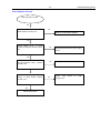
Trouble shooting Chart
AUX in does not work
AUX in does not
work
Go
Check voltage at U12 PIN8:12V on Main
Board whether normal or not
No
Refer to Power Board CN502
No
Check C166,C167,R87,R91
Yes
Check Main Board U5 PIN2,PIN15 signal
input whether right or not
Yes
Check voltage at U5 74HC4052 PIN16,
+6V, on Main Board
Whether normal or not
No
Check Main Board U1 power
supply and out circuit
Yes
Check U5 74HC4052
broken Or not
Yes
Replace U5 74HC4052
whether
No
Check Main Board U1
5-9
Trouble shooting Chart
MP3 Link does not work
MP3 Link does
not work
Go
HTS3531:Check signal at XS605:PIN3:MP3_R
PIN1:MP3_L ON front board whether normal
or not
No
Refer to Main Board XP8
No
Check Main Board C169, C170, R103,
Yes
Check Main Board U5 74HC4052
PIN4,PIN11 L/R signal input whether right
or not
R105,
Yes
Check voltage at U5 74HC4052
PIN16,VDD +6V, on Main Board
Whether normal or not
No
Check Main Board U1 power
supply and out circuit
Yes
Check U5 74HC4052 whether broken
Or not
No
Check Main Board U1
Yes
Replace U5 74HC4052
5-10
Trouble shooting Chart
OPTICAL IN does not work
OPTICAL in does
not work
Go
Check voltage at P2 PIN1:5V on Main
Board whether normal or not
No
Refer to Power Board CN502
Yes
Check Main Board P2 PIN3 signal input
whether right or not
Yes
Replace U1
No
Check Main Board C106,
6-1
6-1
4ohm
4ohm
SR
SL
SUB
FM TUNER
Optical Fiber
SR
1
6PIN
FL
IO 9pin
FLASH
I2C 2
AM5890
XP2
SHUTDOWN
AMP_DET
PDN
BKEN_ERR
XP701
Power limit
1
14PIN 1.0mm FFC
XP4
USB_DP
USB_DM
GND
VCC
GND
GND
MIC_DET
GND
-24V
+12V
3.3V
SCK
SDA
STB
GND
IR
PW_KEY
GND
GND
USB
MIC/MP3 IN
XP2
XS605
14PIN 1.0mm FFC
VFD DISPLAY+PT6312
XS604
1
XS703
+33V
+33V
6
+33V
PGND
PGND
PGND
1
8
8pin*2.5
GND
POWER_ON/OFF
5V
5V
GND
12V
GND
-24V
CN502
8PIN 2.5mm
5PIN2.0mm
XP12
MAIN BOARD
I2C 2
TJJ/MOS
Switch
AMP
XP1
XP6
IR 1pin
VFD&IO 10pin
P_CON 2pin
CN531
6PIN
POWER
SUPPLY
6
CN501
44
control circuit
CEN
AMP
STA309A
STA518
1
AMP
XP3
24
I2S_SD0
I2S_LRCK
I2S_SD1
I2S_SD2
I2S_BCLK
GND
I2S_MCLK
GND
SCL
SDA
GND
MUTE
DSP_RST
+3.3V
+12V
+3.3V
+12V
GND
GND
POWER
24PIN IDC
I2S 6pin
RDS DATA
I2C 1
6PIN2.0mm
ASA 8829+S76RFXP2
I2S 6pin
24PIN
0.5mm FFC
DVD LOADER
2PIN2.0mm
XP11
MT1389GH-FXE
AK5358
Audio process IC
4558
24PIN 0.5mm FFC
HC4052
88
STA518
SDRAM
132
LOADLOAD+
TRAYOUT
GND
TRAYIN
FR
SL
SUB WOOFER
10PIN2.0mm
SPSP+
LIMIT
GND
SLSL+
4ohm
HDMI
FAN
SPDIF
CVBS
RCA
Vc(Vref)
Vcc
E
NC
VR-CD
VR-DVD
CD-LD
MD
HFM
NC
DVD-LD
GND-LD
CEN
4ohm
FAN control
AUX L/R
FF+
T+
TC
D
CD/DVD SW
RF
A
B
F
GND-PD
4ohm
FL
4ohm
FR
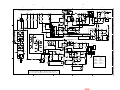
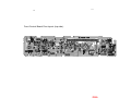
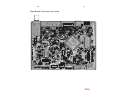
HTS3531 BLOCK / WIRING DIAGRAM
7-1
7-1
A
B
C
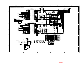
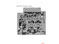
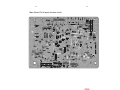
Front Control Board Circuit Diagram:
D
E
,
VFD
+12V
FB613
FB604
FB609
FB610
FB612
FB614
R142
F2
F2
NP
1G
2G
3G
4G
5G
6G
7G
8G
NC
P1
P2
P3
P4
P5
P6
P7
P8
P9
P10
P11
P12
P13
NC
P14
P15
NC
NP
F1
F1
1
2
3
4
5
6
7
8
9
10
11
12
13
14
15
16
17
18
19
20
21
22
23
24
25
26
27
28
29
30
31
32
C152
+3.3V
18K
0.1uF/50V/X7R
Q138
NPN_3DG3904M
4.7K
R143
Q139
CE138 3.3uF/50V
R136
2.2
R139
Q137
PNP_3CG3906M
R146
10K
R145
1K
NPN_3DG3904M
Q135
NPN_3DG3904M
R141
100
IR
IRM_12mm
ZD135
BZX79C6V2
R144
10K
CE135
3.3uF/50V
LR24
0
C135
1000pF/50V/X7R
-24V
33
32
31
30
29
28
27 LR24
26
25
24
23
C768
330
R147
1K
100pF/50V/NP0
C763
R140
R7
U135
+12V
R154
USB_DM
10K
+
CE606
0.1uF/16V/Y5V47uF/16V
3
2
R611
4
USB_VCC
R148
51K
C222
ZD136
C148
BZX79C5V1 4.7uF/16V/Y5V0.1uF/50V/X7R
+3.3V
USB_DP
G4
G3
G2
G1
VDD
LED4
LED3
LED2
LED1
GND
OSC
REM-3V3
10
1
34
35
36
37
38
39
40
41
42
43
44
+5VA
1K
ESD1
REM-3V3
R637
C617
C618
47pF/50V/NP0
AC2
+5V
6
Shell A Shell B
5
Q620
PNP_3CG3906M
R686
7.5K
R162
100
VSCLK
R163
100
VSTB
R164
100
P801
USB-A/BK
+5V
2.2K
+12V
VSDA
R9
0
R1
0
+5VA
C223
4.7uF/16V/Y5V
R161
4
3
2
1
4PIN/2.0mm/200mm
XS604
To main
board
10K
R683
2.2K
VCC
DD+
GND
USB_VCC 4
3
USB_DM 2
USB_DP 1
+5V
2.2K
R171
4.7K
R149
R159
10K
0
R684
750
01UUSBJAK-101
USB_VCC
USB_DM
USB_DP
1K
C774
NC/0.1uF/16V/Y5V
R150
R158
10K
R10
R157
10K
LED_RED
1
2
3
4
R165
2
LED1
PRTR5V0U2X
22
21
20
19
18
17
16
15
14
13
12
SEG8
SEG7
SEG6/K6
SEG5/K5
SEG4/K4
DRIVER_VFD_CS6312EN
SEG3/K3
SEG2/K2
SEG1/K1
VDD
KEY4
KEY3
SW1
SW2
SW3
SW4
SDout
SDin
GND
SCLK
/CS
KEY1
KEY2
1
2
3
4
5
100pF/50V/NP0
100pF/50V/NP0
100pF/50V/NP0
C769
C764
C766
C767
100pF/50V/NP0
100pF/50V/NP0
C765
100pF/50V/NP0
C771
100pF/50V/NP0
R638
IR
GND
VCC
GND
GND
AC1
5.6
1
470
-24V
IR601
2
R138
470
Q136
NPN_3DG3904M
G5
G6
SEG16
SEG15
SEG14
SEG13
VEE
SEG12
SEG11
SEG10
SEG9
0
+12VA
R137
10K
MIC_DET
GND
500/800mA -24V
500/800mA +12V
500/600mA +3.3V
500/800mA VSCLK
500/800mA VSDA
500/800mA VSTB
GND
IR
KEY_POW
1
2
3
4
5
6
7
8
9
10
11
To main board
R24
VFD_32P_VFD200824
+
1
+5VA
14
13
12
11
10
9
8
7
6
5
4
3
2
1
14
13
12
11
10
9
8
7
6
5
4
3
2
1
R135
470
+
14PIN/1.0mm
XP2
AC2
R3
0
R8
0
K135
STOP
R13
R23
0
0
+3.3V
R174
K138
47K
OPEN
R653
10K
R635
+12V
12VA
2.2K
REFM
+
CE609 +
C611
47pF/50V/NP0
R643
4
2
5
4
5.6K
R612
2
FB611
6
5
C607
10K
600/200mA
MIC JACK
1000pF/50V/X7R
A
A
3
R25
3
2
2.2uF/16V/Y5V
+
1
-
U602A
AS4558M
REFM
A
12VA
C610
R649
R645100K
R14
100
20K
100pF/50V/NP0
C626
47pF/50V/NP0
R26
0
JACK602
+
1
6
3
5
4
R15
1K
R16
2.2K
R19
10K
C1
1uF/16V/Y5V
R18
1M
MIC JACK
R17
470
D1
R20
150K
1N4148
6
3
FB615
A
R5
100
R690
47K
2
FB616
MIC_DET
R21
10K
C2
1uF/16V/Y5V
R6
0
R4
0
600/200mA
5
4
5
4
3
2
1
5PIN/2.0mm/100mm
XS605
R2
600/200mA
0
A
R691
R692
0
C773
47K
A
PNP_3CG3906M
Q1
NPN_3DG3904M
2
A
1
A
R22
10K
Q2
5
4
3
2
1
MP3_R
0
+3.3V
A
47K
NC/0
C623
A
10uF/16V
R151
0
A
C625
2.2uF/16V/Y5V
4
C150
8
AS4558M
U602B
7
4
R648
2.2uF/25V
CE1
C149
47pF/50V/NP0
47pF/50V/NP0
47pF/50V/NP0
R642
100K
A
CE610
3
+
5
A
C145
R12
4
3
47uF/16V
PLAY/PAUSE
R11
6
8
6
47K
A
1
-
1
+
JACK601
R610
22K
47K
A
POWER
C772
0.1uF/25V/Y5V
CE608
220uF/16V
K136
100
22K
3
R152
S608
KEY_POW
R646
R609
4
100pF/50V/NP0
A
Q3
NPN_3DG3904M
B
C
D
E
7-2
7-2
A
B
C
D
E
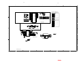
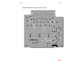
Amplifier Board Circuit Diagram:STA309A
1
1
VD3.3V
D705
LL4148
Q702
PNP_MMBT8550CLT1
VD3.3V
R739
10K
27
28
TP47
TP19
TP45
TP18
TP2
TP39
TP38
TP46
+
C716
0.1uF/25V/Y5V
CE723
47uF/50V
47K
Q701
PDWN R711
TP49
3.3V
TP40 +12V
TH_WAR
PDWN
TP50
TP48
1/2power-control
TH_WAR
RESET
R701
33
AM_SDA
AM_SCL
R703
R702
33
33
ASDAT2
ASDAT1
ASDAT0
LRCLK
BCK
D
R709
R708
R707
R706
R705
U703
25
26
C705
15pF/50V/NP0
C710
D
R704
33
10K
VD3.3V
3.3V
FB712
500/800mA
C731
VD3.3V
R777
10K
R713
10K
C712
0.1uF/25V/Y5V
MCK
R798
0.1uF/25V/Y5V
+3.3V
1
2
3
4
5
6
7
8
9
10
11
12
13
14
15
16
D
D
FB711
500/800mA
R712
10K
C713
0.1uF/25V/Y5V
33
33
33
33
33
C701
15pF/50V/NP0
C715
0.1uF/25V/Y5V
33
EAPD
MOV
GND
VDD3.3
GND
NC
SDI_78
SDI_56
SDI_34
SDI_12
LRCK1
BICK1
VDD3.3
GND
NC
RESET
PLLB
IC_84P_STA309A
VD3.3V
C717
0.1uF/25V/Y5V
CH2A
OUT2A
OUT2B
NC
GND
VDD
OUT3A
OUT3B
OUT4A
OUT4B
OUT5A
OUT5B
NC
GND
VDD3.3V
OUT6A
OUT6B
48
47
46
45
44
43
42
41
40
39
38
37
36
35
34
33
CH3A
CH4A
CH5A
C721
C720
C719
47pF/50V/NP0
C733
CH6A
D
2
C732
VD3.3V
47pF/50V/NP0
+
C718
0.1uF/25V/Y5V
CE721
22uF/16V
D
C723
47pF/50V/NP0
D
D
+ CE717
C724
22uF/16V
0.1uF/25V/Y5V
CH1A
R767
1K
TP42
TP43
0.1uF/25V/Y5V
D
TP44
GND
DC714
VD3.3V
NPN_3DG3904M
R796
47K
64
63
62
61
60
59
58
57
56
55
54
53
52
51
50
49
R710 1K
PDWN
SDIO_78
SDIO_56
NC
GND
VDD
SDO_34
SDI_12
LRCKO
BICKO
NC
GND
VDD
EPAD
OUT1A
OUT1B
AM_MUTE
R805
SA
SDA
SCL
XT1
FIL
NC
GNDA
VDDA
CKOUT
NC
GND
VDD3.3
OUT8_B
OUT8_A
OUT7_B
OUT7_A
D712
LL4148
47pF/50V/NP0
24PIN/0.5mm
TP41
47pF/50V/NP0
XP701
ASDAT0
LRCLK
ASDAT1
ASDAT2
BCK
GND
MCK
GND
AM_SCL
AM_SDA
GND
AM_MUTE
RESET
47pF/50V/NP0
2
24
23
22
21
20
19
18
17
16
15
14
13
12
11
10
9
8
7
6
5
4
3
2
1
17
18
19
20
21
22
23
24
25
26
27
28
29
30
31
32
TOP
D
R800
0/NC
0.1uF/25V/Y5V
D
D
VD3.3V
R714
3.3K
3
FB715
500/800mA
3
C727
C729
1200pF/50V/X7R
100pF/50V/NP0
C728
220pF/50V/NP0
C730
0.1uF/25V/Y5V
+ CE704
C726
0.1uF/25V/Y5V
22uF/16V
R799
0
D
4
4
A
B
C
D
E
7-3
7-3
B
C
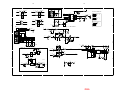
Amplifier Board Circuit Diagram:STA518
L708
D
E
10uH/5A
13
14
U701
IC_36P_STA518
36
C734
35
C735
0.1uF/50V/X7R
0.1uF/50V/X7R
34
33
D
CH6A
31
CH3A
29
CH4A
28
R716
10K
CE705
27
+ C745
100uF/16V
R717
10K
0.1uF/25V/Y5V
26
25
EAPD
24
FB713
75/200mA
IN1A
OUT2A
TH-WAR
OUT2A
FAULT
OUT1B
TRI-STATE
OUT1B
PWRDN
VCC1B
CONFIG
GND1B
VL
GND1A
VDD
VCC1A
VDD
OUT1A
GND-Reg
OUT1A
GND-CLEAN
NC
6
7
C751
C748
1uF//50V/X7R
C741
14
15
17
C753
0.47uF/63V
680pF/50V/X7R
0.1uF/50V/X7R
680pF/50V/X7R
R727
10
0.1uF/50V/X7R
18
C775
D
C768
0.47uF/63V
0.1uF/50V/X7R
CE711
220uF/35V
CE713
C778
220uF/35V
R729
4.7K
22uH/3.3A
CE715
220uF/35V
R723
4.7K
CE718
220uF/35V
D
31
30
29
28
TH_WAR
27
CE707 +
C756
100uF/16V 0.1uF/25V/Y5V
26
R736
10K
25
EAPD
24
23
75/200mA
22
CE708
100uF/16V
21
C798
+
C758
20
0.1uF/50V/Y5V
19
0.1uF/25V/Y5V
VCC-Sign
SUB-GND
VCC-Sign
OUT2B
VSS
OUT2B
VSS
VCC2B
IN2B
GND2B
IN2A
GND2A
IN1B
VCC2A
IN1A
OUT2A
TH-WAR
OUT2A
FAULT
OUT1B
TRI-STATE
OUT1B
PWRDN
VCC1B
CONFIG
GND1B
VL
GND1A
VDD
VCC1A
VDD
OUT1A
GND-Reg
OUT1A
GND-CLEAN
NC
D
CE719
220uF/35V
+35.5V
CE720
220uF/35V
CE724
220uF/35V
+
32
CH2A
CE716
220uF/35V
+
D
CH1A
33
CE714
220uF/35V
R750
4.7K
+
CH5A
34
CE712
220uF/35V
+
0.1uF/50V/X7R
R749
4.7K
0.1uF/50V/X7R
L704
+35.5V
+
C777
R406
4.7K
0.1uF/50V/X7R
R722
4.7K
C764
C749
16
1
2
L705
2
22uH/3.3A
R751
3
4
R720
10
1uF//50V/X7R
C742
C789
5
7
C744
C761
0.47uF/63V 0.1uF/50V/X7R
680pF/50V/X7R
C739
1uF//50V/X7R
6
4.7K
R754
4.7K
R725
4.7K
R752
4.7K
D
9
C779C780C782
R728 4.7K
C760
8
0.1uF/50V/X7R
R726 0.1uF/50V/X7R
0.1uF/50V/X7R
4.7K
D
0.1uF/50V/X7R
10
L706
22uH/3.3A
11
12
R731
10
13
1uF//50V/X7R
C759
1uF//50V/X7R
C746
14
15
16
C766
680pF/50V/X7R
C762
R733
10
17
18
C767
D
680pF/50V/X7R
L707
R732
4.7K
C770
0.47uF/63V
C773
0.1uF/50V/X7R
R753
4.7K
R734
4.7K
C771
0.47uF/63V
22uH/3.3A
D
C772
0.1uF/50V/X7R
0.1uF/50V/X7R
+35.5V
CE709
+
820uF/50V
C763
0.1uF/50V/X7R
D706
LL4148
D707
LL4148
D708
LL4148
CE740
4.7uF/50V
R742
1K
+
3
D
CE733
4.7uF/50V
R743
1K
+
CE734
4.7uF/50V
R744
1K
+
D709
LL4148
D710
LL4148
CE735
4.7uF/50V
+
+
3
4
-
U705A
AS4558M
2
1
R773
15K
C785
8
1/2power-control
+
R771
2.7K
CE732
4.7uF/50V
+12V
4.7uF/50V
R746
1K
D711
CE737
LL4148
4.7uF/50V
R747
1K
+
R765
5.6K
CE736
R745
1K
+
D
R761
10
R766
5.6K
R772
2K
1
JK701
CON_12P_2GNDS
+
35
C754
C755
FB714
10
1uF//50V/X7R
U702
0.1uF/50V/X7R
R735
10K
C752
R719
12
13
CE725
1000UF/25V
D
2200uF/10V/NC
22uH/3.3A
IC_36P_STA518
36
D
+3.3V
L703
11
820uF/50V
C774
0.1uF/50V/X7R
C769
0.1uF/50V/X7R
C765
0.1uF/50V/X7R
2
CE722
1000UF/25V
CE741
0.1uF/50V/X7R
10
CE710
+35.5V
2200uF/10V/NC
C737
0.1uF/50V/X7R
9
R741
4.7K
R748 CE742
4.7K
C776
D
8
D
D
R740
4.7K
12
11
10
9
8
7
6
5
4
3
2
1
+
TP20
TP21
TP22
TP23
TP24
TP25
20
0.1uF/50V/Y5V
19
0.1uF/25V/Y5V
VCC2A
C757
+
6
5
4
3
2
1
C747
+
GND2A
IN1B
C743
0.47uF/63V 0.1uF/50V/X7R
680pF/50V/X7R
C738
C750
0.1uF/50V/X7R
6
5
4
3
2
1
100uF/16V
GND2B
IN2A
1uF//50V/X7R
C736
+
CE706
XS703
6PIN/2.5mm
21
IN2B
R718
10
1uF//50V/X7R
C740
4
5
12
11
10
9
8
7
6
5
4
3
2
1
+
22
C797
VCC2B
22uH/3.3A/NC
+
23
+3.3V
OUT2B
VSS
3
SUBSUB+
SLSL+
SRSR+
CENCEN+
FLFL+
FRFR+
+
TH_WAR
VSS
L702
2
+
30
OUT2B
+
1
SUB-GND
VCC-Sign
TP26
TP27
TP28
TP29
TP30
TP31
TP32
TP33
TP34
TP35
TP36
TP37
+
32
VCC-Sign
1
GND
GND
A
0.1uF/25V/Y5V
R769
15K/1%
R770
150K
R768
68K
3
SUB+
SL+
SR+
FR+
FL+
CEN+
+ CE730
100uF/16V
R806 R807
2.2K 2.2K
R808 R809
2.2K 2.2K
R810 R811
2.2K 2.2K
D
C783
0.1uF/25V/Y5V
C781
0.1uF/25V/Y5V
D
D
D
D
U705B
AS4558M
6
+
5
4
-
4
4
8
7
A
B
C
D
E
7-4
7-4
C
D
R540B
470pF/250VAC
R540C
T531
PQ3230
1
VDD
8T531P
9
3
A8
A9
C531
4700pF/400VAC
2
100uF/400V
100uF/400V
D
10
12
A10
A12
C539
R537
2M/5%
D531A
FR207/2A/1000V
R532
NC
D532
D
V
U531
TOP258EN
CONTROL
C536
FR104/1A/400V
T531F 6
R547
R571
10 mR
R572
10K/1%
ZD532
BZX79C12
2
R503
150
R502C
R502D
NC
NC
R505
150
CY501
470pF/250VAC
HV
1
VDD
CY502
470pF/250VAC
R524
150
2
4
3
D562
D561
HV
9T501P12
D
11
T531N
12
7T501P5
1
R505A
150K
R505B
150K
R505C
150K
R501
T531F6
D505
FR107/1A/1000V
T501F2
5
T501G1
2
VDR/560V
6
8T501N
7
F501
8
Alternative
Q563
NPN_3DG3904M
1K
2
Q562
NPN_MMBT8050CLT1
C561
0.1uF/50V/X7R
R563
1K
S
Drain
NC
S
BP/M
S
S
1
3
R507
150
EN/UV
1
R508
1M
Q501
PNP_MMBT8550CLT1
1N4148
Q502
PNP_MMBT8550CLT1
1
2
1M
2PIN/7.92mm
C502
0.47uF/63V
6
ZD502
BZX79C18
D506
+10V
FR107/1A/1000V
D512
CE506
1000uF/16V
CE507
470uF/16V
R521
NC
Alternative
R523
CE505
10uF/16V
T501P5
D514
MBRF1045/10A/45V
FR107/1A/1000V
+
R517
NC
+12V
FR107/1A/1000V
8
D509
SR360/3A/60V
D510
SR360/3A/60V
Alternative
T501N
CE508
47uF/50V
R515
NC
R568
C563
1K
0.1uF/50V/X7R
R564
1K
C562
0.1uF/50V/X7R
R518
2.49K/1%
+
CE509
2200uF/16V
+
CE510
1000uF/16V
C505
R516 10K
+
CE511
1000uF/16V
Alternative Alternative Alternative
R511 470
R512
2.2K
1
4
2
3
U502
BPC-817B
PCON
1
2
3
4
5
6
7
8
3
CN502
8PIN/2.5mm/80mm
1
1:-24V
2 1
2:GND
3 2
3:+12V
4 3
4:GND
5 4
5:M+5V
6 5
6:M+5V
7 6
7:P_on/off
8 7
8
8:GND
Alternative
3.3uH
2.2M
M+5V
8PIN/2.5mm
R513
22
L502
CE504
47uF/35V
100
ZD503
BZX79C11
1
2
3
4
5
6
7
8
D508
C504
2200pF/50V/X7R
T501F2
R522
100K
R526
+
8T501N
T501G4
R504
+
Alternative
10 T501P24
+
R509
9
T501D3
2
22K
D507
XP501
T501P12 SR3100/3A/100V
D513
5
4
1
T3.15AH/250VAC
1
2
PNP_3CG3906M
Q564
OPP
L503
3.3uH
7
U501
TNY179PN
CY505
470pF/250VAC
CN501
R569
1K
R579
R514
22
Alternative
P
T501
EF25
Alternative
FB
1M
TR501
NTC/3ohm/5A
Q561
NPN_MMBT8050CLT1
HER203G/2A/200V
470pF/250VAC
RV501
3
R570
100
D511
CY504
10
T501P24
P-GND
C503
1000pF/1KV
R505D
150K
8T501N
6T501P5
NC
ZD561
BZX79C33
Alternative Alternative
470pF/250VAC
3
T501D
NC
R562
2.2K
MBRX120/20V/1A
R566
2.2K
U561
BPC-817B
R561
1.5K
Remote on/off
Standby mode: Q561, D561 OFF; D562 ON
On mode: Q561, D561 ON; D562 OFF
CY503
C501
2200pF/1KV
5
HV
A11
A12
T531G5
+33V
N.C
6.6mH
CX501
0.33uF/250VAC
R502A
R502B
1.5K
R546
NC
1N4148
22
T5011
EEL19
T531D3
R545
2.67K/1%
2
ZD531
BZX79C8V2
R567
0.1uF/50V/X7R
1
T531P
LIF501
RV504
200V/500A
110K/1%
OP
R560
8
9
C573
0.1uF/50V/X7R
R565
1K
C534
R533
NC
A8
A9
1
OPP Circuit
R574
CE537
22uF/50V
C535 0.1uF/50V/X7R
R543
10K
U533
AZ431LBZ
T5311
ER28
CX502
0.33uF/250VAC
OP
2.2K
U532
BPC-817B
3
C532
0.1uF/50V/X7R
Alternative
CE532
10uF/50V
R577
22K/1%
P
100
+
D535
1N4148
R573
1K
LIF502
6.6mH
C571
0.1uF/50V/X7R
FB
R539
CE531
+
47uF/35V
OPP
D572
1N4148
1
R542
S X F
R525
150
+
2 -
R550
33.2K/1%
0
P
P-GND
R540
0
R538
6.8
D536
1N4148
+
C
100pF/1KV
FB1
FB90@100MHz
0
R548
T531N
T531G 5
CE535
820uF/50V
CE533
820uF/50V
M+5V
R576
1K
P
U571A
LM358/SO
M+5V
0.01uF/400V
R541
1K
+
3
+
1
100uF/400V
C540
220pF/1KV
C572
0.1uF/50V/X7R
2
CE503
+
R544
33.2K/1%
1:+33V
2:+33V
3:+33V
4:GND
5:GND
6:GND
+10V
CE502
+
3
0
Q571
PNP_MMBT8550CLT1
R578
10K
CN531
6PIN/2.5mm/70mm
1
2 1
3 2
4 3
5 4
6 5
6
C538
0.1uF/50V/X7R
R575
10
1
2
3
4
4
3
CE501
+
4 -
2
T531D
+33V
2.9uH
N.C
R531
NC
Alternative Alternative
L531
10A/200V
1
Alternative
22
R549
2
+ 1
BD501
KBP306
1
2
3
4
+
1
XP502 4PIN/2.5mm
1500pF/1KV
2
D533
47K/2W
R534
R536
2M/5%
C533
1
Alternative
HV
22
4
CY506
Power Board Circuit Diagram:
E
22
8
R540A
PCON
B
3
A
DVD mode
T501:EEL19
U501:TNY177P
+12V:
D511:FR107
C503:NC
R514:NC
CE506:470uF/25V
CE507:220uF/25V
+5V:
D510:NC
CE509:1000uF/16V
CE510:NC
CE511:470uF/16V
3
0.1uF/50V/X7R
U503
AZ431LBZ
BD mode
T501:EF25
U501:TNY179P
+12V:
D511:HER203
C503:1000pF/1kV
R514:22/1206
CE506:1000uF/16V
CE507:470uF/16V
+5V:
D510:SR360
CE509:2200uF/16V
CE510:1000uF/16V
CE511:1000uF/16V
1
4
2
4
R520
NC
R519
2.4K/1%
* CAUTION :
THE PARTS MARKED WITH
ARE IMPORTANT PARTS ON THE SAFETY.
PLEASE USE THE PARTS HAVING THE DESIGNATED PARTS NUMBER WITHOUT FAIL.
A
B
C
D
E
7-5
7-5
A
B
C
D
E
Main Board Circuit Diagram: Power Supply
+12V: +12V(+-10%)
+5V: +5V(+-2.5%)
1
OFF-PAGE CONNECTION
TO POWER BOARD
8
7
6
5
4
3
2
1
8
7
6
5
4
3
2
1
MO_VCC
POWER_ON/OFF
POWER_ON/OFF
VCC
C125
0.1uF/25V/Y5V
FB1
300/2A
R1
R14
XP1
8PIN/2.5mm
0/NC
Q1
PNP_PBSS5320T
1
[2]
C2
0.1uF/25V/Y5V
C3
1uF/50V/Y5V
4.7K
+12V: +12V(+-10%)
+5V: +5V(+-2.5%)
URST#
AVCC
FB2
500/500mA
+
CE1
47uF/16V
MO_VCC
C1
0.1uF/25V/Y5V
ᬍЎ0603
URST#
AVCC
R3
0/NC
+12V
Q2
PNP_MMBT8550CLT1
+P12V
C4
0.1uF/25V/Y5V
R4
R2
200
+12V
R6
EN1
C5
100mA
+
4.7K
22K
EN1
DV33
CE2 0.1uF/25V/Y5V
47uF/16V
RFV33
R7
RFV33
0
+
R5
1.3K
EN1
LL4148
EN
D72
C6
0.1uF/25V/Y5V
CE3
47uF/16V
2
PCON
PCON
1K
FB3
500/500mA
+
CE4
47uF/16V
4.7K
R74
R12
DV33
C7
0.1uF/25V/Y5V
0/NC
3V3
P_ASM3403
1.3K
S
G
C8
1uF/50V/Y5V
R8
R11
2
89G_3V3
Q3
NPN_3DG3904M
EN
R10
R9
PNP_MMBT2907ALT1
Q32
27K
+P12V
D
Change
Q6
to
R15
RESET Circuit
R18
15K/1%
R19
3.3K
R20
22K
TP1
URST#
EN1
-24V
FB4
500/500mA
C9
0.1uF/25V/Y5V
For StandBy power
220
4.7K
Q5
NPN_3DG9014M
R434
0/NC
ASM3403;
89G_3V3
R13
-P24V
PMOS
0/NC
R21
3.3K
Q8
NPN_3DG3904M
R89
Cx
R22
3
4.7K/1%
+
CE5
22uF/10V
VCC
D1
370mA
RL207/2A/1000V
440mA
R16
0
AM_RST
Q9
NPN_3DG3904M
C10
0.1uF/25V/Y5V
Cx Close to IC pin
3
4.3/2W
R17
1/1W
REGO2
20K/1%
+
REGO1
R26
C761
CE7
220uF/16V
1000pF/50V/X7R
C12
0.1uF/25V/Y5V
R25
2
3
Vin Vout
5
Vss
CE
NC
CE6200
4
C102
C11
0.1uF/25V/Y5V
C101
0 NC
C762
CE6
220uF/16V 1000pF/50V/X7R
3V3
U20
1
+
51K/1%
R650
0.1uF/25V/Y5V
R24
R23
MO_VCC
0.1uF/25V/Y5V
DV33
V12
Q7
PNP_3CA8550D
TR_B2
Q10
PNP_3CA8550D
TR_B1
10K/1%/NC
12K/1%
4
4
A
B
C
D
E
7-6
7-6
A
B
C
D
E
OFF-PAGE CONNECTION
Main Board Circuit Diagram:MT1389GH
SP-A
DQ[0..15]
OP-
10K
1
1
C13
0.1uF/25V/Y5V
R30
3V3
3
V12
C14
D2 2
0.1uF/25V/Y5V
BAT54C
OPO
10K
C15
4.7uF/10V/Y5V
C16
0.1uF/25V/Y5V
RFV12-1
FB5
500/500mA
C33
4.7uF/10V/Y5V
R32
SP-A
SP+
LIMIT
10K
SLSL+
1
2
3
4
5
6
1
2
3
4
5
6
560/1%
0
VR_CD
R37
0
VR_DVD
TROUT R39
0
GPI36
R40
0
GPIO35
R41
0
GPIO34
XI
XO
V20
V1P4
GPO5
MDI1
LDO1
89G_3V3
LDO2
FB13
AVDD33
DMO
500/500mA
C32
C34
FMO
4.7uF/10V/Y5V0.1uF/25V/Y5V PIN_15
PIN_16
TRO
FOO
GPIO2
USB_DP
89G_3V3
C36
C76
USB_DM
0.1uF/25V/Y5V
10uF/10V/Y5V
USB_V33
Close to IC Pin
FB17
GPIO37
500/500mA
R52
5.1K/1%
USB_V12
FB18
A_SW1
V12
A_SW0
500/500mA
C38
MIC_CON
C113
TP14
DV_Y2
10uF/10V/Y5V
0.1uF/25V/Y5V
DV_Y3
DV_Y4
VSTB
DV_Y5
VSCK
DV_Y6
VSDA
DV_Y7
SF_CS
SF_DO
SF_DI
C157
1000pF/50V/X7R
MDI1
LD-CD
TP3
E
AVCC1
V20
F
B
A
RFO
IOA
D
C
TT+
F+
F-
C39
0.1uF/25V/Y5V L1
10uH/0.28A/NC
R53
C158
1000pF/50V/X7R
89G_3V3
0
RxD
TxD
C40
Q14
120pF/50V/NP0
PNP_3CG9012M
L2
R54
10uH/0.28A/NC
LDO2
0
XP3
24PIN/0.5mm
R56
4.7
R57
4.7
CE21
47uF/16V
+
Q17
PNP_3CG9012M
CE22
47uF/16V
SF_CK
UP1_6
UP1_7
URST#
RFV33
Q15
R55
10K
PNP_3CG9012M
GPIO32
FS
GPO14
DACVDD3
DACVDD3
CVBS_OUT
V_G
DACVDD3
V_R
V_B
V1.0
D3
RFV33
LL4148
R58
33K
TP13
Q16
R59
10K
PNP_3CG9012M
+
LDO1
CE23
100uF/25V
FOSO
TRSO
FMSO
DMSO
R60
R61
R62
R63
27K
27K
15K
10K
0
FOO
TRO
FMO
DMO
89G_3V3
MO_VCC
MO_VCC
4
BCK1
R655
33
MCK1
R656
33
C128
LRCK
R66
R67
R68
4.7K
4.7K
4.7K
RS-232
C123
100pF/50V/NP0
FB29
500/500mA
27pF/50V/NP0
MCK
C126
VIDEO I/F
ASDAT1
ASDAT2
ASDAT0
GPIO20
HSYNC
GPIO21
VSYNC
GPIO32
LRCK
BCK
MCK
SCART1
AUDIO_MUTE
SCART2
GPIO34
SCART_CON
TX1+
TX1-
FB12
500/500mA
C31
0.1uF/50V/Y5V
R47
6.8K
[3]
SF_CK
SF_CS
SF_DI
SF_DO
[3]
[3]
[3]
[3]
CVBS_OUT
V_R
V_B
V_G
[6]
[6]
[6]
[6]
SCART1
SCART2
SCART_CON
[6]
[6]
ASDAT1
ASDAT2
ASDAT0
[4]
[4]
[4]
LRCK
BCK
MCK
[4]
[4]
[4]
[4]
[5]
SPDIF_IN1
SPDIF_IN2
SPDIF_IN1
SPDIF_IN2
[5]
[5]
DSP_SCL
DSP_SDA
DSP_RST
[4]
[4]
[4]
ADC_VRST#
[5]
POWER
[5]
ADC_VRST#
Close to PIN
R51
Q39
D
FB16
500/500mA
N_ASM3402M
2.49K/1%
C37
CE19
0.1uF/25V/Y5V4.7uF/10V/Y5V
HPLG
3V3
S
R370
V12
MA3
MA2
MA1
MA0
MA10
BA1
BA0
FB14
RAS#
CAS#
500/500mA
1K
+12V
3V3
89G_3V3
R152 R134
10K
10K
R101
10K
89G_3V3
MA4
MA5
MA6
PDN
AMP_DET
PDN
AMP_DET
SHUTDOWN
BKEN_ERR
SHUTDOWN
BKEN_ERR
A_SW0
A_SW1
R131 R155
10K
10K
WE#
A_SW0
A_SW1
AMP_DET
ACK
PDN
RC6
GPIO19 R180
0 ADC_DAT
DV_Y2
0
R192
AM_SDA
DSP_SDA
AM_SCL
GPO14
AUDIO_MUTE
DV_Y3
SPDIF_IN1
DV_Y4
SPDIF_IN2
GPIO31
ADC_VRST#
VSTB
VSCK
VSDA
IR
PW_KEY
VSTB
VSCK
VSDA
IR
PW_KEY
MIC_DET
MIC_DET
MIC_CON
STBY
TROPEN
TRCLOSE
TRIN
TROUT
TT+
FF+
SLSL+
SPSP+
FOSO
TRSO
FMSO
DMSO
V1P4
RDS_DATA
TU_RST
TU_SCL
TU_SDA
MA7
MA8
MA9
USB Connector
[3]
[3]
[3]
[3]
[3]
[3]
[3]
[3]
[3]
[3]
[3]
[3]
[3]
[3]
[3]
[3]
[3]
[3]
TXC+
TXCTX0+
TX0TX1+
TX1TX2+
TX2-
[6]
[6]
[6]
[6]
[6]
[6]
[6]
[6]
HPLG
[6]
3
TXC+
TXCTX0+
TX0TX1+
TX1TX2+
TX2-
DSP_SCL
USB signal:
1),Via on signal is forbidden;
2),Differential impedance must control at 90 ohm.
MIC_CON
STBY
TROPEN
TRCLOSE
TRIN
TROUT
TT+
FF+
SLSL+
SPSP+
FOSO
TRSO
FMSO
DMSO
V1P4
SERVO I/F
HPLG
UP1_[6..7]
UP1_[6..7]
4PIN/2.0mm
XP4
4
3 4
2 3
1 2
1
USB_DP
USB_DM
VCC_USB
PNP_PBSS5320T
R65
1
2
3
4
220
C51
6pF/NC
EN1
[6]
TMDS I/F
FAN1
Q18
2
AUDIO I/F
FAN1
HDMI_CEC
HDMI_CEC
TU_SCL
TU_SDA
TU_RST
TU_SCL
TU_SDA
TU_RST
RDS_DATA
C52
6pF/NC
URST#
RDS_DATA
URST#
AM_SDA
AM_SCL
[1]
AM_SDA
AM_SCL
VSDA
4
C53
C54
C55
C56
0.1uF/25V/Y5V0.1uF/25V/Y5V0.1uF/25V/Y5V0.1uF/25V/Y5V
A
DCKE
MPEG_MUTE
PTC/1.5A/6V
1
2
3
4
[3]
[3]
[3]
[3]
ADC_DAT
POWER
TXC+
TXC-
USB I/F
[3]
DCLK
RAS#
CAS#
WE#
ADC_DAT
DSP_SCL
DSP_SDA
DSP_RST
TX0+
TX0-
XP5
4PIN/2.0mm
VSTB
SCART1
SCART2
SCART_CON
C29
6800pF/50V/X7R
89G_3V3
DV33
RxD
TxD
AADVDD
FB10
500/200mA
BCK
C127
V12
AM_SCL
[3]
BA[0..1]
1
CVBS_OUT
V_R
V_B
V_G
89G_3V3
TX2+
TX2-
AM_SDA
VCC
MO_VCC
VSCK
V12
33
U1
MT1389GH/176
TR1
C45
C46
C47
C48
C49
C50
0.1uF/25V/Y5V0.1uF/25V/Y5V0.1uF/25V/Y5V0.1uF/25V/Y5V0.1uF/25V/Y5V0.1uF/25V/Y5V
R654
[3]
DQM[0..1]
S-FLASH
ASDAT0
LRCK1
DCKE
SF_CK
SF_CS
SF_DI
SF_DO
V12
TP12
C41
C42
C43
C44
330pF/50V/X7R
330pF/50V/X7R
0.1uF/25V/Y5V
0.015uF/50V/Y5V
V1P4
Chip De cap.
BKEN_ERR
[3]
MA[0..11]
DRAM I/F
Audio
0
R75 R102
C23
27pF/50V/NP0
ASDAT2
R653 33
TP10
GPIO31
TP11
GPIO30 SHUTDOWN
GPIO29
BKEN_ERR
132
131
130
129
128
127
126
125
124
123
122
121
120
119
118
117
116
115
114
113
112
111
110
109
108
107
106
105
104
103
102
101
100
99
98
97
96
95
94
93
92
91
90
89
DQ13
DQ12
DQ11
DQ10
DQ9
DQ8
DQM1
DCLK
MA11
LD-DVD TP2
LQFP176
DQ0
DQ1
DQ2
DQ3
DQ4
DQ5
DQ6
DQ7
DQM0
DQ15
DQ14
Very Important to
reduce Noise
R64
DSP_SCL
DSP_SDA
DSP_RST
POWER
AMP_DET
PDN
GPIO8
HDMI_CEC
R50
45
46
47
48
49
50
51
52
53
54
55
56
57
58
59
60
61
62
63
64
65
66
67
68
69
70
71
72
73
74
75
76
77
78
79
80
81
82
83
84
85
86
87
88
R49
0
XO
Put these circuits as
closer as possible to
MT1389
ASDAT1
R652 33
DCLK
RAS#
CAS#
WE#
27pF/50V/NP0
GPIO31
GPIO30
GPIO29
GND33
AGND12
TX2P
TX2N
AVDD12_D
TX1P
TX1N
AGND12
TX0P
TX0N
AVDD12_C
TXCP
TXCN
AGND12_TX2
AGND33_TX
AVDD33_12
EXT_RES
AVSS12
GPIO10 / HPLG
SPDIF / GPIO12
DVDD12
RA3
RA2
RA1
RA0
RA10
BA1
BA0
DVDD33
RAS_
CAS_
GND12
RWE_
GND33
RA4
RA5
RA6
DVDD33
RA7
RA8
RA9
MT1389GH
IR
0
MIC_DET
0
FB15
C35 +
500/500mA
0.1uF/25V/Y5V
CE17
100uF/25V/NC
PCON
MO_VCC
VR_CD
VR_DVD
Option1
AVDD12_2
AVDD33_1
XTALI
XTALO
AGND33
V20
V14
REXT / GPO5
MDI1
LDO1
LDO2
AVDD33_2
DMO
FMO
TRAY_OPEN
TRAY_CLOSE
TRO
FOO
FG / GPIO2
USB_DP
USB_DM
VDD33_USB
VSS33_USB
PAD_VRT / GPIO37
VDD12_USB
YCLK
DV_Y0
DV_Y1
DV_Y2
DV_Y3
DV_Y4
DV_Y5
DV_Y6
DV_Y7
SF_CS_
SF_DO
SF_DI
DVDD33
SF_CK
UP1_6 / SCL
UP1_7 / SDA
GPIO11
GPIO6
PRST_
POWER_ON/OFF
IOA
1
2
3
4
5
6
7
8
9
10
11
12
13
14
15
16
17
18
19
20
21
22
23
24
25
26
27
28
29
30
31
32
33
34
35
36
37
38
39
40
41
42
43
44
TU_RST
TU_SCL
TU_SDA
RDS_DATA
TROPEN
Option2: like 89G SERVO PIN.
RFV12-2
RFVDD3
R45
51
R46
51
PW_KEY
STBY
33
27pF/50V/NP0
RFF
RFE
RFD
RFC
RFB
RFA
RFH / OPINN
RFG / OPINP
RFIN / OPOUT / GPI36
RFIP
AGND12
AVDD12
ADACVDD2
ADACVDD1
CENTER / GPIO
ALS / GPIO
AL / GPIO1
AVCM
AR / GPIO0
ARS / GPIO
LFE / GPIO
ADACVSS1
ADACVSS2
PAD_APLLCAP / GPIO35
APLLVDD_GPIO / GPIO34
AADVDD
AKIN1 / GPIO21
ADVCM / GPIO20
AKIN2 / GPIO19
AADVSS
R
B
AGNDC
G
DACVDDA
AGNDC
DACVDDB
CVBS
DACVSSC
FS
VREF / GPO14
DACVDDC
DVDD33
GPIO32
LIMIT
26
25
GND
GND
R35
C30
1uF/50V/Y5V
GPIO35
GPIO34
AADVDD
GPIO21
GPIO20
GPIO19
TRCLOSE
ASDAT2-1
BCK1
MCK1
GPO5
RFV12-1
TRIN
PIN_16
R651
ASDAT0-1
89G_3V3
CE14
10uF/25V
Y1
XI
176
175
174
173
172
171
170
169
168
167
166
165
164
163
162
161
160
159
158
157
156
155
154
153
152
151
150
149
148
147
146
145
144
143
142
141
140
139
138
137
136
135
134
133
GPIO2
+
ADACVDD
ASDAT0-1
LRCK1
ASDAT1-1
E
F
D
A
B
C
OPOPO
GPI36
RFO
+
C28
CE13
0.1uF/25V/Y5V
47uF/16V
+
3
R33
BA[0..1]
100K
27MHz/30PPM
C22
27pF/50V/NP0
ASDAT2-1
C26
4.7uF/10V/Y5V
IR
GPIO3 / INT_
GPIO4
DV_C0
DV_C1
DV_C2
DV_C3
DV_C4
DV_C5
DV_C6
DV_C7
SD_MS_CLK
DVDD33
SD_MS_CMD
SD_MS_D0
SD_MS_D1
SD_MS_D2
SD_MS_D3
GPIO13
GPIO9
GPIO8
GPIO7 / CKE_
DVDD33
RD0
RD1
RD2
RD3
RD4
RD5
RD6
RD7
DQM0
RD15
RD14
DVDD12
RD13
RD12
RD11
RD10
RD9
RD8
DQM1
RCLK
RA11
FF+
T+
TC/c
D/d
CD/DVD SW
RF
A/a
B/b
F
GND-PD
Vc(Vref)
Vcc
E
NC
VR-CD
VR-DVD
CD-LD
MD
HFM
NC
DVD-LD
GND-LD
1
2
3
4
5
6
7
8
9
10
11
12
13
14
15
16
17
18
19
20
21
22
23
24
0.1uF/25V/Y5V0.1uF/25V/Y5V
CE9
10uF/25V
C25 100uF/25V
0.1uF/25V/Y5V
CE11
SERVO RF DeCAP.
PIN_15
1
2
3
4
5
6
7
8
9
10
11
12
13
14
15
16
17
18
19
20
21
22
23
24
+
ASDAT1-1
Close to IC Pin
RF Reference
2
0.1uF/25V/Y5V
C21
V1P4
+
C27
CE12
0.1uF/25V/Y5V
47uF/16V
1
2
3
4
5
6
7
8
9
10
11
12
13
14
15
16
17
18
19
20
21
22
23
24
C20
R29
C24
0.1uF/25V/Y5V
12 RFV12-2
XP2
6PIN/2.0mm
V20
C19
ADACVDD
FB8
500/200mA
FB7
500/500mA
+
1
3V3
R31
DACVDD3
DQM[0..1]
Crystal
89G_3V3
RFVDD3
FB6
500/500mA
C17
C18
4.7uF/10V/Y5V
0.1uF/25V/Y5V
DQ[0..15]
MA[0..11]
89G_3V3
G
R27
R28
DSP_RST
SP-
B
C
D
E
7-7
7-7
A
B
C
D
E
Main Board Circuit Diagram:SDRAM & FLASH
1
SR_3V3
R69
10K
SDCKE
DCKE R76
10K
SDCKE
R70
10K
DCS#
C58
SDCLK
15pF/NC
DCLK
BA0
BA1
R71
33
RAS#
CAS#
WE#
SDCLK
DBA0
DBA1
MA0
MA1
MA2
MA3
MA4
MA5
MA6
MA7
MA8
MA9
MA10
MA11
DBA0
DBA1
23
24
25
26
29
30
31
32
33
34
22
35
20
21
SDCLK
SDCKE
38
37
DCS#
DRAS#
DCAS#
DWE#
19
18
17
16
DQM0
DQM1
A0
A1
A2
A3
A4
A5
A6
A7
A8
A9
A10/AP
A11
BA0/A13
BA1/A12
CLK
CKE
CS
RAS
CAS
WE
15
39
54
41
28
SR_3V3
DQ[0..15]
DQM[0..1]
BA[0..1]
DCLK
RAS#
CAS#
WE#
DCKE
C59
C60
C61
C62
C63
C64
C65
0.1uF/25V/Y5V
0.1uF/25V/Y5V
0.1uF/25V/Y5V
0.1uF/50V/Y5V
0.1uF/50V/Y5V
0.1uF/50V/Y5V
0.1uF/50V/Y5V
VCC DeCap
SR_3V3
DV33
10K
1
2
3
4
U3
CE# VDD
SO HOLD#
WP# SCK
VSS
SI
8
7
6
5
HOLD#
SF_DI
R79
10K
R96
[2]
DQM[0..1]
[2]
BA[0..1]
[2]
DCLK
RAS#
CAS#
WE#
[2]
[2]
[2]
[2]
DCKE
[2]
SF_CK
SF_CS
SF_DI
SF_DO
[2]
[2]
[2]
[2]
STBY
TROPEN
TRCLOSE
TRIN
TROUT
[2]
[2]
[2]
[2]
[2]
TT+
FF+
SLSL+
SPSP+
[2]
[2]
[2]
[2]
[2]
[2]
[2]
[2]
FOSO
TRSO
FMSO
DMSO
[2]
[2]
[2]
[2]
V1P4
[2]
S-FLASH
STBY
TROPEN
TRCLOSE
TRIN
TROUT
TT+
FF+
SLSL+
SPSP+
SDR_DRAM
FOSO
TRSO
FMSO
DMSO
R77
1K
10K
SF_CK
DV33
V1P4
2
SERVO I/F
C66
0.1uF/25V/Y5V
SPI_16Mb_EN25T160
[2]
MA[0..11]
DRAM I/F
SF_CK
SF_CS
SF_DI
SF_DO
VCCQ DeCap
DV33
SF_CS
SF_DO
R78
DQ[0..15]
MA[0..11]
C57
0.1uF/25V/Y5V
SR_3V3
SDRAM_64Mb_M12L64164A-7T
2
500/500mA
6
12
46
52
VSSQ
VSSQ
VSSQ
VSSQ
VSS
VSS
VSS
FB19
FB20
500/500mA
+
CE24
100uF/25V
SR_3V3
3
9
43
49
VCCQ
VCCQ
VCCQ
VCCQ
NC
NC
DQ0
DQ1
DQ2
DQ3
DQ4
DQ5
DQ6
DQ7
DQ8
DQ9
DQ10
DQ11
DQ12
DQ13
DQ14
DQ15
1
14
27
VCC
VCC
VCC
DQML
DQMH
36
40
DRAS#
DCAS#
DWE#
2
4
5
7
8
10
11
13
42
44
45
47
48
50
51
53
DQ0
DQ1
DQ2
DQ3
DQ4
DQ5
DQ6
DQ7
DQ8
DQ9
DQ10
DQ11
DQ12
DQ13
DQ14
DQ15
DV33
1
OFF-PAGE CONNECTION
3V3
U2
SF_CS
SerialFlash
TP4
MD_VCC
TP6
R167
R159
3
1K
3K
15
16
17
18
19
20
21
TT+
SL+
SL-
C67
0.1uF/25V/Y5V
FMSO
AM_RST
TR_B2
TRSO
V1P4
STBY
R83
10K
30
22
23
24
25
26
27
28
U4
VOTK+
VOTKVOLD+
VOLDVCC2
VCCD
VCTL
G2
GND
VINLD
RESET
TRB2
VINTK
BIAS
MUTE
14
13
12
11
10
9
8
VOFC+
VOFCVOSLVOSL+
VOTR+
VOTRVCC
TP5
F+
FSPSP+
LOAD+
LOAD-
29
G1
7
6
5
4
3
2
1
REV
FWD
REGO1
VINSL+
REGO2
TRB1
VINFC
TROPEN
TRCLOSE
R80
FOSO
TP7
MD_VCC
TP8
TP9
10K
+
C68 CE26
100uF/25V
0.1uF/25V/Y5V
REGO1
DMSO
REGO2
TR_B1
VCC
FB21
500/500mA
+
CE27
47uF/16V
DRIVER_MOTO_AM5888
C70
0.1uF/25V/Y5V
TRIN
DV33
C69
0.1uF/25V/Y5V
R81
10K
TROUT
R84
10K
TRIN
AM_RST
R85
1K
C71
C72
0.1uF/25V/Y5V
0.1uF/25V/Y5V
MotorDriver
REGO1
TR_B2
REGO2
TR_B1
LOADLOAD+
R82
1K
1
2
3
4
5
TRIN
3
1
2
3
4
5
XP6
5PIN/2.0mm
REGO1
TR_B2
REGO2
TR_B1
AM_RST
4
4
MotorDriver
A
B
C
D
E
7-8
7-8
5
4
3
Main Board Circuit Diagram:AUDIO IN
AL_CH3 R164
TUNER_L
R92
1uF/50V/Y5V
AL_CH2
C163
10K
AUX2_L
R87
1uF/50V/Y5V
AL_CH3
C166
10K
R154
3K/NC
AR_CH3
R118
3K
1uF/50V/Y5V
AR_CH2
C164
10K
AUX2_R R91
1uF/50V/Y5V
AR_CH3
C167
10K
150K
AL_CH4 R173
150K
AR_CH4 R174
150K
AL_CH2
R153
3K
R157
3K/NC
D
AR_CH2
R175
150K/NC
R176
R88
R162
22K
AR_CH2
AR_CH3
AR_CH4
R163
22K
CE31
12
14
15
11
47uF/16V
150K/NC
1
5
2
4
AL_CH2
AL_CH3
AL_CH4
10
9
A_SW0
A_SW1
R103
1uF/50V/Y5V
AL_CH4
C169
100
R100
MIC_ALR
1uF/50V/Y5V
C176
R197
MIC_L
4.7K
MP3_AR
R105
1uF/50V/Y5V
AR_CH4
C170
100
G
MIC_CON
MIC_CONR114
1
2
3
4
5
MP3_AL
+12V
MP3_AR
MIC_LR
R113
R609
12VA
330
R646
R115
100/NC
R98
8
[4]
[4]
[4]
[2]
ADC_VRST#
ADC_VRST#
[2]
TUNER_L
TUNER_R
TUNER_L
TUNER_R
[8]
[8]
D
C74
470pF/50V/X7R
C75
470pF/50V/X7R
100K
MCK
LRCK
BCK
ADC_DAT
ADC & SW I/F
A_SW0
A_SW1
A_SW0
A_SW1
SPDIF_IN2
SPDIF_IN1
[2]
SPDIF_IN2
[2]
SPDIF Dx I/F
to NMOS ASM3402
REFM
22K
5
4
C611
R610
22K
47pF/50V/NP0
CE609 +
47uF/16V
R643
1
RCA/4h
P1
5.6K
C607
1000pF/50V/X7R
2
AS4558M
U602A
1
C623
5
6
2.2uF/16V/Y5V
+
7
-
U602B
AS4558M
4
AUX2_R
3
8
2.2uF/16V/Y5V
R612
10K/1%
2
-
R648
+
MIC_LR
3
4
C609
9
C
100K
R642
47K
3
REFM
12VA
C610
100pF/50V/NP0
R649
20K
CVBS_O
1
4
R94
R95
MCK
LRCK
BCK
ADC_DAT
SPDIF_IN1
47uF/16V
AUX2_L
CVBS_O
100K
AD_INL
470
AD_INR
C760
0.1uF/50V/Y5V
CE608 +
2
6
5
1uF/50V/Y5V
C175 MIC_L
R93
MIC_ALR
100/NC
6
8
7
3
470
8
1
2
3
4
5
GND
1uF/50V/Y5V
C174 MIC_R
Q19
N_ASM3402M
4.7K
Q21
NPN_3DG3904M
10K
EN
VEE
13
3V3
Change
5PIN/2.0mm
XP8
C
R106
R112
R160
3K
P5
4.7K
X0
VCC
X1
X2
X3
74HC4052
X
Y0
Y1
Y2
Y3
Y
A
B
OFF-PAGE CONNECTION
16
4.7K
4.7K
10K
U5
R99
R107
R158
3K
MIC_R
4.7K
MIC_LR
D
1uF/50V/Y5V
C168
R104
6
7
3V3
2K
+
C73
CE30
0.1uF/25V/Y5V
47uF/16V
S
MP3_AL
MIC_ALR
1
+6VA
150K
R165
+
TUNER_R R97
2
+6VA
COAX_IN
R645
C626
R156
100
MIC_ALR
20K
47pF/50V/NP0
C625
2.2uF/16V/Y5V
RCA/6h
C114
C115
C116
C117
C118
FB22
100pF/50V/NP0
100pF/50V/NP0
100pF/50V/NP0
100pF/50V/NP0
100pF/50V/NP0
R216
FB23
500/500mA
Optical
R227
6
5
+6VA
R109
1V
100K/NC
1
2
3
4
5
6
7
8
ADC_INL
+
C173
ADC_INL
5.6K R254
CE43
10uF/25V
AINR
AINL
CKS1
VCOM
AGND
VA
VD
DGND
CKS0
CKS2
DIF
PDN
SCLK
MCLK
LRCK
SDTO
U6
ADC_AK5358A
C78
0.1uF/25V/Y5V
10uF/10V/Y5V
7
47K
R110
10K
R111
10K
MBRX140/40V/1A
D73
1V
R225
10K
16
15
14
13
12
11
10
9
B
BCK
MCK
LRCK
ADC_DAT
3V3
R116
4.7K
U12B
8
C155
0.1uF/25V/Y5V
0/NC
ADC_INR
C142
47pF/50V/NP0
1K
4.7
8
5.6K R253
4
AD_INL
ADC_INR
10uF/10V/Y5V
R220
R226
P2
S/PDIF IN
C77
0.1uF/25V/Y5V R108
100K/NC
+6VA
0.1uF/25V/Y5V
R120
1
-
C156
0.1uF/25V/Y5V
Vout
G
VCC
5
+
2
1K
K1
4
C106
SPDIF_IN2
R119
75
C80
330pF/50V/X7R
R218
K2
1
2
3
AD_INR
CE40
100uF/25V
C172
4
C79
0.1uF/25V/Y5V
B
U12A
AS4558M
3
AVCC
+
10K
-
SP_VCC
3V3
500/200mA
+
SPDIF IN
MO_VCC
C138
47pF/50V/NP0
AS4558M
ADC_VRST#
R117
1K
Q23
NPN_3DG3904M
+12VA
3V3
Coaxial
5
R122
75
C83
330pF/50V/X7R
0
1
Vout
-Vs
R121
+Vs
SPDIF_IN1
+6VA
2
C81
0.1uF/25V/Y5V
U7
+IN
-IN
0.01uF/50V/Y5V
R123
AD8061/NC
L11
C82
3
4
75/NC
R124
75
+12VA
+12V
1.8uH/25mA
COAX_IN
C171
220pF/50V/NP0
R435
22K
R437
22K
D4
C153
R436
CE33
100
0.1uF/25V/Y5V
100uF/16V
+
PESD_PGB101
A
A
5
4
3
2
1
7-9
7-9
A
B
C
D
E
Main Board Circuit Diagram:VIDEO I/F
AVCC
R127
R125
SCART16
R/V
1.2uH/25mA
L3
C85
100pF/50V/NP0
75
3V3
Q24
NPN_3DG3904M
150
C84
R126
1K
0.1uF/25V/Y5V
B/U
SCART8
G/Y
R/V
SCART16
CVBS_O
V_R
R128
SCART_CON
2.2K
1
V_B
1
2
3
4
5
6
7
8
9
10
1
2
3
4
5
6
7
8
9
10
R129
OFF-PAGE CONNECTION
4.7K
B/U
1.2uH/25mA
L4
1.5K
R130
SCART_CON
SCART_CON
SCART16
CVBS OUT
0
R132
C86
100pF/50V/NP0
10PIN/2.0mm
XP10
75
V_G
75
1.5K
R133
1K
3V3
SCART2
SCART1
SCART8
C87
100pF/50V/NP0
4.7K
SCART_CON
0(
1
Q25
NPN_3DG3904M
2.2K
SCART1
CVBS_O
R143
91
100pF/50V/NP0
100pF/50V/NP0
0
9.5-12V(4:3)
0
TX0+
TX0TX1+
TX1-
SCART2
SCART2
SCART I/F
TXC+
TXC-
4.7K
SCART1
TX2+
TX2HPLG
TXC+
TXC-
[2]
[2]
TX0+
TX0-
[2]
[2]
TX1+
TX1-
[2]
[2]
TX2+
TX2-
[2]
[2]
HPLG
[2]
UP1_[6..7]
[2]
R142
2.4K
33
+
CE45
47uF/16V
82
C90
6V(16:9)
UP1_[6..7]
R141
10pF/50V/NP0
C89
1
AVCC
R433
0
1.2uH/25mA
0
3V3
Q26
R140
2.2K
NPN_3DG3904M
2
SCART2
SCART1
R139
L6
1
R135
R138
CVBS_OUT
[2]
[2]
[2]
[2]
VIDEO I/F
R137
C88
CVBS_OUT
V_R
V_B
V_G
RGB OUT
1
G/Y
1.2uH/25mA
L5
R136
SCART8
CVBS_OUT
V_R
V_B
V_G
+12V
Q27
NPN_3DG3904M
R144
3
G/Y
2
5
B/U
D5
1
PESD_PGB101
4
3
R/V
1
C93
4
R146
100
TMDS I/F
2
G/Y
PESD5VL4UG
U8
CVBS_O
R145
1.2K
5
B/U
CVBS_O
G/Y
B/U
R/V
2
P3
CVBS_O
D6
PESD_PGB101
PESD_PGB101
C91
RCA/3h
100pF/50V/NP0
100pF/50V/NP0
100pF/50V/NP0
R/V
D7
C92
D8
PESD_PGB101
CVBS_O
CVBS_O
C94
100pF/50V/NP0
DV33
1
4
L9
2ACM2012H-900-2P
3
TX0TXC+
1
4
ACM2012H-900-2P
2L8
3
TXC-
1
L10
4
HDMI_CEC
HDMI_ARC
HDMI_SCL
HDMI_SDA
C763
10PF
VCC
R148
1.5K
4
C764
10PF
D9
PESD_PGB101/NC
R147
D10
47pF/50V/NP0
PESD_PGB101/NC
FB24
500/200mA
C96
1.5K
HDMI_SCL
R150
HDMI_SDA
R151
33
33
HPLG
C95
VCC
R149
47K
120pF/50V/NP0
R166
0/NC
MO_VCC
D17
LL4148
MO_VCC
HDMI_CEC
HDMI_CEC
R659
10K
C177
U603
HDMI_ARC
0.1uF/25V/Y5V
R201
75
R202
75
MO_VCC
R660
10K
3
4
+IN
-IN
5
TX1TX0+
1
2
3
4
5
6
7
8
9
10
11
12
13
14
15
16
17
18
19
2
1
4
L7
2ACM2012H-900-2P
3
-Vs
2ACM2012H-900-2P
3
TX2TX1+
SPDIF_IN1
+Vs
TX2+
3
R209
27K
23
22
Differential Signal !
No through hole & length less than 5cm !
100 ohm - Impedance
20
21
3
Vout
1
R204
SGM8051
75
P4
HDMI JACK
R658
10K
HDMI_VCC
C97
+
CE46
0.1uF/25V/Y5V220uF/16V
UP1_6
UP1_7
4
ᬍЎ0603
A
SPDIF_IN1 [2]
SPDIF_IN1
0
R203
R657
10K
HDMI_CEC [2]
B
C
D
E
7-10
7-10
5
4
3
2
1
Main Board Circuit Diagram:AMP / FB / TUNER
BCK
MCK
AM_SCL
AM_SDA
ASDAT0
LRCK
ASDAT1
ASDAT2
BCK
TU1
TUNER_13P_A
/RST
/SEN
SCLK
SDIO
VCC(+5V)
GND
ROUT
LOUT
GPIO2
MCK
AM_SCL
AM_SDA
AMP_MUTE
DSP_RST
DSP_RST
3V3
POWER
XP11 TO AMP BD
24PIN/0.5mm
C99
POWER
AGND
R185
0 TU_RST
R186
R187
0 TU_SCL
0 TU_SDA
TU_SCL
TU_SDA
R188
R189
R190
0
0
0
TUNER_R
TUNER_L
RDS_DATA
C98
C112 C107 C108
13
12
11
10
+12V
1
2
3
4
5
6
7
8
9
GND
GND
GND
GND
1
2
3
4
5
6
7
8
9
10
11
12
13
14
15
16
17
18
19
20
21
22
23
24
26
25
GND
GND
D
1
2
3
4
5
6
7
8
9
10
11
12
13
14
15
16
17
18
19
20
21
22
23
24
C109 C110
C111
0.1uF/NC
0.1uF/NC 0.1uF/NC 0.1uF/NC
0.1uF/NC
0.1uF/NC
SHUTDOWN
AMP_DET
PDN
BKEN_ERR
TU_RST
FB25 500/500mA
TUNER_R
TUNER_L
RDS_DATA
3V3
I/F
D
TUNER_L
TUNER_R
TUNER_L
TUNER_R
[5]
[5]
+ CE47
0.1uF/25V/Y5V
47uF/16V
AGND
AGND
AGND
C100
0.1uF/25V/Y5V
0.1uF/25V/Y5V
FB26
500/500mA
FB27
500/500mA
R200
FB28
500/500mA
AMP_MUTE
MPEG_MUTE
0
C
1
2
3
4
5
6
7
8
9
10
11
12
13
14
XP12
14PIN/1.0mm
1
2
3
4
5
6
7
8
9
10
11
12
13
14
R171
MIC_DET
100
-24V
+12V
FB9
500/500mA
R168
R169
R170
100
100
R172
R161
C121
C105
100pF/50V/NP0
27pF/50V/NP0
100 VSTB
200
200
VSCK
VSDA
IR
AGND
MIC_DET
C
DV33
VSCK
VSDA
VSTB
IR
PW_KEY
C119 C103C120 C104
100pF/50V/NP0
100pF/50V/NP0
100pF/50V/NP0
C122
27pF/50V/NP0
AM_SCL
AM_SCL
[2]
AM_SDA
AM_SDA
[2]
B
B
A
A
5
4
3
2
1
7-11
Front Control Board Print-layout (top side):
7-11
7-12
Amplifier Board Print-layout (top side):
7-12
7-13
Amplifier Board Print-layout (bottom side):
7-13
7-14
Power Supply Print-layout (top side):
7-14
7-15
Main Board Print-layout (top side):
7-15
7-16
Main Board Print-layout (bottom side):
7-16
8-1
EXPLODED VIEW FOR HTS3531/12/51/94/98/F7/55/78/93
ASSY1
This is general mechanical exploded view .Please refer to the model set for the detailed information.
ASSY1 includes components:15,16,17,19,24
9-1
REVISION LIST
Version 1.0
* Initial release for HTS3531/12/51/94/98
Version 1.1
*Add HTS3531/F7
Version 1.2
*Add HTS3531/55/78
Version 1.3
*Add HTS3531/93