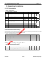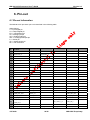
1
AML 8613 A/V Processor User’s Guide
Version 0.5
AML 8613 A/V Processor
User’s Guide
AMLOGIC, Inc.
3930 Freedom Circle
Santa Clara, CA 95054
U.S.A.
www.amlogic.com
AMLOGIC reserves the right to change any information described herein at any time without notice.
AMLOGIC assumes no responsibility or liability from use of such information.
1/07/2008
1/25
AMLOGIC Proprietary
AML 8613 A/V Processor User’s Guide
Version 0.5
Table of Contents
1.
2.
3.
Introduction ........................................................................................................................... 4
Features.................................................................................................................................. 5
Architecture Overview ........................................................................................................ 8
3.1 Architecture ................................................................................................................................8
3.2 Video/Picture Processing ...........................................................................................................8
3.3 Audio Processing .................................................................................................................... 10
3.4 Peripherals Interface Architecture........................................................................................... 10
3.5 Host CPU and System Architecture ........................................................................................ 11
4.
External Interfaces............................................................................................................. 12
4.1 Global Configurations.............................................................................................................. 12
4.2 Memory Interfaces................................................................................................................... 14
4.3 Audio Interfaces ...................................................................................................................... 16
4.4 Video Output Interfaces........................................................................................................... 17
5.
Operating Conditions ........................................................................................................ 19
5.1 DC Characteristics .................................................................................................................. 19
5.2 Absolute Maximum Ratings..................................................................................................... 19
5.3 Recommended Operating Conditions ..................................................................................... 19
6.
Pin-out ................................................................................................................................... 20
6.1 Pin-out information .................................................................................................................. 20
7.
8.
Pin-Out Diagram ................................................................................................................. 24
Mechanical Specifications............................................................................................... 25
1/07/2008
2/25
AMLOGIC Proprietary
AML 8613 A/V Processor User’s Guide
Version 0.5
Revision History
Revision
Revised Date By
Changes
Number
0.1
May 28,2008
Jesse W Initial Version
0.2
Oct 15, 2008
QL Tu
Revision
0.3
Nov 11, 2008
Julius Z
Revision
0.4
Nov 13, 2008
QL Tu
Revision
0.41
Dec 12, 2008
QL Tu
Modify reset config(remove M2), change Max SDRAM to 32MB
0.5
Jan 06, 2009
Julius Z
Revision
1/07/2008
3/25
AMLOGIC Proprietary
AML 8613 A/V Processor User’s Guide
Version 0.5
1. Introduction
The AML8613 A/V processor is a complete integrated system targeting Media box (MBX) backend applications.
The AML8613 device includes a 333 MHz embedded RISC CPU, A/V decoders, crypto-engine, transport
interface and USB for the MBX applications. The AML8613 firmware provides all A/V decoding functions, and
USB stacks.
The AML8613 combines full function of MPEG-1, MPEG-2, MPEG-4 and Real-Video decoding, numerous
dedicated and general-purpose peripherals, and a high speed 32-bit host CPU in a single device. The
AML8613 has two built-in AMRISCTM RISC processors with special instructions to accommodate audio and
video digital signal processing. The AML8613 device provides many on-chip I/O peripherals. The peripherals
include one USB 2.0 High-Speed OTG controllers and PHYs.
The embedded 32-bit core CPU controls all system related application software. It executes AVOS, the base
operating system for AML8613. All applications and drivers run on top of AVOS. Drivers including MBX
processing, USB drivers and other hardware related programming interfaces are provided by AVOS.
Applications including, graphical user interfaces, on-screen displays (OSD), and file system sub-system are
also included in AVOS. Developers can add additional applications to customize AVOS for each unique
product platform.
The core CPU interfaces to the video and audio processing hardware. MPEG1/2/4, HVD/EVD, Real-Video and
JPEG/M-JPEG streams are processed by dedicated video decoding hardware and the flexible Video
TM
engine. The hardware and microcode combination is capable of decoding normal D1 size video
AMRISC
sequence at full speed, and JPEG pictures with no limits. Pixel based de-interlacing is applied to the video
sequence for high quality video output.
Once decoded, the output pictures are passed to a sophisticated video sub-system that performs video
enhancement and scaling functions. Contrast enhancement, hue adjustment, video scaling, video interpolation,
pan-scan, letter-box, and zoom are also supported. The scalar supports both up-scaling and down-scaling of
images and video. The scalar can also mix in multiple graphics and OSD layers for the final display.
The integrated Audio AMRISCTM RISC processor performs advanced digital audio decoding and
post-processing. The micro-coded engine provides support for all existing audio formats and it also has
enough flexibility to accommodate new audio standards. Popular audio formats like MPEG, LPCM, Dolby
AC-3 5.1, HDCD, MP-3, WMA, AAC, Real-Audio can be supported. In addition, SPDIF (IEC958) outputs are
supported.
The AML8613 also integrated one USB 2.0 High Speed OTG controllers and PHYs for connecting to USB hard
disk, FLASH memory, digital cameras and MP3 players. The AVOS drivers and applications for AML8613
firmware includes the basic USB device driver, USB protocol stacks to support bulk and INTR transfer, Hub,
Mass-Storage (MS) class, Picture Transfer Protocol (PTP) and PictBridge protocol. The AVOS USB firmware
also supports multiple file systems and includes flexible file transfer functions between USB devices.
AML8613 A/V processor has a set of very flexible clocking circuits that implement the adaptive AMPOWER-II
power reduction algorithms. The chip works in conjunction with the AVOS software to reduce total power
consumption based on processing load, type of media streams being processed and the output requirements.
With AMPOWER-II, the system can reduce power consumption for portable applications and helps consumer
electronics to achieve the Energy Star rating.In addition, AMPOWER-II also provides higher performance
within smaller, thermally constrained environments.
1/07/2008
4/25
AMLOGIC Proprietary
AML 8613 A/V Processor User’s Guide
Version 0.5
2. Features
The AML8613 chip is very flexible and most of the capabilities are under firmware control. The following list of
features may or may not be included in the firmware library or binary, depending on the actual application and
platform.
High Integration
•
•
•
•
•
Embedded 32-bit core RISC processor for system control
Complete RealVideo, MPEG 1/2/4 decoding backend and video post processing logic
Complete audio decoding backend
Integrated one USB 2.0 High Speed OTG ports
Integrated TV encoder and triple video DACs
RealVideo Decoding
•
•
•
RealVideo decoding engine controlled by a dedicated Video AMRISCTM processor
Decodes RealVideo-8/9/10 video streams
*.rm and *.rmvb file formats can be handled by AVOS
MPEG 1/2 Decoding
•
•
•
•
•
•
MPEG video engine controlled by a dedicated Video AMRISCTM processor
MPEG-2 ML/MP conforming to ISO-13818
MPEG-1 ML/MP conforming to ISO-11172
Sub-picture and highlight decoding and display
Advanced error detection, concealment, and recovery scheme
*.mpg, *.mpeg, *.dat, and *.avi file formats can be handled by AVOS and CPU subsystems
MPEG 4 Decoding
•
•
•
•
MPEG-4 ASP and XVID compliant
GMC and Q-Pel
Multiple language and multiple formats DivX sub-title support
*.avi file formats can be handled by AVOS and CPU subsystems
JPEG/M-JPEG Decoding
•
•
•
•
Super fast hardware decoding of JPEG picture
Unlimited pixel resolution (currently test with 16M pixel pictures)
Supports scaling (zoom in or out), rotation and transition effects
M-JPEG engine supports up to full frame rate (30 fps) quality movies
Other Images/Pictures Decoding
•
•
•
Decodes BMP, PNG, GIF, TIFF and other popular picture formats
Supports zoom in and out, rotation and transition effects
Zoom supported in 2x mode
Video Processing
•
•
•
•
•
•
•
•
3:2 pull-down for 24 fps displaying at 30 fps0
2:2 pull-down for 24 fps displaying at 25 fps
Adaptive pixel-based de-interlacing algorithm
Variable steps video zooming (up to 8x)
Letterbox and pan/scan
Built-in NTSC to PAL scaling or vice-versa
1st On-Screen-Display (OSD1) capable of supporting 4/16/256/16k colors or True-Color
OSD alpha-blending over video display
1/07/2008
5/25
AMLOGIC Proprietary
AML 8613 A/V Processor User’s Guide
•
•
Version 0.5
2nd OSD supporting 16 colors (OSD2).
Global Alpha for OSD1/OSD2
TV Encoder
•
•
•
•
•
•
•
•
Interlaced NTSC output 720x480 at 30 fps, with Macrovision 7.1L1 anti-taping
Interlaced PAL output 720x576 at 25 fps, with Macrovision 7.1L1 anti-taping
Progressive NTSC output 480p at 60 fps, with Macrovision 1.03 anti-taping
Progressive PAL output 576p at 50 fps, with Macrovision 1.03 anti-taping
High definition output of 720p
component, composite(Y/Pb/Pr, YUV) output
Closed caption modulation in the vertical blanking intervals
Programmable tint, brightness and other TV enhancements
Graphics
•
•
Graphics can be scaled independently of the video output
Unified MPEG video and graphics memory architecture for maximum flexibility and system cost
savings
Audio Decoding
•
•
•
•
•
•
•
Built-in Audio AMRISCTM processor with extensions specifically designed for audio processing
On-the-fly switching of audio streams during playback
Full RealAudio decoding
Full MPEG audio layers I, II and III
Compliant with Dolby AC-3 5.1 channel decoding
HDCD support
Capable of decoding many audio formats including: MP3, WMA, WAV, Ogg Vorbis, AAC.
Audio Post Processing and Output
•
•
•
•
•
•
•
•
•
Integrated a 2-channel delta-sigma audio DAC for low cost system configuration.
Two channels analog output or 8 channels linear PCM output. I2S or EIAJ DAC-compatible
IEC958 (S/PDIF) digital output
DTS audio pass-through
AC-3 two channels down-mixing
Virtual surround sound to create 3-D spatial sound field from two audio channels
Prologic II to convert stereo audio source to multi-channel audio output
Full speaker configurations and bass management with adjustable crossover settings
Muting, volume control, etc.
USB Interface
•
•
•
•
•
•
•
•
•
•
Integrated one OTG 2.0 High Speed controllers and PHYs
Backward compatible with USB 1.1 devices
USB port can be configured as USB device, host or OTG port
DMA support for data movement for BULK, INTR and ISO transfer
USB device driver, native USB protocol stack supported in AVOS firmware
Integrated support for Mass-storage class (MS-Class),Picture Transfer Protocol (PTP), PictBridge
protocol and USB communication class
USB Hub support
Video, audio and image decoding from USB attached MS-Class or PTP devices
Photo printing to USB attached PictBridge devices
Connecting to PCs or Apple computers as USB MS-Class devices
Core CPU Sub-system
•
•
High speed 333MHz 32-bit core CPU dedicated for user applications
Embedded debug interface using ICE/JTAG
1/07/2008
6/25
AMLOGIC Proprietary
AML 8613 A/V Processor User’s Guide
•
•
•
•
•
•
Version 0.5
Shared MPEG SDRAM as run time data storage for minimal system cost
Integrated interrupt controller, general purpose timers and counters
Integrated general purpose DMA controllers
Supports 8-bit or 16-bit NAND or 4 wire SPI NOR FLASH
Support for MLC NAND Flash with 9-bits of ECC
SDRAM interface can support up to 32M bytes of SDRAM
System, Peripherals and Misc. Interfaces
•
•
•
•
•
•
•
•
•
•
Single 27 MHz crystal oscillator input
AMPOWER-II power reduction algorithm for portable devices
Numerous programmable GPIO pins for system control and interrupts
Integrated i2c slave and master controllers,
Enhanced UART controller
Remote control input circuit with digital input filter
PWM output pins
1.2 volt and 3.3 volt power supplies
3.3 volt I/O support
144 pins LQFP RoHS package
1/07/2008
7/25
AMLOGIC Proprietary
AML 8613 A/V Processor User’s Guide
Version 0.5
3. Architecture Overview
3.1 Architecture
The AML8613 is a highly integrated SOC device that provides cost-effective solutions for media players, Media
boxes, and integrated entertainment centers. Since the device is very sophisticated, the following discussion
is divided into multiple areas: Back-end MPEG decoders, audio decoders, output stages, I/O interfaces like
USB, NAND, etc.
Audio
AMRISC
HS OTG
Audio
∆∑ DAC
IEC958
/SPDIF
Real Decoder
JPEG/ M-JPEG
Decoder
Video
Image
Enhancement
MPEG1/2/4
Video Post-Processor
Controller
Interface or
Interface
TV/Motion Enhancement &
NAND/SPI FLASH
Audio I2S
TV Encoder
Stream Parser
Decoder
Post-Processor
Audio
USB 2.0
AMRISC
SDRAM FLASH
300MHz + Core
CPU
Controller
JTAG, GPIO,
PWM, i2c, PLL
3.2 Video/Picture Processing
The decoder architecture is optimized for audio and video streaming applications. With the architecture
separation of the application specific interface (e.g. USB file system), and the output stage, the decoders can
be used in a large variety of applications. The decoder utilizes external SDRAM for input video, photo, audio,
sub-pictures, navigation, OSD data buffers, and decoded frame buffers.
3.2.1 A/V Stream Parser
The A/V Stream Parser is a programmable engine that works in conjunction with the Video AMRISCTM
processor for the following functions:
• Accepts audio/video bit stream as the input
• Performs decryption and unscrambling for encrypted bit streams
• De-multiplexes the bit streams into multiple buffers, like encoded video, audio, sub-pictures, and
navigation information
• Deposits the parsed data into the SDRAM
• Controls the buffer level of the audio decoding core and video decoding core
• A/V Sync handling
1/07/2008
8/25
AMLOGIC Proprietary
AML 8613 A/V Processor User’s Guide
Version 0.5
Once the stream is decrypted, the parser searches for stream IDs within the stream, looking for the correct
video, audio or other data to extract. The extracted data is stored into multiple buffers in the system SDRAM.
All buffer sizes and locations are programmable depending on the application
3.2.2 RealVideo, MPEG 1/2/4 Video Decoder
The MPEG Decoder works in conjunction with the Video AMRISCTM processor for the following functions:
• RealVideo 8/9/10 decoding
• MPEG 1/2/4 decoding
• Adaptive pixel-based de-interlacing (including 3:2 pull-down detection)
• Frame rate conversion (3:2 pull-down, 2:2 pull-down, 50/60Hz conversion and any combination
conversion)
The MPEG decoder performs all necessary MPEG video streams decoding logic for MPEG-1, MPEG-2 and
MPEG-4 ASP. That includes VLD decoding, IQ, IDCT, motion vector parsing, motion compensation, block
predication and picture reconstruction. Multiple decoded pictures are placed in the frame buffers in SDRAM.
Frame buffers are used to store I (Intra Coded Pictures), P (Predicted Pictures) and B (Bi-directionally
predicted) pictures. The video post-processor pulls decoded pictures for display purposes.
The RealVideo decoder decodes RealVideo 8/9/10 formatted movies. A dedicated RealVideo loop filter is
added especially for Real processing.
In addition to the traditional RealVideo, MPEG processing, the MPEG decoder performs adaptive pixel-based
de-interlacing and 3:2 pull-down detection/reversal to improve output picture quality for progressive displays.
3.2.3 JPEG/M-JPEG Picture/Movie Decoder
The MPEG decoder can decode picture formats like JPEG and Motion JPEG (M-JPEG). Both JPEG (*.jpg)
and M-JPEG (*.avi) are popular formats used by digital cameras. JPEG is used as the still picture format.
M-JPEG is used as the video capture format.
The video decoder will read and decode the JPEG picture and scale the decoded output to the proper size to
store in memory for display purpose. Since the MPEG processor has a streaming interface, there is no size
limitation of the original compressed JPEG picture.
The MPEG decoder can also process Motion JPEG sequence. It is capable of supporting VGA resolution
MJPEG streams at 30 frames-per-second. M-JPEG streams can be rotated or flip (to adjust for customers
using digital camera to film home video) in real-time while being displayed.
3.2.4 Video Post-Processor
The Video Post-Processor (VPP) performs functions related to combining and scaling multiple video, graphics,
OSD and sub-pictures video planes. The video post processor fetches data from each image plane (e.g.
decoded video frames), performs sophisticated multi-taps filtering/scaling to generate a new pixel for output,
and combines the result with other filtered data to generate the final video image. The video post-processor
is capable of performing alpha-bending between multiple image planes. The VPP is capable of both scaling
up (zoom in) and scaling down (zoom out).
3.2.5 Video Encoder, Video DAC and Digital Video Output
The AML8613 device contains a video encoder that can handle both progressive and interlace video output.
In addition to the analog video DAC output interface, the video encoder’s TTL output module also generates
high-definition digital video signals for external transmitter devices. The following is the basic features of the
AML8613 internal TV encoder:
• output capability 576P/720P
• NTSC and PAL output (including progressive 480 and 576 outputs and SCART)
The video encoder also provides many video adjustment options. The video encoder has luma and chroma
bandwidth control, programmable saturation, hue, contrast, black level and brightness adjustments.
1/07/2008
9/25
AMLOGIC Proprietary
AML 8613 A/V Processor User’s Guide
Version 0.5
The video encoders generate up to three video output streams to the built-in high performance video DACs.
The video DAC outputs are fully programmable to support composite video, component video (YUV), YPbPr.
Also, simultaneous progressive and interlace modes are also supported.
3.3 Audio Processing
3.3.1
Audio Decoding and Post-Processing
The audio processing architecture is based on the Audio AMRISCTM processor with direct hardware assist
functions from the audio decoder hardware. Since the Audio AMRISCTM processor is a micro-coded engine,
the AML8613 device is capable of supporting the decoding of all existing audio formats (PCM, Dolby AC-3 5.1,
MPEG Layer I/II/III, WMA, MP3, AAC, RealAudio, Ogg Vobris) and can be programmed to support customer
specific audio requirements. The Audio AMRISCTM processor has its own internal code/data RAM/ROM for
supporting the high frequency requirements (e.g. 320kbps for MP3) for realistic sound reproduction.
In addition to supporting multiple audio formats, the AML8613 device implements many different audio
post-processing algorithms. Post processing algorithms are used to optimize the audio output for a specific
speaker’s capabilities, and to personalize the audio set up for individuals. Post-processing algorithms
supported included:
• Dolby Prologic II, Dolby Prologic IIx, or Dolby Digital EX
• Down-mixing 5.1 channels to two audio channels
• Virtual surround sound effect for 2-channel audio output
• DSP effects (e.g. Concert Hall, Party, etc.)
• Equalizer effects (e.g. Rock, Dance, Techno, Jazz, Classical, Live, Movie, etc.)
• Full speaker settings and bass management
• Audio channel delay
• Gain control
• DC filtering
Depending on the specific application, one or more post-processing modes can be enabled by firmware.
3.3.2 Audio Interfaces
The audio output is implemented via three independent interfaces: I2S, IEC-958 (S/PDIF) and delta-sigma
audio DACs. The IEC958 (S/PDIF) audio interface can outputs a decoded stream or just a pass-through
stream from the source (e.g. DTS stream from a DVD-Video disc). The IEC958 interface can be used for both
“digital out” and “optical out” signals.
In addition to the digital outputs, the AML8613 chip includes two ∆∑ audio DACs for low-cost stereo output.
∆∑ Modulation method is used to generate an internal PWM signal, and then the PWM signal is passed to a
pair of multi-stage audio filters for output processing. The audio DAC can drive RCA connection directly, or it
needs a simple amplifier to driver speakers.
3.4 Peripherals Interface Architecture
The AML8613 A/V processor can be connected to a variety of peripherals, including USB OTG interface.
3.4.1 USB Interfaces
The AML8613 A/V processor has one built-in USB OTG controller and PHY. The OTG is capable of
high-speed (480Mbps) data transfer between external USB host/devices and internal SDRAM. It has built-in
DMA engines to handle data transfer with minimal core CPU processing.
The AVOS firmware for AML8613 provides the necessary driver for handling the USB OTG ports. When
behaving as an USB host port, the AML8613 can be connected to any external Mass-Storage class USB
devices or Picture-Transfer-Protocol (PTP) class USB devices. The USB OTG port can be connected to any
PC’s or MAC’s USB port for file transfer. The AML8613 A/V processor’s internal core processor is used to
1/07/2008
10/25
AMLOGIC Proprietary
AML 8613 A/V Processor User’s Guide
Version 0.5
perform higher-level USB protocols, and new functions are being added. Please contact AMLOGIC sales
team for more up-to-date information about new additions to the USB protocol stack.
3.5 Host CPU and System Architecture
3.5.1 Embedded Host CPU
A 333MHz internal (core) RISC CPU is embedded in the AML8613 A/V processor. The processor is a 32-bit
RISC CPU with I+D cache structure and MMU. The program can be run from the FLASH or SDRAM interface.
Data, BSS and stack are stored in the SDRAM. The internal RISC performs general house keeping functions,
user interface and graphic programming and USB protocol stacks. The RISC CPU has a side DSP engine
with flexible ALU and MAC to accelerate computation intensive tasks.
3.5.2 Memory Interfaces
The AML8613 A/V processor provides two memory interfaces: SDRAM interface and FLASH interface. The
FLASH interface is meant for external storage of executable binaries and graphics on FLASH memory chips.
The 4 wire SPI NOR FLASH interface accommodates up to 64M bits of FLASH storage. The 8/16-bits NAND
FLASH interface can accommodate more than 1G bytes of storage. The AML8613 can boot from either NOR
FLASH or NAND FLASH. The internal FLASH controller has built-in state-machines to work with either types
of FLASH and includes all the ECC calculation and DMA mechanism for effective transfer of data between
SDRAM and FLASH devices. the AML8613 also supports MLC NAND Flash.
The system SDRAM is used as program memory for the internal RISC processor and the A/V decoder core. it
can accommodate up to 32M bytes of SDRAM. In order to optimize the SDRAM memory access, the
SDRAM interface module has specific extensions to stream parser, A/V decoding core, video/audio post
processors, core RISC processor, DMA engines, USB OTGs and peripheral interfaces. Sophisticated
prioritized time sharing algorithm is used arbitrate the SDRAM access between all the internal modules.
3.5.3 Clock and Power Supplies
The AML8613 processor requires one crystal oscillators. One 27MHz external crystal oscillator is used as
clock input for the system and decoding operation. It has multiple internal clock circuits (PLLs) to drive all the
clocks needed.
The AML8613 device uses 1.2V as its core logic voltage and uses 3.3V power supplies for I/O. The analog
devices (PLL, OTG PHY and VDAC) need to have isolated/filtered power/ground supplies as specified by in
the pin list.
The AML8613 device and firmware implement the AMPOWER-II algorithm to reduce power consumption for
portable applications and to reduce heat generation for traditional A/V applications. Depending on the
application, the system dynamically enables/disables clocking on each module and varies its operating
frequency between 27MHz and 166MHz to optimize the system performance. In addition, the system
intelligently turns on/off different subsystems to conserve power consumption.
1/07/2008
11/25
AMLOGIC Proprietary
AML 8613 A/V Processor User’s Guide
Version 0.5
4. External Interfaces
4.1 Global Configurations
4.1.1 Reset Configuration
The chip has a common active-low reset signal called reset_n. This signal puts the entire chip into a known
state by resetting internal registers and state-machines to their default states. Typically this signal is held low
for at least 100 millisecond after the power is applied and has stabilized. The reset process also plays a role
in configuring certain functions within the chip. Using the state of the AUDIO pins and the rising edge of the
reset_n signal, the user can dictate the configuration of the DRAM controller and the boot address in shared
flash configurations. The AUDIO pins should be pulled up or down using 10k resistors to either 3.3v or
ground.
PIN
m1_a_11
Function
SPI BOOT LOCATION: If this bit is set to 1, then the SPI flash is connected to
m1_d[3:0]. If this bit is set to 0, then the SPI boots from the NAND pins: GPIOA_13,
NAND_we_n, NAND_rdy_bsy, NAND_ce_n, NAND_rd_n
m1_cas_n
NAND FLASH PAGE SIZE CONFIGURATION: This pin controls the page size of the
NAND FLASH.
Tie to 3.3v with 10k resistor when the NAND FLASH has a 2048 bytes page size.
Tie to ground with a 10k resistor for NAND FLASH that has 512 bytes page size.
NAND FLASH SIZE CONFIGURATION: This pin controls the number of ALE pulses
for controlling the NAND FLASH.
Tie to 3.3v with 10k resistor when 3 ALE pulses are needed to set the NAND row
address. This is usually needed for larger size NAND FLASH chips.
Tie to ground with a 10k resistor when 2 ALE pulses are needed to set the NAND row
address.
BOOT OPTION CONFIGURATION: This pin controls if the chip is booting from
NAND or NOR FLASH.
Tie to 3.3v with 10k resistor to select NAND boot.
Tie to ground with a 10k resistor to select NOR boot.
JTAG CONFIGURATION: This pin controls the JTAG configuration after RESET:
Tie to 3.3v with 10k resistor indicates the JTAG pins are used for communicating with
CPU
Tie to ground with a 10k resistor to use the JTAG pins as GPIO
Tie to 3.3v with 10k resistor
m1_ras_n
m1_we_n
m1_a_10
m1_ba1
m1_ba0
NAND FLASH LOCATION CONFIGURATION: This pin controls the location of NAND
FLASH chip for booting. Note the NAND FLASH can only boot from SDRAM1.
Tie to 3.3v with 10k resistor indicates NAND FLASH is connected to m1_* pins
m1_dqm1
Tie to 3.3v with 10k resistor for 16-bit NAND FLASH interface
Tie to ground with a 10k resistor for 8-bit NAND FLASH device interface
1/07/2008
12/25
AMLOGIC Proprietary
AML 8613 A/V Processor User’s Guide
Version 0.5
Example:
The following example illustrates a start-up configuration for a single 8M bytes SDRAM1 and 8-bit FLASH
memory during a production environment (i.e. no JTAG debugging).
Audio OUT
AOCLK
Power
Applied
Audio
Processor
reset_n
t0
FLASH
SDRAM
Controller
Controller
GND
3.3v
3.3v
GND
AMCLK
ADATA_1
M1_*
SDRAM (4Mx16)
8-bit Flash
4.1.2 Clocks
The AML8613 has multiple internal clock domains, but all the internal clock domains are derived from a single
external reference: OSC. As illustrated below, the crystal/oscillator pin pairs (OSCIN/OSCOUT) can be
connected to a crystal or driven from an external oscillator. In the typical A/V application, a 27 MHz crystal is
connected to the OSC pins. The following diagram depicts a typical crystal circuit; the actual values of the
components depend on the type of crystal used in the application.
OSCIN
OSCIN
22pF
100k
27Mhz
OSCOUT
OSCOUT
XTAL
27 MHz
NC
22pF
4.1.3 JTAG for Software Development
The embedded core processor can be controlled through its JTAG port using the embedded ICE interface.
The embedded ICE interface allows the developer to download code/data to the SDRAM memory, probe
registers on the AML8613 chip, execute and debug the RISC code using a user friendly development
environment. The JTAG interface is enabled by tying AOCLK high as illustrated below.
1/07/2008
13/25
AMLOGIC Proprietary
AML 8613 A/V Processor User’s Guide
VCC
Version 0.5
TDI
TMS
TCK
TDO
TDI
TMS
TCK
TDO
AOCLK
JTAG Controller
4.1.4 GPIOs
Configurable hardware controllers (e.g. i2c, RS232, VFD, etc.) and DMAs are integrated into the AML8613
device to speed up the common operations and relieve the core RISC for user-level applications. Since
hardware controllers and state-machines cannot cover all possible external devices or system-level signals,
numerous general-purpose I/O pins are available on the chip for purpose like Portable Media Player keypads.
Each GPIO pin can be independently configured to be an input or an output. As indicated in the diagram,
there are various I/O types.
GPIO PAD TYPES
GPIO I/O Type I
I
i2c_clk
Read back
Register
GPIO I/O Type OD - (Pull-up required)
O
I/O_O
Register
GPIO I/O Type FC - (NO Pull-up required)
Read back
Register
Read back
Register
I/O
I/O
I/O_O
Register
I/O_EN
Register
I/O_EN
Register
4.2 Memory Interfaces
4.2.1 SDRAM Interface
The AML8613 device uses external SDRAM for data storage and code execution. The SDRAM interface is
labeled as m1_* interface. SDRAM interface can access up to 32M bytes of memory. Depending on the
application, either 133MHz or 166MHz SDRAM chips can be used. The following example depicts a system
with only 8M bytes of SDRAM on m1_* interface.
1/07/2008
14/25
AMLOGIC Proprietary
AML 8613 A/V Processor User’s Guide
Version 0.5
M1_D[0..15]
M1_A[0..11]
M1_BA1
M1_BA0
M1_CLK0
M1_RAS_n
M1_CAS_n
M1_SCS0_n
M1_DQM0
M1_DQM1
M1_WE_n
D[0..15]
A[0..10]
BA1
BA0
CLK
RAS#
CAS#
CS#
DQML
DQMH
WE#
4M x 16 SDRAM
4.2.2 NAND FLASH Interface
The NAND FLASH interface can accommodate an 8-bits or 16-bits NAND FLASH device. Due to the limited
number of I/O pins, the FLASH interface is shared with the SDRAM (m1_*) interface. NAND FLASH has a
very large capacity that ranges from 32MB to more than 1GB. The NAND FLASH should be connected as
indicated in the following diagram:
R/B*
RE*
CE*
WE*
CLE
ALE
NAND_R/nB
NAND_nRE
NAND_CE
NAND_nWE
M1_BA1/NAND_CLE
M1_BA0/NAND_ALE
M1_D[7:0]
DQ[7:0]
8-bit MLC NAND FLASH
4.2.3 SPI NOR FLASH Interface
The SPI NOR FLASH interface can accommodate 1-bit, 2-bit and 4-bit SPI NOR FLASH devices. Up to 8M
bytes of NOR FLASH is accessible with the SPI FLASH interface design. The FLASH should be connected
as indicated in the following diagram:
1/07/2008
15/25
AMLOGIC Proprietary
AML 8613 A/V Processor User’s Guide
Version 0.5
SPI_CS_n
SPI_D
SPI_Q
SPI_W
CS
D
Q
W
1 Bit SPI Flash
4.3 Audio Interfaces
The audio output interface is composed of three independent interfaces: I2S, IEC-958 (S/PDIF) and analog
DAC output.
The IEC958 audio output interface can send compressed data or uncompressed PCM data to external audio
device. For example, compressed audio data can be sent to an external Dolby/DTS decoder, and
uncompressed PCM data can be sent to a digital audio recording device such as a DAT or minidisk recorder.
Two sigma-delta audio DACs are integrated into the AML8613 chip for low-cost audio solution. The two
internal DACs can generate high quality stereo audio output without any external DAC chip. Also, an analog
audio filter is integrated for direct connection to RCA jacks.
The audio input pin is provided so that an external audio source such as a microphone can be digitized and
mixed with other audio sources.
4.3.1 I2S Audio Output Interface
I2S output interface is used to communicate directly with audio DACs. The 16, 20 and 24-bit resolution DACs
are supported. The PCM data can be configured to be either signed or offset binary with the MSB first or last.
The audio interface provides “on-the-fly” control commands for L/R channel swap individually for each DAC,
stereo to mono conversion, and individual speaker mute controls.
4.3.2 IEC-958 / SPDIF Audio Output
IEC-958 is a consumer version of the AES/EBU-interface that supersedes AES/EBU, as well as S/PDIF. The
two formats are quite compatible with each other, differing only in the sub-code information and connector.
IEC-958 interface is designed to communicate either to an external AC-3 decoder, or to a device that expects
PCM data encoded over the IEC-958 protocol standard interface. IEC958 is supported using a single output
pin. This output pin may be also used to drive a differential driver in cases where common mode rejection is
required.
4.3.3 Stereo Audio DAC Output
The AML8613 A/V processor implements two internal audio DACs for stereo audio output. The audio DACs
are designed for connecting to internal TV audio sub-system or small speaker or ear buds for portable devices.
A simple external filter amplifier is needed. Please see the following sample filter diagram.
1/07/2008
16/25
AMLOGIC Proprietary
AML 8613 A/V Processor User’s Guide
Version 0.5
Internally, the delta-sigma algorithm is used to improve the performance and ensure high SNR output. The
implementation includes a multi-tap interpolation filter which increases the sample rate of the audio channels to
the modulator rate. Then the audio stream is passed through a sigma-delta modulator that generates the
serial PWM data stream. An external analog filter is then used for out-of-band noise filtering and analog
signal reconstruction. External amplifier is needed to provide the necessary current to drive the speakers.
Connections to RCA jacks do not need external amplifier chips.
L
ADATA_0 (L)
AMPIFLER R
ADATA_1 (R)
Circuit
Stereo ADC
CS5331 or equiv.
4.4 Video Output Interfaces
4.4.1 Analog Video Output
The AML8613 integrated internal video encoder and high resolution tri-video DACs for optimal analog video
output. The video encoder is capable of both progressive and interlaced video output. The high frequency,
high resolution video DAC can support from NTSC video to 720p output frequency.
For the interlaced mode, the video encoder has Luma and Chroma bandwidth control, programmable
saturation, hue, contrast and brightness and includes Macrovision 7.1 copy protection schemes. When
configured for progressive scan output, the video DACs are programmed to output Y, Pb and Pr with
Macrovision AGC copy protection.
The video DAC outputs are fully programmable and support the following output format using composite video,
and component Y/Pb/Pr(YUV) video:
• Progressive HDTV: 720px50/60fps,
• Interlaced NTSC: 720x480x30fps
• Interlaced PAL:
720x576x25fps
• Progressive NTSC: 720x480px60fps
• Progressive PAL: 720x576px50fps
The video DACs use a standard doubly terminated scheme as indicated below; depending on the application,
different video output filters can be applied, please consult the AMLOGIC Sales staffs for more information.
1/07/2008
17/25
AMLOGIC Proprietary
AML 8613 A/V Processor User’s Guide
Version 0.5
Video filter values depend
TV
Encoder
on the video mode selected
CVBS
480/576p
720p
1.8uH
75 Ω
10pF
22pF
10pF
75 Ω
TV
10u Tant.
VDAC-COMP
3.3V
VDAC-REXT
0.01uF X7R
VDAC-VREF
262 Ω
0.01uF
1/07/2008
18/25
AMLOGIC Proprietary
AML 8613 A/V Processor User’s Guide
Version 0.5
5. Operating Conditions
5.1 DC Characteristics
Table 51
DC Characteristics
VDD = 3.3 +/- 0.3V, TA = 0 to 75°C
Symbol
Parameters
Condition
Min
Typ
Max
Unit
VIH
High Level Input
2.0
3.3
V
VIL
Low Level Input
-0.3
0.8
V
VT+
Schmitt trigger, positive going Threshold
1.5
VT-
Schmitt trigger, negative going threshold
0.93
Voh
High-level output voltage
Ioh = -2.0mA
V
2.4
V
to 24mA
Vol
Low-level output voltage
Iol = 2.0 mA
0.4
to 24mA
IIH
High-level input current
IIL
Vin = VDD
10nA
1
Low-level input current
10nA
1
Ioz
Tri-state output leakage current
10nA
1
PD
Power Dissipation
0.8
Vin = VDD
V
uA
W
5.2 Absolute Maximum Ratings
The table below gives the absolute maximum ratings. Exposure to stresses beyond those listed in this table
may result in permanent device damage, unreliability or both.
Table 52
Absolute Maximum Ratings
Characteristic
1.2V Core Supply Voltage
3.3V Pads Supply Voltage
Input voltage, VI
Output voltage, VO
Operating Temperature
Value
1.5
3.8
-0.5 ~ 4.6
-0.5 ~ 4.6
70
Unit
V
V
V
V
°C
5.3 Recommended Operating Conditions
Table 53
Symbol
VDD(CORE)
VDD(PADS)
TJ
1/07/2008
Recommended Operating Conditions
Parameter
1.2V Core Supply Voltage
3.3V Pads Supply Voltage
Junction Temperature
19/25
Min.
1.00
3.0
0
Typ.
1.2
3.3
Max
1.5
3.6
125
Unit
V
V
°C
AMLOGIC Proprietary
AML 8613 A/V Processor User’s Guide
Version 0.5
6. Pin-out
6.1 Pin-out information
The AML8613 A/V processor pin-out is described in the following table.
Abbreviations:
I == Input digital pin
O == Output digital pin
I/O == Input/Output pin
AI == Analog input pin
AO == Analog output pin
AIO == Analog input/output pin
P == Power pin
AP == Analog power pin
NC == No connection
Pin
#
Package
Pin Name
1
VDAC-AVD33B
VDAC-AVD33B
2
VDAC-DAC_G
VDAC-DAC_G
3
VDAC-AVD33
VDAC-AVD33G
4
VDAC-AVS33RGB
VDAC-AVS3B
5
VDAC-DAC_R
VDAC-DAC_R
6
VDAC-AVD33R
VDAC-AVD33R
7
VDAC-COMP
VDAC-COMP
8
VDAC-REXT
VDAC-REXT
9
VDAC-VREFIN
VDAC-VREFIN_OUT
10
VDAC-AVDD
VDAC-AVDD
11
VDAC-AVSS
VDAC-AVSS
12
AFLR-AVSS
13
AFLR-L
14
AFLR-R
15
AFLR-AVDD
16
VDD12
17
NAND_CE2
GPIOA_13
NAND_CE2_n
18
NAND_WE_n
GPIOA_14
NAND_WE_N
19
NAND_RDY_BSY
GPIOA_15
NAND_RDY_BSY
20
NAND_CE_n
GPIOA_16
NAND_CE_N
21
SPI_CS_n
22
SPI_HOLD_n
GPIO
M1/JTAG
VDD33
24
M1_D_0 / SPI_C
1/07/2008
NAND/I2C
UART
SPI_CS_n_A
/
NAND_RD_n
23
SPI/I2C/Audio
M1_D_0
20/25
SPI_HOLD_n_A
NAND_RD_n
SPI_C_A
NAND_IO_0
AMLOGIC Proprietary
AML 8613 A/V Processor User’s Guide
Pin
#
Package
Pin Name
25
M1/JTAG
SPI/I2C/Audio
NAND/I2C
M1_D_1 / SPI_D
M1_D_1
SPI_D_A
NAND_IO_1
26
M1_D_2 / SPI_Q
M1_D_2
SPI_Q_A
NAND_IO_2
27
M1_D_3 / SPI_A
M1_D_3
SPI_W_A
NAND_IO_3
28
DVSS
29
M1_D_4
M1_D_4
NAND_IO_4
30
M1_D_5
M1_D_5
NAND_IO_5
31
M1_D_6
M1_D_6
NAND_IO_6
32
M1_D_7
M1_D_7
NAND_IO_7
33
VDD33
34
M1_DQM0
M1_DQM0
35
M1_D_15
M1_D_15
NAND_IO_15
36
M1_D_14
M1_D_14
NAND_IO_14
37
VDD12
38
M1_D_13
M1_D_13
NAND_IO_13
39
M1_D_12
M1_D_12
NAND_IO_12
40
M1_D_11
M1_D_11
NAND_IO_11
41
M1_D_10
M1_D_10
NAND_IO_10
42
M1_D_9
M1_D_9
NAND_IO_9
43
M1_D_8
M1_D_8
NAND_IO_8
44
M1_DQM1
M1_DQM1
45
DVSS
46
VDD33
47
M1_CLK0
M1_CLKO
48
M1_A_12
M1_A_12
49
M1_A_11
M1_A_11
50
M1_A_9
M1_A_9
51
M1_A_8
M1_A_8
52
M1_A_7
M1_A_7
53
M1_A_6
M1_A_6
54
VDD12
55
M1_A_5
M1_A_5
56
M1_A_4
M1_A_4
57
VDD33
58
M1_WE_n
M1_WE_n
59
M1_CAS_n
M1_CAS_n
60
M1_RAS_n
M1_RAS_n
61
M1_SCS0_n
M1_SCS0_n
62
M1_BA0
M1_BA0
NAND_ALE
63
DVSS
64
M1_BA1
M1_BA1
NAND_CLE
65
M1_A_10
M1_A_10
1/07/2008
GPIO
Version 0.5
21/25
UART
AMLOGIC Proprietary
AML 8613 A/V Processor User’s Guide
Version 0.5
Pin
#
Package
Pin Name
66
M1_A_0
67
VDD33
68
M1_A_1
M1_A_1
69
M1_A_2
M1_A_2
70
M1_A_3
M1_A_3
71
GPIOB_0
72
DVSS
73
USBA_id
USB
74
USBA_vbus
USB
75
USBA_vdd33
USB
76
USBA_dp
USB
77
USBA_dm
USB
78
USBA_vss33
USB
79
USBA_txrtune
USB
80
USBA_vss33c
USB
81
USBA_vdd33
USB
82
PLLC_AVDD33
PLL
83
PLLC_AVSS33
PLL
84
PLLB_AVDD33
PLL
85
PLLB_AVSS33
PLL
86
PLLA_AVDD33
PLL
87
PLLA_AVSS33
PLL
88
OSCIN
OSCIN
89
OSCOUT
OSCOUT
90
RESET_N
91
VDD12
92
REMOTE
GPIOC_0
REMOTE_IN
I2C_S_DATA
UART_TX
93
SPDIF_OUT
GPIOC_1
SPDIF_OUT
I2C_S_CLK
UART_RX
94
GPIOC_2
GPIOC_2
I2C_M_DATA
I2C_S_DATA
UART_TX
95
GPIOC_3
GPIOC_3
I2C_M_CLK
I2C_S_CLK
UART_RX
96
VDD33
97
DVSS
98
GPIOC_4
GPIOC_4
PWM_A
I2C_M_DATA
I2C_S_DATA
UART_TX
99
GPIOC_5
GPIOC_5
PWM_B
I2C_M_CLK
I2C_S_CLK
UART_RX
100
GPIOC_6
GPIOC_6
101
DVSS
102
NC
103
NC
104
VDD33
105
NC
106
NC
1/07/2008
GPIO
M1/JTAG
SPI/I2C/Audio
NAND/I2C
UART
M1_A_0
GPIOB_0
22/25
AMLOGIC Proprietary
AML 8613 A/V Processor User’s Guide
Version 0.5
Pin
#
Package
Pin Name
107
NC
108
NC
109
NC
110
NC
111
NC
112
NC
113
NC
114
DVSS
115
NC
116
NC
117
NC
118
VDD33
119
NC
120
NC
121
GPIO_M2_13
122
GPIO_M2_12
123
DVSS
124
VDD12
125
GPIO_M2_31
GPIO_M2_31
126
GPIO_M2_30
GPIO_M2_30
127
BUTTON_0
BUTTON_0
128
BUTTON_1
BUTTON_1
129
BUTTON_2
BUTTON_2
130
GPIO_M2_26
GPIO_M2_26
131
GPIO_M2_16
GPIO_M2_16
132
GPIO_M2_17
GPIO_M2_17
133
DVSS
134
GPIO_M2_18
GPIO_M2_18
135
GPIO_M2_19
GPIO_M2_19
136
VDD33
137
GPO_TESTN
138
GPIO_D0
139
GPIO_D1
140
JTAG_TMS
JTAG_TMS
AMCLK
141
JTAG_TDI
JTAG_TDI
AOCLK
142
JTAG_TCK
JTAG_TCK
ALRCLK
143
JTAG_TDO
JTAG_TDO
144
VDAC-DAC_B
VDAC-DAC_B
1/07/2008
GPIO
M1/JTAG
SPI/I2C/Audio
NAND/I2C
UART
SPDIF
ADATA0
23/25
AMLOGIC Proprietary
AML 8613 A/V Processor User’s Guide
Version 0.5
144
143
142
141
140
139
138
137
136
135
134
133
132
131
130
129
128
127
126
125
124
123
122
121
120
119
118
117
116
115
114
113
112
111
110
109
VDAC-DAC_B
JTAG_TDO
JTAG_TCK
JTAG_TDI
JTAG_TMS
GPIO_D1
GPIO_D0
GPO_TESTN
VDD33
GPIO_M2_19
GPIO_M2_18
DVSS
GPIO_M2_17
GPIO_M2_16
GPIO_M2_26
BUTTON_2
BUTTON_1
BUTTON_0
GPIO_M2_30
GPIO_M2_31
VDD12
DVSS
GPIO_M2_12
GPIO_M2_13
NC
NC
VDD33
NC
NC
NC
DVSS
NC
NC
NC
NC
NC
7. Pin-Out Diagram
1
2
3
4
5
6
7
8
9
10
11
12
13
14
15
16
17
18
19
20
21
22
23
24
25
26
27
28
29
30
31
32
33
34
35
36
108
107
106
105
104
103
102
101
100
99
98
97
96
95
94
93
92
91
90
89
88
87
86
85
84
83
82
81
80
79
78
77
76
75
74
73
AML8613
NC
NC
NC
NC
VDD33
NC
NC
DVSS
GPIOC_6
GPIOC_5
GPIOC_4
DVSS
VDD33
GPIOC_3
GPIOC_2
SPDIF_OUT
REMOTE
VDD12
RESET_N
OSCOUT
OSCIN
PLLA_AVSS33
PLLA_AVDD33
PLLB_AVSS33
PLLB_AVDD33
PLLC_AVSS33
PLLC_AVDD33
USBA_vdd33
USBA_vss33c
USBA_txrtune
USBA_vss33
USBA_dm
USBA_dp
USBA_vdd33
USBA_vbus
USBA_id
VDD12
M1_D_13
M1_D_12
M1_D_11
M1_D_10
M1_D_9
M1_D_8
M1_DQM1
DVSS
VDD33
M1_CLK0
M1_A_12
M1_A_11
M1_A_9
M1_A_8
M1_A_7
M1_A_6
VDD12
M1_A_5
M1_A_4
VDD33
M1_WE_n
M1_CAS_n
M1_RAS_n
M1_SCS0_n
M1_BA0
DVSS
M1_BA1
M1_A_10
M1_A_0
VDD33
M1_A_1
M1_A_2
M1_A_3
GPIOB_0
DVSS
37
38
39
40
41
42
43
44
45
46
47
48
49
50
51
52
53
54
55
56
57
58
59
60
61
62
63
64
65
66
67
68
69
70
71
72
VDAC-AVD33B
VDAC-DAC_G
VDAC-AVD33
VDAC-AVS33RGB
VDAC-DAC_R
VDAC-AVD33R
VDAC-COMP
VDAC-REXT
VDAC-VREFIN
VDAC-AVDD
VDAC-AVSS
AFLR-AVSS
AFLR-L
AFLR-R
AFLR-AVDD
VDD12
NAND_CE2
NAND_WE_n
NAND_RDY_BSY
NAND_CE_n
SPI_CS_n
SPI_HOLD_n / NAND_RD_n
VDD33
M1_D_0 / SPI_C
M1_D_1 / SPI_D
M1_D_2 / SPI_Q
M1_D_3 / SPI_A
DVSS
M1_D_4
M1_D_5
M1_D_6
M1_D_7
VDD33
M1_DQM0
M1_D_15
M1_D_14
1/07/2008
24/25
AMLOGIC Proprietary
AML 8613 A/V Processor User’s Guide
Version 0.5
8. Mechanical Specifications
The AML8613 A/V processor is packaged using a 144 pin LQFP package. The mechanical dimensions are
given in millimeters as below:
22.00 ±0.25
20.00 ±0.10
20.00 ±0.10
22.00 ±0.25
0.17/0.20/0.27
Amlogic
AML8613
0.50
144 Pin LQFP
20mmx20mm
1.35/1.40/1.45
0.05/0.25
1/07/2008
1.00 REF
25/25
0.45/0.60/0.75
AMLOGIC Proprietary