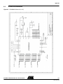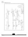
1
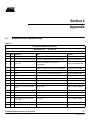
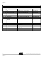
AT43DK355 USB Controller Development Kit for the AT43USB35X Family ........................................................................................................................... User Guide Version 1.0 Table of Contents Section 1 Introduction ........................................................................................... 1-1 1.1 1.2 1.3 1.4 Features ....................................................................................................1-1 Device Support .........................................................................................1-1 Documentation ..........................................................................................1-2 Free Downloads ........................................................................................1-2 Section 2 Getting Started...................................................................................... 2-1 2.1 Electrostatic Warning ................................................................................2-1 2.2 Unpacking the System ..............................................................................2-1 2.3 System Requirements...............................................................................2-1 2.4 Software Requirements.............................................................................2-1 2.5 Connecting the Hardware .........................................................................2-2 2.6 CD-ROM Contents ....................................................................................2-2 2.6.1 USB Wizard Utility ..............................................................................2-2 2.6.2 Code Base Directory ..........................................................................2-3 2.6.3 Application Example ...........................................................................2-4 2.6.4 In-System Programming Tool.............................................................2-4 2.6.5 Atmel USB HID Demo Utility ..............................................................2-4 2.6.6 Binary Files for Uploading ..................................................................2-5 2.7 Checking the Hardware.............................................................................2-5 Section 3 Hardware Description ........................................................................... 3-1 3.1 3.2 3.3 3.4 3.5 3.6 3.7 3.8 3.9 3.10 3.11 3.12 3.13 3.14 3.15 3.16 AT43DK355 USB Controller Dev. Kit User Guide LEDs (LD0 to LD7)....................................................................................3-1 5x2 Header JP14 ......................................................................................3-1 8 DIP Switch SW1.....................................................................................3-1 5x2 Header JP16 ......................................................................................3-2 DB 25 Female Parallel Port Connector J4 ................................................3-2 8-pin IC Socket U4 ....................................................................................3-2 Variable Resistor R15 ...............................................................................3-2 2x2 Header JP9 ........................................................................................3-2 Programmable Logic Device U2 ...............................................................3-2 5x2 Header JP5 and 2x2 Header JP6.......................................................3-2 4x2 Header General Purpose I/O PORT A/JP1 ........................................3-2 4x2 Header General Purpose I/O PORT B/JP2 ........................................3-2 4x2 Header General Purpose I/O PORT D/JP4........................................3-3 2x2 Header General Purpose I/O JP3 ......................................................3-3 2x2 Header JP8. .......................................................................................3-3 2x2 Header JP13 ......................................................................................3-3 i 3429C–USB–7/04 Table of Contents 3.17 3.18 3.19 3.20 3.21 3.22 3.23 3.24 2x2 Header JP11 ......................................................................................3-3 Solid State Power Switch U3 ....................................................................3-3 2x2 Header JP12 ......................................................................................3-3 Header GND TP1 and TP2 .......................................................................3-4 Header JH1 ...............................................................................................3-4 USB External Downstream Port J2 and J3 Connectors............................3-4 USB Upstream Port J1 Connector ............................................................3-4 Programmable Microcontroller U1 ............................................................3-4 Section 4 SEEPROM Loader................................................................................ 4-1 4.1 4.2 Setting Up the Board.................................................................................4-1 Loading Code............................................................................................4-1 Section 5 Technical Support................................................................................. 5-1 Section 6 Appendix............................................................................................... 6-1 6.1 6.2 AT43USB355 Bill of Materials (BOM) .......................................................6-1 AT43DK355 Schematics ...........................................................................6-3 Section 7 Change Log .......................................................................................... 7-1 ii 3429C–USB–7/04 AT43DK355 USB Controller Dev. Kit User Guide Section 1 Introduction Congratulations on your purchase of the AT43DK355 USB Development Kit. The AT43DK355 is a complete starter kit and development system for Atmel's AT43USB35x family of AVR® based USB microcontrollers (MCUs). It provides all of the necessary hardware and firmware components to facilitate rapid prototyping and firmware development of the AT43USB35x applications. 1.1 Features The AT43DK355 Development Kit consists of the following: Development Board for the AT43USB35x USB MCUs featuring – An AT43USB355 full-speed USB controller programmable as a compound device, a hub only device or a function only device – One internal and two external downstream HUB ports – 1 Kbytes on-chip program SRAM – 24 Kbytes of program memory – Parallel interface to PC for In-System firmware programming – 8 push buttons and 8 LEDs for general use – Pin header connectors for access to all available GPIO pins Hardware design files (schematics and PCB layout) USB 2.0 compliant USB firmware library USB Wizard firmware source code generation utility In-System Programming tool Complete User Guide 1.2 Device Support The AT43DK355 Development Kit and the accompanying software tools are intended to support firmware development and prototyping for the AT43USB35x family of USB function controllers, including the – AT43USB355 – AT43USB353M – AT43USB351M AT43DK355 USB Controller Dev. Kit User Guide 1-1 3429C–USB–7/04 Introduction Binary compatibility across the AT43USB3xx family ensures that only one set of development tools (development kit, compilers, etc.) is needed for all of the AT43USB3xx based applications. Firmware written for one member of the family can be re-used for another member without modification as long as only features available on both parts are used. 1.3 Documentation The AT43DK355 Development Kit is accompanied by the following two documents: – AT43DK355 User Guide – USB Wizard User Guide Atmel recommends its customers read the AT43DK355 User's Guide prior to reading the USB Wizard User Guide. 1.4 Free Downloads 1-2 3429C–USB–7/04 The latest version of the USB Wizard can be found in the USB section of the Atmel web site at http://www.atmel.com. Please refer to the same section for up-to-date information on new USB product announcements, software releases and tool upgrades. AT43DK355 USB Controller Dev. Kit User Guide Section 2 Getting Started 2.1 Electrostatic Warning The AT43DK355 Development Board is shipped in protective anti-static packaging. The board must not be subjected to high electrostatic potentials. A grounding strap or similar protective device should be worn when handling the board. Avoid touching the component pins or any other metallic elements. 2.2 Unpacking the System The AT43DK355 Development Kit is supplied with the following: – AT43DK355 Development Board – 2-meter Fully Rated USB Cable – Male-male DB25 Parallel Cable – Atmel USB CD-ROM with Software and Documentation Please contact your local Atmel distribution or e-mail [email protected] if any of the aforementioned items is missing from the package. 2.3 System Requirements The minimum hardware and software requirements are: – 486 processor (Pentium® is recommended) – 128 MB RAM – 10 MB free hard disk space – Windows® 98/2000/ME/XP – Parallel printer port 2.4 Software Requirements The following third party software are needed to access and modify the documents and source code in the CD-ROM: – OrCAD Capture® from www.orcad.com for the .dsn file – IAR or GNU C Compiler for the sample C source code – Microsoft® Word from www.microsoft.com for the .doc files – Acrobat® Reader® from www.adobe.com for the .pdf files – Winzip® from www.winzip.com to open the .zip files AT43DK355 USB Controller Dev. Kit User Guide 2-1 3429C–USB–7/04 Getting Started 2.5 Connecting the Hardware Atmel has taken great care in creating a reliable demonstration kit for its customers. The AT43DK355 Development Board is USB bus powered and requires no external power supplier. In order to ensure proper operation, the supplied components in the kit must be used in the setup shown in Figure 2-1. Atmel does NOT recommend substitution of these components. Connect the AT43DK355 Development Board as follows: 1. Verify that Jumper JP8 and Jumper JP11 are closed. 2. Connect the USB cable from J1 Series B USB receptacle on the Development Board to the USB Series A receptacle on the PC. 3. Connect the DB25 parallel cable from J4 on the Development Board to the parallel port on the PC. Figure 2-1. Connection to the AT43DK355 USB Cable Target USB Device J3 Target USB Device J2 J1 2.6 CD-ROM Contents DB25 Parallel Cable J4 AT43DK355 Development Board The CD-ROM has a top directory \355_evx\ where x indicates the version of the firmware. All the directory paths used in this User Guide fall under this top directory. There are three major subdirectories: – BOARD: hardware design documentation – Docs: datasheets, tutorial, and user guide – USBWizard: USB Wizard software tool and examples 2.6.1 USB Wizard Utility USB Wizard utility is a GUI based development tool that facilitates rapid USB application development for the AT43USBxxx family of AVR USB controllers. It allows the user to generate firmware templates in ANSI C for USB and AVR® peripherals with few clicks of the mouse. This utility is located in \USBWizard\USBWizard direcotry. This directory contains the USB Wizard executable file and other dependencies files. 2-2 3429C–USB–7/04 AT43DK355 USB Controller Dev. Kit User Guide Getting Started Please refer to the Readme file on the release CD for the installing instructions. The USB Wizard executable file is supported on Windows® 98/2000/ME/XP. Source code generated by the USB Wizard cannot be programmed directly into the onboard SEEPROM device. It must be compiled and linked first. The USB Wizard currently supports IAR and GCC compilers. Refer to the Atmel “USB Wizard User Guide” and “USB Wizard: Application Examples and Demos” for detailed descriptions of this utility. Figure 2-2. USB Wizard Application Window 2.6.2 Code Base Directory This is the directory where all code base needed by USB Wizard are taken from. The name of this directory is \USBWizard\Codebase. There are two main groups of code base within this directory. The first one is IARbase, which provides necessary code for IAR. The second one is GCCbase which contains the code for the GCC compiler. The following is a brief summary of directory tree of this code base. Code base | |------------ IARbase | | | |------ AT43USB35x | |------ AT43USB326 | |------ AT43USB325E | |------------ GCCbase | |------ AT43USB35x |------ AT43USB326 |------ AT43USB325E AT43DK355 USB Controller Dev. Kit User Guide 2-3 3429C–USB–7/04 Getting Started 2.6.3 Application Example The application examples are also included within this package. They are located in \USBWizard\Examples\ directory. This directory contains USB Wizard configuration files (*.usw files) and the corresponding C files for application examples. There are five subdirectories in this directory: 1. PWM_ADC_GPIO 2. OCR1A 3. OCR1B 4. SPI 5. Hub_Disabled 2.6.4 In-System Programming Tool The SEEPROM Loader allows developers to program the SEEPROM device through the standard parallel port. The tool is located in \USBWizard\ISP\ directory. Please refer to the Readme file for installation instructions. Please read Section 4 of this document or Section 3 of Atmel USB Wizard: Application Examples and Demos on how to use this utility. Figure 2-3. SEEPROM Loader Tool Window 2.6.5 Atmel USB HID Demo Utility This tool, located in \USBWizard\Demo_Utility\, is purposed to exercise the functionality of application examples. To install it, copy and paste the executable file in this directory to the desired location. How to use this utility will be fully explained in Atmel USB Wizard: Application Examples and Demos especially for example 1 (PWM, ADC, and GPIO). 2-4 3429C–USB–7/04 AT43DK355 USB Controller Dev. Kit User Guide Getting Started Figure 2-4. USB HID Demo Utility Window 2.6.6 Binary Files for Uploading The ready-made programmable binary files for loading are located on the CD-ROM in the \USBWizard\Binary\ directory. The files have extension *.hex. They are located under three subdirectories: 1. OCR1A 2. OCR1B 3. PWM_ADC_GPIO 2.7 Checking the Hardware The Development Board comes with a preprogrammed application. Connect the USB upstream port of the Development Board to the downstream port of the host (i.e.: PC). Then, check its existence in the Device Manager of the System Control Panel window. If the Development Board is working properly, it should show up in the PC as a HID compliant device. Another way to check the proper functioning of the board is to connect a USB device such as a mouse to one of the downstream USB hub ports on the Development Board. The Development Board is functioning properly if the mouse is detected by the PC. AT43DK355 USB Controller Dev. Kit User Guide 2-5 3429C–USB–7/04 Getting Started 2-6 3429C–USB–7/04 AT43DK355 USB Controller Dev. Kit User Guide Section 3 Hardware Description The following hardware description explains the Development Board in detail. The Development Board schematic can be found in Section 6.2. Figure 3-1. Simple Block Diagram of the DK355 Board 3.1 LEDs (LD0 to LD7) The AT43DK355 Development Kit includes 8 green LEDs. The anode pin of each LED is connected to the VBUS, through a resistor. 3.2 5x2 Header JP14 Each pin of this header is connected to the cathode pin of each LED. To turn on the LED, JP14 is pulled low. 3.3 8 DIP Switch SW1 Positioning a switch to ON causes the corresponding SWx pin on JP16 to be pulled low while releasing it will result in a high impedance state. AT43DK355 USB Controller Dev. Kit User Guide 3-1 3429C–USB–7/04 Hardware Description 3.4 5x2 Header JP16 These headers are connected to one of each DIP switch. 3.5 DB 25 Female Parallel Port Connector J4 The parallel port connector, J4, is used for In-System Programming to upload firmware from the PC to the SEEPROM U4. A DB25 male-to-male parallel cable is supplied to connect the J4 connector to the PC parallel port. Further description on downloading code to the SEEPROM is available in Section 3 of the USB Wizard: Application Examples and Demos document for the AT43USB355. 3.6 8-pin IC Socket U4 The SEEPROM device is plugged to this 8-pin socket to store programming memory. This board is supplied with an Atmel 25HP256 SEEPROM. 3.7 Variable Resistor Variable resistor R15 can be used to adjust voltage of the VREF pin of the AT43USB355 in order to test the Analog to Digital Converter (ADC) feature. This resistor produces R15 variable voltage levels that can be fed to the ADC input header (JP6 and JP5). The voltage produced from this resistor can be accessed from pin 4 of header JP9. 3.8 2x2 Header JP9 To use the ADC, a reference voltage must be applied to the VREF pin of the AT43USB355. This reference voltage can be fixed at the CEXT voltage by setting a jumper between pin 1 and pin 2, or the reference voltage can be adjustable (by adjusting R15) by setting a jumper between pin 3 and pin 4 of J9. JP9: 1-2 VREF = CEXTA (jumper installed by default) 3-4 VREF is adjustable 3.9 Programmable Logic Device U2 This Development Board uses the ATF16V8CZ Electrical Erasable PLD for In-System Programming and for downloading data from SEEPROM to AT43USB355. 3.10 5x2 Header JP5 and 2x2 Header JP6 JP5 are input pins for ADC channels zero to seven and JP6 are for ADC channels eight to eleven. 3.11 4x2 Header General Purpose I/O PORT A/JP1 Accessing PORTA externally can be performed at this header. A number is assigned to each pin header, “0” to “7”, corresponds to the port's pin number. 3.12 4x2 Header General Purpose I/O PORT B/JP2 Accessing PORTB externally can be performed at this header. A number is assigned to each pin header, “0” to “7”, corresponds to the port's pin number. 3-2 3429C–USB–7/04 AT43DK355 USB Controller Dev. Kit User Guide Hardware Description 3.13 4x2 Header General Purpose I/O PORT D/JP4 Accessing PORTD externally can be performed at this header. A number is assigned to each pin header, “0” to “7”, corresponds to the port's pin number. 3.14 2x2 Header General Purpose I/O JP3 External access to PF0 to PF3 is available at this header. These pins are used to download programing from the SEEPROM to the AT43USB355E as soon as power is applied to the board. Once firmware is downloaded, the AT43USB355 drives PF0 high while leaving PF1-PF3 as a general purpose I/O. PF3 also has an alternate function as the ICP input capture pin for the Timer/Counter1. 3.15 2x2 Header JP8. This header will take effect whenever the Pulse Width Modulation (PWM) feature is enabled. The 43USB355E has two PWM features, PWM1 and PWM2, which are outputting to PD5 (PORT D pin 5) and PD6 (PORT D pin 6). Installing jumpers to these pins, connect PWM outputs to the base of transistors, Q2 and Q4 to amplify PWM signals. If the PWM feature is disabled, PD5 and PD6 will be available as general purpose I/Os. JP8: 1-2 PD5 = PWM1 (jumper installed by default) 3-4 PD6 = PWM2 (jumper installed by default) 3.16 2x2 Header JP13 There are three pins marked as PWM1, PWM2 and VBUS at this header. The PWM1 and PWM2 pins can be used to drive DC motors. The pin marked VBUS is the 5V USB upstream port voltage. 3.17 2x2 Header JP11 This Development Board provides a ganged power switching and overcurrent sensing features for two downstream USB ports. This feature occupies PD0 and PD1 and requires the use of the Micrel MIC2026-2BM solid state power switch. The PD0 and PD1 must be connected to this power switch by installing a jumper to this header. If this system is not used, PD0 and PD1 will be available as general purpose I/Os. JP11: 1-2 PD1 = Downstream USB power switching enable (jumper installed by default) 3-4 PD0 = Overcurrent protection enable (jumper installed by default) 3.18 Solid State This device manages the ganged power switching system and overcurrent sensing feaPower Switch U3 ture. This board uses the Micrel MIC2026-2BM. 3.19 2x2 Header JP12 The pin marked as VBUS provides USB downstream port voltage. If the application requires the use of the Micrel MIC2020-2BM for power switching and overcurrent protection, no jumpers are installed on JP12; otherwise, a jumper is needed between pin 1 and pin 2 of JP12. JP12: 1-2 Connected = No power switching Unconnected = Power switching (default) 3-4 No connection AT43DK355 USB Controller Dev. Kit User Guide 3-3 3429C–USB–7/04 Hardware Description 3.20 Header GND TP1 and TP2 This pin provides ground voltage reference. 3.21 Header JH1 VICP input capture pin for the Timer/Counter1 feature. 3.22 USB External Downstream Port J2 and J3 Connectors These connectors provide downstream connection to USB devices. There are 3 downstream ports. Port 1 is permanently used by embedded functions and is not visible. On this board, be aware that J3 corresponds to USB Port 2 of 43USB355E and J2 corresponds to USB Port 3 of 43USB355E. The power source of these ports is controlled by power switch U3. 3.23 USB Upstream Port J1 Connector This connector provides upstream connection to a host or to another hub. 3.24 Programmable Microcontroller U1 This board comes with the AT43USB355E microcontroller. 3-4 3429C–USB–7/04 AT43DK355 USB Controller Dev. Kit User Guide Section 4 SEEPROM Loader The SEEPROM Loader is an Atmel software tool used to program the SEEPROM via generic parallel ports. This section describes the tool briefly. 4.1 Setting Up the Board Before starting the In-System Programming, please verify the following configurations: 1. The EEPROM is properly plugged to U4. 2. No any jumpers installed on JP6. 3. The upstream USB port is connected to the PC. This connection is needed for board's power source. 4. J4 connector is connected to the parallel port on the PC. 4.2 Loading Code After setting up the board, the next process is loading the firmware. This development kit comes with application firmware that has been properly formatted for the SEEPROM. The files are located in the subdirectories under the \USBWizard\Binary\ directory. 1. Open SEEPROM Loader.exe. It is located at in \USBWizard\ISP\ directory on CD-ROM. Figure 4-1. SEEPROM Loader Application AT43DK355 USB Controller Dev. Kit User Guide 4-1 3429C–USB–7/04 SEEPROM Loader The following error message may appear in a pop-up window indicating that an extra DLL file needs to be downloaded and installed. Figure 4-2. Error message of running SEEPROM_Loader.exe The SEEPROM loader uses the DriverLINXT parallel port driver DLPortIO.DLL which provides the Win32 DLL hardware I/O functions. Windows® NT® and 2000 users also require the DLPortIO.SYS kernel mode driver. Both of these drivers are copyrighted Scientific Software Tools, Inc. (www.driverlinx.com). To download the drivers, follow the following steps: 1. Go to http://www.driverlinx.com/DownLoad/dnload.htm 2. Click on Windows 95/NT Port I/O Driver 3. Download the .exe file. 2. Before selecting the memory, click on Reset to bring the device to the Active reset state. Then select the memory from Memory Choice: list box. Figure 4-3. Selecting Memory Flash 4-2 3429C–USB–7/04 AT43DK355 USB Controller Dev. Kit User Guide SEEPROM Loader 3. Click on Write Flash button. Figure 4-4 will appear. Figure 4-4. Selecting the File 4. Locate the *.hex file to be downloaded, and then click Open to start downloading. If successful, a message box will be displayed stating that the download was a success. Select one of *.hex files which are located in the \USBWizard\Binary\ directory. 5. Once a successful upload has been completed, a message box will appear, as shown in Figure 4-5. 6. Click OK to close the message box. 7. Disconnect the DB25 parallel cable from the J4 connector, then disconnect and reconnect the board's USB upstream port to reset the evaluation board. Another way to rest the board is to click on the Reset to make the board stay in a Non-active reset state. And then, disconnect and reconnect the board's USB upstream port. Figure 4-5. A Successful Download 8. Clicking Exit will terminate the application. AT43DK355 USB Controller Dev. Kit User Guide 4-3 3429C–USB–7/04 SEEPROM Loader 4-4 3429C–USB–7/04 AT43DK355 USB Controller Dev. Kit User Guide Section 5 Technical Support For technical support, please e-mail [email protected] with the following information: – The revision number of the AT43DK355 Development Board – The version number of the USB Wizard – A detailed description of the problem Alternatively, fill out an online support form available in the Product Section of the Atmel web site at http://www.atmel.com. AT43DK355 USB Controller Dev. Kit User Guide 5-1 3429C–USB–7/04 Technical Support 5-2 3429C–USB–7/04 AT43DK355 USB Controller Dev. Kit User Guide Section 6 Appendix 6.1 AT43USB355 Bill of Materials (BOM) Table 6-1. AT43USB355 USB Microcontroller/Hub AT43USB355_EV3 Revision: 1.0 Bill Of Materials - November 19, 2002 Item Qty Reference Part Supplier 1 4 C1, C11, C12, C32 0.01 UF, cer 0805, Panasonic ECU-V1H103KBG Digikey PCC103BNCT-ND 2 7 C2, C3, C14, C16, C18, C24, C28 0.1 UF, cer 0805, Panasonic ECJ-2VB1E104K Digikey PCC1828CT-ND 3 9 C4, C6, C8, C15, C17, C19, C21, C33, C35 0.001 UF, cer 0805, Panasonic ECUV1H102KBG Digikey PCC102BNCT-ND 4 1 C5 0.33 UF, cer 0805, Panasonic ECJ-2YB1C334K Digikey PCC1817CT-ND 5 3 C7, C10, C34 2.2 UF, cer 0805, Panasonic ECJ-2YB0J225K Digikey PCC1851CT-ND 6 1 C20 4.7 UF, el A, Panasonic ECE-V1ES4R7SR Digikey PCE3065CT-ND 7 6 C22, C23, C26, C27, C30, C31 47 PF, cer 0603, Panasonic ECJ-1VC1H470J Digikey PCC470ACVCT 8 2 C29, C25 220 UF, el D, Panasonic ECE-V0JA221WP Digikey PCE3310CT-ND 9 1 JH1 Header 1x1 10 6 JP1, JP2, JP4, JP5, JP14, JP16 Header_5X2 Jameco 67820 923810R 11 7 JP3, JP6, JP8, JP9, JP11, JP12, JP13 Header_2X2 Jameco 115027 923804R 12 1 J1 USB-B, AMP 787780-1 Digikey 787780-1 13 2 J3, J2 USB-A, AMP 787616-1 Digikey 787616-1 14 1 J4 CONNECTOR, D-SUB .318RT 25P-F Jameco 15181, 1008-25S 15 8 LD1, LD2, LD3, LD4, LD5, LD6, LD7, LD0 LED, green Jameco 34606, XC209G 16 6 L2, L3, L4, L5, L6, L7 Ferrite Bead, Stewart HI1206N800R-00 Digikey 240-1010-1-ND 17 2 Q2, Q4 2N4401 Jameco 38421 AT43DK355 USB Controller Dev. Kit User Guide 6-1 3429C–USB–7/04 Appendix Table 6-1. AT43USB355 USB Microcontroller/Hub AT43USB355_EV3 Revision: 1.0 Bill Of Materials - November 19, 2002 Item Qty Reference Part Supplier 18 1 R1 100, 0805 Panasonic ERJ-6GEYJ101V Digikey P100ACT-ND 19 3 R2, R16, R17 1.5K, 0805 Panasonic ERJ-6GEYJ152V Digikey P1.5KACT-ND 20 6 R3, R4, R5, R6, R7, R8 27, 0805 Panasonic ERJ-6GEYJ270V Digikey P27ACT-ND 21 4 R9, R10, R11, R12 15K, 0805 Panasonic ERJ-6GEYJ153V Digikey P15KACT-ND 22 1 R13 1M, 0805 Panasonic ERJ-6GEYJ105V Digikey P1.0MACT-ND 23 3 R14, R18, R19 100K, 0805 Panasonic ERJ-6GEYJ104V Digikey P100KACT-ND 24 1 R15 50K Potentiometer Jameco 94721 X201R50K 25 8 R20, R22, R24, R25, R26, R27, R28, R29 470, 0805 Panasonic ERJ-6GEYJ471V Digikey P470ACT-ND 26 6 R30, R31, R32, R33, R34, R39 0, 0805 Panasonic ERJ-6GEY0R00V Digikey P0.0ACT-ND 27 4 R35, R36, R37, R38 2.2K, 0805 Panasonic ERJ-6GEYJ222V Digikey P2.2KACT-ND 28 1 SW1 SW DIP-8, DS-08-G-01-BL Jameco 38842 29 1 U1 AT43USB355-AC Atmel 30 1 U2 ATF16V8CZ TSSOP Atmel 31 1 U3 MIC2026-2BM Micrel 32 1 U4 AT25HP256-10PC, PDIP 8-Pin socket Jameco 51570 33 1 Y1 6.000 MHz Thru-Hole Crystal, CTS ATS060 Digikey CTX405-ND 6-2 3429C–USB–7/04 AT43DK355 USB Controller Dev. Kit User Guide Appendix 6.2 AT43DK355 Schematics Figure 6-1. AT43DK355 Schematic (1 of 5) AT43DK355 USB Controller Dev. Kit User Guide 6-3 3429C–USB–7/04 Appendix Figure 6-2. AT43DK355 Schematic (2 of 5) 6-4 3429C–USB–7/04 AT43DK355 USB Controller Dev. Kit User Guide Appendix Figure 6-3. AT43DK355 Schematic (3 of 5) AT43DK355 USB Controller Dev. Kit User Guide 6-5 3429C–USB–7/04 Appendix Figure 6-4. AT43DK355 Schematic (4 of 5) 6-6 3429C–USB–7/04 AT43DK355 USB Controller Dev. Kit User Guide Section 7 Change Log Doc. Rev. Comments 3429C • AT43DK355 USB Controller Dev. Kit User Guide Information Change: Complete revision of Section 3. 7-1 3429C–USB–7/04 Change Log 7-2 3429C–USB–7/04 AT43DK355 USB Controller Dev. Kit User Guide Atmel Corporation 2325 Orchard Parkway San Jose, CA 95131, USA Tel: 1(408) 441-0311 Fax: 1(408) 487-2600 Regional Headquarters Europe Atmel Sarl Route des Arsenaux 41 Case Postale 80 CH-1705 Fribourg Switzerland Tel: (41) 26-426-5555 Fax: (41) 26-426-5500 Asia Room 1219 Chinachem Golden Plaza 77 Mody Road Tsimshatsui East Kowloon Hong Kong Tel: (852) 2721-9778 Fax: (852) 2722-1369 Japan 9F, Tonetsu Shinkawa Bldg. 1-24-8 Shinkawa Chuo-ku, Tokyo 104-0033 Japan Tel: (81) 3-3523-3551 Fax: (81) 3-3523-7581 Atmel Operations Memory 2325 Orchard Parkway San Jose, CA 95131, USA Tel: 1(408) 441-0311 Fax: 1(408) 436-4314 RF/Automotive Theresienstrasse 2 Postfach 3535 74025 Heilbronn, Germany Tel: (49) 71-31-67-0 Fax: (49) 71-31-67-2340 Microcontrollers 2325 Orchard Parkway San Jose, CA 95131, USA Tel: 1(408) 441-0311 Fax: 1(408) 436-4314 La Chantrerie BP 70602 44306 Nantes Cedex 3, France Tel: (33) 2-40-18-18-18 Fax: (33) 2-40-18-19-60 ASIC/ASSP/Smart Cards 1150 East Cheyenne Mtn. Blvd. Colorado Springs, CO 80906, USA Tel: 1(719) 576-3300 Fax: 1(719) 540-1759 Biometrics/Imaging/Hi-Rel MPU/ High Speed Converters/RF Datacom Avenue de Rochepleine BP 123 38521 Saint-Egreve Cedex, France Tel: (33) 4-76-58-30-00 Fax: (33) 4-76-58-34-80 Zone Industrielle 13106 Rousset Cedex, France Tel: (33) 4-42-53-60-00 Fax: (33) 4-42-53-60-01 1150 East Cheyenne Mtn. Blvd. Colorado Springs, CO 80906, USA Tel: 1(719) 576-3300 Fax: 1(719) 540-1759 Scottish Enterprise Technology Park Maxwell Building East Kilbride G75 0QR, Scotland Tel: (44) 1355-803-000 Fax: (44) 1355-242-743 Literature Requests www.atmel.com/literature Disclaimer: Atmel Corporation makes no warranty for the use of its products, other than those expressly contained in the Company’s standard warranty which is detailed in Atmel’s Terms and Conditions located on the Company’s web site. The Company assumes no responsibility for any errors which may appear in this document, reserves the right to change devices or specifications detailed herein at any time without notice, and does not make any commitment to update the information contained herein. No licenses to patents or other intellectual property of Atmel are granted by the Company in connection with the sale of Atmel products, expressly or by implication. Atmel’s products are not authorized for use as critical components in life support devices or systems. © Atmel Corporation 2004. All rights reserved. Atmel® and combinations thereof, and AVR ® are the registered trademarks of Atmel Corporation or its subsidiaries. Pentium® is the registered trademarks of Intel Corporation. Microsoft® Word and Windows ® 98/2000/ME/XP are the registered trademarks of Microsoft Corp. Acrobat ® Reader ® is the registered trademarks of Adobe Systems Inorporated. Winzip ® is the registered trademarks of Winzip Computing Inc. OrCAD Capture ® is the registered trademarks of Cadence Design Systems, Inc. Other terms and product names may be the trademarks of others. Printed on recycled paper. 3429C–USB–7/04 /xM