1
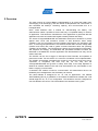
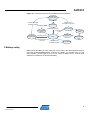
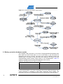
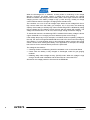
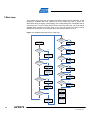
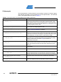
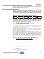
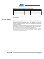
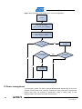
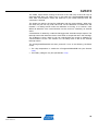
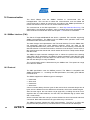
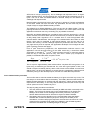
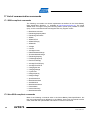
AVR474: ATAVRSB202 Firmware User's Guide
Features
• Provides all needed safety measures for a lithium-ion battery
- Voltage
- Current
- Temperature
• High accuracy voltage and current measurements
• Communication
- TWI/SMBus 1.1 compatible
- Command set based on Smart Battery specification
• HMAC-SHA2 authentication
8-bit
Microcontrollers
Application Note
1 Introduction
This document describes an example Smart Battery implementation using the
Atmel® ATAVRSB202 evaluation kit. The implementation demonstrates how to use
the Atmel ATmega16HVB/32HVB to gain optimal safety and measurement
accuracy for a lithium-ion rechargeable battery pack. All code is available under a
limited license agreement to allow for easy evaluation and further development.
The SB202 targets smart batteries with two, three, or four lithium-ion and lithiumpolymer cells in series. The product is based on the same firmware source code,
but compiled differently for each configuration. The SB202 hardware for evaluation
of the ATmega16HVB/32HVB device and the SB202 executable file are available
as the Atmel ATAVRSB202 evaluation kit.
Figure 1-1. Atmel SB202 evaluation kit hardware.
Rev. 8237A-AVR-03/11
2 Overview
The main purpose of a Smart Battery implementation is to protect the battery from
overcharging, over-discharging, and use outside its temperature and current limits. It
also estimates the battery’s remaining capacity, and communicates this to a
host/application.
Often, smart batteries offer a method for authenticating the battery. The
authentication makes it possible to ensure that only a compatible battery is used for
an application. This allows the manufacturer of the application to guarantee that the
application will work as intended with regard to battery lifetime and safety.
The Atmel ATmega16HVB/32HVB has dedicated autonomous hardware to protect
against short circuit and excessive currents in both directions. Other safety
conditions, such as cell voltage level and operating temperature, are handled by the
CPU. To ensure good performance, the coulomb-counter ADC and the voltage ADC
(CCADC and VADC) are used to gather accurate information about the operating
conditions of the battery. The CPU/firmware collects and processes this information,
and responds accordingly. The dedicated and specialized hardware modules are
described in the datasheet, and this application note demonstrates how they can be
used to their best.
The CCADC can be set to trigger an interrupt at fixed intervals, and operates in
power-save mode. For this reason it is used as a timebase in this implementation.
The CCADC accumulates (averages) the current for one second, and every time a
conversion is completed, the main loop will run one loop and the
ATmega16HVB/32HVB will go back to sleep. How deep it can sleep depends on
whether all modules started in the main loop are finished or not, and whether or not
there is ongoing communication.
A hardware TWI module is used for communication. All transmissions have to be
initiated by the host/application, but the battery can answer.
The Atmel SB202 is designed for 2s, 3s, and 4s applications. The #define
“BATTPARAM_CELLS_IN_SERIES” in the header file determines whether the code
should target the 2s, 3s, or 4s configuration. The hardware must be configured for
use with different cell counts. This is described in the hardware user’s guide.
2
AVR474
8237A-AVR-03/11
AVR474
Figure 2-1. Overview of how the Atmel SB202 firmware operates.
Storage Mode
(Power-Off)
Charger Detect
Enter Storage Mode
command received
Initialization Failed
Initialization
Voltage very low
(less than 2.5V per cell)
Initialization Finished
Respond to
communication
Command parsed
Communication
from host
Scan voltage
New CCADC
result
FETs disabled
forever
Sleep
Battery Current
Protection triggered
Check battery
safety
Update Gas
Gauging
Enable/Disable
FETs
FETs disabled
3 Battery safety
Making sure the battery is not a safety risk for the user is the most important task for
the Atmel ATmega16HVB/32HVB. A lithium-ion battery can become very hot and
even explode if overcharged or if too much current is drawn from it, and so good
protection is needed for a commercial battery.
3
8237A-AVR-03/11
Figure 3-1. Overview of the battery safety system.
3.1 Battery protection hardware module
The hardware battery protection on the Atmel ATmega16HVB/32HVB disables both
FETs when too much current flows in or out of the battery. It has three limits for
discharging and two for charging. The limits can be set to different currents and
reaction times. This allows a very fast short-circuit detection, but allows for lower
charge/discharge spikes without cutting supply to the host/application. Table 3-1
shows an example of how the three discharge limits can be set up.
Table 3-1. Example timings for battery protection.
Current exceeds
Duration for discharge FET to be disabled
2A
20ms
3A
2ms
6A
125µs
In this implementation, the lowest discharge current limit (called discharge highcurrent protection) is disabled to allow faster discharges during testing. The
parameters are stored in the EEPROM and used to configure the module at startup.
4
AVR474
8237A-AVR-03/11
AVR474
Multiple charge over-/high-current protections in a row indicate a malfunctioning
charger. In that case, the charge FET is disabled and will not be enabled again until a
discharge current higher than standby is detected. That way, the battery is protected
even if disconnected from the charger and connected again.
3.2 Firmware-based battery protection
The firmware-based battery monitoring of the operating conditions is protecting the
battery from over-voltage, under-voltage, and hazardous temperatures.
3.2.1 Current
Because the battery lifetime is decreased by high charge and discharge currents, the
current flowing in/out of batteries should be limited to a reasonable level, which can
be determined according to the battery characteristics data and a realistic application
scenario. It might also be desired to use more sophisticated current limitation
schemes/algorithms than simple thresholds. This is left up to the end user to
implement.
3.2.2 Temperature
Very high or very low operating temperatures reduce the lifetime of the battery, and
moreover, high temperature can also be a sign that the battery is damaged.
Therefore, it is common practice to disable charging/discharging when the
temperature is outside a certain temperature range. This is a good idea both for
general safety and battery lifetime. This implementation checks the temperatures
every four seconds (to minimize active time and power consumption). This is
considered sufficient for most batteries, as rapid thermal changes are not expected.
By default, cell temperature monitoring is disabled because no thermistor is soldered
on the Atmel SB202 at assembly. Thermistors are, however, provided with the SB202
kit. See Section 11.3 for more information. Instead, the internal Atmel
ATmega16HVB/32HVB temperature reference is assumed to be the same as the cell
temperature.
If the temperature is too high or too low, either the charge or discharge FET will be
disabled, depending on in which direction the current is flowing. It will not be enabled
again until the temperature is within the allowed limits.
If the internal temperature of the ATmega16HVB/32HVB is outside the operating
limits (-20°C to 80°C), the ATmega16HVB/32HVB will turn itself off and the FETs will
automatically be disabled.
All the temperature limits for the battery are stored in the EEPROM.
3.2.3 Voltage
By checking the voltage, the battery can protect itself from overcharging and overdischarging. Both of these conditions reduce the battery lifetime and are a safety risk.
Therefore, when a charge current is flowing, the cells are continuously checked for
over-voltage, and similarly, while discharging, they are checked for under-voltage.
When the voltage is too high, the charge FET will be disabled. It will not be enabled
again until a discharge current higher than standby is flowing. The protection works
the same for the discharge FET; after an under-voltage condition, the discharge FET
will not be enabled again until a charge current is detected.
5
8237A-AVR-03/11
When the discharge FET is disabled, its body diode is conducting in the charge
direction. However, the diode causes a voltage drop that reduces the voltage
difference between the charger and the battery stack, which again causes a reduced
charging current. If the battery voltage is high (~3.55V and up), virtually no charge
current will flow when the charger is charging with a standard 4.2V.
This condition can occur if the cell voltage drops below the low-voltage limit due to
high current drawn from the battery (for example, 3C). In this case, the remaining
capacity of the battery is still fairly high. When the discharge FET is disabled by hitting
the low-voltage limit, the battery cell will recover and the voltage will increase. The
voltage can increase from 2.7V to 3.6V, which is high enough to limit the charging.
To handle this scenario, the discharge FET is enabled if the battery voltage is above
a given threshold or if a charging current is detected (a few mA is enough).
If the voltage drops very low (for example, 0.2V below minimum operating voltage for
the cell), the Atmel ATmega16HVB/32HVB turns itself off to limit further discharging
of the battery. To avoid shutting down on short discharge spikes such as due to high
outrush current when inserting the battery in an application, for example, the voltage
has to be low for two seconds before power-off is performed.
The voltage is also used for:
• Checking whether cell balancing should be activated or not on the Atmel SB202
• Check when the battery is fully charged or discharged; useful for gas gauging
modules
• Disabling deep under-voltage recovery (DUVR) mode. When the voltage is high
enough, DUVR mode is disabled, and the firmware can control the FETs
All limits for the voltage protection are stored in the EEPROM.
6
AVR474
8237A-AVR-03/11
AVR474
4 Battery parameters/settings
Most battery parameters are stored in the EEPROM for easy reconfiguration. Those
values are in “physical” units; that is, mA, minutes, etc. Internally the Atmel SB202
uses other units to reduce computation complexity to a minimum. Therefore, at
startup, some parameters in the EEPROM are converted into other units and stored
in the SRAM.
Changes to some settings that require that the code be recompiled affect more than
just a value in the EEPROM. Most obvious are settings for the number of cells and
the availability of external temperature sensors.
All parameters and settings are located and commented in the
battery_pack_parameters.h/c files. Battery characteristics data are stored in the
firmware module that uses them; for example, cc_gas_gauging and
voltage_based_SoC.
7
8237A-AVR-03/11
5 Clocks and calibration
The Atmel ATmega16HVB/32HVB’s internal fast RC oscillator is used as the system
clock. It runs at a nominal frequency of 8MHz, but the system clock prescaler should
be fused to 1/8 for the SB202, resulting in a system clock with a frequency of 1MHz.
The fast RC oscillator varies over temperature. However, this can be avoided by
calibrating the fast RC at runtime with the use of the slow RC oscillator, whose
frequency can be determined as a linear function of temperature. This makes it
possible to calibrate the fast RC oscillator with sufficient accuracy to have reliable
UART communication. The calibration is run every time the chip temperature has
changed by 2°C.
When the slow RC period is known (calculated), it is known how many fast RC ticks
should occur during that period for it to be running at 1MHz. When calibrating, the
number of fast RC ticks during eight slow RC periods is counted, and the calibration
register is adjusted until the number is as correct as the adjustment allows for. The
calibration register is only adjusted one step at a time to avoid changing the
frequency too much.
5.1 Real-time counter
There is no need for an accurate real-time counter (RTC) on the Atmel SB202. Realtime is only used for knowing approximately when a number of minutes have passed,
and is not used for any calculations.
The RTC is clocked by the ULP RC oscillator through the CCADC conversion time.
Since the actual ULP RC period can be calculated through slow RC, it is possible to
improve the accuracy of the RTC if needed.
8
AVR474
8237A-AVR-03/11
AVR474
6 Initialization flow (after reset)
During initialization, all peripheral and firmware modules are configured, calibrated,
and prepared for operation. Upon the very first startup (that is, power-up after
programming), CCADC offset adjustment is also performed. The initialization
sequence is listed below.
1. Set up the watchdog, and check if too many watchdog resets have occurred. If it
has, it indicates a major problem, and the battery should be disabled. (Nothing is
done in this implementation.)
2. Disable unused peripherals and pins to reduce the power consumption.
3. Check that the battery parameters and signature row is correct (CRC16). If they
are not, the part can be measuring wrong values and have wrong limits for
battery protection. So, the battery should be disabled if the checks fail. (Nothing is
done in this implementation.)
4. Calibrate the bandgap. If it fails, the readings from the ADC modules cannot be
trusted, and, therefore, the battery will be disabled.
5. Initialize the hardware battery protection module.
6. Set up the VADC module with gain coefficients and offsets from the signature
row.
7. Values to convert between internal units from the CCADC to mA/mAh are
calculated from the shunt resistor value stored in the EEPROM.
8. Some frequently used limits from the battery parameters are converted to internal
units to avoid doing that calculation every second.
9. The VADC runs one scan of all available inputs to have values for the first main
loop and also to check if the DUVR mode can be disabled.
10. If a serious failure has not occurred earlier in the initialization process, the
CCADC and coulomb counter gas gauging modules are configured. The
remaining capacity for the CC-based gas gauging is set by using the state of
charge (SoC) from the voltage-based gas gauging. It is, however, marked as
inaccurate and updated as soon as the voltage-based gas gauging has an
accurate estimation.
11. If it is the very first start-up, it will measure the CCADC offset. This process takes
up to 30 seconds.
12. Finally, the communication is initialized and global interrupts enabled before
entering the main loop.
9
8237A-AVR-03/11
7 Main loop
The purpose of the main loop is to gather and react to data from the interrupts. It runs
through all available data and checks that all are within the limits. If errors are
discovered during charging or discharging, the corresponding FET is disabled and an
error flag is set. If no error flags are set at the end of the main loop, the FETs will be
enabled again. Because the main loop is run once per second, the FETs will be
disabled for a minimum of one second when the firmware detects an error.
Figure 7-1. Simplified flowchart for the main loop.
Fast RC
calibration
needed?
Reset watchdog
timer
New current
available?
No
Cell
temperature
ready?
Yes
No
No
Yes
Run fast RC
calibration
Yes
Calculate
temperature and
check limtis
Start voltage ADC
conversions
Cell 1 voltage
ready?
Yes
Handle cell1
voltage
Byte received on
communication?
No
Yes
Handle received
byte
If a whole
command have
been received,
parse that
No
Cell 2 voltage
ready?
Yes
Handle cell2
voltage
No
Cell 3 voltage
ready?
Yes
Handle cell3
voltage
Was a new
current available?
Yes
Update the RTC
No
Handle the new
current
No
Cell 4 voltage
ready?
Yes
Handle cell4
voltage
No
Check all flags to
see if the FETs
can be enabled
Core temperature
ready?
No
10
Yes
Calculate
temperature and
check limits
Decide what
sleep mode that
is possible
Enter sleep
AVR474
8237A-AVR-03/11
AVR474
The hardware battery protection module prevents the FETs from being enabled within
one second after a battery protection event (caused by too high current) has been
triggered. Because the current protection is handled by hardware, the main loop
doesn’t have to check for that before enabling the FETs.
11
8237A-AVR-03/11
8 Interrupts
The implementation is interrupt-based: All processing is based on interrupt triggers,
and interrupts (and flags) are an essential part of the implementation. The interrupts
used in the implementation are listed in Table 8-1.
Table 8-1. Interrupts used in the Atmel SB202 Smart Battery application.
Interrupt source/function name
Description
Voltage regulator monitor interrupt
VREGMON_ISR()
Stores all interrupt settings for the various modules and enters powersave until the voltage regulator is okay again or CREG is empty. If the
voltage regulator is okay, restores the interrupts and continues operation.
See the Atmel ATmega16HVB/32HVB datasheet for a description of how
the voltage regulator monitor works
Watchdog timeout interrupt
WDT_Timeout_ISR ()
Only used by the voltage regulator monitor interrupt to wake the device
up and check if the voltage regulator is okay
Timer 0 output compare match interrupt
RCCAL_InputCapture_ISR()
Captures the number of fast RC clocks during one slow RC period. See
Chapter 5, Clocks and calibration, on page 8
Battery protection interrupt
BATTPROT_BatteryProtection_ISR()
Triggered when the hardware battery protection module disables the
FETs due to excessive currents or short circuit. Sets a flag, which is used
to alert the host. If it was an overcharge, it increases the number of times
this has happened to be able to detect a malfunctioning charger.
CCADC accumulating conversion complete interrupt
Ccadc_Acc_ISR()
If the CCADC is set to negative polarity, the result is negated; otherwise it
is just stored as is. The main loop will then process the result. If polarity
switching compensation (see Section 10.2) is activated, the
compensation is done here.
Voltage ADC conversion complete interrupt
VADC_ISR()
Flags that a channel or group of channels is complete. The main loop will
then process the result. If there are more channels to scan in the ongoing
sweep, sets the MUX and starts the VADC again. Otherwise turns the
VADC off.
TWI (SMBus) interrupt request
TWI_ISR()
Maintains the TWI (SMBus) state machine to implement the
communication
Timer 1 overflow interrupt
T1OVF_ISR( )
Provides timer tick for the code. The timeout period is 2.048ms
Timer 1 output compare match B interrupt
T1_COMPB_ISR()
Checks the hold time of the button pushed. After the hold time is larger
than the predefined period, the LED will be lit to indicate the volume of
capacity or the error code. The LED on time is set at LED_ON_TIMEOUT
Timer 1 output compare match A interrupt
T1CMPA_ISR()
Reduces the LED on time until it is zero, and then turn off the LEDs
Pin change interrupt 0
PCINT0_ISR
Checks the button input, and will trigger if there is a pin change on the
button. This enables the timers to show status codes on the LEDs
12
AVR474
8237A-AVR-03/11
AVR474
9 FET control
If an error occurs that requires the current flow to be cut, the FET will get disabled
immediately and an error flag will be set. The FET will not be enabled again until all
errors have disappeared; that is, all error flags are cleared.
The flags are divided into different variables in the code, but only the flag name is
used here.
Table 9-1. FET control conditions.
Flag name
Clearing conditions
Description
CriticalConditonDetected
Will never get cleared
Set if the bandgap or VADC can’t be calibrated/initialized, and
will keep both FETs disabled all the time
ChecksumFailure
Will never get cleared
Set if either the signature or EEPROM battery parameters
CRC is wrong. Is not done in this implementation, but the
battery should be disabled if the checksums are wrong
InDUVR
Cleared when DUVR mode is
disabled
Set at start-up and if the code detects that the DUVR mode
has been enabled again. Will prevent both FETs from being
enabled, but the DUVR has control over the charge FET so
charging is possible
SystemIsInStandby
Cleared if the current is higher
than the active current threshold
in either direction
Set if the current is less than the active current threshold. By
default, that is 10mA
ReoccuringChargeProtection
Cleared when an active discharge Set if a too-high charge current is detected too many times in a
current is detected
row, which indicates a malfunctioning charger. Will disable the
charge FET when set and prevent it from being enabled again
until cleared
ChargingProhibited
Cleared when an active discharge Set if a too-high voltage is detected. Will prevent the charge
current is detected
FET from being enabled while set
DischargingProhibited
Cleared when an active charge
current is detected
Set if a too-low voltage is detected. Will prevent the discharge
FET from being enabled while set
VoltageTooHigh
Cleared if the last voltage was
below the maximum for all cells
Set if the last voltage was too high for any cell. Disables the
charge FET
VoltageTooLow
Cleared if the last voltage was
above the minimum for all cells
Set if the last voltage was too low for any cell. Disables the
discharge FET
CellTemperatureTooHigh
Cleared if the last temperature
reading is below the maximum
limit
Set if any cell temperature (or the internal temperature
reference of the Atmel ATmega16HVB/32HVB if no thermistor
is connected) is too high. Will disable either the charge or
discharge FET when set, depending on which direction the
current is flowing. Will prevent both FETs from being enabled
while set
CellTemperatureTooLow
Cleared if the last temperature
reading is above the minimum
limit
Set if any cell temperature (or the internal temperature
reference of the ATmega16HVB/32HVB if no thermistor is
connected) is too low. Will disable either the charge or
discharge FET when set, depending on which direction the
current is flowing. Will prevent both FETs from being enabled
while set
13
8237A-AVR-03/11
10 CCADC
The result from the CCADC is used to check the current level, compute the average
current over one minute (approximated to save memory), and compute the
accumulate charge that has flowed in and out of the battery. Only the accumulated
result from the CCADC is used when checking limits and accumulating charge. The
CCADC is set to a one-second conversion time and to trigger an interrupt when
conversion is complete. That way it can also be used to update the RTC. The actual
timing will depend on the temperature, but as described in Chapter 5, Clocks and
calibration, page 8, the RTC does not need to be very accurate.
The actual conversion time is important when accumulating current for counting the
charge that has flowed through the battery. The CCADC is clocked by the slow RC
oscillator, and its period can be calculated from the internal temperature reference of
the Atmel ATmega16HVB/32HVB and the slow RC temperature predication value that
is stored in the signature row. The cc_gas_gauging module is responsible for
accumulating the capacity and compensates for the actual slow RC period.
If polarity switching is enabled, the CCADC accumulating conversion complete
interrupt is responsible for storing the result so that it is always positive for a charging
current and negative for a discharging current.
When a new current result is ready from the CCADC, it is passed to the
battery_current_monitoring module by the main loop, where it is added to the oneminute average current. The average is calculated as shown in Equation 10-1.
Method for calculating average current. The scaling is used to improve accuracy
and is removed when the average is returned.
NOTE
An exponential filter is used to estimate a one-minute moving average current. This is
done to save memory, as a one-minute moving average is very SRAM-consuming.
Battery_current_monitoring also gives easy access to the current and offset
calibrated current for other modules that need it.
Equation 10-1. Method for calculating average current.
124 * Old average + 4 * current * 2 n
128
n = AVERAGE_CURRENT_SCALING (default value: 4)
New average =
10.1 CCADC offset
The CCADC has a certain offset. When accumulating charge, it can be cancelled out
by switching polarity at a fixed interval. But as it is possible to measure the offset, it’s
nice to use that to correct the measurement when it’s used as momentary current. It
helps the most on low current when checking whether the battery is in standby mode
or not.
The offset is measured the first time the battery is started and takes 20-30 seconds,
during which both FETs will be disabled. It discards the first sample after every switch
and compares the average of the other samples between positive and negative
CCADC polarity. Half the difference is the offset, and that can then be added or
removed (depending on polarity setting) to later measurements to get a more correct
value.
14
AVR474
8237A-AVR-03/11
AVR474
Switching polarity too often is not a good idea because the first accumulating
conversion after a polarity switch is not correct.
10.2 Challenges with polarity switching
The ACC conversion from the CCADC is calculated from the average of 256
instantaneous conversions by hardware (one-second conversion time). But every
time the polarity is switched, the first two to three instantaneous current conversions
are wrong. The first one is completely off, the second quite wrong and the third is
almost always correct, and if not, then only slightly wrong.
Figure 10-1. Example ICC samples before and after a polarity switch.
This is caused by settling time in the CCADC, which requires two to three ICC
conversions to settle. In the example in Figure 10-1, the error for a one-second
conversion time and a constant current of -185 would be:
error =
254 * 185 + (−140 + 101) − (256 *185)
% = −0.86%
256 * 185
To remove the problem as much as possible, the two or three samples after the
switch should be removed from the ACC result for that second and replaced with an
average of the ICCs before and after them.
To do that, the part has to wake up three or four extra times after a polarity switch to
read the ICC results, and that adds active time and, therefore, power consumption. It
also adds complexity and code space.
The Atmel SB202 takes a simpler approach that still removes most of the error. The
sum of the two samples after the switch is small compared to one ICC sample, so
they are already considered “removed.” And instead of adding the average of the ICC
readings around them, only the ICC sample from just before the polarity switch is
used. As that sample is available when switching the polarity, practically no runtime is
added.
With the same assumptions as in last error calculation, the error will now be:
error =
NOTE
(254 *185 + (−140 + 101) + 2 *182) − 256 *185
% = 0.095%
256 *185
In Figure 10-1, the results are not polarity compensated, so the result from before the
switch is negated before using it in the error calculation.
Since the ACC result has the same range for different conversion times, the result is
downscaled by the hardware. Therefore, the ICC result also has to be downscaled
before it is added to the ACC result.
For different values of samples and downscale from Table 10-1, the ACC result is:
⎛ samples
⎞
ACC = ⎜ ∑ ICC [n]⎟ >> downscale
⎜
⎟
⎝ n =1
⎠
15
8237A-AVR-03/11
Table 10-1. ICC samples for different ACC conversion times.
Conversion time
Samples
Downscale
1s
256
3
500ms
128
2
250ms
64
1
125ms
32
0
To replace the two “missing” ICC samples, the ICC sample from just before the switch
has to be divided by four (doubled and then scaled down three bits) before adding it
to the ACC result.
10.3 Shunt calibration
The result from the CCADC is the voltage drop over the external shunt resistor, which
on the Atmel SB202 has a value of 5mΩ, ±1%. The shunt resistance is used with the
result from the CCADC to calculate the current. As a calibration option, the shunt
value can be changed at runtime by sending a new shunt resistance value via the
communication interface.
An ammeter can be used to measure the exact current flowing in/out of the batteries.
This information can then be used to calculate what the shunt resistance really is.
This is described in more detail in the Atmel AVR491 application note.
The shunt resistance can be set between 4000µΩ and 16000µΩ using the
ShuntCalibration command (0x2A). Other values are possible, but require changes to
the code to avoid computational overflows.
16
AVR474
8237A-AVR-03/11
AVR474
11 VADC
The Atmel ATmega16HVB/32HVB MCU has a five-channel VADC for measuring cell
voltage, chip temperature, and cell/battery temperature. The chip temperature uses
an internal diode. External thermistors are required to measure the battery cell
temperatures.
Immediately after a CCADC ACC result is ready, a new VADC scan is configured and
started. This is to ensure that the data are ready when the main loop can process
them (because the VADC conversion takes a long time compared to the processing
of the data). Ideally, the VADC should only run while the CPU is busy processing
information. Otherwise, energy is wasted in noise-reduction-mode/idle-mode sleep, or
even active mode, just waiting for the conversion to complete. In reality, noisereduction sleep is used whenever it is required to wait for a conversion to complete.
Configuring the VADC scan means to set which channels should be sampled. It
depends on how many cells and thermistors are used. The cell voltages are sampled
every second, but temperatures are sampled only every fourth second as they do not
change that fast. The ADC input channels are scanned in the same order as they are
processed in the main loop. This is to ensure that the CPU can process data while
converting the next sample.
When one channel is finished, the VADC conversion complete interrupt routine sets a
data ready flag to notify the main loop. This allows the main loop to process, for
example, the result from cell one voltage while the VADC is sampling cell two voltage.
The interrupt routine advances to the next input channel in the scan (reconfigure the
VADC mux) or, if the scan is completed, turns off the ADC sample.
11.1 VADC calibration
To ensure optimum accuracy when using the VADC, all results must be corrected for
offset and gain error. The offset and gain compensation can be read from the HVB
signature row. Please refer to the datasheet for more details.
Equation 11-1. Offset and gain compensation of the VADC result.
ADCcompensated = ( ADCresult − ADCoffset ) ⋅ ADCgain
; (downscaled by 214 )
11.2 Chip temperature
To calculate the chip temperature, the VADC result is multiplied by the VPTAT value
from the signature row and scaled down as described in the datasheet. Further, it is
multiplied by 10 to get results in 0.1K, as required according to the SBS specification.
All temperatures are stored in 0.1K.
NOTE
The VADC result for the internal temperature reference only requires gain
compensation. Offset compensation is not required.
11.3 Cell temperature
Because no thermistors (NTC) are soldered on the Atmel SB202 during assembly,
cell temperature reading (and processing) is disabled by default. Instead, the chip
temperature is assumed to be the same as the cell temperature when evaluating the
system temperature.
17
8237A-AVR-03/11
To use one or two thermistors, connect them as described in the Atmel AVR455
application note and change two defines in battery_pack_parameters.h (search for
CELLTEMPERATURE_INPUTS and read the comments just above it).
To convert the VADC result to mV, the result has to be offset calibrated, multiplied
with a gain coefficient, and then scaled down. The downscaling is chosen to
maximize accuracy so the VADC module by default returns 200*voltage in mV.
Equation 11-2. How to calculate voltage on the VADC according to the datasheet.
ADCmV =
1 ( ADCresult − ADCoffset ) ⋅ ADC gain
⋅
10
16384
Equation 11-3. How the Atmel SB202 calculates the scaled voltage from the VADC
result.
ADCscaled _ mV =
( ADCresult − ADCoffset ) ⋅ ADC gain
8192
The thermistors supplied with the SB202 are Mitsubishi RH16-3h103f, and the NTC
firmware module in the ntc_rh163h103f.c file converts the scaled voltage from the
VADC module to Kelvin or degrees Celsius. To use another NTC, other data used by
the firmware module have to be used.
11.4 Cell voltage
To get the real voltage from the VADC result, an offset has to be added and the result
multiplied with a gain coefficient and then scaled down, as written in the datasheet.
This conversion between the VADC result and the actual voltage is calculated only
once per conversion; later use of the cell voltage thus does not spend time converting
the VADC result to volts.
18
AVR474
8237A-AVR-03/11
AVR474
12 Gas gauging
Gas gauging is estimating how much capacity and runtime is left in the battery. The
Atmel ATmega16HVB/32HVB can achieve high accuracy gas gauging by means of
its very accurate VADC and CCADC. The great storage capability in flash, SRAM,
and EEPROM allows the use of accurate battery models.
The Atmel SB202 uses a combination of voltage- and coulomb-counter-based gas
gauging. The voltage-based gas gauge is used to initialize the remaining capacity,
which the coulomb counter then will increase/decrease during use.
12.1 Gas gauging strategy on the SB202
At start-up, the voltage-based gas gauging estimates the state of charge (SoC) using
an approximation of the internal resistance of the battery. The remaining capacity is
calculated from that SoC and from the latest full-charge capacity stored in the
EEPROM. This provides a reasonable initial estimate of the SoC and remaining
capacity, though it is not as accurate as the estimate will be when the open-circuit
voltage (OCV) is measured, or when the battery has been charged to full capacity
once. For this reason, a flag is used to indicate that the SoC/remaining capacity is
“inaccurate” and that a better estimation should be performed as soon as possible.
The SoC from the voltage-based gas gauging module is considered accurate when
the current has been below the standby current limit for 30 minutes or more.
(Threshold for standby current is specified in firmware and stored in EEPROM.) The
first time this happens after start-up, the remaining capacity is updated and is no
longer flagged as inaccurate.
Remaining capacity is updated every second by the coulomb counter, and it is used
to calculate all the information the SB202 can provide to the host/application.
Because the end-of-discharge voltage is reached sooner when high currents are
drawn from the battery, the calculation of the runtime to empty takes the current level
into account. The calculation uses characterization data for the specific battery cell
type to determine how the available capacity changes at different current levels
compared to when using only a very small current. Ideally, the characteristic data
should be updated as the battery gets older, as the battery characteristics change
slightly over time, but this is not offered in this application.
12.2 Voltage-based gas gauging
Voltage-based gas gauging works quite well to determine the SoC from the open
circuit voltage (OCV, that is, at no or low current). But as soon as “more” current is
flowing, the battery’s internal resistance effects reduce the terminal voltage. The
resistance changes with temperature, SoC, and battery age, which makes it
challenging to accurately estimate the SoC from only the OCV.
Two other problems with voltage-based gas gauging are:
• It only gives the state of charge in percents and no indication of the capacity of the
battery, which makes it hard to give an accurate runtime for the battery
• When the current stops, the voltage does not immediately return to the OCV. How
long it will take depends on the battery, but generally it takes about 30 minutes
19
8237A-AVR-03/11
However, the combination of OCV-based estimation and coulomb-counting-based
estimation provides a good overall estimation that is not very sensitive to
temperature, aging, etc.
12.3 Coulomb counter gas gauging
A coulomb counting approach keeps track of how much current is charged into the
battery and discharged from it. It is very accurate, even at high currents. The
disadvantage of the coulomb-counting-based gas gauging is that it can measure
changes only. This means that it does not offer information about the absolute charge
level, and, therefore, an initial charge state is also required.
When doing coulomb-counter-based gas gauging, the current charge/remaining
capacity has to be estimated using a voltage-based approach at start-up and also
possibly after a long time in standby. If the initial voltage-based SoC estimate is
wrong, the coulomb-counter-based estimate will also be wrong. It can, however,
calibrate itself when reaching a fully discharged and fully charged state.
By using a coulomb counter, the full charge capacity can be updated as the battery
gets older with the following method:
It is known when the battery is fully charged and fully discharged, so how much
charge has been used between these states is the full-charge capacity. A full charge
on a lithium-ion cell is reached when the charge current has dropped low enough,
often down to the range of 10 - 15mA. Full discharge is a bit trickier to gauge, as the
end-of-discharge (EoD) voltage will be reached before the battery is actually empty
when discharging with high currents because of the internal resistance. So the EoD
has to be reached at a low enough current for it to be a full discharge.
The fact that the battery will typically never get fully discharged because the
host/application shuts down represents a challenge when trying to estimate the
remaining charge and runtime to empty.
20
AVR474
8237A-AVR-03/11
AVR474
13 Battery characterization data
The Atmel SB202 needs a table for SoC versus OCV, a table for how much less
capacity is available at higher currents, and, optionally, but recommended, the full
charge capacity.
The SB200 can be used together with the PC demonstration software to log all data
that is available from the SB202, and can, therefore, be used as a platform for
characterizing batteries.
13.1 Full-charge capacity
The full-charge capacity of the battery is often different from the design capacity. The
battery will update the full-charge capacity if it determines it is not correct.
The full-charge capacity as well as the design capacity should be the amount of
capacity available at a very low current; that is, about 10mA.
This parameter is stored in the EEPROM in the battery_pack_parameters module.
13.2 State of charge vs. voltage
The voltage-based gas gauging uses a table of the OCV at different SoCs from 0% to
100%. The SB202 does a linear interpolation between the two closest points in the
table, so the SoCs don’t have to be at a fixed interval. This allows having fewer
values between 70% and 30%, where the OCV is almost linear for most batteries,
and more values near the end of the discharge, where the voltage changes a lot
more.
NOTE
The SB202 requires having values at exactly 100% and 0%.
The table is stored in the voltage_based_SoC module.
13.3 Remaining capacity compensation
Because of the internal battery resistance and the fact that it increases towards the
end of a discharge, it is not possible to get as much capacity out of a battery at higher
currents. Therefore the SB202 needs to know how much less capacity is available at
different currents to know how much longer the battery can sustain the current load.
The SB202 supports an arbitrary number of currents in the remaining capacity
compensation table and will interpolate between the two closest. If the current is
higher than the highest value in the table, it will predict the compensation value by
using the two highest values.
The internal resistance of the battery varies with the temperature, but this is not yet
supported by this implementation.
21
8237A-AVR-03/11
14 Cell balancing
When using multi-cell battery packs, it is important that they are balanced with regard
to cell voltage to get maximum capacity from the battery pack. To understand why,
understanding the lithium-ion charge cycle is required:
The charger will charge with either the maximum charge current or the maximum
charge voltage. In the beginning of the charge cycle, when the battery is almost
empty, the charge current will reach the maximum limit. Hence, when the battery
starts building a certain charge level, the charge voltage will increase and eventually
reach the voltage limit (typically 4.2V per Li-ion cell), and thus be the limiting factor for
the charger. An intelligent charger will not allow the charge voltage of the battery pack
to increase above this level, and, as a result, the charge current will decrease. These
two stages are called constant current charge and constant voltage charge.
The problem is that when using two cells, the charger will have the voltage limit at
8.4V. If one cell is more charged than the other, that is, in misbalance, it will reach the
maximum charge voltage sooner than the other cell. In this case, the most charged
cell could have reached 4.2V, while the least charged is at 4.1V. In this situation, the
voltage of the battery stack is 8.3V and the charger will not notice that one of the
battery cells has reached its maximum charge voltage. The charger will continue the
constant current charge and the voltage will continue to increase until the battery
pack voltage is 8.4V. This means that the most charged cell may reach 4.25V, which
is the absolute maximum voltage for safety reasons, and the Atmel SB202 will disable
the charge FET.
When this happens, neither cell is fully charged as a lithium-ion cell should be
charged at maximum charge voltage for quite some time. If the problem arises, there
is a high risk that the cell misbalance will continue to get worse and worse. As a
result, if the cells are highly misbalanced, the charger will not be able to operate as
intended and the battery pack will not be charged to its maximum capacity.
The solution used by the SB202 is to discharge the most charged cell until the voltage
difference between the cells is low enough. The threshold, called
BATTPARAM_MISBALANCE_VOLTAGE_THRESHOLD, is stored in EEPROM in the
battery_pack_parameters module.
As misbalancing is primarily an issue while charging a battery pack, cell balancing is
active only while charging the battery. During discharging, activation of cell balancing
would have limited effect. Be aware that if two highly misbalanced cells are operating
together, it may take several charge-discharge cycles to balance the cells.
In the Atmel ATmega16HVB/32HVB, the balancing FETs are internal, and no external
FETs are required. The filtering resistors limit the maximum balancing current that
can flow through the internal FETs. It should be noted that as the balancing FETs are
internal, the dissipated power will affect the temperature of the chip. Depending on
the maximum balancing current, the internal temperature can be raised up to 30
degrees in room temperature. The cell balancing should, therefore, be disabled at a
certain level if the external temperature NTC is not used to monitor the battery cell
temperatures.
For 2s battery packs, the cell balancing algorithm is as simple as balancing the top
most cell of the two cells. For 3s and 4s battery packs, the algorithm is more complex.
The ATmega16HVB/32HVB can balance up to two cells at a time as long as they are
not adjacent to each other. For example, cells one and three can be balanced at the
same time, but not cells one and two. For a 3s and 4s implementation, the cell with
22
AVR474
8237A-AVR-03/11
AVR474
the highest voltage will be balanced, and if the second highest cell voltage is not an
adjacent cell, this will also be balanced.
The algorithm will not balance the third highest voltage cell if the second one is
adjacent to the highest cell and can’t be balanced. This would only make the lowest
cells more unbalanced, and are, therefore, not balanced until they reach the voltage
of the highest cells.
In addition, in order to increase the charging efficiency, the algorithm permits the cell
balancing to take place only if the remaining state of charge is larger than 80%.
23
8237A-AVR-03/11
Figure 14-1. Flowchart of cell balancing for a four-cell application.
START
Order cells by voltage
(cell1 = lowest, cell4 = highest)
Find voltage differences relative to the
lowest cell (diff_h, diff_m)
Is diff_h >
mb_threshold?
YES
Is cell4 physically
next to cell3?
YES
NO
NO
Turn on balancing
for cell4
Is diff_m >
mb_threshold?
NO
YES
Turn on balancing
for cell3
END
15 Power management
To save battery power, the Atmel ATmega16HVB/32HVB should sleep as much as
possible in power-save mode. However, it should not enter power-save if a peripheral
module that does not operate in power-save mode is being used. In this
implementation, that means the VADC and the timers.
24
AVR474
8237A-AVR-03/11
AVR474
The VADC might still be running at the end of the main loop if the main loop is
executed faster than one VADC scan. In that case the ATmega16HVB/32HVB will
enter ADC noise-reduction mode and wake up by the VADC interrupt when the
conversion is finished.
The timers are used by the fast RC calibration and the communication. When they
are used, the part can only enter idle mode. As the calibration is initiated from the
firmware, it is always known when the calibration is running. It is, however, more
difficult to determine if the communication is active, as this is caused by an external
event.
A transmission is started by a start bit that triggers the external interrupt request. The
interrupt routine then starts the timer to know when to sample the bits in the message.
The challenge is that a start bit can be received after the check to determine if
communication is active. The solution is to set sleep mode to idle in the external
interrupt routine.
The ATmega16HVB/32HVB will enter power-off if one of the following conditions
occurs:
• The chip temperature is outside the ATmega16HVB/32HVB limit (see Section
3.2.2)
• The battery voltage is very low (see Section 3.2.3)
25
8237A-AVR-03/11
16 Communication
The Atmel SB202 uses the SMBus interface to communicate with the
host/application. The host has to initiate the communication, and the SB202 will
communicate only if asked. On some errors, according to the SMBus specification, a
timeout mechanism on the SCL line is used to detect the errors.
The command set is the SBS specification 1.1 from http://www.sbs-forum.org. The
specification is not followed completely, some commands are not fully supported, and
some reserved commands are used. See Chapter 17 for the list of commands.
16.1 SMBus interface (TWI)
The Atmel ATmega16HVB/32HVB has built-in, optimized TWI controller supporting
SMBus implementation. The SB202 only has SMBus slave operation mode: slave
transmitter mode and slave receiver mode.
The state changes are implemented in the TWI serial interrupt. From the SB202 side,
one transaction starts from slave address matching, which can wake up the
ATmega16HVB/32HVB from power-save mode. But for the following command and
data transmission in the same transaction, the device must be kept in active mode or
idle mode because the data arrival cannot awake devices from a sleep mode deeper
than idle mode.
The SB202 accepts received messages with or without the packet error-checking
code (PEC). When transmitting, the SB202 is always prepared to send the PEC after
sending the message. If the host does not want a PEC, it can send a NACK signal
after the last data byte to notify the SB202.
The communication speed is determined by the SMBus host. The speed can range
from 10kHz to 100kHz.
16.2 Protocol
The SBS specification uses the SMBus protocol. The SB202 is compatible with
SMBus specification 1.1. According the SBS specification, the battery pack address
is fixed at 0x16.
The SB202 supports four different types of messages:
• Read word
• Write word
• Read block
• Write block
A word command always has two bytes of data, and a block command always has 32
bytes, which is different from the SBS block commands, which have variable lengths.
After the start signal, the host sends a byte (eight bits), including the seven mostsignificant bits, the slave address, and the LSB, the read/write flag (0 means write
and 1 means read).
All the command codes are one byte, and are divided into word commands and block
commands. Both sides should have to agree what every command is.
The SB202 firmware supports the PEC implementation. The PEC is a CRC8 with
polynomial 0x8D (CRC8-CCITT) calculated from the command and all data bytes.
26
AVR474
8237A-AVR-03/11
AVR474
16.2.1 Read commands
On read commands, the host first writes the command to the Atmel SB202, and then
restarts the communication with the read flag. After that, the slave places the data
bytes on the SDA line one by one.
16.2.2 Write command
On write commands, the host sends the command byte and data bytes consecutively
to the SB202. After SB202 receives one byte, it replies with a one-bit ACK or nonACK signal. After the last data byte, the SB202 sends out an ACK signal to ask for a
PEC byte from the host. But if the host does not support the PEC function, it will send
a stop (P) signal, from which the slave can know the message is finished.
Figure 16-1. A read word command.
1
7
1 1
8
Master S Slave Address Wr
Slave
11 1
CMD
7
1 1
8
1
P R/S Slave Address Rd
A
A
8
1
A
A Data Byte
8
11
A
/A P
Data Byte
PEC
Figure 16-2. A write word command.
1
Master
7
1
1
S Slave Address Wr
Slave
8
1
CMD
8
1
Data Byte
A
8
1
8
Data Byte
A
1
1
PEC
A
P
A
/A
Figure 16-3. A read block command.
1
7
1 1
Master S Slave Address Wr
Slave
8
11 1
CMD
A
7
1 1
8
1
P R/S Slave Address Rd
A
8
1
A
A Data Byte0
8
1 1
A
… Byte 31
/A P
PEC
Figure 16-4. A write block command.
1
Master
Slave
7
1
1
S Slave Address Wr
8
1
CMD
A
8
1
Data Byte0
A
8
1
… Data Byte31
A
8
1 1
PEC
A
P
/A
16.2.3 Errors
If errors occur during the communication, the SB202 can extend the clock low on the
SCL line for more than 25ms. And after that, the SB202 can release the TWI line and
reset the TWI controller. The errors include:
• Wrong command returned by the SB202
• Frame error on data sent from the SB202
• PEC incorrect on data sent from the SB202
16.3 Authentication
The SB202 contains both an AES encryption algorithm and a SHA256-based HMAC
that can be used for challenge-response authentication. It allows the host to make
sure the connected battery is a model it is compatible with.
Both algorithms cannot be used at the same time, and the decision must be made at
compile time using two defines, AUTH_USE_AES and AUTH_USE_HMAC_SHA2.
27
8237A-AVR-03/11
AES uses a 16-byte (128-bit) key, and a challenge and response size of 16 bytes.
HMAC-SHA256 uses a 32-bytes (256-bit) key, and challenge and response size of 31
bytes. The use of AES and HMAC-SHA2 is identical except for the difference in
challenge and response size.
Both the battery and the host have to know the key in advance. Typically, all batteries
of the same model will have the same key preloaded, and the host may have a
couple of keys to support different battery models.
The default key for HMAC-SHA256 is “This is a long key for HMAC-SHA2.” The key
preprogrammed into the SB202 at assembly for AES is “You cannot pass!” But a real
application should not use a key consisting only of printable characters.
Both AES and HMAC-SHA256 are considered secure and are approved by, among
others, the NSA. No known attack (other than brute-force) is known for either one (as
of May 2008). Both algorithms run in constant time to avoid timing-based sidechannel attacks. Nevertheless, the strength of the authentication also relies on other
factors, which may be exploited in side-channel attacks, such as how the key is
stored in the memory, how the challenge response is performed, and much more. If a
very high security level is required, the application developer is encouraged to learn
good cryptology practice and apply it.
From a pure brute-force perspective, the authentication methods used in this
application note will be quite strong: On the AES 128-bit key, a brute-force attack
127
38
would take, on average, 2 (1.7*10 ) tries to find the right key. If someone wants to
break the key in one year (32.6*106 sec), and uses 1 million (106) computers in
parallel, it will demand that each computer can do:
Keys
1.7 ⋅ 10 38
=
= 5.2 ⋅ 10 24 key tries / sec
sec ⋅ computers 32 .6 ⋅ 10 6 ⋅ 10 6
This is equal to approximately 5200 million-million complete AES encryptions of 16
bytes using a 128-bit key per nanosecond. So, even with a good portion of luck, one
should not expect to identify the key within a fair amount of time based on brute force
attacks. Still, it is left to the designer to ensure that the cryptographic method used is
sufficiently strong for the desired purpose, and that it is used with best practices.
16.3.1 Authentication procedure
The host first has to ask what model the battery is to figure out which key to use. The
next step is to send random data to the battery. The battery then executes the AES or
HMAC-SHA256 algorithm on the data with the shared key. When the host reads the
response from the battery, it can verify that the battery has used the correct key and
can be quite sure it is the model it says it is.
The step-by-step procedure is as follows:
1. The host sends the authenticate command (an SBS write block command) to the
battery. The first byte is always 0x01 in this implementation (it is used by the
battery to know when a new challenge has arrived). After that, 16 bytes of
random data should be sent for AES and 31 bytes for HMAC-SHA256.
2. The battery then runs the algorithm on the received data. Note that HMACSHA256 also includes the status byte (as the first byte in the data) in the
calculations, so when verifying the response, the host also has to do that. It also
means that the message length used when padding in the SHA256 algorithm
should be calculated from a challenge length of 32 bytes.
28
AVR474
8237A-AVR-03/11
AVR474
3. The host sends the authenticate command again to read the changed data, but
this time as an SBS read block command. The first byte is a status byte,
(described in Table 16-1) and the rest is the response. For HMAC-SHA256, the
last byte of the response has to be truncated to fit in the 32-byte block message.
4. The host then verifies the data from the battery and checks that the algorithm was
run with the correct key
Table 16-1. Read authentication status byte.
Status byte
Description
0x01
Authentication has not started yet
0x02
Authentication has started, but not finished
0x04
Authentication is finished
0x08
An error occurred
16.3.2 Importance of random data
It is very important that the host does not send the same challenge for every
authentication. If it does, a battery can hard-code the response and won’t have to
know the key, rendering the authentication useless for determining if a compatible
battery is connected. The same issue applies if only a few different data combinations
are used.
The best way to protect against this sort of attack is to send pseudo-random data
concatenated with some unique data for each host/application. The unique data can,
for example, be a serial number. Much more information about this can be found on
the Internet and in books about cryptology. Search for “replay attack.”
29
8237A-AVR-03/11
17 List of communication commands
17.1 SBS-compliant commands
The following commands are almost implemented as defined in the Smart Battery
Data Specification Revision 1.1, available at http://www.sbs-forum.org. The Atmel
SB202 does not support using and returning data in power (mW) instead of current
(mA), so the commands that should support both only support current.
•
•
•
•
•
•
•
•
•
•
•
•
•
•
•
•
•
•
•
•
•
•
•
•
•
•
•
•
•
ManufacturerAccess
RemainingCapacityAlarm
RemainingTimeAlarm
AtRate
AtRateToFull
AtRateToEmpty
AtRateOK
Voltage
Current
AverageCurrent
RelativeStateOfCharge
AbsoluteStateOfCharge
RemainingCapacity
FullChargeCapacity
RunTimeToEmpty
AverageTimeToEmpty
AverageTimeToFull
ChargingCurrent
ChargingVoltage
CycleCount
DesignCapacity
DesignVoltage
SpecificationInfo
ManufacturerDate
SerialNumber
ManufacturerName
DeviceName
DeviceChemistry
ManufacturerData
17.2 Non-SBS-compliant commands
Most of the following commands exist in the Smart Battery Data Specification, but
they are implemented a bit differently in the SB202. Some new commands are also
used, either with the optional SBS commands or reserved commands.
30
AVR474
8237A-AVR-03/11
AVR474
BatteryMode
0x03
Read word.
The bits defined and described in SBS are used, but they are not set to their default values (as
the SB202 doesn’t support the default settings) and changing them is not possible.
Some reserved bits are replaced with cell balancing information and FET status.
Bit
Description
15
CAPACITY_MODE
Set to 0 – “Report in mA or mAh”
14
CHARGER_MODE
Set to 1 – “Disable broadcasts of ChargingVoltage and ChargingCurrent” as the
SB202 cannot initiate communication
13
ALARM_MODE
Set to 1 – “Disable AlarmWarning broadcast” as the SB202 cannot initiate
communication
12
BALANCING_CELL3
Set when cell 3 is being discharged to keep the cells balanced
11
BALANCING_CELL2
Set when cell 2 is being discharged to keep the cells balanced
10
BALANCING_CELL1
Set when cell 1 is being discharged to keep the cells balanced
9
PRIMARY_BATTERY
Set to 0 – “Battery operating in its secondary role”
8
CHARGE_CONTROLLER_ENABLED
Set to 0 – “Internal Charge Control Disabled”
7
CONDITION_FLAG
Set to 0 – “Battery OK”
6
BALANCING_CELL4
Set when cell 4 is being discharged to keep the cells balanced
5
DUVRD from FCSR
Is set to the deep under-voltage recovery disabled bit from the FET control and
status register
4
CPS from FCSR
Set to the current protection status bit from the FET control and status register
3
DFE from FCSR
Set to the discharge FET enabled bit from the FET control and status register
2
CFE from FCSR
Set to the charge FET enabled bit from the FET control and status register
1
PRIMARY_BATTERY_SUPPORT
Set to 0 – Function not supported
0
INTERMAL_CHARGE_CONTROLLER
Set to 0 – Function not supported
31
8237A-AVR-03/11
Temperature
0x08
Read word
This should return the battery pack temperature. The SB202 will return the chip temperature in
0.1 Kelvin. TemperatureNTC1/TemperatureNTC2 can be used for getting the battery
temperature
MaxError
0x0C
This command is not supported
RemainingCapacity
0x0F
Read word
According to the specification, this should return the remaining capacity at 0.2C discharge
current. The SB202 will return the remaining capacity at the average current
BatteryStatus
0x16
Read word.
This command is basically implemented as specified in SBS, except that reserved bits are
used and the error codes are not supported.
32
Bit
Description
15
OVER_CHARGED_ALARM
Controlled by the chargingProhibited flag
14
TERMINATE_CHARGE_ALARM
Controlled by the voltageTooHigh flag
13
VREGMON_TRIGGERED
Reserved bit in SBS, is set if the voltage regulator monitor triggered since the last
time BatteryStatus was read. It is cleared when read
12
OVER_TEMP_ALARM
Controlled by the cellTemperatureTooHigh flag
11
TERMINATE_DISCHARGE_ALARM
Is set when remaining capacity is below a defined limit
(SBS_TERMINATE_DISCHARGE_LIMIT) and cleared when a charge is detected.
Recommended to use REMAINING_CAPACITY_ALARM instead, as it is
configurable at runtime
10
BATTERY_PROTECTION_TRIGGERED
Set if the battery protection hardware module has disabled the FETs since the last
time this command was read. Will be cleared when read
9
REMAINING_CAPACITY_ALARM
Set if the remaining capacity is lower than the value set by the
RemainingCapacityAlarm command. Updated once every minute
8
REMAINING_TIME_ALARM
Set if AverageTimeToEmpty is less than the value set by the RemainingTimeAlarm
command. Updated once every minute
7
INITIALIZED
Controlled by be inverse of the criticalConditionDetected flag
Because both FETs will be disabled when that flag is set, the host/application can
only detect that criticalConditionDetected is set if it also is connected to a charger
AVR474
8237A-AVR-03/11
AVR474
6
DISCHARGING
Set if the current in the last second was a discharge
5
FULLY_CHARGED
Set when the battery is considered fully charged and cleared as soon as a
discharge current higher than standby is detected
4
FULLY_DISCHARGED
Set when there is no capacity left in the battery at all.
TERMINATE_DISCHARGE_ALARM and the remaining capacity/time alarm
functions can be used to get earlier warnings. Is cleared when
RelativeStateOfCharge is above 20%
3-0
Error Codes
Not supported
Authentication
0x24
Read and write block
Described in Section 16.3
ShuntCalibration
0x2A
Read and write word
Non-SBS command. Is used to set the shunt resistor value in EEPROM. The value is set in
micro-ohms and supports values between 4000 and 16000µΩ; however, no check is done on
the value. Reading this command can be used to ensure the write command was successfully
received
FETDisable
0x2B
Write word
Non-SBS command. This command can be used to individually force the charge and
discharge FETs to be disabled, which can be useful for demonstration and testing purposes. If
bit 0 is high in the word, the charge FET will be disabled and kept disabled until this command
is sent again with bit 0 low. Bit 1 works the same way for the discharge FET.
Note that this command cannot force the FETs to be enabled; it can only force them to be
disabled
StorageMode
0x2C
Write word
Non-SBS command. This command will force the ATmega16HVB/32HVB to enter power-off
mode. To make sure a power-off really is wanted, the word sent has to be 0xFADE, or this
command will do nothing
TemperatureNTC2
0x2D
Read word
Non-SBS command. If a second NTC is connected, this will return its temperature in 0.1
Kelvin. If no NTC is connected, 0 Kelvin is returned
33
8237A-AVR-03/11
TemperatureNTC1
0x2E
Read word
Non-SBS command. If the first NTC is connected, this will return its temperature in 0.1 Kelvin.
If no NTC is connected, 0 Kelvin is returned
VoltageCell4
0x3C
Read word
Returns the voltage over cell 4 in mV. If only three cells are used, it will return 0
VoltageCell3
0x3D
Read word
Returns the voltage over cell 3 in mV. If only two cells are used, it will return 0
VoltageCell2
0x3E
Read word
Returns the voltage over cell 2 in mV
VoltageCell1
0x3F
Read word
Returns the voltage over cell 1 in mV
34
AVR474
8237A-AVR-03/11
AVR474
18 Table of contents
Features ............................................................................................... 1
1 Introduction ...................................................................................... 1
2 Overview ........................................................................................... 2
3 Battery safety ................................................................................... 3
3.1 Battery protection hardware module ................................................................... 4
3.2 Firmware-based battery protection...................................................................... 5
3.2.1 Current ..........................................................................................................................5
3.2.2 Temperature .................................................................................................................5
3.2.3 Voltage..........................................................................................................................5
4 Battery parameters/settings............................................................ 7
5 Clocks and calibration..................................................................... 8
5.1 Real-time counter ................................................................................................ 8
6 Initialization flow (after reset) ......................................................... 9
7 Main loop ........................................................................................ 10
8 Interrupts ........................................................................................ 12
9 FET control ..................................................................................... 13
10 CCADC .......................................................................................... 14
10.1 CCADC offset .................................................................................................. 14
10.2 Challenges with polarity switching .................................................................. 15
10.3 Shunt calibration.............................................................................................. 16
11 VADC............................................................................................. 17
11.1 VADC calibration ............................................................................................. 17
11.2 Chip temperature............................................................................................. 17
11.3 Cell temperature .............................................................................................. 17
11.4 Cell voltage...................................................................................................... 18
12 Gas gauging ................................................................................. 19
12.1 Gas gauging strategy on the SB202 ............................................................... 19
12.2 Voltage-based gas gauging............................................................................. 19
12.3 Coulomb counter gas gauging ........................................................................ 20
13 Battery characterization data...................................................... 21
13.1 Full-charge capacity ........................................................................................ 21
13.2 State of charge vs. voltage.............................................................................. 21
13.3 Remaining capacity compensation ................................................................. 21
14 Cell balancing............................................................................... 22
15 Power management ..................................................................... 24
35
8237A-AVR-03/11
16 Communication............................................................................ 26
16.1 SMBus interface (TWI) .................................................................................... 26
16.2 Protocol ........................................................................................................... 26
16.2.1 Read commands ......................................................................................................27
16.2.2 Write command ........................................................................................................27
16.2.3 Errors ........................................................................................................................27
16.3 Authentication.................................................................................................. 27
16.3.1 Authentication procedure .........................................................................................28
16.3.2 Importance of random data ......................................................................................29
17 List of communication commands ............................................. 30
17.1 SBS-compliant commands .............................................................................. 30
17.2 Non-SBS-compliant commands ...................................................................... 30
18 Table of contents ......................................................................... 35
36
AVR474
8237A-AVR-03/11
Atmel Corporation
2325 Orchard Parkway
San Jose, CA 95131
USA
Tel: (+1)(408) 441-0311
Fax: (+1)(408) 487-2600
www.atmel.com
Atmel Asia Limited
Unit 01-5 & 16, 19F
BEA Tower, Milennium City 5
418 Kwun Tong Road
Kwun Tong, Kowloon
HONG KONG
Tel: (+852) 2245-6100
Fax: (+852) 2722-1369
Atmel Munich GmbH
Business Campus
Parkring 4
D-85748 Garching b. Munich
GERMANY
Tel: (+49) 89-31970-0
Fax: (+49) 89-3194621
Atmel Japan
9F, Tonetsu Shinkawa Bldg.
1-24-8 Shinkawa
Chou-ku, Tokyo 104-0033
JAPAN
Tel: (+81) 3523-3551
Fax: (+81) 3523-7581
© 2011 Atmel Corporation. All rights reserved. / Rev.: CORP072610
®
®
®
Atmel , Atmel logo and combinations thereof, AVR , AVR logo, and others are registered trademarks or trademarks of Atmel
Corporation or its subsidiaries. Other terms and product names may be trademarks of others.
Disclaimer: The information in this document is provided in connection with Atmel products. No license, express or implied, by estoppel or otherwise, to
any intellectual property right is granted by this document or in connection with the sale of Atmel products. EXCEPT AS SET FORTH IN THE ATMEL
TERMS AND CONDITIONS OF SALES LOCATED ON THE ATMEL WEBSITE, ATMEL ASSUMES NO LIABILITY WHATSOEVER AND DISCLAIMS
ANY EXPRESS, IMPLIED OR STATUTORY WARRANTY RELATING TO ITS PRODUCTS INCLUDING, BUT NOT LIMITED TO, THE IMPLIED
WARRANTY OF MERCHANTABILITY, FITNESS FOR A PARTICULAR PURPOSE, OR NON-INFRINGEMENT. IN NO EVENT SHALL ATMEL BE
LIABLE FOR ANY DIRECT, INDIRECT, CONSEQUENTIAL, PUNITIVE, SPECIAL OR INCIDENTAL DAMAGES (INCLUDING, WITHOUT LIMITATION,
DAMAGES FOR LOSS AND PROFITS, BUSINESS INTERRUPTION, OR LOSS OF INFORMATION) ARISING OUT OF THE USE OR INABILITY TO
USE THIS DOCUMENT, EVEN IF ATMEL HAS BEEN ADVISED OF THE POSSIBILITY OF SUCH DAMAGES. Atmel makes no representations or
warranties with respect to the accuracy or completeness of the contents of this document and reserves the right to make changes to specifications and
product descriptions at any time without notice. Atmel does not make any commitment to update the information contained herein. Unless specifically
provided otherwise, Atmel products are not suitable for, and shall not be used in, automotive applications. Atmel products are not intended, authorized, or
warranted for use as components in applications intended to support or sustain life.
8237A-AVR-03/11