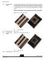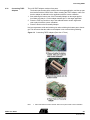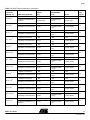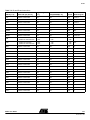
1
ICE50
..............................................................................................
User Guide
Table of Contents
Section 1
Preface ................................................................................................. 1-1
1.1
About this Manual .....................................................................................1-1
1.1.1
Warnings ............................................................................................1-1
1.1.2
Tips.....................................................................................................1-1
1.1.3
Workaround ........................................................................................1-1
1.1.4
Checklists ...........................................................................................1-1
1.1.5
Related Documentation ......................................................................1-2
1.2
ICE50 Firmware History ............................................................................1-2
1.2.1
Version 1.0 .........................................................................................1-2
1.2.2
Version 1.1 .........................................................................................1-2
1.2.3
Version 1.2 .........................................................................................1-2
1.3
ICE50 Known Issues.................................................................................1-2
1.3.1
User Break in Sleep Mode..................................................................1-2
1.3.2
ADC Latch-up .....................................................................................1-2
1.3.3
User Break..........................................................................................1-2
1.4
Reporting Problems ..................................................................................1-3
Section 2
Introduction ........................................................................................... 2-1
2.1
2.2
2.3
ICE50 Contents.........................................................................................2-1
ICE50 Features .........................................................................................2-2
System Requirements...............................................................................2-3
2.3.1
Hardware Requirements.....................................................................2-3
2.3.2
Software Requirements ......................................................................2-3
2.3.3
Target Hardware Requirements .........................................................2-3
2.3.4
Operating Conditions..........................................................................2-3
2.3.5
Host Interface .....................................................................................2-3
Section 3
General Description .............................................................................. 3-1
3.1
General Hardware Description..................................................................3-1
3.1.1
3.2
ICE50 User Guide
What is an In-Circuit Emulator?..........................................................3-1
Main Emulator Unit....................................................................................3-2
3.2.1
Emulator Unit......................................................................................3-2
3.2.2
Status LEDs........................................................................................3-2
i
2523A–AVR–11/02
Table of Contents
3.3
POD Bay ...................................................................................................3-4
3.3.1
Removing POD from POD Bay ..........................................................3-4
3.3.2
Inserting POD Into POD Bay ..............................................................3-4
3.3.3
Expansion Bay....................................................................................3-5
3.3.4
USB Connector...................................................................................3-5
3.3.5
RS-232C Connector ...........................................................................3-5
3.3.6
Reset Button.......................................................................................3-5
3.3.7
Power Switch......................................................................................3-5
3.3.8
Power Connector................................................................................3-6
3.4
Personality Adapter Description................................................................3-6
3.4.1
Personality Adapter Description .........................................................3-6
3.4.2
t26 Personality Adapter ......................................................................3-7
3.4.3
t28 and t29 Personality Adapter .........................................................3-8
3.4.4
m8 Personality Adapter ......................................................................3-8
3.4.5
m32 Personality Adapter ....................................................................3-9
3.4.6
m162 Personality Adapter ..................................................................3-9
3.4.7
m128 Personality Adapter ................................................................3-10
3.4.8
m169 Personality Adapter ................................................................3-10
3.5
POD Description .....................................................................................3-11
3.5.1
POD Description...............................................................................3-11
3.5.2
Digital I/O..........................................................................................3-12
3.5.3
Analog Comparator ..........................................................................3-14
3.5.4
A/D Converter...................................................................................3-14
3.6
Power System Description ......................................................................3-15
3.6.1
Power Supply ...................................................................................3-15
3.6.2
ICE50 Power System .......................................................................3-15
3.6.3
Target Application Power Requirements ..........................................3-16
3.7
Probe Description ...................................................................................3-17
3.7.1
Probe Description .............................................................................3-17
3.7.2
External Clock Signal .......................................................................3-18
3.7.3
Internal Clock Signal Provided by AVR Studio .................................3-18
3.7.4
External 32 kHz RTC Crystal............................................................3-19
3.7.5
Internal RC Oscillator .......................................................................3-19
3.7.6
External Crystal and External Resonator .........................................3-19
3.7.7
External RC Oscillator ......................................................................3-19
3.8
Test Adapter ...........................................................................................3-19
3.8.1
ii
2523A–AVR–11/02
Using the Test Adapter.....................................................................3-20
ICE50 User Guide
Table of Contents
Section 4
Connecting ICE50................................................................................. 4-1
4.1
4.2
4.3
Connecting ICE50 for Emulation...............................................................4-1
Connecting ICE50 to host PC ...................................................................4-1
Connecting the Probe to the Target Board ...............................................4-1
4.3.1
Connecting PDIP Adapters.................................................................4-1
4.3.2
Connecting TQFP Adapters ...............................................................4-3
4.4
ICE50 Power-up Sequence.......................................................................4-4
Section 5
Configuring AVR Studio ........................................................................ 5-1
5.1
5.2
5.3
5.4
5.5
5.6
5.7
5.8
5.9
5.10
ICE50 Emulator Options ...........................................................................5-1
AVR Studio Configuration Quick Start Guide............................................5-2
Device Selection .......................................................................................5-3
Fuses and Lock Bits..................................................................................5-5
Lock Bits ...................................................................................................5-8
ICE Status .................................................................................................5-9
Boot Block Options .................................................................................5-11
Special ....................................................................................................5-12
Downloading New Parts for ICE50..........................................................5-12
Upgrading the ICE50 Firmware...............................................................5-13
Section 6
Special Considerations ......................................................................... 6-1
6.1
Electrical Compatibility ..............................................................................6-1
6.1.1
Power .................................................................................................6-1
6.1.2
I/O Lines .............................................................................................6-1
6.2
6.3
6.4
6.5
Sleep Mode ...............................................................................................6-2
Target Hardware Requirements................................................................6-2
Clock Options............................................................................................6-2
Differences Between Emulator and Part ...................................................6-2
Section 7
Trace..................................................................................................... 7-1
7.1
7.2
7.3
7.4
7.5
7.6
7.7
7.8
ICE50 User Guide
Enabling Trace in AVR Studio...................................................................7-1
The Trace Window ....................................................................................7-2
Contents of Trace Window Based on Instruction (ICE50).........................7-4
Accessing External Data Memory (ICE50 Trace) ...................................7-14
Interrupt Handling (ICE50 Trace) ............................................................7-14
Reset (ICE50 Trace) ...............................................................................7-15
Save Trace Buffer to File (ICE50) ...........................................................7-15
Sleep (ICE50 Trace) ...............................................................................7-15
iii
2523A–AVR–11/02
Table of Contents
Section 8
Troubleshooting .................................................................................... 8-1
8.1
iv
2523A–AVR–11/02
Troubleshooting Guide..............................................................................8-1
ICE50 User Guide
Section 1
Preface
1.1
About this
Manual
This manual is using the nomenclature described in this section to show warnings, tips,
workarounds etc.
1.1.1
Warnings
This manual contains important warnings to prevent damage to your system and the
ICE50. All the warnings are emphasized as shown in the example below.
WARNING!
This is a warning...
Please read all warnings carefully.
1.1.2
Tips
Some sections contain useful tips for using the ICE50. All the tips are emphasized as
shown in the example below.
Tip!
This is a tip...
1.1.3
Workaround
Workaround!
This is a workaround...
1.1.4
Checklists
Once comfortable with the configurtion and use of the ICE50, the checklists at the end of
these sections can be used for fast setup of a new project.
The checklists are of great help for getting the debugging system on-line without problems. However, novice users should also check that the operating conditions of the
target system are compliant to the requirements of ICE50. This is described in the Connecting ICE50 section.
ICE50 User Guide
1-1
Rev. 2523A–AVR–11/02
Preface
1.1.5
Related
Documentation
The following electronic documents from Atmel® are related to the use of the AVR®
microcontrollers, and of the debugging tools. All documents can be found on the Atmel
Products CD-ROM enclosed in the ICE50 kit. For more information and document
updates, please visit our web site: www.atmel.com.
AVR Studio® user's guide.
Describes in detail how to use the AVR Studio debugging environment.
Describes in detail how to use the AVR Assembler.
Data sheets for the different AVR devices.
Errata sheets for the different AVR devices.
Application notes describing different application examples for the AVR
microcontrollers.
Describes in detail how to use the AVR Studio debugging environment.
Note: AVR Studio 4.0 or later is required for ICE50 support. AVR Studio 3.x versions
will not work with ICE50!
1.2
ICE50 Firmware
History
There has been several releases of the ICE50 firmware.
1.2.1
Version 1.0
First released version.
1.2.2
Version 1.1
Errors in trace module fixed.
Version table readout in main module fixed.
1.2.3
Version 1.2
All parts with ADC: ADC bit 3 and 4 where interchanged. This is now fixed on all parts
with ADC.
Trace of Program Counter is now correct in single step.
Brown-out Detection (BOD): Selection of Brown-out Voltage is now enabled for all
parts.
Mega8: Reset Disable Fuse added to ICE50 options.
1.3
ICE50 Known
Issues
There are some known issues in the ICE50 that users needs to be aware of.
1.3.1
User Break in Sleep
Mode
User break in sleep mode is not supported. Use an interrupt to wake up the part or a
reset to Reset the emulator.
User break in sleep mode is not supported. Workaround: A Reset will break and
reset the emulator.
1.3.2
ADC Latch-up
The ADC may latch-up if the target is powered before the ICE. Also make sure that
no residual voltage is present on the ADC input pins if the ICE is not powered.
1.3.3
User Break
User break in sleep mode is not supported. Use an interrupt to wake up the part or a
reset to reset the emulator.
1-2
2523A–AVR–11/02
ICE50 User Guide
Preface
1.4
Reporting
Problems
ICE50 User Guide
Problems with AVR Studio can be reported to [email protected]. Problems with beta
releases can be reported to [email protected].
1-3
2523A–AVR–11/02
Preface
1-4
2523A–AVR–11/02
ICE50 User Guide
Section 2
Introduction
ATICE50 is an advanced In-Circuit Emulator that covers a wide range of the eight bits
AVR microcontrollers from Atmel. This section gives a brief introduction to it’s features.
2.1
ICE50 Contents
Figure 2-1.
The ATICE50 contains the following items:
ICE50 Main Unit/Pod/Two FPC (Flexible Printed Circuit) Cables & Probe
Personality Adapters for:
– ATmega8
– ATmega16
– ATmega162
– ATmega32
– ATmega128
– ATtiny26
ICE50 User Guide
2-1
Rev. 2523A–AVR–11/02
Introduction
9-pin RS-232C Cable
USB Cable
Power Supply
European Power Supply Cable
US Power Supply Cable
AVR Technical Library CD-ROM
– AVR Data Sheets
– Application Notes
– AVR Studio 4.00 or Later
ICE50 Quick Start Guide
2.2
ICE50 Features
The ICE50 In-circuit Emulator is a High-end Emulator from Atmel designed to emulate a
wide range of AVR devices. The ICE50 is controlled by AVR Studio 4.0 or later. Present,
the following devices are supported:
– ATtiny26
– ATmega8
– ATmega16
– ATmega162
– ATmega32
– ATmega128
– ATmega169
– ATmega8515
– ATmega8535
The ICE50 supports the following features:
Emulates All Digital and Analog Peripherals
Target Voltage Range 2.2V - 5.5V
Full Target Frequency Range for All Supported Devices
Watches
Trace Buffer
Unlimited Number of Break Points
Symbolic Debugging Support
Full Visibility of and Access to Register File, SP, PC, and Memories
Access to all I/O Registers
I/O Configurable to Run or Halt in Stopped Mode
Cycle Counter
2-2
2523A–AVR–11/02
ICE50 User Guide
Introduction
2.3
System
Requirements
The following minimum requirements apply for the ICE50.
2.3.1
Hardware
Requirements
For using the ICE50 with AVR Studio, a Pentium 233 MHz (or more) class personal
computer with following specifications is recommended:
64 MByte RAM, or more
20 MByte of free hard disk (HD) space
CD-ROM or Internet access
Recommended Screen Resolution 1024x768
16650 Compatible Serial Port (COM port)
AVR Studio v4.0 or later installed
Acrobat Reader v4.0 or later installed (optional).
2.3.2
Software
Requirements
The following operating systems are currently supported by AVR Studio:
Windows NT® Version 3.51(1)
Windows NT Version 4.0(1)
Windows® 95
Windows 98 (ME)
Windows 2000
Windows XP
AVR Studio is always updated to fit new operating systems and versions. See AVR
Studio User's Guide for latest information.
Note:
1. Windows NT 3.51 and Windows NT 4.0 does not support USB communication.
2.3.3
Target Hardware
Requirements
The target must be able to supply 2.2 - 5.5V @150mA. See Table 3-6 for further
information.
2.3.4
Operating
Conditions
Operation Temperature: 0°C - 70°C
Operating Humidity: 10 - 90 % RH (non-condensing)
Supply Voltage: +9.0V to +12.0V DC
WARNING!
Violating the recommended operating conditions for the ICE50 might cause incorrect operation and damage the emulator.
2.3.5
Host Interface
ICE50 User Guide
RS-232C @ 115200 bps, 1 start-, 8 data-, and 1 stop-bit, no parity with hardware handshaking. 9-pin female connector with RTS and CTS connected to support hardware
handshaking.
2-3
2523A–AVR–11/02
Introduction
2-4
2523A–AVR–11/02
ICE50 User Guide
Section 3
General Description
This setion describes the different components of the ATICE50 in detail.
3.1
General
Hardware
Description
In this section a brief description of emulation is given, and a closer look at the parts that
make up the ICE50.
3.1.1
What is an In-Circuit
Emulator?
The ICE50 is an In-Circuit Emulator. An emulator is a dedicated piece of hardware
designed to “emulate” the behaviour of another piece of hardware. In the case of the
ICE50, it is designed to behave as a wide range of AVR devices. Exact emulation is the
goal for all emulators and the ICE50 offers the highest possible level of compatibility.
The ICE50 emulator system consists of the following five modules:
Main Emulator Unit
POD
Probe
Personality adapters
Test adapter
ICE50 User Guide
3-1
Rev. 2523A–AVR–11/02
General Description
3.2
Main Emulator
Unit
The main emulator unit contains the “brain” of the ICE50.
3.2.1
Emulator Unit
The main emulator unit is shown in Figure 3-1. The main unit contains the control logic,
and general hardware necessary to emulate an AVR device.
Figure 3-1. ICE50 Main Emulator
Reset
Button
RS-232C/
USB
Power Connector/
Power Switch
POD Bay
Expansion Bay
LEDs
Status LEDs
POD Bay
Expansion Bay
USB Connector
RS-232C Connector
Reset Button
Power Switch
Power Connector
3.2.2
Status LEDs
There are three LEDs on the front of the ICE50 cabinet. One red, one red/green duo
LED and one green LED. All these LEDs give important status information on the ICE50
and which mode it is operating in. The picture below shows a close-up of the LEDs.
When turning on power on the ICE50 the normal LED sequence will be as follows:
1. Red Power LED turns ON.
2. Mode LED turns ON and is first red and next orange.
3. Green status LED turns ON (after approx 15 seconds).
This indicate that the unit is operating and ready for use.
Figure 3-2. Emulator LEDs
3-2
2523A–AVR–11/02
ICE50 User Guide
General Description
3.2.2.1
Red Power LED
The red LED is the power indicator LED. This will be lit if power on the ICE50 is turned
on and the power system is working correctly. If the LED stays off after power on, make
sure the power supply meets the requirements of the ICE50. If using another power supply than the one supplied with the ICE50 make sure that the power polarity is correct.
See the Power System section for more details on power requirements.
3.2.2.2
Multi Color Mode
LED
The Multicolor LED displays information about which mode the ICE50 is working in. During the startup sequence this LED is first red, next orange. Orange indicates that the
Emulator is in stopped mode. A green light indicates that the ICE is in run mode. If the
LED turns red it indicates an emulator error. If this happens consult the troubleshooting
guide.
3.2.2.3
Green Status LED
The green LED will be turned on when the ICE50 is ready for emulation. Once the green
LED is on, the ICE50 is ready for emulation. The LED will flash during upgrading of the
ICE50. The LED will be turned off during loading of a new part, and lit when the part is
finished loading. If the LED does not turn on after a power up sequence please consult
the troubleshooting guide for possible solutions.
Figure 3-3. Multi Color Mode
Table 3-1. LED Color Definitions
LED
Meaning
Red
Power
Multi
Green
ICE50 User Guide
Mode
Status
State
Description
Off
Power not connected, or ICE50 Turned off.
On
Power connected, ICE50 on and voltages OK.
Green
Run mode
Red
Error condition, if permanently lit.
Orange
Stopped mode
Off
ICE50 is initializing.
On
ICE50 Ready for emulation.
Blinking
The LED will flash when doing an upgrade.
3-3
2523A–AVR–11/02
General Description
3.3
POD Bay
The ICE50 has a very flexible architecture that will ensure a long product life. The different AVR devices are characterised through their number of I/O pins and analog
features. Both the I/O pins and the analog features are implemented on the POD board.
If new AVR devices are made available to the market that contain I/O or analog features
that cannot be emulated by the current POD, Atmel is dedicated to create new POD
modules that support the functionality of the new devices.
3.3.1
Removing POD from
POD Bay
If for some reason the POD must be removed from the POD Bay, the recommended
procedure is as described below. See also Figure 3-4.
1. Lift the POD on the front edge until a click is heard. The POD is now ready to be
pulled up from the bay.
2. Lift the POD out of the Bay.
Figure 3-4. Removing POD from POD Bay
Without the POD connected, the ICE50 will still be able to emulate core functions of the
AVR (e.g., timers). This feature can be useful in some debugging sessions. If the POD is
inserted and there is no target power applied, the ICE will be held in Reset until target
power is turned on. By disabling POR and BOD Reset in ICE50 other options dialog,
ICE50 will emulate correctly even if target power is not connected.
3.3.2
Inserting POD Into
POD Bay
Only original ICE50 Pods should be used with ICE50 and care should be taken when
placing or removing the POD. During normal use there is no need to remove the POD
from the bay. If for some reason the POD is disconnected, the recommended procedure
to re-insert the POD is as follows. See also Figure 3-5.
1. Place the POD in the ICE50 POD connector. Make sure that the connector male
and female guides align.
2. Use both hands and apply pressure on the upper half of the POD (on top of the
connector).
3. After pressing the connector firmly in place, use one hand to apply pressure on
the lower half of the POD. You will hear a click when the POD locks into position.
3-4
2523A–AVR–11/02
ICE50 User Guide
General Description
Figure 3-5. Inserting POD Into POD Bay
3.3.3
Expansion Bay
The expansion connector is intended for future use, and not used in the current version
of ICE50. The POD placed in this socket is an empty POD enclosure and serves the
purpose of protecting the Expansion Connector.
3.3.4
USB Connector
USB communication is supported in AVR Studio 4, Build 181 and higher versions. USB
Drivers are found on the AVR Technical Library CD-Rom. The USB port is shown in Figure 3-6
Figure 3-6. USB-, RS-232C-communication, and Reset Button
3.3.5
RS-232C Connector
Present, all communication between the ICE50 and AVR Studio is done through a standard RS-232C interface. This is the communication protocol used by COM ports on
PCs. The communication runs at 115200 bit/s, no parity, 8 data bits, 1 stop bit, (N81).
For information on how to connect the ICE50 to a PC see the Connecting ICE50 to PC
section. See Figure 3-6.
3.3.6
Reset Button
By pressing the reset button on the ICE50, a Warm Reset of the Emulator is preformed.
After approximately 15 seconds the configuration is completed, and the green status
LED will turn on indicating that the emulator is ready for use. See Figure 3-6.
3.3.7
Power Switch
The Power Switch is the main on/off switch for the ICE50 Emulator. Switching this off
will turn off power on the ICE50. The ICE50 will however remain grounded to the power
supply. See Figure 3-7.
ICE50 User Guide
3-5
2523A–AVR–11/02
General Description
Figure 3-7. Power Switch and Connector
3.3.8
Power Connector
The Power Connector on the ICE50 system is a standard type with 2.1 mm center tap.
Ground should be connected to the center tap. For more information about power
requirements and operating conditions see the Power System Description. See Figure
3-7.
3.4
Personality
Adapter
Description
The personality adapters of the ICE50 provides the physical adaption between the
ICE50 and the target device.
3.4.1
Personality Adapter
Description
ICE50 is supplied with a range of personality adapters. These adapters map the pinout
from the ICE50 POD to each of the microcontrollers it supports. Each adapter includes
an identification code that the ICE50 and AVR Studio use for automatic device detection. The ICE50 package contains the following Personality Adapters:
Each adapter corresponds to one pinout type and supports one or more AVR microcontrollers. Table 3-2 shows which devices are supported by the different Personality
Adapters.
Table 3-2. Personality Adapters
3-6
2523A–AVR–11/02
Device
Use Personality Adapter Named
Seral Number
ATmega16
m32
A9902.3.1310.A
ATmega128
m128
W10635SDF
ATmega32
m32
A9902.3.1310.B
ATtiny28/29
t28/t29
A9902.3.1350.B
ATtiny26
t26
A9902.3.1370.A
ATmega162
m162
A9902.3.1300.B
ATmega8
m8
A9902.3.1390.C
ATmega169
m169
W10634SDF
ICE50 User Guide
General Description
3.4.1.1
Connecting the
Personality Adapter
to the Probe
When connecting the Personality Adapter and the Probe, make sure that the Probe is
connected with the correct orientation. The connectors will only fit when the boards have
the correct orientation. On the Personality Adapters a circle indicates pin 1. Make sure
that the circle on the Probe matches the circle on the Personality Adapter as shown in
Figure 3-8.
Figure 3-8. Connecting Personality Adapter to Probe
3.4.2
t26 Personality
Adapter
The t26 Personality adapter is a PDIP adapter for t26 devices. The footprint is a standard 20-lead 0.300" wide, PDIP package. If the target uses another package type, an
additional adapter has to be purchased from a third party vendor. When connecting the
Personality Adapter to the Probe, make sure to align the circles on the Probe and Personality Adapter as shown above.
Figure 3-9. t26 Personality Adapter(1)
Note:
3.4.2.1
Supported Devices
ICE50 User Guide
1. SNR: A9902.3.1370.A
ATtiny26
3-7
2523A–AVR–11/02
General Description
3.4.3
t28 and t29
Personality Adapter
The t28 Personality adapter is a PDIP adapter for t28 devices. The footprint is a standard 28-lead 0.300" wide, PDIP package. If the target uses another package type, an
additional adapter has to be purchased from a third party vendor. When connecting the
Personality Adapter to the Probe, make sure to align the circles on the Probe and Personality Adapter as shown above.
Figure 3-10. t28 and t29 Personality Adapter(1)
Note:
1. SNR: A9902.3.1350.B
3.4.3.1
Supported Devices
ATtiny28
3.4.4
m8 Personality
Adapter
The m8 Personality adapter is a PDIP adapter for m8 devices. The footprint is a standard 28-lead 0.300" wide, PDIP package. If the target uses another package type, an
additional adapter has to be purchased from a third party vendor. When connecting the
Personality Adapter to the Probe, make sure to align the circles on the Probe and Personality Adapter as shown above.
Figure 3-11. m8 Personality Adapter(1)
Note:
3.4.4.1
Supported Devices
3-8
2523A–AVR–11/02
1. SNR: A9902.3.1390.C
ATmega8
ICE50 User Guide
General Description
3.4.5
m32 Personality
Adapter
The m32 Personality adapter is a PDIP adapter for m32/m16 devices. The footprint is a
standard 40-lead 0.600" wide, PDIP package. If the target uses another package type,
an additional adapter has to be purchased from a third party vendor. When connecting
the Personality Adapter to the Probe, make sure to align the circles on the Probe and
Personality Adapter as shown above.
Figure 3-12. m32 Personality Adapter(1)
Note:
1. SNR: A9902.3.1310.B
3.4.5.1
Supported Devices
ATmega32/ATmega16
3.4.6
m162 Personality
Adapter
The m162 Personality adapter is a PDIP adapter for m162 devices. The footprint is a
standard 40-lead 0.600" wide, PDIP package. If the target uses another package type,
an additional adapter has to be purchased from a third party vendor. When connecting
the Personality Adapter to the Probe, make sure to align the circles on the Probe and
Personality Adapter as shown above.
Figure 3-13. m162 Personality Adapter(1)
Note:
3.4.6.1
Supported Devices
ICE50 User Guide
1. SNR: A9902.3.1300.B
ATmega162
3-9
2523A–AVR–11/02
General Description
3.4.7
m128 Personality
Adapter
The m128 Personality Adapter is a TQFP64 adapter, and it consists of two modules.
The bottom module has the TQFP footprint, and should be soldered on the target application. Make sure to solder it with the correct orientation. Pin 1 is indicated with a printed
“1” as shown here. Once the bottom module is soldered into the application, connect the
top module. Make sure that pin 1 on the top module matches the pin 1 on the bottom
module.
Once the Personality Adapter is securely mounted, place the Probe on the Personality
adapter. The circle marked on the Probe should align with pin 1 on the m128 adapter.
Figure 3-14. m128 Personality Adapter(1)
Note:
1. SNR: W10635SDF
3.4.7.1
Supported Devices
ATmega128
3.4.8
m169 Personality
Adapter
Figure 3-15. m169 Personality AdapterFigure 1
Note:
3.4.8.1
Supported Devices
3-10
2523A–AVR–11/02
1. SNR: W10634SDF
ATmega169
ICE50 User Guide
General Description
3.5
POD Description
The ICE50 POD implements all digital I/O and analog functionality of the current AVR
family of devices. If new AVR devices are made available to the market that contain I/O
or analog features that cannot be emulated by the current POD, Atmel is dedicated to
create new POD modules that support the functionality of the new devices.
3.5.1
POD Description
The ICE50 POD is shown in Figure 3-16. It connects to the main unit through two docking connectors. When connecting or disconnecting the POD do not use excessive force
as this might damage the POD.
Figure 3-16. ICE50 POD
The POD contains all analog and digital logic necessary to emulate the target AVR
device. The circuitry is designed to give as close as possible electrical characteristics as
the real device. The POD emulates the following functions:
Digital I/O
Analog Comparator
A/D Converter
The ICE50 is a jumperless design. All configuration of the POD is done through AVR
Studio. No manual configuration of jumpers is necessary.
ICE50 User Guide
3-11
2523A–AVR–11/02
General Description
3.5.2
Digital I/O
The Digital IO ports of the ICE50 are realized as shown in Figure 3-17 using CMOS buffers and voltage converters.
Figure 3-17. Digital I/O
DIGITAL I/O
LEVEL CONVERTER
VCC Emulator
VCC Target
PULLUP (DDRxy & PORTxy)
VCC
DDRxy
36K
PORTxy
Pxy
PINxy
PINKEEPx
330K
The propagation delay of the IO ports are larger for the ICE50 than for the actual emulated part. The diagram below shows the timing data for driving out and reading in a
signal on the IO ports of the Emulator. The data direction register is assumed set to “1”
in Figure 3-18. Table 3-3 shows typical data.
Figure 3-18. Data Direction Register
PORTxy
tOLH
tOHL
Pxy
PINxy
tIHL
3-12
2523A–AVR–11/02
tILH
ICE50 User Guide
General Description
Table 3-3. Data Direction
Delay
Typical Value (2V Target)
Typical Value (5V Target)
tOHL
(1)
13 ns
10 ns
tOLH
(2)
13 ns
10 ns
(3)
13 ns
10 ns
tILH(4)
13 ns
10 ns
tIHL
Notes:
1.
2.
3.
4.
tOHL = Time from clearing the PORT register to the output changes
tOLH = Time from setting the PORT register to the output changes
tIHL = Time from changing the input level to the PIN signal changes (high to low)
tILH = Time from changing the input level to the PIN signal changes (low to high)
Figure 3-19 shows the timing data for tristating/driving the IO pins. Table 3-4 shows
related typical data.
Figure 3-19. Timing Data
DDRxy
tDLZ
tDZL
PORTxy
tDZH
tDHZ
Pxy
High Z
High Z
High Z
Table 3-4. Timing Data
Delay
Typical Value (2V target)
Typical Value (5V target)
(1)
15 ns
15 ns
tDLZ(2)
15 ns
15 ns
tDZH
(3)
15 ns
15 ns
tDHZ
(4)
15 ns
15 ns
tDZL
Notes:
1.
2.
3.
4.
tDZL = time from setting the DDR register to the output is driven low.
tDLZ = time from clearing the DDR register to the output is tristated.
tDZH = time from setting the DDR register to the output is driven high.
tDHZ = time from clearing the DDR register to the output is driven low.
The drive capability of the output buffers are ± 24 mA at 3V VCC. This slightly exceeds
the driving capability of the actual parts. The operating voltage range of the IO circuits
are 2 VCC to 5.5 VCC. At 2V VCC the buffers are able to sink 25 mA with a maximal output
low voltage (VOLmax) of 1V.
The hysteresis voltage for the input buffers are typically 0.8V at 3V VCC and 1.2V at 5.5V
VCC.
ICE50 User Guide
3-13
2523A–AVR–11/02
General Description
3.5.3
Analog Comparator
The Analog Comparator is built around a high speed comparator and a CMOS output
buffer/voltage converter. Figure 3-20 shows the Analog Comparator block diagram. The
total propagation delay from the AIN0 and AIN1 pins to the internal ACO signal is typically 90ns, max 210ns. For parts, the total propagation delay from the AIN0 and AIN1
pins to the internal ACO signal is typically 500 ns, max 750 ns.
The comparator features an internal hysteresis of typical 1 mV, max 4 mV @ 25°C to
ensure clean switching.
Figure 3-20. Analog Comparator Block Diagram
ANALOG COMPARATOR
1.2V
ACBG
ACD
AIN0
+
ACO
100R
AIN1
ACME
ADEN
ADC Multiplexer
Output
3.5.4
A/D Converter
The block diagram of the ICE50 AD converter is shown in Figure 3-21.
Figure 3-21. ICE50 AD Converter
A/D Converter
ADC7
ADC6
ADC5
ADC4
ADC3
ADC2
ADC1
ADC0
330Ω
VCC
330Ω
330Ω
330Ω
330Ω
Pos
Input
Mux
ADC Multiplexer Output
10-bit ADC
330Ω
Vin
1.2V
330Ω
Q[0..9]
330Ω
Vref
1x/10x/100x
+
VCC
-
10K
1x/2x
+
ref
10K
-
ref
Neg
Input
Mux
ADMUX Decoder
+
-
AVCC
Aref
10K
+
10K
-
Vref
2
330Ω
330Ω
2.5V
Voltage
Aref Out Reference
Selection
3-14
2523A–AVR–11/02
ICE50 User Guide
General Description
The ADC is built using analog multiplexers, programmable gain instrumentation amplifiers and a 10-bit successive approximation A/D converter. This construction should have
the same performance as the actual part, but since the ADC is located on the POD as
an external construction the analog components will be more susceptible to ambient
noise and noise from switching IO lines.
Note: Internal analog reference voltage is set to 2.5 volt when using the emulator. This
differs from part which uses 2.56 V. Due to this fact ADC conversions done by
the emulator using the internal analog reference voltage differ from the conversions done in part.
All inputs to the ADC have serial current limiting resistors of 330Ω. This is to protect the
inputs of the ADC circuit when the emulator is switched off and the target power is
present. The outputs of the input multiplexers are clamped to VCC and GND and thus
when target VCC is present and the emulator power is turned off there will flow a current
of approximately (Vinput - 0.3V)/330Ω through each ADC input pin.
3.6
Power System
Description
The ICE50 needs external power in order to function. A switching power adapter is supplied with the unit. The power adapter will accept input voltages in the range of 100VAC
to 240VAC and frequencies from 50Hz to 60Hz. This will cover most situations.
3.6.1
Power Supply
Figure 3-22. Power Supply
The power supply delivered with ICE50 is dimensioned to meet the requirements of the
Emulator. If another power supply is used, it should supply a voltage between 9 and 15
VDC, and a minimum of 20W. It connects to the main unit through a standard connector
with 2.1 mm center tap. Ground is connected to the center tap.
3.6.2
ICE50 Power System The ICE50 has an internal power regulator designed to deliver regulated voltages for
use by the ICE itself. The power system is not designed to provide external power to the
target application.
ICE50 User Guide
3-15
2523A–AVR–11/02
General Description
3.6.3
Target Application
Power
Requirements
The Probe and parts of the POD are powered by the target application power system.
The dynamic power requirements of the Probe/POD will not differ significantly from the
power requirements of the actual device. See below for power requirements. The static
power requirement for the POD is listed in Table 3-6. The target power system must be
dimensioned to tolerate this current consumption.
Table 3-5. Power Requirements
Power Requirements
9 - 15 VDC
Power Voltage Requirements
< 20 W
Power Consumption
2.7 - 5.5 V
Target Application Voltage Range
Table 3-6. Target Voltage
ICE50 (POD/Probe) current consumption from Target Application,
Target Voltage
Normal (Typical)
Worst Case
2.5V
5 mA
7 mA
3.3V
20 mA
30 mA
5.0V
85 mA
125 mA
5.5V
110 mA
165 mA
Note:
3-16
2523A–AVR–11/02
The Digital I/O drive capabilities of the ICE50 POD differ slightly from what can
be expected in the actual device. For details on the Digital I/O drive capabilities
compared to the actual device, please see the Digital I/O section of the POD
description.
ICE50 User Guide
General Description
3.7
Probe
Description
The ICE50 probe is the link between the flex cable going out from the POD and the Personaliy Adapter that fits into the target application. The main purpose of the probe is to
route all the signals from the flex cable to the appropriate pins of the personality adapter.
In addition the Probe implements current limitation on all the I/O pins in order to protect
both the target and the POD. The probe also implements proper line termination in order
to avoid ringing on high freuency signals.
3.7.1
Probe Description
The Probe contains clock driver circuitry for the ICE50, voltage polarity and short circuit
protection. Figure 3-23 show a picture of the probe and a simplified block diagram of
how the clock driver circuitry is implemented is shown in Figure 3-24 and Figure 3-25.
By putting the clock driver circuitry on the Probe (as close as possible to the target
board) the best possible emulation of the AVR clock options are achieved.
Figure 3-23. Probe
Figure 3-24. Timer Oscillator
Enable
Output
ICE50 User Guide
Timer
Oscillator
Drive
3-17
2523A–AVR–11/02
General Description
Figure 3-25. External Clock
Enable
XTAL1
Enable
XTAL2
3.7.1.1
Available Clock
Options
The current version of the Probe has some restrictions with regards to clock options
support. The unsupported clock modes are quite easy to emulate with simple
workarounds as described in Section 3.7.6 and Section 3.7.7. The Probe version can be
found on top of the back side of the Probe (left side of the right picture above).
3.7.1.2
ICE50 Probe version
A9902.3.1200.E
Version A9902.3.1200.E of the Probe supports the following clock options:
External Clock Signal
Internal Clock Signal provided by AVR Studio
External 32 kHz RTC Crystal
Internal Calibrated RC Oscillator
The following clock options are not supported by Probe version A9902.3.1200.C. A
description for workarounds for the unsupported clock modes can be found in section
“External Crystal and External Resonator” on page 19 and “External RC Oscillator” on
page 19.
3.7.2
External Clock
Signal
An external clock signal can be applied to the XTAL1 pin on the emulator probe. The
Emulator can then be set up to use this signal as the system clock. See device selection
for a description of how to set up AVR Studio for this option. The clock signal must meet
the conditions as shown in Table 3-7.
Table 3-7. Clock Signal Conditions
Value
3.7.3
Internal Clock Signal
Provided by AVR
Studio
3-18
2523A–AVR–11/02
Frequency
5KHz to 20MHz
Duty cycle
50%
Absolute maximum input voltage
1.8 - 7.0V
Recommended input voltage
1.8 - 5.5V
Minimum high level input voltage
1.7V
Maximum low level input voltage
0.5V
The Emulator may be set up to run on an internal programmable clock. The frequency
range of this programmable clock is 5 kHz to 20 MHz. However, the maximum frequency cannot be set higher than the speed limit of the actual part. Only certain output
frequencies are possible to generate with highest accuracy. However the clock generator generally produces an output frequency within 0.1% of the desired output frequency.
If the target application should run on the same clock as the AVR chip/emulator, the
internal programmable clock may be driven out on the XTAL2 pin. See section device
selection for a description of how to set up the internal programmable clock.
ICE50 User Guide
General Description
3.7.4
External 32 kHz RTC
Crystal
The Asynchronous Timers in the emulated part may be clocked by an external 32 kHz
crystal. This crystal should be connected to the TOSC1 and TOSC2 pins of the personality adapter. To ensure proper operation the crystal should be connected as close to
the personality adapter as possible. The Oscillator driver on the probe is designed to
work with most parallel mode 32 kHz crystals.
3.7.5
Internal RC
Oscillator
In AVR Studio the Emulator may be set to run on an Internal RC Oscillator. See section
device selection for a description of how to set up the Internal RC Oscillator.
3.7.6
External Crystal and
External Resonator
External crystal/resonator is not supported on the ICE50 probe. Instead, configure the
Emulator to use the internal programmable clock. The XTAL1 pin will then be tri-stated.
XTAL2 pin will be enabled and the internal programmable clock is driven out on the
XTAL2 pin. See special section for a description of how to set up the XTAL2 clock.
3.7.7
External RC
Oscillator
External RC Oscillator is not supported on the ICE50 probe. Instead, configure the emulator to use the internal programmable clock. The XTAL1 and XTAL2 pins will then be
tristated.
3.8
Test Adapter
ICE50 is supplied with a Test Adapter. See Figure 3-26.
Figure 3-26. Test Adapter(1)
Note:
1. SNR: A9902.3.1400.A
The adapter includes an identification code that the ICE50 and AVR Studio uses for
detection. The ICE50 Test Adapter is used for the following tests:
Analog Comparator
Analog Digital Converter
I/O pins
ICE50 User Guide
3-19
2523A–AVR–11/02
General Description
3.8.1
Using the Test
Adapter
The test adapter must be connected to the probe.
To start the test program open AVR Studio and select from the drop down menu: Tools>ICE50 Selftest. The window showing in Figure 3-27 will appear:
Figure 3-27. Start Test Program in AVR Studio
The tests that require a Test Adapter connected to the probe are the ones marked on
the list above. Select the test that should be run, and press the “Run” button to start the
test. Finally, the test program will show the status of the test.
Note: AVR Studio 4.0 or later is required for ICE50 support. AVR Studio 3.x versions
will not work with ICE50!
Tip!
AVR Studio is constantly being updated. Check for upgrades at www.atmel.com.
3-20
2523A–AVR–11/02
ICE50 User Guide
Section 4
Connecting ICE50
ICE50 connects to both the PC where the firmware development is being made and the
target application. This section describes the connection procedure.
4.1
Connecting
ICE50 for
Emulation
This section will describe how to connect and configure the ICE50 for correct operation.
This task can be divided in the following tasks:
1. Selecting correct Personality Adapter
2. Connecting the Probe to the Target Board
3. Connecting ICE50 to PC
4. Correct Power-Up Sequence
5. Configuring AVR Studio
Please follow the above description to make sure that the ICE50 is configured properly!
4.2
Connecting
The ICE50 connects to the host PC through a standard COM port. Make sure that the
ICE50 to host PC ICE50 is powered down before connecting the cable between the ICE50 and the host
PC. Use the 9-pin RS-232C cable that is shipped with the ICE50. Connect the male
cable connector to the ICE50 and the female connector to the host PC. The communication runs at 115200 bit/s, no parity, 8 data bits, 1 stop bit, (N81), and with hardware
handshake.
AVR Studio can not force control over a COM port. If other equipment or software drivers have control of the COM port (eg. IrDA, PDA, Scanner.. ) communication with the
ICE50 will fail. Make sure that no other software has control of the COM port that ICE50
is connected to.
Note: The USB interface is not supported in the current version of the ICE50. Once
the ICE50 is connected to the host PC, continue with connecting the probe to
the target board.
4.3
Connecting the
Probe to the
Target Board
The Probe is connected to the target board through one of the supplied Personality
Adapters. To ensure correct operation make sure that the correct Personality Adapter is
used.
4.3.1
Connecting PDIP
Adapters
Before connecting the ICE50 to the target application, make sure that the ICE50 and the
target application are not powered. This also applies when removing the ICE50. When
ICE50 User Guide
4-1
Rev. 2523A–AVR–11/02
Connecting ICE50
connecting or disconnecting the ICE50 from the host PC, make sure that the ICE50 is
not powered.
1. Inserting the personality adapter. Make sure that pin 1 on the personality adapter
corresponds with pin 1 on the target socket/footprint.
2. Mount the Probe onto the personality adapter. Do not use excessive force; the
Probe only fits one way into the personality adapter. Use the circles on the Personality Adapters and the Probe to safely determine correct orientation. Make
sure that the probe is connected to the pod connector on the ICE50.
Figure 4-1. Connecting PDIP Adapters (Part One of Two)
Note:
1. Place the Personality Adapter in the target application socket. Make sure that the dot
on the Personality Adapter match pin 1 in the target socket.
Figure 4-2. Connecting PDIP Adapters (Part Two of Two)
Note:
4-2
2523A–AVR–11/02
1. Place the Probe on the Personality Adapter. The circle on the probe should face in
the same direction as the dot on the Personality Adapter.
ICE50 User Guide
Connecting ICE50
4.3.2
Connecting TQFP
Adapters
The m128 TQFP adapter consists of two parts:
The bottom part that should be soldered into the target application, and the top part
that interface with the ICE50 Probe. When mounting the TQFP adapter, make sure
that the adapter is soldered into the application with the correct orientation.
1. Start soldering the bottom part of the Personality Adapter on the target application. Make sure that pin 1 on the adapter matches pin 1 in the target application.
2. Place the TQFP top module on top of the soldered bottom module. Again take
care to place it with the correct orientation.
3. Place the Probe on the Personality Adapter.
Use low temperature solder and soldering iron when soldering the bottom part to the target. This will ensure that the solder on the adapter is not removed during soldering.
Figure 4-3. Connecting TQFP Adapters (Part One of Three)
Note:
ICE50 User Guide
1. Place and solder the bottom module. Take care to place it with correct orientation.
4-3
2523A–AVR–11/02
Connecting ICE50
Warning!
Every design precaution is taken so that the probe and ICE50 POD should not be
damaged if incorrectly placed. However, selecting wrong adapter, or placing the
adapter with wrong orientation may damage the ICE50 POD.
Connecting or disconnecting the POD or Personality Adapter while the target application
is powered might damage the Probe and/or the POD.
Once the Probe and Personality Adapter are connected, continue by correct Power-up
sequence.
4.4
ICE50 Power-up
Sequence
When the ICE50 is properly connected to the target and the host PC, the power can be
turned on. The following procedure is recommended to ensure proper communication
between the ICE50 and AVR Studio.
Power up ICE50, wait for yellow LED to be lit.
Power up target board.
Start AVR Studio.
Note: The equipment will not be harmed in any way if a different power up sequence
is used, but since AVR Studio tries to detect peripherals when started, the
ICE50 will not be detected if not powered.
Once the power-up sequence is done, the next step is to start up and configure AVR
Studio. For more information on Power Supply requirements follow this link.
4-4
2523A–AVR–11/02
ICE50 User Guide
Section 5
Configuring AVR Studio
When the ICE50 is properly connected to the target application, the next step is to set
up the correct device configuration in AVR Studio. This is required when an application
project is opened for the first time, and can later be changed in the emulator options
menu. The configuration is stored in a separate file, and will automatically be loaded
when starting the project later.
This section is divided in two subsections:
1. One Quick Start Guide describing the procedure to get the AVR Studio
configured.
2. One subsection describing all emulator options in detail.
5.1
ICE50 Emulator
Options
Device Selection Options
Fuses
ICE Module/Revision list
Special
Note: AVR Studio 4.0 or later is required for ICE50 support. AVR Studio 3.x versions
will not work with ICE50!
ICE50 User Guide
5-1
Rev. 2523A–AVR–11/02
Configuring AVR Studio
5.2
AVR Studio
Configuration
Quick Start
Guide
Follow the procedure described below to configure the ICE50:
1. Connect the ICE50 and start AVR Studio. See Connecting ICE50 for a more
detailed description.
2. Select between creating a new or opening an existing AVR Assembler project.
See picture below.
3. If you have already made an object file you can open this directly. See Figure 51.
Figure 5-1. Welcome to AVR Studio 4
4. If a new project is chosen, type in the project name. Check create initialfile if you
would like an assembler file with the same name as the project. If you would like
a folder created with the same name check this option. Browse to select location
for the project. See Figure 5-2.
Figure 5-2. New Project Window
5-2
2523A–AVR–11/02
ICE50 User Guide
Configuring AVR Studio
5. Press the next button. Now select ICE50 as target and then chose the part to
emulate. Press finish to complete the wizard. AVR Studio will now be ready for
use. See Figure 5-3. Parts that are downloaded and available in ICE50 are
shown highlighted. If a part in grey colour is selected the tool for downloading
new parts is launched. See download new parts for ICE50.
Figure 5-3. AVR Studio 4 Screenshot
5.3
Device Selection
1. In AVR Studio go to Debug->ICE50 Options. Device Selection is highlighted and
it is possible to choose from different parts in the pulldown menu. Note the icon
to the left for each part name. Click this icon if this part is to be loaded into the
ICE50. A total of four part files can be contained in the ICE50 at the same time.
Some part files contain two AVR emulator parts. The status bar at the right side
indicates how many part files ICE50 contains.
For ATmega128 it is also possible to choose ATmega103 compatibility mode.
2. Select between the following clock sources:(This will affect the fuse settings for
the actual part).
– Internal XTAL Oscillator
– Internal RC Oscillator
– External Clock
3. Different start-up times can be selected from the Start-up time pulldown menu.
(This will affect the fuse settings for the actual part.)
4. Part frequency can be selected from the frequency pulldown menu as shown in
Figure 5-4 or the frequency can be typed in the editor box.
ICE50 User Guide
5-3
2523A–AVR–11/02
Configuring AVR Studio
Figure 5-4. Device Selection
In addition two buttons called ICE Reset and Set Default are located in the lower left corner. See Figure 5-4. The ICE Reset button resets the ICE while the set Default button
loads the default settings. ICE reset performs the same reset as the reset button on the
back of the ICE50.
5-4
2523A–AVR–11/02
ICE50 User Guide
Configuring AVR Studio
5.4
Fuses and Lock
Bits
The Fuse- and Lock bit settings in the part can be viewed and configured from AVR Studio. The Fuse settings can only be viewed and not edited in the “Fuse and Lock bit”
view. Configuration is performed in the other views.
In AVR Studio go to Debug->ICE50 options. Highlight Fuses and Lock bits. It is now
possible to view 4 different settings. Note that Fuses marked with “!” do not affect
emulation.
Figure 5-5. Fuse and Lock Bits Settings
1. By pressing “Extended” Fuse the tree expands and it is possible to see the settings for this fuse. “0” indicates on or Fuse programmed, “1” indicates off. It is not
possible to edit the Fuse setting here. The Extended Fuses are available for
selected parts. See the datasheet for the part when configuring the Fuses. In this
case the ATmega128. The Extended Fuse is used to support special features.
See Figure 5-6.
ICE50 User Guide
5-5
2523A–AVR–11/02
Configuring AVR Studio
Figure 5-6. Extended Fuse Settings
2. By pressing “Low Fuse” the tree expands and it is possible to see the settings for
this Fuse. “0” indicates on, “1” indicates off. The Fuse settings can not be edited
here. See the datasheet for the part when configuring the Fuses. See Figure 5-7.
Figure 5-7. Low Fuse Settings
3. By pressing “High Fuse” the tree expands and it is possible to see the settings
for this Fuse. “0” indicates on, “1” indicates off. The Fuse settings can not be
edited here. See the datasheet for the part when configuring the Fuses. Note
that Fuses marked with “!” do not affect emulation. See Figure 5-8.
5-6
2523A–AVR–11/02
ICE50 User Guide
Configuring AVR Studio
Figure 5-8. High Fuse Settings
Tip!
Not all fuse settings are supported by the ICE50. The following fuses are ignored:
– OCDEN. On Chip debug is not available in ICE50.
– SPIEN. Serial Programming not available.
– EESAVE. Not available in ICE50.
– JTAGEN. Not available in ICE50.
ICE50 User Guide
5-7
2523A–AVR–11/02
Configuring AVR Studio
5.5
Lock Bits
By pressing Lock bits the tree expands and it is possible to see the Lock bit settings. “0”
indicates on, “1” indicates off. The fuse settings can not be edited here. See the
datasheet for the part when configuring the Lock bits. See Figure 5-9.
Figure 5-9. Lock Bits Settings
5-8
2523A–AVR–11/02
ICE50 User Guide
Configuring AVR Studio
5.6
ICE Status
In AVR Studio go to Debug->ICE50 Options. Highlight ICE Status. The report which
appear describes the different modules with respect to software version and firmware
version. See Figure 5-10. In addition two buttons called ICE Reset and Set Default are
located in the lower left corner. See figure below. The ICE Reset button performs a
warm emulator reset and can be used instead of the reset button on the back of the
ICE50 while the Set Default button loads the default setting for the actual part.
Figure 5-10. ICE Status
Reports for the different FPGA configuration files and the hardware revisions in the different PCB's are also shown. See Figure 5-11.
ICE50 User Guide
5-9
2523A–AVR–11/02
Configuring AVR Studio
Figure 5-11. ICE Staus Window
5-10
2523A–AVR–11/02
ICE50 User Guide
Configuring AVR Studio
5.7
Boot Block
Options
In AVR Studio go to Debug->ICE50 options. Highlight Boot Block Options. Four different
pulldown menus will appear. See Figure 5-12. The four menus are:
1. Boot Size. Select between the available Boot Sizes in the pulldown menu.
2. Reset Vector. Select application or Boot Reset Vector.
3. Boot Lock Protection mode0, Application section. Select between four different
types. See datasheet for the actual part for more information.
4. Boot Lock Protection mode1, Boot section. Select between four different types.
See datasheet for the actual part for more information.
Note:
This menu is only available for AVR parts with Boot Block.
Figure 5-12. Boot Block Options
Note:
ICE50 User Guide
AVR Studio 4.0 or later is required for ICE50 support. AVR Studio 3.x versions
will not work with ICE50!
5-11
2523A–AVR–11/02
Configuring AVR Studio
5.8
Special
Special settings can be configured from AVR Studio.
In AVR Studio go to Debug->ICE50 Options. Highlight Other Options. It is now possible
to configure XRAM, Reset sources and Timer oscillator. See Figure 5-13.
XRAM: Choose between emulate XRAM memory internally in ICE50, or enable the
AVR external XRAM interface for using RAM in the target application.
Reset Sources: enable/disable POR (Power-on Reset), BOD (Brown-out Detector), or
External Reset.
Timer Oscillator: Choose between internal or external.
The two checkboxes in the upper right corner makes it possible to:
Disable sourcing of XTAL2 clock .
Enable Watchdog Timer always on. Watchdog ca be configured to break on
Watchdog overflow or reset on Watchdog overflow.
Figure 5-13. Special Settings
In addition two buttons called ICE Reset and Set Default are located in the lower left corner. The ICE Reset button resets the ICE while the Set Default button loads the default
setting. ICE reset performs the same reset as the reset button on the back of the ICE50.
5.9
Downloading
New Parts for
ICE50
5-12
2523A–AVR–11/02
AVR Studio will check if newer files are available in the ICE50 dat file, and prompt the
user whether an upgrade should be performed.
AVR Studio is continously updated. Check the Atmel web site, www.atmel.com, for
upgrades.
ICE50 User Guide
Configuring AVR Studio
5.10
Upgrading the
ICE50 Firmware
The ICE50 firmware can be upgraded from AVR Studio.
In AVR Studio go to Tools ->ICE50 Upgrade. The window as shown in Figure 5-14 will
appear.
Figure 5-14. ICE50 Upgrade Window
From this window it is possible to select two buttons. The Start Upgrade button will perform an upgrade of the ICE50.
Note: If the skip Version check checkbox is marked all modules and part files will be
upgraded. If the Allow Downgrade checkbox is marked the ICE 50 firmware can
be downgraded.
The ICE50 Info button shows the current firmware version in all modules and part files.
See Figure 5-15.
ICE50 User Guide
5-13
2523A–AVR–11/02
Configuring AVR Studio
Figure 5-15. Version Information
5-14
2523A–AVR–11/02
ICE50 User Guide
Section 6
Special Considerations
The ICE50 accurately emulates most AVR features. However, there are some differences worth noting.
Clock Options
A/D Converter Accuracy
Differences from actual part
Electrical Compatibility
Sleep mode
Target hardware requirements
If you experience problems not described in this section, please see the troubleshooting
section for more information.
6.1
Electrical
Compatibility
ICE50 is created to emulate an actual AVR device in detail. When it comes to electrical
compatibility some issues must be considered. They are described in this section.
6.1.1
Power
The POD is protected against wrong polarity from the target power. In addition the POD
will not be powered when ICE50 power is disabled. See Figure 6-1.
Figure 6-1. Power
ICE on
Target Power
6.1.2
I/O Lines
ICE50 User Guide
POD Polarity
Protection
POD
The I/O lines are current limited by a thermistor. Over voltage is suppressed by a schottky diode. This circuit can be seen in Figure 6-2.
6-1
Rev. 2523A–AVR–11/02
Special Considerations
Figure 6-2. I/O Lines
Resetable
Fuse
Probe I/O
POD I/O
6.2
Sleep Mode
When in sleep mode there will be no power reduction as can be seen in an actual part.
6.3
Target Hardware
Requirements
The target must be able to supply 2.5 - 5.5V @ 200 mA.
Table 6-1. Target Voltage
ICE50 (POD/Probe) current consumption from Target Application
6.4
Clock Options
Target Voltage
Normal
Worst Case
2.5V
5 mA
7 mA
3.3V
20 mA
30 mA
5.0V
85 mA
125 mA
5.5V
110 mA
165 mA
The Current version of the ICE50 Probe has limited support for Clock options. See
Available Clock Options for an overview of the supported modes.
Other modes can however easily be emulated using the modes above.
6.5
Differences
Between
Emulator and
Part
6-2
2523A–AVR–11/02
The ATmega8 personality adapter (SNR: A9902.3.1390.A) does not support External
Timer Oscillator.
ADC internal voltage reference is 2.5V, and not 2.56V as in part.
ICE50 User Guide
Section 7
Trace
The ICE50 contains a 144-bit wide, 128K levels deep Trace Buffer. This document
describes the contents of the AVR Studio Trace Buffer view.
7.1
Enabling Trace
in AVR Studio
1. To enable Trace in AVR Studio select “Trace Normal” from the trace toolbar pulldown menu. See Figure 7-1.
Figure 7-1. Enable Trace
2. In the active source window select Trace start and stop by pressing F8. Press F8
once for Trace to start at this line. Press F8 twice for Trace to end at this line.
Press F8 three times to remove Trace. Alternatively the icons on the Trace toolbar menu can be used instead of F8. The hand is equal to Trace start and stop.
The hands with red marks will remove all Trace points. Trace on is marked with a
“1” while trace off is marked by a “1” with a red line across. See Figure 7-2.
Figure 7-2. Start and Stop Trace
3. It is possible to have several start and stop points. Each pair of start and stop
points will have an unique number (Function ID). In Figure 7-3 two Trace
start/stop pair are shown (number 1 and 2).
ICE50 User Guide
7-1
Rev. 2523A–AVR–11/02
Trace
Figure 7-3. Multiple Start and Stop Trace
The Function ID numbers can be selected from the trace toolbar. In Figure 7-4 Function
ID “2” is selected from a drop down menu.
Figure 7-4. Function ID Selection
4. Open Trace Window.
7.2
The Trace
Window
To view the Trace output, select “Trace Output” from the view menu or press the trace
window icon in the trace toolbar. The trace window icon is located as number three from
the right in Figure 7-5.
Figure 7-5. Trace Output
A window like illustrated in Figure 7-6 will appear on the screen. The contents of the
trace buffer will of course vary with the actual project.
Figure 7-6. Trace Buffer
The Trace function of the ICE50 traces the program execution every clock cycle trace
every single cycle in the execution.
The Trace view contains the columns described below. A more detailed description of
the contents of each column for the individual AVR instruction is found in the section:
Contents of Trace Window based on Instruction.
Timestamp Column: This column contains the value of the Cycle Counter at the time
when the information was logged. Note that the Cycle Counter has 41 bits so it will
wrap at a value of 0x20000000000 or 2199023255552d .
If executing with a clock frequency of 20 MHz, this means that the Cycle Counter will
wrap every 30 hours.
Program Memory Address column (Ins Addr): This column contains the current value
7-2
2523A–AVR–11/02
ICE50 User Guide
Trace
of the Program Counter, i.e., it is the address in the Program Memory of the
instruction currently being executed. For multicycle instructions, the contents of this
column may contain other values. See the description of the various instruction.
Valid Instruction (VI): This is a status flag which tells if the instruction is fetched and
ready for execution. For multicycle instructions this bit will only be “1” in the first cycle.
Instruction Column (Ins): This column contains the instruction word and the
disassembled mnemonic representation of all instructions being executed. For
multicycle instructions, this column will only contain information in the first cycle of the
instruction. For the remaining cycles of the instructions, the column is left blank.
Data Address Column (Dat.Addr): This column contains the active address in the data
memory space, and only contains information during some cycles in instructions
reading from or writing to the data memory. See the description of the instructions to
see what this field means for each instruction.
Register File Low/High Value column (RL &RH): For some of the instructions, the
result being fed back to the Register File is also sent to the Trace Buffer. For other
instructions, this field does not contain any information. See the description of the
instructions to see what this means in the various cases.
Register File Valid Signal (VR): This status bit indicates if the values on column RL
and RH is valid in this cycle..
Spare Signals (S): For future use.
Status Register Column (SR): Contains the AVR Status Register.
Function ID (PS): This column contains the Function ID number.
Interrupt Acknowledge Column: If an interrupt routine is invoked this column will
contain a “1” else a “0”.
ICE50 User Guide
7-3
2523A–AVR–11/02
Trace
7.3
Contents of
Trace Window
Based on
Instruction
(ICE50)
As can be seen from Enabling Trace, the contents of the different columns varies with
which instruction is being executed. This section describes how to interpret the contents
of the Trace buffer based on which instruction is being executed.
Some of the explanations are tagged with a number. This number indicates the cycle
number in the instruction execution (important for multi-cycle instructions only). The
term N/A is used when a field does not contain any valuable information.
Table 7-1. Arithmetic and Logic Instructions
Instruction
INSTA[0..15]
PMem Addr
[PC[A0..22]
Reg.Val
RegFileL[0..7]
Dat.Addr
RAM_EEADDR
[0..22]
Dat.Val
Status
Register
ADD Rd,Rr
Address of instruction
Result of addition
N/A
N/A
Z,C,N,V,S,H
ADC Rd, Rr
Address of instruction
Result of addition
N/A
N/A
Z,C,N,V,S,H
1. Address of instruction
1. Result of addition, low byte
1. N/A
1. N/A
2. Address of next instruction
2. Result of addition, high byte
2. N/A
2. N/A
SUB Rd, Rr
Address of instruction
Result of subtraction
N/A
N/A
Z,C,N,V,S,H
SUBI Rd, K
Address of instruction
Result of subtraction
N/A
N/A
Z,C,N,V,S,H
SBC Rd, Rr
Address of instruction
Result of subtraction
N/A
N/A
Z,C,N,V,S,H
SBCI Rd, K
Address of instruction
Result of subtraction
N/A
N/A
Z,C,N,V,S,H
1. Address of instruction
1. Result of subtraction, low byte
1. N/A
1. N/A
2. Address of next instruction
2. Result of subtraction, high byte
2. N/A
2. N/A
AND Rd, Rr
Address of instruction
Result of logical AND
N/A
N/A
Z,N,V,S
ANDI Rd, K
Address of instruction
Result of logical AND
N/A
N/A
Z,N,V,S
OR Rd,Rr
Address of instruction
Result of logical OR
N/A
N/A
Z,N,V,S
ORI Rd, K
Address of instruction
Result of logical OR
N/A
N/A
Z,N,V,S
EOR Rd, Rr
Address of instruction
Result of logical EOR
N/A
N/A
Z,N,V,S
COM Rd
Address of instruction
Result of complement
N/A
N/A
Z,C,N,V,S
NEG Rd
Address of instruction
Result of negation
N/A
N/A
Z,C,N,V,S,H
SBR Rd,K
Will never appear (is
disassembled to ORI
instruction)
N/A
N/A
N/A
Z,N,V,S
CBR Rd,K
Will never appear (is
disassembled to ANDI
instruction)
N/A
N/A
N/A
Z,N,V,S
INC Rd
Address of instruction
Result of incrementation
N/A
N/A
Z,N,V,S
DEC Rd
Address of instruction
Result of decrementation
N/A
N/A
Z,N,V,S
TST Rd
Will never appear (is
disassembled to AND
instruction)
N/A
N/A
N/A
Z,N,V,S
CLR Rd
Address of instruction
Result (always 0x00)
N/A
N/A
Z,N,V,S
SER Rd
Will never appear (is
disassembled to LDI
instruction)
N/A
N/A
N/A
N/A
ADIW Rdl,K
Z,C,N,V,S
SBIW Rdl,K
7-4
2523A–AVR–11/02
Z,C,N,V,S,H
ICE50 User Guide
Trace
Table 7-1. Arithmetic and Logic Instructions (Continued)
Instruction
INSTA[0..15]
PMem Addr
[PC[A0..22]
Reg.Val
RegFileL[0..7]
Dat.Addr
RAM_EEADDR
[0..22]
MUL Rd, Rr
1. Address of instruction 2.
Address of next instruction
1. N/A 2. Result of multiplication
1. N/A 2. N/A
1. N/A 2.
N/A
1. Address of instruction
1. N/A
1. N/A
1. N/A
2. Address of next instruction
2. Result of multiplication
2. N/A
2. N/A
1. Address of instruction
1. N/A
1. N/A
1. N/A
2. Address of next instruction
2. Result of multiplication
2. N/A
2. N/A
1. Address of instruction
1. N/A
1. N/A
1. N/A
2. Address of next instruction
2. Result of multiplication
2. N/A
2. N/A
1. Address of instruction
1. N/A
1. N/A
1. N/A
2. Address of next instruction
2. Result of multiplication
2. N/A
2. N/A
1. Address of instruction
1. N/A
1. N/A
1. N/A
2. Address of next instruction
2. Result of multiplication
2. N/A
2. N/A
Dat.Val
MULS Rd, Rr
Z,C
Z,C
MULSU Rd, Rr
Z,C
FMUL Rd, Rr
Z,C
FMULS Rd, Rr
Z,C
FMULSU Rd, Rr
ICE50 User Guide
Status
Register
Z,C
7-5
2523A–AVR–11/02
Trace
Table 7-2. Data Transfer Instructions
Reg.Val
RegFileL
[0..7]
Dat.Addr
RAM_EEADDR
[0..22]
Dat.Val
Status
Register
Address of instruction
Value loaded into
register
N/A
N/A
N/A
MOVW Rd, Rr(1)
Address of instruction
Value loaded into
Rd+1
N/A
N/A
N/A
LDI Rd, K(1)
Address of instruction
Value loaded into
register
N/A
N/A
N/A
1. Address of instruction
1. N/A
1. N/A
1. N/A
2. Address of next instruction
2. Value read
2. Address read
from (X)
2. Address of next
instruction
1. Address of instruction
1. N/A
1. N/A
1. N/A
2. Address of next instruction
2. Value read
2. Address read
from (X)
2. Value read
1. Address of instruction
1. N/A
1. N/A
1. N/A
2. Address of next instruction
2. Value read
2. Address read
from (X)
2. Value read
1. Address of instruction
1. N/A
1. N/A
1. N/A
2. Address of next instruction
2. Value read
2. Address read
from (Y)
2. Value read
1. Address of instruction
1. N/A
1. N/A
1. N/A
2. Address of next instruction
2. Value read
2. Address read
from (Y)
2. Value read
1. Address of instruction
1. N/A
1. N/A
1. N/A
2. Address of next instruction
2. Value read
2. Address read
from (Y)
2. Value read
1. Address of instruction
1. N/A
1. N/A
1. N/A
2. Address of next instruction
2. Value read
2. Address read
from (Y+q)
2. Value read
1. Address of instruction
1. N/A
1. N/A
1. N/A
2. Address of next instruction
2. Value read
2. Address read
from (Z)
2. Value read
1. Address of instruction
1. N/A
1. N/A
1. N/A
2. Address of next instruction
2. Value read
2. Address read
from (Z)
2. Value read
1. Address of instruction
1. N/A
1. N/A
1. N/A
2. Address of next instruction
2. Value read
2. Address read
from (Z)
2. Value read
1. Address of instruction
1. N/A
1. N/A)
1. N/A
2. Address of next instruction
2. Value read
2. Address read
from (Z+q
2. Value read
Instruction
INSTA[0..15]
PMem Addr [PC[A0..22]
MOV Rd, Rr(1)
LD Rd, X
(1)
LD Rd, X+(1)
LD Rd, - X(1)
LD Rd, Y(1)
(1)
LD Rd, Y+
LD Rd, - Y(1)
LDD Rd,Y+q(1)
LD Rd, Z
(1)
(1)
LD Rd, Z+
LD Rd, -Z(1)
LDD Rd, Z+q(1)
7-6
2523A–AVR–11/02
N/A
N/A
N/A
N/A
N/A
N/A
N/A
N/A
N/A
N/A
N/A
ICE50 User Guide
Trace
Table 7-2. Data Transfer Instructions (Continued)
Instruction
INSTA[0..15]
LDS Rd, k(1)
PMem Addr [PC[A0..22]
Reg.Val
RegFileL
[0..7]
Dat.Addr
RAM_EEADDR
[0..22]
Dat.Val
1. Address of instruction
1. N/A
1. N/A
1. N/A
2. Address of address-part of
instruction
2. Value read
2. Address read
from (k)
2. Value read
1. Address of instruction
1. N/A
1. N/A
1. N/A
2. Address of next instruction
2. N/A
2. Address written
to (X)
2. Value written
1. Address of instruction
1. N/A
1. N/A
1. N/A
2. Address written
to (X)
2. Value written
ST X, Rr(1)
ST X+, Rr
(1)
2. Address of next instruction
1. N/A
2. Address of next instruction
2. N/A
2. Address written
to (X)
2. Value written
1. Address of instruction
1. N/A
1. N/A
1. N/A
2. Address of next instruction
2. N/A
2. Address written
to (Y)
2. Value written
1. Address of instruction
1. N/A
1. N/A
1. N/A
2. Address of next instruction
2. N/A
2. Address written
to (Y)
2. Value written
1. Address of instruction
1. N/A
1. N/A
1. N/A
2. Address of next instruction
2. N/A
2. Address written
to (Y)
2. Value written
1. Address of instruction
1. N/A
1. N/A
1. N/A
2. Address of next instruction
2. N/A
2. Address written
to (Y+q)
2. Value written
1. Address of instruction
1. N/A
1. N/A
1. N/A
2. Address of next instruction
2. N/A
2. Address written
to (Z)
2. Value written
1. Address of instruction
1. N/A
1. N/A
1. N/A
2. Address of next instruction
2. N/A
2. Address written
to (Z)
2. Value written
1. Address of instruction
1. N/A
1. N/A
1. N/A
2. Address of next instruction
2. N/A
2. Address written
to (Z)
2. Value written
1. Address of instruction
1. N/A
1. N/A
1. N/A
2. Address of next instruction
2. N/A
2. Address written
to (Z+q)
2. Value written
1. Address of instruction
1. N/A
1. N/A
1. N/A
2. Address of address-part of
instruction
2. N/A
2. Address written
to (k)
2. Value written
(1)
ST - Y, Rr
STD Y+q,Rr
ST Z, Rr(1)
(1)
(1)
ST -Z, Rr
STD Z+q,Rr(1)
STS k, Rr(1)
ICE50 User Guide
N/A
1. N/A
(1)
ST Z+, Rr
N/A
1. N/A
ST Y, Rr(1)
ST Y+, Rr
N/A
1. Address of instruction
ST - X, Rr(1)
Status
Register
N/A
N/A
N/A
N/A
N/A
N/A
N/A
N/A
N/A
N/A
7-7
2523A–AVR–11/02
Trace
Table 7-2. Data Transfer Instructions (Continued)
PMem Addr [PC[A0..22]
Reg.Val
RegFileL
[0..7]
Dat.Addr
RAM_EEADDR
[0..22]
Dat.Val
1. Address of instruction
1. NA
1. N/A
1. N/A
2. Address of next instruction
2. N/A
2. N/A
2. N/A
3. Word address of data read
3. Data read
3. N/A
3. N/A
1. Address of instruction
1. N/A
1. N/A
1. N/A
2. Address of next instruction
2. N/A
2. N/A
2. N/A
3. Word address of data read
3. Data read
3. N/A
3. N/A
1. Address of instruction
1. N/A
1. N/A
1. N/A
2. Address of next instruction
2. N/A
2. N/A
2. N/A
3. Word address of data read
3. Data read
3. N/A
3. N/A
1. Address of instruction
1. NA
1. N/A
1. N/A
2. Address of next instruction
2. N/A
2. N/A
2. N/A
3. Word address of data read
3. Data read
3. N/A
3. N/A
1. Address of instruction
1. NA
1. N/A
1. N/A
2. Address of next instruction
2. N/A
2. N/A
2. N/A
3. Word address of data read
3. Data read
3. N/A
3. N/A
1. Address of instruction
1. NA
1. N/A
1. N/A
2. Address of next instruction
2. N/A
2. N/A
2. N/A
3. Word address of data read
3. Data read
3. N/A
3. N/A
1. Address of instruction
1. N/A
1. N/A
1. N/A
2. Address of next instruction
2. N/A
2. N/A
2. N/A
3. Word address of data
write
3. Data write
3. N/A
3. N/A
IN Rd, P
Address of instruction
Value read from port
6 LSB give I/O
address (A)
Value read from port
N/A
OUT P, Rr
Address of instruction
Value written to port
6 LSB give I/O
address (A)
Value written to port
N/A
1. Address of instruction
1. N/A
1. N/A
1. N/A
2. Address of next instruction
2. Value pushed
2. Stack Pointer
2. Value pushed
1. Address of instruction
1. N/A
1. N/A
1. N/A
2. Address of next instruction
2. Value popped
2. Stack Pointer
2. Value popped
Instruction
INSTA[0..15]
LPM
LPM Rd, Z
LPM Rd, Z+
ELPM
ELPM Rd, Z
ELPM Rd, Z+
SPM
PUSH Rr(1)
POP Rd(1)
Note:
Status
Register
N/A
N/A
N/A
N/A
N/A
N/A
N/A
N/A
N/A
1. Internal Memory
7-8
2523A–AVR–11/02
ICE50 User Guide
Trace
Table 7-3. Branch Instructions
Instruction
INSTA
[0..15]
PMem Addr
[PC[A0..22]
Reg.Val
RegFileL
[0..7]
Dat.Addr
RAM_EEADDR
[0..22]
Dat.Val
RJMP
1. Address of instruction
2. N/A
1. N/A
2. N/A
1. N/A
2. N/A
1. N/A
2. N/A
N/A
IJMP
1. Address of instruction
2. N/A
1. N/A
2. N/A
1. N/A
2. Destination address
1. N/A
2. N/A
N/A
1. N/A
2. N/A
1. N/A
2. N/A
1. N/A
2. N/A
N/A
JMP
1. Address of instruction
2. Address of address-part
of instruction
3. N/A
3. N/A
3. N/A
3. N/A
1. Address of instruction
2. N/A
3. Address of RCALL
destination
1. N/A
2. N/A
3. N/A
1. N/A
2. Stack Pointer
3. Stack Pointer
1. N/A
2. Return address, low byte
3. Return address, high byte
N/A
1. Address of instruction
2. N/A
3. Address of ICALL
destination
1. N/A
2. N/A
3. N/A
1. N/A
2. Stack Pointer
3. Stack Pointer
1. N/A
2. Return address, low byte
3. Return address, high byte
N/A
1. Address of instruction
2. Address of address-part
of instruction
3. N/A
4. Address of CALL
destination
1. N/A
2. N/A
1. N/A
2. N/A
1. N/A
2. N/A
N/A
3. N/A
4. N/A
3. Stack Pointer
4. Stack Pointer
3. Return address, low byte
4. Return address, high byte
1. Address of instruction
2. N/A
3. N/A
4. N/A
1. N/A
2. N/A
3. N/A
4. N/A
1. N/A
2. Stack Pointer
3. Stack Pointer
4. N/A
1. N/A
2. Return address, high byte
3. Return address, low byte
4. N/A
N/A
1. Address of instruction
2. N/A
3. N/A
4. N/A
1. N/A
2. N/A
3. N/A
4. N/A
1. N/A
2. Stack Pointer
3. Stack Pointer
4. N/A
1. N/A
2.Return address, high byte
3. Return address, low byte
4. N/A
N/A
1. Address of instruction(2)
1. N/A(2)
1. N/A(2)
1. N/A(2)
N/Aä
(3)
(3)
1. N/A
2. N/A(3)
(3)
1. N/A
2. N/A(3)
(3)
1. N/A
2. N/A(3)
1. Address of instruction(4)
2. Address of skipped
instruction, first word(4)
3. Address of skipped
instruction, second word(4)
1. N/A(4)
2. N/A(4)
1. N/A(4)
2. N/A(4)
1. N/A(4)
2. N/A(4)
3. N/A(4)
3. N/A(4)
3. N/A(4)
CP
Address of instruction
N/A
N/A
N/A
N/A
CPC
Address of instruction
N/A
N/A
N/A
N/A
CPI
Address of instruction
N/A
N/A
N/A
N/A
(1)
RCALL
ICALL
(1)
CALL(1)
(1)
RET
(1)
RETI
1. Address of instruction
2. Address of skipped
instruction(3)
CPSE
ICE50 User Guide
Status
Register
7-9
2523A–AVR–11/02
Trace
Table 7-3. Branch Instructions (Continued)
Instruction
INSTA
[0..15]
PMem Addr
[PC[A0..22]
Reg.Val
RegFileL
[0..7]
Dat.Addr
RAM_EEADDR
[0..22]
Dat.Val
Status
Register
1. Address of instruction(2)
1. N/A(2)
1. N/A(2)
1. N/A(2)
N/A
(3)
(3)
1. N/A
2. N/A(3)
(3)
1. N/A
2. N/A(3)
(3)
1. N/A
2. N/A(3)
1. Address of instruction(4)
2. Address of skipped
instruction, first word(4)
3. Address of skipped
instruction, second word(4)
1. N/A(4)
2. N/A(4)
1. N/A(4)
2. N/A(4)
1. N/A(4)
2. N/A(4)
3. N/A(4)
3. N/A(4)
3. N/A(4)
1. Address of instruction(2)
1. N/A(2)
1. N/A(2)
1. N/A(2)
(3)
(3)
1. N/A
2. N/A(3)
(3)
1. N/A
2. N/A(3)
(3)
1. N/A
2. N/A(3)
1. Address of instruction(4)
2. Address of skipped
instruction, first word(4)
3. Address of skipped
instruction, second word(4)
1. N/A(4)
2. N/A(4)
1. N/A(4)
2. N/A(4)
1. N/A(4)
2. N/A(4)
3. N/A(4)
3. N/A(4)
3. N/A(4)
1. Address of instruction(2)
1. N/A(2)
1. 5 LSB give I/O address (A)(2)
1. N/A(2)
1. Address of instruction(3)
2. Address of skipped
instruction(3)
1. N/A(3)
2. N/A(3)
1. 5 LSB give I/O address (A)(3)
2. N/A(3)
1. N/A(3)
2. N/A(3)
1. Address of instruction(4)
2. Address of skipped
instruction, first word(4)
3. Address of skipped
instruction, second word(4)
1. N/A(4)
2. N/A(4)
1. 5 LSB give I/O address (A)(4)
2. N/A(4)
1. N/A(4)
2. N/A(4)
3. N/A(4)
3. N/A(4)
3. N/A(4)
1. Address of instruction(2)
1. N/A(2)
1. 5 LSB give I/O address (A)(2)
1. N/A (2)
(3)
(3)
1. N/A
2. N/A(3)
(3)
1. 5 LSB give I/O address (A)
2. N/A(3)
1. N/A
2. N/A(3)
1. Address of instruction(4)
2. Address of skipped
instruction, first word(4)
3. Address of skipped
instruction, second word(4)
1. N/A(4)
2. N/A(4)
1. 5 LSB give I/O address (A)(4)
2. N/A(4)
1. N/A(4)
2. N/A(4)
3. N/A(4)
3. N/A(4)
3. N/A(4)
1. Address of instruction(6)
1. N/A(6)
1. N/A(6)
1. N/A(6)
(5)
(5)
1. N/A
2. N/A(5)
(5)
1. N/A
2. N/A(5)
(5)
1. N/A
2. N/A(5)
1. Address of instruction(6)
1. N/A(6)
1. N/A(6)
1. N/A(6)
(5)
(5)
1. N/A
2. N/A(5)
(5)
1. N/A
2. N/A(5)
(5)
1. N/A
2. N/A(5)
1. Address of instruction(6)
1. N/A(6)
1. N/A(6)
1. N/A(6)
1. Address of instruction(5)
2. N/A(5)
1. N/A(5)
2. N/A(5)
1. N/A(5)
2. N/A(5)
1. N/A(5)
2. N/A(5)
1. Address of instruction
2. Address of skipped
instruction(3)
SBRC
1. Address of instruction
2. Address of skipped
instruction(3)
SBRS
SBIC
1. Address of instruction
2. Address of skipped
instruction(3)
SBIS
BRBS
BRBC
BREQ
7-10
2523A–AVR–11/02
1. Address of instruction
2. N/A(5)
1. Address of instruction
2. N/A(5)
N/A
N/A
N/A
(3)
N/A
N/A
N/A
ICE50 User Guide
Trace
Table 7-3. Branch Instructions (Continued)
Instruction
INSTA
[0..15]
BRNE
BRCS
BRCC
BRSH
BRLO
BRMI
BRPL
BRGE
BRLT
BRHS
BRHC
BRTS
BRTC
PMem Addr
[PC[A0..22]
Reg.Val
RegFileL
[0..7]
Dat.Addr
RAM_EEADDR
[0..22]
Dat.Val
Status
Register
1. Address of instruction(6)
1. N/A(6)
1. N/A(6)
1. N/A(6)
N/A
(5)
(5)
1. N/A
2. N/A(5)
(5)
1. N/A
2. N/A(5)
(5)
1. N/A
2. N/A(5)
1. Address of instruction(6)
1. N/A(6)
1. N/A(6)
1. N/A(6)
(5)
(5)
1. N/A
2. N/A(5)
(5)
1. N/A
2. N/A(5)
(5)
1. N/A
2. N/A(5)
1. Address of instruction(6)
1. N/A(6)
1. N/A(6)
1. N/A(6)
1. Address of instruction(5)
2. N/A(5)
1. N/A(5)
2. N/A(5)
1. N/A(5)
2. N/A(5)
1. N/A(5)
2. N/A(5)
1. Address of instruction(6)
1. N/A(6)
1. N/A(6)
1. N/A(6)
(5)
(5)
1. N/A
2. N/A(5)
(5)
1. N/A
2. N/A(5)
(5)
1. N/A
2. N/A(5)
1. Address of instruction(6)
1. N/A(6)
1. N/A(6)
1. N/A(6)
(5)
(5)
1. N/A
2. N/A(5)
(5)
1. N/A
2. N/A(5)
(5)
1. N/A
2. N/A(5)
1. Address of instruction(6)
1. N/A(6)
1. N/A(6)
1. N/A(6)
(5)
(5)
1. N/A
2. N/A(5)
(5)
1. N/A
2. N/A(5)
(5)
1. N/A
2. N/A(5)
1. Address of instruction(6)
1. N/A(6)
1. N/A(6)
1. N/A(6)
1. Address of instruction(5)
2. N/A(5)
1. N/A(5)
2. N/A(5)
1. N/A(5)
2. N/A(5)
1. N/A(5)
2. N/A(5)
1. Address of instruction(6)
1. N/A(6)
1. N/A(6)
1. N/A(6)
(5)
(5)
1. N/A
2. N/A(5)
(5)
1. N/A
2. N/A(5)
(5)
1. N/A
2. N/A(5)
1. Address of instruction(6)
1. N/A(6)
1. N/A(6)
1. N/A(6)
(5)
(5)
(5)
(5)
1. Address of instruction
2. N/A(5)
1. Address of instruction
2. N/A(5)
1. Address of instruction
2. N/A(5)
1. Address of instruction
2. N/A(5)
1. Address of instruction
2. N/A(5)
1. Address of instruction
2. N/A(5)
1. Address of instruction
2. N/A(5)
1. Address of instruction
2. N/A(5)
1. Address of instruction
2. N/A(5)
1. Address of instruction
2. N/A(5)
ICE50 User Guide
1. N/A
2. N/A(5)
1. N/A
2. N/A(5)
N/A
N/A
N/A
N/A
N/A
N/A
N/A
N/A
N/A
N/A
N/A
N/A
1. N/A
2. N/A(5)
7-11
2523A–AVR–11/02
Trace
Table 7-3. Branch Instructions (Continued)
Instruction
INSTA
[0..15]
BRVS
Reg.Val
RegFileL
[0..7]
Dat.Addr
RAM_EEADDR
[0..22]
Dat.Val
Status
Register
1. Address of instruction(6)
1. N/A(6)
1. N/A(6)
1. N/A(6)
N/A
(5)
(5)
1. N/A
2. N/A(5)
(5)
1. N/A
2. N/A(5)
(5)
1. N/A
2. N/A(5)
1. Address of instruction(6)
1. N/A(6)
1. N/A(6)
1. N/A(6)
(5)
(5)
1. N/A
2. N/A(5)
(5)
1. N/A
2. N/A(5)
(5)
1. N/A
2. N/A(5)
1. Address of instruction(6)
1. N/A(6)
1. N/A(6)
1. N/A(6)
1. Address of instruction(5)
2. N/A(5)
1. N/A(5)
2. N/A(5)
1. N/A(5)
2. N/A(5)
1. N/A(5)
2. N/A(5)
1. Address of instruction(6)
1. N/A(6)
1. N/A(6)
1. N/A(6)
(5)
(5)
(5)
(5)
1. Address of instruction
2. N/A(5)
BRVC
1. Address of instruction
2. N/A(5)
BRIE
BRID
Notes:
PMem Addr
[PC[A0..22]
1. Address of instruction
2. N/A(5)
1.
2.
3.
4.
5.
6.
1. N/A
2. N/A(5)
1. N/A
2. N/A(5)
N/A
N/A
N/A
1. N/A
2. N/A(5)
Stack in internal memory
Condition not met (no skip)
Condition met, skipping 1 word instruction
Condition met, skipping 2 word instruction
Branch taken
Branch not taken
7-12
2523A–AVR–11/02
ICE50 User Guide
Trace
Table 7-4. Bit and Bit-test Instructions
Instruction
INSTA [0..15]
PMem Addr [PC [A0..22]
Reg.Val RegFileL
[0..7]
Dat.Addr
RAM_EEADDR[0..22]
Dat.Val
Status Register
LSL
Address of instruction
Y/N
N/A
N/A
Z,C,N,V
LSR
Address of instruction
Y/N
N/A
N/A
Z,C,N,V
ROL
Address of instruction
Y/N
N/A
N/A
Z,C,N,V
ROR
Address of instruction
Y/N
N/A
N/A
Z,C,N,V
ASR
Address of instruction
Y/N
N/A
N/A
Z,C,N,V
SWAP
Address of instruction
Y/N
N/A
N/A
N/A
BSET
Address of instruction
N/A
N/A
N/A
Z,C,N,V,H
BCLR
Address of instruction
N/A
N/A
N/A
Z,C,N,V,H
SBI
1. Address of instruction
2. Address of next instruction
1. N/A
2. N/A
1. Y/N
2. Y/N
1. Y/N
2. Y/N
N/A
CBI
1. Address of instruction
2. Address of next instruction
1. N/A
2. N/A
1. Y/N
2. Y/N
1. Y/N
2. Y/N
N/A
BST
Address of instruction
N/A
N/A
N/A
T
BLD
Address of instruction
Y/N
N/A
N/A
N/A
SEC
Address of instruction
N/A
N/A
N/A
C
CLC
Address of instruction
N/A
N/A
N/A
C
SEN
Address of instruction
N/A
N/A
N/A
N
CLN
Address of instruction
N/A
N/A
N/A
N
SEZ
Address of instruction
N/A
N/A
N/A
Z
CLZ
Address of instruction
N/A
N/A
N/A
Z
SEI
Address of instruction
N/A
N/A
N/A
I
CLI
Address of instruction
N/A
N/A
N/A
I
SES
Address of instruction
N/A
N/A
N/A
S
CLS
Address of instruction
N/A
N/A
N/A
S
SEV
Address of instruction
N/A
N/A
N/A
V
CLV
Address of instruction
N/A
N/A
N/A
V
SET
Address of instruction
N/A
N/A
N/A
T
CLT
Address of instruction
N/A
N/A
N/A
T
SEH
Address of instruction
N/A
N/A
N/A
H
CLH
Address of instruction
N/A
N/A
N/A
H
ICE50 User Guide
7-13
2523A–AVR–11/02
Trace
Table 7-5. MCU Control Instructions
Instruction INSTA
[0..15]
PMem Addr [PC
[A0..22]
Reg.Val RegFileL
[0..7]
Dat.Addr
RAM_EEADDR [0..22]
Dat.Val
Status Register
NOP
Address of instruction
N/A
N/A
N/A
N/A
SLEEP
Address of instruction
N/A
N/A
N/A
N/A
WDR
Address of instruction
N/A
N/A
N/A
N/A
BREAK
Address of instruction
N/A
N/A
N/A
N/A
7.4
Accessing
External Data
Memory (ICE50
Trace)
Instructions that are accessing data memory have different timing based on whether the
memory is internal or external. For external memory accesses, the timing is again
dependent on the number of wait states. This document does not describe the exact
timings of these instructions, but they are fairly similar to those described above. A full
description of the timing of these instructions can be found in Contents of Trace Window
based on Instruction. It applies to the following instructions: LD (various forms), LDD
(various forms), ST (various forms), STD (various forms), LDS, STS, RCALL, ICALL,
CALL, RET, RETI, PUSH, POP.
7.5
Interrupt
Handling (ICE50
Trace)
Interrupts are asynchronous events to the regular program flow. There is no instruction
associated with the start of the processor handling an interrupt. However, once the processor has stored the return address to the stack, it will start to execute code from the
interrupt vector address. An example is shown in below (Figure 7-7 shows the code
being executed), where an interrupt occurs during the execution of the instruction RJMP
-0x0001. The Interrupt Acknowledge (IA) flag is set to “1” as can be seen in Figure 7-8.
When this instruction is completed (two cycle instruction), it can be observed that the
program counter is written to the stack at addresses 0x2F before it starts executing from
the interrupt vector (in this case, interrupt vector 0x000013). After the (in this case very
simple) interrupt program has completed, execution resumes.
Figure 7-7. Example Code
7-14
2523A–AVR–11/02
ICE50 User Guide
Trace
Figure 7-8. Trace Window Output
7.6
Reset (ICE50
Trace)
An External Reset, BOD (Brown-out Detection) or a Watchdog Reset while Trace is
enabled will be traced in the trace window.
7.7
Save Trace
Buffer to File
(ICE50)
The Trace Buffer can be dumped to a file. This function is available from the menu File>Save as. Note that the trace window must be the active window.
7.8
Sleep (ICE50
Trace)
If Trace is enabled when the microcontroller enters sleep mode, sleep will be logged into
the Trace Buffer. This applies to all sleep modes. Note, however, that the Time Stamp
still counts while the microcontroller is asleep, and this can be used to measure how
long the microcontroller has been asleep when it is woken up. The trace buffer will be
filled with sleep instructions for each cycle as long as the microcontroller is in sleep
mode.
ICE50 User Guide
7-15
2523A–AVR–11/02
Trace
7-16
2523A–AVR–11/02
ICE50 User Guide
Section 8
Troubleshooting
The troubleshooting guide gives advise if errors occurs.
8.1
Troubleshooting
Guide
LEDs
– Red Power LED does not turn on. See Power Supply Trouble
– Multi color LED turns Red (error led lights up). See Configuration error
– Green LED does not light up. Start AVR Studio and try to change part.
Power Supply Trouble
– Check that power supply is connected
– Check for wrong polarity
– Check that the power source is not too weak
– Power Switch doesn't work
Configuration Error
– Not all modules have signed on. See ICE Status. Check if a module is
missing. A module not signed on will report a zero in the version field.
Communication Errors
– Check that the serial cable is connected.
– Check that the POD is properly connected. See Inserting POD into POD Bay
– Can't establish communication. Check if other equipment has control over the
COM port, IrDA etc.
– Cycle power and restart AVR Studio
– Do no use serial port I/O card or USB to serial adapter
– USB communication is not yet supported
ICE50 User Guide
8-1
Rev. 2523A–AVR–11/02
Troubleshooting
8-2
2523A–AVR–11/02
ICE50 User Guide
Atmel Headquarters
Atmel Operations
Corporate Headquarters
Memory
2325 Orchard Parkway
San Jose, CA 95131
TEL 1(408) 441-0311
FAX 1(408) 487-2600
Europe
Atmel Sarl
Route des Arsenaux 41
Case Postale 80
CH-1705 Fribourg
Switzerland
TEL (41) 26-426-5555
FAX (41) 26-426-5500
Asia
Room 1219
Chinachem Golden Plaza
77 Mody Road Tsimhatsui
East Kowloon
Hong Kong
TEL (852) 2721-9778
FAX (852) 2722-1369
Japan
9F, Tonetsu Shinkawa Bldg.
1-24-8 Shinkawa
Chuo-ku, Tokyo 104-0033
Japan
TEL (81) 3-3523-3551
FAX (81) 3-3523-7581
2325 Orchard Parkway
San Jose, CA 95131
TEL 1(408) 441-0311
FAX 1(408) 436-4314
RF/Automotive
Theresienstrasse 2
Postfach 3535
74025 Heilbronn, Germany
TEL (49) 71-31-67-0
FAX (49) 71-31-67-2340
Microcontrollers
2325 Orchard Parkway
San Jose, CA 95131
TEL 1(408) 441-0311
FAX 1(408) 436-4314
La Chantrerie
BP 70602
44306 Nantes Cedex 3, France
TEL (33) 2-40-18-18-18
FAX (33) 2-40-18-19-60
ASIC/ASSP/Smart Cards
1150 East Cheyenne Mtn. Blvd.
Colorado Springs, CO 80906
TEL 1(719) 576-3300
FAX 1(719) 540-1759
Biometrics/Imaging/Hi-Rel MPU/
High Speed Converters/RF Datacom
Avenue de Rochepleine
BP 123
38521 Saint-Egreve Cedex, France
TEL (33) 4-76-58-30-00
FAX (33) 4-76-58-34-80
Zone Industrielle
13106 Rousset Cedex, France
TEL (33) 4-42-53-60-00
FAX (33) 4-42-53-60-01
1150 East Cheyenne Mtn. Blvd.
Colorado Springs, CO 80906
TEL 1(719) 576-3300
FAX 1(719) 540-1759
Scottish Enterprise Technology Park
Maxwell Building
East Kilbride G75 0QR, Scotland
TEL (44) 1355-803-000
FAX (44) 1355-242-743
e-mail
[email protected]
Web Site
http://www.atmel.com
© Atmel Corporation 2002.
Atmel Corporation makes no warranty for the use of its products, other than those expressly contained in the Company’s standard warranty
which is detailed in Atmel’s Terms and Conditions located on the Company’s web site. The Company assumes no responsibility for any errors
which may appear in this document, reserves the right to change devices or specifications detailed herein at any time without notice, and does
not make any commitment to update the information contained herein. No licenses to patents or other intellectual property of Atmel are granted
by the Company in connection with the sale of Atmel products, expressly or by implication. Atmel’s products are not authorized for use as critical
components in life support devices or systems.
ATMEL ®, AVR®, and AVR Studio ® are the registered trademarks of Atmel Corporation.
Microsoft ®, Windows®, and Windows NT ® are the registered trademarks of Microsoft Corporation.
Printed on recycled paper.
Other terms and product names may be the trademarks of others.
2523A–AVR–11/02
/0M