1
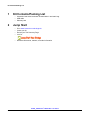
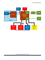
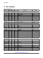
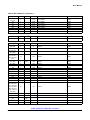
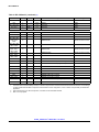
Freescale Semiconductor, Inc.
User’s Guide
Document Number: KT9Z1_638UG
Rev. 1.0, 3/2014
KIT9Z1J638EVM Evaluation Board
Featuring the MM9Z1J638 Intelligent Battery Sensor Module
Figure 1. KIT9Z1J638EVM Evaluation Board
Contents
1 Kit Contents/Packing List . . . . . . . . . . . . . . . . . . . . . . . . . . . . . . . . . . . . . . . . . . . . . . . . . . . . . . . . . . . . . 2
2 Jump Start . . . . . . . . . . . . . . . . . . . . . . . . . . . . . . . . . . . . . . . . . . . . . . . . . . . . . . . . . . . . . . . . . . . . . . . . . 2
3 Important Notice . . . . . . . . . . . . . . . . . . . . . . . . . . . . . . . . . . . . . . . . . . . . . . . . . . . . . . . . . . . . . . . . . . . . 3
4 Introduction . . . . . . . . . . . . . . . . . . . . . . . . . . . . . . . . . . . . . . . . . . . . . . . . . . . . . . . . . . . . . . . . . . . . . . . . 4
5 Evaluation Board Features . . . . . . . . . . . . . . . . . . . . . . . . . . . . . . . . . . . . . . . . . . . . . . . . . . . . . . . . . . . . 4
6 MM9Z1J638 Device Features . . . . . . . . . . . . . . . . . . . . . . . . . . . . . . . . . . . . . . . . . . . . . . . . . . . . . . . . . . 6
7 Required Equipment . . . . . . . . . . . . . . . . . . . . . . . . . . . . . . . . . . . . . . . . . . . . . . . . . . . . . . . . . . . . . . . . . 6
8 Evaluation Board Configuration. . . . . . . . . . . . . . . . . . . . . . . . . . . . . . . . . . . . . . . . . . . . . . . . . . . . . . . . . 7
9 Setting Up and Using the Hardware and Software . . . . . . . . . . . . . . . . . . . . . . . . . . . . . . . . . . . . . . . . . . 8
10 Schematic . . . . . . . . . . . . . . . . . . . . . . . . . . . . . . . . . . . . . . . . . . . . . . . . . . . . . . . . . . . . . . . . . . . . . . . 12
11 Board Layout . . . . . . . . . . . . . . . . . . . . . . . . . . . . . . . . . . . . . . . . . . . . . . . . . . . . . . . . . . . . . . . . . . . . . 14
12 Bill of Material . . . . . . . . . . . . . . . . . . . . . . . . . . . . . . . . . . . . . . . . . . . . . . . . . . . . . . . . . . . . . . . . . . . . 18
13 References . . . . . . . . . . . . . . . . . . . . . . . . . . . . . . . . . . . . . . . . . . . . . . . . . . . . . . . . . . . . . . . . . . . . . . 21
14 Revision History . . . . . . . . . . . . . . . . . . . . . . . . . . . . . . . . . . . . . . . . . . . . . . . . . . . . . . . . . . . . . . . . . . 22
© Freescale Semiconductor, Inc., 2014. All rights reserved.
Kit Contents/Packing List
1
Kit Contents/Packing List
•
•
•
2
Assembled and tested evaluation board/module in anti-static bag.
USB cable
Warranty card
Jump Start
•
•
•
•
Go to www.freescale.com/analogtools
Locate your kit
Review your Tool Summary Page
Look for
Jump Start Your Design
•
Download documents, software, and other information
KT9Z1_638UG User’s Guide Rev. 1.0 3/2014
2
Freescale Semiconductor
Important Notice
3
Important Notice
Freescale provides the enclosed product(s) under the following conditions:
This evaluation kit is intended for use of ENGINEERING DEVELOPMENT OR EVALUATION
PURPOSES ONLY. It is provided as a sample IC pre-soldered to a printed circuit board to make
it easier to access inputs, outputs, and supply terminals. This evaluation board may be used with
any development system or other source of I/O signals by simply connecting it to the host MCU
or computer board via off-the-shelf cables. This evaluation board is not a Reference Design and
is not intended to represent a final design recommendation for any particular application. Final
device in an application will be heavily dependent on proper printed circuit board layout and heat
sinking design as well as attention to supply filtering, transient suppression, and I/O signal quality.
The goods provided may not be complete in terms of required design, marketing, and or
manufacturing related protective considerations, including product safety measures typically
found in the end product incorporating the goods. Due to the open construction of the product, it
is the user's responsibility to take any and all appropriate precautions with regard to electrostatic
discharge. In order to minimize risks associated with the customers applications, adequate design
and operating safeguards must be provided by the customer to minimize inherent or procedural
hazards. For any safety concerns, contact Freescale sales and technical support services.
Should this evaluation kit not meet the specifications indicated in the kit, it may be returned within
30 days from the date of delivery and will be replaced by a new kit.
Freescale reserves the right to make changes without further notice to any products herein.
Freescale makes no warranty, representation or guarantee regarding the suitability of its products
for any particular purpose, nor does Freescale assume any liability arising out of the application
or use of any product or circuit, and specifically disclaims any and all liability, including without
limitation consequential or incidental damages. “Typical” parameters can and do vary in different
applications and actual performance may vary over time. All operating parameters, including
“Typical”, must be validated for each customer application by customer’s technical experts.
Freescale does not convey any license under its patent rights nor the rights of others. Freescale
products are not designed, intended, or authorized for use as components in systems intended
for surgical implant into the body, or other applications intended to support or sustain life, or for
any other application in which the failure of the Freescale product could create a situation where
personal injury or death may occur.
Should the Buyer purchase or use Freescale products for any such unintended or unauthorized
application, the Buyer shall indemnify and hold Freescale and its officers, employees,
subsidiaries, affiliates, and distributors harmless against all claims, costs, damages, and
expenses, and reasonable attorney fees arising out of, directly or indirectly, any claim of personal
injury or death associated with such unintended or unauthorized use, even if such claim alleges
that Freescale was negligent regarding the design or manufacture of the part.Freescale™ and the
Freescale logo are trademarks of Freescale Semiconductor, Inc. All other product or service
names are the property of their respective owners.
© Freescale Semiconductor, Inc. 2014
KT9Z1_638UG User’s Guide Rev. 1.0 3/2014
Freescale Semiconductor, Inc.
3
Introduction
4
Introduction
Freescale’s KIT9Z1J638EVM is a hardware tool for evaluation and development. It is ideal for rapid
prototyping of MCU-based applications for current, voltage and temperature sensing. The intelligent
battery sensor MM9Z1J638 hardware, KIT9Z1J638EVM, is a simple, yet sophisticated design featuring
an intelligent battery sensor with CAN and LIN.
KIT9Z1J638EVM can be used to evaluate the MM9Z1_638 family device. It features a MM9Z1J638,
integrating a S12Z MCU and a SMARTMOS analog control IC into a single-package solution. The
MM9Z1J638 enables precision measurement of key battery parameters, current, voltage and
temperature. The acquisitions are run through three 16-bit sigma-delta ADCs embedded into the analog
IC.
The MM9Z1J638 features a LIN protocol and physical interface compatible with LIN 2.0/2.1/2.2
requirements and MSCAN protocol controller and supply capability for 8 and 14 pin CAN interface.
The on-board interfaces include CAN, LIN. The CAN Physical Layer footprint allows to mount 8- or 14-pin
CAN interface; the connection of the physical layer to MM9Z1J638 is done through jumpers to allow each
configuration.
The KIT9Z1J638EVM is featuring Open Source BDM (OSBDM) providing low-speed debug
communications to the S12Z core.
5
Evaluation Board Features
The KIT9Z1J638EVM evaluation board demonstrates the MM9Z1J638 multi-chip module IC. The board’s
main features are as follows:
•
•
•
•
•
•
•
MM9Z1J638 intelligent battery sensor in a 48-QFN package with wettable flank
High-speed CAN interface using MC33901, high-speed CAN transceiver and msCAN protocol layer
embedded into the MM9Z1J638
LIN interface
Customizable GPIOs for voltage and temperature sensing
LED indicators
Onboard BDM connection via open source OSBDM circuit using the MC9S08JM60 MCU.
Support for external BDM interface (for instance P&E USB Multilink BDM interface)
KT9Z1_638UG User’s Guide Rev. 1.0 3/2014
4
Freescale Semiconductor
Evaluation Board Features
External
BDM Port
GND/VBAT
Rx
Mini-B
USB
BKGD
USB
D+/D-
RESET
MC9S08JM60
msCAN
Tx
CANH
MC33901
Intelligent Battery
Sensor
MM9Z1J638
48 QFN
LIN
PHY
CANL
CANL
LIN
DB9 CAN
Connector
LIN
Connector
OSBDM
Current Sense
Input Pins
ISENSEL
/
ISENSEH
Voltage Sense
Input Pins
VSENSE[3..0]
Voltage Sense
Input Pins
PTB[4..0]
External
Temperature
Sense Input
Pins
PTB[4..0]
Figure 2. KIT9Z1J638EVM Block Diagram
KT9Z1_638UG User’s Guide Rev. 1.0 3/2014
Freescale Semiconductor, Inc.
5
MM9Z1J638 Device Features
6
MM9Z1J638 Device Features
The MM9Z1J638 is a fully integrated intelligent battery sensor device. The device supports precise
current measurement via an external shunt resistor. It features four voltage measurements via an internal
calibrated resistor divider or use of an external divider. Specific device functions include the following:
•
•
•
•
•
•
•
•
•
•
7
Wide range battery current measurement; on-chip temperature measurement
Four battery voltage measurements with internal resistor dividers, and up to five direct voltage
measurements for use with an external resistor divider
Measurement synchronization between voltage channels and current channels
Five external temperature sensor inputs with internal supply for external sensors
Low-power modes with low-current operation
Multiple wake-up sources: LIN, timer, high-voltage input, external CAN interface, and current
threshold and integration
Precision internal oscillator and connections for external crystal
LIN 2.2/2.1/2.0 protocol and physical interface
MSCAN protocol controller, and supply capability for 8 and 14-pin CAN interfaces
S12Z microcontroller with 128 kByte Flash, 8.0 kByte RAM, 4.0 kByte EEPROM
Required Equipment
Minimum equipment required:
•
•
•
•
DC power supply with 12 V voltage capability and 300 mA current capability
Oscilloscope (preferably four-channel)
Digital multimeter
USB-enabled PC with Windows XP or higher and CodeWarrior 10.x installed
KT9Z1_638UG User’s Guide Rev. 1.0 3/2014
6
Freescale Semiconductor
Evaluation Board Configuration
8
Evaluation Board Configuration
Switch S1
PTB Thermal Sense
LED D6
PTB Voltage Sense
LED D7
PTB4
Ext WU
BDM
Connector
VSENSE3
USB
VSENSE2
OSBDM
Connector
VSENSE1
CAN Transceiver (U2)
VSENSE0
CAN Connector
ISENSEH
LIN Connector
ISENSEL
GND
VBAT
Power Supply
Figure 3. KIT9Z1J638EVM Board Setup
When using the OSBDM USB interface,
set the following S1 switch settings:
When using the BDM connector,
set the following S1 switch settings:
Figure 4. Switch S1 Settings
KT9Z1_638UG User’s Guide Rev. 1.0 3/2014
Freescale Semiconductor, Inc.
7
Setting Up and Using the Hardware and Software
9
Setting Up and Using the Hardware and Software
In order to perform the demonstration examples, first setup the evaluation board hardware and software
as follows:
1. Download CodeWarrior 10.4 or higher, using the instructions in the “Jump Start” section.
2. Install CodeWarrior Suite on to a USB-enabled PC running Windows XP or higher.
3. Connect the USB cable from the OBSDM port on the evaluation board to computer.
4. Without turning on the power, connect the positive voltage output (set for +12V) of the DC power
supply to the VBAT terminal on the board (schematic label CN5). Connect the ground line from the
supply to the GND terminal on the board (CN6).
5. Launch the CodeWarrior Suite.
6. Turn on the power supply.
7. Start development of your application using CodeWarrior.
Notes:
1. Notice on the EVM, for proper operation connect RESET to RESETA, by setting pin 1 of the S1 Switch
ON. The S1 switch is not always set, because when flashing the part, there is flow between the reset
drive from the BDM interface and the reset from the analog die (through the watchdog). A workaround
is to add a 470 nF capacitor between RESET and GND on the BDM interface. This prevents resets
while flashing. Disconnecting both pins through the switch S1-1 on KIT9Z1J638EVM avoids this
workaround.
2. The RESET pin of the MM9Z1J638 is a reset Input/Output pin of the embedded MCU, so when
hitting BP1, the embedded MCU will be reset. RESETA pin of MM9Z1J638 is a reset output (when in
normal mode), so setting RESETA pin to 0 will not reset the analog die. This must be done through
the HWR bit of the PCR_CTL register. Each time there is a RESET of the MCU, check that the
HWRF bit is set. If not, a command reset to the analog die through HWR of PCR_CTL is needed.
9.1
GPIO Setup
The KIT9Z1J638EVM is offering a customizable set of general purpose IOs for measurement of external
temperature or voltage through the dedicated 16-bit sigma-delta ADCs of the MM9Z1J638, intelligent
battery sensor.
The customization must be performed by setting the right set of components on the selected PTB.
Footprints and dedicated banana connectors are available on the board to customize the
KIT9Z1J638EVM according to your application needs.
•
•
•
PTB[3…1] can also be set as 5.0 V IOs which might be connected to TIMer and/or SCI (UART)
modules.
PTB4 can be set as a 5.0 V input and offers extra functionalities such as a CAN wake-up pin and high
voltage wake-up input pin.
PTB5 is a ground switch and is used while monitoring external temperatures to minimize power
consumption.
Refer to the schematics in Figure 5.
KT9Z1_638UG User’s Guide Rev. 1.0 3/2014
8
Freescale Semiconductor
Setting Up and Using the Hardware and Software
PTB[4…0] Voltage Sensing External
Divider with R1 and R2
PTB[4…0] External Temperature
Sensing Thermistor RT
Figure 5. Using GPIOs as Voltage Sense or External Temperature Sense Inputs
Refer to the MM9Z1_638D1 data sheet for further information regarding voltage and external temperature
sensing. Refer to Figure 8 for the component for every GPIO.
Refer to Assembly Layer Top for the localization of components and footprint on the KIT9Z1J638EVM.
Note: GPIO pins might also be connected to OSBDM to set Serial to the USB port. This is done by
connecting:
TxD from SCI to one pin out of PTB[3…1], then the selected PTB to JP4-2.
RxD from SCI to one pin out of PTB[4…1], then the selected PTB to JP4-1.
Insure that the two selected PTB pins have no other setting (voltage sensing external divider, external
temperature sensing setup), which might conflict with the 5.0 V digital IO setup.
9.2
CAN Configuration
The KIT9Z1J638EVM board comes with an 8-pin high-speed CAN transceiver MC33901, mounted in the
U2 position.This transceiver is configured using jumpers JM1 to JM9.
The KIT9Z1J638EVM is highly configurable to set the product within the configuration closest to designer
needs, and showcases the versatility of the MM9Z1_638 product. It allows using an 8-pin (without SPLIT
pin version) or a 14-pin CAN transceiver as a CAN transceiver. This is done by setting the device in the
U2 position on the board, according to Figure 6, and to connect pins through the jumpers as shown in
Figure 7.
KT9Z1_638UG User’s Guide Rev. 1.0 3/2014
Freescale Semiconductor, Inc.
9
Setting Up and Using the Hardware and Software
U2 mounted with 8-pin
CAN transceiver
U2 mounted with 14-pin
CAN transceiver
Figure 6. CAN Transceiver Placement
The connection between CAN transceiver is configured using the jumpers JM1 to JM9. There is one
configuration for 8 pins and two for 14 pins.
8-pin CAN operation
14-pin CAN operation:
Low-power mode = sleep
mode on MM9Z1J638 - WU
through INH
14-pin CAN operation:
Low-power mode = stop
mode on MM9Z1J638 - WU
through RxD
Note: Jumpers in orange have to be connected for proper operation
Figure 7. CAN Jumper Connections
9.3
Hardware Description
This evaluation kit features one MM9Z1J638 (intelligent battery sensor), one MC33901 (high-speed CAN
Interface), and one MC9S08JM60CQH (OSBDM debug interface). The board-level logic diagram is show
in Figure 2.
9.4
LED Display
The following LEDs are provided as visual output devices for the KIT9Z1J638EVM evaluation board:
1. LED D3 indicates when switch S3-2 is ON and PA6 is set to 5.0 V
2. LED D4 indicates when switch S3-1 is ON and PA7 is set to 5.0 V
3. LED D6 indicates when OSBDM is powered by a USB cable
4. LED D7 indicates when OSBDM is connected to the MM9Z1J638 through S1-2, S1-3, S1-4, and the
MM9Z1J638 is powered through VBAT and GND connections
KT9Z1_638UG User’s Guide Rev. 1.0 3/2014
10
Freescale Semiconductor
Setting Up and Using the Hardware and Software
9.5
Test Point Definitions
The following test-point jumpers provide access to signals on the KIT9Z1J638EVM IC:
Table 1. Test Point Jumpers and Description
Test Point Number
Description
TP1
PA7
TP2
VDDL
TP3
PTB0
TP4
PTB1
TP5
PTB2
TP6
PTB3
TP7
PA6
TP8
PA5
TP9
PA4
TP10
VSENSE3
TP11
VSEMSE2
TP12
VSENSE1
TP13
VSENSE0
TP14
ISENSEH
TP15
ISENSEL
TP16
PTB4
TP17
PTB5
TP18
VDDX
TP19
VDDH
TP20
VSUP
TP21
LIN
TP22
VDDA
TP23
ELE_PS_SENSE
TP24
RESET
TP25
RESETA
TP26
GND
TP27
GND
TP28
GND
TP29
GND
TP30
GND
TP31
GND
TP32
GND
TP33
GND
TP34
GND
TP35
CANH
TP36
CANL
KT9Z1_638UG User’s Guide Rev. 1.0 3/2014
Freescale Semiconductor, Inc.
11
A
CAN8_VIO
C5
18pf - dnp
2
4
6
8
10
12
GND
GND
D4
LED
R24
2.2k
PA7_LED
1
3
4
GND
2
1
R25
47k
STBb
CANH
CANL
SPLIT
VBAT
WAKE
ERRb
TJA1041 - dnp
TXD
GND
VCC
RXD
VIO
EN
INH
U2
dtsmw-69n
BP2
SW DIP-2
S3
PE0
PA6
PA4
PA2
PA0
GND
2
4
6
PA2
PA1
PA0
0
13
14
GND
TP18
TSTPT
11
12
1
2
3
4
5
6
7
8
9
10
GND
2
GND
VSSRX
VDDRX
TP33
TSTPT - dnp
GND
1
6
2
7
3
8
4
9
5
GND
GND
EXPOSE
C12
470nF
VDDX
PA5
PA1
DB9 - dnp PA4
J5
C13
47nF
TSTPT
GND
TP20
TP21
TSTPT
TSTPT
GND
U1
3
36
35
34
33
32
31
30
29
28
27
26
PCB
PCB
JM5
PCB
JM4
PCB
JM3
JM2
TP17
TSTPT
TSTPT
TSTPT
TP14
TP15
TSTPT
TSTPT
TP16
3
CAN_EN
CAN_RXD
CAN_5V
CAN_TXD
GND
GND
PTB4
PTB5
GND
ISENSEH
ISENSEL
EXT_WU
VSUP
PA0
R12
1.8k
PCB
PCB
JM9
PCB
JM8
PCB
JM7
VSUP
BP3
CAN_RXD
CAN_VSUP
CAN_STBb
2.2n
C14
4
D5
5.1V
R26
47k
GND
C19
2.2n
1k
R35
GND
R16
3.6k
BANANA_BLUE
2.2k - dnp
100k - dnp
R30
2.2k
R29
100k
R28
PTB5_T_INPUT
GND
5
Date:
File:
B
Size
Title
BANANA_BLUE
CN22
3
4
SW DIP-2
S2
Number
CN16
2.2k
Revision
mm912_638_evb_osbdm
mm912_638_evb_osbdm.sch
BANANA_RED
CN23
BANANA_RED
R36
CN18
BANANA_RED
CN17
2.2k
2PTS
JMP2
BANANA_BLACK
BANANA_RED
CN13
0
BANANA_RED
0
R22
CN12
R21
2
BANANA_GREEN
R33
1
2.2k
R32
2.2k
R31
GND
C16
dnp
C10
dnp
VSUP
C4
100nF
GND
CN11
C28
220pF
GND
GND
C3
4.7uF
GND
CN6
BANANA_BLACK
A
B
C
D
6
30-Jan-2012
Sheet of
\\tls-file01\tls_ampd\products_auto\NPI\QuIBSplus\6_Application_Customer\2-hardware\evb\mm9
Drawn By:
VSENSE3
VSENSE2
dnp
R20
0
R11
C9
dnp
GND
VSUP
VSENSE1
VSENSE0
2
1
SS2P5-E3/84A - dnp
D2
SS2P5-E3/84A
D1
CN5
BANANA_RED
PTB5_T_INPUT
BANANA_YELLOW
10k
CN15
RT5
BANANA_BLUE
CN14
GND
BANANA_YELLOW
100k
6
MM912_638 Power Supply
PTB5_T_INPUT
10k - dnp
CN10
R19
RT4
CN9
R18
R27
1.8k - dnp
C15
2.2n
GND
VDDA
CN21
BANANA_GREEN
EXT_WU
GND
PTB5
dtsmw-69n
GND
JMP1
PTB4
BANANA_YELLOW
100k
C8
2.2n
GND
PTB3
100k - dnp
BANANA_YELLOW
100k - dnp
PTB5_T_INPUT
10k
CN4
R10
VDDA
GND
R17
BANANA_BLUE
RT2
CN3
2.2k
5
R9
100k
R8
R7
1.8k - dnp
C2
2.2n
GND
PTB1
VDDA
PTB5_T_INPUT
10k - dnp
CN8
RT3
BANANA_BLUE
R15
2.2k - dnp
R14
100k - dnp
CAN_INH
GND
JM6
GND
PTB2
VDDA
CN7
BANANA_YELLOW
100k - dnp
R13
4
PTB5_T_INPUT
10k
CN2
R6
EXT_WU
GND
C7
2.2n
BANANA_BLUE
2.2k
RT1
CN1
R5
100k
R4
R3
1.8k - dnp
C1
2.2n
GND
PTB0
VDDA
VSENSE3 TP10
TP11
VSENSE2 TSTPT
TP12
VSENSE1 TSTPT
TP13
VSENSE0 TSTPT
1000
GND
MM912_638
TP22
VSENSE3
VSENSE2
VSENSE1
VSENSE0
ADCGND
ISENSEH
ISENSEL
GNDSUB
PTB4_L0
PTB5_GND_SW
AGND
GND
C11
1uF
GNDGND
TP19
TSTPT
R34
120 - dnp
TP32
TSTPT - dnp
VSS1
NC
GND
GND
TP2 TP3TP4TP5TP6
TSTPTTSTPT
TSTPT
TSTPT
TSTPT
GND
TP26 TP27 TP28 TP29 TP30 TP31
TSTPTTSTPTTSTPTTSTPTTSTPTTSTPT
TP1 TP24
TP25
TSTPTTSTPT
TSTPT
PA6
EXTAL
XTAL
TEST
PA5
PA4
PA3/SS
PA2/SCK
PA1/MOSI
PA0/MISO
dtsmw-69n
BP1
GND
GND
TP8
PA5
TP9
PA4
TSTPT
PA3
TSTPT
TSTPT
TP7
PA6
GND
VDDX
14 CAN_STBb
CANH
13
CANL
12
11 CAN8_VIO
CAN_VSUP
10
9
GND
C18
8
2.2u - dnp
PA7
VDDX
PA6
PA7
PE0
PE1
BDM_EXT
1
3
5
JP1
C6
18pf - dnp
PE1
RESET_A
BKGD
GND
HEADER 6X2
1
3
5
7
9
11
CON1
8
7
6
5
4MHz - dnp
X1
SW DIP-4
S1
CAN_TXD1
JM1
2
PCB GND
CAN_5V
3
CAN_RXD4
C17
5
4.7u - dnp CAN_EN 6
CAN_INH 7
GND
GND
D3
LED
R23
2.2k
PA6_LED
PE1
PA7
PA5
PA3
PA1
VDDX
PE0
RESET 1
2
TRG_RST
TBGND 3
V_TRG 4
3.3k
R1
RESET
ISENSEL
B
C
D
VDDX
2
PA7
BKGD
RESET
RESET_A
VDDH
R2
VDDL
VDDX
1
PTB0
PTB1
PTB2
PTB3
48
47
46
45
44
43
42
41
40
39
38
37
PA7
BKGD
RESET
RESET_A
DGND
TEST_A
VDDL
GNDSUB
PTB0_TCLK
PTB1
PTB2
PTB3
VDDD2D
NC
DGND
VDDH
GNDSUB
VDDX
NC
VSUP
LIN
LGND
VDDA
15
16
17
18
19
20
21
22
23
24
25
VSUP
LIN
ISENSEH
VDDA
VBAT
LIN
PTB4_WU
1
PTB4
2
PTB4_SENSE
3
12
BDM connector
Schematic
10 Schematic
Figure 8. Evaluation Board Schematic, Part 1
KT9Z1_638UG User’s Guide Rev. 1.0 3/2014
Freescale Semiconductor
A
B
C
D
J3
USB1
GND
1
R37
TBGND_OUT
4.7k
TBGND_IN
GND
A
VCCA
R50
10K
UVDD
USBDN
USBDP
NC
UGND
5
3
1
6
4
2
1
2
3
4
5
+
C31
10uf
GND
USBDN
USBDP
GND
10uf
0.1uf
C34
5VUSB
C33
1nf
R51
10K
GND C32
33-1%
33-1%
R52
10k
5VUSB
FERRITE BEAD
L2
R60
C30
1uf
5
4
6
R38
10k
5VUSB
OS_RESET
5VUSB
6
4
2
GND
R59
OS_DEBUG
5
3
1
J2
GND
2
BOOTLOADER_ENABLE
J1
OS_BKGD
1
OSBDM and MCUID VERSIONING
R49
10K
DIR
B
VCCB
SN74LVC1T45
OSBDM_REV2
OSBDM_REV1
OSBDM_REV0
GND
2
3
1
TBGND
TBGND_EN
4
5
6
7
8
9
VPP_EN
TBGND_IN
TBGND_OUT
TBGND_EN
TXD
RXD
5VUSB
2
VTRG_FAULT
5VSW_FAULT
19
USBDP
R42
10k
GND
GND
R43
10k
GND
VSSOSC
PTC0/SCL
PTC1/SDA
PTC2
PTC3/TxD2
PTC5/RxD2
PTG2/KBIP6
PTG3/KBIP7
BGND/MS
PTG4/XTAL
PTG5/EXTAL
GND
PTB0/MISO2/ADP0
PTB1/MOSI2/ADP1
PTB2/SPSCK2/ADP2
PTB3/SS2/ADP3
PTB4/KBIP4/ADP4
PTB5/KBIP5/ADP5
PTD0/ADP8/ACMP+
PTD1/ADP9/ACMP-
VDDAD/VREFH
VSSAD/VREFL
PTD2/KBIP2/ACMP0
R45
10k
3
4
1
7
2
R46
10k
5VUSB
VTRG_FAULT
MC9S08JM60 44P1N
PTG1/KBIP1
PTG0/KBIP0
VUSB33
USBDP
USBDN
VSS
VDD
PTE7/SS1
PTE6/SPSCK1
PTE5/MOSI1
PTE4/MISO1
PTE3/TPM1CH1
PTE2/TPM1CH0
PTE1/RxD1
PTE0/TxD1
PTF5/TPM2CH1
PTP2/TPM2CH0
PTP1/TPM1CH3
0.1uf
C20
5VSW_EN
GND
VTRG_EN R44
2.2k
5VSW_FAULT
GND
PTP0/TPM1CH2
RESET
IRQ/TPMCLK
PTC4
U7
C35
C36
0.01UF 0.1UF
22
21
20
18
USBDN
17
16
15
14
13
12
11
10
3
2
1
OS_RESET
TRESET_OUT
R53
R54
TBD 1% TBD 1%
BRD_ID0
BRD_ID1
R40
R41
TBD 1% TBD 1%
47
R39
V_TRG
3
43
44
23
24
25
26
27
28
29
30
31
32
33
34
35
36
37
38
39
40
41
42
GND
BOUT
AOUT
5VSW_EN
VTRG_EN
BRD_ID0
BRD_ID1
VTRG_IN
6
5
8
100nf
5VUSB
C37
TRESET_IN
OS_BKGD
O_XTAL
O_EXTAL
GND
OSBDM_REV0
OSBDM_REV1
OSBDM_REV2
VPP_ON
GND
10k
R47
ELE_PS_SENSE
TSTPT
TP23
MIC2026
FLGB
FLGA
ENB
ENA
IN
U4
STATUS-green
GND
1
1
U5
PDTC115T
GND
R62
10k
R55
1k
D6
5VUSB
GND
5V_SW
C21
10uF
+
GND
RXD
TXD
GND
4
GND
GND
5V_SW
GND
5V_SW
2
3
1
2
3
1
DIR
B
DIR
B
VCCB
SN74LVC1T45
GND
A
VCCA
U10
4
5
GND
C23
100pf
3V_TRG
5
4
6
5
4
6
GND
5
TXD_VIRTUAL_TOT
V_TRG
5V_SW
RXD_VIRTUAL_TOT
V_TRG
3V regulator is optional
NR
OUT
VCCB
SN74LVC1T45
GND
A
VCCA
U9
POWER GENERATOR
GND
EN
IN
U6
TPS79933
+ C22
10μF
3
1
5V_TRG
VIRTUAL SERIAL PORT
C38
100nf
R63
10k
V_TRG
R56
1k
D7
GND
2
GND
2
U3
3
3
2
TPWR-yellow
5V_SW
5
GND
CON2
1
2
J4
+ C24
10μF
C25
18pf
TRESET_IN
GND
R73
10k
GND
4MHz
X2
1M
R48
TRESET_OUT
O_EXTAL
10k
R74
VPP_EN
C26
18pf
6
O_XTAL
6
R75
10k
5V_SW
TRG_RST
GND
R65
10k - dnp
R64
10k - dnp
4.7k - dnp
GND
Q4
3904
47
R66
R58
10k - dnp
3
100 - dnp
R67
C39
1nf - dnp
BAT54C - dnp
2
1
Q3
3904
GND
GND
V_TRG
2
D10
3904 - dnp
Q1
R57
JMP3 1
2PTS - dnp
GND
2
1
4
3
GND
7
10k
R77
10k
R76
D11
BAT54C
TRG_RST
4.7k - dnp
R69
4
5
GND
R70
10k - dnp
1
2
EN
VIN
U8
TPS61041 - dnp
GND
R78
10k
V_TRG
FB
SW
10uH - dnp
5V_SW
L1
1
2
12V VPP GENERATION
GND
VPP_ON
10uf - dnp
C27
+
BAT54C - dnp
3
D8
7
Q2
3906 - dnp
3
R68
1k - dnp
3
3
BGND SWITCH
3
2
2
1
1
+
2
GND
Freescale Semiconductor, Inc.
2
1
1
C29
dnp
R72
GND
RESET OUT/IN
Q5
3906
GND
10k
R79
C40
1uf - dnp
9.09k - dnp
R71
1k - dnp
V_TRG
3
SS12 - dnp
D9
8
8
GND
A
B
C
D
Schematic
Figure 9. Evaluation Board Schematic, Part 2
KT9Z1_638UG User’s Guide Rev. 1.0 3/2014
13
Board Layout
11 Board Layout
11.1
Assembly Layer Top
KT9Z1_638UG User’s Guide Rev. 1.0 3/2014
14
Freescale Semiconductor
Board Layout
11.2
Assembly Layer Bottom
Note: This image is an exception to the standard top-view mode of representation used in this document. It has been
flipped to show a bottom view.
KT9Z1_638UG User’s Guide Rev. 1.0 3/2014
Freescale Semiconductor, Inc.
15
Board Layout
11.3
Top Layer Routing
KT9Z1_638UG User’s Guide Rev. 1.0 3/2014
16
Freescale Semiconductor
Board Layout
11.4
Bottom Layer Routing
Note: This image is an exception to the standard top-view mode of representation used in this document. It has been
flipped to show a bottom view.
KT9Z1_638UG User’s Guide Rev. 1.0 3/2014
Freescale Semiconductor, Inc.
17
Bill of Material
12 Bill of Material
Table 2. Bill of Material (1)
Schematic Label Quantity Assy. Opt.
Value
Description
Package
Integrated Circuits
(2)
U1
1
Freescale MM912J638BM2EP
QFN48LD-EP
U2
1
Freescale MC33901WEF (SO-8)
SO-14
U3
1
SN74LVC1T45DBVR
SOT-23-6
U4
1
MIC2026-1YM
SOIC-8
U5
1
PDTC115T
SOT-23
U6
1
TPS79933
TSOT-23−5
Freescale MC9S08JM60CQH
QFP44
TPS61041
SOT-23-5
SN74LVC1T45
SOT-23-6
4.0 MHz HC-49/SMT
HC-49 SMD
U7
1
U8
1
U9, U10
2
(2)
DNP
(3)
Crystal Oscillators
X1, X2
2
4.0 MHz
Transistors
Q1
1
DNP (3)
MMBT3904
SOT-23
Q2
1
DNP (3)
MMBT3906
SOT-23
Q3, Q4
2
MMBT3904
SOT-23
Q5
1
MMBT3906
SOT-23
Diodes (including LEDs)
D1, D2
2
SS2P5-E3/84A
SMP
D3, D4
2
HSMH-C170
D0805
D5
1
BZX384-C5V1,115
SOD323
D6
1
STATUS GREEN
D1206
D7
1
TPWR YELLOW
D1206
D8
1
DNP (3)
BAT54C, 215
SOT-23
(3)
SS12
DO-214AC (SMA)
BAT54C
SOT-23
BAT54C
SOT-23
2.2 nF
50V Capacitor
C0805
5.1 V
D9
1
DNP
D10
1
DNP (3)
D11
1
Capacitors
C1, C2, C7, C8,
C14, C15, C19
7
C3
1
4.7 μF
100V Capacitor
c2220
C4, C37, C38
3
100 nF
50V Capacitor
C0805
C5, C6, C25, C26
4
18 pF
50V Capacitor
C0805
C9, C10, C16,
C29
4
—
DNP Capacitor
C0805
C11, C30
2
1.0 μF
50V Capacitor
C0805
C12
1
470 nF
100V Capacitor
C0805
C13
1
47 nF
100V Capacitor
C0805
C17
1
4.7 μF
16V Capacitor
C0805
C18
1
2.2 μF
100V Capacitor
C1210
C20, C34, C36
3
0.1 μF
50V Capacitor
C0805
DNP (3)
KT9Z1_638UG User’s Guide Rev. 1.0 3/2014
18
Freescale Semiconductor
Bill of Material
Table 2. Bill of Material (continued) (1)
Schematic Label Quantity Assy. Opt.
C21, C22, C24,
C31, C32
5
C23
1
(3)
Value
Description
Package
10 μF
10V Capacitor
C0805
100 pF
50V Capacitor
C0805
C27
1
10 μF
10V Capacitor
C0805
C28
1
220 pF
100V Capacitor
C0805
C33
1
1.0 nF
50V Capacitor
C0805
C35
1
0.01 μF
100V Capacitor
C0805
C39, C40
2
DNP (3)
1.0 nF
50V Capacitor
C0805
L1
1
DNP (3)
10μH
Choke Coil ELL6SH100M
L2
1
DNP
Inductors
Ferrite Bead BLM21PG331SN1D
L0805
Resistors
R1
1
3.3 k
Resistor
R0805
R2, R11, R21,
R22, R54
5
0
Resistor
R0805
R3, R7, R27
3
1.8 k
Resistor
R0805
R4, R8, R15,
R19, R28
5
100 k
Resistor
R0805
R5, R9, R23,
R24, R29, R31,
R32, R33, R36,
R44
10
2.2 k
Resistor
R0805
R6, R10, R13,
R17, R30
5
100 k
Resistor
R0805
R12, R53
2
1.8 k
Resistor
R0805
DNP (3)
DNP (3)
(3)
R14, R18
2
2.2 k
Resistor
R0805
R16
1
3.6 k
Resistor
R0805
R20
1
DNP
Resistor
R0805
R25, R26
2
47 k
Resistor
R0805
R34
1
120
Resistor
R0805
R35, R55, R56
3
1.0 k
Resistor
R0805
R37
1
4.7 k
Resistor
R0805
R38
1
10 k
Resistor
R0805
R39, R66
2
47
Resistor
R0805
R40, R41, R42,
R43, R45, R46,
R47, R49, R50,
R51, R52, R62,
R63, R73, R74,
R75, R76, R77,
R78, R79
20
10 k
Resistor
R0805
DNP
R48
1
1.0 M
Resistor
R0805
R57, R69
2
DNP (3)
4.7 k
Resistor
R0805
R58, R64, R65,
R70
4
DNP (3)
10 k
Resistor
R0805
R59, R60
2
33
Resistor
R0805
R67
1
DNP (3)
100
Resistor
R0805
KT9Z1_638UG User’s Guide Rev. 1.0 3/2014
Freescale Semiconductor, Inc.
19
Bill of Material
Table 2. Bill of Material (continued) (1)
Schematic Label Quantity Assy. Opt.
R68, R71
2
DNP (3)
(3)
R72
1
RT1, RT2, RT5
3
RT3, RT4
2
DNP
DNP (3)
Value
Description
Package
1.0 k
Resistor
R0805
9.09 k
Resistor
R0805
10 k
Thermistor
R0805
10 k
Thermistor
R0805
Switches, Connectors, Jumpers and Test Points
BP1, BP2, BP3
3
Tactile Switch DTSMW-69N
DTSMW69
S1
1
SWITCH
DIP-8
S2, S3
2
SWITCH
DIP-4
CN1, CN3, CN7,
CN9, CN14,
CN22
6
BANANA BLUE
Banana connector 4.0 mm
CN2, CN4, CN8,
CN10, CN15
5
BANANA YELLOW
Banana connector 4.0 mm
CN5, CN12,
CN16, CN17,
CN18, CN23
6
BANANA RED
Banana connector 4.0 mm
CN6, CN13
2
BANANA BLACK
Banana connector 4.0 mm
CN11, CN19,
CN20, CN21
4
BANANA GREEN
Banana connector 4.0 mm
CON1
HEADER CON 6x2 2.54mm
J1
1
JUMPER CON 2 2.54mm (BOOTLOADER_ENABLE)
J2
1
JUMPER CON HE-10 6 MD (OS_DEBUG)
J3
1
USB Connector 5P MINI TYPE B RECPT
J4
1
JUMPER CON 2 2.54mm
J5
1
CONNECTOR DB9 Female
JM1 - JM9
9
JUMPER PCB
JMP1
1
JUMPER PTB4 CON 3 2.54mm
JMP2, JMP3
2
JUMPER 2PTS CON 2 2.54mm
JP1
1
JUMPER CON HE-10 6 MD (BDM_EXT)
TP1 - TP33
33
TSTPT 5000
SMT WITH POSTS
Notes
1. Freescale does not assume liability, endorse, or warrant components from external manufacturers that are referenced in circuit drawings
or tables. While Freescale offers component recommendations in this configuration, it is the customer’s responsibility to validate their
application.
2. Critical Components. For critical components, it is vital to use the manufacturer listed.
3. DNP = Do not populate
KT9Z1_638UG User’s Guide Rev. 1.0 3/2014
20
Freescale Semiconductor
References
13 References
Following are URLs where you can obtain information on related Freescale products and application
solutions:
Freescale.com
Support Pages
Description
URL
KIT9Z1J638EVM
Tool Summary Page
http://www.freescale.com/webapp/sps/site/prod_summary.jsp?code=KIT9Z1J638EVM
MM9Z1J638
Product Summary Page
http://www.freescale.com/webapp/sps/site/prod_summary.jsp?code=MM9Z1_638
MM9Z1_638
Data Sheet
http://www.freescale.com/files/analog/doc/data_sheet/MM9Z1_638D1.pdf
Analog Home Page
Home Page
http://www.freescale.com/analog
Battery Home Page
Home Page
http://www.freescale.com/battery
OSBDM Source Code Home Page
13.1
http://www.pemicro.com/osbdm
Support
Visit www.freescale.com/support for a list of phone numbers within your region.
13.2
Warranty
Visit www.freescale.com/warranty for a list of phone numbers within your region.
KT9Z1_638UG User’s Guide Rev. 1.0 3/2014
Freescale Semiconductor, Inc.
21
Revision History
14 Revision History
Revision
Date
1.0
3/2014
Description of Changes
• Initial Release
KT9Z1_638UG User’s Guide Rev. 1.0 3/2014
22
Freescale Semiconductor
How to Reach Us:
Information in this document is provided solely to enable system and software implementers to use Freescale products.
Home Page:
freescale.com
There are no express or implied copyright licenses granted hereunder to design or fabricate any integrated circuits based
Web Support:
freescale.com/support
Freescale reserves the right to make changes without further notice to any products herein. Freescale makes no
on the information in this document.
warranty, representation, or guarantee regarding the suitability of its products for any particular purpose, nor does
Freescale assume any liability arising out of the application or use of any product or circuit, and specifically disclaims any
and all liability, including without limitation consequential or incidental damages. “Typical” parameters that may be
provided in Freescale data sheets and/or specifications can and do vary in different applications, and actual performance
may vary over time. All operating parameters, including “typicals,” must be validated for each customer application by
customer’s technical experts. Freescale does not convey any license under its patent rights nor the rights of others.
Freescale sells products pursuant to standard terms and conditions of sale, which can be found at the following address:
freescale.com/SalesTermsandConditions.
Freescale and the Freescale logo are trademarks of Freescale Semiconductor, Inc., Reg. U.S. Pat. & Tm. Off.
SMARTMOS is a trademark of Freescale Semiconductor, Inc. All other product or service names are the property of their
respective owners.
© 2014 Freescale Semiconductor, Inc.
Document Number: KT9Z1_638UG
Rev. 1.0
3/2014