1
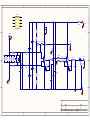
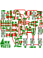
Application Note TP5532
TP5532 Evaluation Board User’s Guide Description
The TP5532 evaluation board contains a complete
precision current sense amplifier using the TP5532
chopper amplifier in a high side, low side of floating
supply current sense application.
The advantages of the TP5532 in this application include
which filter the noise generated by power supply. Reverse
polarity protection uses the 100Ω resistor and two
protection diode pairs (D3, D4). These also provide input
common mode voltage protection to the op amp.
Input Protection Clamp Options very low offset voltage (2μV typical) and offset drift
Included on the evaluation board are optional input
(0.008μV/°C), rail-to-rail input and output and low power
protection circuits that illustrate the best methods to limit
consumption (34μA per Amplifier typical). These features
input common mode and differential transient voltage
provide a very high degree of precision for use in 5V, low
spikes in exposed or electrically hazardous applications.
power applications.
The TP5532 can handle input common mode and
differential transients to a diode drop beyond the rails, or
Evaluation Board Key Features
The TP5532 EVB operates from a single 1.8VDC to
+5.5VDC supply. The current sense function is configured
as a single stage, balanced input, trans-impedance
amplifier. A 0.1Ω 0.1% current sense resistor is used
convert the incoming current to a voltage which is applied
to a precision differential amplifier with a gain of 100. The
overall current to voltage transfer ratio is 10V/A, and a
bidirectional current range of ±0.25A is achieved when
operating from a +5V supply, using a 2.5V reference
voltage (VREF). At +25°C, the TP5532 achieves a total full
scale offset error of 0.038% (when a precision external
reference is used) and approximately 0.15% using the
internal 0.1% resistors. The total current draw from the
amplifier power is less than 35μA and the total leakage
current from the current sense input is less than 3μA.
Power Supply and Protection
Features
External power connections are made through the +V,
and ground jacks. The single supply input is overvoltage
protected using a series 100Ω (R15) resistor and a 5.6V
zener diode (D1). R15 is used to reduce the overvoltage
from power supply, D1 is used to protect the chip from
overvoltage, allows over current flows through it to ground.
R15, C4 and C2 all works together as a RC low pass filter
www.3peakic.com
to a range of -0.5V to +5.5V when operating from a single
5V supply. Clamp diodes D3A, B, D4A, B and input
resistors R6, R7, R8, R9 form a current limiting, 6V
common mode and differential voltage clamp. This clamp
provides sufficient protection for the TP5532 for common
mode fault voltages far beyond the power supply rails.
These diodes also provide the same 6V protection
against large differential transients. High speed current
sensing may involve filtering repetitive current transients
with high peak to average values. In these cases, limiting
these transient even further will improve amplifier
response and overload settling time. The optional
Schottky diode transient clamp D2 reduces transients let
through by the common mode clamp from 6V down to ~
±0.3V,
which
improves
overload
recovery
time.
Capacitors C7 and C9 provide common mode noise
filtering and capacitor C8 can be used to filter the current
sense signal.
Current Sense Gain Equations
The current sense amplifier in Page 4 forms a
trans-impedance amplifier whose gain is in units of V/A
and is determined by the ratios of resistor pairs. R11:R8
and R14: R9. Resistor R11 is set equal to R14 and R8 is
set equal to R9. This matching cancels the input offset
voltage errors caused by the op amp input bias currents,
REV0.0
1 Application Note TP5532 leaving behind only the offset voltage errors caused by
the TP5532 input offset current (IOS). The ISENSE to VOUT
DC transfer function is given by Equation 1:
V
I
R
V
%F. S. Error
0.038%
.
(EQ.6)
Using the Evaluation Board
[EQ.1]
The evaluation board has separate connections for the
amplifier power supply, an output zero reference (VREF),
where: R11 = R14 and R6 + R8 = R7 + R9
On the evaluation board, the R12, R9 resistor ratio is
100:1 (499kΩ: 4.9kΩ), and RSENSE is 0.1Ω for a trans
impedance gain given by Equation 2:
and
the
current
sense
terminals.
The
correct
inter-connection between the ISENSE terminals and the
VREF terminals are needed to implement the different
types of current sense configurations.
10
[EQ.2]
The I-SENSE+ and I-SENSE- connections to the
measured circuit determine the polarity of the amplifier
Input Range and Offset Error
Analysis
output voltage. Establishing a current flow from the
I-SENSE + to I-SENSE - causes the output voltage to
The TP5532 output swings from rail-to-rail, and the
evaluation board has a bi-directional output range of VREF
±2.5V when operated from a +5V supply and VREF is set
to
VS/2.
The
evaluation
board
contains
a
jumper-selectable, internal VS/2 reference or an external
reference (VREF pin). With VREF set to +2.5, the full scale
output range is 0 ±0.25A. The very low offset voltage
(2μV +25°C max) and offset current (±100 pA +25°C max)
of the TP5532 enable the use of very high values
resistors for low current consumption while maintaining
excellent precision in battery operated circuits. The total
offset voltage contribution of the TP5532 is the sum of the
input offset voltage (VOS) and the offset voltage produced
by the input offset current (IOS) through the gain resistors
and using the evaluation board resistor values and the
data sheet maximum +25°C VOS gives the total input
I
V I-SENSE current flow reverses the output polarity.
The voltage applied to the VREF pin defines the amplifier
output zero current level, and must be between 0V and
+5V. For bi-directional current sensing, a reference
midway between the ground and the supply voltage will
maximize the output span. For example, a VREF = +2.5V
would be the best choice for +5V power supply. The
jumper selectable internal voltage divider is provided for
this internal reference. The +2.5V will establish an output
current scale setting 0A = +2.5V, but the accuracy is
determined by the voltage divider accuracy (0.1%
resistors on the evaluation board). Connecting the jumper
to the external reference position enables an external
reference source to be used. The TP5532 maintains
precision performance from rail-to-rail making precision
ground-side sensing possible.
offset voltage as shown in Equations 3, 4 and 5:
V
increase in proportion to the input current. Reversing the
(EQ.3)
Additional Feature
The TP5532 EVB can be also used for testing noise. The
V
3e
10
V
3e
10
8μV
(EQ.4)
R18, R17 resistor ratio is 100:1 (499kΩ: 4.9kΩ), The
evaluation board contains a jumper-selectable (jumper 1
4950
8μV
9.5μV
(EQ.5)
Multiplying the TP5532 input offset voltage by the
amplifier gain allows the input offset error to be expressed
as a percent of full scale output voltage.
2 REV0.0
and jumper 2) for choosing either inverting amplifier or
non-inverting
amplifier.
Resistor
R19
(4.3kΩ)
and
capacitor C22(2.2μF) work as a low pass filter which
allows the signal frequency below 16.8Hz to pass.
www.3peakic.com
Application Note TP5532 Capacitor C23(22μF) and resistor R20(110KΩ) work as a
high pass filter which allows the signal frequency above
0.1Hz to pass. The noise can be tested at the terminal
OUTB.
www.3peakic.com
REV0.0
3 1
2
3
4
COTP55320
TP5532*
8
2
PITP5532002
7
-IN1 OUT2 PITP5532007
PITP5532008
3
PITP5532003
+IN1
6
-IN2 PITP5532006
4
PITP5532004
VSS
+IN2
PIR12A01
PIR12A02
PIR12B01
COI0SENSE0
I-SENSE+
PII0SENSE002
PI 0SENSE0 1
SMB GND
B
COR6
R6
COR8
R8
PIR602
PIR802
COR1
R1
Res
PIR101
COR2
R2
PIR302
Res
PIR201
COR3
R3
PIR402
COR4
R4
PIR502
0.1ohm Res
PIR301
PIR401
COR5
R5
Res
PID2A02
PID2A01
PIR501
COD2A
D2A
PID2B01
D Schottky
D Schottky
PID2B02
COD4A
D4A
COVs02
reference COEXT
reference
Vs/2 reference
EXT reference
COR11
R11
D Schottky
PIVs02 reference01
jumper
PIVs02 reference02
PIEXT reference01
PIEXT reference02
PIR1101
jumper
COVREF
VREF
PIR1102
PIVREF01
Res 499k
PIVREF02
COD3A
D3A
D Schottky
PI 0SENSE OUT01
2
PIR702
PIC902
COC9
C9
1nF
COR9
R9
PIR902
PIR901
PID4B02
Res
4.99k
CO11 jumper
C7
COC7
1nF
COR13
R13
1
PITP553201
PIR1301
PI101
Res
0
PID3B02
PID3B01
PID4B01
PIR1401
PI201
PIR10A 1
COD3B
D3B
D Schottky
PIR10A 2
PIR10B 1
PII0SENSE002
I-SENSEGND SMB
4.94k
COTP5532
TP5532
COR17 PIR1702PITP553206
R17
6
GND
PIT53204
PIR1402
7
PITP553207
PIC2002
OPEN
PID102
PID101
PIC10 1
PIC10 2
PIC201
PIC202
PIC2301
PIC2302
PIOUTB01
PIR20 2
PIOUTB02
22μF
PIR1802
499k
COC21
C21
PIC2101 PIC2102
C2
COC2
Cap Semi
4.7μF
PIR1902
PIC2 02
COR18
R18
COOUTB
OUTB
COC23
C23
COR19
R19
PIR1901
4.3k
PIR1801
COR10A
R10A
Res
499k
R10B
COR10B
Res
499k
PI202PPIR1701
IR1701
5
PIR1602
PITP553205
4.99k
Res 499k
COC20
C20
PIC2001
COR16
R16
PI102PPIR1601
IR1601
CO22 jumper
PIR1302
COR14
R14
COD4B
D4B
D Schottky
PIT53208
GND SMB
PITP553202
PIC801
PIC802 10nF
PIC901
GND
PII0SENSE OUT02
TP5532
B
SMB
COI0SENSE
OUT
I-SENSE OUT
PITP553203
COC8
C8
PIC701
PIC702
PI 0SENSE0 1
GND
COD2B
D2B
Res 10ohm
C
1nF
3
COR7
R7
PIR701
GND
COC4
C4
8
PIR202
PIR12B02
PIVs02
1.65V to +5.5V
SMB
COR12B
R12B
Res
499k
Res
4.99k
Res 10ohm
PIR102
PIR801
PID3A02
PID3A01
PID4A02
PID4A01
PIC402
PIC401
COR12A
R12A
Res
499k
4
PIR601
PIR1502
PIVs01
Res
100ohm
5
PITP5532005
A
COVs
Vs
COR15
R15
PIR1501
8
A
OUT1 VDD
4
1
PITP5532001
PIC2 01
PIR20 1
COC22
C22
2.2μF
COR20 SMB
R20
110k
GND
OPEN
C
COD1
D1
5.6V
COC10
C10
OPEN
PIR10B 2
COGND
GND
PIGND01
PIGND02
GND
SMB
GND
Title
D
Size
D
Number
Revision
A4
Date:
File:
1
2
3
2014/3/25
E:\STUDY\..\TP5532.SchDoc
Sheet of
Drawn By:
4
COC9
PAC902 PAC901
COR9
COR7
PAI0SENSE0 1
PAI0SENSE0 2
PAR701 PAR702
PAR902 PAR901
COD4B
COR1
PAR101
COR2
PAR201
COR3
PAR301
COR4
PAR401
COR5
PAR501
COD2B
PAR102
PAR202
PAR302
PAR402
PAR502
PAD2B02
COI0SENSE0 COR6
PAR601 PAR602
CO
COD4A PAD4A01 PAD4A02 COR14
PAR1401
PAR1402
PAD4B02 PAD4B01
PAD2B01
PAD2A02 COC7PAC701
PAC702
PAI0SENSE0 1
PAI0SENSE0 2 PAD3B01 PAD3B02 COD3B PAD3A01 PAD3A02 COD3A
COR10A
PATP553201
PATP553208
PATP553202
PATP553207
PATP553203
PATP553204
PATP553206
PATP553205
PAD101
COC4
PAC2102
COC21 PAC2101 COR18
COR13
PAR10A01
PAR1301 PAR1302
COR12A
PAR12B02 PAR12B01
COC10
COR15
PAR1502
PAR1501
PAC201
COC2
PAC202
COC23
COC22
PAC2201 PAC2202
PAC2301 PAC2302
COR20
PAR10A02
PAR12A02 PAR12A01
PAVs01
PAVs02
PAC402 PAC401
COTP5532
PAC802
PAD2A01 COC8 PAC801
PAD102
PAC2002
PAR10B02 PAR10B01
COR8
PAR802 PAR801
COC20 PAC2001
COR10B
COD2A
COD1
COVs
PAC1001
PAC1002
COR16
PAR1602
PAR1601
PAR1802
PAR1801
PAR1901 PAR1902 COR19
PAR1702 PAR1701
PA102 PA201
PA101 PA202
CO1
PAR2001 PAR2002
COR17
PAOUTB02
PAOUTB01
CO UTB
CO2
COR12B
COVs02 reference
PAVs02 reference01 PAVs02 reference02
PAEXT reference01 PAEXT reference02
PAR1101 PAR1102
COR11
COEXT reference
PAVREF01
PAVREF02
COVREF
PAI0SENSE OUT01
PAI0SENSE OUT02
COI0SENSE OUT
PAGND01
PAGND02
COGND
Comment
Description
Designator
Footprint
LibRef
Quantity
1, 2, EXT
reference, Vs/2
reference
jumper
jumper
4
C2
CAPC3216L
Cap Semi
1
1nF
C4, C7, C9
0603
cap_0603
3
10nF
C8
0603
cap_0603
1
OPEN
C10, C20, C21
0603
cap_0603
3
2.2 μF
C22
0603
cap_0603
1
22 μF
C23
0603
cap_0603
1
D1
DSO-C2/X3.3
Diode
1
DSO-C2/X2.3
D Schottky
6
SMB_V-RJ45
SMB
7
0805
Res
16
0805
Res
1
jumper
Cap Semi
Capacitor
(Semiconductor
SIM Model)
5.6V
Default Diode
D Schottky
Schottky Diode
SMB
SMB Straight
Connector
0.1ohm
D2A, D2B, D3A,
D3B, D4A, D4B
GND, I-SENSE+,
I-SENSE-, ISENSE OUT,
OUTB, VREF, Vs
R1, R2, R4, R5,
R6, R7, R8, R9,
R10A, R10B,
R11, R12A,
R12B, R13, R14,
R15
R3
4.94k
R16
0805
Res
1
4.99k
R17
0805
Res
1
499k
R18
0805
Res
1
4.3k
R19
0805
Res
1
110k
R20
0805
Res
1
TP5532
SOP8
double opa
1
TP5532*
SOP8
AD712
1
Res
AD712


![[ALICE] AnnuAIrE 2010/2011](http://vs1.manualzilla.com/store/data/006465468_1-8a360436266007dbaa94bdb335304e18-150x150.png)