1
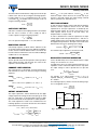
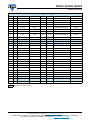
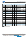
SiC401, SiC402, SiC403 www.vishay.com Vishay Siliconix Reference Board User’s Manual for SiC403 (6 A), SiC402 (10 A), and SiC401 (15 A) Synchronous Buck Regulators PRODUCT SUMMARY SiC401A, SIC401BCD Input Voltage Range 3 V to 17 V Output Voltage Range 0.6 V to VIN x 0.75 Operating Frequency 200 kHz to 1 MHz Continuous Output Current Package 15 A MLP55-32L FEATURES • SiC401A/B: 3 V to 17 V input range. SiC402A/B, SiC403A/B: 3 V to 28 V input range. • Adjustable output voltage down to 0.6 V • 6 A (SiC403), 10 A (SiC402), and 15 A (SiC401) continuous output current • Selectable frequency from 200 kHz to 1 MHz with an external resistor PRODUCT SUMMARY SiC402A, SIC402BCD Input Voltage Range 3 V to 28 V • 95 % peak efficiency Output Voltage Range 0.6 V to VIN x 0.75 • Stable with any capacitor; no external ESR network required Operating Frequency 200 kHz to 1 MHz • Ultrafast transient response Continuous Output Current Package 10 A MLP55-32L • Power saving scheme for increased light load efficiency • ± 1 % accuracy of VOUT setting • Cycle-by-cycle current limit PRODUCT SUMMARY SiC403A, SIC403BCD • Fully protected with OTP, SCP, UVP, OVP Input Voltage Range • PGOOD Indicator 3 V to 28 V Output Voltage Range 0.6 V to VIN x 0.75 Operating Frequency 200 kHz to 1 MHz Continuous Output Current Package 6A MLP55-32L • -40 °C to +125 °C operating junction temperature • Output voltage tracking APPLICATIONS Note • External divider network needed • Point of load regulation for low-power processors, network processors, DSPs, FPGAs, and ASICs DESCRIPTION • Low voltage, distributed power architectures with 5 V or 12 V, or 24 V rails The SiC401, SiC402, and SiC403 are high frequency voltage-mode constant-on-time (CM-COT) synchronous buck regulators with integrated high-side and low-side power MOSFETs. The SiC403 is capable of 6 A continuous current, the SiC402 is capable of 10 A and the SiC401 15 A. These regulators produce an adjustable output voltage which in standard setup can output 5 V down to 0.6 V and with the VOUT divider network 75 % of VIN down to 0.6 V to accommodate a variety of applications, including computing, consumer electronics, telecom, and industrial. The CM-COT architecture delivers ultra-fast transient response with minimum output capacitance and tight ripple regulation at very light load. The parts are stable with any capacitor type and no ESR network is required for loop stability. The regulator integrates a full protection feature set, it also has UVLO for the input rail and an internal soft-start. • Computing, broadband, networking, LAN / WAN, optical, test, and measurement • A / V, high density cards, storage, DSL, STB, DVR, DTV, industrial PC ORDERING INFORMATION BOARD PART NUMBER MAX. OUTPUT CURRENT SiC403DB-LC 6A SiC402DB-HC 10 A SiC401DB-HC 15 A Notes • LC - low current inductor, HC - high current inductor • The only difference between HC and LC board is the O / P inductor size The SiC40X family is available in lead (Pb)-free power enhanced 5 mm x 5 mm MLP55-32L package. Revision: 17-Nov-14 Document Number: 62923 1 For technical questions, contact: [email protected] THIS DOCUMENT IS SUBJECT TO CHANGE WITHOUT NOTICE. THE PRODUCTS DESCRIBED HEREIN AND THIS DOCUMENT ARE SUBJECT TO SPECIFIC DISCLAIMERS, SET FORTH AT www.vishay.com/doc?91000 SiC401, SiC402, SiC403 www.vishay.com Vishay Siliconix SPECIFICATIONS Output Voltage Sense This reference board allows the end user to evaluate the SiC401, SiC402, or the SiC403 chip for its features and all functionalities. VOUT_SENSE, GNDOUT_SENSE (P4): This allows the user to measure the voltage at the output of the regulator and remove any losses generated due to the connections, from the measurement. This can also be used by an active load with sense capability. It can also be a reference design for a user’s application. CONNECTION AND SIGNAL / TEST POINTS Power Sockets VIN, GND (P1): Input voltage source with VIN to be positive. Connect to a voltage source: - SiC401A/BCD - 3 V to 17 V - SiC402A/BCD - 3 V to 28 V - SiC403A/BCD - 3 V to 28 V VOUT, GND (P3): Output voltage with VOUT to be positive. Connect to a load that draws no more than: • SiC401A/BCD - 15 A • SiC402A/BCD - 10 A • SiC403A/BCD - 6 A 5 V, GND (P5): External 5 V voltage source with 5 V to be positive. Connect to a 5 V source when this option is selected. SELECTION JUMPERS Mode Select P7: This is a 2 way header which allows the user to select either power save mode or constant PWM mode. OPEN - forced PWM, the pin is floating SHORT - power save mode, the pin is at 5 V A third option is available whereby pin 2 is shorted to 0 V to disable the part. UVLO Option P8: This is a 2 way header that will enable the UVLO function when selected. The divider resistors R1 and R2 can be changed depending on the required turn on voltage level, the pin requires a voltage greater than 3 V to enable. OPEN - UVLO disabled SHORT - UVLO enabled VDD Select P6: This is a 3 way header that will enable the user to select between internal LDO and an external 5 V supply. Position 1 - SHORT PIN 1-2 - internal LDO Position 2 - SHORT PIN 2-3 - external 5 V SIGNALS AND TEST LEADS PGD (P9): Is an open drain output and is pulled up with a 10 kΩ resistor to VIN. When FB or VOUT are within -10 % to +20 % percent of the set voltage this pin will go HI to indicate the output is okay. The pin will also follow EN/PSV condition switching LO if the IC is disabled. POWER UP PROCEDURE To turn-on the reference board, apply 12 V to VIN with the P6 jumper is in Position 1. If the P7 jumper is in place the board will come up in power save mode, if not in place then constant PWM will be observed. When applying higher than 12 V to the input it is reasonable to install a RC snubber from LX to GND. There are place holders on the reference board R9 and C11 for the snubber. Values of 10 Ω and 1 nF are a reasonable starting point. ADJUSTMENTS TO THE REFERENCE BOARD OUTPUT VOLTAGE ADJUSTMENT If a different output voltage is needed, simply change the value of VOUT and solve for R12 based on the following formula: V OUT - V FB R 12 = R 13 x ----------------------------V FB Where VFB is 0.6 V for the SiC40X. CHANGING SWITCHING FREQUENCY The following equation illustrates the relationship between ON-time, VIN, VOUT, and RON value: k R tON = --------------------------------25 pF x F SW Where k equals 1 when VDD is greater than 3.6 V. When k is less than 3.6 V and VIN is greater than ((VDD - 1.75 V) x 10), k is shown by the following equation: ( V DD - 1.75 V ) x 10 k = ---------------------------------------------------V IN The maximum Rton value allowed is shown: V IN min. R tON MAX. = -----------------15 μA Input Voltage Sense VIN_SENSE, GNDIN_SENSE (P2): This allows the user to measure the voltage at the input of the regulator and remove any losses generated due to the, connections from the measurement. This can also be used by a power source with sense capability. Revision: 17-Nov-14 Document Number: 62923 2 For technical questions, contact: [email protected] THIS DOCUMENT IS SUBJECT TO CHANGE WITHOUT NOTICE. THE PRODUCTS DESCRIBED HEREIN AND THIS DOCUMENT ARE SUBJECT TO SPECIFIC DISCLAIMERS, SET FORTH AT www.vishay.com/doc?91000 SiC401, SiC402, SiC403 www.vishay.com OUTPUT RIPPLE VOLTAGE Output ripple voltage is measured with a tip and barrel measurement across COUT. Typically output ripple voltage is set to 3 % to 5 % of the output voltage, but an all ceramic output solution can bring output ripple voltage to a much lower level since the ESR of ceramics is very small. If ceramics or a combination of ceramics and bulk capacitors are used it may be necessary to add a voltage injection network. VOLTAGE INJECTION NETWORK This is the network seen placed across the output inductor in the schematic consisting of R8, C9, and C10. A quick method to add or remove injection is to reduce or increase R4. The time constant of the inductor (τIND) and voltage injection network are as follows: L τ IND = -----------DCR and τ RIN = R L x C L In (1) the recommended value of C9 = 10 nF. Vishay Siliconix Other than the inductance the DCR and saturation current parameters are key values. The DCR causes an I2R loss which will decrease the system efficiency and generate heat. The saturation current has to be higher than the maximum output current plus 1/2 the ripple current. In over current condition the inductor current may be very high. All this needs to be considered when selecting the inductor. On this board Vishay IHLP series inductors are used to meet cost requirement and high efficiency, a part that utilizes a material that has incredible saturation levels compared to competing products. OUTPUT CAPACITOR SELECTION Voltage rating, ESR, transient response, overall PCB area and cost are requirements for selecting output capacitors. The types of capacitors and there general advantages and disadvantages are covered next. Electrolytic have high ESR, dry out over time so ripple current rating must be examined and have slower transient response, but are fairly inexpensive for the amount of overall capacitance. Tantalums can come in low ESR varieties and high capacitance value for its overall size, but they fail short when damaged and also have slower transient response. The injection voltage can be checked for magnitude next using the following equation, 1 ---------V INJ = ( V IN MIN. - V OUT ) x 1 - t ---------- τ RIN e Ceramics have very low ESR, fast transient response and overall small size, but come in low capacitance values compared to the others above. A combination of technology is sensible. Where t is the ON period. This required magnitude is > 20 mVpp for stable operation, when the ripple injection voltage is smaller than 20 mVpp then double pulsing may be observed as the thresholds are not correctly triggered within the SiC40X. In order that the LDO is programmed to 5 V the divider resistors from the VDD pin to the FBL pin need to be set in order that 0.75 V is present on FBL. They can be set as follows: V DD x R 8 V LDO = -----------------------R2 + R8 The injection voltage will be DC decoupled from the FB pin via a capacitor, the calculation for this part is as follows: C 10 1 3 = --------- x -------------------------------R 12 2 x π x F SW --------R 13 LDO SETTING ENABLE PIN VOLTAGE The ENL pin will need to be set to enable the LDO. This pin accepts an input voltage up to VIN however it can also be set as an under voltage trigger. The operation for this pin can be seen in Table 1. INDUCTOR SELECTION The choice of inductor is specific to each application and quickly determined with the following equations: t ON V OUT = ------------------------------------V IN MAX. x f SW ( V IN - VOUT ) x t ON L = -------------------------------------------------I OUT MAX. x k 2 Where k2 is a percentage of maximum output current ripple required. The designer can quickly make a choice if the ripple percentage is decided, usually no more than 30 % however higher or lower percentages of IOUT can be acceptable depending on application. Revision: 17-Nov-14 TABLE 1 EN/PSV ENL LDO SWITCHER Disabled Low, < 0.4 V Off Off Enabled Low, < 0.4 V Off On Disabled 1 V < High < 2.6 V On Off Enabled 1 V < High < 2.6 V On Off Disabled High > 2.6 V On Off Enabled High > 2.6 V On On Document Number: 62923 3 For technical questions, contact: [email protected] THIS DOCUMENT IS SUBJECT TO CHANGE WITHOUT NOTICE. THE PRODUCTS DESCRIBED HEREIN AND THIS DOCUMENT ARE SUBJECT TO SPECIFIC DISCLAIMERS, SET FORTH AT www.vishay.com/doc?91000 SiC401, SiC402, SiC403 www.vishay.com The UVLO will be activated if the voltage present at this pin is below 2.6 V. This can be set using the following equation. If under voltage is not a consideration then this can be connected to VIN. The divider values for this pin can be set using the following equation: V IN x R 9 V ENL = ---------------------R1 + R9 SOFT START SETTING Soft start is a useful function helping to limit the current draw from the source at switch on. This is simply set with a ceramic capacitor using the following equation: t SS C SS = --------------------500 000 A 2. 2 nF capacitor will provide ~ 1 ms soft start time. BOOTSTRAP CIRCUIT A bootstrap capacitor of 100 nF will be sufficient for this circuit with switching frequencies from 200 kHz to 500 kHz. A series resistor has been added in order to slow down the low side switch in and minimize overshoot without adding a snubber. This is user adjustable. Vishay Siliconix Where ILPK is the peak inductor current, IMAX. is the maximum output current, dILOAD is the current step in μF and VPK is the peak voltage, the output voltage summed with the specified over and under shoot. INPUT CAPACITANCE In order to keep the design compact and minimize parasitic elements, ceramic capacitors will be chosen. The initial requirement for the input capacitance is decided by the maximum input voltage, 16 V in this case however a 35 V rated capacitor will be chosen of the X7R variety. The footprint will be a compact 1206. In order to determine the minimum capacitance the input voltage ripple needs to be specified; VCINPP ≤ 150 mV is a suitable starting point. This magnitude is determined by the final application specification. The input current needs to be determined for the lowest operating input voltage: I OUT I CIN(RMS) = ------------ x V OUT x ( V IN - V OUT ) V IN The minimum input capacitance can then be found, DC - ( 1 - DC ) C IN MIN. = I OUT x -------------------------------------V CINPP x F SW VDD DECOUPLING HIGH OUTPUT VOLTAGE OPERATION The VDD pin will need to be decoupled in order to provide a stable voltage internally and externally. The value for this capacitor is recommended as ≥ 1 μF. For the SiC40X family the recommended maximum output voltage of no more than 75 % of VIN. CURRENT LIMIT RESISTOR The current limit is set by placing a resistor between pins LXS and ILIM. The values can be found using the following equations. SiC401: R ILIM = 792 x I LIM x [ 0.101 x ( 5 V - V DD ) + 1 ] SiC402: R ILIM = 446 x I LIM x [ 0.099 x ( 5 V - V DD ) + 1 ] SiC403: R ILIM = 1176 x I LIM x [ 0.112 x ( 5 V - V DD ) + 1 ] For applications where an output voltage greater than 5 V is required a resistive network should be used to step down the output voltage in order to provide the VOUT pin with 4.5 V. R 2 x ( V OUT - V OUT PIN ) R 1 = ------------------------------------------------------------V OUT PIN For example, if an output voltage of VOUT = 8.5 V is required, setting R2 = 10 kΩ and VOUT PIN = 4.5 V results in R1 = 8870 Ω. The switching frequency will also need recalculating using a VOUT PIN magnitude of 4.5 V. V OUT PIN F SW = ------------------------t ON x V IN OUTPUT CAPACITANCE The output capacitance will be determined by the ripple voltage requirement. Voltage mode COT topology can work with very small values of capacitor ESR however a ripple injection network will also be required for stable operation. The overall capacitance needs to be calculated next. The following equations are used to calculate the size needed to meet a transient load response: I LPK = I MAX. + 0.5 x I RIPPLE MAX, C OUT MIN. = I LPK Revision: 17-Nov-14 I LPK I MAX. L x -------------- - ------------------ x dt V OUT dI LOAD x -------------------------------------------------------------2 x ( VPK - V OUT ) LX SiC40X VOUT R1 VOUT PIN COUT R2 Fig. 1 - Resistor Divider Network Allows 4.5 V at the VOUT PIN Document Number: 62923 4 For technical questions, contact: [email protected] THIS DOCUMENT IS SUBJECT TO CHANGE WITHOUT NOTICE. THE PRODUCTS DESCRIBED HEREIN AND THIS DOCUMENT ARE SUBJECT TO SPECIFIC DISCLAIMERS, SET FORTH AT www.vishay.com/doc?91000 SiC401, SiC402, SiC403 www.vishay.com Vishay Siliconix LAYOUT CONSIDERATIONS 7. If a voltage injection network is needed then place it near to the inductor LX node. The SiC40x family of footprint compatible 15 A, 10 A, and 6 A products offers the designer a scalable buck regulator solution. If the below layout recommendations are followed, the same layout can be used to cover a wide range of output currents and voltages without any changes to the board design and only minor changes to the component values in the schematic. 8. PGND can be used on internal layers if the resistance of the PCB is to be small; this will also help remove heat. Use extra vias if needed but be mindful to allow a path between the vias. The reference design has a majority of the components placed on the top layer. This allows for easy assembly and straightforward layout. 9. A quiet plane should be employed for the AGND, this is placed under the small signal passives. This can be placed on multiple layers if needed for heat removal. This should be connected to the PGND plane near to the input GND at one connection only of at least 1mm width. Figure 2 outlines the pointers for the layout considerations and the explanations follow. 10. The LX copper can also be used on multiple layers, use a number of vias. 11. The copper area beneath the inductor has been removed (on all layers) in this design to reduce the inductive coupling that occurs between the inductor and the GND trace. No other voltage planes should be placed under this area. Fig. 2 - Resistor Divider Network Allows 4.5 V at the VOUT PIN 1. Place input ceramic capacitors close to the voltage input pins with a small 10 nF / 100 nF placed as close as the design rules will allow. This will help reduce the size of the input high frequency current loop and consequently reduce the high frequency ripple noise seen at the input and the LX node. 2. Place the setup and control passive devices logically around the IC with the intention of placing a quiet ground plane beneath them on a secondary layer. 3. It is advisable to use ceramic capacitors at the output to reduce impedance. Place these as close to the IC PGND and output voltage node as design will allow. Place a small 10 nF / 100 nF ceramic capacitor closest to the IC and inductor loop. 4. The loop between LX, VOUT and the IC GND should be as compact as possible. This will lower series resistance and also make the current loop smaller enabling the high frequency response of the output capacitors to take effect. 5. The output impedance should be small when high current is required; use high current traces, multiple layers can be used with many vias. 6. Use many vias when multiple layers are involved. This will have the effect of lowering the resistance between layers and reducing the via inductance of the PCB nets. Revision: 17-Nov-14 Document Number: 62923 5 For technical questions, contact: [email protected] THIS DOCUMENT IS SUBJECT TO CHANGE WITHOUT NOTICE. THE PRODUCTS DESCRIBED HEREIN AND THIS DOCUMENT ARE SUBJECT TO SPECIFIC DISCLAIMERS, SET FORTH AT www.vishay.com/doc?91000 SiC401, SiC402, SiC403 www.vishay.com Vishay Siliconix PCB LAYOUT Revision: 17-Nov-14 Fig. 3 - Top Layer Fig. 5 - Inner Layer 2 Fig. 4 - Inner Layer 1 Fig. 6 - Bottom Layer Document Number: 62923 6 For technical questions, contact: [email protected] THIS DOCUMENT IS SUBJECT TO CHANGE WITHOUT NOTICE. THE PRODUCTS DESCRIBED HEREIN AND THIS DOCUMENT ARE SUBJECT TO SPECIFIC DISCLAIMERS, SET FORTH AT www.vishay.com/doc?91000 SiC401, SiC402, SiC403 www.vishay.com Vishay Siliconix SCHEMATIC - COMMON TO ALL BOARDS Revision: 17-Nov-14 Document Number: 62923 7 For technical questions, contact: [email protected] THIS DOCUMENT IS SUBJECT TO CHANGE WITHOUT NOTICE. THE PRODUCTS DESCRIBED HEREIN AND THIS DOCUMENT ARE SUBJECT TO SPECIFIC DISCLAIMERS, SET FORTH AT www.vishay.com/doc?91000 SiC401, SiC402, SiC403 www.vishay.com Vishay Siliconix BILL OF MATERIAL FOR SIC401 (VIN = 12 V, VOUT = 1.5 V, FSW = 500 kHz) ITEM QTY REFERENCE PCB FOOTPRINT VALUE VOLTAGE PART NUMBER MANUFACTURER 1 2 C1, C2 1206 Omit 35 V C3216X5R1V226M160AC TDK 2 2 C3, C4 1206 22 μF 35 V C3216X5R1V226M160AC TDK 3 3 C5, C9, C12 0402 10 nF 50 V GRM155R71H103KA88D Murata 4 1 C6 0402 2.2 μF 10 V C0402C225M8PACTU Kemet 5 2 C7, C10 0402 2.2 nF 50 V GRM155R71H222KA01D Murata 6 1 C8 0402 100 nF 35 V CGA2B3X7R1V104K050BB Vishay 7 5 C13, C14, C15, C16, C17 1206 47 μF 35 V GRM31CR61A476ME15L Murata 8 3 C18, C19, C20 1206 Omit 35 V GRM31CR61A476ME15L Murata 9 2 C21, C22 7343 Omit - - - 10 4 P1, P3, P9, P10 Banana Jack - - 575-4K-ND Keystone 11 5 P2, P4, P5, P7, P8 Header-2 - - 826926-2 AMP (TE) 12 1 P6 Header-3 - - HTSW-103-08-T-S Samtec 13 1 L1 IHLP5050 1 μH - IHLP5050FDER1R0 Vishay 14 1 R1 0402 249K - CRCW0402249KFKED Vishay 15 1 R2 0402 100K - CRCW0402100KFKED Vishay 16 1 R3 0402 169K - CRCW0402169KFKED Vishay 17 1 R4 0402 30K - CRCW040230K0FKED Vishay 18 1 R5 0402 5K11 - CRCW04025K11FKED Vishay 19 1 R6 0402 76K8 - CRCW040276K8FKED Vishay 20 1 R7 0402 10R - CRCW040210R0FKEA Vishay 21 1 R8 0402 10K - CRCW040210K0FKED Vishay 22 1 R9 0805 Omit - - Vishay 23 1 R10 0402 0R - CRCW04020000Z0ED Vishay 24 1 R11 0402 Omit - - Vishay 25 1 R12 0402 1K54 - CRCW04021K54FKED Vishay 26 1 R13 0402 1K - CRCW0402249KFKED Vishay 27 1 R14 0402 10R - CRCW040210R0FKEA Vishay 28 1 R15 0402 10K - CRCW040210K0FKED Vishay 29 1 U1 MLP55-33 SIC401 - - - KEY Only needed for reference board Revision: 17-Nov-14 Document Number: 62923 8 For technical questions, contact: [email protected] THIS DOCUMENT IS SUBJECT TO CHANGE WITHOUT NOTICE. THE PRODUCTS DESCRIBED HEREIN AND THIS DOCUMENT ARE SUBJECT TO SPECIFIC DISCLAIMERS, SET FORTH AT www.vishay.com/doc?91000 SiC401, SiC402, SiC403 www.vishay.com Vishay Siliconix BILL OF MATERIAL FOR SIC402 (VIN = 12 V, VOUT = 1.5 V, FSW = 500 kHz) ITEM QTY REFERENCE PCB FOOTPRINT VALUE VOLTAGE PART NUMBER MANUFACTURER 1 2 C1, C2 1206 Omit 35 V C3216X5R1V226M160AC TDK 2 2 C3, C4 1206 22 μF 35 V C3216X5R1V226M160AC TDK 3 3 C5, C9, C12 0402 10 nF 50 V GRM155R71H103KA88D Murata 4 1 C6 0402 2.2 μF 10 V C0402C225M8PACTU Kemet 5 2 C7, C10 0402 2.2 nF 50 V GRM155R71H222KA01D Murata 6 1 C8 0402 100 nF 35 V CGA2B3X7R1V104K050BB Vishay 7 3 C13, C14, C15 1206 47 μF 35 V GRM31CR61A476ME15L Murata 8 5 C16, C17, C18, C19, C20 1206 Omit 35 V GRM31CR61A476ME15L Murata 9 2 C21, C22 7343 Omit - - - 10 4 P1, P3, P9, P10 Banana Jack - - 575-4K-ND Keystone 11 5 P2, P4, P5, P7, P8 Header-2 - - 826926-2 AMP (TE) 12 1 P6 Header-3 - - HTSW-103-08-T-S Samtec 13 1 L1 IHLP4040 1 μH - IHLP4040DZER1R0 Vishay 14 1 R1 0402 249K - CRCW0402249KFKED Vishay 15 1 R2 0402 100K - CRCW0402100KFKED Vishay 16 1 R3 0402 169K - CRCW0402169KFKED Vishay 17 1 R4 0402 30K - CRCW040230K0FKED Vishay 18 1 R5 0402 5K11 - CRCW04025K11FKED Vishay 19 1 R6 0402 76K8 - CRCW040276K8FKED Vishay 20 1 R7 0402 10R - CRCW040210R0FKEA Vishay 21 1 R8 0402 10K - CRCW040210K0FKED Vishay 22 1 R9 0805 Omit - - Vishay 23 1 R10 0402 0R - CRCW04020000Z0ED Vishay 24 1 R11 0402 Omit - - Vishay 25 1 R12 0402 1K54 - CRCW04021K54FKED Vishay 26 1 R13 0402 1K - CRCW0402249KFKED Vishay 27 1 R14 0402 10R - CRCW040210R0FKEA Vishay 28 1 R15 0402 10K - CRCW040210K0FKED Vishay 29 1 U1 MLP55-33 SIC402 - - - KEY Only needed for reference board Revision: 17-Nov-14 Document Number: 62923 9 For technical questions, contact: [email protected] THIS DOCUMENT IS SUBJECT TO CHANGE WITHOUT NOTICE. THE PRODUCTS DESCRIBED HEREIN AND THIS DOCUMENT ARE SUBJECT TO SPECIFIC DISCLAIMERS, SET FORTH AT www.vishay.com/doc?91000 SiC401, SiC402, SiC403 www.vishay.com Vishay Siliconix BILL OF MATERIAL FOR SIC403 LC (VIN = 12 V, VOUT = 1.5 V, FSW = 500 kHz) ITEM QTY REFERENCE PCB FOOTPRINT VALUE VOLTAGE PART NUMBER MANUFACTURER 1 3 C1, C2, C3 1206 Omit 35 V C3216X5R1V226M160AC TDK 2 1 C4 1206 22 μF 35 V C3216X5R1V226M160AC TDK 3 3 C5, C9, C12 0402 10 nF 50 V GRM155R71H103KA88D Murata 4 1 C6 0402 2.2 μF 10 V C0402C225M8PACTU Kemet 5 2 C7, C10 0402 1 nF 50 V GRM155R71H102KA01D Murata 6 1 C8 0402 100 nF 35 V CGA2B3X7R1V104K050BB Vishay 7 2 C13, C14 1206 47 μF 35 V GRM31CR61A476ME15L Murata 8 6 C15, C16, C17 C18, C19, C20 1206 Omit 35 V GRM31CR61A476ME15L Murate 9 2 C21, C22 7343 Omit - - - 10 4 P1, P3, P9, P10 Banana Jack - - 575-4K-ND Keystone 11 5 P2, P4, P5, P7, P8 Header-2 - - 826926-2 AMP (TE) 12 1 P6 Header-3 - - HTSW-103-08-T-S Samtec 13 1 L1 IHLP3232 2.2 μH - IHLP3232DZER2R2 Vishay 14 1 R1 0402 249K - CRCW0402249KFKED Vishay 15 1 R2 0402 100K - CRCW0402100KFKED Vishay 16 1 R3 0402 169K - CRCW0402169KFKED Vishay 17 1 R4 0402 30K - CRCW040230K0FKED Vishay 18 1 R5 0402 5K11 - CRCW04025K11FKED Vishay 19 1 R6 0402 76K8 - CRCW040276K8FKED Vishay 20 1 R7 0402 10R - CRCW040210R0FKEA Vishay 21 1 R8 0402 10K - CRCW040210K0FKED Vishay 22 1 R9 0805 Omit - - Vishay 23 1 R10 0402 0R - CRCW04020000Z0ED Vishay 24 1 R11 0402 Omit - - Vishay 25 1 R12 0402 1K54 - CRCW04021K54FKED Vishay 26 1 R13 0402 1K - CRCW0402249KFKED Vishay 27 1 R14 0402 10R - CRCW040210R0FKEA Vishay 28 1 R15 0402 10K - CRCW040210K0FKED Vishay 29 1 U1 MLP55-33 SIC403 - - - KEY Only needed for reference board Vishay Siliconix maintains worldwide manufacturing capability. Products may be manufactured at one of several qualified locations. Reliability data for Silicon Technology and Package Reliability represent a composite of all qualified locations. For related documents such as package/tape drawings, part marking, and reliability data, see www.vishay.com/ppg?62923. Revision: 17-Nov-14 Document Number: 62923 10 For technical questions, contact: [email protected] THIS DOCUMENT IS SUBJECT TO CHANGE WITHOUT NOTICE. THE PRODUCTS DESCRIBED HEREIN AND THIS DOCUMENT ARE SUBJECT TO SPECIFIC DISCLAIMERS, SET FORTH AT www.vishay.com/doc?91000