1
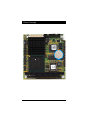
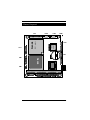
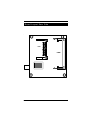
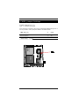
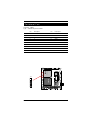
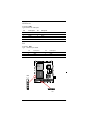
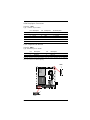
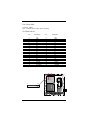
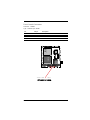
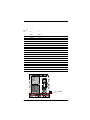
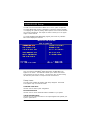
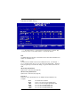
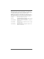
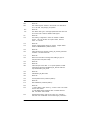
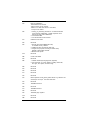
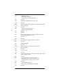
User's Manual
Version 1.0
Em104-n513
Em104-n513VL
PC/104 NS GX1 Module one SODIMM up
to 256 MB SDRAM , NS CS5530A Flat
Panel / CRT SVGA , Fast Ethernet
Introduction
Arbor's product of Em104-n513 is a PC-104 with an on-board embedded x86compatible 32 bit processors, NS Geode GX1-300 processor. With this board,
system engineers will be able to upgrade 386-based or 486-based to 586level without some additional worries, because a NS Geode GX1-300 processor is mounted on Em104-n513 and DRAM supports up to 256MB on SODIMM.
No longer worry about the CPU installation , don't need to set any jumpers of
speed or voltage of processor . And the fan is not necessary for NS Geode
Gx1-300 , the MTBF worries will be reduced . DRAM on-board will improve
the ability of the anti-vibration . Em104-n513 has the good reliability for system
designer .
With its ultra low power, rich levels of integration, advanced multimedia
capabilities and communication features, this board is an exciting opportunity
for System Integrators and OEMs to develop new generation products that
meet the desires and aspirations of the 21th century consumers.
2
Em104-n513 User's Manual
Table of Contents
Introduction ................................................................................... 2
Specifications ................................................................................ 5
Board Image .................................................................................. 7
Board Layout ................................................................................. 9
Board Layout Rear Side ............................................................. 10
Jumper/Connector Quick Reference ......................................... 11
Jumper/Connector Quick Reference ......................................... 12
CMOS Jumper Settings .............................................................. 13
Serial Port Selection (RS232C/422/485) .................................... 14
Watchdog Timer .......................................................................... 15
Fast Ethernet Connectors ........................................................... 24
Power Connector ........................................................................ 25
Interface Connectors HDD, FDD ................................................. 26
Peripheral Port ............................................................................ 28
USB Ports ..................................................................................... 29
SIR ................................................................................................ 29
VGA Displayer Connector ........................................................... 30
PS/2 Keyboard & Mouse ............................................................. 30
COM1 & COM2 for RS-232C Port ............................................... 31
Em104-n513 User's Manual
3
Compact Flash Connector .......................................................... 32
Flat Panel VGA ............................................................................ 33
Front Panel Connector ............................................................... 34
ISA PC-104 Interface ................................................................... 35
LAN Act and Link LED pin header ............................................. 37
System Resources ....................................................................... 38
AWARD BIOS Setup .................................................................... 40
Setup Items ..................................................................................................... 40
Standard CMOS Setup .................................................................................... 42
IDE HDD AUTO DETECTION .............................................................................. 44
BIOS Features Setup ...................................................................................... 46
Chipset Features Setup .................................................................................. 49
Power Management Setup .............................................................................. 51
PnP/PCI Configuration ..................................................................................... 52
Integrated Peripherals ..................................................................................... 53
POST Codes ................................................................................. 55
Howto : Flash the BIOS ............................................................... 62
What if things go wrong ............................................................. 63
Warranty ...................................................................................... 64
4
Em104-n513 User's Manual
Specifications
General Specifications
• CPU : NS Geode GX1 300MHz MHz with FSB 33MHz.
• Chipset : NS CS5530A.
• BIOS : AWARD® Flash BIOS
• Green Function : power saving supported in BIOS. DOZE / STANDBY
APM
• L1 Cache : Integrated on CPU
• DRAM Memory : up to 256MB of SDRAM on SODIMM (144-pin), Total of
256MB Memory
• Enhanced IDE with UltraDMA : supports single port and up to 2 ATAPI
devices, Ultra DMA transfer 33 MB/sec. One 44-pin (2.0 pitch) box
header.
• Watchdog Timer : 1~255 minitues generates RESET when your application loses control over the system.
• Real-time Clock : built-in chipset with lithium battery backup. CMOS data
backup of BIOS setup and BIOS default.
High Speed Multi I/O
• Chipset : Winbond 83977F-A
• Serial Ports : Two high speed RS-232C ports (COM1). One high speed
RS-232C/422/485 port COM2 (jumper selectable). Both with 16C550
compatible UART.
• USB : 2 onboard USB prots Ver 1.1.
• SIR Interface : onboard IrDA TX/RX port
• Floppy Disk Drive Interface : 2 floppy disk drives, 3.5" (720 KB, 1.44
MB or 2.88 MB).
• Bi-directional Parallel Port : SPP, EPP and ECP mode.
• Keyboard and Mouse Connectors : external PS/2 KB/Mouse port (6-pin
box header)
Em104-n513 User's Manual
5
Network Interface Controller
• Chipset : Single Realtek 8100BL, 10/100 Mbps
• Connector : Onboard 10-pin header
Display Controller
• Chipset : CS5530A, shared display memory up to 4MB
• Display Type : CRT (VGA, SVGA, XGA, SXGA) and 18-bit TFT LCD TVOut
• Connectors : Onboard 40-pin header (DF 13-40 DP-1.25V)
• Resolution: >Em104-n513/VL CRT resolutions up to 1280x1024 @ 256
colors or 1204x768 @ 16bit. Panel resolutions up to
1280x1024 @ 8bpp or 1024x768 @ 16bpp.
SSD Interfaces
• Compact Flash Card (CFC)
- Compact Flash Socket : supports Type I/II CFC
- Capacity : up to 512MB CFC
Environmental and Power
• Power Requirements : +5 V @ 0.97 A (typical);(Low Power Embedded
NS Geode GX1 300MHz and 256MB SDRAM)
•
•
•
•
6
Board Dimensions : 90mm x 96mm
Board Weight : 0.1kg
Operating Temperature : 0 to 60°C (32 to 140°F)
Operating Humidity : 0%~90%
Em104-n513 User's Manual
Board Image
Em104-n513 User's Manual
7
Warning
Single Board Computers and their components contain very
delicate Integrated Circuits (IC). To protect the Single Board
Computer and its components against damage from static
electricity, you should always follow the following precautions
when handling it :
1. Disconnect your Single Board Computer from the power source
when you want to work on the inside
2. Hold the board by the edges and try not to touch the IC chips, leads
or circuitry
3. Use a grounded wrist strap when handling computer components.
4. Place components on a grounded antistatic pad or on the bag that
came with the Single Board Computer, whenever components are
separated from the system
Ordering Codes
Em104-n513VL
PC/104 NS GX1 Module one SODIMM up to 256 MB SDRAM , NS CS5530A
Flat Panel / CRT SVGA , Fast Ethernet
8
Em104-n513 User's Manual
Board Layout
GX1- 300B-55
COM2
COM1
EKM1
LAN1
Realtek
RTL8100BL
LPT1
Geode
LCD1
IDE1
Geode
FDD1
USB1
PWR1
VGA1
SIR1
Em104-n513 User's Manual
FRONT1
J3
J2
9
Board Layout Rear Side
CFD1
DIMM1
10
Em104-n513 User's Manual
Jumper/Connector Quick Reference
Jumpers
Label
Function
J1
Clear CMOS
J2
COM2 RS-232C / 422 / 485 Selection
Em104-n513 User's Manual
11
Jumper/Connector Quick Reference
Connectors
Label
Function
VGA1
VGA Display Connector
LCD1
LCD Connector
IDE1
Primary IDE Connector
CFD1
Compact Flash Connector
USB1
USB Port 0,1
SIR1
Infrared (IR) Connector
EKM1
Keyboard and PS/2 Mouse
FDD1
Floppy Drive Connector
LAN1
10/100M LAN1 Connector
LPT1
Parallel Port
COM1
RS-232C Serial Port
COM2
RS-232C/422/485 Serial Port
PWR1
Small 4P Power Connector
PC104
ISA PC-104 Interface
FRONT1
Front Panel Connector
J3
LAN Act and Link LED pin header
DIMM1
SODIMM Socket
12
Em104-n513 User's Manual
CMOS Jumper Settings
CMOS Operation (J1)
Type : J1: onboard 3-pin header
If the Em104-n513 refuses to boot due to inappropriate CMOS settings here is
how to proceed to clear (reset) the CMOS to its default values.
J1
Status
Normal Operation
1-2
ON
Clear CMOS
default setting
2-3
ON
Realtek
GX1- 300B-55
1-2 ON
RTL8100BL
Geode
CMOS Setup (J1)
1
2
3
J1
Geode
Em104-n513 User's Manual
13
Serial Port Selection (RS232C/422/485)
RS-232C/422/485 Mode select (J2)
Type : J2: onboard 6-pin(2*3) header
J2 Selection
RS-232C
1-2
ON
3-4
OFF
5-6
OFF
RS-422
OFF
ON
OFF
RS-485
OFF
OFF
ON
default setting RS-232C
RS-422/485 Mode on COM2
The onboard COM2 port can be configured to operate in RS-422 or RS-485
modes. RS-422 modes differ in the way RX/TX is being handled. Jumper J2
switches between RS-232C or RS-422/485 mode. All of the RS-232C/422/485
modes are available on COM2.
COM2
Pin Defined:
Tx-
Data+
Pin2 :
RXD
Tx+
Data-
Pin8 :
CTS
Rx+
x
Pin9 :
RI
Rx-
x
Geode
14
RS-485
Realtek
RTL8100BL
Geode
RS-422
DCD
GX1- 300B-55
RS-232C
Pin1 :
6
4
2
5
3
1
Em104-n513 User's Manual
Watchdog Timer
Programming Example
The following program is an examples of how to enable,
disable and refresh the Watchdog timer:
;Rev
Date
Description
;---------------------------------------------------------------------------;R00
04/04/03
For W83977F-A WDT utility.
Secondio_Config_Port
Input_Loop
equ
equ
3F0h
30
.model small
.386
.code
jmp
Secondio_Early_Prg
Secondio_Early_Prg:
mov
ax,@data
mov
ds,ax
mov
es,ax
xor
ax,ax
lea
dx,topstr
mov
ah,09
Em104-n513 User's Manual
15
int
21h
lea
dx,buffer
mov
ah,0ah
int
call
lea
mov
21h
ASCII_2_HEX
dx,endstr
ah,09
int
21h
call
Secondio_Enter_Config
mov
si, offset cs:Secondio_Init_Tbl
mov
cx, Secondio_Init_Counter
Init_Secondio_Register:
push
cx
mov
cl, byte ptr cs:[si]
inc
mov
al, byte ptr cs:[si]
inc
si
call
Secondio_Set_Reg
pop
cx
loop
short Init_Secondio_Register
call
16
si
Secondio_Exit_Config
Em104-n513 User's Manual
Secondary_Prg_Super_IO_Chip:
call
Secondio_Enter_Config
Set_Watch_Dog_Timer:
mov
call
cl,8
Secondio_Set_Logic_Device
mov
al, buffer1
mov
cl, 0f2h
call
Secondio_Set_Reg
End_Secondary_Prg_Super_IO_Chip:
call
Secondio_Exit_Config
call
Show_Message
mov
int
ah,4ch
21h
Secondio_Init_Tbl:
db
02ch, 010h
db
007h, 007h
db
0e6h, 00ah
Secondio_Init_Counter
EQU
;Enable_Secondio_Support_Watch_Dog
($ - Secondio_Init_Tbl) / 2
Secondio_Enter_Config:
mov
dx, Secondio_Config_Port
mov
al, 87h
out
dx, al
Em104-n513 User's Manual
17
out
dx, al
ret
Secondio_Exit_Config:
mov
dx, Secondio_Config_Port
mov
al, 0AAh
out
dx, al
ret
Secondio_Set_Reg:
push
ax
mov
dx, Secondio_Config_Port
mov
al, cl
out
dx, al
pop
ax
inc
dx
out
dx, al
ret
Secondio_Set_Logic_Device:
mov
al, cl
mov
cl, 7
call
Secondio_Set_Reg
ret
Secondio_Set_Dev_Active:
mov
18
cl, 30h
Em104-n513 User's Manual
call
Secondio_Set_Reg
ret
Secondio_Set_Port:
mov
cl, 60h
mov
al, bh
call
Secondio_Set_Reg
mov
cl, 61h
mov
al, bl
call
Secondio_Set_Reg
ret
Secondio_Set_Irq:
mov
al, ch
mov
cl, 70h
call
Secondio_Set_Reg
ret
ASCII_2_HEX:
xor
ax,ax
mov
buffer1,al
mov
buffer2,al
mov
bx,0
mov
al,Input_Loop
inc
mov
ax
cx,ax
next:
Em104-n513 User's Manual
19
lea
si,buffer_data
lea
di,str_data[bx]
cmpsd
je
add
scan_yes
bx,8
loopne next
scan_no:
mov
al,0ffh
mov
buffer2,al
mov
al,0
mov
buffer1,al
ret
scan_yes:
dec
cl
mov
al,cl
mov
buffer1,al
lea
si,str_data[bx+4]
lea
di,wdtsecstr
movsd
ret
Show_Message:
20
mov
al,buffer2
cmp
al,0ffh
jnz
show_wdt_dis
lea
dx,errstr
mov
ah,09h
Em104-n513 User's Manual
int
jmp
21h
show_end
show_wdt_dis:
mov
al,buffer1
cmp
al,00h
jnz
show_wdt_en
lea
dx,wdtstr
mov
int
ah,09h
21h
lea
dx,wdtdis
mov
ah,09h
int
jmp
21h
show_end
show_wdt_en:
lea
mov
int
dx,wdtstr
ah,09h
21h
lea
dx,wdten
mov
ah,09h
int
21h
show_end:
lea
dx,endstr
mov
ah,09h
int
21h
ret
.stack
Em104-n513 User's Manual
21
.data
topstr
db
0ah,0dh
db
'Arbor Industrial PC-based Automation',44 dup(0)
db
buffer
'Winbond W83977F-A Superio I/O Watch Dog Timer Utility'
db
27 dup(0)
db
'Version: T1.0'
db
0ah,0dh,0ah,0dh
db
'0=Disabled,1=16sec,2=32sec,3=48......30=480sec'
db
0ah,0dh
db
'Input : ','$'
db
buffer_num
buffer_data
db
db
04h
00h
00h,00h,00h,00h,'$'
buffer1
db
00h
buffer2
db
00h
str_data
db
33h,30h,0dh,00h,' 480' ;30
22
db
32h,39h,0dh,00h,' 464' ;29
db
32h,38h,0dh,00h,' 448' ;28
db
32h,37h,0dh,00h,' 432' ;27
db
32h,36h,0dh,00h,' 416' ;26
db
32h,35h,0dh,00h,' 400' ;25
db
32h,34h,0dh,00h,' 384' ;24
db
32h,33h,0dh,00h,' 368' ;23
db
32h,32h,0dh,00h,' 352' ;22
db
32h,31h,0dh,00h,' 336' ;21
db
32h,30h,0dh,00h,' 320' ;20
db
31h,39h,0dh,00h,' 304' ;19
Em104-n513 User's Manual
db
31h,38h,0dh,00h,' 288' ;18
db
31h,37h,0dh,00h,' 272' ;17
db
31h,36h,0dh,00h,' 256' ;16
db
31h,35h,0dh,00h,' 240' ;15
db
31h,34h,0dh,00h,' 224' ;14
db
31h,33h,0dh,00h,' 208' ;13
db
31h,32h,0dh,00h,' 192' ;12
db
31h,31h,0dh,00h,' 176' ;11
db
31h,30h,0dh,00h,' 160' ;10
db
39h,0dh,00h,00h,' 144' ;9
db
38h,0dh,00h,00h,' 128' ;8
db
37h,0dh,00h,00h,' 112' ;7
db
36h,0dh,00h,00h,' 96' ;6
db
35h,0dh,00h,00h,' 80' ;5
db
34h,0dh,00h,00h,' 64' ;4
db
33h,0dh,00h,00h,' 48' ;3
db
32h,0dh,00h,00h,' 32' ;2
db
31h,0dh,00h,00h,' 16' ;1
db
30h,0dh,00h,00h,'
' ;0
wdtstr
db
0ah,0dh,'Watch Dog Timer Reset System ','$'
wdtdis
db
'Disabled','$'
wdten
db
'After'
wdtsecstr
db
'0000 '
secondstr
db
'Sec','$'
errstr
endstr
db
db
0ah,0dh,'Input Error','$'
0ah,0dh,'$'
end
Em104-n513 User's Manual
23
Fast Ethernet Connectors
10 / 100M LAN1 Connector
Connector : LAN1
Type : Onboard 10-pin header
Pin
Description
Pin
Description
1
TX+
2
TX-
3
RX+
4
NC
5
NC
6
RX-
7
NC
8
NC
9
GND
10
GND
Geode
Realtek
RTL8100BL
GX1- 300B-55
12
Geode
24
Em104-n513 User's Manual
Power Connector
Power Connector : PWR1
Connector : PWR1
Type : PWR1: onboard small 4P connector
Pin
Description
+5V
GND
2
4
GND
+12V
Realtek
RTL8100BL
Geode
Description
1
3
GX1- 300B-55
Pin
1
2
3
4
Geode
Em104-n513 User's Manual
25
Interface Connectors HDD, FDD
Floppy Disk Drive
Connector
Connector : FDD
Type : onboard 34-pin box header
Pin
Description
GND
2
RWC
3
GND
4
NC
5
GND
6
DS1
7
WDATA
8
INDEX
9
WE
10
MOA
11
TRACK0
12
DSB
13
WP
14
DSA
15
RDATA
16
MOB
17
HEAD
18
DIR
19
DSKCHG
20
STEP
Realtek
RTL8100BL
Geode
Description
1
GX1- 300B-55
Pin
12
Geode
26
Em104-n513 User's Manual
Enhanced IDE1
Connector
Connector : IDE1
Type : One onboard 44-pin box headers, primary IDE
Pin
Description
#RESET
2
GND
3
D7
4
D8
5
D6
6
D9
7
D5
8
D10
9
D4
10
D11
11
D3
12
D12
13
D2
14
D13
15
D1
16
D14
17
D0
18
D15
19
GND
20
NC
21
REQ
22
GND
23
#IOW
24
GND
25
#IOR
26
GND
27
#IORDY
28
IDESEL
29
#DACK
30
GND
31
IRQ
32
NC
33
ADDR1
34
CBLID
35
ADDR0
36
ADDR2
37
#CS0
38
#CS1(#HD SELET1)
39
#ACT
40
GND
41
Vcc
42
Vcc
43
GND
44
GND
Realtek
RTL8100BL
Geode
Description
1
GX1- 300B-55
Pin
Geode
21
Em104-n513 User's Manual
27
Peripheral Port
Connector : LPT1
Type : onboard 26-pin box header
Pin
Description
STB
2
AFD
3
PD0
4
ERR
5
1
6
INIT
7
2
8
SLIN
9
3
10
GND
11
4
12
GND
13
5
14
NC
15
6
16
BUSY
17
7
18
PE
19
ACK#
20
SLCT
Realtek
RTL8100BL
Geode
Description
1
GX1- 300B-55
Pin
12
Geode
28
Em104-n513 User's Manual
USB Ports
Connector: USB1
Type:onboard Two USB ports
Pin
Description
Pin
Description
1
VCC
2
VCC
3
DATA-
4
DATA-
5
DATA+
6
DATA+
7
GND
8
GND
9
GND
10
NC
SIR
Connector : SIR1
Type : onboard 5-pin header
Pin
Description
Vcc
IRRX
IRTX
2
4
NC
GND
Realtek
Geode
USB
RTL8100BL
Geode
Description
1
3
5
GX1- 300B-55
Pin
12
5
4
3
2
1
SIR
Em104-n513 User's Manual
29
VGA Displayer Connector
Connector : VGA1
Type : Onboard 16-pin header
Pin
Description
Pin
Description
Pin Description
1
RED
6
GND
1 1 NC
2
GREEN
7
GND
1 2 I2C-DATE
3
BLUE
8
GND
1 3 HSYNC
4
NC
9
Vcc
1 4 VSYNC
5
GND
10
GND
1 5 I2C-CLK
16
NC
PS/2 Keyboard & Mouse
Connector: KMB1
Type: Onboard 6-pin box header
Pin
Description
Pin
Description
1
3
5
KB-DATA
MS-DATA
+5V
2
4
6
GND
KB-CLK
MS-CLK
Note: KB1 supports PS/2 keyboard directly, and PS/2 mouse suppoted with the additional
PS2 1-to-2 cable in the standard packing.
KBM1
Geode
Realtek
RTL8100BL
GX1- 300B-55
1
6
Geode
1
VGA
30
2
Em104-n513 User's Manual
COM1 & COM2 for RS-232C Port
Connector : COM1 & COM2
Type : onboard 10-pin box header
COM1 for RS-232
Pin
Description
Pin
Description
1
DCD
2
RXD
3
TXD
4
DTR
5
GND
6
DSR
7
RTS
8
CTS
9
RI
10
NC
COM1 for RS-422
Pin
Description
Pin
Description
1
TX+
2
TX-
3
NC
4
NC
5
GND
6
NC
7
NC
8
RX+
9
RX-
10
NC
COM1 for RS-485
Pin
Description
Pin
Description
2
DATA-
3
NC
4
NC
5
GND
6
NC
7
NC
8
NC
9
NC
10
NC
Realtek
RTL8100BL
Geode
DATA+
GX1- 300B-55
1
1
2
COM1
1
2
COM2
Geode
Em104-n513 User's Manual
31
Compact Flash Connector
Connector : CFD1
Type : 50-pin compact flash type I/II
Pin
Description
Pin Description
Pin Description
1
GND
1 8 ADDR2
3 5 IO WRITE
2
DATA3
1 9 ADDR1
3 6 +5V
3
DATA4
2 0 ADDR0
3 7 IRQ15
4
DATA5
2 1 DATA0
3 8 +5V
5
DATA6
2 2 DATA1
3 9 CSEL
6
DATA7
2 3 DATA2
4 0 N/C
7
CS#1
2 4 N/C
4 1 IDE RESET
8
GND
2 5 GND
4 2 IO READY
9
GND
2 6 GND
4 3 N/C
10
GND
2 7 DATA11
4 4 +5V
11
GND
2 8 DATA12
4 5 DASP
12
GND
2 9 DATA13
4 6 DIAG
13
+5V
3 0 DATA14
4 7 DATA8
14
GND
3 1 DATA15
4 8 DATA9
15
GND
3 2 CS#3
4 9 DATA10
16
GND
3 3 GND
5 0 GND
17
GND
3 4 IO READ
32
Em104-n513 User's Manual
Flat Panel VGA
Connector : LCD1
Type : Onboard 40-pin header (20*2 connector)
CS5530A 18-bit
+5V
GND
+3V
VEEP
R0
R2
R4
G0
G2
G4
B0
B2
B4
NC
NC
NC
GND
FPSCLK
M
FPVDDEN
Pin
Description
2
4
6
8
10
12
14
16
18
20
22
24
26
28
30
32
34
36
38
40
+5V
GND
+3V
GND
R1
R3
R5
G1
G3
G5
B1
B3
B5
NC
NC
NC
GND
VSYNC
HSYNC
VBIASEN
2
40
Em104-n513 User's Manual
Realtek
39
Geode
1
RTL8100BL
Geode
1
3
5
7
9
11
13
15
17
19
21
23
25
27
29
31
33
35
37
39
Description
GX1- 300B-55
Pin
33
Front Panel Connector
Connector : Front1
Type : Onboard 8-pin header
Description
RES
Reset
3-4
NC
5-6
HDD
Pin-5 is "HDD+",Pin6 is "HDD-"
7-8
SPEAKER
Pin-7 is "SPEAKER+",Pin-8 is "SPEAKER-"
Realtek
RTL8100BL
Geode
Jumper
1-2
GX1- 300B-55
Pin
Geode
34
S P K
H D D
- +
- +
R E S
1
Em104-n513 User's Manual
ISA PC-104 Interface
Connector : PC104 bus
Type : Onboard 30-pin and 20-pin header
J1 / P1
Pin
A
B
1
2
IOCHCK*
D7
GND
RSTDRV
3
D6
+5V
4
D5
IRQ9
5
D4
-5V
6
D3
DRQ2
7
D2
-12V
8
D1
ENDXFR*
9
D0
+12V
10
IOCHRDY
GND/KEY
11
AEN
SMEMW*
12
A19
SMEMR*
13
A18
IOW*
14
A17
IOR*
15
A16
DACK3*
16
A15
DRQ3
17
A14
DACK1*
18
A13
DRQ1
19
A12
REFRESH*
20
A11
SYSCLK
21
A10
IRQ7
22
A9
IRQ6
23
A8
IRQ5
24
A7
IRQ4
25
A6
IRQ3
26
A5
DACK2*
27
A4
TC
28
A3
BALE
29
A2
+5V
30
A1
OSC
31
A0
GND
32
GND
GND
Em104-n513 User's Manual
35
J2 / P2
Pin
D
C
GND
MEMCS16*
IOCS16*
IRQ10
SBHE*
LA23
LA22
4
IRQ11
LS21
5
IRQ12
LS20
6
IRQ15
LS19
7
IRQ14
LS18
8
DACK0*
LA17
9
DRQ0
MEMR*
10
DACK5*
MEMW*
11
DRQ5
SD8
12
DACK6*
SD9
13
DRQ6
SD10
14
DACK7*
SD11
15
DRQ7
SD12
16
+5V
SD13
17
MASTER*
SD14
18
GND
SD15
19
GND
GND/KEY
Realtek
RTL8139DL
Geode
GND
1
2
3
GX1- 300B-55
0
Geode
PC 104 BUS
36
Em104-n513 User's Manual
LAN Act and Link LED pin header
Connector : J3
Type : Onboard 4-pin header
ACTIVELINK-
Pin
Description
2
4
ACTIVE+
LINK+
Realtek
RTL8100BL
Geode
1
3
Description
GX1- 300B-55
Pin
Geode
Em104-n513 User's Manual
37
System Resources
Interrupt Assignment
IRQ
Description
0
System Timer
1
Standard 101/103-key or Microsoft Natural Keyboard
2
Programmable Interrupt Controller
3
Communication Port (COM2)
4
Communication Port (COM1)
5
National XpressAUDIO(TM) 16-bit Sound
6
Standard Floppy Disk Controller
7
Parallel Port 1 (LPT1)
8
System CMOS/real time clock
9
Reserve
10
Realtek RTL8139/810x Family Fast Ethernet NIC
12
PS/2 Compatible Mouse Port
13
Numeric data processor
14
Primary Cx5530 Bus Master IDE Controller
15
Secondary Cx5530 Bus Master IDE Controller
I/O Address Space
Adress
Description
0000 - 000F
DMA Controller
0020 - 0021
Programmable interrup controller
0040 - 0043
System Timer
0060 - 0060
Standard 101/102-key or Microsoft Natural Keyboard
0061 - 0061
System speaker
0064 - 0064
Standard 101/102-key or Microsoft Natural Keyboard
0070 - 0071
System COM/real time clock
0087 - 0087
Direct memory access controller
0089 - 008B
Direct memory access controller
008F - 0091
Direct memory access controller
00A0 - 00A1
Programmable interrupt controller
00C0 - 00DF
Motherboard Resources
00F0 - 00FF
Nuneric data processor
0170 - 0177
Cyrix 5530 Bus Master PCI to Dual IDE Controller
38
Em104-n513 User's Manual
0170 - 0177
Seoncdary Cx5530 Bus Master IDE Controller
01F0 - 01F7
Cyrix 5530 Bus Master PCI to Dual IDE Controller
01F0 - 01F7
Primary Cx5530 Bus Master IDE Controller
0220 - 022F
National XpressAUDIO(TM) 16-bit Sound
02F8 - 02FF
Communications Port(COM2)
0330 - 0331
National XpressAUDIO(TM) 16-bit Sound
0376 - 0376
Cyrix 5530 Bus Master PCI to Dual IDE Controller
0376 - 0376
Seoncdary Cx5530 Bus Master IDE Controller
0378 - 037F
Printer Port (LPT1)
0388 - 038B
National XpressAUDIO(TM) 16-bit Sound
03F2 - 03F5
Standard Floppy Disk Controller
03F6 - 03F6
Cyrix 5530 Bus Master PCI to Dual IDE Controller
03F6 - 03F6
Primary Cx5530 Bus Master IDE Controller
03F8 - 03FF
Communications Port(C0M1)
0480 - 048F
PCI bus
04D0 - 04D1
PCI bus
0CF8 - 0CFF
PCI bus
E000 - E0FF
Realtek RTL8100BL Family Fast Ethernet NIC
F000 - F00F
Primary Cx5530 Bus Master IDE Controller
F000 - F00F
Cyrix 5530 Bus Master PCI to Dual IDE Controller
F000 - F007
Primary Cx5530 Bus Master IDE Controller
F008 - F00F
Seoncdary Cx5530 Bus Master IDE Controller
Em104-n513 User's Manual
39
AWARD BIOS Setup
The SBC uses the Award PCI/ISA BIOS ver 4.5 for the system configuration.
The Award BIOS setup program is designed to provide the maximum flexibility
in configuring the system by offering various options which could be selected
for end-user requirements. This chapter is written to assist you in the proper
usage of these features.
To access AWARD PCI/ISA BIOS Setup program, press <Del> key. The Main
Menu will be displayed at this time.
Once you enter the AwardBIOS™ CMOS Setup Utility, the Main Menu will
appear on the screen. The Main Menu allows you to select from several
setup functions and two exit choices. Use the arrow keys to select among
the items and press <Enter> to accept and enter the sub-menu.
Setup Items
The main menu includes the following main setup categories. Recall that
some systems may not include all entries.
STANDARD CMOS SETUP
Use this menu for basic system configuration.
BIOS FEATURES SETUP
Use this menu to set the Advanced Features available on your system.
CHIPSET FEATURES SETUP
Use this menu to change the values in the chipset registers and optimize your
system's performance.
40
Em104-n513 User's Manual
Power Management Setup
Use this menu to specify your settings for power management.
PnP / PCI CONFIGRATION
This entry appears if your system supports PnP / PCI.
LOAD SETUP DEFAULTS
Use this menu to load the BIOS default values that are factory settings for
optimal performance system operations. While Award has designed the
custom BIOS to maximize performance, the factory has the right to change
these defaults to meet their needs.
INTEGRATED PERIPHERALS
Use this menu to specify your settings for integrated peripherals.
PASSWORD SETTING
Use this menu to set User and Supervisor Passwords.
IDE HDD AUTO DETECTION
System will detect the HDD plugged and recognizes what type it is.
SAVE & EXIT SETUP
Save CMOS value changes to CMOS and exit setup.
EXIT WITHOUT SAVING
Abandon all CMOS value changes and exit setup.
Em104-n513 User's Manual
41
Standard CMOS Setup
↑ ↓ → ← :Move Enter:Select +/-/PU/PD:Value F10:Save ESC:Exit F1:General Help
F5:Previous Values F6:Fail-SAfe Defaults F7:Optimized Defaults
Date
The BIOS determines the day of the week from the other date information; this
field is for information only.
Time
The time format is based on the 24-hour military-time clock. For example, 1
p.m. is 13:00:00. Press the ? or ( key to move to the desired field . Press the
PgUp or PgDn key to increment the setting, or type the desired value into the
field.
IDE Primary Master/Slave
Options are in sub menu (see page 44)
IDE Secondary Master/Slave
Options are in sub menu (see page 44)
Drive A, B
Select the correct specifications for the diskette drive(s) installed in the
computer.
None :
360K ;
1.2M ;
720K ;
1.44M ;
2.88M ;
42
No diskette drive installed
5.25 in 5-1/4 inch PC-type standard drive
5.25 in 5-1/4 inch AT-type high-density drive
3.5 in 3-1/2 inch double-sided drive
3.5 in 3-1/2 inch double-sided drive
3.5 in 3-1/2 inch double-sided drive
Em104-n513 User's Manual
Video Select the type of primary video subsystem in your computer. The
BIOS usually detects the correct video type automatically. The BIOS supports
a secondary video subsystem, but you do not select it in Setup.
Halt On During the power-on self-test (POST), the computer stops if the
BIOS detects a hardware error. You can tell the BIOS to ignore certain errors
during POST and continue the boot-up process. These are the selections:
No errors
POST does not stop for any errors.
All errors
If the BIOS detects any non-fatal error, POST stops and
prompts you to take corrective action.
All, But Keyboard
POST does not stop for a keyboard error, but stops for
all other errors.
All, But Diskette
POST does not stop for diskette drive errors, but stops
for all other errors.
All, But Disk/Key
POST does not stop for a keyboard or disk error, but
stops for all other errors.
Em104-n513 User's Manual
43
IDE HDD AUTO DETECTION
CMOS SETUP UTILITY - Copyright (C) 1984-2001 Award Software
IDE Primary Master
IDE HDD Auto-Detection
Press Enter
IDE Primary Master
Access Mode
[Auto]
[Auto]
Capacity
0 MB
Cylinder
Head
Precomp
Landing Zone
Sector
0
0
0
0
0
Item Help 2001
Menu Level
↑ ↓ → ← :Move Enter:Select +/-/PU/PD:Value F10:Save ESC:Exit F1:General Help
F5:Previous Values F6:Fail-SAfe Defaults F7:Optimized Defaults
IDE HDD Auto-detection
Press Enter to auto-detect the HDD on this channel. If detection is successful, it fills the remaining fields on this menu.
IDE Primary Master
Selecting 'manual' lets you set the remaining fields on this screen. Selects
the type of fixed disk. "User Type" will let you select the number of cylinders, heads, etc. Note: PRECOMP=65535 means NONE !
Capacity
Disk drive capacity (Approximated). Note that this size is usually slightly
greater than the size of a formatted disk given by a disk checking program.
Access Mode
Normal, LBA, Large or Auto Choose the access mode for this hard disk
44
Em104-n513 User's Manual
The following options are selectable only if the 'IDE Primary Master' item is set
to 'Manual'
Cylinder
Min = 0 Max = 65535
Set the number of cylinders for this hard disk.
Head
Min = 0 Max = 255
Set the number of read/write heads
Precomp
Min = 0 Max = 65535
**** Warning: Setting a value of 65535 means no hard disk
Landing zone
Min = 0 Max = 65535
**** Warning: Setting a value of 65535 means no hard disk
Sector
Min = 0 Max = 255
Number of sectors per track
We recommend that you select Type "AUTO" for all drives. The BIOS will autodetect the hard disk drive and CD-ROM drive at the POST stage.
If your hard disk drive is a SCSI device, please select "None" for your hard
drive setting.
Em104-n513 User's Manual
45
BIOS Features Setup
↑ ↓ → ← :Move Enter:Select +/-/PU/PD:Value F10:Save ESC:Exit F1:General Help
F5:Previous Values F6:Fail-SAfe Defaults F7:Optimized Defaults
Virus Warning
Allows you to choose the VIRUS Warning feature for IDE Hard Disk boot
sector protection. If this function is enabled and someone attempt to write
data into this area, BIOS will show a warning message on screen and beep.
Enabled Activates automatically when the system boots up causing a
warning message to appear when anything attempts to access the
boot sector or hard disk partition table.
Disabled No warning message will appear when anything attempts to access
the boot sector or hard disk partition table.
CPU Internal Cache
These two categories speed up memory access. However, it depends on
CPU/chipset design. Enabled : Enable cache, Disabled : Disable cache.
Onboard LAN Boot ROM
This feature allows you to run LAN Boot function. Select "Disnabled" not to
access this function.
Boot Sequence
The BIOS attempts to load the operating system from the devices in the
sequence selected in these items. The choices are : Floppy, HDD, CDROM,
Disabled.
46
Em104-n513 User's Manual
Swap Floppy Drive
If the system has two floppy drives, you can swap the logical drive name
assignments. The choice: Enabled/Disabled.
Boot Up NumLock Status
Select power on state for NumLock. The choice: Enabled/Disabled.
Boot Up System Speed
This item will speed up the sequence of system POST .
Gate A20 Option
Select if chipset or keyboard controller should control GateA20.
Normal A pin in the keyboard controller controls GateA20
Fast
Lets chipset control GateA20
Memory Parity Check
Select Enabled, Disabled and Auto. In Auto mode, the BIOS enables memory
checking automatically when it detects the parity DRAM.
Typematic Rate Setting
Key strokes repeat at a rate determined by the keyboard controller. When
enabled, the typematic rate and typematic delay can be selected.
The choice: Enabled/Disabled.
Typematic Rate (Chars/Sec)
Sets the number of times a second to repeat a key stroke when you hold the
key down. The choice: 6, 8, 10, 12, 15, 20, 24, 30.
Typematic Delay (Msec)
Sets the delay time after the key is held down before it begins to repeat the
keystroke. The choice: 250, 500, 750, 1000.
Security Option
Select whether the password is required every time the system boots or only
when you enter setup.
System The system will not boot and access to Setup will be denied if the
correct password is not entered at the prompt.
Setup
The system will boot, but access to Setup will be denied if the
correct password is not entered at the prompt.
Note
To disable security, select PASSWORD SETTING at Main Menu and
then you will be asked to enter password. Do not type anything and
just press <Enter>, it will disable security. Once the security is
disabled, the system will boot and you can enter Setup freely.
PCI/VGA Palette Snoop
Normally this option is always Disabled! Nonstandard VGA display adapters
such as overlay cards or MPEG video cards may not show colors properly.
Em104-n513 User's Manual
47
Setting Enabled should correct this problem. If this field set Enabled, any I/O
access on the ISA bus to the VGA card's palette registers will be reflected on
the PCI bus. This will allow overlay cards to adapt to the changing palette
colors.
OS Select For DRAM > 64MB
Select the operating system that is running with greater than 64MB of RAM on
the system.The choice: Non-OS2, OS2.
Video BIOS Shadow
Enabled this copies the video BIOS from ROM to RAM. effectively enhancing
performance, and reducing the amount of upper memory available by 32KB
(the C0000~C7FFF area of memory between 640 KB and 1 MB is used).
C8000-CBFFF Shadow
Enabling any of the C8000~CBFFF segments allows components to move their
firmware into these upper memory segments. However your computer can
lock-up doing so, because some devices don't like being shadowed at those
particular 16 KB segments of upper memory.
Note - In Windows 95, double click 'Computer' within Device Manager and
select 'Memory'. This will tell you what segments (if any) are being shadowed
For DOS you can use MSD.EXE to see what segments are claimed.
CC000-CFFFF - D0000-D3FFF - D4000-D7FFF - D8000-DBFFF and
DC000-DFFFF - Same as above.
48
Em104-n513 User's Manual
Chipset Features Setup
↑ ↓ → ← :Move Enter:Select +/-/PU/PD:Value F10:Save ESC:Exit F1:General Help
F5:Previous Values F6:Fail-SAfe Defaults F7:Optimized Defaults
SDRAM CAS latency Time
It controls the time delay (in clock cycles - CLKs) that passes before the
SDRAM starts to carry out a read command after receiving it. This also
determines the number of CLKs for the completion of the first part of a burst
transfer. Thus, the lower the cycle length, the faster the transaction. However, some SDRAM cannot handle the lower cycle length and may become
unstable. So, set the SDRAM Cycle Length to 2T for optimal performance if
possible but increase it to 3T if your system becomes unstable.
SDRAM Clock Ration Div By
The function will setup the speed of DRAM .
16-bit I/O Recovery(CLK)
The recovery time is the length of time measured in CPU clocks , whick the
system will delay after the completion of an imput/output request . This delay
takes place because the CPU is operating so much faster than the input/putput
bus that the CPU must be delayed to allow for the completion of the I/O
This item allows to you to derermine the recovery time allowed for 16-bit I/O.
Choices are from 1 to 8 CPU Clocks.
Em104-n513 User's Manual
49
8-bit I/O Recovery(CLK)
This item allows to you to derermine the recovery time allowed for 8-bit I/O.
Choices are from 1 to 4 CPU Clocks.
USB Controller
If your system contains a Universal Serial Bus controller and you have a USB
peripheral, select Enabled. The next option will become available.
Multiple Monitor Support
This item lets you select the primary VGA interface.
Display status
This item lets you select the primary monitor type.
Flat Panel Resolution
This item lets you select the resolution of Flat Panel.
50
Em104-n513 User's Manual
Power Management Setup
↑ ↓ → ← :Move Enter:Select +/-/PU/PD:Value F10:Save ESC:Exit F1:General Help
F5:Previous Values F6:Fail-SAfe Defaults F7:Optimized Defaults
Power Management
Enable the item will enable the power management function.
Doze Mode
After the selected period of drive inactivity, the hard disk drive powers down
while all other devices remain active.
Standby Mode
After the selected period of system inactivity, the fixed disk drive and the
video shut off while all other devices still operate at full speed.
HDD Power Down
After the selected period of HDD inactivity, the HDD will be shut down .
Modem Use IRQ
Name the interrupt request (IRQ) assigned to the modem (if any) on your
system. Activity of the selected IRQ always awakens the system.
Throttle Duty Cycle
Em104-n513 User's Manual
51
PnP/PCI Configuration
↑ ↓ → ← :Move Enter:Select +/-/PU/PD:Value F10:Save ESC:Exit F1:General Help
F5:Previous Values F6:Fail-SAfe Defaults F7:Optimized Defaults
This section describes configuring the PCI bus system. PCI, or Personal
Computer Interconnect, is a system which allows I/O devices to operate at
speeds nearing the speed the CPU itself uses when communicating with its
own special components.
PnP OS Installed
Select Yes if the system operating environment is Plug-and-Play aware (e.g.,
Windows 95).
Resource Controlled By
The Award Plug and Play BIOS can automatically configure all the boot and
Plug-and-Play compatible devices. If you select Auto, all the interrupt request
(IRQ) and DMA assignment fields disappear, as the BIOS automatically assigns
them.
Reset Configuration Data
Normally, you leave this field Disabled. Select Enabled to reset ESCD (Extended System Configuration Date) when you exit Setup if you have installed a
new add-on and the system reconfiguration has caused such a serious
conflict that the operating system cannot boot.
52
Em104-n513 User's Manual
Integrated Peripherals
↑ ↓ → ← :Move Enter:Select +/-/PU/PD:Value F10:Save ESC:Exit F1:General Help
F5:Previous Values F6:Fail-SAfe Defaults F7:Optimized Defaults
IDE HDD Block Mode
This feature enhances disk performance by allowing multi-sector data
transfers and eliminates the interrupt handling time for each sector.
Primary/Secondary IDE Channel
Select "Enabled" to activate each on-board IDE channel separately, Select
"Disabled", if you install an add-on IDE Control card
Primary & Secondary Master/Slave PIO
These four PIO fields let you set a PIO mode (0-4) for each of four IDE
devices. When under "Auto" mode, the system automatically set the best
mode for each device
Primary & Secondary Master/Slave UDMA
When set to "Auto" mode, the system will detect if the hard drive supports
Ultra DMA mode.
KBC input clock
This item will set the frequence of Keyboard controller.
Onboad FDC Controller
Configuration options: Enabled and Disabled.Enable the Floppy Disk Controller.
The default setting is "Enabled".
Em104-n513 User's Manual
53
Onboard Serial Port 1 & 2
Select an address and corresponding interrupt for the first/second serial port.
The default value for the first serial port is "3F8/IRQ4" and the second serial
port is "2F8/IRQ3".
Onboard IR Controller
This item allows you to select UART mode. The choices: IrDA, ASKIR, Normal.
IR Address Select
This item allows you to determine which I/O address you need .
IR Mode
This item allows you to determine which mode you need (IrDA, ASKIR,
Normal).
IR Transmission delay
You can delay the transmission rate of IR for compatibility for other device by
seting this item.
IR IRQ Select
This item allows you to determine which IRQ you need .
IR DMA Select
This item allows you to determine which DMA channel you need .
Onboard Parallel Port
Select address and interrupt for the Parallel port.
Parallel Port Mode
Select an operating mode for the parallel port. Mode options are Normal, EPP,
ECP, ECP/EPP.
ECP Mode Use DMA
Select a DMA channel if parallel Mode is set as ECP, ECP/EPP.
EPP Mode Select
Select a EPP Type if parallel Port is set as EPP, ECP/EPP.
Onboard LAN
Select "Enabled" if your system contains a LAN port.
54
Em104-n513 User's Manual
POST Codes
The following codes are not displayed on the screen. They can only be
viewed on the LED display of a so called POST card. The codes are listened
in the same order as the according functions are executed at PC startup. If
you have access to a POST Card reader, you can watch the system perform
each test by the value that's displayed. If the system hangs (if there's a
problem) the last value displayed will give you a good idea where and what
went wrong, or what's bad on the system board.
CODE
DESCRIPTION OF CHECK
CFh
Test CMOS R/W functionality.
C0h
Early chipset initialization:
-Disable shadow RAM
-Disable L2 cache (socket 7 or below)
-Program basic chipset registers
C1h
Detect memory
-Auto-detection of DRAM size, type and ECC.
-Auto-detection of L2 cache (socket 7 or below)
C3h
Expand compressed BIOS code to DRAM
C5h
Call chipset hook to copy BIOS back to E000 & F000
shadow RAM.
0h1
Expand the Xgroup codes locating in physical address 1000:0
02h
Reserved
03h
Initial Superio_Early_Init switch.
04h
Reserved
05h
1. Blank out screen
2. Clear CMOS error flag
06h
Reserved
07h
1. Clear 8042 interface
2. Initialize 8042 self-test
08h
1. Test special keyboard controller for Winbond 977
series Super I/O chips.
2. Enable keyboard interface.
09h
Reserved
0Ah
1. Disable PS/2 mouse interface (optional).
2. Auto detect ports for keyboard & mouse followed by a
port & interface swap (optional).
3. Reset keyboard for Winbond 977 series Super I/O chips.
0Bh
Reserved
0Ch
Reserved
Em104-n513 User's Manual
55
0Dh
Reserved
0Eh
Test F000h segment shadow to see whether it is R/W-able or
not. If test fails, keep beeping the speaker.
0Fh
Reserved
10h
Auto detect flash type to load appropriate flash R/W codes into
the run time area in F000 for ESCD & DMI support.
11h
Reserved
12h
Use walking 1's algorithm to check out interface in CMOS
circuitry. Also set real-time clock power status, and then
check for override.
13h
Reserved
14h
Program chipset default values into chipset. Chipset default
values are MODBINable by OEM customers.
15h
Reserved
16h
Initial onboard clock generator if Early_Init_Onboard_Generator
is defined. See also POST 26h.
17h
Reserved
18h
Detect CPU information including brand, SMI type (Cyrix or
Intel) and CPU level (586 or 686).
19h
Reserved
1Ah
Reserved
1Bh
Initial interrupts vector table. If no special specified, all H/W
interrupts are directed to SPURIOUS_INT_HDLR & S/W interrupts to SPURIOUS_soft_HDLR.
1Ch
Reserved
1Dh
Initial EARLY_PM_INIT switch.
1Eh
Reserved
1Fh
Load keyboard matrix (notebook platform)
20h
Reserved
21h
HPM initialization (notebook platform)
22h
Reserved
23h
1. Check validity of RTC value: e.g. a value of 5Ah is an invalid
value for RTC minute.
2. Load CMOS settings into BIOS stack. If CMOS checksum
fails, use default value instead.
24h
Prepare BIOS resource map for PCI & PnP use. If ESCD is
valid, take into consideration of the ESCD's legacy information.
56
Em104-n513 User's Manual
25h
Early PCI Initialization:
-Enumerate PCI bus number.
-Assign memory & I/O resource
-Search for a valid VGA device & VGA BIOS,
and put it into C000:0
26h
1. If Early_Init_Onboard_Generator is not defined Onboard
clock generator initialization. Disable respective clock
resource to empty PCI & DIMM slots.
2. Init onboard PWM
3. Init onboard H/W monitor devices
27h
Initialize INT 09 buffer
28h
Reserved
29h
1. Program CPU internal MTRR (P6 & PII)
for 0-640K memory address.
2. Initialize the APIC for Pentium class CPU.
3. Program early chipset according to CMOS setup.
Example: onboard IDE controller.
4. Measure CPU speed.
2Ah
Reserved
2Bh
Invoke Video BIOS
2Ch
Reserved
2Dh
1. Initialize double-byte language font (Optional)
2. Put information on screen display, including Award title,
CPU type, CPU speed, full screen logo.
2Eh
Reserved
2Fh
Reserved
30h
Reserved
31h
Reserved
32h
Reserved
33h
Reset keyboard if Early_Reset_KB is defined e.g. Winbond 977
series Super I/O chips. See also POST 63h.
34h
Reserved
35h
Test DMA Channel 0
36h
Reserved
37h
Test DMA Channel 1.
38h
Reserved
39h
Test DMA page registers.
3Ah
Reserved
3Bh
Reserved
Em104-n513 User's Manual
57
3Ch
Test 8254
3Dh
Reserved
3Eh
Test 8259 interrupt mask bits for channel 1.
3Fh
Reserved
40h
Test 8259 interrupt mask bits for channel 2.
41h
Reserved
42h
Reserved
43h
Test 8259 functionality.
44h
Reserved
45h
Reserved
46h
Reserved
47h
Initialize EISA slot
48h
Reserved
49h
1. Calculate total memory by testing the last double
word of each 64K page.
2. Program write allocation for AMD K5 CPU.
4Ah
Reserved
4Bh
Reserved
4Ch
Reserved
4Dh
Reserved
4Eh
1. Program MTRR of M1 CPU
2. Initialize L2 cache for P6 class CPU & program
CPU with proper cacheable range.
3. Initialize the APIC for P6 class CPU.
4. On MP platform, adjust the cacheable range to smaller
one in case the cacheable ranges between each CPU
are not identical.
4Fh
Reserved
50h
Initialize USB Keyboard & Mouse.
51h
Reserved
52h
Test all memory (clear all extended memory to 0)
53h
Clear password according to H/W jumper (Optional)
54h
Reserved
55h
Display number of processors (multi-processor platform)
56h
Reserved
58
Em104-n513 User's Manual
57h
1. Display PnP logo
2. Early ISA PnP initialization
-Assign CSN to every ISA PnP device.
58h
Reserved
59h
Initialize the combined Trend Anti-Virus code.
5Ah
Reserved
5Bh
(Optional Feature) Show message for entering AWDFLASH.EXE
from FDD (optional)
5Ch
Reserved
5Dh
1. Initialize Init_Onboard_Super_IO
2. Initialize Init_Onbaord_AUDIO.
5Eh
Reserved
5Fh
Reserved
60h
Okay to enter Setup utility; i.e. not until this POST stage can
users enter the CMOS setup utility.
61h
Reserved
62h
Reserved
63h
Reset keyboard if Early_Reset_KB is not defined.
64h
Reserved
65h
Initialize PS/2 Mouse
66h
Reserved
67h
Prepare memory size information for function call:
INT 15h ax=E820h
68h
Reserved
69h
Turn on L2 cache
6Ah
Reserved
6Bh
Program chipset registers according to items described in Setup
& Auto-configuration table.
6Ch
Reserved
6Dh
1. Assign resources to all ISA PnP devices.
2. Auto assign ports to onboard COM ports if the
corresponding item in Setup is set to "AUTO".
6Eh
Reserved
6Fh
1. Initialize floppy controller
2. Set up floppy related fields in 40:hardware.
70h
Reserved
Em104-n513 User's Manual
59
71h
Reserved
72h
Reserved
73h
(Reserved
74h
Reserved
75h
Detect & install all IDE devices: HDD, LS120, ZIP, CDROM? .
76h
(Optional Feature)
Enter AWDFLASH.EXE if:
-AWDFLASH.EXE is found in floppy drive.
-ALT+F2 is pressed.
77h
Detect serial ports & parallel ports.
78h
Reserved
79h
Reserved
7Ah
Detect & install co-processor
7Bh
Reserved
7Ch
Init HDD write protect.
7Dh
Reserved
7Eh
Reserved
7Fh
Switch back to text mode if full screen logo is supported.
- If errors occur, report errors & wait for keys
- If no errors occur or F1 key is pressed to continue :
wClear EPA or customization logo.
80h
Reserved
81h
Reserved
E8POST.ASM starts
82h
1. Call chipset power management hook.
2. Recover the text fond used by EPA logo
(not for full screen logo)
3. If password is set, ask for password.
83h
Save all data in stack back to CMOS
84h
Initialize ISA PnP boot devices
85h
1. USB final Initialization
2. Switch screen back to text mode
86h
Reserved
87h
NET PC: Build SYSID Structure.
88h
Reserved
60
Em104-n513 User's Manual
89h
1. Assign IRQs to PCI devices
2. Set up ACPI table at top of the memory.
8Ah
Reserved
8Bh
1. Invoke all ISA adapter ROMs
2. Invoke all PCI ROMs (except VGA)
8Ch
Reserved
8Dh
1. Enable/Disable Parity Check according to CMOS setup
2. APM Initialization
8Eh
Reserved
8Fh
Clear noise of IRQs
90h
Reserved
91h
Reserved
92h
Reserved
93h
Read HDD boot sector information for Trend Anti-Virus code
94h
1.
2.
3.
4.
5.
6.
7.
8.
95h
Update keyboard LED & typematic rate
96h
1.
2.
3.
4.
5.
FFh
Boot attempt (INT 19h)
Enable L2 cache
Program Daylight Saving
Program boot up speed
Chipset final initialization.
Power management final initialization
Clear screen & display summary table
Program K6 write allocation
Program P6 class write combining
Build MP table
Build & update ESCD
Set CMOS century to 20h or 19h
Load CMOS time into DOS timer tick
Build MSIRQ routing table.
Em104-n513 User's Manual
61
Howto : Flash the BIOS
To flash your BIOS you'll need
1) a xxxxx.bin file that is a file image of the new BIOS
2) AWDFLASH.EXE a utility that can write the data-file into the BIOS chip.
Create a new, clean DOS 6 bootable floppy with "format a: /s".
Copy flash utility and the BIOS image file to this disk.
Turn your computer off. Insert the floppy you just created and boot the
computer. As it boots up, hit the [DEL] key to enter the CMOS setup. Go to
"LOAD SETUP (or BIOS) DEFAULTS," and then save and exit the setup
program. Continue to boot with the floppy disk.
Type "AWDFLASH" to execute the flash utility. When prompted, enter the name
of the new BIOS image and begin the flash procedure. Note: If you reboot
now, you may not be able to boot again.
After the flash utility is complete, reboot the system.
What to do when the Award flasher says:
Insufficient memory
1. In CMOS Chipset Features Setup, Disable Video Bios Cacheable.
2. Hit Esc, F10, Save and exit.
3. Flash the BIOS and reboot
4. Enter CMOS Chipset Features Setup,and Enable Video Bios Cacheable,
hit Esc, F10, Save and reboot.
62
Em104-n513 User's Manual
What if things go wrong
if you use the wrong Flash BIOS or if the writing process gets interrupted,
there is a fat chance that your computer won't boot anymore.
How can you recover a corrupt BIOS ?
Boot-block booting (this works only for Award BIOS)
Modern motherboards based on Award BIOS have a boot-block BIOS. This is
small area of the BIOS that doesn't get overwritten when you flash a BIOS.
The boot-block BIOS only has support for the floppy drive. If you have the
AGP video enabled you won't see anything on the screen because the bootblock BIOS only supports an ISA videocard.
If you do not want to change your AGP video setting than proceed as
follows:
The boot-block BIOS will execute an AUTOEXEC.BAT file on a bootable
diskette. Copy an Award flasher & the correct BIOS *.bin file on the floppy
and execute it automatically by putting awdflash *.bin in the AUTOEXEC.BAT
file.
Solution 2:
Hot-swapping
1. Replace the corrupt chip by a working one. The working BIOS doesn't have
to be written for your board, it just has to give you a chance of booting to
DOS.
BIOSs for the same chipset mostly work. (Chipsets that not differ too much
also mostly work. (e.g. Triton FX chipset and Triton HX chipset)
2. Boot the system to DOS (with floppy or HD)
3. Be sure that the System BIOS cacheable option in your BIOS is enabled! If
so replace (while the computer is powered on) the BIOS chip with the corrupt
one. This should work fine with most boards because the BIOS is shadowed
in RAM.
4. Flash an appropriate BIOS to the corrupt chip and reboot.
NOTE: Use a flasher from MRBIOS (http://www.mrbios.com). Utilities that
come with your motherboard often use specific BIOS-hooks. Because you
have booted with a BIOS not written for your motherboard they usually don't
work. The MR Flash utilities communicate directly with your Flash Rom and
always work. In most cases they flash a non-MRBIOS to your BIOS chip
without problems.
Em104-n513 User's Manual
63
Warranty
This product is warranted to be in good working order for a period of two
years from the date of purchase. Should this product fail to be in good
working order at any time during this period, we will, at our option, replace or
repair it at no additional charge except as set forth in the following terms.
This warranty does not apply to products damaged by misuse, modifications,
accident or disaster.
Vendor assumes no liability for any damages, lost profits, lost savings or any
other incidental or consequential damage resulting from the use, misuse of, or
inability to use this product. Vendor will not be liable for any claim made by
any other related party.
Return authorization must be obtained from the vendor before returned
merchandise will be accepted. Authorization can be obtained by calling or
faxing the vendor and requesting a Return Merchandise Authorization (RMA)
number. Returned goods should always be accompanied by a clear problem
description.
64
Em104-n513 User's Manual