1
Chapter 26
ADC12
The ADC12 module is a high-performance 12-bit analog-to-digital converter
(ADC). This chapter describes the ADC12. The ADC12 is implemented in the
MSP430x43x MSP430x44x, and MSP430FG461x devices.
Topic
Page
26.1 ADC12 Introduction . . . . . . . . . . . . . . . . . . . . . . . . . . . . . . . . . . . . . . . . . . 26-2
26.2 ADC12 Operation . . . . . . . . . . . . . . . . . . . . . . . . . . . . . . . . . . . . . . . . . . . . 26-4
26.3 ADC12 Registers . . . . . . . . . . . . . . . . . . . . . . . . . . . . . . . . . . . . . . . . . . . . 26-20
ADC12
26-1
ADC12 Introduction
26.1 ADC12 Introduction
The ADC12 module supports fast, 12-bit analog-to-digital conversions. The
module implements a 12-bit SAR core, sample select control, reference
generator and a 16 word conversion-and-control buffer. The
conversion-and-control buffer allows up to 16 independent ADC samples to be
converted and stored without any CPU intervention.
ADC12 features include:
- Greater than 200-ksps maximum conversion rate
- Monotonic 12-bit converter with no missing codes
- Sample-and-hold with programmable sampling periods controlled by
software or timers.
- Conversion initiation by software, Timer_A, or Timer_B
- Software selectable on-chip reference voltage generation (1.5 V or 2.5 V)
- Software selectable internal or external reference
- Eight individually configurable external input channels (twelve on
MSP430FG43x and MSP430FG461x devices)
- Conversion channels for internal temperature sensor, AVCC, and external
references
- Independent channel-selectable reference sources for both positive and
negative references
- Selectable conversion clock source
- Single-channel, repeat-single-channel, sequence, and repeat-sequence
conversion modes
- ADC core and reference voltage can be powered down separately
- Interrupt vector register for fast decoding of 18 ADC interrupts
- 16 conversion-result storage registers
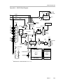
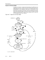
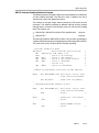
The block diagram of ADC12 is shown in Figure 26−1.
26-2
ADC12
ADC12 Introduction
Figure 26−1. ADC12 Block Diagram
REFON
INCHx=0Ah
REF2_5V
Ve REF+
on
1.5 V or 2.5 V
Reference
VREF+
VREF− / Ve REF−
AVCC
INCHx
AVSS
4
A0
A1
A2
A3
A4
A5
A6
A7
0000
0001
0010
0011
0100
0101
0110
0111
1000
1001
1010
1011
1100
1101
1110
1111
A12†
A13†
A14†
A15†
SREF2
1
Ref_x
SREF1
SREF0
11 10 01 00
ADC12OSC
ADC12SSELx
ADC12ON
0
AVCC
ADC12DIVx
VR−
Sample
and
Hold
VR+
00
Divider
/1 .. /8
12−bit SAR
Convert
S/H
ADC12CLK
01
ACLK
10
MCLK
11
SMCLK
BUSY
SHP
SHSx
ISSH
SHT0x
ENC
4
1
SAMPCON
AVCC
Sample Timer
/4 .. /1024
0
SHI
0
1
Sync
4
SHT1x
00
ADC12SC
01
TA1
10
TB0
11
TB1
MSC
INCHx=0Bh
Ref_x
R
R
CSTARTADDx
CONSEQx
AVSS
†
ADC12MEM0
ADC12MCTL0
−
16 x 12
Memory
Buffer
−
−
16 x 8
Memory
Control
−
ADC12MEM15
ADC12MCTL15
MSP430FG43x and MSP430FG461x devices only
ADC12
26-3
ADC12 Operation
26.2 ADC12 Operation
The ADC12 module is configured with user software. The setup and operation
of the ADC12 is discussed in the following sections.
26.2.1 12-Bit ADC Core
The ADC core converts an analog input to its 12-bit digital representation and
stores the result in conversion memory. The core uses two
programmable/selectable voltage levels (VR+ and VR−) to define the upper and
lower limits of the conversion. The digital output (NADC) is full scale (0FFFh)
when the input signal is equal to or higher than VR+, and zero when the input
signal is equal to or lower than VR−. The input channel and the reference
voltage levels (VR+ and VR−) are defined in the conversion-control memory.
The conversion formula for the ADC result NADC is:
N ADC + 4095
Vin * V R*
V R) * V R*
The ADC12 core is configured by two control registers, ADC12CTL0 and
ADC12CTL1. The core is enabled with the ADC12ON bit. The ADC12 can be
turned off when not in use to save power. With few exceptions the ADC12
control bits can only be modified when ENC = 0. ENC must be set to 1 before
any conversion can take place.
Conversion Clock Selection
The ADC12CLK is used both as the conversion clock and to generate the
sampling period when the pulse sampling mode is selected. The ADC12
source clock is selected using the ADC12SSELx bits and can be divided by
1 to 8 using the ADC12DIVx bits. Possible ADC12CLK sources are SMCLK,
MCLK, ACLK, and an internal oscillator, ADC12OSC.
The ADC12OSC, generated internally, is in the 5-MHz range but varies with
individual devices, supply voltage, and temperature. See the device-specific
data sheet for the ADC12OSC specification.
The user must ensure that the clock chosen for ADC12CLK remains active
until the end of a conversion. If the clock is removed during a conversion, the
operation will not complete and any result will be invalid.
26-4
ADC12
ADC12 Operation
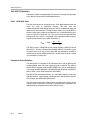
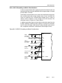
26.2.2 ADC12 Inputs and Multiplexer
The eight external and four internal analog signals are selected as the channel
for conversion by the analog input multiplexer. The input multiplexer is a
break-before-make type to reduce input-to-input noise injection resulting from
channel switching as shown in Figure 26−2. The input multiplexer is also a
T-switch to minimize the coupling between channels. Channels that are not
selected are isolated from the A/D and the intermediate node is connected to
analog ground (AVSS) so that the stray capacitance is grounded to help
eliminate crosstalk.
The ADC12 uses the charge redistribution method. When the inputs are
internally switched, the switching action may cause transients on the input
signal. These transients decay and settle before causing errant conversion.
Figure 26−2. Analog Multiplexer
R ~ 100 Ohm
ADC12MCTLx.0−3
Input
Ax
ESD Protection
Analog Port Selection
The ADC12 inputs are multiplexed with the port P6 pins, which are digital
CMOS gates. When analog signals are applied to digital CMOS gates,
parasitic current can flow from VCC to GND. This parasitic current occurs if the
input voltage is near the transition level of the gate. Disabling the port pin buffer
eliminates the parasitic current flow and therefore reduces overall current
consumption. The P6SELx bits provide the ability to disable the port pin input
and output buffers.
; P6.0 and P6.1 configured for analog input
BIS.B #3h,&P6SEL
; P6.1 and P6.0 ADC12 function
ADC12
26-5
ADC12 Operation
26.2.3 Voltage Reference Generator
The ADC12 module contains a built-in voltage reference with two selectable
voltage levels, 1.5 V and 2.5 V. Either of these reference voltages may be used
internally and externally on pin VREF+.
Setting REFON=1 enables the internal reference. When REF2_5V = 1, the
internal reference is 2.5 V, the reference is 1.5 V when REF2_5V = 0. The
reference can be turned off to save power when not in use.
For proper operation the internal voltage reference generator must be
supplied with storage capacitance across VREF+ and AVSS. The recommended
storage capacitance is a parallel combination of 10-μF and 0.1-μF capacitors.
From turn-on, a maximum of 17 ms must be allowed for the voltage reference
generator to bias the recommended storage capacitors. If the internal
reference generator is not used for the conversion, the storage capacitors are
not required.
Note: Reference Decoupling
Approximately 200 μA is required from any reference used by the ADC12
while the two LSBs are being resolved during a conversion. A parallel
combination of 10-μF and 0.1-μF capacitors is recommended for any
reference used as shown in Figure 26−11.
External references may be supplied for VR+ and VR− through pins VeREF+ and
VREF−/VeREF− respectively.
26.2.4 Auto Power-Down
The ADC12 is designed for low power applications. When the ADC12 is not
actively converting, the core is automatically disabled and automatically
re-enabled when needed. The ADC12OSC is also automatically enabled
when needed and disabled when not needed. The reference is not
automatically disabled, but can be disabled by setting REFON = 0. When the
core, oscillator, or reference are disabled, they consume no current.
26-6
ADC12
ADC12 Operation
26.2.5 Sample and Conversion Timing
An analog-to-digital conversion is initiated with a rising edge of the sample
input signal SHI. The source for SHI is selected with the SHSx bits and
includes the following:
-
The ADC12SC bit
The Timer_A Output Unit 1
The Timer_B Output Unit 0
The Timer_B Output Unit 1
The polarity of the SHI signal source can be inverted with the ISSH bit. The
SAMPCON signal controls the sample period and start of conversion. When
SAMPCON is high, sampling is active. The high-to-low SAMPCON transition
starts the analog-to-digital conversion, which requires 13 ADC12CLK cycles.
Two different sample-timing methods are defined by control bit SHP, extended
sample mode and pulse mode.
Extended Sample Mode
The extended sample mode is selected when SHP = 0. The SHI signal directly
controls SAMPCON and defines the length of the sample period tsample. When
SAMPCON is high, sampling is active. The high-to-low SAMPCON transition
starts the conversion after synchronization with ADC12CLK. See Figure 26−3.
Figure 26−3. Extended Sample Mode
Start
Sampling
Stop
Sampling
Start
Conversion
Conversion
Complete
SHI
13 x ADC12CLK
SAMPCON
tsample
tconvert
t sync
ADC12CLK
ADC12
26-7
ADC12 Operation
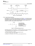
Pulse Sample Mode
The pulse sample mode is selected when SHP = 1. The SHI signal is used to
trigger the sampling timer. The SHT0x and SHT1x bits in ADC12CTL0 control
the interval of the sampling timer that defines the SAMPCON sample period
tsample. The sampling timer keeps SAMPCON high after synchronization with
AD12CLK for a programmed interval tsample. The total sampling time is tsample
plus tsync. See Figure 26−4.
The SHTx bits select the sampling time in 4x multiples of ADC12CLK. SHT0x
selects the sampling time for ADC12MCTL0 to 7 and SHT1x selects the
sampling time for ADC12MCTL8 to 15.
Figure 26−4. Pulse Sample Mode
Start
Sampling
Stop
Sampling
Conversion
Complete
Start
Conversion
SHI
13 x ADC12CLK
SAMPCON
tsample
tsync
ADC12CLK
26-8
ADC12
tconvert
ADC12 Operation
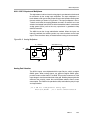
Sample Timing Considerations
When SAMPCON = 0 all Ax inputs are high impedance. When SAMPCON = 1,
the selected Ax input can be modeled as an RC low-pass filter during the
sampling time tsample, as shown below in Figure 26−5. An internal MUX-on
input resistance RI (maximum 2 kΩ) in series with capacitor CI (maximum
40 pF) is seen by the source. The capacitor CI voltage VC must be charged to
within 1/2 LSB of the source voltage VS for an accurate 12-bit conversion.
Figure 26−5. Analog Input Equivalent Circuit
MSP430
RS
VS
RI
VI
VC
CI
VI = Input voltage at pin Ax
VS = External source voltage
RS = External source resistance
RI = Internal MUX-on input resistance
CI = Input capacitance
VC = Capacitance-charging voltage
The resistance of the source RS and RI affect tsample. The following equation
can be used to calculate the minimum sampling time tsample for a 12-bit
conversion:
t
sample
u (R S ) R I)
ln(2 13)
C I ) 800ns
Substituting the values for RI and CI given above, the equation becomes:
t
sample
u (R S ) 2k)
9.011
40pF ) 800ns
For example, if RS is 10 kΩ, tsample must be greater than 5.13 μs.
ADC12
26-9
ADC12 Operation
26.2.6 Conversion Memory
There are 16 ADC12MEMx conversion memory registers to store conversion
results. Each ADC12MEMx is configured with an associated ADC12MCTLx
control register. The SREFx bits define the voltage reference and the INCHx
bits select the input channel. The EOS bit defines the end of sequence when
a sequential conversion mode is used. A sequence rolls over from
ADC12MEM15 to ADC12MEM0 when the EOS bit in ADC12MCTL15 is not
set.
The CSTARTADDx bits define the first ADC12MCTLx used for any
conversion. If the conversion mode is single-channel or repeat-single-channel
the CSTARTADDx points to the single ADC12MCTLx to be used.
If the conversion mode selected is either sequence-of-channels or
repeat-sequence-of-channels, CSTARTADDx points to the first
ADC12MCTLx location to be used in a sequence. A pointer, not visible to
software, is incremented automatically to the next ADC12MCTLx in a
sequence when each conversion completes. The sequence continues until an
EOS bit in ADC12MCTLx is processed - this is the last control byte processed.
When conversion results are written to a selected ADC12MEMx, the
corresponding flag in the ADC12IFGx register is set.
26.2.7 ADC12 Conversion Modes
The ADC12 has four operating modes selected by the CONSEQx bits as
discussed in Table 26−1.
Table 26−1.Conversion Mode Summary
CONSEQx
26-10
ADC12
Mode
Operation
00
Single channel
single-conversion
A single channel is converted once.
01
Sequence-ofchannels
A sequence of channels is converted once.
10
Repeat-singlechannel
A single channel is converted repeatedly.
11
Repeat-sequenceof-channels
A sequence of channels is converted
repeatedly.
ADC12 Operation
Single-Channel Single-Conversion Mode
A single channel is sampled and converted once. The ADC result is written to
the ADC12MEMx defined by the CSTARTADDx bits. Figure 26−6 shows the
flow of the Single-Channel, Single-Conversion mode. When ADC12SC
triggers a conversion, successive conversions can be triggered by the
ADC12SC bit. When any other trigger source is used, ENC must be toggled
between each conversion.
Figure 26−6. Single-Channel, Single-Conversion Mode
CONSEQx = 00
ADC12
off
ADC12ON = 1
ENC =
x = CSTARTADDx
Wait for Enable
ENC =
SHSx = 0
and
ENC = 1 or
and
ADC12SC =
ENC =
Wait for Trigger
SAMPCON =
ENC = 0
SAMPCON = 1
ENC = 0†
Sample, Input
Channel Defined in
ADC12MCTLx
SAMPCON =
12 x ADC12CLK
Convert
ENC = 0†
1 x ADC12CLK
Conversion
Completed,
Result Stored Into
ADC12MEMx,
ADC12IFG.x is Set
x = pointer to ADC12MCTLx
†Conversion result is unpredictable
ADC12
26-11
ADC12 Operation
Sequence-of-Channels Mode
A sequence of channels is sampled and converted once. The ADC results are
written to the conversion memories starting with the ADCMEMx defined by the
CSTARTADDx bits. The sequence stops after the measurement of the
channel with a set EOS bit. Figure 26−7 shows the sequence-of-channels
mode. When ADC12SC triggers a sequence, successive sequences can be
triggered by the ADC12SC bit. When any other trigger source is used, ENC
must be toggled between each sequence.
Figure 26−7. Sequence-of-Channels Mode
CONSEQx = 01
ADC12
off
ADC12ON = 1
ENC =
x = CSTARTADDx
Wait for Enable
ENC =
SHSx = 0
and
ENC = 1 or
and
ADC12SC =
ENC =
Wait for Trigger
EOS.x = 1
SAMPCON =
SAMPCON = 1
If x < 15 then x = x + 1
else x = 0
Sample, Input
Channel Defined in
ADC12MCTLx
If x < 15 then x = x + 1
else x = 0
SAMPCON =
MSC = 1
and
SHP = 1
and
EOS.x = 0
12 x ADC12CLK
Convert
1 x ADC12CLK
Conversion
Completed,
Result Stored Into
ADC12MEMx,
ADC12IFG.x is Set
x = pointer to ADC12MCTLx
26-12
ADC12
(MSC = 0
or
SHP = 0)
and
EOS.x = 0
ADC12 Operation
Repeat-Single-Channel Mode
A single channel is sampled and converted continuously. The ADC results are
written to the ADC12MEMx defined by the CSTARTADDx bits. It is necessary
to read the result after the completed conversion because only one
ADC12MEMx memory is used and is overwritten by the next conversion.
Figure 26−8 shows repeat-single-channel mode
Figure 26−8. Repeat-Single-Channel Mode
CONSEQx = 10
ADC12
off
ADC12ON = 1
ENC =
x = CSTARTADDx
Wait for Enable
ENC =
SHSx = 0
and
ENC = 1 or
and
ADC12SC =
ENC =
Wait for Trigger
ENC = 0
SAMPCON =
SAMPCON = 1
Sample, Input
Channel Defined in
ADC12MCTLx
SAMPCON =
12 x ADC12CLK
MSC = 1
and
SHP = 1
and
ENC = 1
Convert
1 x ADC12CLK
(MSC = 0
or
SHP = 0)
and
ENC = 1
Conversion
Completed,
Result Stored Into
ADC12MEMx,
ADC12IFG.x is Set
x = pointer to ADC12MCTLx
ADC12
26-13
ADC12 Operation
Repeat-Sequence-of-Channels Mode
A sequence of channels is sampled and converted repeatedly. The ADC
results are written to the conversion memories starting with the ADC12MEMx
defined by the CSTARTADDx bits. The sequence ends after the measurement
of the channel with a set EOS bit and the next trigger signal re-starts the
sequence. Figure 26−9 shows the repeat-sequence-of-channels mode.
Figure 26−9. Repeat-Sequence-of-Channels Mode
CONSEQx = 11
ADC12
off
ADC12ON = 1
ENC =
x = CSTARTADDx
Wait for Enable
ENC =
SHSx = 0
and
ENC = 1 or
and
ADC12SC =
ENC =
Wait for Trigger
ENC = 0
and
EOS.x = 1
SAMPCON =
SAMPCON = 1
Sample, Input
Channel Defined in
ADC12MCTLx
SAMPCON =
If EOS.x = 1 then
x = CSTARTADDx
else {if x < 15 then x = x + 1 else
x = 0}
MSC = 1
and
SHP = 1
and
(ENC = 1
or
EOS.x = 0)
x = pointer to ADC12MCTLx
26-14
ADC12
If EOS.x = 1 then
x = CSTARTADDx
else {if x < 15 then x = x + 1 else
x = 0}
12 x ADC12CLK
Convert
1 x ADC12CLK
Conversion
Completed,
Result Stored Into
ADC12MEMx,
ADC12IFG.x is Set
(MSC = 0
or
SHP = 0)
and
(ENC = 1
or
EOS.x = 0)
ADC12 Operation
Using the Multiple Sample and Convert (MSC) Bit
To configure the converter to perform successive conversions automatically
and as quickly as possible, a multiple sample and convert function is available.
When MSC = 1, CONSEQx > 0, and the sample timer is used, the first rising
edge of the SHI signal triggers the first conversion. Successive conversions
are triggered automatically as soon as the prior conversion is completed.
Additional rising edges on SHI are ignored until the sequence is completed in
the single-sequence mode or until the ENC bit is toggled in
repeat-single-channel, or repeated-sequence modes. The function of the ENC
bit is unchanged when using the MSC bit.
Stopping Conversions
Stopping ADC12 activity depends on the mode of operation. The
recommended ways to stop an active conversion or conversion sequence are:
- Resetting ENC in single-channel single-conversion mode stops a
conversion immediately and the results are unpredictable. For correct
results, poll the busy bit until reset before clearing ENC.
- Resetting ENC during repeat-single-channel operation stops the
converter at the end of the current conversion.
- Resetting ENC during a sequence or repeat-sequence mode stops the
converter at the end of the sequence.
- Any conversion mode may be stopped immediately by setting the
CONSEQx = 0 and resetting ENC bit. Conversion data are unreliable.
Note: No EOS Bit Set For Sequence
If no EOS bit is set and a sequence mode is selected, resetting the ENC bit
does not stop the sequence. To stop the sequence, first select a
single-channel mode and then reset ENC.
ADC12
26-15
ADC12 Operation
26.2.8 Using the Integrated Temperature Sensor
To use the on-chip temperature sensor, the user selects the analog input
channel INCHx = 1010. Any other configuration is done as if an external
channel was selected, including reference selection, conversion-memory
selection, etc.
The typical temperature sensor transfer function is shown in Figure 26−10.
When using the temperature sensor, the sample period must be greater than
30 μs. The temperature sensor offset error can be large, and may need to be
calibrated for most applications. See device-specific data sheet for
parameters.
Selecting the temperature sensor automatically turns on the on-chip reference
generator as a voltage source for the temperature sensor. However, it does not
enable the VREF+ output or affect the reference selections for the conversion.
The reference choices for converting the temperature sensor are the same as
with any other channel.
Figure 26−10. Typical Temperature Sensor Transfer Function
Volts
1.300
1.200
1.100
1.000
0.900
VTEMP=0.00355(TEMPC)+0.986
0.800
0.700
Celsius
−50
26-16
ADC12
0
50
100
ADC12 Operation
26.2.9 ADC12 Grounding and Noise Considerations
As with any high-resolution ADC, appropriate printed-circuit-board layout and
grounding techniques should be followed to eliminate ground loops, unwanted
parasitic effects, and noise.
Ground loops are formed when return current from the A/D flows through paths
that are common with other analog or digital circuitry. If care is not taken, this
current can generate small, unwanted offset voltages that can add to or
subtract from the reference or input voltages of the A/D converter. The
connections shown in Figure 26−11 help avoid this.
In addition to grounding, ripple and noise spikes on the power supply lines due
to digital switching or switching power supplies can corrupt the conversion
result. A noise-free design using separate analog and digital ground planes
with a single-point connection is recommend to achieve high accuracy.
Figure 26−11.ADC12 Grounding and Noise Considerations
Digital
Power Supply
Decoupling
DVCC
+
10 uF
Analog
Power Supply
Decoupling
100 nF
DVSS
AV CC
+
AV SS
10 uF
Using an External +
Positive
Reference
10 uF
Using the Internal +
Reference
Generator
10 uF
Using an External +
Negative
Reference
10 uF
100 nF
Ve REF+
100 nF
VREF+
100 nF
VREF− / Ve REF−
100 nF
ADC12
26-17
ADC12 Operation
26.2.10 ADC12 Interrupts
The ADC12 has 18 interrupt sources:
- ADC12IFG0-ADC12IFG15
- ADC12OV, ADC12MEMx overflow
- ADC12TOV, ADC12 conversion time overflow
The ADC12IFGx bits are set when their corresponding ADC12MEMx memory
register is loaded with a conversion result. An interrupt request is generated
if the corresponding ADC12IEx bit and the GIE bit are set. The ADC12OV
condition occurs when a conversion result is written to any ADC12MEMx
before its previous conversion result was read. The ADC12TOV condition is
generated when another sample-and-conversion is requested before the
current conversion is completed. The DMA is triggered after the conversion in
single channel modes or after the completion of a sequence−of−channel
modes.
ADC12IV, Interrupt Vector Generator
All ADC12 interrupt sources are prioritized and combined to source a single
interrupt vector. The interrupt vector register ADC12IV is used to determine
which enabled ADC12 interrupt source requested an interrupt.
The highest priority enabled ADC12 interrupt generates a number in the
ADC12IV register (see register description). This number can be evaluated or
added to the program counter to automatically enter the appropriate software
routine. Disabled ADC12 interrupts do not affect the ADC12IV value.
Any access, read or write, of the ADC12IV register automatically resets the
ADC12OV condition or the ADC12TOV condition if either was the highest
pending interrupt. Neither interrupt condition has an accessible interrupt flag.
The ADC12IFGx flags are not reset by an ADC12IV access. ADC12IFGx bits
are reset automatically by accessing their associated ADC12MEMx register
or may be reset with software.
If another interrupt is pending after servicing of an interrupt, another interrupt
is generated. For example, if the ADC12OV and ADC12IFG3 interrupts are
pending when the interrupt service routine accesses the ADC12IV register, the
ADC12OV interrupt condition is reset automatically. After the RETI instruction
of the interrupt service routine is executed, the ADC12IFG3 generates another
interrupt.
26-18
ADC12
ADC12 Operation
ADC12 Interrupt Handling Software Example
The following software example shows the recommended use of ADC12IV
and the handling overhead. The ADC12IV value is added to the PC to
automatically jump to the appropriate routine.
The numbers at the right margin show the necessary CPU cycles for each
instruction. The software overhead for different interrupt sources includes
interrupt latency and return-from-interrupt cycles, but not the task handling
itself. The latencies are:
- ADC12IFG0 - ADC12IFG14, ADC12TOV and ADC12OV
16 cycles
- ADC12IFG15
14 cycles
The interrupt handler for ADC12IFG15 shows a way to check immediately if
a higher prioritized interrupt occurred during the processing of ADC12IFG15.
This saves nine cycles if another ADC12 interrupt is pending.
; Interrupt handler for ADC12.
INT_ADC12
; Enter Interrupt Service Routine
6
ADD
&ADC12IV,PC; Add offset to PC
3
RETI
; Vector 0: No interrupt
5
JMP
ADOV
; Vector 2: ADC overflow
2
JMP
ADTOV
; Vector 4: ADC timing overflow
2
JMP
ADM0
; Vector 6: ADC12IFG0
2
...
; Vectors 8-32
2
JMP
ADM14
; Vector 34: ADC12IFG14
2
;
; Handler for ADC12IFG15 starts here. No JMP required.
;
ADM15
MOV &ADC12MEM15,xxx ; Move result, flag is reset
...
; Other instruction needed?
JMP INT_ADC12
; Check other int pending
;
;
ADC12IFG14-ADC12IFG1 handlers go here
;
ADM0
;
ADTOV
;
ADOV
MOV &ADC12MEM0,xxx ; Move result, flag is reset
...
; Other instruction needed?
RETI
; Return
5
...
RETI
; Handle Conv. time overflow
; Return
5
...
RETI
; Handle ADCMEMx overflow
; Return
5
ADC12
26-19
ADC12 Registers
26.3 ADC12 Registers
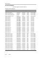
The ADC12 registers are listed in Table 26−2 .
Table 26−2.ADC12 Registers
Register
Short Form
Register Type Address
Initial State
ADC12 control register 0
ADC12CTL0
Read/write
01A0h
Reset with POR
ADC12 control register 1
ADC12CTL1
Read/write
01A2h
Reset with POR
ADC12 interrupt flag register
ADC12IFG
Read/write
01A4h
Reset with POR
ADC12 interrupt enable register
ADC12IE
Read/write
01A6h
Reset with POR
ADC12 interrupt vector word
ADC12IV
Read
01A8h
Reset with POR
ADC12 memory 0
ADC12MEM0
Read/write
0140h
Unchanged
ADC12 memory 1
ADC12MEM1
Read/write
0142h
Unchanged
ADC12 memory 2
ADC12MEM2
Read/write
0144h
Unchanged
ADC12 memory 3
ADC12MEM3
Read/write
0146h
Unchanged
ADC12 memory 4
ADC12MEM4
Read/write
0148h
Unchanged
ADC12 memory 5
ADC12MEM5
Read/write
014Ah
Unchanged
ADC12 memory 6
ADC12MEM6
Read/write
014Ch
Unchanged
ADC12 memory 7
ADC12MEM7
Read/write
014Eh
Unchanged
ADC12 memory 8
ADC12MEM8
Read/write
0150h
Unchanged
ADC12 memory 9
ADC12MEM9
Read/write
0152h
Unchanged
ADC12 memory 10
ADC12MEM10
Read/write
0154h
Unchanged
ADC12 memory 11
ADC12MEM11
Read/write
0156h
Unchanged
ADC12 memory 12
ADC12MEM12
Read/write
0158h
Unchanged
ADC12 memory 13
ADC12MEM13
Read/write
015Ah
Unchanged
ADC12 memory 14
ADC12MEM14
Read/write
015Ch
Unchanged
ADC12 memory 15
ADC12MEM15
Read/write
015Eh
Unchanged
ADC12 memory control 0
ADC12MCTL0
Read/write
080h
Reset with POR
ADC12 memory control 1
ADC12MCTL1
Read/write
081h
Reset with POR
ADC12 memory control 2
ADC12MCTL2
Read/write
082h
Reset with POR
ADC12 memory control 3
ADC12MCTL3
Read/write
083h
Reset with POR
ADC12 memory control 4
ADC12MCTL4
Read/write
084h
Reset with POR
ADC12 memory control 5
ADC12MCTL5
Read/write
085h
Reset with POR
ADC12 memory control 6
ADC12MCTL6
Read/write
086h
Reset with POR
ADC12 memory control 7
ADC12MCTL7
Read/write
087h
Reset with POR
ADC12 memory control 8
ADC12MCTL8
Read/write
088h
Reset with POR
ADC12 memory control 9
ADC12MCTL9
Read/write
089h
Reset with POR
ADC12 memory control 10
ADC12MCTL10
Read/write
08Ah
Reset with POR
ADC12 memory control 11
ADC12MCTL11
Read/write
08Bh
Reset with POR
ADC12 memory control 12
ADC12MCTL12
Read/write
08Ch
Reset with POR
ADC12 memory control 13
ADC12MCTL13
Read/write
08Dh
Reset with POR
ADC12 memory control 14
ADC12MCTL14
Read/write
08Eh
Reset with POR
ADC12 memory control 15
ADC12MCTL15
Read/write
08Fh
Reset with POR
26-20
ADC12
ADC12 Registers
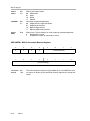
ADC12CTL0, ADC12 Control Register 0
15
14
13
12
11
10
SHT1x
9
8
SHT0x
rw−(0)
rw−(0)
rw−(0)
rw−(0)
rw−(0)
rw−(0)
rw−(0)
rw−(0)
7
6
5
4
3
2
1
0
MSC
REF2_5V
REFON
ADC12ON
ADC12OVIE
ADC12
TOVIE
ENC
ADC12SC
rw−(0)
rw−(0)
rw−(0)
rw−(0)
rw−(0)
rw−(0)
rw−(0)
rw−(0)
Modifiable only when ENC = 0
SHT1x
Bits
15-12
Sample-and-hold time. These bits define the number of ADC12CLK cycles in
the sampling period for registers ADC12MEM8 to ADC12MEM15.
SHT0x
Bits
11-8
Sample-and-hold time. These bits define the number of ADC12CLK cycles in
the sampling period for registers ADC12MEM0 to ADC12MEM7.
SHTx Bits
ADC12CLK cycles
0000
4
0001
8
0010
16
0011
32
0100
64
0101
96
0110
128
0111
192
1000
256
1001
384
1010
512
1011
768
1100
1024
1101
1024
1110
1024
1111
1024
ADC12
26-21
ADC12 Registers
MSC
Bit 7
Multiple sample and conversion. Valid only for sequence or repeated modes.
0
The sampling timer requires a rising edge of the SHI signal to trigger
each sample-and-conversion.
1
The first rising edge of the SHI signal triggers the sampling timer, but
further sample-and-conversions are performed automatically as soon
as the prior conversion is completed.
REF2_5V
Bit 6
Reference generator voltage. REFON must also be set.
0
1.5 V
1
2.5 V
REFON
Bit 5
Reference generator on
0
Reference off
1
Reference on
ADC12ON
Bit 4
ADC12 on
0
ADC12 off
1
ADC12 on
ADC12OVIE Bit 3
ADC12MEMx overflow-interrupt enable. The GIE bit must also be set to
enable the interrupt.
0
Overflow interrupt disabled
1
Overflow interrupt enabled
ADC12
TOVIE
Bit 2
ADC12 conversion-time-overflow interrupt enable. The GIE bit must also be
set to enable the interrupt.
0
Conversion time overflow interrupt disabled
1
Conversion time overflow interrupt enabled
ENC
Bit 1
Enable conversion
0
ADC12 disabled
1
ADC12 enabled
ADC12SC
Bit 0
Start conversion. Software-controlled sample-and-conversion start.
ADC12SC and ENC may be set together with one instruction. ADC12SC is
reset automatically.
0
No sample-and-conversion-start
1
Start sample-and-conversion
26-22
ADC12
ADC12 Registers
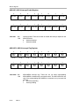
ADC12CTL1, ADC12 Control Register 1
15
14
13
12
11
CSTARTADDx
10
SHSx
9
8
SHP
ISSH
rw−(0)
rw−(0)
rw−(0)
rw−(0)
rw−(0)
rw−(0)
rw−(0)
rw−(0)
7
6
5
4
3
2
1
0
ADC12DIVx
rw−(0)
rw−(0)
ADC12SSELx
rw−(0)
rw−(0)
rw−(0)
ADC12
BUSY
CONSEQx
rw−(0)
rw−(0)
r−(0)
Modifiable only when ENC = 0
CSTART
ADDx
Bits
15-12
Conversion start address. These bits select which ADC12
conversion-memory register is used for a single conversion or for the first
conversion in a sequence. The value of CSTARTADDx is 0 to 0Fh,
corresponding to ADC12MEM0 to ADC12MEM15.
SHSx
Bits
11-10
Sample-and-hold source select
00 ADC12SC bit
01 Timer_A.OUT1
10 Timer_B.OUT0
11 Timer_B.OUT1
SHP
Bit 9
Sample-and-hold pulse-mode select. This bit selects the source of the
sampling signal (SAMPCON) to be either the output of the sampling timer or
the sample-input signal directly.
0
SAMPCON signal is sourced from the sample-input signal.
1
SAMPCON signal is sourced from the sampling timer.
ISSH
Bit 8
Invert signal sample-and-hold
0
The sample-input signal is not inverted.
1
The sample-input signal is inverted.
ADC12DIVx
Bits
7-5
ADC12 clock divider
000 /1
001 /2
010 /3
011 /4
100 /5
101 /6
110 /7
111 /8
ADC12
26-23
ADC12 Registers
ADC12
SSELx
Bits
4-3
ADC12 clock source select
00 ADC12OSC
01 ACLK
10 MCLK
11 SMCLK
CONSEQx
Bits
2-1
Conversion sequence mode select
00 Single-channel, single-conversion
01 Sequence-of-channels
10 Repeat-single-channel
11 Repeat-sequence-of-channels
ADC12
BUSY
Bit 0
ADC12 busy. This bit indicates an active sample or conversion operation.
0
No operation is active.
1
A sequence, sample, or conversion is active.
ADC12MEMx, ADC12 Conversion Memory Registers
15
14
13
12
11
10
9
8
0
0
0
0
r0
r0
r0
r0
rw
rw
rw
rw
7
6
5
4
3
2
1
0
rw
rw
rw
Conversion Results
Conversion Results
rw
rw
Conversion
Results
26-24
Bits
15-0
ADC12
rw
rw
rw
The 12-bit conversion results are right-justified. Bit 11 is the MSB. Bits 15-12
are always 0. Writing to the conversion memory registers will corrupt the
results.
ADC12 Registers
ADC12MCTLx, ADC12 Conversion Memory Control Registers
7
6
EOS
rw−(0)
5
4
3
2
SREFx
rw−(0)
rw−(0)
1
0
rw−(0)
rw−(0)
INCHx
rw−(0)
rw−(0)
rw−(0)
Modifiable only when ENC = 0
EOS
Bit 7
End of sequence. Indicates the last conversion in a sequence.
0
Not end of sequence
1
End of sequence
SREFx
Bits
6-4
Select reference
000 VR+ = AVCC and VR− = AVSS
001 VR+ = VREF+ and VR− = AVSS
010 VR+ = VeREF+ and VR− = AVSS
011 VR+ = VeREF+ and VR− = AVSS
100 VR+ = AVCC and VR− = VREF−/ VeREF−
101 VR+ = VREF+ and VR− = VREF−/ VeREF−
110 VR+ = VeREF+ and VR− = VREF−/ VeREF−
111 VR+ = VeREF+ and VR− = VREF−/ VeREF−
INCHx
Bits
3-0
Input channel select
0000 A0
0001 A1
0010 A2
0011
A3
0100 A4
0101 A5
0110
A6
0111
A7
1000 VeREF+
1001 VREF− /VeREF−
1010 Temperature sensor
1011
(AVCC – AVSS) / 2
1100
(AVCC – AVSS) / 2, A12 on ’FG43x and ’FG461x devices
1101
(AVCC – AVSS) / 2, A13 on ’FG43x and ’FG461x devices
1110
(AVCC – AVSS) / 2, A14 on ’FG43x and ’FG461x devices
1111
(AVCC – AVSS) / 2, A15 on ’FG43x and ’FG461x devices
ADC12
26-25
ADC12 Registers
ADC12IE, ADC12 Interrupt Enable Register
15
14
13
12
11
10
9
8
ADC12IE15
ADC12IE14
ADC12IE13
ADC12IE12
ADC12IE11
ADC12IE10
ADC12IE9
ADC12IE8
rw−(0)
rw−(0)
rw−(0)
rw−(0)
rw−(0)
rw−(0)
rw−(0)
rw−(0)
7
6
5
4
3
2
1
0
ADC12IE7
ADC12IE6
ADC12IE5
ADC12IE4
ADC12IE3
ADC12IE2
ADC12IE1
ADC12IE0
rw−(0)
rw−(0)
rw−(0)
rw−(0)
rw−(0)
rw−(0)
rw−(0)
rw−(0)
ADC12IEx
Bits
15-0
Interrupt enable. These bits enable or disable the interrupt request for the
ADC12IFGx bits.
0
Interrupt disabled
1
Interrupt enabled
ADC12IFG, ADC12 Interrupt Flag Register
15
14
13
12
11
10
9
8
ADC12
IFG15
ADC12
IFG14
ADC12
IFG13
ADC12
IFG12
ADC12
IFG11
ADC12
IFG10
ADC12
IFG9
ADC12
IFG8
rw−(0)
rw−(0)
rw−(0)
rw−(0)
rw−(0)
rw−(0)
rw−(0)
rw−(0)
7
6
5
4
3
2
1
0
ADC12
IFG7
ADC12
IFG6
ADC12
IFG5
ADC12
IFG4
ADC12
IFG3
ADC12
IFG2
ADC12
IFG1
ADC12
IFG0
rw−(0)
rw−(0)
rw−(0)
rw−(0)
rw−(0)
rw−(0)
rw−(0)
rw−(0)
ADC12IFGx
26-26
Bits
15-0
ADC12
ADC12MEMx Interrupt flag. These bits are set when corresponding
ADC12MEMx is loaded with a conversion result. The ADC12IFGx bits are
reset if the corresponding ADC12MEMx is accessed, or may be reset with
software.
0
No interrupt pending
1
Interrupt pending
ADC12 Registers
ADC12IV, ADC12 Interrupt Vector Register
15
14
13
12
11
10
9
8
0
0
0
0
0
0
0
0
r0
r0
r0
r0
r0
r0
r0
r0
7
6
5
4
3
2
1
0
0
0
r0
r0
ADC12IVx
Bits
15-0
ADC12IVx
r−(0)
r−(0)
r−(0)
0
r−(0)
r−(0)
r0
ADC12 interrupt vector value
ADC12IV
Contents
Interrupt Source
Interrupt Flag
000h
No interrupt pending
−
002h
ADC12MEMx overflow
−
004h
Conversion time overflow
−
006h
ADC12MEM0 interrupt flag
ADC12IFG0
008h
ADC12MEM1 interrupt flag
ADC12IFG1
00Ah
ADC12MEM2 interrupt flag
ADC12IFG2
00Ch
ADC12MEM3 interrupt flag
ADC12IFG3
00Eh
ADC12MEM4 interrupt flag
ADC12IFG4
010h
ADC12MEM5 interrupt flag
ADC12IFG5
012h
ADC12MEM6 interrupt flag
ADC12IFG6
014h
ADC12MEM7 interrupt flag
ADC12IFG7
016h
ADC12MEM8 interrupt flag
ADC12IFG8
018h
ADC12MEM9 interrupt flag
ADC12IFG9
01Ah
ADC12MEM10 interrupt flag
ADC12IFG10
01Ch
ADC12MEM11 interrupt flag
ADC12IFG11
01Eh
ADC12MEM12 interrupt flag
ADC12IFG12
020h
ADC12MEM13 interrupt flag
ADC12IFG13
022h
ADC12MEM14 interrupt flag
ADC12IFG14
024h
ADC12MEM15 interrupt flag
ADC12IFG15
Interrupt
Priority
Highest
Lowest
ADC12
26-27
26-28
ADC12