1
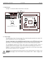
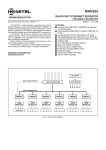
ispLSI5256VA - Demoboard User Manual Version 1.1 We are aware of the fact, that very few designers read manuals. Nevertheless we recommend to read this manual before starting to work with the demoboard. A lot of FAQ's are answered here. Copyright 1999 Bosshard Elektronik. All brand or product names are trademarks or registerd trademarks of their respective holders. The specifications and information herein are subject to change without notice. Bosshard Elektronik, Undelstrasse 48, CH-8493 Saland, Switzerland Tel. +41 (0)52 394 13 13; Fax +41 (0)52 394 13 14; www.bosshard-elektronik.ch May 2000 ispLSI5256VA - Demoboard 0. User Manual May 2000 Kit Contents Please check the contents of the box when receiving the demoboard. It should contain the following items: • ispLSI5256VA - Demoboard • Application example description • This Manual • The schematic of the board We do not ship any software with the board. The application-examples can be downloaded from our website (www.bosshard-elektronik.ch) 1. Introduction This demoboard was designed to give an easy access to the features of the Lattice 5kVA-Family for design engineers. The popularity of this CPLD-family is growing rapidly. Please refer to Lattice documentation or homepage for more details on the architecture and capabilities of this device family. The board can be used for prototyping as well as for design-verification, performance tests, education purposes, evaluation of the 5kVA CPLD family or simply to play around with it and have some fun. 2. Features • • • • • • • • Equipped with an ispLSI5256VA-100LB208. Translation: In-System programmable 3.3VCPLD with 256 Macrocells, specified to run at max. 100MHz in a BGA208 package. On-board 3.3V voltage-regulator On-board oscillator running at 4MHz All device-pins are available on standard single or double row headers Prototyping area for your own circuitry In-System programmable via JTAG-Port. Use the Lattice Download-Cable for direct download from the PC parallel-port to the demoboard. 4 Digit LED display User switches connected to CPLD: • 4 User-Keys • Reset-Key • 8 DIP-switches Bosshard Elektronik 2 www.bosshard-elektronik.ch ispLSI5256VA - Demoboard User Manual May 2000 3. Board Layout Use figure 1 to locate the different components on the board. +5V in GND VCC out X7 1 X3 1 SW1 D1 D2 http://www.bosshard-elektronik.ch D3 D4 Evaluationboard 5256VA Power 1 2 3 4 5 6 7 8 TA1 TA2 TA3 TA4 Reset a col f g b ispLSI 5256VA X4 Y1 Y3 Y5 X2 Y2 Y4 c e d dp X5 Segment allocation for D1 - D4 1 X6 1 1 1 X1 Figure 1. ispLSI5256VA Demoboard Layout 4. Power Supply The board needs a 5 Volt / 1A power-supply. The on-board regulator generates the needed 3.3V, which is available at X7 for use in other peripherals. The power consumption of the ispLSI5256VA depends mainly on your JEDEC-file and the clock frequency. This varies the current available from the 3.3V output, but even in worst case you can draw 100mA. The onboard voltage regulator is overcurrent- and overtemperature-protected. The ispLSI5256VA supports 2.5V VCCIO, which need to be supplied externally. Jumper Y1 connects VCCIO to the 3.3V-supply. Jumper Y2 connects the VCCIO device pin to X6, Pin 11. REMARK: To clarify the VCCIO-issue: It is optional to supply 2.5V for VCCIO and is only needed, when you want to interface to 2.5V - components. CAUTION: Do not feed external 2.5V with Jumpers Y1 and Y2 both set! Set Y1 for VCCIO = 3.3V (from on-board supply) or set Y2 for VCCIO = 2.5V (connect a 2.5V / 30mA - supply to X6, Pin 11). Bosshard Elektronik 3 www.bosshard-elektronik.ch ispLSI5256VA - Demoboard User Manual May 2000 5. Clocks, Output Enables and Reset/Preset All clocking options available from the ispLSI5256VA are usable on this board. For testapplications an on-board oscillator running at 4MHz is connected via jumper Y3 to the CLK2 - pin. Figure 3 shows the clock structure of the device. You can see here, why we chosen CLK2 for the onboard clock - it's the most flexible one because it can be used inverted (internal clock-line CLK2) and non-inverted (internal clock-line CLK3) at the same time. In case the clock-signal is used in product-terms the CLK2-pin is configured as I/O –pin by software. Figure 3. ispLSI5256VA clock structure Jumper Y4 connects the CLK2 pin to X6, pin 5. If you want to feed an external clock to CLK2 or use it as I/O, set jumper Y4 and remove jumper Y3. CAUTION: Do not feed an external clock signal to X6, pin5 with both Y3 and Y4 set. You will probably kill your clock source, the onboard-oscillator or both! All connections for X6 are listed in table1. Device-pin VCC GND CLK0 CLK1 CLK2 / IO 89 CLK3 / IO 98 GSET/GRST X6 pin 1 2 3 4 5 6 7 TOE / IO 0 8 GOE0 9 GOE1 10 VCCIO 11 GND 12 Table 1. X6 connections Bosshard Elektronik Remark Use for fast clock Connected via Y4 to X6, via Y3 to onboard osc. On-board RESET-button pulls this pin to GND, a 10kΩ pull-up is connected to this pin Jumper Y5 pulls this pin to GND General Output Enable 0 General Output Enable 1 Connected via Y2 4 www.bosshard-elektronik.ch ispLSI5256VA - Demoboard User Manual May 2000 6. I/O Connections, LED, Switches and pushbuttons All I/O-pins are connected to the headers. The connections are listed in tables 2,3,4 and 5. Every I/O can be selected to run at VCC (3.3V) or VCCIO (2.5V, externally supplied to VCCIO-Pin) by software. Choosing I/Os to run at VCCIO with a floating VCCIO-Pin is not specified in the ispLSI5256VA - datasheet and will show an unpredictable behavior. HINT: Inputs, that run on 3.3V can be driven with a 5V-signal. Outputs are 5V TTL - compatible. To achieve 5V CMOS compatible output-levels, select the open-drain option for the output (in the software) and add an external pull-up. The board features four 7-Segment LED displays with decimal point (dp) and colon (col). The LED segments are ON when the device-pin is driven LOW. Figure 4 shows the segment allocation. a col f g b c e d dp Figure 4. LED display segment allocation The switches SW1 .. SW8 and the pushbuttons TA1 .. TA4 pull the corresponding I/O-pin to GND when switched on or pushed. A 10kΩ pull-up resistor is connected to all of these signals to ensure a logic high on the pin, when the switch is in off position or the pushbutton is not pressed. When connecting external signals to X1, pins 4..19, please take in account these pull-ups. When connecting external signals to X4, your signal-source has to be able to sink approx. 7 mA (current through LED-segments) to drive logic low. X1 Pin 1 2 3 4 5 6 7 8 9 10 11 12 13 14 15 16 17 18 19 20 21 22 23 24 25 Device Pin NC L2 L1 L3 M1 M2 M3 N1 N3 N2 P2 P1 R1 R2 R3 P3 T1 P4 Function VCC GND X1 Pin 26 27 28 29 30 31 32 33 34 35 36 37 38 39 40 41 42 43 44 45 46 47 48 49 50 TA4 TA3 TA2 TA1 SW7 VCC GND SW8 SW6 SW5 SW4 SW3 SW2 VCC GND SW1 VCC Device Pin Function GND R4 R5 P5 T2 R6 T3 VCC GND T4 T5 R7 P6 T6 T7 VCC GND R8 P8 P7 T8 T9 R9 VCC GND Table 2. X1 Pin connections Bosshard Elektronik 5 www.bosshard-elektronik.ch ispLSI5256VA - Demoboard X2 Pin 1 2 3 4 5 6 7 8 9 10 11 12 13 14 15 16 17 18 19 20 21 22 23 24 25 User Manual Device Pin Function VCC GND R10 T10 T11 T12 T13 T14 VCC GND P11 P12 R11 T15 T16 R14 VCC GND R12 P14 P13 R13 R15 P15 VCC May 2000 X2 Pin 26 27 28 29 30 31 32 33 34 35 36 37 38 39 40 41 42 43 44 45 46 47 48 49 50 Device Pin X3 Pin 26 27 28 29 30 31 32 33 34 35 36 37 38 39 40 41 42 43 44 45 46 47 48 49 50 Device Pin Function GND R16 P16 N15 N14 M14 N16 VCC GND M15 M16 L14 L15 L16 K14 VCC GND K15 K16 J14 J15 J16 H16 VCC GND Table 3. X2 Pin connections X3 Pin 1 2 3 4 5 6 7 8 9 10 11 12 13 14 15 16 17 18 19 20 21 22 23 24 25 Device Pin Function VCC GND G16 F14 G15 F16 E14 F15 VCC GND E16 D16 C16 B16 D15 D14 VCC GND A16 C15 B15 A15 B14 NC VCC Function GND C13 A14 C12 B12 A13 A12 VCC GND C11 B11 NC B10 A10 C10 VCC GND B9 C9 A9 A8 C8 C7 VCC GND Table 4. X3 Pin connections Bosshard Elektronik 6 www.bosshard-elektronik.ch ispLSI5256VA - Demoboard X4 Pin 1 2 3 4 5 6 7 8 9 10 11 12 13 14 15 16 17 18 19 20 21 22 23 24 25 User Manual Device Pin B7 A6 A5 C6 B6 A4 A3 A2 C5 B5 B4 C4 C3 C2 B3 B2 A1 D2 Function VCC GND D4A D4B D4C D4D D4E D4F VCC GND D4G D4dp D4col D3A D3B D3C VCC GND D3D D3E D3F D3G D3dp D3col VCC X4 Pin 26 27 28 29 30 31 32 33 34 35 36 37 38 39 40 41 42 43 44 45 46 47 48 49 50 May 2000 Device Pin B1 D3 E2 C1 E3 D1 F2 E1 F1 G2 F3 H2 H3 G3 G1 H1 J2 J3 Function GND D2A D2B D2C D2D D2E D2F VCC GND D2G D2col D2dp D1A D1B D1C VCC GND D1D D1E D1F D1G D1col D1dp VCC GND Table 5. X4 Pin connections 7. JTAG - Interface The JTAG interface can be used for In-System Programming and for Boundary Scan Test. X5 corresponds to the standard Lattice Download cable pinout (see table 6). After programming you should reset the device to ensure proper operation. For details on InSystem Programming and Boundary Scan Test, please refer to the Lattice documentation or the Lattice homepage (www.latticesemi.com). X5 Pin Device Pin 1 2 G14 3 K3 4 NC 5 NC 6 J1 7 8 K2 Table 6. X5 Pin connections (JTAG-Port) Bosshard Elektronik 7 Function VCC TDO TDI TMS GND TCK www.bosshard-elektronik.ch ispLSI5256VA - Demoboard User Manual May 2000 8. Jumper settings Here you find a brief summary of the jumper settings: Jumper Function Y1 connects VCCIO-Pin to VCC(3.3V) Y2 connects VCCIO-Pin to X6, Pin 11 Y3 connects CLK2-Pin to on-board Oscillator Y4 connects CLK2-Pin to X6, Pin 5 Y5 pulls TOE / I/O 0 to GND Table 7. Jumper settings Factory setting ON OFF ON OFF OFF CAUTION: Do not feed an external clock signal to X6, pin5 with both Y3 and Y4 set. You will probably kill your clock source, the onboard-oscillator or both! CAUTION: Do not feed external 2.5V with Jumpers Y1 and Y2 both set! Set Y1 for VCCIO = 3.3V (from on-board supply) or set Y2 for VCCIO = 2.5V (connect a 2.5V / 30mA - supply to X6, Pin 11). 9. Accessories, stuff you may need You need some kind of software to produce the JEDEC-Files for the ispLSI5256VA. At the time, this manual is written, a starter-software is available free of charge from Lattice Semiconductors homepage (www.latticesemi.com). Software, which supports VHDL or Verilog can be purchased for a few hundred dollars, which is a good investment. With any Software you buy from Lattice you get a download-cable. The download-cable can be purchased separately for less than $100.-- at any Lattice Representative or Distributor. The order-code is: PDS4102-DL2 10. Application Examples, Support Application examples for this demoboard can be downloaded from our homepage: www.bosshard-elektronik.ch If you do an interesting, funny, useful, strange or smart application we would be happy to receive a copy. Please include your approval or denial to post your application on our homepage. Customized versions of the Demoboard are possible: • ispLSI5256VA in BGA208 with different speed-grades • ispLSI5384VA in BGA208, all available speed grades • different frequencies for the on-board oscillator • customized silk-screen Please contact [email protected] for pricing / lead-times. Support for any demoboard-related issues can be obtained by contacting [email protected] . Please do not request our support for issues concerning design-software or the ispLSI5256VA device. This is supported by the Lattice Representatives or Distributors in your area. Bosshard Elektronik 8 www.bosshard-elektronik.ch ispLSI5256VA - Demoboard User Manual May 2000 11. Specifications Parameter Supply Voltage Current Consumption VCCIO (optional) Current needed for VCCIO Pin Voltage available at VCCout (X7) Current available from VCCout Operating Temperature Physical Dimension MIN. 4.75 NOMINAL 5.0 2.3 2.5 3.2 100 0 3.3 MAX. 6.0 1.0 2.7 30 3.4 70 100 x 160 UNITS V A V mA V mA °C mm 12. Additional comments Our boards are much better than our english. Any suggestions for improvements on this document are highly welcome. Please email to: [email protected] . Bosshard Elektronik 9 www.bosshard-elektronik.ch