1
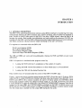
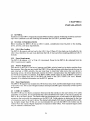
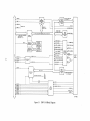
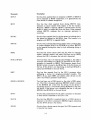
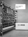
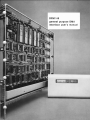
DRV11-B
general purpose DMA
interface user's manual
EK-DRVIB-OP-OOI
DRV11-8
general purpose DMA
interface user's manual
digital equipment corporation • marlborough, massachusetts
1st Edition, August 1976
Copyright © 1976 by Digital Equipment Corporation
The material in this manual is for informational
purposes and is subject to change without notice.
Digital Equipment Corporation assumes no responsibility for any errors which may appear in this
manual.
Printed in U.S.A.
This document was set on DIGITAL's DECset-8000
computerized typesetting system.
The following are trademarks of Digital Equipment
Corporation, Maynard, Massachusetts:
DEC
DECCOMM
DECsystem-10
DECSYSTEM-20
DEC tape
DEC US
DIGITAL
MASSBUS
PDP
RSTS
TYPESET-8
TYPESET-II
UNIBUS
CONTENTS
Page
CHAPTER 1
INTRODUCTION
1.1
1.2
1.3
GENERAL DESCRIPTION
SPECIFICATIONS
RELATED LITERATURE
CHAPTER 2
INSTALLATION
2.1
2.2
2.2.1
2.2.2
2.2.3
2.2.4
2.3
2.4
2.6
2.7
2.8
GENERAL
. . . . . .
SYSTEM CONSIDERATIONS
LSI-II Bus Loading .
Power Requirements
Priority Requirements
Space Requirements .
USER I/O CABLES . . . .
DEVICE ADDRESS SELECTION
INTERRUPT VECTOR ADDRESS SELECTION
MODULE INSTALLATION
INITIAL TURN-ON . . .
DIAGNOSTIC PROGRAM
CHAPTER 3
BASIC OPERATION
3.1
3.2
3.2.1
3.2.1.1
3.2.1.2
3.2.1.3
3.2.1.4
3.2.2
3.2.3
3.2.4
3.2.4.1
3.3
GENERAL
. . . . . .
FUNCTIONAL DESCRIPTION
DRVII-B Registers
Word Count Register (WCR)
Bus Address Register (BAR)
Control/Status Register (CSR)
Input and Output Data Buffer Registers (DBRs)
User Interface Lines . . . . . . . . . . . . . . . . .
LSI-II Bus Lines
................. .
User's I/O Device to LSI-II Memory Transfer (DATO or DATOB)
Interrupts . . . . . . . . . . . . . . . . . . . . . . .
LSI-II Memory to User's Device Transfers (DATIO or DATI)
TIMING . . . . . . . . . . . . . . . . . . . . . . . . . . . . . .
CHAPTER 4
PROGRAMMING
4.1
4.2
4.3
4.3.1
4.3.2
4.3.3
4.3.4
GENERAL
........ .
PROGRAMMING INSTRUCTIONS
DRVI1-B REGISTERS
WCR
BAR
CSR
DBRs
2.5
3.2.5
1-1
1-2
1-4
iii
2-1
2-1
2-1
2-1
2-1
2-1
2-1
2-2
2-2
2-3
2-5
2-5
3-1
3-1
3-1
3-1
3-1
3-1
3-3
3-3
3-4
3-6
3-7
3-7
3-8
4-1
4-1
4-1
4-1
4-1
4-1
4-1
CONTENTS (Cont)
Page
4.4
4.4.1
4.4.2
4.5
PROGRAM INTERRUPTS
Word Count Overflow
CSR ERROR Bit (Bit 15)
FUNCTION AND STATUS BITS
4-2
4-2
4-2
4-2
ILLUSTRATIONS
Figure No.
1-1
2-1
2-2
2-3
2-4
3-1
3-2
3-3
3-4
3-5
3-6
3-7
4-1
Title
DRVll-B Simplified Interface Diagram
DRVll-B Connector and Switch Locations
DRVll-B Device Address Select Format
DRVll-B Interrupt Vector Address Select Format
DRVll-B Connector Pin Assignments ..
DRVll-B Block Diagram . . . . . . . .
DMA DATO/DATOB Data Flow Diagram
DMA DATIO/DATI Data Flow Diagram
DRVll-B Single Cycle, User-Initiated, Timing Diagram
DRVll-B Single Cycle, Program-Initiated, Timing Diagram
DRVll-B Burst Mode, User-Initiated, Timing Diagram
DRVll-B Burst Mode, Program-Initiated, Timing Diagram
CSR Format . . . . . . . . . . . . . . . . . . . . . . . .
Page
1-2
2-3
2-3
2-4
2-4
3-2
3-6
3-8
3-9
3-10
3-11
3-12
4-2
TABLES
Table No.
2-1
3-1
4-1
Title
Page
2-2
3-4
4-3
Recommended Cable Assemblies
CO, C I- Codes
CSR Bit Functions
..... .
iv
CHAPTER 1
INTRODUCTION
1.1 GENERAL DESCRIPTION
The DRVII-B is a general-purpose direct memory access (DMA) interface for transferring 16-bit data
words directly between the LSI-II memory and a user's I/O device. Data Transfer Out (DATO) or
Data Transfer In (DATI) takes place via the LSI-ll bus after a DMA request, where the DRV11-B
becomes bus master. Burst modes, byte addressing, and read-modify-write operation (DATIO) are
possible with the DRVII-B. The DRV11-B features switch-programmable device and vector addresses
and 40-pin connectors which provide for simple interfacing to the user's I/O device.
Five registers are contained within the DRV11-B:
Word Count Register (WCR)
Bus Address Register (BAR)
Control/Status Register (CSR)
Input and Output Data Buffer Registers (DBRs).
The CSR and DBRs are word- and byte-addressable, whereas the WCR and BAR are only wordaddressable.
DR V 11- B operation is initialized under program control by:
1.
Loading the WCR with the 2's complement of the number of transfers
2.
Loading the BAR with the first address to or from which data is to be transferred
3.
Loading the CSR with the desired function bits.
Data transfers may now proceed under the control of the DRV11-B DMA logic.
Figure 1-1 shows the primary interface signals between the DRVII-B and the user's I/O device. DMA
input (DATI) or output (DATO) data transfers take place when the processor clears READY. For a
DATO cycle (DRV11-B to memory transfer), the user's I/O device presets the CONTROL BITS
(word count increment enable, bus address increment enable, C 1, CO, AOO, and A TTN), and asserts
CYCLE REQUEST to gain use of the LSI-II bus. When CYCLE REQUEST is asserted, input data is
latched into the input DBR, the CONTROL BITS are latched into the DRV11-B DMA control, and
BUSY goes low. (A DATI cycle memory to DRV11-B transfer is handled in a similar manner, except
that the output data is latched into the output DBR during the bus cycle.)
1-1
~
16- DATA/ADDRESS BITS
'I
,
16 - OUTPUT DATA BITS
'")
V
READY
,,/
CYCLE REQUEST
en
FUNCTION BITS
:::l
III
DRVll-B
DMA
INTERFACE
:::,
H
STATUS BITS
en
USER'S
I/O
DEVICE
...I
BUSY
CONTROL BITS
BUS CONTROL
~....
""
16-INPUT DATA BITS
7
11- 4155
Figure I-I
DRVII-B Simplified Interface Diagram
When the DRVII-B becomes bus master, a DATO or DATI cycle is performed directly to or from the
LSI-II memory location specified by the BAR. At the end of each cycle, the WCR and BAR are
incremented and BUSY goes high while READY remains low. A second DATO or DATI cycle is
performed when the user's I/O device again asserts CYCLE REQUEST. DMA transfers will continue
asynchronously until the WCR increments to zero, at which time READY goes high and the DR VllB generates an interrupt (if interrupt enable is set) to the LSI-II processor.
If burst mode is selected (SINGLE CYCLE low), only one CYCLE REQUEST is required for the
complete synchronous transfer of the specified number of data words.
1.2 SPECIFICATIONS
The following specifications and particulars are for informational purposes and are subject to change
without notice.
Physical
Quad-height, single width, extended length module
Dimensions
8-1/2 in. L, 10-1/2 in. H, 1/2 in. W
(21.6 cm L, 26.7 cm H,1.27 CITl W)
Weight
13 oz. (370 gr)
1-2
User I/O Connections
Two (2) 40-pin connectors
Mounting Requirements
Plugs directly into LSI-II backplane or LSI-ll expansion backplane
Electrical
Logic Power Requirements
+5 V ± 5% @ 1.9 A (nominal)
LSI-II Bus Loading
Presents one bus load
User Loading
I nput Data Lines
I TTL unit load each
HIGH = Logic one
LOW = Logic zero
Input Control Lines
I TTL unit load each
HIGH = Logic one
LOW = Logic zero
Output Data Lines
10 TTL unit loads (drive) each
HIGH = Logic one
LOW = Logic zero
Output Control Lines
10 TTL unit loads (drive) each
HIGH = Logic one
LOW = Logic zero
Module Type
M7950
Operational
Transfer Mode
DMA or program-controlled with interrupts
Data Transfer Rate
Up to 250,000 16-bit words per second in single cycle mode
Up to 500,000 16-bit words per second in burst mode
Environmental
Temperature
Storage: -40° to 66° C (-40° to 150° F)
Operating: 5° to 50° C (41 ° to 122° F)
Relative Humidity
10% to 95% noncondensing
1-3
1.3 RELATED LITERATURE
In addition to the M7950 print set, the LSI-II PDP-II/03 User's Manual and the LSI-II PDP-I 1/03
Processor Handbook contain useful information for installing and operating the DRVII-B generalpurpose DMA interface. Handbooks may be ordered from the nearest Digital Equipment Corporation
Sales Office.
1-4
CHAPTER 2
INSTALLATION
2.1 GENERAL
Installation of the DRVII-B general-purpose DMA interface consists of selecting the device and interrupt vector addresses and then inserting the interface into an LSI-ll processor system.
2.2 SYSTEM CONSIDERATIONS
Before installing the DRVII-B into an LSI-II system, consideration must be given to bus loading,
power, priority, and space requirements.
2.2.1 LSI-ll Bus Loading
The DRVII-B presents one bus load to the LSI-ll bus. Fifteen (15) bus loads can be handled by the
LSI-II bus; therefore, the user must determine the LSI-ll bus load when installing additional LSI-ll
modules.
2.2.2 Power Requirements
The DRVII-B requires +5 V ± 5% @ 1.9 A (nominal). Power for the DRVII-B is obtained from the
LSI-II system power supply.
2.2.3 Priority Requirements
Each device on the LSI-II bus has an interrupt and DMA priority based on its relative position from
the processor. Since the user may install the DRVII-B on the bus along with other devices that use the
same interrupt or DMA priority, the user must bear in mind that when more than one device is
requesting service, the device electrically nearest the LSI-ll microprocessor has the highest priority
and will be serviced first. In addition, ifthe REVII DMA refresh option is used, the REVII must be at
a priority level higher than that of the DRVII-B. Refer to the- LSI-II PDP-II/03 User's Manual,
Appendix G for detailed information on the REVII options.
2.2.4 Space Requirements
The DRVII-B requires four module slots. Of the four slots, the A and B module fingers must interface
to the LSI-II bus. The C and D fingers maintain interrupt and DMA grant continuity as well as power
and ground.
2.3 USER I/O CABLES
The DRVII-B has two 40-pin connectors which provide the interface to the user's device. Two cable
assemblies are required. It is recommended that cable assemblies from Table 2-1 be used to connect the
DRVII-B to the user's device. The listed cables are terminated (one or both ends) with H856 40-pin
connectors that mate with the connectors on the DRVII-B. Cable selection is determined by the type
of connections used on the user's device. The desired cable length (XX) must be specified when ordering. (Lengths longer than 50 feet are not recommended for use with the DRVII-B.) Cables may be
ordered from the nearest Digital Equipment Corporation Sales Office. Non-standard length caoles
may be ordered at additional cost.
Table 2-1
Recommended Cable Assemblies
Cable No.
Connectors
Type
Standard Lengths (ft./m.)
BC08R-XX
H856 to H856
Shielded flat
1,6,10, 12,20,25,50ft.
0.305, 1.830,3.050,3.66,
6.100,7.625, 15.250 m.
BC04Z-XX
H856 to open
end
Shielded flat
6, 10, 15,25,50 f1.
1.830,3.050,4.575, 7.625,
15.250 m.
2.4 DEVICE ADDRESS SELECTION
The DRVII-B contains five registers:
the
the
the
the
the
WCR
BAR
CSR
input DBR
output DBR.
These registers must be addressed for data and status transfers between the DRVll-B and the LSI-ll
processor. The two (2) DBRs use the same address. The register addresses are sequential by even
numbers and are as follows:
Register
WCR
BAR
CSR
DBRs
BBS7
1
1
1
1
Octal Address
XXXXXO
XXXXX2
XXXXX4
XXXXX6
The assigned DMA interface base address is 7724108. The user selects a base address for assignment to
the WCR and sets the device address selection switches on the DRV11-B module to decode this
address. The remaining BAR, CSR, and DBR addresses are then properly decoded by the module as
they are received from the LSI-II processor.
Figure 2-1 shows the location of the device address selection switches on the DRV11-B module.
Switches are set to the ON (closed) position for bits to be decoded as "ONE" bits in the base address.
Bits decoded as "ZERO" bits in the address have their switches set to the OFF (open) position. Figure
2-2 shows the address select format and presents the switch-to-bit relationship for the device address
selection switches.
2.5 INTERRUPT VECTOR ADDRESS SELECTION
Vector addresses 0-17748 are reserved for LSI-II system users. The DRV11-B is assigned vector
address 1248 • The user selects the interrupt vector address by means of switches on the DRV11-B
module. Figure 2-1 shows the location of the vector address selection switches. Vector address selection switches are set to the ON (closed) position for bits to be encoded as "ONE" bits in the vector
address. Bits encoded as "ZERO" bits in the address have their switches set to the OFF (open) position. Figure 2-3 shows the address select format and presents the switch-to-bit relationship for the
vector address selection switches.
2-2
J1
DEVICE ADDRESS
SELECTION SWITCHES
VECTOR ADDRESS
SELECTION SWITCHES
J2
"''''0
zo
"'''020
_N
.
_UI
-
..
-'"
-01
-UI
-01
-01
-
- ...
-ID
-0
-01
11 - 4156
Figure 2-1
DRVII-B Connector and Switch Locations
DECODED BY BBS7
r-------~A~--
DEVICE
ADDRESS
SELECTION
SWITCHES
______
------I
DECODED FOR
1 OF 4
REGISTERS
SELECTED BY SWITCHES
~V~----------------~A------------------_,
0
2
N
0
F
F
I
3
4
5
6
7
I I I I I
8
9
10
I I
OFF= "ZERO"
ON="ONE"
11-4184
Figure 2-2
DRVII-B Device Address Select Format
2.6 MODULE INSTALLATION
With the exception of the first four slots (the LSI-l 1 processor always occupies the first slots), the
DRVII-B can be installed into any four slots (Paragraph2.2.4) of the LSI-ll backplane. However, if
REVII DMA refresh option is used, the DRVII-B must be at a lower priority than the REV11. When
inserting the module into the backplane, make sure that the deep notch on the module seats against the
connector block rib. Do not insert or remove the module with power applied. After performing the initial
turn-on (Paragraph 2.7), connect the user's I/O cables to 11 and J2 on the DRVII-B I/0 connectors.
Connector locations for the DRVII-B are shown in Figure 2-1. Pin assignments for 11 and J2 are
shown in Figure 2-4 and are specified in Paragraph 1.2.
2-3
4 TH
OCTAL DIGIT
(OOR 4)
1 ST
OCTAL
DIGIT
I
VECTOR
ADDRESS
SELECTION
SWITCHES
2 NO
OCTAL
DIGIT
5
4
3
6
PREASSIGNED
AS ZEROS
I
r - - - . A A - -_____"r------'~--.....,
2
---_........l
3RD
OCTAL
DIGIT
03
02
7
8
~
00
01
I I I I I I I
OFF·"ZERO"
ON· "ONE"
11-4185
Figure 2-3
-=1-
SINGLE CYCLE H
DRVII-B Interrupt Vector Address Select Format
A
B
C
0
E
F
H
J
K
L
M
N
p
R
S
T
U
v
CYCLE REQUEST H
-=1-
IN IT V2 H
READY H
WC INC ENB H
STATUS A H
INIT H
Z
AA BB
7
OUT H
6 OUT H
5 OUT H
4 OUT H
3 OUT H
CC
EE FF
HH JJ
KK LL
MM NN
pp
RR
SS
TT
UU
VV
2 OUT H
lOUT H
a
OUT H
DO
B
0
E
F
H
J
K
L
M
N
p
R
STATUS B H
I
STATUS C H
w x
Y
A
C
I
I
8 OUT H
7 IN H
9 OUT H
6 IN H
10 OUT H
5 IN H
11 OUT H
4 IN H
12 OUT H
3 IN H
13 OUT H
2 IN H
14 OUT H
1 IN H
15 OUT H
a
IN H
S
T
U
V
W
x
Y
Z
AA
BB
CC
DO
EE
FF
HH
JJ
KK LL
MM NN
pp
RR
SS
TT
UU
vv
BUSY H
ATTN H
AOO
H
BA INC ENB H
FNCT 3 H
CO H
FNCT 2 H
Cl
H
I
I
8
IN H
9
IN H
10 IN H
11
IN H
12
IN H
13
IN H
14
IN H
15
IN H
J2
J1
11- 4159
Figure 2-4
DRVII-B Connector Pin Assignments
2-4
2.7 INITIAL TURN-ON
After completing the module installation, turn on the LSI-II and initialize the system. With no I/O
cables connected, and using the LSI-ll terminal and operating procedures, perform the following:
I.
Load the addresses of the WCR, BAR, CSR, and DBRs through the system terminal and
examine the locations. The terminal will indicate the following:
WCR contents will be 000000
BAR contents will be 000001
CSR contents will be 127200
DBR contents will be 177777
2.
The WCR and BAR can be loaded with data from the system terminal and the corresponding data read back on the terminal. BAR bit 0 will read as a one (1) with no I/O cables
connected.
The user's I/O device cables can now be connected to the DRVII-B (Figure 2-1).
2.8 DIAGNOSTIC PROGRAM
The check procedure performed in Paragraph 2.7 does not completely verify the operation of the
DRVII-B. Complete module operation can be verified through the use of the diagnostic software
program MAINDEC-MD-II-DVDRA-PB. The program can be loaded into the LSI-II system by
means of a paper tape reader or a terminal. A BC08R maintenance cable (not longer than 50 ft) is
required to loop the DBR output to the DBR input for checking the I/O data path. A complete
description of the diagnostic software program and its implementation is provided in MAINDECMD-II-DVDRA-D.
2-5
CHAPTER 3
BASIC OPERATION
3.1 GENERAL
This chapter contains a functional description of the DRVII-B. The DRVII-B registers are described
as well as user device and bus operations necessary to perform DMA transfers. Figure 3-1 is a block
diagram of the DRVII-B. All descriptions are written to this diagram. The chapter ends with a brief
description of the timing associated with DMA transfers.
3.2
FUNCTIONAL DESCRIPTION
3.2.1 DItVII-B Registers
The DRVll-B contains five (5) registers:
Word Count Register (WCR)
Bus Address Register (BAR)
Control Status Register (CSR)
Input and Output Data Buffer Registers (DBRs).
3.2.1.1 Word Count Register (WCR) - The WCR is a I6-bit read/write register that controls the
number of transfers. This register is loaded (under program control) with the 2's complement of the
number of words to be transferred. At the end of each transfer, the word count register is incremented.
When the contents of the WCR is incremented to zero, transfers are terminated, READY is set, and if
enabled, an interrupt is requested. The WCR is word-addressable only.
3.2.1.2 Bus Address Register (BAR) - The BAR is a IS-bit read/write register. This register is loaded
(under program control) with a bus address (not including address bit 0) which specifies the location to
or from which data is to be transferred. The BAR is incremented after each transfer and can be
incremented across 32K memory boundaries via the extended address feature of the DRVII-B. Systems with only 16 address bits will "wrap-around" to location zero when the extended address bits are
incremented. The BAR is word-addressable only ..
3.2.1.3 Control/Status Register (CSR) - The CSR is a 16-bit register used to control the functions
and monitor the status of the interface. Bit 00 is a write-only bit and always reads as a zero. Bits 01-06,
and bits 08 and 12 are read/write bits, while bits 07, 09-11, and 13-15 are read-only bits. Bit 14 can be
written to a zero. Bits 04 and 05 are the extended addressing bits. CSR bit functions are fully described
in Chapter 4. The CSR is both byte- and word-addressable.
3-1
~
~
BWTBT L
BBS7 L
BAD 16L
BAD 17L
'"
AOO H
BA INC ENB H
WORD COUNT
~'--""(D-A.;;.0.;;..0--1;..;;5-H;.;.)__1\.",
3-STATE BUS (DATAl ADDRESS BITS DA 00-15H)
"
TRANSCEIVERS
VA
VECTOR
/ "
ADDRESS "
V2 -V9
GENERATOR
"
DEVICE
I SELECTION
ADDRESS
I
I
./
ATTN
READY H
(DAI3)
-'
ATTN H
C~TNlru~L
CYCLE (DAOS)
I"'p>-r'==-'-"="--'------J
BIAKO
BIRO
L
L
LOG IC
XAD 16,17 (DA04 ,05)
FNCT 1,2,3,(DAOI,02,03)
IE (1) H
L
PROTOCOL
LOGIC
REGISTER SELECTS
BDOUT
BDMR
BSACK
BDMGO
BDMGI
BRPLY
BDIN
BSYNC
L
L
L
L
L
L
L
L
i
i
ABCH
REGISTER
CYCLE
(CSR )
~R:;-;E"'O~U='=E-=ST=-cH,--~
USER'S
~.
DEVICE
~
}
~
IE (I) H
_ _ _ _ _ _ _ _ _ _ _ _I L______
16 L
BAD
GO (DA 0)
~r---__~M~0~1~2~H
STAT
IE (DA06)
1
BWTBT
1 2 3 H
STATUS A,B,C(DAll,10,09)
SWITCHES
m~~B~I~N~I~TLJL~________r---------~-BRfE~A~DY~(lIL)JH~--------------~------__JI
~_~--"B-"'I"'A"'K"'I'------'L~______-+l I NTE RRU PT
III
FNCT
MAINT (DAI2)
READY (DA07)
I
WC INC ENB H
ERROR (DAI5)
::J
N
WORD
COUNT
REGISTER
(WCR)
I-.- NEX (DAI4)
III
W
~
R~g~~ERr-------------~V'/
'\.7
DEVICE
DEVICE
ADDRESS
ADDRESS ~ A3 - AI21 SELECT ION
SELECTOR"
SWITCHES
""'-
BUFFER
DDRESS
(DA 00-15H)
16-BUS DATA IADDRESsV
VECTOR BITS
(BDAL 00 - 15 L)
BBS7 L
OUTPUT DATA BITS
(0-15 OUT H)
L.]/'\[~
} FROM CSR
V
~
OgX~~T
BUS
ADDRESS
REGISTER
(BAR)
INPUT
DATA
BUFFER
(DBR)
TO
CSR
WCR
BAR
DBR'S
1/0
TO
LSI~11
BUS
K'~~I~N~P~U~T~D~A~T~A~B~I=TS~-4
(0-15INH)
SYNC
DIN
CO H
CI H
DMA
CONTROL
LOGIC
SINGLE CYCLE H
V
INIT H
INIT V2 H
11-4160
Figure 3-1
DRVII-B Block Diagram
3.2.1.4 Input and Output Data Buffer Registers (DBRs) - The two DBRs are 16-bit registers. The
input DBR is a read-only register; the output DBR is a write-only register. Data is loaded into the
input DBR by the user's device and subsequently transferred to memory under DMA control by the
DRVII-B, or under program control by the LSI-ll processor. Conversely, data is written into the
output DBR from memory under DMA control by the DRVII-B, or under program control by the
LSI-II processor, and read by the user's device. The input and output DBRs interface to the user's
device by means of two separate 40-pin I/O connectors. These connectors may be cabled together (for
maintenance purposes) to function as a read/write register. The input and output DBRs share the
same bus address and are byte- and word-addressable.
3.2.2 User Interface Lines
There are 50 interface lines (25 per connector) between the DRVII-B and the user's I/O device. Of
these lines, 32 are I/O data lines, 3 are for status, and 15 are for control. A brief description of these
interface lines follows:
Mnemonic
Description
00 OUT - 15 OUT
16 TTL data output lines from the DRVII-B. One
00 IN - 15 IN
16 TTL data input lines from the user's device. One = high.
STATUS A, B, C
Three TTL status input lines from the user's device. The function of these lines is defined by the user.
FUNCT 1,2,3
Three TTL output lines to the user's device. The function of
these lines is defined by the user.
INIT
One TTL output line; used to initialize the user's device.
INIT V2
One TTL output line; present when INIT is asserted or when
FUNCT 2 is written to a one. Used for interprocessor buffer
applications.
AOO
One TTL input line from the user's device. This line is normally
high for word transfers. During byte transfers this line controls
address bit 00.
BUSY
One TTL output line to the user's device. BUSY is low when the
DRVI1-B DMA control logic is requesting control of the LSI11 bus or when a DMA cycle is in progress. A low-to-high transition indicates end of cycle.
READY
One TTL output line to the user's device. When the READY
line goes low D MA transfers may be initiated by the user's
device.
CO, CI
Two (2) TTL input lines from the user's device. These lines control the LSI-ll bus cycle for DMA transfers. CO, C 1 codes for
the four (4) possible bus cycles are listed in Table 3-1.
3-3
= high.
Mnemonic
Description
Table 3-1
SINGLE CYCLE
CO, Cl Codes
Bus Cycle
CO
Cl
DATI
DATIP
DATO
DATOB
o
1
o
o
o
1
1
1
One TTL input line from the user's device. This line is internally
pulled high for normal DMA transfers. For burst mode operation SINGLE CYCLE is driven low by the user's device.
CAUTION
When single cycle is driven low, total system operation is affected because the LSI-ll bus becomes
dedicated to the DMA device and other devices,
including the MOS memory refresh function, cannot
use the bus.
WC INC ENB
One TTL input line from the user's device. This line is normally
high to enable incrementing the DRVII-B word counter. Low
inhibits incrementing.
BA INC ENB
One TTL input line from the user's device. This line is normally
high to enable incrementing the bus address counter. Low
inhibits incrementing.
CYCLE REQUEST
One TTL input line from the user's device. A low-to-high transition of this line initiates a D MA request.
ATTN
One TTL input line from the user's device. This line is driven
high to terminate DMA transfers, to set READY and request
an interrupt if the interrupt enable bit is set.
3.2.3 LSI-ll Bus Lines
There are 34 LSI-II bus signal lines used by the DRV11-B; 16 of these are multiplexed and bidirectional lines which carry data and address bits. Two lines are used for extended address bits, while 16 lines
are used for control signals. A brief description of the 34 bus lines follows:
Mnemonic
Description
BDAL 0 - BDAL 15
16 bus datal address lines. An address is first placed on these
lines followed by the data. These lines are asserted when driven
low.
BAD 16, 17
Two (2) bus lines used to address beyond 32K of memory by the
DRV11-B. These lines are asserted when low.
BDOUT
One bus line; when asserted (low) indicates that data is available
on the BDAL lines and an output transfer (with respect to the
bus master) is taking place.
3-4
. Mnemonic
Description
BRPLY
One bus line; asserted (low) in response to BDIN or BDOUT
and in response to BIAK transactions. It is generated by the
slave device for address recognition.
BDIN
One bus line; when asserted (low) during BSYNC time,
indicates an input transfer (with respect to the bus master).
Requires a BRPL Y response. BDIN is asserted when the bus
master is ready to accept data from the slave. When asserted
without BSYNC, indicates that an interrupt operation is
occurring.
BSYNC
One bus line; asserted (low) by the bus master to indicate that it
has placed an address on the BDAL lines. The transfer is in
progress until BSYNC is negated (high).
BWTBT
One bus line; asserted (low) during address time to indicate that
an output sequence (DATO or DATOB) is to follow. BWTBT
is also asserted during data time for byte addressing during a
DATOB.
BIRQ
One bus line; device asserts (low) this line when its interrupt
enable, interrupt request, and ready flip-flops are set. BIRQ
informs the LSI-II processor that service is requested.
BIAKI, BIAKO
Two bus lines; one (I) is interrupt acknowledge in, the other is
interrupt acknowledge out. BIAKI is generated by the LSI-ll
processor in response to BIRQ. The processor asserts (low)
BIAKO which is routed to the BIAKI pin of the first device on
the bus. If the device is not requesting an interrupt BIAKO is
passed (as BAIAKI) to the next device.
BBS7
One bus line; asserted (low) by the LSI-II processor when
addressing a device for program-controlled transfers. The
DRVII-B can assert BBS7 and address other devices on the
LSI-II bus without processor intervention.
BDMGi, BDMGO
Two bus lines; one is DMA grant in, the other is DMA grant
out. The LSI-II processor generates BDMGO which is routed
to the BDMGI pin of the first bus device. If the device is
requesting the bus, it will inhibit passing BDMGO to the next
bus device. If the device is not requesting the bus, it will pass
BDMGO (as BDMGI) to the next device.
BINIT
One bus line; asserted (low) by the LSI-II processor to initialize
or clear devices connected to the LSI-II bus.
BSACK
One bus line; BSACK is asserted (low) by a DMA device in
response to the LSI-II processor's BDMGO signal, indicating
that the 0 MA device is bus master.
BDMR
One bus line; a device asserts this signal for DMA requests and
to become bus master.
3-5
3.2.4 User's I/O Device to LSI-ll Memory Transfer (DA TO or DATOB)
Data transfers from the user's I/O device to the LSI-II memory are DMA transfers. Figure 3-2 illustrates the data flow for a DMA DATO or DATOB cycle. Referring to Figure 3-1, DMA transfers are
initialized under program control by loading the DRVII-B WCR (in 2's complement) with a count
equal to the number of words to be transferred; loading the BAR ~ith the starting memory address for
word storage; and setting the CSR for transfers.
~
'"
,...
-
~
/l
f-'
'\
DRVII-S
./
"'"
__
DATO
OR
~
r
f-'
'--
DATOS
--
USERS
DEVICE
J
(J)
:J
m
\.=::;
DATA FLOW_
H
v~
~l/t
~
~
./
K
-"
-vi
MEMORY
LSI-II
PROCESSOR
'7
11- 4187
Figure 3-2
DMA DATO/DATOB Data Flow Diagram
When the GO bit of the CSR is written to a "one," READY goes low and the user's I/O device
conditions the ADO, BA INC ENB, WC INC ENB, ATTN, SINGLE CYCLE (high for normal DMA
transfers), and the CO, Cl (refer to Table 3-1) lines, and then asserts CYCLE REQUEST. The INPUT
DATA BITS and control bits (CO, Cl and SINGLE CYCLE) are latched into the respective DRVII-B
registers. CYCLE REQUEST sets CYCLE and causes the DRVII-B to assert BDMR which makes
an LSI-ll bus request and causes BUSY to go low. In response to BDMR, the processor asserts
BDMGOwhich is received as BDMGI. The DRVII-B becomes bus master and asserts BSACK and
negates BDMR. The processor then terminates the bus grant sequence by negating BDMGO.
As bus master, the DRVl1-B performs a DATO or DATOB bus cycle by placing the memory address
on BDAL lines, asserting BWTBT, and then asserting BSYNC. The LSI-ll memory decodes the
address; then, the DRVl1-B removes the address from the BDAL lines, negates BWTBT (BWTBT will
remain active for a DA TOB) and then places the user's input data on the BDAL lines and asserts
BDOUT. Memory receives the data and asserts BRPLY. In response to BRPLY, the DRVII-B
negates BDOUT and then removes the user's input data from the BDAL lines. Memory now negates
BRPLY, the bus cycle is terminated, and the bus is released when the DRVll-B negates BSACK and
BSYNC.
3-6
At the end of the first transfer, the DRVII-B WCR and BAR are incremented, BUSY goes high, while
READY remains low. With BUSY high and READY low, the user's I/O device can initiate another
DATO or DA TOB cycle by again asserting CYCLE REQUEST. DMA transfers can continue until
the WCR increments to zero and generates an interrupt request, if the interrupt enable bit is set.
3.2.4.1 Interrupts - When the WCR increments to zero, READY goes high and the DRVII-B generates an interrupt request (if the interrupt circuits are enabled). The LSI-II processor responds to the
interrupt request (BIRQ) by asserting BDIN followed by BIAKI (interrupt acknowledge). BIAKI is
received by the DRVII-B and in response places a vector address on the BDAL lines, asserts BRPLY,
and negates BIRQ. The LSI-II processor receives the vector address and negates BDIN and BIAKI.
The DRVII-B now negates BRPL Y, while the processor exits from the main program and enters a
service program for the DRVII-B as indicated by the vector address.
Interrupt requests from the DRVII-B occur for the following conditions:
I.
When the WCR increments to zero - this is a normal interrupt at the end of a designated
number of transfers.
2.
When the user's I/O device asserts ATTN - this is a special condition interrupt which may
be defined by the user to override the WCR.
3.
When a nonexistent memory location is addressed by the DRVII-B - this special condition
interrupt is produced when no BRPL Y is received from the LSI-II memory.
Interrupts are explained in greater detail in Chapter 4 of this manual.
3.2.5 LSI-ll Memory to User's Device Transfers (DATIO or DATI)
DMA transfers from the LSI-II memory to the user's I/O device occur in a manner similar to that
described for user's I/O device to memory transfers. Figure 3-3 illustrates the data flow for a DMA
DATIO or DATI cycle. Under program control, the DRVll-B WCR (Figure 3-1) is loaded with a
count equal to the number of transfers, while the BAR is loaded with the starting address from which
the first word will come; the CSR is set for transfers.
With the CSR set, READY goes low and the user's I/O device conditions the CO, Cl lines (refer to
Table 3-1) for a DATI or a DATIO and conditions the WC INC ENB, BA INC ENB, ATTN,
SINGLE CYCLE (high for normal DMA transfers), and asserts CYCLE REQUEST. BUSY from the
DRVII-B goes low and the user's control bits are latched into the DRVII-B. The DRVII-B then
asserts BDMR which makes a bus request. When the request is arbitrated as described in Paragraph
3.2.4, the DRVII-B becomes bus master.
When the DRVII-B becomes bus master, a DATI or DATIO bus cycle is performed (a DATI is
described). The DRVII-B places the address of the memory location from which the first word is
taken on the BDAL lines and asserts BSYNC. Memory decodes and latches the address. The DR Vl1B then removes the address from the BDAL lines and asserts BDIN. Input data is now placed on the
BDAL lines by the memory and the memory asserts BRPLY. The input data is accepted by the
DRVII-B and BDIN is negated. Memory negates BRPLY and the DRVII-B negates BSACK and
BSYNC to terminate the bus cycle and release the bus. The OUTPUT DATA BITS for the user's I/O
device are stored in the DRVII-B output data buffer register. These bits can be read by the user's
device at the low-to-high transition of BUSY.
3-7
DRVII-8
_
til
::::l
m
~
DATA FLOW -
DATI OR
USERS
DEVICE
DATIO_
---....II
MEMORY
LSI-II
PROCESSOR
11- 418 8
Figure 3-3
DMA DATIO/DATI Data Flow Diagram
At the end of the first transfer, the DRVI1-B WCR and BAR are incremented, BUSY goes high, while
READY remains low. The user's device can initiate another DATI or DATIO cycle by again setting
CYCLE REQUEST. DMA transfers to the user's device can continue until the WCR increments to
zero and causes an interrupt request to be generated (Paragraph 3.2.4.1).
3.3 TIMING
Input and output timing for the DRVII-B is shown in Figures 3-4 through 3-7. The timing diagrams
show user signal timing for single cycle and burst mode operations which can be either program- or
user-initiated.
3-8
I.~---
1ST CYCLE - - - - ....
READY
LAST CYCLE
NTH CYCLE
(OUTPUT)
1--------1
J
250n5 MIN.
==J
WC INC ENB, BA INC ENB,
CO, Cl, ATTN, AOO,
DATA IN*
(INPUTS)
I
I
I
I
SINGLE CYCLE (INPUT)
MIN.
-1
1
1
I
I;
1
1
--1
0 ns MIN.
1 ; 0 n5 MIN.
Yo)
I
\0
CyCl.. E REQUEST (INPUT)
o ns
t
14-S MIN.
D~~"SM~~~1
MIN.
MIN.
BUSY (OUTPUT)
250n5 MIN.
250ns MIN.
250 ns MIN.
DATA OUT * *
LEGEND:
*
= DATO
**
= DATI OR DATIO BUS CYCLE;
OR DATOB BUS CYCLE;
C1
=1
C1 = 0
11-4161
Figure 3-4 DRVll-B Single Cycle, User-Initiated, Timing Diagram
1ST CYCLE
-----.tool~I----- NTH CYCLE
LAST CYCLE
LOW HERE WHEN USED TO SET-UP THE CONTROL INPUTS
READY
(OUTPUT)
WC INC ENS, SA INC ENS,
CO, Cl, ATTN, AOO,
DATA IN"
(INPUTS)
SINGLE CYCLE (INPUT)
I
I
I
-1
Irons MIN.
W
I
.-
o
CYCLE REQUEST (INPUT)
BUSY (OUTPUT)
250ns MIN
250ns MIN.
250ns MIN.
DATA OUT**
LEGEND:
II
= DATO OR DATOS SUS CYCLE; Cl = 1
"" = DATI OR DATIO SUS CYCLE; Cl = 0
" -4277
Figure 3-5
DRVII-B Single Cycle, Program-Initiated, Timing Diagram
1+------
READY
(OUTPUT)
1
--:
~~
1ST CYCLE
---~_.""I._---
NTH CYCLE
+
LAST CYCLE
•
________________________________________________________________________- J
I--ons MIN.
I
WC INC ENB, BA INC ENB,
CO, Cl, ATTN, AOO,
DATAIN*
(INPUTS)
j..- 150 ns MAX
1
SINGLE CYCLE (INPUT)
\.--150 ns MAX
1
1
I
I
I
I
1
I
1
w
,
CYCLE REQUEST (INPUT)
MIN.
BUSY
(OUTPUT)
250ns MIN.
250 ns MIN.
DATA OUT * *
LEGEND:
*
= DATO OR DATOB BUS CYCLE;
C1 = 1
**
= DATI OR DATIO BU~ CYCLE;
Cl = 0
11-4163
Figure 3-6
DRVII-B Burst Mode, User-Initiated, Timing DiagrCilm
....- - - - - 1 ST CYCLE
READY
+
NTH CYCLE
+
LAST CYCLE
(OUTPUT)
WC INC ENS, SA INC ENS,
CO, Cl, ATTN, AOO,
DATA IN *
(INPUTS)
r-----
150 ns MAX.
I----
150 ns MAX
I
SINGLE CYCLE (INPUT)
W
I
tv
CYCLE REQUEST (INPUT)
BUSY
(OUTPUT)
250 ns MIN.
DATA OUT
**
LEGEND
* = DATO
** = DATI
OR DATOS SUS CYCLE;
C1
OR DATIO SUS CYCLE;
Cl
=1
=0
11 -4164
Figure 3-7
DR VII-B Burst Mode, Program-Initiated, Timing Diagram
CHAPTER 4
PROGRAMMING
4.1 GENERAL
This chapter presents basic programming information for the DRVII-B. The types of programming
instructions, the use of the registers, program interrupts, and special program considerations are
presented.
4.2 PROGRAMMING INSTRUCfIONS
All programming instructions used for the LSI-II processor may be used for programming the
DRVII-B.
4.3 DRVII-B REGISTERS
Five registers are used by the DRV11-B:
Word Count (WCR)
Bus Address (BAR)
Control/Status (CSR)
Input and Output Data Buffers (DBRs).
The input and output data buffer registers share the same bus address while WCR, BAR and CSR
have unique addresses.
4.3.1 WCR
Load the 16-bit WCR with the 2's complement (negative number) of DMA data transfers. At the end
of each DMA cycle, the WCR is incremented by one. When the last transfer is made, the WCR is
incremented to zero and an interrupt is requested. The WCR is not byte-addressable.
4.3.2 BAR
Load the IS-bit BAR with the address that specifies the memory location into which the first word is
written, or from which the first word is read. Following the transfer of each word, the BAR is
incremented by two, to point to the next higher sequential memory word location. If the BAR overflows, it will increment the extended address bits and "wrap-around" to location zero. Address bit
AOO, used for byte transfers, is driven by the user's device. The BAR is not byte-addressable.
4.3.3 CSR
The 16-bit CSR is monitored for interface status and loaded with control bits. The CSR is byteaddressable. Figure 4-1 shows the CSR bit assignments. The function of each bit is described in Table
4-1.
4.3.4 DBRs
The DRBs hold the 16-bit data words for transfer to memory from the user's I/O device (input DBR),
or from the memory to the user's I/O device (output DBR). Both DBRs share the same bus address
and are word- and byte-addressable.
4-1
4.4 PROGRAM INTERRUPTS
DRVII-B interrupts are enabled by setting bit 06 (IE) of the eSR when the GO bit (bit 00) is issued
(Figure 4-1 and Table 4-1). Interrupts can occur for the following reasons:
I.
Word count overflow (normal interrupt)
2.
CSR ERROR bit (bit 15) set (special condition)
4.4.1 Word Count Overflow
An interrupt request is generated when the DRVII-B WCR increments to zero and produces WC
OFLO (word count overflow). we OFLO sets READY in the CSR at the end of the DMA cycle.
4.4.2 CSR ERROR Bit (Bit 15)
The CSR ERROR bit can set for two possible reasons:
I.
when bit 14 (NEX) of the CSR is set, or
2.
when CSR bit 13 (ATTN) is set.
CSR bit 14 is set when a nonexistent (NEX) memory location is addressed and a reply from the
addressed location is not received within 15 j.tS.
Bit 14 will set if a DATO bus cycle does not occur 30
tJ-S
after performing a DA TIO bus cycle.
A TTN bit 13 sets the CSR ERROR bit when the user's I/O device drives ATTN high. A TTN is a userdefined function which can be utilized to generate an interrupt request.
4.5 FUNCTION AND STATUS BITS
There are three function bits (FN CT 1, 2, 3) and three status bits (ST AT A, B, C) which the user can
employ (at his option) to control and indicate the status of the DMA transfers and/or the user interface. The function bits (CSR bits 01, 02, and 03) can be used to transfer control data to the user's
interface via the OUTPUT DATA BIT lines of the DRVI1-B. The status bits (CSR bits 09, 10, and 11)
can be used to indicate that status information is on the DRVII-B INPUT DATA BIT lines.
NEX
MAINT
STAT B
CYCLE
IE
XADI6
FNCT 2
GO
LEGEND:
R = Read only
R/W = Read I Write
R/WO = Read I Wri te to 0
W = Write only. Always reads as a O.
11- 4186
Figure 4-1
CSR Format
4-2
Table 4-1
Bit
Function
00
GO:
01,02,03
CSR Bit Functions
Write-only bit; always reads as a zero.
1.
Causes READY to be sent to the user's device, indicating that a
command has been issued.
2.
Allows DMA operation.
FNCT 1, 2, 3:
Read/write bits.
1.
Three output bits available for user-defined functions.
2.
Cleared by INIT.
04,05
XA D 16, 17: Read/write bits. Two bits used for extended addressing. Bits
04 and 05 increment with the address count when the BAR "wraps-around"
to zero.
06
IE:
Read/write bit.
1.
Enables interrupts to occur when READY is set.
2.
Cleared by INIT.
07
READY: Read-only bit. Indicates that the DRVII-B is able to accept a
new command. Set by INIT, WCOFLO, ERROR; cleared by GO (bit 00).
08
CYCLE: Read/write bit. CYCLE is used to prime a DMA bus cycle; set by
CYCLE REQUEST, cleared during DMA cycle, INIT.
09, 10, 11
ST AT A, B, C: Read-only bits. Three device status input bits that indicate
the state of the DST A T A, B, and C user signals.
12
MAINT: Read/write bit. Maintenance bit for use with the MAINDEC
diagnostic.
13
A TTN: Read-only bit. Indicates the state of the ATTN user signal; sets
READY, ERROR.
14
NEX:
Read/write to zero bit.
1.
Nonexistent memory; indicates that as bus master, the DRV11-B
did not receive BRPL Y or that a DA TIO cycle was not completed.
2.
Sets ERROR.
3.
Cleared by INIT or by writing it to a zero.
4-3
Table 4-1
Bit
Function
15
ERROR:
1.
CSR Bit Functions (Cont)
Read-only bit.
Indicates one of the following special conditions:
a.
NEX (bit 14)
b.
ATTN (bit 13)
2.
Sets READY (bit 7) and causes an interrupt if IE (bit 6) is set.
3.
Cleared by removing the special condition as follows:
a.
NEX is cleared by writing bit 14 to a zero.
b.
ATTN is cleared by the user device.
4-4
I
I
I
I
I
I
DRVII-B GENERAL PURPOSE DMA
INTERF ACE USER'S MANUAL
EK-DRVI B-OP-OOI
Reader's Comments
Your comments and suggestions will help us in our continuous effort to improve the quality and usefulness of
our publications.
What is your general reaction to this manual? In your judgment is it complete, accurate, well organized, well
written, etc.? Is it easy to use?
I
I
I
What features are most useful?
------------------------------------------------------------
P..l
Z
I~
What faults do you find with the manual?
E-
I~o
Is
I
o
E-
::J
U
Does this manual satisfy the need you think it was intended to satisfy?
Does it satisfy your needs? ___________________ Why? _______________________________
I
I
I
I
I
I
I
I
Would you please indicate any factual errors you have found.
Please describe your position.,'_'_______-.;.;.________~___'O;
Name
~________________________________
_ _ _ _.....;,_:.....;';-....
' '_:-_ _ _ _ _ _ _ _ _ _ _ _ _ _ _ _ _ _ _ _ _ _ _ _ _ _ _ _ __
Organization
Street ___--____________________________ Department
City ____________________ State _ _ _ _ _ _- ____- - - Zip or Country
-----------~~-----------
-
-
-
-
-- -- -- --
DoNotTear-FoldHereandSt~ple
-
-
-
-
-
-
--
FIRST CLASS
PERMIT NO. 33
MAYNARD, MASS.
BUSINESS REPLY MAIL
NO POST AGE STAMP NECESSARY IF MAILED IN THE UNITED STATES
Postage wiU be paid by:
Digital Equipment Corporation
Technical Documentation Department
Digital Park, PK3-2
Maynard, Massachusetts 01754