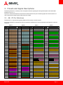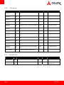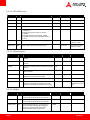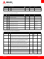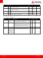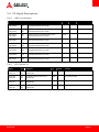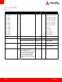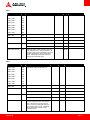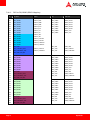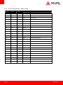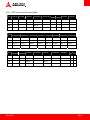
1
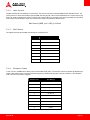
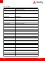
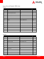
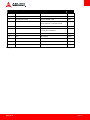
Express-HL User’s Manual Manual Revision: 0.10 Preliminary Revision Date: August 28, 2013 Part Number: 50- 1J046-1000 Revision History Revision Description Date By 0.10 Preliminary release 2013-08-28 JC Page 2 Express-IB Preface Copyright 2013 ADLINK Technology, Inc. This document contains proprietary information protected by copyright. All rights are reserved. No part of this manual may be reproduced by any mechanical, electronic, or other means in any form without prior written permission of the manufacturer. Disclaimer The information in this document is subject to change without prior notice in order to improve reliability, design, and function and does not represent a commitment on the part of the manufacturer. In no event will the manufacturer be liable for direct, indirect, special, incidental, or consequential damages arising out of the use or inability to use the product or documentation, even if advised of the possibility of such damages. Environmental Responsibility ADLINK is committed to fulfill its social responsibility to global environmental preservation through compliance with the European Union's Restriction of Hazardous Substances (RoHS) directive and Waste Electrical and Electronic Equipment (WEEE) directive. Environmental protection is a top priority for ADLINK. We have enforced measures to ensure that our products, manufacturing processes, components, and raw materials have as little impact on the environment as possible. When products are at their end of life, our customers are encouraged to dispose of them in accordance with the product disposal and/or recovery programs prescribed by their nation or company. Trademarks Product names mentioned herein are used for identification purposes only and may be trademarks and/or registered trademarks of their respective companies. Express-IB Page 3 Table of Contents Revision History ............................................................................................................ 2 Preface............................................................................................................................ 3 1. Introduction ......................................................................................................... 7 2. Specifications....................................................................................................... 8 2.1. Core System..............................................................................................................................8 2.2. Expansion Busses......................................................................................................................8 2.3. SEMA Board Controller.............................................................................................................8 2.4. Video.........................................................................................................................................8 2.5. Audio.........................................................................................................................................9 2.6. LAN ...........................................................................................................................................9 2.7. Multi I/O and Storage ...............................................................................................................9 2.8. TPM (Trusted Platform Module) ..............................................................................................9 2.9. Debug........................................................................................................................................9 2.10. Power Specifications ................................................................................................................9 2.11. Operating Temperatures ....................................................................................................... 10 2.12. Environmental ....................................................................................................................... 10 2.13. Specification Compliance ...................................................................................................... 10 2.14. Operating Systems................................................................................................................. 10 2.15. Specification Compliance ...................................................................................................... 10 2.16. Functional Diagram................................................................................................................ 11 2.17. Mechanical Drawing .............................................................................................................. 12 3. Page 4 Pinouts and Signal Descriptions...................................................................... 13 3.1. AB / CD Pin Definitions .......................................................................................................... 13 3.2. Signal Description Terminology............................................................................................. 16 3.3. AB Signal Descriptions ........................................................................................................... 17 3.3.1. Audio Signals....................................................................................................................................17 3.3.2. Analog VGA ......................................................................................................................................17 3.3.3. LVDS .................................................................................................................................................17 3.3.4. Gigabit Ethernet...............................................................................................................................18 3.3.5. Serial ATA .........................................................................................................................................19 3.3.6. PCI Express .......................................................................................................................................20 3.3.7. Express Card.....................................................................................................................................20 3.3.8. LPC bus.............................................................................................................................................21 3.3.9. USB...................................................................................................................................................21 Express-IB 3.3.10. SPI (BIOS only) .............................................................................................................................22 3.3.11. Miscellaneous..............................................................................................................................22 3.3.12. SMBus..........................................................................................................................................22 3.3.13. I2C Bus.........................................................................................................................................23 3.3.14. General Purpose I/O (GPIO) ........................................................................................................23 3.3.15. Power And System Management................................................................................................23 3.3.16. Power and Ground ......................................................................................................................24 3.4. CD Signal Descriptions ........................................................................................................... 25 3.4.1. USB 3.0 extension ............................................................................................................................25 3.4.2. PCI Express x1 ..................................................................................................................................25 3.4.3. DDI Channels....................................................................................................................................26 3.4.4. DDI to DP/HDMI/SDVO Mapping .....................................................................................................28 3.4.5. PCI Express Graphics x16 (PEG)........................................................................................................29 3.4.6. Module Type Definition ...................................................................................................................30 3.4.7. Power and Ground...........................................................................................................................30 4. Connector Pinouts on Module......................................................................... 31 4.1. 40-pin Multipurpose Connector ............................................................................................ 32 4.2. Status LEDs ............................................................................................................................ 34 4.3. XDP Debug header................................................................................................................. 35 4.4. Fan Connector ....................................................................................................................... 36 4.5. BIOS Setup Defaults RESET Switch ........................................................................................ 36 4.6. PCI Express Configuration Switch .......................................................................................... 36 4.7. PCIe x16-to-two-x8 Adapter Card.......................................................................................... 37 Smart Embedded Management Agent (SEMA) ............................................. 38 5. 5.1. Board Specific SEMA Functions ............................................................................................. 38 5.1.1. Voltages ...........................................................................................................................................38 5.1.2. Main Current....................................................................................................................................39 5.1.3. BMC Status.......................................................................................................................................39 5.1.4. Exception Codes...............................................................................................................................39 5.1.5. BMC Flags.........................................................................................................................................40 6. System Resources.............................................................................................. 41 6.1. System Memory Map ............................................................................................................ 41 6.2. Direct Memory Access Channels ........................................................................................... 41 6.3. I/O Map.................................................................................................................................. 42 6.4. Interrupt Request (IRQ) Lines................................................................................................ 44 6.5. PCI Configuration Space Map ................................................................................................ 46 6.6. PCI Interrupt Routing Map .................................................................................................... 47 Express-IB Page 5 Safety Instructions ...................................................................................................... 48 Getting Service ............................................................................................................ 49 Page 6 Express-IB 1. Introduction The Express-HL is a COM Express® COM.0 R2.1 Type 6 module supporting the 64-bit 4th Generation Intel® Core™ i7/i5/3 processor with CPU, memory controller, and graphics processor on the same chip. Based on the latest Mobile Intel® QM87 Express chipset, the ExpressHL is specifically designed for customers who need high-level processing and graphics performance in a long product life solution. The Express-HL features the Intel® Core™ i7/i5/i3 processor supporting Intel® Hyper-Threading Technology (up to 4 cores, 8 threads) and DDR3 dual-channel memory at 1333/1600 MHz to provide excellent overall performance. Intel® Flexible Display Interface and Direct Media Interface provide high speed connectivity to the Intel® QM77 Express chipset. Integrated Intel Generation 7.5 includes features such as OpenGL 3.1, DirectX11, Intel® Clear Video HD Technology, Advanced Scheduler 2.0, 1.0, XPDM support, and DirectX Video Acceleration (DXVA) support for full AVC/VC1/MPEG2 hardware decode. Graphics outputs include VGA, LVDS and three DDI ports supporting HDMI / DVI / DisplayPort or SDVO. The Express-HL is specifically designed for customers with high-performance processing graphics requirements who want to outsource the custom core logic of their systems for reduced development time. The Express-HL has dual stacked SODIMM sockets for up to 32 GB DDR3 memory. The Intel® Mobile QM87 Express chipset integrates VGA and dual-channel 18/24-bit LVDS display output. In addition to the onboard integrated graphics, a multiplexed PCI Express® x16 Graphics bus is available for discrete graphics expansion or general purpose x8 or x4 PCI Express® connectivity. The Express-HL features a single onboard Gigabit Ethernet port, four USB 3.0 ports and four USB 2.0 ports, and 4 SATA 6 Gb/s ports. Support is provided for SMBus and I2C. The module is equipped with SPI AMI EFI BIOS with CMOS backup, supporting embedded features such as remote console, CMOS backup, hardware monitor, and watchdog timer. Express-IB Page 7 2. Specifications 2.1. Core System ¾ CPU: 4th Generation Intel® Core™ i7 Processors (Mobile) - 22nm, also known as Haswell Platform • • • • • • • Intel® Core™ i7-4860EQ 2.4 GHz (3.2 GHz Turbo), 47W (4C/GT3) Intel® Core™ i7-4700EQ 2.4/1.7 GHz (3.4 GHz Turbo), 47/37W (4C/GT2) Intel® Core™ i5-4400E 2.7 GHz (3.3 GHz Turbo), 37W (2C/GT2) Intel® Core™ i5-4402E 1.6 GHz (2.7 GHz Turbo), 25W (2C/GT2) Intel® Core™ i3-4100E 2.4 GHz (no Turbo) 3MB, 37W (2C/GT2) Intel® Core™ i5-4102E 1.6 GHz (no Turbo) 3MB, 25W (2C/GT2) and Intel® Celeron ¾ L3 Cache: 6MB for i7-4650U, 3MB for i5-4400E, i5-4402E, i3-4100E and i3-4102E ¾ Memory: Dual channel non-ECC 1600/1333 MHz DDR3L memory up to 32GB in dual SODIMM socket ¾ Chipset: Mobile Intel® QM87 Express Chipset ¾ BIOS: AMI EFI with CMOS backup in 8MB SPI BIOS with Intel® AMT 9.0 support 2.2. Expansion Busses ¾ PCI Express x16 (Gen3) or PCI Express (2 x8 or 1 x8 with 2 x4) ¾ 6 PCI Express x1 (AB): Lanes 0/1/2/3/4/5 ¾ 1 PCI Express x1 (CD): Lane 6 ¾ LPC bus, SMBus (system) , I2C (user) 2.3. SEMA Board Controller ¾ Type: ADLINK Smart Embedded Management Agent (SEMA) ¾ Supports: • • • • • • • • Voltage/Current monitoring Power sequence debug support AT/ATX mode control Logistics and Forensic information Flat Panel Control General Purpose I2C Failsafe BIOS (dual BIOS ) Watchdog Timer and Fan Control 2.4. Video ¾ Integrated in Processor: Intel® Generation 7.5 graphics core architecture ¾ GPU Feature Support: • • • • • • • • • • Page 8 3 independent and simultaneous display combinations of DisplayPort /HDMI / LVDS monitors Encode/transcode HD content Playback of high definition content including Blu-ray Disc* Superior image quality with sharper, more colorful images Playback of Blu-ray* disc S3D content using HDMI (1.4a spec compliant with 3D) DirectX* Video Acceleration (DXVA) support for accelerating video processing Full AVC/VC1/MPEG2 HW Decode Advanced Scheduler 2.0, 1.0, XPDM support Windows* 8, Windows* 7, OSX, Linux* OS support DirectX* 11, DirectX* Express-IB ¾ Multi Display Support: 3 independent displays ¾ Display Types • • • VGA Interface support with 300 MHz DAC Analog monitor support up to QXGA (2048 x 1536) LVDS Interface single/dual channel 18/24-bit LVDS through eDP (two lane) to LVDS Realtek RTD2136R Digital Display Ports x3 DDI1 supporting DisplayPort / HDMI / DVI DDI2 supporting DisplayPort / HDMI / DVI DDI3 supporting DisplayPort / HDMI / DVI 2.5. Audio ¾ Integrated: Intel® HD Audio integrated in PCH QM87 ¾ Audio Codec: Realtek ALC886 on Express-BASE6 2.6. LAN ¾ Integrated: LAN MAC integrated in PCH QM87 ¾ Intel PHY: Intel® Ethernet Controller I217LM ¾ Interface: 10/100/1000 GbE connection 2.7. Multi I/O and Storage ¾ Integrated in Intel® QM87 Express Chipset ¾ USB ports: 4 ports USB 3.0 (USB0,1,2,3) and 4 ports USB 2.0 (USB4,5,6,7) ¾ SATA ports: four ports SATA 6Gb/s (SATA0, SATA1, SATA2, SATA3) ¾ Serial: 2 UART ports COM1/2 with console redirection ¾ GPIO: 4 GPO and 4 GPI with interrupt 2.8. TPM (Trusted Platform Module) ¾ Chipset: ATMEL AT97SC3204 ¾ Type: TPM 1.2 ¾ Optional: TPM is qualified during design but is an option in production 2.9. Debug ¾ 40-pin multipurpose flat cable connector to be used with DB-40 debug module • ¾ supports : BIOS POSTCODE LED, BMC access, SPI BIOS flashing, Power Testpoints, Debug LEDs 60-pin XDP header for ICE debug of CPU/Chipset 2.10. Power Specifications ¾ Power Modes: ¾ Standard Voltage Input: ATX = 12V±5% / 5Vsb ±5% or AT = 12V ±5% ¾ Wide Voltage Input: ATX = 5~20 V / 5Vsb ±5% or AT = 5 ~20V ¾ Power Management: ACPI 4.0 compliant, Smart Battery support ¾ Power States: supports C1-C6, S0, S1, S4, S3, S5, S5 ECO mode (Wake on USB S3/S4, WOL S3/S4/S5) Express-IB AT and ATX mode (AT mode start controlled by SEMA) Page 9 2.11. Operating Temperatures ¾ Standard Operating Temperature: 0 to 60°C (Wide Voltage Input) ¾ Industrial Operating Temperature: -20 to 70°C (Wide Voltage Input) ¾ Extreme Rugged Operating Temperature: -40 to 85°C (Standard Voltage Input) 2.12. Environmental ¾ Humidity: 5-90% RH operating, non-condensing 5-95% RH storage (and operating with conformal coating). ¾ Shock and Vibration: IEC 60068-2-64 and IEC-60068-2-27 MIL-STD-202F, Method 213B, Table 213-I, Condition A and Method 214A, Table 214-I, Condition D ¾ Halt: Thermal Stress, Vibration Stress, Thermal Shock and Combined Test 2.13. Specification Compliance ¾ PICMG COM.0: Rev 2.1 Type 6, basic size 125 x 95 2.14. Operating Systems ¾ Standard Support: Windows 7/8 32/64-bit, Linux 32/64-bit ¾ Extended Support (BSP): WEC7/8, Linux , VxWorks 2.15. Specification Compliance ¾ PICMG COM.0: Rev 2.1 Type 6, basic size 125 x 95 Page 10 Express-IB Express-IB DMI CD AB FDI 2.16. Functional Diagram Page 11 2.17. Mechanical Drawing Page 12 Express-IB 3. Pinouts and Signal Descriptions The following information is a summary of the most important information regarding pinout and signal description in the official PICMG COM.0 Rev 2.0 (soon 2.1) The pinout is noted here to emphazise issues that have not been followed in the past. The following might have small inacuaracies so in case of doubt the offical design guide of PICMG should be consulted. 3.1. AB / CD Pin Definitions The Express-HL is a Type 6 module supporting USB3.0 and DDI channels on the CD connector All pin in the specification are described also those not supported on the Express-HL. Those not supported on the Express-HL module are crossed out Row A Row B Row C Row D Pin Name Pin Name Pin Name Pin Name A1 GND (FIXED) B1 GND (FIXED) C1 GND FIXED) D1 GND FIXED) A2 GBE0_MDI3- B2 GBE0_ACT# C2 GND D2 GND A3 GBE0_MDI3+ B3 LPC_FRAME# C3 USB_SSRX0- D3 USB_SSTX0- A4 GBE0_LINK100# B4 LPC_AD0 C4 USB_SSRX0+ D4 USB_SSTX0+ A5 GBE0_LINK1000# B5 LPC_AD1 C5 GND D5 GND A6 GBE0_MDI2- B6 LPC_AD2 C6 USB_SSRX1- D6 USB_SSTX1- A7 GBE0_MDI2+ B7 LPC_AD3 C7 USB_SSRX1+ D7 USB_SSTX1+ A8 GBE0_LINK# B8 LPC_DRQ0# C8 GND D8 GND A9 GBE0_MDI1- B9 LPC_DRQ1# C9 USB_SSRX2- D9 USB_SSTX2- A10 GBE0_MDI1+ B10 LPC_CLK C10 USB_SSRX2+ D10 USB_SSTX2+ A11 GND (FIXED) B11 GND (FIXED) C11 GND (FIXED) D11 GND (FIXED) A12 GBE0_MDI0- B12 PWRBTN# C12 USB_SSRX3- D12 USB_SSTX3- A13 GBE0_MDI0+ B13 SMB_CK C13 USB_SSRX3+ D13 USB_SSTX3+ A14 GBE0_CTREF B14 SMB_DAT C14 GND D14 GND A15 SUS_S3# B15 SMB_ALERT# C15 DDI1_PAIR6+ D15 DDI1_CTRLCLK_AUX+ A16 SATA0_TX+ B16 SATA1_TX+ C16 DDI1_PAIR6- D16 DDI1_CTRLDATA_AUX A17 SATA0_TX- B17 SATA1_TX- C17 RSVD D17 RSVD A18 SUS_S4# B18 SUS_STAT# C18 RSVD D18 RSVD A19 SATA0_RX+ B19 SATA1_RX+ C19 PCIE_RX6+ D19 PCIE_TX6+ A20 SATA0_RX- B20 SATA1_RX- C20 PCIE_RX6- D20 PCIE_TX6- A21 GND (FIXED) B21 GND (FIXED) C21 GND (FIXED) D21 GND (FIXED) A22 SATA2_TX+ B22 SATA3_TX+ C22 PCIE_RX7+ D22 PCIE_TX7+ A23 SATA2_TX- B23 SATA3_TX- C23 PCIE_RX7- D23 PCIE_TX7- A24 SUS_S5# B24 PWR_OK C24 DDI1_HPD D24 RSVD A25 SATA2_RX+ B25 SATA3_RX+ C25 DDI1_PAIR4+ D25 RSVD A26 SATA2_RX- B26 SATA3_RX- C26 DDI1_PAIR4- D26 DDI1_PAIR0+ A27 BATLOW# B27 WDT C27 RSVD D27 DDI1_PAIR0- A28 (S)ATA_ACT# B28 AC/HDA_SDIN2 C28 RSVD D28 RSVD A29 AC/HDA_SYNC B29 AC/HDA_SDIN1 C29 DDI1_PAIR5+ D29 DDI1_PAIR1+ A30 AC/HDA_RST# B30 AC/HDA_SDIN0 C30 DDI1_PAIR5- D30 DDI1_PAIR1- A31 GND (FIXED) B31 GND (FIXED) C31 GND (FIXED) D31 GND (FIXED) A32 AC/HDA_BITCLK B32 SPKR C32 DDI2_CTRLCLK_AUX+ D32 DDI1_PAIR2+ A33 AC/HDA_SDOUT B33 I2C_CK C33 DDI2_CTRLDATA_AUX- D33 DDI1_PAIR2- A34 BIOS_DIS0# B34 I2C_DAT C34 DDI2_DDC_AUX_SEL D34 DDI1_DDC_AUX_SEL A35 THRMTRIP# B35 THRM# C35 RSVD D35 RSVD Express-IB Page 13 Row A Row B Row C Row D Pin Name Pin Name Pin Name Pin Name A36 USB6- B36 USB7- C36 DDI3_CTRLCLK_AUX+ D36 DDI1_PAIR3+ A37 USB6+ B37 USB7+ C37 DDI3_CTRLDATA_AUX- D37 DDI1_PAIR3- A38 USB_6_7_OC# B38 USB_4_5_OC# C38 DDI3_DDC_AUX_SEL D38 RSVD A39 USB4- B39 USB5- C39 DDI3_PAIR0+ D39 DDI2_PAIR0+ A40 USB4+ B40 USB5+ C40 DDI3_PAIR0- D40 DDI2_PAIR0- A41 GND (FIXED) B41 GND (FIXED) C41 GND (FIXED) D41 GND (FIXED) A42 USB2- B42 USB3- C42 DDI3_PAIR1+ D42 DDI2_PAIR1+ A43 USB2+ B43 USB3+ C43 DDI3_PAIR1- D43 DDI2_PAIR1- A44 USB_2_3_OC# B44 USB_0_1_OC# C44 DDI3_HPD D44 DDI2_HPD A45 USB0- B45 USB1- C45 RSVD D45 RSVD A46 USB0+ B46 USB1+ C46 DDI3_PAIR2+ D46 DDI2_PAIR2+ A47 VCC_RTC B47 EXCD1_PERST# C47 DDI3_PAIR2- D47 DDI2_PAIR2- A48 EXCD0_PERST# B48 EXCD1_CPPE# C48 RSVD D48 RSVD A49 EXCD0_CPPE# B49 SYS_RESET# C49 DDI3_PAIR3+ D49 DDI2_PAIR3+ A50 LPC_SERIRQ B50 CB_RESET# C50 DDI3_PAIR3- D50 DDI2_PAIR3- A51 GND (FIXED) B51 GND (FIXED) C51 GND (FIXED) D51 GND (FIXED) A52 PCIE_TX5+ B52 PCIE_RX5+ C52 PEG_RX0+ D52 PEG_TX0+ A53 PCIE_TX5- B53 PCIE_RX5- C53 PEG_RX0- D53 PEG_TX0- A54 GPI0 B54 GPO1 C54 TYPE0# D54 PEG_LANE_RV# A55 PCIE_TX4+ B55 PCIE_RX4+ C55 PEG_RX1+ D55 PEG_TX1+ A56 PCIE_TX4- B56 PCIE_RX4- C56 PEG_RX1- D56 PEG_TX1- A57 GND B57 GPO2 C57 TYPE1# D57 TYPE2# A58 PCIE_TX3+ B58 PCIE_RX3+ C58 PEG_RX2+ D58 PEG_TX2+ A59 PCIE_TX3- B59 PCIE_RX3- C59 PEG_RX2- D59 PEG_TX2- A60 GND (FIXED) B60 GND (FIXED) C60 GND (FIXED) D60 GND (FIXED) A61 PCIE_TX2+ B61 PCIE_RX2+ C61 PEG_RX3+ D61 PEG_TX3+ A62 PCIE_TX2- B62 PCIE_RX2- C62 PEG_RX3- D62 PEG_TX3- A63 GPI1 B63 GPO3 C63 RSVD D63 RSVD A64 PCIE_TX1+ B64 PCIE_RX1+ C64 RSVD D64 RSVD A65 PCIE_TX1- B65 PCIE_RX1- C65 PEG_RX4+ D65 PEG_TX4+ A66 GND B66 WAKE0# C66 PEG_RX4- D66 PEG_TX4- A67 GPI2 B67 WAKE1# C67 RSVD D67 GND A68 PCIE_TX0+ B68 PCIE_RX0+ C68 PEG_RX5+ D68 PEG_TX5+ A69 PCIE_TX0- B69 PCIE_RX0- C69 PEG_RX5- D69 PEG_TX5- A70 GND (FIXED) B70 GND (FIXED) C70 GND (FIXED) D70 GND (FIXED) A71 LVDS_A0+ B71 LVDS_B0+ C71 PEG_RX6+ D71 PEG_TX6+ A72 LVDS_A0- B72 LVDS_B0- C72 PEG_RX6- D72 PEG_TX6- A73 LVDS_A1+ B73 LVDS_B1+ C73 GND D73 GND A74 LVDS_A1- B74 LVDS_B1- C74 PEG_RX7+ D74 PEG_TX7+ A75 LVDS_A2+ B75 LVDS_B2+ C75 PEG_RX7- D75 PEG_TX7- A76 LVDS_A2- B76 LVDS_B2- C76 GND D76 GND A77 LVDS_VDD_EN B77 LVDS_B3+ C77 RSVD D77 RSVD A78 LVDS_A3+ B78 LVDS_B3- C78 PEG_RX8+ D78 PEG_TX8+ A79 LVDS_A3- B79 LVDS_BKLT_EN C79 PEG_RX8- D79 PEG_TX8- A80 GND (FIXED) B80 GND (FIXED) C80 GND (FIXED) D80 GND (FIXED) Page 14 Express-IB Row A Row B Row C Row D Pin Name Pin Name Pin Name Pin Name A81 LVDS_A_CK+ B81 LVDS_B_CK+ C81 PEG_RX9+ D81 PEG_TX9+ A82 LVDS_A_CK- B82 LVDS_B_CK- C82 PEG_RX9- D82 PEG_TX9- A83 LVDS_I2C_CK B83 LVDS_BKLT_CTRL C83 TPM_PP D83 RSVD A84 LVDS_I2C_DAT B84 VCC_5V_SBY C84 GND D84 GND A85 GPI3 B85 VCC_5V_SBY C85 PEG_RX10+ D85 PEG_TX10+ A86 RSVD B86 VCC_5V_SBY C86 PEG_RX10- D86 PEG_TX10- A87 RSVD B87 VCC_5V_SBY C87 GND D87 GND A88 PCIE0_CK_REF+ B88 BIOS_DIS1# C88 PEG_RX11+ D88 PEG_TX11+ A89 PCIE0_CK_REF- B89 VGA_RED C89 PEG_RX11- D89 PEG_TX11- A90 GND (FIXED) B90 GND (FIXED) C90 GND (FIXED) D90 GND (FIXED) A91 SPI_POWER B91 VGA_GRN C91 PEG_RX12+ D91 PEG_TX12+ A92 SPI_MISO B92 VGA_BLU C92 PEG_RX12- D92 PEG_TX12- A93 GPO0 B93 VGA_HSYNC C93 GND D93 GND A94 SPI_CLK B94 VGA_VSYNC C94 PEG_RX13+ D94 PEG_TX13+ A95 SPI_MOSI B95 VGA_I2C_CK C95 PEG_RX13- D95 PEG_TX13- A96 TPM_PP B96 VGA_I2C_DAT C96 GND D96 GND A97 TYPE10# B97 SPI_CS# C97 RSVD D97 RSVD A98 SER0_TX B98 RSVD C98 PEG_RX14+ D98 PEG_TX14+ A99 SER0_RX B99 RSVD C99 PEG_RX14- D99 PEG_TX14- A100 GND (FIXED) B100 GND (FIXED) C100 GND (FIXED) D100 GND (FIXED) A101 SER1_TX B101 FAN_PWMOUT C101 PEG_RX15+ D101 PEG_TX15+ A102 SER1_RX B102 FAN_TACHIN C102 PEG_RX15- D102 PEG_TX15- A103 LID# B103 SLEEP# C103 GND D103 GND A104 VCC_12V B104 VCC_12V C104 VCC_12V D104 VCC_12V A105 VCC_12V B105 VCC_12V C105 VCC_12V D105 VCC_12V A106 VCC_12V B106 VCC_12V C106 VCC_12V D106 VCC_12V A107 VCC_12V B107 VCC_12V C107 VCC_12V D107 VCC_12V A108 VCC_12V B108 VCC_12V C108 VCC_12V D108 VCC_12V A109 VCC_12V B109 VCC_12V C109 VCC_12V D109 VCC_12V A110 GND (FIXED) B110 GND (FIXED) C110 GND (FIXED) D110 GND (FIXED) Express-IB Page 15 3.2. Signal Description Terminology The following terms are used in the COM Express AB/CD Signal Descriptions below. Page 16 I Input to the Module O Output from the Module I/O Bi-directional input / output signal OD Open drain output I 3.3V Input 3.3V tolerant I 5V Input 5V tolerant O 3.3V Output 3.3V signal level O 5V Output 5V signal level I/O 3.3V Bi-directional signal 3.3V tolerant I/O 5V Bi-directional signal 5V tolerant I/O 3.3Vsb Input 3.3V tolerant active in standby state P Power Input/Output REF Reference voltage output that may be sourced from a module power plane. PDS Pull-down strap. This is an output pin on the module that is either tied to GND or not connected. The signal is used to indicate the PICMG module type to the Carrier Board. PU ADLINK implemented pull-up resistor on module PD ADLINK implemented pull-down resistor on module Express-IB 3.3. AB Signal Descriptions 3.3.1. Audio Signals Signal Pin # Description I/O AC_RST# / HDA_RST# A30 Reset output to CODEC, active low. O 3.3VSB AC_SYNC / HDA_SYNC A29 Sample-synchronization signal to the CODEC(s). O 3.3V AC_BITCLK / HDA_BITCLK A32 Serial data clock generated by the external CODEC(s). I/O 3.3V AC _SDOUT / HDA_SDOUT A33 Serial TDM data output to the CODEC. O 3.3V AC _SDIN[2:0] HDA_SDIN[2:0] B28 B30 Serial TDM data inputs from up to 3 CODECs. I/O 3.3VSB 3.3.2. PU/PD Comment Analog VGA Signal Pin # Description I/O VGA_RED B89 Red for monitor. Analog DAC output, designed to drive a 37.5-Ohm equivalent load. O Analog If VGA is used than signal should be pulled to GND by 150Ω on the carrier VGA_GRN B91 Green for monitor Analog DAC output, designed to drive a 37.5-Ohm equivalent load. O Analog If VGA is used than signal should be pulled to GND by 150Ω on the carrier VGA_BLU B92 Blue for monitor. Analog DAC output, designed to drive a 37.5-Ohm equivalent load. O Analog If VGA is used than signal should be pulled to GND by 150Ω on the carrier VGA_HSYNC B93 Horizontal sync output to VGA monitor O 3.3V VGA_VSYNC B94 Vertical sync output to VGA monitor O 3.3V VGA_I2C_CK B95 DDC clock line (I²C port dedicated to identify VGA monitor capabilities) I/O OD 3.3V PU 2k2 3.3V VGA_I2C_DAT B96 DDC data line. I/O OD 3.3V PU 2k2 3.3V 3.3.3. PU/PD LVDS Signal Pin # Description I/O LVDS_A0+ LVDS_A0LVDS_A1+ LVDS_A1LVDS_A2+ LVDS_A2LVDS_A3+ LVDS_A3- A71 A72 A73 A74 A75 A76 A78 A79 LVDS Channel A differential pairs O LVDS LVDS_A_CK+ LVDS_A_CK- A81 A82 LVDS Channel A differential clock O LVDS LVDS_B0+ B71 LVDS Channel B differential pairs O LVDS Express-IB Comment PU/PD Comment Page 17 Signal Pin # Description I/O LVDS_B0LVDS_B1+ LVDS_B1LVDS_B2+ LVDS_B2LVDS_B3+ LVDS_B3- B72 B73 B74 B75 B76 B77 B78 LVDS_B_CK+ LVDS_B_CK- B81 B82 LVDS Channel B differential clock O LVDS LVDS_VDD_EN A77 LVDS panel power enable O 3.3V LVDS_BKLT_EN B79 LVDS panel backlight enable O 3.3V LVDS_BKLT_CTRL B83 LVDS panel backlight brightness control O 3.3V LVDS_I2C_CK A83 DDC lines used for flat panel detection and control. O 3.3V PU 2k2 3.3V LVDS_I2C_DAT A84 DDC lines used for flat panel detection and control. I/O 3.3V PU 2k2 3.3V 3.3.4. PU/PD Gigabit Ethernet Gigabit Ethernet Pin # Description I/O GBE0_MDI0+ GBE0_MDI0GBE0_MDI1+ GBE0_MDI1GBE0_MDI2+ GBE0_MDI2GBE0_MDI3+ GBE0_MDI3- A13 A11 A10 A9 A7 A6 A3 A2 Gigabit Ethernet Controller 0: Media Dependent Interface Differential Pairs 0, 1, 2, 3. The MDI can operate in 1000, 100, and 10Mbit/sec modes. Some pairs are unused in some modes according to the following: I/O Analog GBE0_ACT# B2 Gigabit Ethernet Controller 0 activity indicator, active low. O 3.3VSB GBE0_LINK# A8 Gigabit Ethernet Controller 0 link indicator, active low. O 3.3VSB GBE0_LINK100# A4 Gigabit Ethernet Controller 0 100Mbit/sec link indicator, active low. O 3.3VSB GBE0_LINK1000# A5 Gigabit Ethernet Controller 0 1000Mbit/sec link indicator, active low. O 3.3VSB GBE0_CTREF A14 Reference voltage for Carrier Board Ethernet channel 1 and 2 magnetics center tap. The reference voltage is determined by the requirements of the Module PHY and may be as low as 0V and as high as 3.3V. The reference voltage output shall be current limited on the Module. In the case in which the reference is shorted to ground, the current shall be 250 mA or less. GND min 3.3V max Page 18 Comment MDI[0]+/MDI[1]+/MDI[2]+/MDI[3]+/- 1000BASE-T B1_DA+/B1_DB+/B1_DC+/B1_DD+/- 100BASE-TX TX+/RX+/- PU/PD Comment Twisted pair signals for external transformer. 10BASE-T TX+/RX+/- Express-IB 3.3.5. Serial ATA Signal Pin # Description I/O SATA0_TX+ SATA0_TX- A16 A17 Serial ATA channel 0, Transmit Output differential pair. O SATA AC coupled on Module SATA0_RX+ SATA0_RX- A19 A20 Serial ATA channel 0, Receive Input differential pair. I SATA AC coupled on Module SATA1_TX+ SATA1_TX- B16 B17 Serial ATA channel 1, Transmit Output differential pair. O SATA AC coupled on Module SATA1_RX+ SATA1_RX- B19 B20 Serial ATA channel 1, Receive Input differential pair. I SATA AC coupled on Module SATA2_TX+ SATA2_TX- A22 A23 Serial ATA channel 2, Transmit Output differential pair. O SATA AC coupled on Module SATA2_RX+ SATA2_RX- A25 A26 Serial ATA channel 2, Receive Input differential pair. I SATA AC coupled on Module SATA3_TX+ SATA3_TX- B22 B23 Serial ATA channel 3, Transmit Output differential pair. O SATA AC coupled on Module SATA3_RX+ SATA3_RX- B25 B26 Serial ATA channel 3, Receive Input differential pair. I SATA AC coupled on Module (S)ATA_ACT# A28 ATA (parallel and serial) or SAS activity indicator, active low. O 3.3V Express-IB PU/PD Comment Page 19 3.3.6. PCI Express Signal Pin # Description I/O PCIE_TX0+ PCIE_TX0- A68 A69 PCI Express channel 0, Transmit Output differential pair. O PCIE AC coupled on Module PCIE_RX0+ PCIE_RX0- B68 B69 PCI Express channel 0, Receive Input differential pair. I PCIE AC coupled off Module PCIE_TX1+ PCIE_TX1- A64 A65 PCI Express channel 1, Transmit Output differential pair. O PCIE AC coupled on Module PCIE_RX1+ PCIE_RX1- B64 B65 PCI Express channel 1, Receive Input differential pair. I PCIE AC coupled off Module PCIE_TX2+ PCIE_TX2- A61 A62 PCI Express channel 2, Transmit Output differential pair. O PCIE AC coupled on Module PCIE_RX2+ PCIE_RX2- B61 B62 PCI Express channel 2, Receive Input differential pair. I PCIE AC coupled off Module PCIE_TX3+ PCIE_TX3- A58 A59 PCI Express channel 3, Transmit Output differential pair. O PCIE AC coupled on Module PCIE_RX3+ PCIE_RX3- B58 B59 PCI Express channel 3, Receive Input differential pair. I PCIE AC coupled off Module PCIE_TX4+ PCIE_TX4- A55 A56 PCI Express channel 4, Transmit Output differential pair. O PCIE AC coupled on Module PCIE_RX4+ PCIE_RX4- B55 B56 PCI Express channel 4, Receive Input differential pair. I PCIE AC coupled off Module PCIE_TX5+ PCIE_TX5- A52 A53 PCI Express channel 5, Transmit Output differential pair. O PCIE AC coupled on Module PCIE_RX5+ PCIE_RX5- B52 B53 PCI Express channel 5, Receive Input differential pair. I PCIE AC coupled off Module PCIE_CLK_REF+ PCIE_CLK_REF- A88 A89 PCI Express Reference Clock output for all PCI Express and PCI Express Graphics Lanes. O PCIE 3.3.7. PU/PD Express Card Signal Pin # Description I/O PU/PD EXCD0_CPPE# EXCD1_CPPE# A49 B48 PCI ExpressCard: PCI Express capable card request I 3.3V PU 10k 3.3V EXCD0_PERST# EXCD1_PERST# A48 B47 PCI ExpressCard: reset O 3.3V Page 20 Comment Comment Cannot be tested on ExpressBASE6 (DVT issue) Express-IB 3.3.8. LPC bus Signal Pin # Description I/O LPC_AD[0:3] B4-B7 LPC multiplexed address, command and data bus I/O 3.3V LPC_FRAME# B3 LPC frame indicates the start of an LPC cycle O 3.3V LPC_DRQ0# LPC_DRQ1# B8 B9 LPC serial DMA request I 3.3V LPC_SERIRQ A50 LPC serial interrupt I/O OD 3.3V LPC_CLK B10 LPC clock output - 33MHz nominal O 3.3V 3.3.9. PU/PD Comment PU 8k2 3.3V USB Signal Pin # Description I/O USB0+ USB0- A46 A45 USB differential data pairs for Port 0 I/O 3.3VSB USB 1.1/ 2.0 compliant USB1+ USB1- B46 B45 USB differential data pairs for Port 1 I/O 3.3VSB USB 1.1/ 2.0 compliant USB2+ USB2- A43 A42 USB differential data pairs for Port 1 I/O 3.3VSB USB 1.1/ 2.0 compliant USB3+ USB3- B43 B42 USB differential data pairs for Port 2 I/O 3.3VSB USB 1.1/ 2.0 compliant USB4+ USB4- A40 A39 USB differential data pairs for Port 3 I/O 3.3VSB USB 1.1/ 2.0 compliant USB5+ USB5- B40 B39 USB differential data pairs for Port 4 I/O 3.3VSB USB 1.1/ 2.0 compliant USB6+ USB6- A37 A36 USB differential data pairs for Port 5 I/O 3.3VSB USB 1.1/ 2.0 compliant USB7+ USB7- B37 B37 USB differential data pairs for Port 6 I/O 3.3VSB USB 1.1/ 2.0 compliant USB_0_1_OC# B44 USB over-current sense, USB ports 0 and 1. A pull-up for this line shall be present on the module. An open drain driver from a USB current monitor on the carrier board may drive this line low. I 3.3VSB PU 10k 3.3VSB Do not pull high on carrier USB_2_3_OC# A44 USB over-current sense, USB ports 2 and 3. A pull-up for this line shall be present on the module. An open drain driver from a USB current monitor on the carrier board may drive this line low. . I 3.3VSB PU 10k 3.3VSB Do not pull high on carrier USB_4_5_OC# B38 USB over-current sense, USB ports 4 and 5. A pull-up for this line shall be present on the module. An open drain driver from a USB current monitor on the carrier board may drive this line low. I 3.3VSB PU 10k 3.3VSB Do not pull high on carrier USB_6_7_OC# A38 USB over-current sense, USB ports 6 and 7. A pull-up for this line shall be present on the module. An open drain driver from a USB current monitor on the carrier board may drive this line low. I 3.3VSB PU 10k 3.3VSB Do not pull high on carrier Express-IB PU/PD Comment Page 21 3.3.10. SPI (BIOS only) Signal Pin # Description I/O PU/PD Comment SPI_CS# B97 Chip select for Carrier Board SPI BIOS Flash. O 3.3VSB SPI_MISO A92 Data in to module from carrier board SPI BIOS flash. I 3.3VSB SPI_MOSI A95 Data out from module to carrier board SPI BIOS flash. O 3.3VSB SPI_CLK A94 Clock from module to carrier board SPI BIOS flash. O 3.3VSB SPI_POWER A91 Power supply for Carrier Board SPI – sourced from Module – nominally 3.3V. The Module shall provide a minimum of 100mA on SPI_POWER. Carriers shall use less than 100mA of SPI_POWER. SPI_POWER shall only be used to power SPI devices on the Carrier O P 3.3VSB BIOS_DIS0# A34 Selection strap to determine the BIOS boot device. I PU 10K 3.3V Carrier shall pull to GND or leave no- connect. BIOS_DIS1# B88 Selection strap to determine the BIOS boot device. I PU 10K 3.3V Carrier shall pull to GND or leave no- connect 3.3.11. Miscellaneous Signal Pin # Description I/O PU/PD SPKR B32 Output for audio enunciator, the “speaker” in PC-AT systems O 3.3V WDT B27 Output indicating that a watchdog time-out event has occurred. O 3.3V THRM# B35 Input from off-module temp sensor indicating an over-temp situation. I 3.3V THERMTRIP# A35 Active low output indicating that the CPU has entered thermal shutdown. O 3.3V FAN_PWMOUT B101 Fan speed control. Uses the Pulse Width Modulation (PWM) technique to control the fan’s RPM. O OD 3.3V FAN_TACHIN11 B102 Fan tachometer input for a fan with a two pulse output. I OD 3.3V PU 10k 3.3V TPM_PP11 C83 Trusted Platform Module (TPM) Physical Presence pin. Active high. TPM chip has an internal pull down. This signal is used to indicate Physical Presence to the TPM. I 3.3V PD 3.3V Comment If TPM not installed on module than remove PD 3.3V 3.3.12. SMBus Signal Pin # Description I/O PU/PD SMB_CK B13 System Management Bus bidirectional clock line. Power sourced through 5V standby rail and main power rails. I/O OD 3.3VSB PU 2k2 3.3VSB SMB_DAT# B14 System Management Bus bidirectional data line. Power sourced through 5V standby rail and main power rails. I/O OD 3.3VSB PU 2k2 3.3VSB SMB_ALERT# B15 System Management Bus Alert – active low input can be used to generate an SMI# (System Management Interrupt) or to wake the system. Power sourced through 5V standby rail and main power rails. I 3.3VSB Page 22 Comment Express-IB 3.3.13. I2C Bus Signal Pin # Description I/O PU/PD Comment I2C_CK B33 General purpose I²C port clock output/input I/O OD 3.3VSB PU 2k2 3.3VSB I2C_DAT B34 General purpose I²C port data I/O line I/O OD 3.3VSB PU 2k2 3.3VSB PU/PD Comment 3.3.14. General Purpose I/O (GPIO) Signal Pin # Description I/O GPO[0] A93 General purpose output pins. O 3.3V GPO[1] B54 General purpose output pins. O 3.3V GPO[2] B57 General purpose output pins. O 3.3V GPO[3] B63 General purpose output pins. O 3.3V GPI[0] A54 General purpose input pins. Pulled high internally on the module. I 3.3V PU 10K 3.3V PU not in PICMG suggest 10K GPI[1] A63 General purpose input pins. Pulled high internally on the module. I 3.3V PU 10K 3.3V PU not in PICMG suggest 10K GPI[2] A67 General purpose input pins. Pulled high internally on the module. I 3.3V PU 10K 3.3V PU not in PICMG suggest 10K GPI[3] A85 General purpose input pins. Pulled high internally on the module. I 3.3V PU 10K 3.3V PU not in PICMG suggest 10K 3.3.15. Power And System Management Signal Pin # Description I/O PU/PD PWRBTN# B12 Power button to bring system out of S5 (soft off), active on falling edge. I 3.3VSB PU 10k 3.3VSB SYS_RESET# B49 Reset button input. Active low request for module to reset and reboot. May be falling edge sensitive. For situations when SYS_RESET# is not able to reestablish control of the system, PWR_OK or a power cycle may be used. I 3.3VSB PU 10k 3.3VSB CB_RESET# B50 Reset output from module to Carrier Board. Active low. Issued by module chipset and may result from a low SYS_RESET# input, a low PWR_OK input, a VCC_12V power input that falls below the minimum specification, a watchdog timeout, or may be initiated by the module software. O 3.3VSB PWR_OK B24 Power OK from main power supply. A high value indicates that the power is good. This signal can be used to hold off Module startup to allow carrier based FPGAs or other configurable devices time to be programmed. I 3.3V SUS_STAT# B18 Indicates imminent suspend operation; used to notify LPC devices. O 3.3VSB SUS_S3# A15 Indicates system is in Suspend to RAM state. Active-low output. An inverted copy of SUS_S3# on the carrier board (also known as “PS_ON”) may be used to enable the non-standby power on a typical ATX power supply. O 3.3VSB SUS_S4# A18 Indicates system is in Suspend to Disk state. Active low output. O 3.3VSB SUS_S5# A24 Indicates system is in Soft Off state. O 3.3VSB WAKE0# B66 PCI Express wake up signal. I 3.3VSB Express-IB TBD by R&D in CPLD Comment Should have weak pull up PU 10k 3.3VSB Page 23 Signal Pin # Description I/O PU/PD WAKE1# B67 General purpose wake up signal. May be used to implement wake-up on PS/2 keyboard or mouse activity. I 3.3VSB PU 10k 3.3VSB BATLOW# A27 Battery low input. This signal may be driven low by external circuitry to signal that the system battery is low, or may be used to signal some other external power-management event. I 3.3VSB PU 10k 3.3VSB LID# LID button. Low active signal used by the ACPI operating system for a LID switch. I OD 3.3VSB PU 10k 3.3VSB SLEEP# Sleep button. Low active signal used by the ACPI operating system to bring the system to sleep state or to wake it up again. I OD 3.3VSB PU 10K 3.3VSB Comment 3.3.16. Power and Ground Signal Pin # Description I/O VCC_12V A104-A109 Primary power input: +12V nominal (5 ~ 19V). See section 7 “Electrical Specifications“ for allowable input range. All available VCC_12V pins on the connector(s) shall be used. P B104-B109 VCC_5V_SBY B84-B87 Standby power input: +5.0V nominal. See section 7 “Electrical P Specifications“ for allowable input range. If VCC5_SBY is used, all available VCC_5V_SBY pins on the connector(s) shall be used. Only used for standby and suspend functions. May be left unconnected if these functions are not used in the system design. VCC_RTC A47 Real-time clock circuit-power input. Nominally +3.0V. GND A1, A11, A21, A31, Ground - DC power and signal and AC signal return path. A41, A51, A57, A66, A80, A90, A96, A100, A110, B1, B11, B21 ,B31, B41, B51, B60, B70, B80, B90, B100, B110 Page 24 PU/PD Comment 8.5~19 V 5Vsb ±5% P P Express-IB 3.4. CD Signal Descriptions 3.4.1. USB 3.0 extension Signal Pin Description I/O USB_SSRX0USB_SSRX0+ C3 C4 Additional Receive signal differential pairs for the SuperSpeed USB data path on USB0 I PCIE USB_SSTX0USB_SSTX0+ D3 D4 Additional Transmit signal differential pairs for the SuperSpeed USB data path on USB0 O PCIE USB_SSRX1USB_SSRX1+ C6 C7 Additional Receive signal differential pairs for the SuperSpeed USB data path on USB1 I PCIE USB_SSTX1USB_SSTX1+ D6 D7 Additional Transmit signal differential pairs for the SuperSpeed USB data path on USB1 O PCIE USB_SSRX2USB_SSRX2+ C9 C10 Additional Receive signal differential pairs for the SuperSpeed USB data path on USB2 I PCIE USB_SSTX2USB_SSTX2+ D9 D10 Additional Transmit signal differential pairs for the SuperSpeed USB data path on USB2 O PCIE USB_SSRX3USB_SSRX3+ C12 C13 Additional Receive signal differential pairs for the SuperSpeed USB data path on USB3 I PCIE USB_SSTX3USB_SSTX3+ D12 D13 Additional Transmit signal differential pairs for the SuperSpeed USB data path on USB3 O PCIE 3.4.2. PU/PD Comment AC coupled on Module AC coupled on Module AC coupled on Module AC coupled on Module PCI Express x1 Signal Pin # Description I/O PCIE_TX6+ PCIE_TX6- D19 D20 PCI Express channel 6, Transmit Output differential pair. O PCIE AC coupled on Module PCIE_RX6+ PCIE_RX6- C19 C20 PCI Express channel 6, Receive Input differential pair. I PCIE AC coupled off Module PCIE_TX7+ PCIE_TX7- D22 D23 PCI Express channel 7, Transmit Output differential pair. O PCIE Not available used by LAN PCIE_RX7+ PCIE_RX7- C22 C23 PCI Express channel 7, Receive Input differential pair. I PCIE Not available used by LAN Express-IB PU/PD Comment Page 25 3.4.3. DDI Channels DDI 1 Signal Pin Description I/O DDI1_PAIR0+ D26 Digital Display Interface1 differential pairs O PCIE DDI1_PAIR0- D27 SDVO1_RED- (AC coupled) DDI1_PAIR1+ D29 SDVO1_GRN+ (AC coupled) DDI1_PAIR1- D30 SDVO1_GRN- (AC coupled) DDI1_PAIR2+ D32 SDVO1_BLU+ (AC coupled) DDI1_PAIR2- D33 SDVO1_BLU- (AC coupled) DDI1_PAIR3+ D36 SDVO1_CK+ (AC coupled) DDI1_PAIR3- D37 SDVO1_CK- (AC coupled) DDI1_PAIR4+ C25 SDVO1_INT+ DDI1_PAIR4- C26 SDVO1_INT- DDI1_PAIR5+ C29 SDVO1_TVCLKIN+ DDI1_PAIR5- C30 SDVO1_TVCLKIN- DDI1_PAIR6+ C15 SDVO1_FLDSTALL+ DDI1_PAIR6- C16 SDVO1_FLDSTALL- DDI1_HPD C24 Digital Display Interface Hot-Plug Detect I PCIE DDI1_CTRLCLK_AUX+ D15 IF DDI1_DDC_AUX_SEL is floating I/O PCIe DP1_AUX+ IF DDI1_DDC_AUX_SEL pulled high I/O OD 3.3V SDVO1_CTRLCLK HDMI1_CTRLCLK IF DDI1_DDC_AUX_SEL is floating I/O PCIe DP1_AUX+ IF DDI1_DDC_AUX_SEL pulled high I/O OD 3.3V SDVO1_CTRLDATA HDMI1_CTRLDATA Selects the function of DDI1_CTRLCLK_AUX+ and DDI1_CTRLDATA_AUX-. This pin shall have a 1M pull-down to logic ground on the Module. If this input is floating the AUX pair is used for the DP AUX+/signals. If pulled-high the AUX pair contains the CRTLCLK and CTRLDATA signals. I/O OD 3.3V DDI1_CTRLCLK_AUX- DDI1_DDC_AUX_SEL Page 26 D16 D34 PU/PD Comment SDVO1_RED+ (AC coupled) PD 1M Express-IB DDI 2 Signal Pin Description DDI2_PAIR0+ D39 Digital Display Interface2 differential pairs DDI2_PAIR0- D40 DDI2_PAIR1+ D42 DDI2_PAIR1- D43 DDI2_PAIR2+ D46 DDI2_PAIR2- D47 DDI2_PAIR3+ D49 DDI2_PAIR3- D50 DDI2_HPD D44 DDI2_CTRLCLK_AUX+ C32 DDI2_CTRLCLK_AUX- DDI2_DDC_AUX_SEL C33 I/O PU/PD Comment IF DDI2_DDC_AUX_SEL is floating I/O PCIe DP2_AUX+ IF DDI2_DDC_AUX_SEL pulled high I/O OD 3.3V HDMI2_CTRLCLK IF DDI2_DDC_AUX_SEL is floating I/O PCIe DP2_AUX+ IF DDI2_DDC_AUX_SEL pulled high I/O OD 3.3V HDMI2_CTRLDATA C34 Selects the function of DDI2_CTRLCLK_AUX+ and DDI2_CTRLDATA_AUX-. This pin shall have a 1M pull-down to logic ground on the Module. If this input is floating the AUX pair is used for the DP AUX+/signals. If pulled-high the AUX pair contains the CRTLCLK and CTRLDATA signals. Signal Pin Description DDI3_PAIR0+ C39 Digital Display Interface3 differential pairs DDI3_PAIR0- C40 DDI3_PAIR1+ C42 DDI3_PAIR1- C43 DDI3_PAIR2+ C46 DDI3_PAIR2- C47 DDI3_PAIR3+ C49 DDI3_PAIR3- C50 DDI3_HPD C44 DDI3_CTRLCLK_AUX+ C36 PD 1M DDI 3 DDI3_CTRLCLK_AUX- DDI3_DDC_AUX_SEL Express-IB C37 C38 I/O PU/PD Comment IF DDI3_DDC_AUX_SEL is floating I/O PCIe DP3_AUX+ IF DDI3_DDC_AUX_SEL pulled high I/O OD 3.3V HDMI3_CTRLCLK IF DDI3_DDC_AUX_SEL is floating I/O PCIe DP3_AUX+ IF DDI3_DDC_AUX_SEL pulled high I/O OD 3.3V HDMI3_CTRLDATA Selects the function of DDI3_CTRLCLK_AUX+ and DDI3_CTRLDATA_AUX-. This pin shall have a 1M pull-down to logic ground on the Module. If this input is floating the AUX pair is used for the DP AUX+/- signals. If pulled-high the AUX pair contains the CRTLCLK and CTRLDATA signals. PD 1M Page 27 3.4.4. DDI to DP/HDMI/SDVO Mapping Pin Pin Name SDVO DP HDMI \ DVI D26 DDI1_PAIR0+ SDVO1_RED+ DP1_LANE0+ TMDS1_DATA2+ D27 DDI1_PAIR0- SDVO1_RED- DP1_LANE0- TMDS1_DATA2- D29 DDI1_PAIR1+ SDVO1_GRN+ DP1_LANE1+ TMDS1_DATA1+ D30 DDI1_PAIR1- SDVO1_GRN- DP1_LANE1- TMDS1_DATA1- D32 DDI1_PAIR2+ SDVO1_BLU+ DP1_LANE2+ TMDS1_DATA0+ D33 DDI1_PAIR2- SDVO1_BLU- DP1_LANE2- TMDS1_DATA0- D36 DDI1_PAIR3+ SDVO1_CK+ DP1_LANE3+ TMDS1_CLK+ D37 DDI1_PAIR3- SDVO1_CK- DP1_LANE3- TMDS1_CLK- C25 DDI1_PAIR4+ SDVO1_INT+ C26 DDI1_PAIR4- SDVO1_INT- C29 DDI1_PAIR5+ SDVO1_TVCLKIN+ C30 DDI1_PAIR5- SDVO1_TVCLKIN- C15 DDI1_PAIR6+ SDVO1_FLDSTALL+ C16 DDI1_PAIR6- SDVO1_FLDSTALL- C24 DDI1_HPD DP1_HPD HDMI1_HPD D15 DDI1_CTRLCLK_AUX+ SDVO1_CTRLCLK DP1_AUX+ HMDI1_CTRLCLK D16 DDI1_CTRLDATA_AUX- SDVO1_CTRLDATA DP1_AUX- HMDI1_CTRLDATA D34 DDI1_DDC_AUX_SEL D39 DDI2_PAIR0+ DP2_LANE0+ TMDS2_DATA2+ D40 DDI2_PAIR0- DP2_LANE0- TMDS2_DATA2- D42 DDI2_PAIR1+ DP2_LANE1+ TMDS2_DATA1+ D43 DDI2_PAIR1- DP2_LANE1- TMDS2_DATA1- D46 DDI2_PAIR2+ DP2_LANE2+ TMDS2_DATA0+ D47 DDI2_PAIR2- DP2_LANE2- TMDS2_DATA0- D49 DDI2_PAIR3+ DP2_LANE3+ TMDS2_CLK+ D50 DDI2_PAIR3- DP2_LANE3- TMDS2_CLK- D44 DDI2_HPD DP2_HPD HDMI2_HPD C32 DDI2_CTRLCLK_AUX+ DP2_AUX+ HDMI2_CTRLCLK C33 DDI2_CTRLDATA_AUX- DP2_AUX- HDMI2_CTRLDATA C34 DDI2_DDC_AUX_SEL C39 DDI3_PAIR0+ DP3_LANE0+ TMDS3_DATA2+ C40 DDI3_PAIR0- DP3_LANE0- TMDS3_DATA2- C42 DDI3_PAIR1+ DP3_LANE1+ TMDS3_DATA1+ C43 DDI3_PAIR1- DP3_LANE1- TMDS3_DATA1- C46 DDI3_PAIR2+ DP3_LANE2+ TMDS3_DATA0+ C47 DDI3_PAIR2- DP3_LANE2- TMDS3_DATA0- C49 DDI3_PAIR3+ DP3_LANE3+ TMDS3_CLK+ C50 DDI3_PAIR3- DP3_LANE3- TMDS3_CLK- C44 DDI3_HPD DP3_HPD HDMI3_HPD C36 DDI3_CTRLCLK_AUX+ DP3_AUX+ HDMI3_CTRLCLK C37 DDI3_CTRLDATA_AUX- DP3_AUX- HDMI3_CTRLDATA C38 DDI3_DDC_AUX_SEL Page 28 Express-IB 3.4.5. PCI Express Graphics x16 (PEG) Signal Pin Description I/O PEG_RX0+ PEG_RX0PEG_RX1+ PEG_RX1PEG_RX2+ PEG_RX2PEG_RX3+ PEG_RX3PEG_RX4+ PEG_RX4PEG_RX5+ PEG_RX5PEG_RX6+ PEG_RX6PEG_RX7+ PEG_RX7PEG_RX8+ PEG_RX8PEG_RX9+ PEG_RX9PEG_RX10+ PEG_RX10PEG_RX11+ PEG_RX11PEG_RX12+ PEG_RX12PEG_RX13+ PEG_RX13PEG_RX14+ PEG_RX14PEG_RX15+ PEG_RX15 C52 C53 C55 C56 C58 C59 C61 C62 C65 C66 C68 C69 C71 C72 C74 C75 C78 C79 C81 C82 C85 C86 C88 C89 C91 C92 C94 C95 C98 C99 C101 C102 PCI Express Graphics transmit differential pairs. I PCIE AC coupled on Module PEG_TX0+ PEG_TX0PEG_TX1+ PEG_TX1PEG_TX2+ PEG_TX2PEG_TX3+ PEG_TX3PEG_TX4+ PEG_TX4PEG_TX5+ PEG_TX5PEG_TX6+ PEG_TX6PEG_TX7+ PEG_TX7PEG_TX8+ PEG_TX8PEG_TX9+ PEG_TX9PEG_TX10+ PEG_TX10PEG_TX11+ PEG_TX11PEG_TX12+ PEG_TX12PEG_TX13+ PEG_TX13PEG_TX14+ PEG_TX14- D52 D53 D55 D56 D58 D57 D61 D62 D65 D66 D68 D69 D71 D72 D74 D75 D78 D79 D81 D82 D85 D86 D88 D89 D91 D92 D94 D95 D98 D99 PCI Express Graphics receive differential pairs. O PCIE AC coupled off Module Express-IB PU/PD Comment Page 29 Signal Pin PEG_TX15+ PEG_TX15- D101 D102 PEG_LANE_RV# D54 3.4.6. Description I/O PU/PD Comment AC coupled off Module PCI Express Graphics lane reversal input strap. Pull low on the Carrier board to reverse lane order. I 1.05V Module Type Definition Signal Pin # Description I/O TYPE0# TYPE1# TYPE2# C54 C57 D57 The TYPE pins indicate to the Carrier Board the Pin-out Type that is implemented on the module. The pins are tied on the module to either ground (GND) or are noconnects (NC). For Pinout Type 1, these pins are don’t care (X). Comment TYPE2# TYPE1# TYPE0# X NC NC NC NC GND X NC NC GND GND NC X NC GND NC GND NC Pinout Type 1 Pinout Type 2 Pinout Type 3 (no IDE) Pinout Type 4 (no PCI) Pinout Type 5 (no IDE, no PCI) Pinout Type 6 (no IDE, no PCI) The Carrier Board should implement combinatorial logic that monitors the module TYPE pins and keeps power off (e.g deactivates the ATX_ON signal for an ATX power supply) if an incompatible module pin-out type is detected. The Carrier Board logic may also implement a fault indicator such as an LED. 3.4.7. Power and Ground Signal Pin # Description I/O VCC_12V C104-C109 Primary power input: +12V nominal. All available VCC_12V pins on the connector(s) shall be used. P Ground - DC power and signal and AC signal return path. P D104-D109 GND Page 30 C1, C11, C21, C31, C41, C51, C60, C70, C76, C80, C84, C87, C90, C93, C96, C100, C103, C110, D1, D11, D21, D31, D41, D51, D60, D67, D70, D76, D80, D84, D87, D90, D93, D96, D100, D103, D110 PU/PD Comment 8.5 ~ 19V All available GND connector pins shall be used and tied to carrier board GND plane. Express-IB 4. Connector Pinouts on Module This chapter describes connectors and pinouts, LEDs and switches that are used on the module but are not included in the PICMG standard specification Connector and LED Locations LED1 LED2 LED3 ¾ Express-IB Page 31 4.1. 40-pin Multipurpose Connector ¾ FPC Connector type : FCI 59GF Flex 10042867 ¾ Pin orientation ¾ Express-HL and the Debug Module Page 32 Express-IB ¾ COM Express Module Pin Description Pin # Interface Signal Remark Pin # Interface Signal 1 SPI Program interface VCC_SPI _IN SPI Power Input from flash tool to module. HW need add MOS FET to switch SPI power for SPI ROM 21 BMC Program interface (continued) TXD6 Remark 2 GND 22 RXD6 3 SPI_BIOS _CS0# 23 FUMD0 4 SPI_BIOS _CS1# 24 RESET_IN# 5 SPI_BIOS _MISO 25 DATA 6 SPI_BIOS _MOSI 26 CLK 7 SPI_BIOS _CLK 27 OCD0A Include a jumper to connect OCD0A via 1K0 pull-up to 3.3V_BMC 28 OCD0B Include a jumper to connect OCD0A via 1K0 pull-up to 3.3V_BMC 8 LPC Bus 3V3_LPC System power 3.3V provide from COM module Test points 9 GND 29 10 BIOS_DIS 0 30 SYS_RESET# 11 RST# 31 CB_RESET# 12 CLK33_L PC 32 CB_PWROK 13 LPC_FRA ME# 33 SUS_S3# 14 LPC_AD3 34 SUS_S4# 15 LPC_AD2 35 SUS_S5# 16 LPC_AD1 17 LPC_AD0 18 19 BMC Program interface 20 always power 3.3V provide from COM module 36 BMC Debug signals PWRBTN# POSTWDT_DIS# Connect to Jumper for Debug 37 SEL_BIOS Connect to Jumper for Debug Connect to Jumper for Debug 3.3V_BM C always power 3.3V provide from COM module 38 BIOS_MODE 3.3V_BM C always power 3.3V provide from COM module 39 BMC_STATUS GND 40 Reserved Note: the pin description on the debug module is the inverse of that on the COM Express module. Express-IB Page 33 4.2. Status LEDs To facilitate easier maintenance, status LED’s are mounted on the board. ¾ LED Descriptions Name Color Connection Function LED1 Blue BMC output Power Sequence Status Code (BMC) Power Changes, RESET (see 5.1.4 Exception Codes below) LED2 Green Power Source 3Vcc S0 S3/S4/S5 ECO mode LED3 Red BMC output Module power up Watchdog counting Watchdog timed out Watchdog RESET Rebooted after WD RESET Rebooted after PWRBTN Rebooted after RESET BTN and same signal as WDT (B27) on BtB connector LED ON LED OFF LED OFF WD LED = LED OFF WD LED = LED OFF WD LED = LED ON WD LED = LED ON WD LED = LED ON WD LED = LED ON WD LED = LED OFF Note: only a RESET not initiated by the BMC can clear the WD LED (user action) Page 34 Express-IB 4.3. XDP Debug header The debug port is a connection into a target-system environment that provides access to JTAG, run control, system control, and observation resources. The XDP target system connector is a Samtec™ 60-pin BSH-030-01 series connector. Specific plating types, locking clips, and alignment pins versions of this connector can be obtained from Samtec™. No specific plating types, locking clips or alignment pins are required for the XDP tool. Pin XDP Signal Target Signal I/O 1 GND GND NA 3 OBSFN_A0 PREQ# I/O 5 OBSFN_A1 PRDY# I/O 7 GND GND NA 9 OBSDATA_A0 CFG[0]2 I/O 11 OBSDATA_A1 CFG[1]2 I/O 13 GND GND NA 15 OBSDATA_A2 CFG[2]2 I/O 17 OBSDATA_A3 CFG[3] I/O 19 GND GND NA 21 OBSFN_B0 BPM#[0]1 I/O 23 OBSFN_B1 BPM#[1]1 I/O 25 GND GND NA 27 OBSDATA_B0 CFG[4]2 I/O 29 OBSDATA_B1 CFG[5]2 I/O 31 GND GND NA 33 OBSDATA_B2 CFG[6] I/O 35 OBSDATA_B3 CFG[7] I/O 37 GND GND NA 39 HOOK0 PWRGOOD I 41 HOOK11 BP_PWRGD_RST# 43 VCC_OBS_AB 45 2 Device Pin XDP Signal Target Signal I/O 2 GND GND NA processor 4 OBSFN_C0 processor 6 Device CFG[17] 2 I Processor OBSFN_C1 CFG[16] 2 I Processor 8 GND GND NA processor 10 OBSDATA_C0 CFG[8]2 I/O Processor processor 12 OBSDATA_C1 CFG[9]2 I/O Processor 14 GND GND NA processor 16 OBSDATA_C2 CFG[10]2 I/O processor processor 18 OBSDATA_C3 CFG[11] I/O processor 20 GND GND NA processor 22 OBSFN_D0 CFG[19]2 I/O processor processor 24 OBSFN_D1 CFG[18]2 I/O processor 26 GND GND NA processor 28 OBSDATA_D0 CFG[12]2 I processor processor 30 OBSDATA_D1 CFG[13]2 I processor 32 GND GND NA processor 34 OBSDATA_D2 processor 36 2 CFG[14] 2 I/O processor OBSDATA_D3 CFG[15] 2 I/O processor 38 GND GND NA system 40 ITPCLK/HOOK4 Open NA O system 42 ITPCLK#/HOOK5 Open NA VCCIO_OUT I system 44 VCC_OBS_CD VCCIO_OUT I system HOOK2 PWR_DEBUG O processor 46 HOOK6/RESET# PLTRSTIN# I system 47 HOOK3 PCH_SYS_PWROK O system 48 HOOK7/DBR# DBR# O system 49 GND GND NA 50 GND GND NA 51 SDA1 SDA I/O system 52 TDO TDO I processor 53 SCL1 SCL I/O system 54 TRSTn TRST# O processor 55 TCK1 Open NA 56 TDI TDI O processor 57 TCK0 TCK O 58 TMS TMS O processor 59 GND GND NA 60 GND G ND (or XDP_ PRESENT# if required) NA 2 2 processor Notes: 1. These signals are optional, can be left as OPEN/No-Connect if debug by Intel will not be needed. 2. These CFG signals can be left as Open/No Connect if not used as a strapping signal and top side probe will be used to debug processor. Refer to the "Shark Bay and Denlow Platforms Debug Port Design Guide (DPDG)", Document Number: 479493, Revision: 1.2 Express-IB Page 35 4.4. Fan Connector ¾ Connector Type: JVE 24W1125A-04M00 ¾ Pin Assignment Name Signal Description 1 BMC_FAN_OUT FAN_PWMOUT 2 BMC_FAN_PWM_IN FAN_TACHIN 3 GND Ground 4 P5V_S 5V 4.5. BIOS Setup Defaults RESET Switch To perform a hardware reset of BIOS default settings, perform the following steps: 1. Shut down the system. 2. Press the BIOS Setup Defaults RESET Switch continuously and boot up the system. You can release the button when the BIOS prompt screen appears 3. The BIOS prompt screen will display a confirmation that BIOS defaults have been reset and request that you reboot the system. 4.6. PCI Express Configuration Switch Switch SW1 allows you to configure the PCI Express x16 lanes from the CPU as 1 PCIe x16, 2 PCIe x8, or 1 PCIe x8 + 2 PCIe x4. Page 36 Mode Pin 1 Pin 2 1 PCIe x8 + 2 PCIe x4 On On Reserved On Off 2 x8 PCI Express Off On 1 x16 PCI Express (Default) Off Off Express-IB 4.7. PCIe x16-to-two-x8 Adapter Card The Express-HL can be used with the PCIe x16-to-two-x8 Adapter Card on the Express-BASE6 Reference Carrier to support bifurbication of the CPU's PEG interface (PCIe x16). The card reroutes the PCIe x16 to two x8 and allows testing of two independent PCIe add-on cards with x8/x4/x2/x1 width. To use the card, set SW1 to "2 x8 PCI Express" as above. PCIex16-to-two-x8 Adapter Card (Model: P16TO28, Part No.: 91-79301-0010) Express-IB Page 37 5. Smart Embedded Management Agent (SEMA) The onboard microcontroller (BMC) implements power sequencing and Smart Embedded Management Agent (SEMA) functionality. The microcontroller communicates via the System Management Bus with the CPU/chipset. The following functions are implemented: ‧ Total operating hours counter counts the number of hours the module has been run in minutes. ‧ On-time minutes counter counts the seconds since last system start. ‧ Temperature monitoring of CPU and board temperature minimum and maximum temperature values of CPU and board are stored in flash. ‧ Power cycles counter ‧ Boot counter counts the number of boot attempts. ‧ Watchdog Timer (Type-II) Set / Reset / Disable Watchdog Timer. Features auto-reload at power-up. ‧ System Restart Cause Power loss / BIOS Fail / Watchdog / Internal Reset / External Reset ‧ Fail-safe BIOS support In case of a boot failure, hardware signals tells external logic to boot from fail-safe BIOS. ‧ Flash area 1kB Flash area for customer data ‧ 128 Bytes Protected Flash area Keys, IDs, etc. can be stored in a write- and clear-protectable region. ‧ Board Identify Vendor / Board / Serial number / Production Date ‧ Main-current & voltage monitors drawn current and main voltages For a detailed description of SEMA features and functionality, please refer to SEMA Technical Manual and SEMA Software Manual, downloadable at: http://www.adlinktech.com/sema/. 5.1. Board Specific SEMA Functions 5.1.1. Voltages The BMC of the Express-HL implements a voltage monitor and samples several onboard voltages. The voltages can be read by calling the SEMA function “Get Voltages”. The function returns a 16-bit value divided into high-byte (MSB) and low-byte (LSB). Page 38 ADC Channel Voltage Name Voltage Formula [V] 0 --- 1 +V3.3S (MSB<<8 + LSB) x 1.100 x 3.3 / 1024 2 +V1.05S (MSB<<8 + LSB) x 3.3 / 1024 3 +V3.3A (MSB<<8 + LSB) x 1.100 x 3.3 / 1024 4 +VDDQ (V1.35 ~ V1.5) 5 +V5A_DUAL (MSB<<8 + LSB) x 1.833 x 3.3 / 1024 6 +VIN (MSB<<8 + LSB) x 6.000 x 3.3 / 1024 7 (MAIN CURRENT) --- (MSB<<8 + LSB) x 3.3 / 1024 Use Main Current Function Express-IB 5.1.2. Main Current The BMC of the Express-HL implements a current monitor. The current can be read by calling the SEMA function “Get Main Current”. The function returns four 16-bit values divided in high-byte (MSB) and low-byte (LSB). These 4 values represent the last 4 currents drawn by the board. The values are sampled every 250ms. The order of the 4 values is NOT in chronological order. Access by the BMC may increase the drawn current of the whole system. In this case, there are still 3 samples not influenced by the read access. Main Current = (MSB_n<<8 + LSB_n) x 8.06mA 5.1.3. BMC Status This register shows the status of BMC controlled signals on the Express-HL. 5.1.4. Status Bit Signal 0 WDT_OUT 1 LVDS_VDDEN 2 LVDS_BKLTEN 3 BIOS_MODE 4 POSTWDT_DISn 5 SEL_BIOS 6 BIOS_DIS0n 7 BIOS_DIS1n Exception Codes In case of an error, the BMC drives a blinking code on the blue Status LED (LED1). The same error code is also reported by the BMC Flags register. The Exception Code is not stored in the Flash Storage and is cleared when the power is removed. Therefore, a “Clear Exception Code” command is not needed or supported. Express-IB Exception Code Error Message 0 NOERROR 2 NO_SUSCLK 3 NO_SLP_S5 4 NO_SLP_S4 5 NO_SLP_S3 6 BIOS_FAIL 7 RESET_FAIL 8 POWER_FAIL 9 LOW_VIN 11 +P3V3_S Page 39 5.1.5. Exception Code Error Message 12 +P1V05_S 13 +P3V3_A 14 +VDDQ 15 +P5V_A 16 +P12V 18 CRITICAL_TEMP 19 NO_CB_PWROK 20 NO_SYS_GD 21 NO_VCORE_GD 22 NO_XDP_PIN47 BMC Flags The BMC Flags register returns the last detected Exception Code since power-up and shows the BIOS in use and the power mode. Bit Description [0~4] Exception Code [6] 0 = AT mode 1 = ATX mode [7] 0 = Standard BIOS 1 = Fail-safe BIOS. Page 40 Express-IB 6. System Resources 6.1. System Memory Map Address Range (decimal) Address Range (hex) Size Description (4GB-2MB) FFE00000 – FFFFFFFF 2 MB High BIOS Area (4GB-18MB) – (4GB-17MB-1) FEE00000 – FEEFFFFF 1 MB MSI Interrupts (4GB-20MB) – (4GB-19MB-1) FEC00000 – FECFFFFF 1 MB APIC Configuration Space 15MB – 16MB F00000 – FFFFFF 1 MB ISA Hole 1MB -15MB 100000 - EFFFFF 14MB Main Memory 0K –1MB 00000 – FFFFFF 1MB DOS Compatibility Memory 6.2. Direct Memory Access Channels Channel Number Data Width System Resource 0 8-bits Generic 1 8-bits Generic 2 8-bits Generic 3 8-bits Generic 4 Reserved - cascade channel 5 16-bits Generic 6 16-bits Generic 7 16-bits Generic Express-IB Page 41 6.3. I/O Map Hex Range Device 000-01F DMA controller 1, 8237A-5 equivalent 020-02D and 030-03F Interrupt controller 1, 8259 equivalent 02E-02F LPC SIO () configuration index/data registers 040-05F Timer, 8254-2 equivalent 060, 062, 064, 066, 068-06F 8742 equivalent (keyboard) 061, 063, 065, 067 NMI control and status 070-07F Real Time Clock Controller( bit 7 -NMI mask) 080-091 DMA page register 092 Reset (Bit 0)/ Fast Gate A20 (Bit 1) 93-9F DMA page registers continued 0A0-0B1 and 0B4-0BF Interrupt controller 2, 8259 equivalent 0B2 and 0B3 APM control and status port respectively 0C0-0DF DMA controller 2, 8237A-5 equivalent 0E0-0EF Available 0F0 Co-processor error register 0F1 N/A 0F2-0F3 N/A 0F4 IDE ID port 0F5-0F7 N/A 0F8 IDE Index port 0F9-0FB N/A 0FC IDE Data port 0FD-0FF N/A 100-179 Available 180-181 Default AIM4 SRAM control register (May be remapped) 182-1EF Available 1F0-1F7 Primary IDE Controller (AT Drive) 1FB-22F Available 230 -23F Available 240 -25F Serial Port 3/4 260-2F7 Available 2F8-2FF Serial Port 2 300-36F Available Page 42 Express-IB Hex Range Device 370-377 Alt. Floppy Disk Controller 378-37F Available 380-3AF Available 3B0-3BB and 3BF Mono/VGA mode video 3BC-3BE Reserved for parallel port 3C0-3DF VGA registers 3E0-3EF Available 3F0-3F7 Available 3F8-3FF Serial port 1 4D0 Master PIC Edge/Level Trigger register 4D1 Slave PIC Edge/Level Trigger register CF8-CFB PCI configuration address register (32 bit I/O only) CF9 Reset Control register (8 bit I/O) CFC-CFF PCI configuration data register 580 Smbus base address for SB. 1C00 GPIO Base Address for SB 1800 PM (ACPI) Base Address for SB 1860 Alias for ICH TCO base address. 0A00~0AFF Reserved for SIO functions base address (ex: PME /GPIO etc) 200-23Fh Reserved for ISA. 240-25Fh Reserved for ISA. 280-28Fh Reserved for ISA. 2A0-2DFh Reserved for ISA. 300-33Fh Reserved for ISA. 380-39Fh Reserved for ISA. Express-IB Page 43 6.4. Interrupt Request (IRQ) Lines PIC Mode IRQ# Typical Intterupt Resource Connected to Pin Available 0 Counter 0 N/A No 1 Keyboard controller N/A No 2 Cascade interrupt from slave PIC N/A No 3 Serial Port 2 (COM2) / PCI IRQ3 via SERIRQ / PIRQ Note (1) 4 Serial Port 1 (COM1) / PCI IRQ4 via SERIRQ / PIRQ Note (1) 5 Parallel Port 2 (LPT2) IRQ5 via SERIRQ / PIRQ Note (1) 6 Generic IRQ6 via SERIRQ / PIRQ No 7 Generic IRQ7 via SERIRQ / PIRQ Note (1) 8 Real-time clock N/A No 9 Generic N/A Note (1) 10 Serial Port 3 (COM3) IRQ10 via SERIRQ / PIRQ Note (1) 11 Serial Port 4 (COM4) IRQ11 via SERIRQ / PIRQ Note (1) 12 PS/2 Mouse IRQ12 via SERIRQ / PIRQ Note (1) 13 Math Processor N/A No 14 Primary IDE controller IRQ14 via SERIRQ / PIRQ Note (1) 15 Secondary IDE controller IRQ15 via SERIRQ / PIRQ Note (1) Note (1): These IRQs can be used for PCI devices when onboard device is disabled. APIC Mode IRQ# Typical Intterupt Resource Connected to Pin Available 0 Counter 0 N/A No 1 Keyboard controller N/A No 2 Cascade interrupt from slave PIC N/A No 3 Serial Port 2 (COM2) IRQ3 via SERIRQ / PIRQ Note (1) 4 Serial Port 1 (COM1 IRQ4 via SERIRQ / PIRQ Note (1) 5 N/A N/A Note (1) 6 N/A N/A Note (1) 7 N/A N/A Note (1) 8 Real-time clock N/A No 9 PCI IRQ9 via SERIRQ / PIRQ Note (1) 10 Serial Port 3 (COM3) IRQ10 via SERIRQ / PIRQ Note (1) 11 Serial Port 4 (COM4) IRQ11 via SERIRQ / PIRQ Note (1) 12 PS/2 Mouse IRQ12 via SERIRQ / PIRQ Note (1) Page 44 Express-IB IRQ# Typical Intterupt Resource Connected to Pin Available 13 Math Processor N/A Note (1) 14 Primary IDE controller IRQ14 via SERIRQ / PIRQ Note (1) 15 Secondary IDE controller IRQ15 via SERIRQ / PIRQ Note (1) 16 N/A Intel HDA, PCIE Port 0/1/2/3/4/5/6, EHCI Conterller #2 ,P.E.G Root Port, I.G.D ,XHCI Controller Note (1) 17 N/A PCIE Port 0/1/2/3/4/5/6, P.E.G Root Port, Note (1) 18 N/A PCIE Port 0/1/2/3/4/5/6, P.E.G Root Port, SMBus Controller, EHCI Controller #2 Note (1) 19 N/A PCIE Port 0/1/2/3/4/5/6, P.E.G Root Port, Note (1) 20 N/A Gbe Controller Note (1) 21 N/A 22 N/A Intel HDA Note (1) 23 N/A EHCI Controller #1 Note (1) Note (1) Note (1): These IRQs can be used for PCI devices when onboard device is disabled. Express-IB Page 45 6.5. PCI Configuration Space Map Bus Number Device Number Function Number Routing Description 00h 00h 00h N/A Intel host Bridge 00h 02h 00h Internal Intel I.G.D 00h 03h 00h Internal HD Audio Device 00h 14h 00h Internal xHCI Controller 00h 16h 00h Internal Intel Management Engine Interfaxe #1 00h 16h 01h Internal Intel Management Engine Interfaxe #2 00h 16h 02h Internal IDE-R 00h 16h 03h Internal KT 00h 19h 00h Internal Gigabit Etherent Controller 00h 1Bh 00h Internal High Definition Audio controller 00h 1Ch 00h Internal Intel ICH Express Root port 1 00h 1Ch 01h Internal Intel ICH Express Root port 2 00h 1Ch 02h Internal Intel ICH Express Root port 3 00h 1Ch 03h Internal Intel ICH Express Root port 4 00h 1Ch 04h Internal Intel ICH Express Root port 5 00h 1Ch 05h Internal Intel ICH Express Root port 6 00h 1Ch 06h Internal Intel ICH Express Root port 7 00h 1Ch 07h Internal Intel ICH Express Root port 8 00h 1Dh 00h Internal Intel USB EHCI Controller #1 00h 1Ah 00h Internal Intel USB EHCI Controller #2 00h 1Fh 00h N/A Intel LPC Interface Bridge 00h 1Fh 02h Internal SATA Host Controller #1 00h 1Fh 03h Internal SMBus Controller 00h 1Fh 05h Internal SATA Host Controller #2 00h 1Fh 06h Internal Thermal Subsystem Page 46 Express-IB 6.6. PCI Interrupt Routing Map INT Line P.E.G Root Port Audio Controller xHCI Controller ME Controller #1 Int0 INTA:16 INTA:16 INTA:21 INTA:16 Int1 INTD:19 Int2 INTC:18 Int3 INTB:17 ME Controller #2 IDE-R KT GbEt Controller HDA Controller INTE:20 INTG:22 INT Line PCIE port1 PCIE port 2 PCIE port 3 PCIE port 4 PCIE Port 5 PCIE Port 6 PCIE Port 7 PCIE port 8 Int0 INTA:16 INTB:17 INTD:19 INTA:16 INTA:16 INTB:17 INTD:19 INTA:16 Int1 INTB:17 INTC:18 INTA:16 INTB:17 INTB:17 INTC:18 INTA:16 INTB:17 Int2 INTC:18 INTD:19 INTB:17 INTC:18 INTC:18 INTD:19 INTB:17 INTC:18 Int3 INTD:19 INTA:16 INTC:18 INTD:19 INTD:19 INTA:16 INTC:18 INTD:19 INT Line EHIC #1 EHIC #2 LPC Controller Int0 INTH:23 INTA:16 INTF:21 Int1 INTD:19 Int2 INTC:18 Int3 INTA:16 Express-IB SATA Controller #1 SMBus Controller SATA Controller #2 Thermal Subsystem INTH:23 INTD:19 INTD:19 INTC:18 Page 47 Safety Instructions Read and follow all instructions marked on the product and in the documentation before you operate your system. Retain all safety and operating instructions for future use. • Please read these safety instructions carefully. • Please keep this User‘s Manual for later reference. • The equipment should be operated only from the type of power source indicated on the rating label. Make sure the voltage of the power source when connect the equipment to the power outlet. • If your equipment has a voltage selector switch, make sure that the switch is in the proper position for your area. The voltage selector switch is set at the factory to the correct voltage. • For pluggable equipment, that the socket-outlet shall be installed near the equipment and shall be easily accessible. • Place the power cord such a way that people can not step on it. Do not place anything over the power cord. • If the equipment is not use for long time, disconnect the equipment from mains to avoid being damaged by transient overvoltage. • All cautions and warnings on the equipment should be noted. • Please keep this equipment from humidity. • Do not use this equipment near water or a heat source. • Lay this equipment on a reliable surface when install. A drop or fall could cause injury. • Never pour any liquid into opening; this could cause fire or electrical shock. • Openings in the case are provided for ventilation. Do not block or cover these openings. Make sure you provide adequate space around the system for ventilation when you set up your work area. Never insert objects of any kind into the ventilation openings. • To avoid electrical shock, always unplug all power cables and modem cables from the wall outlets before removing covers. • Lithium Battery provided (real time clock battery) “CAUTION – Risk of explosion if battery is replaced with one of an incorrect type. Dispose of used batteries according to the instructions” • Page 48 If one of the following situations arises, get the equipment checked by a service personnel: The power cord or plug is damaged. Liquid has penetrated into the equipment. The equipment has been exposed to moisture. The equipment has not work well or you can not get it work according to user‘s manual. The equipment has dropped and damaged. If the equipment has obvious sign of breakage. Express-IB Getting Service ADLINK Technology, Inc. Address: 9F, No.166 Jian Yi Road, Zhonghe District New Taipei City 235, Taiwan Tel: +886-2-8226-5877 Fax: +886-2-8226-5717 Email: [email protected] Ampro ADLINK Technology, Inc. Address: 5215 Hellyer Avenue, #110, San Jose, CA 95138, USA Tel: +1-408-360-0200 Toll Free: +1-800-966-5200 (USA only) Fax: +1-408-360-0222 Email: [email protected] ADLINK Technology (China) Co., Ltd. Address: 300 Fang Chun Rd., Zhangjiang Hi-Tech Park, Pudong New Area, Shanghai, 201203 China Tel: +86-21-5132-8988 Fax: +86-21-5132-3588 Email: [email protected] ADLINK Technology Beijing Address: Rm. 801, Power Creative E, No. 1, B/D Shang Di East Rd., Beijing, 100085 China Tel: +86-10-5885-8666 Fax: +86-10-5885-8625 Email: [email protected] ADLINK Technology Shenzhen Address: 2F, C Block, Bldg. A1, Cyber-Tech Zone, Gao Xin Ave. Sec. 7, High-Tech Industrial Park S., Shenzhen, 518054 China Tel: +86-755-2643-4858 Fax: +86-755-2664-6353 Email: [email protected] LiPPERT ADLINK Technology GmbH Address: Hans-Thoma-Strasse 11, D-68163, Mannheim, Germany Tel: +49-621-43214-0 Fax: +49-621 43214-30 Email: [email protected] Express-IB Page 49 ADLINK Technology, Inc. (French Liaison Office) Address: 15 rue Emile Baudot, 91300 Massy CEDEX, France Tel: +33 (0) 1 60 12 35 66 Fax: +33 (0) 1 60 12 35 66 Email: [email protected] ADLINK Technology Japan Corporation Address: KANDA374 Bldg. 4F, 3-7-4 Kanda Kajicho, Chiyoda-ku, Tokyo 101-0045, Japan Tel: +81-3-4455-3722 Fax: +81-3-5209-6013 Email: [email protected] ADLINK Technology, Inc. (Korean Liaison Office) Address: 8F Mointer B/D,1675-12, Seocho-Dong, Seocho-Gu, Seoul 137-070, Korea Tel: +82-2-2057-0565 Fax: +82-2-2057-0563 Email: [email protected] ADLINK Technology Singapore Pte. Ltd. Address: 84 Genting Lane #07-02A, Cityneon Design Centre, Singapore 349584 Tel: +65-6844-2261 Fax: +65-6844-2263 Email: [email protected] ADLINK Technology Singapore Pte. Ltd. (Indian Liaison Office) Address: 1st Floor, #50-56 (Between 16th/17th Cross) Margosa Plaza, Margosa Main Road, Malleswaram, Bangalore-560055, India Tel: +91-80-65605817, +91-80-42246107 Fax: +91-80- 23464606 Email: [email protected] Page 50 Express-IB