1
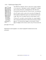
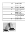
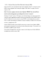
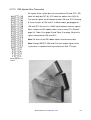
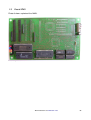
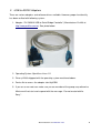
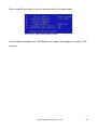
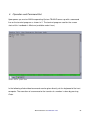
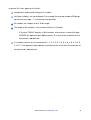
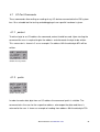
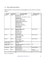
PRODUCT BRIEF SelfAssembly Kit System TRAINZ User Manual Please read carefully before power up ! Doc. Version 201310281 Author: Mario Blunk Firmware Version: MAIN V9.3 / V9.4 , V9.5 / V9.6 Hardware Version: MAIN: V0.93r4 MMU: V1.01r4 Blunk electronic at www.trainz.de Contents 1 Preface...............................................................................................................................5 2 System Overview...............................................................................................................8 3 Hardware............................................................................................................................8 3.1 Dimensions..................................................................................................................8 3.2 Board MAIN................................................................................................................9 3.2.1.Schematics and Assembly Drawings..................................................................10 3.2.2.Oscillator and System Clock...............................................................................11 3.2.3.Processor (CPU).................................................................................................11 3.2.4.Serial Interface (SIO)..........................................................................................12 3.2.5.Counter Timer Channels (CTC)..........................................................................15 3.2.6.Parallel InputOutput (PIO).................................................................................16 3.2.6.1 Configuration Handshake Signals..............................................................20 3.2.7.I²CBus 0.............................................................................................................21 3.2.8.I²CBus 1.............................................................................................................21 3.2.8.1 I²CFLASHEEPROM.................................................................................21 3.2.8.2 I²CExpander..............................................................................................22 3.2.9.External Reset and Non Maskable Interrupt (NMI)...........................................23 3.2.10.Z80System Bus Connectors............................................................................24 3.2.11.Interrupt Priority Configuration..........................................................................27 3.2.12.I/OAddresses...................................................................................................28 3.3 Board MMU...............................................................................................................29 3.3.1.Schematics and Assembly Drawings..................................................................31 3.3.2.4 kByteROM......................................................................................................32 3.3.3.27 kByteSRAM..................................................................................................32 3.3.4.32 kByteUserFLASHEEPROM.......................................................................33 3.3.5.32 kByteSRAM..................................................................................................34 3.3.6.Z80 System Bus Connectors..............................................................................35 3.3.7.Memory Map.......................................................................................................38 3.4 Power Supply............................................................................................................38 4 RS232 and Terminal Program of the Host Computer......................................................40 5 USBtoRS232Adapters..................................................................................................41 6 Operation and Command Set..........................................................................................43 6.1 I/OPort Commands..................................................................................................45 6.1.1.portout..................................................................................................................45 6.1.2.portin...................................................................................................................45 6.2 I²CCommands.........................................................................................................46 6.2.1.rsti0......................................................................................................................46 6.2.2.rsti1.....................................................................................................................46 6.2.3.i0f and i1f............................................................................................................46 6.2.4.i0p and i1p..........................................................................................................47 6.3 Administrating the Memory.......................................................................................48 6.3.1.viewmem.............................................................................................................48 6.3.2.copy....................................................................................................................49 6.3.3.comp...................................................................................................................50 6.3.4.fill........................................................................................................................50 6.3.5.prgflash...............................................................................................................50 6.3.6.eraseflash...........................................................................................................51 6.3.7.testmem..............................................................................................................52 6.3.8.load.....................................................................................................................53 6.3.9.Starting the User Program..................................................................................56 6.3.9.1 call..............................................................................................................56 6.3.9.2 Per Jumper.................................................................................................56 6.4 Miscellaneous...........................................................................................................57 6.4.1.echooff.................................................................................................................57 6.4.2.help.....................................................................................................................57 7 System Test......................................................................................................................58 8 System Calls....................................................................................................................58 8.1 Register Dump..........................................................................................................58 9 Assemblers, Interpreters and Compilers.........................................................................59 10 Device Mounting Options...............................................................................................60 11 Parts Delivered with System TRAINZ...........................................................................61 12 Full SelfAssembly Shipment Option..............................................................................61 13 RoHS conformity............................................................................................................61 14 Useful Links....................................................................................................................62 15 Further Reading.............................................................................................................64 16 Disclaimer.......................................................................................................................64 Blunk electronic at www.trainz.de 3 This page is left blank intentionally. 4 Blunk electronic at www.trainz.de 1 Preface The ZiLOG Z80 is a 8bit CISC microprocessor made and sold by ZiLOG from July 1976. It is one of the most popular microprocessors a whole generation of electronics and programmers has grown up with. It found usage in desktop and embedded computers – a wide spectrum from game console up to military applications. The Z80 derivatives and clones make this CPU the most used processor of all times. VHDL and Verilog Cores are also available (see section 14page 62 for more). System TRAINZ does not aim to compete with the powerful and sophisticated embedded computer systems of today. What is System TRAINZ good for ? software development (assembly, C, ...) education and study (basics of computer engineering, programming, repair and maintenance) control and measurement education in assembly and troubleshooting of complex electronics By consequent usage of ICs on sockets, THT devices1 and moderate clock frequencies of less than 11 Mhz the user has a robust and easy to repair computer system. System TRAINZ can be operated in the targeted application without any modifications. Photo 1 shows the hardware of System TRAINZ. 1 ThroughHoleTechnology Blunk electronic at www.trainz.de 5 History: To face the obsolescence of Z80development tools System TRAINZ has come up. It is a very simple form of such a development system. During conception of System TRAINZ the key problem was to load a binary file (mostly this is Z80machine code) into the RAM, test it and burn it into the on board FLASHEEPROM. Photo 1: System TRAINZ , view at board MAIN 6 Blunk electronic at www.trainz.de What does System TRAINZ provide ? 1. RS232interface to host computer 2. USBSupport via USBtoRS232Adapter with PL2303 chipset 3. operating via terminal program running on host computer – thus not depending on any operation system of the host computer 4. 4kByte bootloader and on board operating system 5. hardware that can operate in the targeted application 6. testing of the user written program in the 60kByte system RAM 7. programming the user written program into the system 32 kByteFLASHEEPROM 8. execution of the user written program at system start (see section 6.3.9 page 56) 9. open system bus for user made hardware extensions 10. I²C support for peripheral devices 11. The user is free to change mountings of components, to make own configurations of both hardware and software. 12. debugging via system call Register Dump What does System TRAINZ NOT provide ? 1. Any Z80 assembler, compiler or interpreter software (see section 9 page 59) 2. single step program execution 3. breakpoints 4. video interfaces like VGA, composite, ... Blunk electronic at www.trainz.de 7 2 System Overview Drawing 1 shows System TRAINZ as a whole and its interaction with the host computer. This can be any computer that is equipped with a serial RS232 interface and a terminal Drawing 1: overview System TRAINZ program. So System TRAINZ can be operated with Linux, UNIX, MSDOS and MS TRAINZ Windows. Terminal programs of these operating systems are for example Minicom or Host Computer + MAIN Terminalprogram HyperTerminal. COMx ttySx RS 232 nullmodem JP12 JP2 JP6 MMU JP407 JP405 Z80 Data & Cntrl Bus 3 Hardware Z80 Addres & Cntrl Bus For information about the RS232 settings see section 4 page 40. The physical assembly consists of two EuroBoards (100 x 160 mm), the main board MAIN JP406 and the memory board MMU (Memory Management Unit). Following sections describe the JP404 operation modes of system components related to System TRAINZ. The user is free to change them for his own needs. power suppy +5V / +12V / 12V / GND user specific periphery 3.1 Dimensions The assembly of System TRAINZ as shown by Photo 1 on page 6 make the system having the following outline: 160 x 100 x 120 mm. By removing the stand offs the two boards became loose so that the user can mount them on his own way. 8 Blunk electronic at www.trainz.de 3.2 Board MAIN A photo of this board shows Photo 2. Photo 2: top side of MAIN Blunk electronic at www.trainz.de 9 Drawings 2 shows MAIN with its most relevant components. Drawing 2: overview board MAIN MAIN JP 2 Ch A SIO CPU 3.2.1. Schematics and Assembly Drawings JP 7 Ch B LEDs D0 & 1 Oscillator + CLK selector JP5 PIO JP 10 Port A As these drawings are updated from time to time they have been removed from this JP 3 CTC CPUBus document. Please find them at: Port B JP 1 http://www.trainz.de/trainz/hw I²CFLASH I²CPIO I/OAdr Decoder EEPROM INTPriority PWR JP 20 Cntrl & Adr JP 12 / Cntrl & Data JP6 10 JP 4 Blunk electronic at www.trainz.de X1 X2 3.2.2. Oscillator and System Clock The 10Mhzmaster clock generates oscillator QG1. By means of a frequency divider the master clock gets divided by 2, 4, 8 and 16. JP5 allows the selection of the desired system clock by plugging a jumper on it. Default setting is 2,5Mhz. SeeTable 1. Drawing 3: pins of JP5 jumper plugged on system clock 10 9 0,625 Mhz 8 7 1,25 Mhz 6 5 2,5 Mhz 4 3 5 Mhz 2 1 10 Mhz comments default not tested ! Table 1: jumper positions on JP5 The frequency of the system clock directly affects the data rate of the serial interface (see section 4 page 40) as well as all other timings withing System TRAINZ. Note: A system clock higher than 2,5 Mhz can be run safely only if all components depending on it support this clock frequency. 3.2.3. Processor (CPU) Regarding the type of CPU mountable see section 10 page 60. See datasheet for more information. Blunk electronic at www.trainz.de 11 3.2.4. Serial Interface (SIO) Basically both channels A and B of the SIO can be used. System TRAINZ uses only channel A for the RS232. Transmit and receive clock of both channels is fed by the CTC unit. Please see section 3.2.5 page 15 for information on the CTC. Channel A is connected to JP2 (physical view in Drawing 4, signals in Table 2), channel B Drawing 4: pins of JP2/7 on JP7 (physical view in Drawing 4, signals in Table 3). The state of line RI (Ring Indicator) can be monitored by PIO Port B. See section 3.2.6 page 16 for more. If System TRAINZ is to be operated in an electromagnetic harsh environment the line receivers IC8 and IC10 may be equipped with external capacitors C28, 29, 30, 31 / C23, 25, 26, 27 in order to block noise from the lines RXD, CTS, DCD and RI. See datasheet of the line receivers regarding external capacitor values. The line receiver and driver IC are 1489 and 1488 compatible in order to fully meet the voltage specifications of the RS232 interface. Regarding the mounting options see section 10 page 60. See datasheets for more information. Please read about the settings of the RS232 in section 4 page 40. Operation via USBto RS232Adapter is supported. Please read more in section 5page 41. Blunk electronic at www.trainz.de 12 pin no. signal comments 9 GND maximum load 100mA ! Do NOT use as protective ground ! 8 RI via series resistor connected to PIO B4 7 DTR 6 CTS 5 TXD 4 RTS 3 RXD 10 2 1 DCD Table 2: signals of SIO channel A connected to JP2 pin no. signal comments 9 GND maximum load 100mA ! Do NOT use as protective ground ! 8 RI via series resistor connected to PIO B5 7 DTR 6 CTS 5 TXD 4 RTS 3 RXD 10 2 1 DCD Table 3: signals of SIO channel B connected to JP7 The signal wirings on JP2 and JP7 are made according to standardized adapters from 2x5 pin pinheader to 9 pin DSub (Photo 3on page 14). Table 4 on page 14 shows the wiring of this adapter which can be found in many PCs to contact the serial interface COMx or ttySx. Line DSR is not used by System TRAINZ. Pin 2 of JP2 and JP7 is not connected. Blunk electronic at www.trainz.de 13 Photo 3: RS232 adapter (ferrit core not required) 10 pol. pinheader 9 pin DSub male comments 10 9 5 signal GND 8 9 Ring Indicator (RI) 7 4 Data Terminal Ready (DTR) 6 8 Clear to Send (CTS) 5 3 Transmit (TXD) 4 7 Request to Send (RTS) 3 2 Receivce (RXD) 2 6 Data Set Ready (DSR) 1 1 Data Carrier Detect (DCD) Table 4: wiring of RS232 adapter as shown on Photo 3 Blunk electronic at www.trainz.de 14 3.2.5. Counter Timer Channels (CTC) CTC0 feeds the transmit and receive clock into SIO channel A. CTC1 feeds the transmit and receive clock into SIO channel B. CTC2 and CTC3 are used by System TRAINZ for a very simple system test. Please see section 7 on page 58 for more. JP3 (see Drawing 5) is wired to all CTCsignals according to Table 5 on Drawing 5: pins of JP3 page 15. Regarding the mounting options see section 10 page 60. See datasheet for more information. pin no. signal comments 2, 4, 6, 8, 10, 12, 14 GND total maximum load 100mA ! 13 TRG3 for system test connect to pin 11, internally pulled up by 10k resistor 11 TO2 for system test connect to pin 13 9 TRG2 internally pulled up by 10k resistor 7 TO1 5 TRG1 3 TO0 1 TRG0 internally pulled up by 10k resistor internally pulled up by 10k resistor Table 5: CTCsignals connected to JP3 Blunk electronic at www.trainz.de 15 3.2.6. Parallel InputOutput (PIO) The Z80 PIO has two ports. Port A is free for any usage. Exception is the system test – described in section 7 on page 58 ! The logical state of signals A0 and A1 is displayed by the LEDs D0 and D1. Primarily port B controls both the I²Cbuses 0 and 1, the monitoring of the RIsignals and the system start (see section 6.3.9 page 56). Minor hardware modifications by the user make port B free for any usage. Table 6 and 7 on page 18 give the wiring of port A and B. JP10 and JP1 are wired in a way that allows the usage of adapters from 2x13 pin pinhead to 25 pin DSub female connectors (Photo 4 Drawing 6: pins of JP10/1 page 18). The wiring of these adapters can be found in Table 8 page 19. Adapters of this kind are used in many PCs to connect the printer port LPTx or lpx. Regarding the mounting options see section 10 page 60. See datasheet for more information. Blunk electronic at www.trainz.de 16 pin no. signal comments 1 STRB see section 3.2.6.1 page 20 A0 state showed by D0, internally pulled up by 10k resistor A1 state showed by D1, internally pulled up by 10k resistor A2 internally pulled up by 10k resistor 9 A3 internally pulled up by 10k resistor 11 A4 internally pulled up by 10k resistor 13 A5 internally pulled up by 10k resistor 15 A6 internally pulled up by 10k resistor 17 A7 internally pulled up by 10k resistor 19 /ACK see section 3.2.6.1 page 20 21 BSY see section 3.2.6.1 page 20 10, 12, 14, 16, 18, 20, 22, 24 GND total maximum load 100mA ! 2 3 4 5 6 7 8 Table 6: signals of PIO port A connected to JP10 Blunk electronic at www.trainz.de 17 pin no. signal comments 1 STRB see section 3.2.6.1 page 20 SCL0 see section 3.2.7 page 21, internally pulled up by 10k resistor SDA0 see section 3.2.7 page 21, internally pulled up by 10k resistor B2 see section 3.2.8 page 21, internally pulled up by 10k resistor 9 B3 see section 3.2.8 page 21, internally pulled up by 10k resistor 11 B4 connected to signal RI of SIO Ch. A, internally pulled up by 10k resistor 13 B5 connected to signal RI of SIO Ch. B, internally pulled up by 10k resistor 15 B6 internally pulled up by 10k resistor 17 B7 see section 6.3.9 page 56, internally pulled up by 10k resistor 19 /ACK see section 3.2.6.1 page 21 21 BSY see section 3.2.6.1 page 20 10, 12, 14, 16, 18, 20, 22, 24 GND total maximum load 100mA ! 2 3 4 5 6 7 8 Table 7: signals of PIO port B connected to JP1 Photo 4: parallel port adapter Blunk electronic at www.trainz.de 18 26 pin pinhead 25 pin DSub female comments 1 1 /STRB 3 2 Data 0 5 3 Data 1 7 4 Data 2 9 5 Data 3 11 6 Data 4 13 7 Data 5 15 8 Data 6 17 9 Data 7 19 10 /ACK 21 11 BUSY 23 12 PAPER out 25 13 SEL out 2 14 /AUTOFD 4 15 /ERROR 6 16 /INIT 8 17 SEL in 18 25 signal GND 26 10, 12, 14, 16, 18, 20, 22, 24 Table 8: wiring of parallel port adapter as shown on Photo 4 Blunk electronic at www.trainz.de 19 3.2.6.1 Configuration Handshake Signals The handshake signals of PIO port A and B can be customized on JP11 and JP9 regarding the desired data flow. Per default no Jumper is plugged on both JP11 or JP9. Drawing 7 shows the pin numbering of JP11 and 9. Table 9 and 10 on page 20 give possible configurations. Drawing 7: Pins of JP11/9 The PIO pins /ASTRB and /BSTRB are connected internally to 10k pullup resistors. jumper plugged on signal flow 1 – 2 ARDY drives /ACK to periphery 3 – 4 ARDY drives BUSY to periphery 5 – 6 ARDY drives /STRB to periphery 7 – 8 periphery drives /STRB to ASTRB 9 – 10 periphery drives BUSY to ASTRB 11 – 12 periphery drives /ACK to ASTRB comments Table 9: jumper positions on JP11 jumper plugged on signal flow 1 – 2 BRDY drives /ACK to periphery 3 – 4 BRDY drives BUSY to periphery 5 – 6 BRDY drives /STRB to periphery 7 – 8 periphery drives /STRB to BSTRB 9 – 10 periphery drives BUSY to BSTRB 11 – 12 periphery drives /ACK to BSTRB comments Table 10: jumper positions on JP9 Blunk electronic at www.trainz.de 20 3.2.7. I²CBus 0 The Z80 PIO port B operates as master of I²Cbus 0. User specific external I²C hardware can be connected to it. I²Cbus 0 is accessible at JP1 pins 3 (SCL0) and 5 (SDA0) (see Table 7 page 18). The PIO drives from its port B0 via a series resistor the signal SCL0. Port B1 drives in the same manner signal SDA0. There is no pullup resistor for any external hardware required on SCL0 or SDA0. 3.2.8. I²CBus 1 The Z80 PIO port B operates as master of I²Cbus 1. Its purpose is to control the I²C FLASHEEPROM and I²Cexpander of board MAIN. The PIO drives from its port B2 via a series resistor the signal SCL1. Port B3 drives the same way signal SDA1. SCL1 and SDA1 are not directly wired to JP1 (see Table 7 page 18). A pullup resistor is already connected to both SCL1 and SDA1 each. 3.2.8.1 I²CFLASHEEPROM Connected to I²Cbus 1 is a FLASHEEPROM where the user may store any data. This storage is hard wired to address 001b. Depending on the type mounted this address is important when accessing the device. Regarding the mounting options see section 10 page 60. See datasheet for more information. For commands to read or write the device see section 6.2 page 46. Blunk electronic at www.trainz.de 21 3.2.8.2 I²CExpander Another member of I²Cbus 1 is the I²Cexpander, which can be used to monitor or control external periphery. The address of the I²Cexpander is hardwired to 000b. All its parallel inputs and outputs are protected against current overloading by series resistors of 160 Ohms. On the other end these resistors are connected to JP4. 160 Ohms allow direct connecting of LEDs or 7 segmentdisplays to JP4. Table 11 on page 22 shows the signals of the I²Cexpander on JP4. Please see datasheet for more information. Regarding the mountable type see section 10 page 60. Drawing 8: pins of JP4 Commands required to write or read the I²Cexpander are to be found in section 6.2 on page 46. pin no. signal 1 P7 3 P6 5 P5 7 P4 9 P3 11 P2 13 P1 15 P0 comments 17 19 /EXT_NMI see section 3.2.9 page 23 21 /EXT_RESET 23 RESET LED cathode 25, 27, 29, 31, 33 +5V total maximum load 100mA ! 2, 4, 6, 8, 10, 12, 14, 16, 18, 20, 22, 24, 26, 28, 30, 32, 34 GND total maximum load 200mA ! Table 11: signals of the I²Cexpander connected to JP4 Blunk electronic at www.trainz.de 22 3.2.9. External Reset and Non Maskable Interrupt (NMI) At pin 19 of JP4 a non maskable interrupt may be triggered. At pin 21 an external system RESET can be triggered. See Drawing 8 on page 22 and Table 11 on page 22 for the signals on JP4. Note: To ensure a proper and safe start of System TRAINZ the external Reset must be active during power up and beyond for at least 1 second ! Behind pin 19 and 21 each an RClowpass and a SchmittTrigger are implemented which shape the signals applied there and drive them to the /NMIinput and the /RESETinput of the CPU. Optionally the active external system RESET can be displayed by an external LED. It is to be connected by its cathode on JP4 pin 23 and by its anode on +5V. No series resistor is needed for the LED. System TRAINZ handles external NMI the same way as external reset: Address 0000h gets jumped to whereupon the execution of code residing there begins. The contents of all the SRAMs are NOT erased or altered. See section 6.3.9 page 56 for execution of code in the 32 kByteUserFLASHEEPROM immediate after external reset or NMI. Blunk electronic at www.trainz.de 23 3.2.10. Z80System Bus Connectors All signals of the system bus are connected to JP6 and JP12. JP6 holds the data bus D[7..0], JP12 holds the address bus A[15..0]. The control signals are distributed on both JP6 and JP12. Drawing 9 shows the pins of JP6 and 12. If ribbon cables get plugged on JP6 and JP12 the result is a GND signal between two bus signals. Most suitable are IDEribbon cables used in many PCs (Photo 5 page 24). Table 12 on page 25 and Table 13 on page 26 give the signals connected to JP6 and JP12. Note: All wires of the IDEribbon cables must be accessible. Note: Except /RESET, /NMI and CLK each output signals of the system bus is capable of driving maximal one Std. TTL input. Drawing 9: pins of JP6/12 Photo 5: 40 pin IDE connector Blunk electronic at www.trainz.de 24 pin no. signal comments 2 D0 not buffered 4 D1 not buffered 6 D2 not buffered 8 D3 not buffered 10 D4 not buffered 12 D5 not buffered 14 D6 not buffered 16 D7 not buffered 18 reserved 20 /M1 not buffered 22 /MREQ not buffered 24 /IOREQ not buffered 26 /RD not buffered 28 /WR not buffered 30 /RFSH not buffered 32 /HALT 34 /WAIT has an internal 10k pullupresistor 36 /BUSREQ has an internal 10k pullupresistor 38 /BUSACK not buffered 40 system clock CLK 1, 3, 5, 7, 9, 11, 13, GND 15, 17, 19, 21, 23, 25, 27, 29, 31, 33, 35, 37, 39 total maximum load 100mA ! Table 12: system bus signals connected to JP6 Blunk electronic at www.trainz.de 25 pin no. signal comments 2 A0 not buffered 4 A1 not buffered 6 A2 not buffered 8 A3 not buffered 10 A4 not buffered 12 A5 not buffered 14 A6 not buffered 16 A7 not buffered 18 A8 not buffered 20 A9 not buffered 22 A10 not buffered 24 A11 not buffered 26 A12 not buffered 28 A13 not buffered 30 A14 not buffered 32 A15 not buffered 34 EXT IEI see section 3.2.11 page 27 36 /INT not buffered, has an internal 10k pullup resistor 38 /NMI has an internal 10k pullupresistor, see section 3.2.9 page 23 40 /RESET has an internal appr. 80 Ohms pullup resistor, see section 3.2.9 page 23 1, 3, 5, 7, 9, 11, 13, GND 15, 17, 19, 21, 23, 25, 27, 29, 31, 33, 35, 37, 39 total maximum load 100mA ! Table 13: system bus signals connected to JP12 Blunk electronic at www.trainz.de 26 3.2.11. Interrupt Priority Configuration To JP20 the IEO/IEO signals of CTC, SIO, PIO and the IEI signal of the external periphery are connected. Here the configuration of the interrupt priority order is possible. Drawing 10 shows the pin numbers of JP20 and Table 14 gives the signals connected to it. Please do not change jumper positions of pins 11 to 17. Per default 15 and 16 are connected. Drawing 10: pins of JP20 pin no. signal comments 10 +5V maximum load 100mA ! 9 CTC IEI via Jumper per default connected to pin 10, internally connected to a 10 pullup resistor 8 SIO IEI via Jumper per default connected to pin 7, internally connected to a 10 pullup resistor 7 CTC IEO via Jumper per default connected to pin 8 6 SIO IEO via Jumper per default connected to pin 5 5 PIO IEI via Jumper per default connected to pin 6, internally connected to a 10 pullup resistor 4 external IEI via Jumper per default connected to pin 3 3 PIO IEO via Jumper per default connected to pin 4 2 GND total maximum load 50mA ! 1 GND total maximum load 50mA ! Table 14: interrupt configuration signals connected to JP20 Thus per default following priority order is set: 1. CTC (highest priority) 2. SIO 3. PIO 4. external periphery (lowest priority) Blunk electronic at www.trainz.de 27 3.2.12. I/OAddresses Table 15 gives an overview of I/Oaddresses already used by System TRAINZ. periphery / channel I/Oaddress CTC / 0 00h CTC / 1 01h CTC / 2 02h CTC / 3 03h SIO A / Data 04h SIO A / Control 06h SIO B / Data 05h SIO B / Control 07h PIO A / Data 08h PIO A / Control 0Ah PIO B / Data 09h PIO B / Control 0Bh comments Table 15: I/Oaddresses of System TRAINZ Blunk electronic at www.trainz.de 28 3.3 Board MMU Photo 6 shows a photo of the MMU. Photo 6: top side of MMU Blunk electronic at www.trainz.de 29 Drawing 11 illustrates the board MMU with its most relevant components. Drawing 11: overview of board MMU MMU 32 kByte User FLASHEEPROM 27 kByte SRAM 32 kByte SRAM Mem Adr Decoder CPUBus 4 kByte ROM FLASH configuration JP 200 PWR Cntrl & Adr JP 405, JP407 / Cntrl & Data JP 404, JP406 X400 Blunk electronic at www.trainz.de 30 3.3.1. Schematics and Assembly Drawings As these drawings are updated from time to time, they have been removed from this document. Please find them at: http://www.trainz.de/trainz/hw Blunk electronic at www.trainz.de 31 3.3.2. 4 kByteROM The read only memory block holds the tiny operating system and the bootloader of System TRAINZ and uses the address range shown in Table 18 on page 38. Regarding the mountable type see section 10 on page 60. Please read the datasheet for more. 3.3.3. 27 kByteSRAM The mounting of this memory block is mandatory for the operating system of System TRAINZ. This memory block is free for use by the user. Files to be downloaded from the host computer into System TRAINZ may be put onto any location within these 27 kBytes of RAM. Please see section 6.3.8 on page 53 for more. The content of this memory block is NOT erased or altered by NMI or system Reset. Regarding the mountable type see section 10 on page 60. Please read the datasheet for more. Blunk electronic at www.trainz.de 32 3.3.4. 32 kByteUserFLASHEEPROM The user is free to store his own non volatile data or program code here. To program this memory area specific commands are available. Please read section 6.3 on page 48 for more. Table 18 on page 38 gives an overview of the address rage used by the 32 kByte userFLASHEEPROM. It's possible to execute code residing there immediately after system reset or by a specific command. More can be read in section 6.3.9 on page 56. The 32 kByteuserFLASHEEPROM can be mounted only, when the 32kByteSRAM is NOT mounted. Due to the same address range these two blocks share, both can not be mounted at the same time. See Table 18 on page 38. JP200 (see Drawing 12) allows the setup of a hardware write protection for the 32 kByteuserFLASH EEPROM: pin 18 connected to pin 20 – protection active pin 18 connected to pin 17 – writing allowed (default setting)2 Drawing 12: pins of JP200 Per default some more jumpers are plugged on JP200. Please do not change them: pin 5 connected to pin 6 pin 7 connected to pin 8 pin 9 connected to pin 10 pin 11 connected to pin 12 pin 14 connected to pin 16 Regarding the mountable type see section 10 on page 60. Please read the datasheet for more. 2 In order to have write access to a RAM mounted here instead of the FLASHEEPROM this setting is a must. Blunk electronic at www.trainz.de 33 NOTE: The operating system of System TRAINZ version 9.4 and onwards supports programming of the FLASH type AM29F040. Type W29C020 (WINBOND) has been discontinued by WINBOND and is not supported any more since version 9.4. 3.3.5. 32 kByteSRAM As an alternative to the 32 kByteuserFLASHEEPROM the upper 32 kByteSRAM can be mounted. In addition to the lower 27 kByteSRAM a total range of 59 kByte SRAM becomes available for the user. Files downloaded from the host computer into system TRAINZ may reside on any location within this 59 kByte. Please read section 6.3.8 on page 53 for more. The content of this memory block is NOT erased or altered by NMI or system Reset. Note: On JP200 pin 18 must be connected to pin 17 in order to have write permission to the 32 kByteSRAM ! See Drawing 12 on page 33. The 32 kByteSRAM can be mounted only if the 32kByteUserFLASHEEPROM is NOT mounted since these two memory blocks share the same address range. See Table 18 on page 38. Regarding the mountable type see section 10 on page 60. Please read the datasheet for more. Blunk electronic at www.trainz.de 34 3.3.6. Z80 System Bus Connectors All signals of the system bus are connected to JP405/407 and JP404/406 (see Drawing 13 on the left). JP405 and JP407 are connected in parallel, JP404 and JP406 are connected in parallel. This way the user can attach his own hardware easily to System TRAINZ. If ribbon cables are plugged on JP405/407 and JP404/406 an alternating order of GND, bus signal, GND and so on results. Common IDEribbon cables as they are used in PCs are suitable. Table 16 and Table 17 on pages 36 and 37 show the signals of JP404 through JP407. Note: All wires of the IDEribbon cables must be accessible. Note: Please read the comments Table 12 on page 25 and Table 13 on page 26 if you attach your own hardware extensions. Drawing 13: pins of JP404 407 Photo 7: System Bus Connectors on MMU Blunk electronic at www.trainz.de 35 pin no. signal comments 2 D0 has an internal 10k pullupresistor 4 D1 has an internal 10k pullupresistor 6 D2 has an internal 10k pullupresistor 8 D3 has an internal 10k pullupresistor 10 D4 has an internal 10k pullupresistor 12 D5 has an internal 10k pullupresistor 14 D6 has an internal 10k pullupresistor 16 D7 has an internal 10k pullupresistor 18 RSVD0 reserved 20 /M1 22 /MREQ 24 /IOREQ 26 /RD has an internal 10k pullupresistor 28 /WR has an internal 10k pullupresistor 30 /RFSH 32 /HALT 34 /WAIT 36 /BUSREQ 38 /BUSACK 40 System clock CLK 1, 3, 5, 7, 9, 11, 13, GND 15, 17, 19, 21, 23, 25, 27, 29, 31, 33, 35, 37, 39 has an internal 10k pullupresistor has an internal 10k pullupresistor total maximum load 100mA ! Table 16: system bus signals connected to JP404 and JP406 Blunk electronic at www.trainz.de 36 pin no. signal comments 2 A0 has an internal 10k pullupresistor 4 A1 has an internal 10k pullupresistor 6 A2 has an internal 10k pullupresistor 8 A3 has an internal 10k pullupresistor 10 A4 has an internal 10k pullupresistor 12 A5 has an internal 10k pullupresistor 14 A6 has an internal 10k pullupresistor 16 A7 has an internal 10k pullupresistor 18 A8 has an internal 10k pullupresistor 20 A9 has an internal 10k pullupresistor 22 A10 has an internal 10k pullupresistor 24 A11 has an internal 10k pullupresistor 26 A12 has an internal 10k pullupresistor 28 A13 has an internal 10k pullupresistor 30 A14 has an internal 10k pullupresistor 32 A15 has an internal 10k pullupresistor 34 EXT IEI 36 /INT 38 /NMI 40 /RESET 1, 3, 5, 7, 9, 11, 13, GND 15, 17, 19, 21, 23, 25, 27, 29, 31, 33, 35, 37, 39 has an internal 10k pullupresistor total maximum load 100mA ! Table 17: system bus signals connected to JP405 and JP407 Blunk electronic at www.trainz.de 37 3.3.7. Memory Map Table 18 shows the memory map of System TRAINZ. memory block usage comments FFFFh 32 kByte 8000h SRAM or FLASHEEPROM write protection per jumper for user program possible resides in IC201 7FFFh 27 kByte 1800h SRAM for user program 17FFh 2 kByte 1000h SRAM for operating system physically in the same IC as the 27 kByte SRAM block of System TRAINZ for the user program resides in IC202 0FFFh 4 kByte 0000h ROM for operating system of System TRAINZ physically in the same IC as the 2 kByte SRAM block of the operating system of System TRAINZ resides in IC203 resides in IC200 Table 18: memory map of System TRAINZ 3.4 Power Supply Board MAIN: The operating voltages of +5V , +12V and 12V of the board MAIN are to be fed into X1. Use X2 as power output for +5V and GND to supply the board MMU. See top assembly drawing for the labeling of X1 and X2. The green LEDs D4, D5 and D6 display the presence of these three operating voltages. operating voltage current consumption comments +5V appr. 80 mA without MMU, no jumpers, no adapters +12V appr. 50 mA without MMU, no jumpers, no adapters 12V appr. 50 mA without MMU, no jumpers, no adapters Table 19: power consumption of board MAIN Blunk electronic at www.trainz.de 38 Board MMU: The operating voltage +5V of the board MMU is to be fed into X400. Please see top assembly drawing for labeling of X200. The green LED D400 displays the presence of the operating voltage. operating voltage +5V current consumption appr. 40 mA comments without MAIN, jumpers in default position Table 20: power consumption MMU operating voltage current consumption comments +5V app. 150 mA at 2,5Mhz system clock, all jumpers in default position +12V app. 50 mA serial connection to host computer established 12V app. 50 mA serial connection to host computer established Table 21: total power consumption System TRAINZ Warning: Both the boards MAIN and MMU do NOT provide any protection against overvoltage or wrong connecting of the power lines ! The tolerance of the +5V operating voltage must not exceed +/0,25V ! The tolerance of the operating voltages +12V and 12V must be withing range of the operating voltage specified in the datasheets of the fitted RS232 line drivers and receivers ! Beyond this limits malfunctions or damage of System TRAINZ may occur. Blunk electronic at www.trainz.de 39 4 RS232 and Terminal Program of the Host Computer On the host computer a terminal program is required. Users running Linux or Solaris may use Minicom, under MSWindows the Hyper Terminal program is recommended. On Linux, if you are a nonroot user make sure you are member of the group uucp otherwise Minicom will not start and respond with the message: “Cannot create lockfile. Sorry.”. Please make sure there is a serial interface in your computer at all. COM or ttyS ports are increasingly less to be found in laptop PCs. Thus connecting the Unit via a USBtoRS232 Adapter is needed. Please see section5on page 41 for more on this. The parameters of the RS232 interface to communicate with System TRAINZ are to be set somewhere within the terminal program: data transfer rate 9600 bit/s 8 bits per character no parity 1 stop bit hardware flow control3 The data transfer rate can be increased to 19200 bit/s by doubling the frequency of the system clock. Please read section 3.2.2 on page 11 for more. Per default every character received by System TRAINZ gets echoed back to the host computer which makes the character visible on the screen 4. This way allows the verification of the character sent by the host computer. In order to reduce the data traffic the echo can be disabled. Please read section 6.4.1 on page 57 for more. The communication of System TRAINZ with the host computer is designed to allow automated communication like scripting with Kermit. 3 Since operating system version 9.4 the auto enables feature of the Z80 SIO is used in order not to override an eventually slow host computer. 4 provided the respective character is a “visible one” at all Blunk electronic at www.trainz.de 40 5 USBtoRS232Adapters There are various adapters and software drivers available. However, proper functionality has been verified with following system: 1. Adapter: “PL2303HX USB to Serial Bridge Controller” (Manufacturer Proflific at http://www.prolific.com.tw). See photo below. 2. Operating System OpenSuse Linux 11.1 3. Driver pl2303 shippped with the operating system mentioned above. 4. Device file to access the adapter: /dev/ttyUSB0 5. If you are a nonroot user make sure you are member of the group uucp otherwise Minicom will not start and respond with the message: “Cannot create lockfile. Sorry.”. Blunk electronic at www.trainz.de 41 When using Minicom under Linux the interface settings are shown below. Screen shot 1: USB2Serial interface settings In the hardware management of MSWindows the adapter should appear as regular COM interface. Blunk electronic at www.trainz.de 42 6 Operation and Command Set Upon power up, reset or NMI the operating System TRAINZ comes up with a command line on the terminal program as shown in 2. The terminal program used for the screen shots of this handbook is Minicom (available under Linux). Screen shot 2: system start In the following all described commands can be given directly via the keyboard of the host computer. The execution of a command or the transfer of a number is done by pressing Enter. Blunk electronic at www.trainz.de 43 In general this rules apply for all entries: hexadecimal reading and writing of all numbers Half bytes (nibbles) are not accepted. For example the entered number 4D0 brings up the error message „..?“ and cancels the operation. All numbers are integers of 8 or 16 bit length. The length of the number is not checked further on. Example: If System TRAINZ expects a 16 bit number and receives instead a 45 oder 45EADD the operation gets not canceled. The result of the execution of the command is not defined. If a number contains any character but 0, 1, 2, 3, 4, 5, 6, 7, 8, 9, a, b, c, d, e, f, A, B, C, D, E, F, the operation does not get canceled and the result after the execution of the command is not defined. Blunk electronic at www.trainz.de 44 6.1 I/OPort Commands These commands allow writing or reading of any I/O devices connected to the Z80 system bus. So a valuable tool for testing and debugging of user specific hardware is given. 6.1.1. portout To write a byte to an I/Oaddress the command portout should be used. Upon starting the command the user is required to give the address and afterwards the byte to be written. This succession is shown in 3 as an example: On address 0Ah the data byte 0Fh will be written. Screen shot 3: portout 6.1.2. portin Screen shot 4: portin In order to read a data byte from an I/Oaddress the command portin is suitable. The command asks the user for the respective address, whereupon the data read there is returned to the user. 4 shows an example of reading from address 08h the data byte FCh. Blunk electronic at www.trainz.de 45 6.2 I²CCommands Using these commands the user can write or read from the I²Cbuses 0 and 1 (see section 3.2.7 on page 21 and section 3.2.8 on page 21 for information about the hardware). 6.2.1. rsti0 This command brings all the members of I²Cbus 0 to a reset condition. 6.2.2. rsti1 This command brings all the members of I²Cbus 1 to a reset condition. 6.2.3. i0f and i1f With i0f or i1f an I²CFLASHEEPROM connected to I²Cbus 0 or 1 can be read or written. These devices must be addressed by a 8 bit device address and a 8 bit memory address 5. The LSB of the device address determines read or write access: 0 – write access, 1 – read access. 5 shows an example for reading using command i1f : From device A1h, memory address 00h, the data byte 10h is read. Screen shot 5: i1f 5 The AT24C08 made by Atmel is one of this kind. Blunk electronic at www.trainz.de 46 In 6 a write access using command i1f is shown: Into device A0h, memory address 00h, the data byte 78h is written. Screen shot 6: i1f 6.2.4. i0p and i1p By means of the commands i0p or i1p an I²Cexpander connected to I²CBus 0 or 1 can be written or read, provided it has a 8 bit device address6. The LSB of the device address determines read or write access: 0 – write access, 1 – read access. 7 shows an example how to read with command i1f : From device 41h the data byte 10h is read. Screen shot 7: i1p 8 whereas pictures how to write using command i1f : Into device 40h the data byte 55h is written. Screen shot 8: i1p 6 For example the PCF8574x by Philips is suitable. Blunk electronic at www.trainz.de 47 6.3 Administrating the Memory This section describes commands that affect only the memory area addressable directly by the Z80CPU which ranges from 0000h to FFFFh. Warning: These commands to not incorporate any protection against overwriting of system relevant memory areas ! Please see Table 18 on page 38. 6.3.1. viewmem To get a view of 100h or 256d consecutive bytes within the system memory the command viewmem should be used. An example of how to use it have a look at 9: The contents of the memory area from 1800h to 18FFh is displayed here. After starting the command viewmem the user is requested to give the first address to be displayed (This can be even an odd number like 1701h.). The output is a view of the contents of the memory. In this example all locations are filled by 00h. Blunk electronic at www.trainz.de 48 Screen shot 9: viewmem 6.3.2. copy Frequently the content of a memory area has to be copied into another area. This can be done using the command copy. 10 shows an example of how to use it: The 30h bytes residing from address 1800h upward are copied to address 7000h upward. Screen shot 10: copy Blunk electronic at www.trainz.de 49 6.3.3. comp In case two memory areas need to be compared with each other the command comp is suitable as shown in 11: 30h bytes residing from memory address 1800h upward get compared with 30h bytes residing from address 7000h upward. If these areas match each other comp returns to the prompt without any claim. Screen shot 11: comp Screen shot 12: comp If there is a mismatch the command returns the respective address of the destination area and the expected and read data byte. 12 shows the case of a mismatch at address 7030h where a 1Ah is expected but a 00h is found instead. 6.3.4. fill Using fill a RAM memory area can be filled by a certain data byte. This command is also well applicable to modify a single data byte within the RAM. In the example shown in 13 30h bytes from address 7000h upward are filled by AAh. Screen shot 13: fill 6.3.5. prgflash Given the 32k ByteUserFLASHEEPROM is mounted, it can be programmed by prgflash. The write protection must be deactivated. Please see section 3.3.4 on page 33 for more information. 14 shows in an example how to program 100h bytes residing from address Blunk electronic at www.trainz.de 50 7000h (RAM area) upward into the address 8000h and upward of the 32k byteuser FLASHEEPROM. In the beginning of the program process the device ID code of the 32k byteuserFLASHEEPROM is displayed (in case of the AM29F040 it reads 01A4h). This code gets read only, not verified ! Afterward the 32k byteuserFLASHEEPROM gets first erased and then programmed byte wise using the DQ7 polling algorithm according to its datasheet. Screen shot 14: prgflash There is no need to erase the 32k byteuserFLASHEEPROM prior to programming. Warning: prgflash does not verify the data programmed. To verify the data that has been programmed please use the command comp after programming ! 6.3.6. eraseflash In order to erase the 32k byteuserFLASHEEPROM completely use command eraseflash. This command works like eraseflash but does not program any data into the device. Warning: eraseflash does not verify the memory content against FFh after erasing. Please use the command comp in order to verify the device has been erased completely. Blunk electronic at www.trainz.de 51 6.3.7. testmem For a very simple detection of the highest available RAM address the command testmem is recommended. It does not perform a real memory test. If the 27 kbyteSRAM is mounted only the command testmem returns the value 7FFFh (see example on 15). The value FFFFh gets returned if the optional 32 kbyteSRAM is mounted. Screen shot 15: testmem Warning: The command testmem clears the whole user RAM area to a value of 00h on all locations ! Blunk electronic at www.trainz.de 52 6.3.8. load If the user wants to download a file from the host computer into System TRAINZ the command load is provided. 16 shows the usage of load in an example: After entering and starting the command the user is asked for the address where the file should be loaded at. The destination address must be within the RAM area of System TRAINZ. From now the user has 16 seconds7 to transfer the file per Xmodem protocol with his terminal program. (see 17, 18 and 19). If these 16 seconds expire before the user starts the transfer the system will hang and has to be restarted. Screen shot 16: load Screen shot 17: xmodem 7 16 sec are vaild at a system clock of 2,5Mhz. See section 3.2.2 on page 11 for more. Blunk electronic at www.trainz.de 53 Screen shot 18: file menu Blunk electronic at www.trainz.de 54 Screen shot 19: transfer After successful file transfer load returns to the prompt. Garbled data blocks are resent maximal 9 times whereupon the transfer gets canceled. If the host computer cancels the transfer for other reasons while a block is being sent the host is required to send the missing number of bytes. This is easily accomplished by holding any key pressed until the prompt comes back. Blunk electronic at www.trainz.de 55 6.3.9. Starting the User Program The user program residing in the RAM or the 32 kbyteFLASHEEPROM can be started by two ways: 1. per software command call 2. per jumper connecting pin 17 and 18 of JP1 (see Table 7 on page 18) 6.3.9.1 call If executable Z80machine resides somewhere within the memory it can be called by the command call. In general this is a call to a subroutine. The program called should have a RET instruction at its end to allow a return to the operating system TRAINZ 8. Upon return of the user program call returns to the prompt. 20 shows an example on how to call the code residing at address 8000h. Screen shot 20: call 6.3.9.2 Per Jumper If you connect pins 17 and 18 of JP1 by plugging a jumper on them (see Table 7 on page 18) address 8000h will be jumped to after power up or reset. In contrast to command call this is no subroutine call but an unconditional jump to the fixed address 8000h. The purpose of this way of start up is to run the user program residing in the 32 kByte FLASHEEPROM shortly after power up or reset9. 8 This is just a recommendation. A return is not mandatory. 9 There are still a few machine instructions System TRAINZ executes following reset or power up in order to read the status of pins 17 and 18 of JP1. Blunk electronic at www.trainz.de 56 6.4 Miscellaneous 6.4.1. echooff The command echooff turns of the echo function of the serial interface to the host computer (see section 4 on page 40). This is useful to reduce the data traffic when operating System TRAINZ automated by a program running at the host computer (e.g. Kermit). By starting echooff the user does not see his entries any more on the terminal screen. Only by cold start or reset the echo can be enabled again. 6.4.2. help The full command set of System TRAINZ can be listed by the command help. 21 shows the output of this command. Screen shot 21: help Blunk electronic at www.trainz.de 57 7 System Test If the pins 11 and 13 of JP3 are connected, the LEDs D0 and D1 flash in the order of a 2 bit binary counter. This gives a very crude statement of the functionality of CPU, CTC, PIO, 4 kByteROM, oscillator and wiring between the boards MAIN and MMU. Note: As long as the system test is running no entries are allowed from the host computer. 8 System Calls On request the user will be given memory addresses of the operating system and bootloader of System TRAINZ. This way the user gets access to various routines that allow for example I²C operation or xmodem file transfer. 8.1 Register Dump Currently the most important routine is Register Dump, which when called from the user program, outputs the contents of the current CPU foreground registers, the index registers IX and IY, the program counter PC, the stack pointer SP and the interrupt register IR. Whenever the mainline program calls this routine by the command CALL 0BB6h the register contents are sent to the host computer to be displayed there. Of course this routine can also be called from the prompt of the operating system as shown below: This routine does not alter the content of any register. It merely outputs their contents prior to calling Register Dump and restores them when returning to the mainline program. So the user has a tool to debug her/his program at runtime. Blunk electronic at www.trainz.de 58 9 Assemblers, Interpreters and Compilers This section just gives the link to the official Z80 homepage. Various compilers, simulators or assemblers can be downloaded there for free: http://www.z80.info Blunk electronic at www.trainz.de 59 10 Device Mounting Options Table 22 provides an overview of device mounting options of most relevant ICs of System TRAINZ. device package type mountable delivery state Z80CPU DIL40 BU18400APS (ROHM) D780C1(NEC) KP1858BM1/2/3 / KR1858BM1/2/3 (USSR) LH0080 (Sharp) MK3880x (Mostek) T34VM1 / T34BM1 (USSR) TMPZ84C00AP8 (Toshiba) UA880 / UB880 / VB880D (MME) Z0840004 (ZiLOG) Z0840006 (ZiLOG) Z80ACPUD1 (SGSAtes) Z84C00AB6 (SGSThomson) Z84C00 (ZiLOG) Z8400A (Goldstar) U84C00 (MME) Z84C00 (ZiLOG) Z80SIO Typ 0 DIL40 UA8560 , UB8560 (MME) Z0844004 (ZiLOG) Z8440AB1 (ST) Z0844006 (ZiLOG) Z84C40 (ZiLOG) U84C40 (MME) Z84C40 (ZiLOG) Z80PIO DIL40 Z0842004/6 (ZiLOG) UA855 / UB855 (MME) Z84C20 (ZiLOG) U84C20 (MME) Z84C20 (ZiLOG) Z80CTC DIL28 Z84C30 (ZiLOG) U84C30 (MME) UA857 / UB857 (MME) Z84C30 (ZiLOG) 27 kByteSRAM 32 kByteSRAM DIL28 UM62256 (UMC) HM62256 32 kByte FLASH DIL32 4 kByte ROM W29C020C90 Z (Winbond) discontinued AM29F040 (AMD) A29040B (AMIC) N/A I²CExpander DIL16 PCF8574 (Philips) PCF8574A (Philips) PCF8574 (Philips) I²CFLASH DIL8 AT24C08 (Atmel) ST24C08 (STMicroelectronics) ST24C08 (STMicroelectronics) Table 22: mounting options Blunk electronic at www.trainz.de 60 11 Parts Delivered with System TRAINZ System TRAINZ is assembled and delivered as kit and with these components to be fitted or plugged according to the users requirements: 1. 1x board MAIN (mountings corresponding to Table 22 page 60) 2. 1x board MMU (mountings corresponding to Table 22 page 60) 3. 2x 40 pin ribbon cable (corresponding to Photo 5 page 24) 4. 1x adapter for serial interface RS232 without ferrite core (corresponding to Table 4 page 14) 5. 1x adapter for parallel interface (corresponding to Table 8 page 19) 6. 1x 32 kByteFLASHEEPROM (corresponding to section 3.3.4 page 33) 7. 1x 32 kByteSRAM as accessory (corresponding to section 3.3.5 page 34) 12 Full SelfAssembly Shipment Option You may order just the two bare boards MMU and MAIN without any devices soldered on them. 13 RoHS conformity The kit System TRAINZ is RoHS compliant. Blunk electronic at www.trainz.de 61 14 Useful Links Find updates of this document at http://www.trainz.de Debug SPI, I²C, Boundary Scan/JTAG and other hardware with the Logic Scanner at http://www.trainz.de/logic_scanner/Logic_Scanner_UM.pdf Blunk electronic at www.trainz.de 62 Simplify Hardware Debugging with System M1 the Boundary Scan/JTAG Tester at http://www.trainz.de/bsm/BSM_Product_Brief_en.pdf The powerful communication tool Kermit at http://www.columbia.edu/kermit/ Z80 Verilog and VHDL Cores at http://www.castinc.com and http://opencores.org Z80 Application Notes at http://www.trainz.de/trainz/index.html The Z80 history at http://en.wikipedia.org/wiki/Zilog_Z80 The XModem Protocol Reference at http://www.trainz. de/trainz/pdf/xymodem.pdf The office alternative : LibreOffice at http://www.libreoffice.org EAGLE an affordable and very efficient schematics and layout tool at http://www.cadsoftusa.com/ Blunk electronic at www.trainz.de 63 15 Further Reading I recommend to read these books: “Using CKermit” / Frank da Cruz, Christine M. Gianone / ISBN 1555581080 (english) “CKermit : Einführung und Referenz” / Frank da Cruz, Christine M. Gianone / ISBN 3882290234 (german) 16 Disclaimer This manual is believed to be accurate and reliable. I do not assume responsibility for any errors which may appear in this document. I reserve the right to change devices or specifications detailed herein at any time without notice, and do not make any commitment to update the information contained herein. I do not assume responsibility for any design errors which may appear in the hardware nor in the software of System TRAINZ nor for modifications made by the user. This product is not authorized for use as critical component in life support devices or systems. Specifications mentioned in this manual are subject to change without notice. My Boss is a Jewish Carpenter Blunk electronic / Owner : Dipl.Ing. Mario Blunk / Buchfinkenweg 5 / 99097 Erfurt / Germany +49 176 2904 5855 / http://www.trainz.de © 2013 Mario Blunk Printed in Germany Blunk electronic at www.trainz.de 64