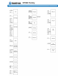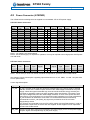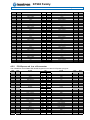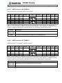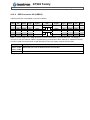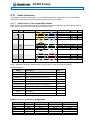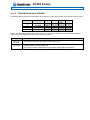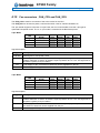
1
KT965 Family KTD-00699-S Public User Manual Date: 2010-04-15 Page 1 of 90 User Manual for the Motherboards: KT965/Flex KT965/ATXP KT965/ATXE KT965 Family KTD-00699-S Public User Manual Date: 2010-04-15 Page 2 of 90 Document revision history. Revision Date By S April 15th 2010 MLA R Oct. 19th 2009 MLA Q Oct. 13th 2009 MLA P June 9th 2009 MLA O Dec. 10th 2008 MLA N May 30th 2008 MLA M April 22nd 2008 MLA L April 2nd 2008 MLA K Mar. 6th 2008 MLA J Jan. 2nd 2008 MLA 0-I Oct. 17th, 2007 MLA Comment Updated Voltage Monitor read out. Updated warning info to installation guide. APM information corrected. Minor corrections. BIOS part features added, minor corrections and layout changed. Corrected BIOS SpeedStep info. Added “mounting the board to chassis”. Minor layout changes. TPM support added. Battery alternative added. CPU E4700 added. Correction to LAN connector pinning. Added BIOS setting: PCI Slot-2 IRQ Preference. Added note on XP for ACPI USB Wakeup. Added info to USB Function in BIOS description. PCI Riser info corrected. MTBF values added. CPU list updated. Minor layout changes. Added info on BIOS version when using XP SP3. Battery type updated. Added Windows Vista support. 3.3V tolerance increased. CPU list updated. Text “WinCE support” removed. In BIOS description: Deleted remaining Floppy controller info and corrected IO Controller version to 627DHG. Battery load information added. For BIOS part: Added APM settings, changed SpeedStep setting, added note on ETH1/2 WOL, change name of Vanderpool to Virtualization, ACPI settings modified and IDE description changed. Other minor changed. “LPT” replaced with “Printer”. BIOS function “Long Splash” added. Minor corrections to “Onboard connectors”. 4K7 added to FAN Tables. Added CPU Q6600 and Q6700. (Text removed in revision O of this document) Copyright Notice: Copyright © 2007, KONTRON Technology A/S, ALL RIGHTS RESERVED. No part of this document may be reproduced or transmitted in any form or by any means, electronically or mechanically, for any purpose, without the express written permission of KONTRON Technology A/S. Trademark Acknowledgement: Brand and product names are trademarks or registered trademarks of their respective owners. Disclaimer: KONTRON Technology A/S reserves the right to make changes, without notice, to any product, including circuits and/or software described or contained in this manual in order to improve design and/or performance. Specifications listed in this manual are subject to change without notice. KONTRON Technology assumes no responsibility or liability for the use of the described product(s), conveys no license or title under any patent, copyright, or mask work rights to these products, and makes no representations or warranties that these products are free from patent, copyright, or mask work right infringement, unless otherwise specified. Applications that are described in this manual are for illustration purposes only. KONTRON Technology A/S makes no representation or warranty that such application will be suitable for the specified use without further testing or modification. KT965 Family KTD-00699-S Public User Manual Date: 2010-04-15 Page 3 of 90 Life Support Policy KONTRON Technology’s PRODUCTS ARE NOT FOR USE AS CRITICAL COMPONENTS IN LIFE SUPPORT DEVICES OR SYSTEMS WITHOUT EXPRESS WRITTEN APPROVAL OF THE GENERAL MANAGER OF KONTRON Technology A/S. As used herein: 1. Life support devices or systems are devices or systems which, (a) are intended for surgical implant into body, or (b) support or sustain life and whose failure to perform, when properly used in accordance with instructions for use provided in the labeling, can be reasonably expected to result in significant injury to the user. 2. A critical component is any component of a life support device or system whose failure to perform can be reasonably expected to cause the failure of the life support device or system, or to affect its safety or effectiveness. KONTRON Technology Technical Support and Services If you have questions about installing or using your KONTRON Technology Product, check this User’s Manual first – you will find answers to most questions here. To obtain support, please contact your local Distributor or Field Application Engineer (FAE). Before Contacting Support: Please be prepared to provide as much information as possible: CPU Board 1. Type. 2. Part-number. 3. Serial Number. Configuration 1. CPU Type, Clock speed. 2. DRAM Type and Size. 3. BIOS Revision (Find the Version Info in the BIOS Setup). 4. BIOS Settings different than Default Settings (Refer to the BIOS Setup Section). System 1. O/S Make and Version. 2. Driver Version numbers (Graphics, Network, and Audio). 3. Attached Hardware: Harddisks, CD-rom, LCD Panels etc. KT965 Family KTD-00699-S Public User Manual Date: 2010-04-15 Page 4 of 90 Table of contents: 1. INTRODUCTION .....................................................................................................................................7 2. INSTALLATION PROCEDURE ..............................................................................................................8 2.1 Installing the board............................................................................................................................8 2.2 Requirement according to EN60950 ..............................................................................................10 3. SYSTEM SPECIFICATION ...................................................................................................................11 3.1 Component main data .....................................................................................................................11 3.2 System overview ..............................................................................................................................14 3.3 Processor support table..................................................................................................................15 3.4 System Memory support .................................................................................................................16 3.4.1 Memory Operating Frequencies .................................................................................................16 3.4.2 Memory Configurations...............................................................................................................16 3.5 KT965 Graphics Subsystem ...........................................................................................................18 3.5.1 Intel GMA 3000 Graphics Controller...........................................................................................18 3.5.2 Dynamic Video Memory Technology (DVMT) ............................................................................18 3.5.3 Advanced Digital Display (ADD2) card Support .........................................................................19 3.6 KT965 Power State Map ..................................................................................................................20 3.7 Power Consumption ........................................................................................................................22 3.8 KT965 Clock Distribution ................................................................................................................24 4. CONNECTOR DEFINITIONS................................................................................................................25 4.1 Connector layout..............................................................................................................................26 4.1.1 KT965/Flex..................................................................................................................................26 4.1.2 KT965/ATXP ...............................................................................................................................27 4.1.3 KT965/ATXE ...............................................................................................................................28 4.2 Power Connector (ATXPWR) ..........................................................................................................29 4.3 Keyboard and PS/2 mouse connectors .........................................................................................30 4.3.1 Stacked MINI-DIN keyboard and mouse Connector (MSE & KBD) ...........................................30 4.3.2 Keyboard and mouse pin-row Connector (KBDMSE) ................................................................30 4.4 Display Connectors .........................................................................................................................31 4.4.1 CRT Connector (CRT) ................................................................................................................31 4.5 PCI-Express Connectors.................................................................................................................32 4.5.1 PCI-Express x16/ SDVO connector............................................................................................32 4.5.2 PCI-Express x4 in a x16 connector ...........................................................................................33 4.5.3 miniPCI-Express connector ........................................................................................................35 4.6 Serial ATA harddisk interface.........................................................................................................36 4.6.1 SATA Hard Disk Connector (SATA0, SATA1, SATA2, SATA3, SATA4, SATA5)......................36 4.7 Printer Port Connector (PRINTER).................................................................................................37 4.8 Serial Ports .......................................................................................................................................38 KT965 Family KTD-00699-S 4.8.1 4.8.2 Public User Manual Date: 2010-04-15 Page 5 of 90 Com1 (Port1) DB9 Connector. ...................................................................................................38 Com2 Pin Header Connector. ....................................................................................................38 4.9 Ethernet connectors. .......................................................................................................................39 4.9.1 Ethernet connector 1 (ETHER1).................................................................................................39 4.9.2 Ethernet connector 2 (ETHER2).................................................................................................40 4.10 USB Connector (USB)..................................................................................................................41 4.10.1 USB Connector 0/2 (USB0/2).....................................................................................................41 4.10.2 USB Connector 4/5 (USB4/5).....................................................................................................42 4.10.3 USB Connector 6/7 (USB6/7).....................................................................................................42 4.10.4 USB Connector 8/9 (USB8/9).....................................................................................................43 4.11 Audio Connector ..........................................................................................................................44 4.11.1 Audio Line-in, Line-out and Microphone.....................................................................................44 4.11.2 CD-ROM Audio input (CDROM).................................................................................................45 4.11.3 AUDIO Header (AUDIO_HEAD).................................................................................................46 4.12 Fan connectors , FAN_CPU and FAN_SYS. ..............................................................................47 4.13 The Clear CMOS Jumper, Clr-CMOS. .........................................................................................48 4.14 TPM connector (unsupported)....................................................................................................49 4.15 SPI connector (unsupported)......................................................................................................49 4.16 Front Panel connector (FRONTPNL). .........................................................................................50 4.17 Feature Connector (FEATURE)...................................................................................................51 4.18 PCI Slot Connector......................................................................................................................52 4.18.1 Signal Description –PCI Slot Connector.....................................................................................53 4.18.2 KT965 PCI IRQ & INT routing.....................................................................................................55 5. ONBOARD CONNECTORS .................................................................................................................56 6. SYSTEM RESSOURCES......................................................................................................................57 6.1 Memory map .....................................................................................................................................57 6.2 PCI devices .......................................................................................................................................58 6.3 Interrupt Usage ................................................................................................................................59 6.4 I/O Map ..............................................................................................................................................60 6.5 DMA Channel Usage........................................................................................................................61 7. OVERVIEW OF BIOS FEATURES .......................................................................................................62 7.1 System Management BIOS (SMBIOS / DMI) ..................................................................................62 7.2 Legacy USB Support .......................................................................................................................62 8. BIOS CONFIGURATION / SETUP .......................................................................................................63 8.1 Introduction ......................................................................................................................................63 8.2 Main Menu.........................................................................................................................................63 KT965 Family KTD-00699-S Public User Manual Date: 2010-04-15 Page 6 of 90 Advanced Menu................................................................................................................................64 8.3 8.3.1 Advanced settings – CPU Configuration ....................................................................................65 8.3.2 Advanced settings – IDE Configuration......................................................................................66 8.3.3 Advanced settings – LAN Configuration.....................................................................................68 8.3.4 Advanced settings – Super IO Configuration .............................................................................69 8.3.5 Advanced settings – Hardware Health Configuration ................................................................70 8.3.6 Advanced settings – Voltage Monitor .........................................................................................71 8.3.7 Advanced settings – ACPI Configuration ...................................................................................72 8.3.8 Advanced settings – APM Configuration ....................................................................................73 8.3.9 PCI Express Configuration .........................................................................................................74 8.3.10 Advanced settings – Remote Access Configuration ..................................................................75 8.3.11 Advanced settings – TCG/TPM support .....................................................................................76 8.3.12 Advanced settings – USB Configuration ....................................................................................77 8.3.13 Advanced settings – USB Mass Storage Device Configuration.................................................78 8.4 PCIPnP Menu....................................................................................................................................79 8.5 Boot Menu.........................................................................................................................................80 8.5.1 Boot – Boot Settings Configuration ............................................................................................81 8.5.2 Boot – Boot Device Priority.........................................................................................................82 8.6 Security Menu...................................................................................................................................83 8.7 Chipset Menu....................................................................................................................................84 8.7.1 Advanced Chipset Settings – North Bridge Chipset Configuration ............................................85 8.7.2 Advanced Chipset Settings – Video Function Configuration......................................................86 8.7.3 Advanced Chipset Settings – SouthBridge Configuration ..........................................................87 8.8 Exit Menu ..........................................................................................................................................88 8.9 AMI BIOS Beep Codes.....................................................................................................................89 9. OS SETUP.............................................................................................................................................90 10. WARRANTY..........................................................................................................................................90 KT965 Family KTD-00699-S 1. Public User Manual Date: 2010-04-15 Page 7 of 90 Introduction This manual describes the KT965/Flex, KT965/ATXP and KT965/ATXE boards made by KONTRON Technology A/S. The boards will also be denoted KT965 family if no differentiation is required. All boards are to be used with the Intel® Core™2 Quad, Intel® Core™2 Duo, Intel® Pentium® 4 and the Intel® Celeron® D Processors. These belong to the Intel Conroe and Cedar Mill processor families. Use of this manual implies a basic knowledge of PC-AT hard- and software. This manual is focused on describing the KT965 Board’s special features and is not intended to be a standard PC-AT textbook. New users are recommended to study the short installation procedure stated in chapter 3 before switchingon the power. All configuration and setup of the CPU board is either done automatically or by the user in the CMOS setup menus. Except for the CMOS Clear jumper, no jumper configuration is required. KT965 Family KTD-00699-S 2. Public User Manual Date: 2010-04-15 Page 8 of 90 Installation procedure 2.1 Installing the board To get the board running, follow these steps. In some cases the board shipped from KONTRON Technology has CPU, DDR DRAM and Cooler mounted. In this case Step 2-4 can be skipped. 1. Turn off the power supply ! Warning: Turn off PSU (Power Supply Unit) completely (no mains power connected to the PSU) or leave the Power Connectors unconnected while configuring the board. Otherwise components (RAM, LAN cards etc.) might get damaged. Do not use PSU’s without 3.3V monitoring watchdog, which is standard feature in ATX PSU’s. Running the board without 3.3V connected will damage the board after a few minutes. 2. Insert the DDR2 DIMM 240pin DRAM module(s) Be careful to push it in the slot(s) before locking the tabs. For a list of approved DDR2 DIMM modules contact your Distributor or FAE. DDR2-800 DIMM 240pin DRAM modules (PC6400) are supported. NOTE: Regardless of the Memory configuration used, DDR2 SLOT 1 (J1) must always be populated. 3. Install the processor The CPU is keyed and will only mount in the CPU socket in one way. Use the handle to open/ close the CPU socket. The Intel® Core™2 Quad, Intel® Core™2 Duo, Intel® Pentium® 4 and the Intel® Celeron® D Processors in LGA775 package are supported, refer to supported processor overview for details. Do NOT touch socket contacts Opening the socket: Note: Apply pressure to the corner with right hand thumb while opening/closing the load lever, otherwise lever can bounce back like a “mouse trap” and WILL cause bent contacts (when loaded) 1. Disengage Load Lever by depressing down and out on the hook to clear retention tab 2. Rotate Load Lever to fully open position at approximately 135° 3. Rotate Load Plate to fully open position at approximately 100° Remove Socket Protective Cover With left hand index finger and thumb to support the load plate edge, engage protective cover finger tab with right hand thumb and peel the cover from LGA775 Socket while pressing on center of protective cover to assist in removal. Set protective cover aside. Always put cover back on if the processor is removed from the socket. IMPORTANT: For return goods (RMA): warranty is void if board is returned without Protective cover. KT965 Family KTD-00699-S Public User Manual Date: 2010-04-15 Page 9 of 90 Visually inspect protective cover for damage If damage observed, replace the cover. NOTE: After cover removal, make sure socket load plate and contacts are free of foreign material. Debris may be removed with compressed air. NOTE: Removing protective cover after CPU insertion will compromise the ability to visually inspect socket. Processor Installation Locate Connection 1 indicator and the two orientation key notches. Grasp the processor with thumb and index finger. (Grasp the edges without the orientation notches.) The socket has cutouts for your fingers to fit into. Carefully place the package into the socket body using a purely vertical motion. (Tilting the processor into place or shifting it into place on the socket can damage the sensitive socket contacts.) CAUTION: Recommend not to use a Vacuum Pen for installation. Verify that package is within the socket body and properly mated to the orientation keys Close the socket by: A. Close the Load Plate B. While pressing down lightly on Load Plate, engage the Load Lever. C. Secure Load Lever with Load Plate tab under retention tab of Load Lever 4. Cooler Installation Use heat paste or adhesive pads between CPU and cooler and connect the Fan electrically to the FAN_CPU connector. 5. Connecting Interfaces Insert all external cables for hard disk, keyboard etc. A CRT monitor must be connected in order to change CMOS settings to flat panel support. When using bootable SATA disk, then connect to SATA0 or SATA2 or select in BIOS “ATA/IDE Configuration” = Enhanced. 6. Connect Power supply Connect power supply to the board by the ATX/ BTXPWR and 4-pin ATX connectors. For board to operate connection of both the ATX/BTX and 4-pin ATX (12V) connectors are required. 7. Turn on the power on the ATX/ BTX power supply 8. Power Button The PWRBTN_IN must be toggled to start the Power supply; this is done by shorting pins 16 (PWRBTN_IN) and pin 18 (GND) on the FRONTPNL connector (see Connector description). A “normally open” switch can be connected via the FRONTPNL connector. 9. BIOS Setup Enter the BIOS setup by pressing the <Del> key during boot up. Refer to the “BIOS Configuration / Setup“ section of this manual for details on BIOS setup. Enter Advanced Menu / CPU Configuration / Intel SpeedStep Tech. and set this option to “Maximum Performance”. Note: To clear all CMOS settings, including Password protection, move the Clr-CMOS jumper (with or without power) for approximately 1 minute. Alternatively turn off power and remove the battery for 1 minute, but be careful to orientate the battery correctly when reinserted. 10. Mounting the board to chassis ! Warning: When mounting the board to chassis etc. please notice that the board contains components on both sides of the PCB which can easily be damaged if board is handled without reasonable care. A damaged component can result in malfunction or no function at all. When fixing the Motherboard on a chassis it is recommended using screws with integrated washer and having diameter of ~7mm. Note: Do not use washers with teeth, as they can damage the PCB mounting hole and may cause short circuits. KT965 Family KTD-00699-S Public User Manual Date: 2010-04-15 Page 10 of 90 2.2 Requirement according to EN60950 Users of KT965 boards should take care when designing chassis interface connectors in order to fulfill the EN60950 standard: When an interface/connector has a VCC (or other power) pin, which is directly connected to a power plane like the VCC plane: To protect the external power lines of peripheral devices the customer has to take care about: • That the wires have the right diameter to withstand the maximum available power. • That the enclosure of the peripheral device fulfils the fire protecting requirements of IEC/EN 60950. Lithium Battery precautions: CAUTION! Danger of explosion if battery is incorrectly replaced. Replace only with same or equivalent type recommended by manufacturer. Dispose of used batteries according to the manufacturer’s instructions. VORSICHT! Explosionsgefahr bei unsachgemäßem Austausch der Batterie. Ersatz nur durch den selben oder einen vom Hersteller empfohlenen gleichwertigen Typ. Entsorgung gebrauchter Batterien nach Angaben des Herstellers. ADVARSEL! ADVARSEL Lithiumbatteri – Eksplosionsfare ved fejlagtig håndtering. Udskiftning må kun ske med batteri af samme fabrikat og type. Levér det brugte batteri tilbage til leverandøren. Eksplosjonsfare ved feilaktig skifte av batteri. Benytt samme batteritype eller en tilsvarende type anbefalt av apparatfabrikanten. Brukte batterier kasseres i henhold til fabrikantens instruksjoner. VAROITUS VARNING Explosionsfara vid felaktigt batteribyte. Använd samma batterityp eller en ekvivalent typ som rekommenderas av apparattillverkaren. Kassera använt batteri enligt fabrikantens instruktion. Paristo voi räjähtää, jos se on virheellisesti asennettu. Vaihda paristo ainoastaan laltevalmistajan suosittelemaan tyyppiln. Hävitä käytetty paristo valmistajan ohjeiden mukaisesti. KT965 Family KTD-00699-S 3. Public User Manual Date: 2010-04-15 Page 11 of 90 System specification 3.1 Component main data The table below summarises the features of the KT965/Flex, KT965/ATXP and KT965/ATXE embedded motherboards. Form factor Processor Memory Chipset Video Audio KT965/Flex: Flex-ATX (190,50millimeters by 228,60millimeters) KT965/ATXP: ATX (190,50millimeters by 304,00millimeters) KT965/ATXE: ATX (190,50millimeters by 304,00millimeters) • Support for Intel® Core™2 Quad, Intel® Core™2 Duo, Intel® Pentium® 4 and the Intel® Celeron® D in LGA775 package with up to 1066MHz system bus and 1/2/4/8MB internal cache. • Support for Conroe (65 nanometer) and Cedar Mill (65 nanometer) family processors. • 4 pcs DDR2 DIMM 240pin DRAM sockets. • Support for DDR 533/667/800MHz (PC2-4200/PC2-5300/PC2-6400) • Support system memory from 512MB and up to 4GB (*) (32 bit OS) / 8GB (64 bit OS). (*) Only approx. 3GB displayed in System Properties. (Shared Video Memory is withdrawn). • ECC not supported Intel Q965 Chipset consisting of: • Intel® 82Q965 Graphics Memory Controller Hub (GMCH) • Intel® ICH8DO I/O Controller Hub (ICH8DO) • • Intel® GMA 3000 graphics engine Dynamic Video Memory Technology (DVMT 4.0), allowing up to 256MB dynamically allocated Video Memory (System memory is allocated when it is needed). • Analog Display Support CRT, 400-MHz, 24 bit integrated RAMDAC with support for analogue monitors up to 2048x1536 at 75 Hz • Single or dual channel 24bit LVDS panel support (OpenLDI/ SPWG) up to UXGA (1600x1200) panel resolution supported by using ADD2 / SDVO cards. Interlaced Display output support. • Serial Digital Video Out (SDVO) ports (2 channels) for additional CRT, LVDS panel, DVI, TV-Out and/or HDMI support via Advanced Digital Display 2 (ADD2) cards or Media Expansion Cards. • Dual independent pipe support, Mirror and Dual independent display support Dual Monitor support with combinations of SDVO port devices and onboard CRT Audio, 7.1 and 7.2 Channel High Definition Audio Codec using the Realtek ALC882 codec • Line-out • Line-in • Surround output: SIDE, LFE, CEN, BACK and FRONT • Microphone: MIC1 • CDROM in • SPDIF Interface Onboard speaker (continues) KT965 Family KTD-00699-S I/O Control Peripheral interfaces LAN Support BIOS Expansion Capabilities Hardware Monitor Subsystem Operating Systems Support Public User Manual Date: 2010-04-15 Page 12 of 90 Winbond W83627DHG LPC Bus I/O Controller • Eight USB 2.0 ports on I/O area • Two USB 2.0 ports on internal pinrows • Two Serial ports (RS232) • One Parallel port, SPP/EPP/ECP • Six Serial ATA-300 IDE interfaces • PS/2 keyboard and mouse ports • 2x 10/100/1000Mbits/s LAN using Realtek RTL8111B controllers • RPL/PXE netboot supported. Wake On LAN (WOL) supported. • Kontron Technology / AMI BIOS (core version) • Support for Advanced Configuration and Power Interface (ACPI 2.0), Plug and Play o Suspend To Ram o Suspend To Disk o Intel Speed Step • Secure CMOS/ OEM Setup Defaults • “Always On” BIOS power setting • RAID Support (RAID modes 0, 1, 5 and 10) (for Linux O/S only RAID 0 and 1) • PCI Bus routed to PCI slot(s) (PCI Local Bus Specification Revision 2.3) o KT965/Flex: 2 slots PCI 2.3, 32 bits, 33 MHz, 5V compliant o KT965/ATXP: 6 slots PCI 2.3, 32 bits, 33 MHz, 5V compliant o KT965/ATXE: 5 slots PCI 2.3, 32 bits, 33 MHz, 5V compliant • PCI-Express bus routed to PCI Express slot(s) (PCI Express 1.0a) o KT965/Flex: 1 slot PCI-Express x16, 1 slot PCI-Express x4 o KT965/ATXP: 1 slot PCI-Express x16 o KT965/ATXE: 1 slot PCI-Express x16, 1 slot PCI-Express x4 • Mini PCI-Express routed to mini PCI-Express connector Support for Mini PCI-Express modules with no components on backside. o KT965/Flex: None o KT965/ATXP: 1 slot mini PCI-Express x1 o KT965/ATXE: None • SMBus routed to FEATURE, PCI slot, PCI Express and mini-PCI Express connectors • LPC Bus routed to TPM connector • DDC Bus routed to LVDS and CRT connector • 8 x GPIOs (General Purpose I/Os) routed to FEATURE connector • Smart Fan control system, support Thermal® and Speed® cruise for three onboard Fan control connectors: FAN_CPU, FAN_SYS and FEATURE • Three thermal inputs: CPU die temperature, System temperature and External temperature input routed to FEATURE connector. (Precision +/- 3ºC) • Voltage monitoring • Intrusion detect input • SMI violations (BIOS) on HW monitor not supported. Supported by API (Windows). • Win2000 • WinXP • Win2003 • WinXP Embedded (limitations may apply) • Windows Vista • Linux: Feodora Core 5, Suse 10.01 (limitations may apply) (continues) KT965 Family KTD-00699-S Environmental Conditions Public User Manual Date: 2010-04-15 Page 13 of 90 Operating: 0°C – 50°C operating temperature (forced cooling). It is the customer’s responsibility to provide sufficient airflow around each of the components to keep them within allowed temperature range. 10% - 90% relative humidity (non-condensing) Storage: -20°C – 70°C 5% - 95% relative humidity (non-condensing) Electro Static Discharge (ESD) / Radiated Emissions (EMI): All Peripheral interfaces intended for connection to external equipment are ESD/ EMI protected. EN 61000-4-2:2000 ESD Immunity EN55022:1998 class B Generic Emission Standard. Safety: UL 60950-1:2003, First Edition CSA C22.2 No. 60950-1-03 1st Ed. April 1, 2003 Product Category: Information Technology Equipment Including Electrical Business Equipment Product Category CCN: NWGQ2, NWGQ8 File number: E194252 Theoretical MTBF: 189.130 hours @ 40ºC for KT965/Flex 178.744 hours @ 40ºC for KT965/ATXP 179.110 hours @ 40ºC for KT965/ATXE Restriction of Hazardeous Substances (RoHS): All boards in the KT965 family are RoHS compliant. Battery Capacitor utilization: No Tantal capacitors on board Only Japanese brand Aluminium capacitors rated for 100ºC used on board Exchangeable 3.0V Lithium battery for onboard Real Time Clock and CMOS RAM. Manufacturer Panasonic / PN CR2032NL/LE, CR-2032L/BE or CR-2032L/BN. Expected minimum 5 years retention varies depending on temperature, actual application on/off rate and variation within chipset and other components. Approximately current draw is 3µA (no PSU connected). CAUTION: Danger of explosion if the battery is incorrectly replaced. Replace only with the same or equivalent type recommended by the manufacturer. Dispose of used batteries according to the manufacturer’s instructions. KT965 Family KTD-00699-S Public User Manual Date: 2010-04-15 Page 14 of 90 3.2 System overview The block diagram below shows the architecture and main components of the KT965 boards. The two key components on the board are the Intel® Q965 and Intel® ICH8DO Embedded Chipsets. Components shown shaded are optional depending on board type (KT965/Flex, /ATXP or /ATXE) and variants of the board. KT965 Family KTD-00699-S Public User Manual Date: 2010-04-15 Page 15 of 90 3.3 Processor support table. The KT965/Flex, /ATXP and /ATXE are designed to support the following LGA775 processors: Intel® Core™2 Quad Processor Intel® Core™ 2 Duo Processor Intel® Pentium® 4 Processor Intel® Celeron®, Intel® Celeron® D Processor Processor Brand Clock Speed [GHz] Bus Speed [MHz] Processor Number sSpec no. Thermal Guideline [Watt] Cache Embedded 2.66 1066 Q6700 SLACQ 95 8M No 2.40 1066 Q6600 SLACR 95 8M No 2.40 1066 Q6600 SL9UM 105 8M No Intel® Core™ 2 Duo 2.66 1066 E6700 SL9S7 65 4M No (Conroe) 2.66 1066 E6700 SL9ZF 65 4M No 2.66 1066 E6700 SLAPB 65 3M No 2.66 1066 E6700 SLB9X 65 3M No 2.53 1066 E7200 SLAPC 65 3M No 2.53 1066 E7200 SLAVN 65 3M No 2.40 1066 E6600 SL9SL 65 4M No 2.40 1066 E6600 SL9S8 65 4M No 2.13 1066 E6420 SLA4T 65 4M Yes Intel® Core™2 Quad 2.13 1066 E6400 SL9T9 65 2M Yes 2.13 1066 E6400 SLA97 65 2M Yes 2.13 1066 E6400 SL9S9 65 2M Yes 1.86 1066 E6320 SLA4U 65 4M No 1.86 1066 E6300 SL9SA 65 2M No 2.60 800 E4700 SLALT 65 2M No 1.80 800 E4300 SL9TB 65 2M Yes 1.80 800 E2160 SLA3H 65 1M No 1.80 800 E2160 SLA8Z 65 1M No 1.80 800 E2160 SLA9Z 65 1M No Intel® Pentium® 4 3.60 800 661 86 2M No (Cedar Mill) 3.40 800 651 86 * 2M Yes 3.20 800 641 86 2M No 3.0 800 631 86 2M No 2.0 800 440 35 512Kb Yes Intel® Celeron® D 3.6 533 365 65 512Kb No (Cedar Mill) 3.46 533 360 65 512Kb No 3.33 533 356 86 512Kb No 3.2 533 352 86 * 512Kb Yes 3.06 533 347 86 512Kb No Intel® Celeron® SL9KE SL9XL (Conroe-L) * 65W when D0 stepping. SL96P KT965 Family KTD-00699-S Public User Manual Date: 2010-04-15 Page 16 of 90 3.4 System Memory support The KT965 boards have four onboard DDR2 DIMM sockets and support the following memory features: • • • • • • • • • 1.8V (only) 240-pin DDR2 SDRAM DIMMs with gold-plated contacts DDR2 800 (PC6400), DDR2 667 (PC5300) or DDR2 533 MHz (PC4200) SDRAM DIMMs DDR2 800 DIMMs with SPD timings of only 5-5-5 or 6-6-6 (tCL-tRCD-tRP) Unbuffered, single-sided or double-sided DIMMs with the following restriction: Double-sided DIMMs with x16 organization are not supported. 8 GB maximum total system memory using 64-bit OS. (Shared Video Memory is withdrawn). 4 GB maximum total system memory using 32-bit OS. ~3GB is displayed in System Properties. (Shared Video Memory is withdrawn). Minimum total system memory: 512 MB Non-ECC DIMMs Serial Presence Detect The installed DDR2 SDRAM should support the Serial Presence Detect (SPD) data structure. This allows the BIOS to read and configure the memory controller for optimal performance. If non-SPD memory is used, the BIOS will attempt to configure the memory settings, but performance and reliability may be impacted. Important: If only one Memory module is used then use DDR2 SLOT 1. 3.4.1 Memory Operating Frequencies Regardless of the DIMM type used, the memory frequency will either be equal to or less than the processor system bus frequency. For example, if DDR2 800 memory is used with a 533 MHz system bus frequency processor, the memory will operate at 533 MHz. The table below lists the resulting operating memory frequencies based on the combination of DIMMs and processors. DIMM Type DDR2 533 DDR2 533 DDR2 533 DDR2 667 DDR2 667 DDR2 667 DDR2 800 DDR2 800 DDR2 800 3.4.2 Processor system bus frequency 533 MHz 800 MHz 1066 MHz 533 MHz 800 MHz 1066 MHz 533 MHz 800 MHz 1066 MHz Resulting memory frequency 533 MHz 533 MHz 533 MHz 533 MHz 667 MHz 667 MHz 533 MHz 800 MHz 800 MHz Memory Configurations The KT965 boards support the following three types of memory organization: Dual channel (Interleaved) mode. This mode offers the highest throughput. Dual channel mode is enabled when the installed memory capacities of both DIMM channels are equal. Technology and device width can vary from one channel to the other but the installed memory capacity for each channel must be equal. If different speed DIMMs are used between channels, the slowest memory timing will be used. Single channel (Asymmetric) mode. This mode is equivalent to single channel bandwidth operation. This mode is used when only a single DIMM is installed or the memory capacities are unequal. Technology and device width can vary from one channel to the other. If different speed DIMMs are used between channels, the slowest memory timing will be used. KT965 Family KTD-00699-S Public User Manual Date: 2010-04-15 Page 17 of 90 Flex mode. This mode provides the most flexible performance characteristics. The bottommost DRAM memory (the memory that is lowest within the system memory map) is mapped to dual channel operation; the topmost DRAM memory (the memory that is nearest to the 8 GB address space limit), if any, is mapped to single channel operation. Flex mode results in multiple zones of dual and single channel operation across the whole of DRAM memory. To use flex mode, it is necessary to populate both channels. Channel A, DDR2 DIMM 0 (SLOT 1)** Channel A, DDR2 DIMM 1 (SLOT 2) Channel B, DDR2 DIMM 0 (SLOT 3) Channel B, DDR2 DIMM 1 (SLOT 4) **IMPORTANT NOTE: Regardless of the memory configuration used (dual channel, single channel, or flex mode), DDR2 SLOT 1 must always be populated. The below tables shows examples of possible Memory slot configurations for the support of the various Memory modes. Dual Channel (Interleaved) Mode Configurations Channel A Channel B DDR2 DIMM 0 (SLOT 1) DDR2 DIMM 1 (SLOT 2) DDR2 DIMM 0 (SLOT 3) DDR2 DIMM 1 (SLOT 4) 1 GB 1 GB 512 MB 512 MB 1 GB 512 MB 1 GB 512 MB 1 GB In these examples the combined capacity of the two DIMMs in Channel A equals the combined capacity of the two DIMMs in Channel B. Single Channel (Asymmetric) Mode Configurations Channel A Channel B DDR2 DIMM 0 (SLOT 1) DDR2 DIMM 1 (SLOT 2) DDR2 DIMM 0 (SLOT 3) DDR2 DIMM 1 (SLOT 4) 1 GB 512 MB 1GB 1GB In these examples the combined capacity of the two DIMMs in Channel A does not equal the capacity of the DIMMs in Channel B. Flex Mode Configurations Channel A Channel B DDR2 DIMM 0 (SLOT 1) DDR2 DIMM 1 (SLOT 2) DDR2 DIMM 0 (SLOT 3) DDR2 DIMM 1 (SLOT 4) 512 MB 1 GB The 512 MB DIMM in the Channel A, DIMM 0 socket and the lower 512 MB of the DIMM in the Channel B, DIMM 0 socket operate together in dual channel mode. The remaining (upper) 512 MB of the DIMM in Channel B operates in single channel mode. KT965 Family KTD-00699-S Public User Manual Date: 2010-04-15 Page 18 of 90 3.5 KT965 Graphics Subsystem The KT965 boards use the Intel Q965 Express chipset for the graphical control. This chipset contains two separate, mutually exclusive graphics options. Either the GMA 3000 graphics controller (contained within the 82Q965 GMCH) is used, or a PCI Express x16 add-in card can be used. When a PCI Expressx16 add-in card is installed, the GMA 3000 graphics controller is disabled. 3.5.1 Intel GMA 3000 Graphics Controller Features of the Intel GMA 3000 graphics controller includes: • 667 MHz core frequency • High performance 3-D setup and render engine • High quality texture engine o DX9.0c* and OpenGL* 1.4 + extensions compliant o 32-bit and 16-bit Full Precision Floating Point Operations o Up to eight Multiple Render Targets (MRTs) o 128-bit floating point texture formats o Bilinear, Trilinear, and Anisotropic MipMap filtering o Alpha and luminance maps • 3D Graphics Rendering enhancements o 1.3 dual texture GigaPixel/sec fill rate o 16 and 32 bit color o Maximum 3D supported resolution of 1600 x 1200 x 32 at 85 Hz o Vertex cache o Anti-aliased lines o OpenGL version 1.5 support with vertex buffer and EXT_Shadow extensions • 2D Graphics enhancements o 8, 16, and 32 bit color o Optimized 256-bit BLT engine o Color space conversion o Anti-aliased lines • Video o Hardware motion compensation for MPEG2 and HD video o Software DVD at 30 fps full screen o Motion adaptive de-interlacing • Display o Integrated 24-bit 400 MHz RAMDAC o Up to 2048 x 1536 at 75 Hz refresh (QXGA) o DVI specification 1.0 compliant o Dual independent display options with digital display (using ADD2 card) o 180-degree hardware screen rotation o HDCP support o DDC2B compliant interface with Advanced Digital Display 2 card or Media Expansion Card (ADD2/MEC), support for TV-out/TV-in and DVI digital display connections o Supports flat panels up to 2048 x 1536 at 75 Hz (when in dual-channel mode) or digital CRT/HDTV at 1920 x 1080 at 85 Hz (with ADD2/MEC) o Two multiplexed SDVO port interfaces with 270 MHz pixel clocks using an ADD2/MEC card • Dynamic Video Memory Technology (DVMT) support up to 256 MB 3.5.2 Dynamic Video Memory Technology (DVMT) DVMT enables enhanced graphics and memory performance through highly efficient memory utilization. DVMT ensures the most efficient use of available system memory for maximum 2-D/3-D graphics performance. Up to 256 MB of system memory can be allocated to DVMT on systems that have 512 MB or more of total system memory installed. DVMT returns system memory back to the operating system when the additional system memory is no longer required by the graphics subsystem. DVMT will always use a minimal fixed portion of system physical memory (as set in the BIOS Setup) for compatibility with legacy applications. An example of this would be when using VGA graphics under DOS. Once loaded, the operating system and graphics drivers allocate additional system memory to the graphics buffer as needed for performing graphics functions. IMPORTANT: The use of DVMT requires driver support by the operating system. KT965 Family KTD-00699-S 3.5.3 Public User Manual Date: 2010-04-15 Page 19 of 90 Advanced Digital Display (ADD2) card Support The KT965 board routes two multiplexed SDVO ports that are each capable of driving up to a 200 MHz pixel clock to the PCI Express x16 connector. The SDVO ports can be paired for a dual channel configuration to support up to a 400 MHz pixel clock. When an ADD2 card is detected, the Intel GMA 3000 graphics controller is enabled and the PCI Express x16 connector is configured for SDVO mode. SDVO mode enables the SDVO ports to be accessed by the ADD2 card. An ADD2 card can either be configured to support simultaneous display with the primary VGA display or can be configured to support dual independent display as an extended desktop configuration with different color depths and resolutions. ADD2 cards can be designed to support the following configurations: • TV-Out (composite video) • Transition Minimized Differential Signaling (TMDS) for DVI 1.0 • Low Voltage Differential Signaling (LVDS) • Single device operating in dual channel mode • VGA output • HDTV output • HDMI/UDI support (when used with the HD Audio Link) Currently the following ADD2 cards are available • P/N 820950, ADD2-Dual LVDS • P/N 820951, ADD2-DVI-Dual-Internal • P/N 820952, ADD2-DVI-Dual • P/N 820953, ADD2-LVDS • P/N 820954, ADD2-CRT • P/N 820955, ADD2-DVI-Dual-Internal-C01 • P/N 820958, ADD2-DVI-Dual-Internal Please visit the Kontron website (http://emea.kontron.com/ ) for details. KT965 Family KTD-00699-S Public User Manual Date: 2010-04-15 Page 20 of 90 3.6 KT965 Power State Map Continues KT965 Family KTD-00699-S Public User Manual Date: 2010-04-15 Page 21 of 90 KT965 Family KTD-00699-S Public User Manual Date: 2010-04-15 Page 22 of 90 3.7 Power Consumption In order to ensure safe operation of the board, the ATX power supply must monitor the supply voltage and shut down if the supplies are out of range – refer to the hardware manual for actual power specification. The KT965/Flex board is powered through the ATX connector and the additional 12V separate supply for CPU as specified in the ATX specification; besides this the power supplied to the board must be within the ATX specification. The requirements to the supply voltages are as follows: Supply Min Max Note Vcc3 3.135V 3.465V Should be ±5% for compliance with the ATX specification Vcc 4.75V 5.25V Should be ±5% for compliance with the ATX specification +12V 11.4V 12.6V Should be ±5% for compliance with the ATX specification –12V –13.2V –10.8V Should be ±10% for compliance with the ATX specification -5V -5,50V -4.5V Not required for the KT965/Flex board 5VSB 4.75V 5.25V Should be ±5% for compliance with the ATX specification Test system configuration The following items are used in the test setup: 1. 2. 3. 4. 5. KT965/Flex equipped with CPU, RAM and 12V active cooler if required ATX PSU CRT, PS/2 keyboard & mouse and HD Tektronix TDS 7404, P6345 probes Fluke Current Probe 80i-100S AC/DC ATX supplies KT965/Flex Incl. CRT, PS/2 Kbd/Mse and HD PSU Gnd Current Probe Tektronix TDS 7404 Note: The Power consumption of CRT, Fan and HD is not included. Test results: The power consumption of the KT965/Flex board is measured under: 1- DOS, idle, mean 2- WindowsXP, Running 3DMARK & CPU BURN, mean 3- WindowsXP, Running 3DMARK & CPU BURN, peak 4- S1, mean 5- S3, mean 6- S4, mean 7- Inrush, peak KT965 Family KTD-00699-S Public User Manual Date: 2010-04-15 Page KT965/Flex board mounted w/ 2.13GHz Core Duo & 1GB DDR2 Ram test results: Test DOS, Idle, mean Supply +12V +5V +3V3 -12V 5VSB WinXP, 3DMARK2000 & CPUBURN, mean +12V +5V +3V3 -12V 5VSB WinXP, 3DMARK2000 & CPUBURN, peak +12V +5V +3V3 -12V 5VSB S1, mean +12V +5V +3V3 -12V 5VSB S3, mean +12V +5V +3V3 -12V 5VSB S4, mean +12V +5V +3V3 +-12V 5VSB Inrush, peak +12V +5V +3V3 -12V 5VSB Current draw 1.51A 1.48A 2.86A 0.004A 0A Total 4.35A 2.05A 5.11A 0.004A 0A Total 4.64A 2.24A 5.47A 0.004A 0A Total 2.64A 1.31A 2.66A 0.004A 0A Total 0A 0A 0A 0A 0.21A Total 0A 0A 0A 0A 0.21A Total 6.88A 1.92A 3.28A 0.08A 3.6A Power consumption 18.12W 7.4W 9.44W 0.05W 0W 35W 52.2W 10.25W 16.83W 0.05W 0W 79.36W 55.68W 11.2W 18.05W 0.05W 0W 84.98W 31.68W 6.55W 8.78W 0.05W 0W 47.06W 0W 0W 0W 0W 1.05W 1.05W 0W 0W 0W 0W 1.05W 1.05W 23 of 90 KT965 Family KTD-00699-S Public User Manual 3.8 KT965 Clock Distribution Date: 2010-04-15 Page 24 of 90 KT965 Family KTD-00699-S 4. Public User Manual Date: 2010-04-15 Page 25 of 90 Connector Definitions The following sections provide pin definitions and detailed description of all on-board connectors. . The connector definitions follow the following notation: Column name Description Pin Shows the pin-numbers in the connector. The graphical layout of the connector definition tables is made similar to the physical connectors. Signal The mnemonic name of the signal at the current pin. The notation “XX#” states that the signal “XX” is active low. Type AI: Analog Input. AO: Analog Output. I: Input, TTL compatible if nothing else stated. IO: Input / Output. TTL compatible if nothing else stated. IOT: Bi-directional tristate IO pin. IS: Schmitt-trigger input, TTL compatible. IOC: Input / open-collector Output, TTL compatible. NC: Pin not connected. O: Output, TTL compatible. OC: Output, open-collector or open-drain, TTL compatible. OT: Output with tri-state capability, TTL compatible. LVDS: Low Voltage Differential Signal. PWR: Power supply or ground reference pins. Ioh: Typical current in mA flowing out of an output pin through a grounded load, while the output voltage is > 2.4 V DC (if nothing else stated). Iol: Typical current in mA flowing into an output pin from a VCC connected load, while the output voltage is < 0.4 V DC (if nothing else stated). Pull U/D On-board pull-up or pull-down resistors on input pins or open-collector output pins. Note Special remarks concerning the signal. The abbreviation TBD is used for specifications which are not available yet or which are not sufficiently specified by the component vendors. KT965 Family KTD-00699-S Public User Manual Date: 2010-04-15 Page 26 of 90 4.1 Connector layout 4.1.1 KT965/Flex SATA0 SATA1 SATA2 SATA3 SATA4 SATA5 DDR2 SLOT 4 DDR2 SLOT 3 FRONTPNL DDR2 SLOT 2 DDR2 SLOT 1 FAN_SYS ATX/ BTXPWR TPM Clr-CMOS PRINTER FEATURE PCI Slot 2 SPI PCI Slot 1 PCIe x4 COM2 FAN_CPU CDROM ATX+12V AUDIO STACK KBDMSE COM1 CRT MSE KBD USB8 USB9 ETHER1 USB0 USB2 USB6 USB7 ETHER2 USB4 USB5 PCIe x16 / SDVO AUDIO HEAD KT965 Family KTD-00699-S 4.1.2 Public User Manual Date: 2010-04-15 Page 27 of 90 KT965/ATXP SATA0 SATA1 SATA2 SATA3 SATA4 SATA5 DDR2 SLOT 4 DDR2 SLOT 3 ATX/ BTXPWR Mini-PCI Express (*) FRONTPNL DDR2 SLOT 2 DDR2 SLOT 1 TPM Clr-CMOS FAN_SYS SPI PCI Slot 1 FEATURE PCI Slot 2 PRINTER PCI Slot 3 PCI Slot 4 COM2 PCI Slot 6 FAN_CPU CDROM PCI Slot 5 ATX+12V KBDMSE COM1 CRT MSE KBD USB8 USB9 ETHER1 USB0 USB2 USB6 USB7 AUDIO STACK PCIe x16 / SDVO AUDIO HEAD ETHER2 USB4 USB5 * Support for Mini PCI-Express modules with no components mounted on backside. KT965 Family KTD-00699-S 4.1.3 Public User Manual Date: 2010-04-15 Page 28 of 90 KT965/ATXE DDR2 SLOT 4 DDR2 SLOT 3 SATA0 SATA1 SATA2 SATA3 SATA4 SATA5 ATX/ BTXPWR DDR2 SLOT 2 DDR2 SLOT 1 FRONTPNL TPM FAN_SYS Clr-CMOS SPI PCI Slot 1 FEATURE PCI Slot 2 PRINTER PCI Slot 3 PCI Slot 4 COM2 FAN_CPU CDROM ATX+12V PCIe x4 (in x16 socket ) PCI Slot 5 KBDMSE COM1 CRT MSE KBD USB8 USB9 ETHER1 USB0 USB2 USB6 USB7 AUDIO STACK PCIe x16 / SDVO AUDIO HEAD ETHER2 USB4 USB5 KT965 Family KTD-00699-S Public User Manual Date: 2010-04-15 Page 29 of 90 4.2 Power Connector (ATXPWR) The KT965 boards are designed to be supplied from a standard ATX or BTX power supply. ATX/ BTX Power Connector: Note Pull U/D - Ioh/Iol - PIN - - Type PWR PWR PWR PWR I PWR PWR PWR PWR PWR PWR PWR Signal 3V3 +12V +12V SB5V P_OK GND 5V GND 5V GND 3V3 3V3 12 11 10 9 8 7 6 5 4 3 2 1 24 23 22 21 20 19 18 17 16 15 14 13 Signal GND 5V 5V 5V -5V GND GND GND PSON# GND -12V 3V3 Type PWR PWR PWR PWR PWR PWR PWR PWR OC PWR PWR PWR Ioh/Iol - Pull U/D - - - Note 1 Note 1: -5V supply is not used onboard. Note 2: Use of BTX supply not required for operation, but may be required to drive high-power PCI Express x16 Add cards. ATX+12V Power Connector: Note 1 1 Pull U/D - PIN Ioh/Iol - Type PWR PWR Signal GND GND 1 2 3 4 Signal +12V +12V Type PWR PWR Ioh/Iol - Pull U/D - Note 1 1 Note 1: Use of the 4-pin ATX+12V Power Connector is required for operation of the KT965 boards. See chapter “Power Consumption” regarding input tolerances on 3.3V, 5V, SB5V, +12 and -12V (also refer to ATX specification). Control signal description: Signal Description P_OK P_OK is a power good signal and should be asserted high by the power supply to indicate that the +5VDC and +3.3VDC outputs are above the undervoltage thresholds of the power supply. When this signal is asserted high, there should be sufficient energy stored by the converter to guarantee continuous power operation within specification. Conversely, when the output voltages fall below the undervoltage threshold, or when mains power has been removed for a time sufficiently long so that power supply operation is no longer guaranteed, P_OK should be de-asserted to a low state. The recommended electrical and timing characteristics of the P_OK (PWR_OK) signal are provided in the ATX12V Power SupplyDesign Guide. It is strongly recommended to use an ATX or BTX supply with the KT965 boards, in order to implement the supervision of the 5V and 3V3 supplies. These supplies are not supervised onboard the KT965 boards. PS_ON# Active low open drain signal from the board to the power supply to turn on the power supply outputs. Signal must be pulled high by the power supply. KT965 Family KTD-00699-S Public User Manual Date: 2010-04-15 Page 30 of 90 4.3 Keyboard and PS/2 mouse connectors Attachment of a keyboard or PS/2 mouse adapter can be done through the stacked PS/2 mouse and keyboard connector (MSE & KBD). Both interfaces utilize open-drain signaling with on-board pull-up. The PS/2 mouse and keyboard is supplied from SB5V when in standby mode in order to enable keyboard or mouse activity to bring the system out from power saving states. The supply is provided through a 1.1A resetable fuse. 4.3.1 Note Stacked MINI-DIN keyboard and mouse Connector (MSE & KBD) Pull U/D Ioh/Iol Type Signal PIN - - - NC 6 - - PWR 5V/SB5V 4 - - - NC - NC 6 4 - - PWR 5V/SB5V - - - NC 2 2 Signal Type Ioh/Iol Pull U/D 5 MSCLK IOC TBD 2K7 3 GND PWR - - MSDAT IOC TBD 2K7 5 KBDCLK IOC TBD 2K7 3 GND PWR - - KBDDAT IOC TBD 2K7 1 1 Note Signal Description – Keyboard & and mouse Connector (MSE & KBD), see below. 4.3.2 Keyboard and mouse pin-row Connector (KBDMSE) PIN 1 2 3 4 5 6 Signal KBDCLK KBDDAT MSCLK MSDAT 5V/SB5V GND Type IOC IOC IOC IOC PWR PWR Ioh/Iol TBD TBD TBD TBD - Pull U/D 4K7 4K7 4K7 4K7 - Note Signal Description – Keyboard & and mouse Connector (KBDMSE). Signal Description MSCLK Bi-directional clock signal used to strobe data/commands from/to the PS/2 mouse. MSDAT Bi-directional serial data line used to transfer data from or commands to the PS/2 mouse. KDBCLK Bi-directional clock signal used to strobe data/commands from/to the PC-AT keyboard. KBDDAT Bi-directional serial data line used to transfer data from or commands to the PC-AT keyboard. KT965 Family KTD-00699-S Public User Manual Date: 2010-04-15 Page 31 of 90 4.4 Display Connectors The KT965 board family provides onboard Analog CRT interface. Addtionally the KT965 boards provides support for ADD2 cards through the onboard PCI Express x16 connector, with extension capability for support of DVI, LVDS, VGA, HDMI/UDI, TV-Out, etc. If a PCI Express x16 Graphics add-in card is used, the onboard Graphics controller (GMA 3000) is disabled. 4.4.1 CRT Connector (CRT) Note Pull U/D PIN Ioh/Iol Type Signal 6 /75R * A0 RED 1 11 7 /75R * A0 GREEN 2 12 8 /75R * A0 BLUE 3 13 9 - - - NC 4 - - PWR GND 5 14 10 15 Signal Type Ioh/Iol Pull U/D GND PWR - - NC GND DDCDAT GND HSYNC 5V VSYNC GND DDCCLK PWR IO PWR O PWR O PWR IO TBD TBD TBD TBD 2K2 - Note 2K2 Note 1: The 5V supply in the CRT connector is fused by a 1.1A reset-able fuse. Signal Description - CRT Connector: Signal Description HSYNC CRT horizontal synchronization output. VSYNC CRT vertical synchronization output. DDCCLK Display Data Channel Clock. Used as clock signal to/from monitors with DDC interface. DDCDAT Display Data Channel Data. Used as data signal to/from monitors with DDC interface. RED Analog output carrying the red color signal to the CRT. For 75 Ohm cable impedance. GREEN BLUE Analog output carrying the green color signal to the CRT. For 75 Ohm cable impedance. Analog output carrying the blue color signal to the CRT. For 75 Ohm cable impedance. DIG-GND Ground reference for HSYNC and VSYNC. ANA-GND Ground reference for RED, GREEN, and BLUE. 1 KT965 Family KTD-00699-S Public User Manual Date: 2010-04-15 Page 32 of 90 4.5 PCI-Express Connectors The KT965 boards contains one 16-lane (x16) PCI Express port intended for an external PCI Express graphics card. The PCI Express port is compliant to the PCI Express* Base Specification revision 1.1. The x16 port operates at a frequency of 2.5 Gb/s on each lane while employing 8b/10b encoding; the port supports a maximum theoretical bandwidth of 40 Gb/s in each direction. The PCI Express (x16) interface is multiplexed with the SDVO ports. Depending on the board variant the KT965 boards further supports one 4-lane (x4) PCI Express port. The KT965/Flex supports one 16-lane (x16) PCI Express port and one 4-lane PCI Express (x16) port. The KT965/ATXP supports one 16-lane (x16) PCI Express port. The KT965/ATXE supports one 16-lane (x16) PCI Express port and one 4-lane PCI Express (x16) port. 4.5.1 PCI-Express x16/ SDVO connector The KT965 boards supports one 16-lane (x16) PCI Express port for external PCI Express based graphics boards or ADD2 devices. Note Type Signal PIN Signal +12V +12V +12V GND SMB_CLK SMB_DATA GND +3V3 NC SB3V3 WAKE# B1 B2 B3 B4 B5 B6 B7 B8 B9 B10 B11 A1 A2 A3 A4 A5 A6 A7 A8 A9 A10 A11 NC +12V +12V GND NC NC NC NC +3V3 +3V3 RST# NC GND PEG_TXP[15] / SDVOB_RED PEG_TXN[15] / SDVOB_RED# GND SDVO_CTRLCLK GND PEG_TXP[14] / SDVOB_GREEN PEG_TXN[14] / SDVOB_GREEN# GND GND PEG_TXP[13] / SDVOB_BLUE PEG_TXN[13] / SDVOB_BLUE# GND GND PEG_TXP[12] / SDVOB_CLKP PEG_TXN[12] / SDVOB_CLKN GND NC SDVO_CTRLDATA GND PEG_TXP[11] / SDVOC_RED PEG_TXN[11] / SDVOC_RED# GND GND PEG_TXP[10] / SDVOC_GREEN PEG_TXN[10] / SDVOC_GREEN# GND GND PEG_TXP[9] / SDVOC_BLUE PEG_TXN[9] / SDVOC_BLUE# GND GND PEG_TXP[8] / SDVOC_CLKN PEG_TXN[8] / SDVOC_CLKP GND B12 B13 B14 B15 B16 B17 B18 B19 B20 B21 B22 B23 B24 B25 B26 B27 B28 B29 B30 B31 B32 B33 B34 B35 B36 B37 B38 B39 B40 B41 B42 B43 B44 B45 B46 B47 A12 A13 A14 A15 A16 A17 A18 A19 A20 A21 A22 A23 A24 A25 A26 A27 A28 A29 A30 A31 A32 A33 A34 A35 A36 A37 A38 A39 A40 A41 A42 A43 A44 A45 A46 A47 GND PCIE_x16 CLK PCIE_x16 CLK# GND PEG_RXP[15] / SDVO_TVCLKIN PEG_RXN[15] / SDVO_TVCLKIN# GND NC GND PEG_RXP[14] / SDVOB_INT PEG_RXN[14] / SDVOB_INT# GND GND PEG_RXP[13] / SDVO_FLDSTALL PEG_RXN[13] / SDVO_FLDSTALL# GND GND PEG_RXP[12] PEG_RXN[12] GND NC NC GND PEG_RXP[11] PEG_RXN[11] GND GND PEG_RXP[10] / SDVOC_INT PEG_RXN[10] / SDVOC_INT# GND GND PEG_RXP[9] PEG_RXN[9] GND GND PEG_RXP[8] Type Note (continues) KT965 Family KTD-00699-S Public User Manual PRSNT#2 GND PEG_TXP[7] PEG_TXN[7] GND GND PEG_TXP[6] PEG_TXN[6] GND GND PEG_TXP[5] PEG_TXN[5] GND GND PEG_TXP[4] PEG_TXN[4] GND GND PEG_TXP[3] PEG_TXN[3] GND GND PEG_TXP[2] PEG_TXN[2] GND GND PEG_TXP[1] PEG_TXN[1] GND GND PEG_TXP[0] PEG_TXN[0] GND NC NC 4.5.2 Date: 2010-04-15 B48 B49 B50 B51 B52 B53 B54 B55 B56 B57 B58 B59 B60 B61 B62 B63 B64 B65 B66 B67 B68 B69 B70 B71 B72 B73 B74 B75 B76 B77 B78 B79 B80 B81 B82 A48 A49 A50 A51 A52 A53 A54 A55 A56 A57 A58 A59 A60 A61 A62 A63 A64 A65 A66 A67 A68 A69 A70 A71 A72 A73 A74 A75 A76 A77 A78 A79 A80 A81 A82 Page 33 of 90 PEG_RXN[8] GND NC GND PEG_RXP[7] PEG_RXN[7] GND GND PEG_RXP[6] PEG_RXN[6] GND GND PEG_RXP[5] PEG_RXN[5] GND GND PEG_RXP[4] PEG_RXN[4] GND GND PEG_RXP[3] PEG_RXN[3] GND GND PEG_RXP[2] PEG_RXN[2] GND GND PEG_RXP[1] PEG_RXN[1] GND GND PEG_RXP[0] PEG_RXN[0] GND PCI-Express x4 in a x16 connector The KT965/Flex and KT965/ATXE boards supports one 4-lane PCI Express (x16) port. Note Type Signal PIN Signal +12V +12V +12V GND SMB_CLK SMB_DATA GND +3V3 NC SB3V3 WAKE# B1 B2 B3 B4 B5 B6 B7 B8 B9 B10 B11 A1 A2 A3 A4 A5 A6 A7 A8 A9 A10 A11 NC +12V +12V GND NC NC NC NC +3V3 +3V3 RST# NC GND PCIE_TXP[1] PCIE_TXN[1] GND NC GND PCIE_TXP[2] PCIE_TXN[2] GND GND PCIE_TXP[3] PCIE_TXN[3] GND GND PCIE_TXP[4] PCIE_TXN[4] GND B12 B13 B14 B15 B16 B17 B18 B19 B20 B21 B22 B23 B24 B25 B26 B27 B28 B29 A12 A13 A14 A15 A16 A17 A18 A19 A20 A21 A22 A23 A24 A25 A26 A27 A28 A29 GND PCIE_x4 CLK PCIE_x4 CLK# GND PCIE_RXP[1] PCIE_RXN[1] GND NC GND PCIE_RXP[2] PCIE_RXN[2] GND GND PCIE_RXP[3] PCIE_RXN[3] GND GND PCIE_RXP[4] Type Note KT965 Family KTD-00699-S Public User Manual Date: 2010-04-15 Page 34 of 90 (continues) NC NC GND NC NC GND GND NC NC GND GND NC NC GND GND NC NC GND NC GND NC NC GND GND NC NC GND GND NC NC GND GND NC NC GND GND NC NC GND GND NC NC GND GND NC NC GND GND NC NC GND NC NC B30 B31 B32 B33 B34 B35 B36 B37 B38 B39 B40 B41 B42 B43 B44 B45 B46 B47 B48 B49 B50 B51 B52 B53 B54 B55 B56 B57 B58 B59 B60 B61 B62 B63 B64 B65 B66 B67 B68 B69 B70 B71 B72 B73 B74 B75 B76 B77 B78 B79 B80 B81 B82 A30 A31 A32 A33 A34 A35 A36 A37 A38 A39 A40 A41 A42 A43 A44 A45 A46 A47 A48 A49 A50 A51 A52 A53 A54 A55 A56 A57 A58 A59 A60 A61 A62 A63 A64 A65 A66 A67 A68 A69 A70 A71 A72 A73 A74 A75 A76 A77 A78 A79 A80 A81 A82 PCIE_RXN[4] GND NC NC GND NC NC GND GND NC NC GND GND NC NC GND GND NC NC GND NC GND NC NC GND GND NC NC GND GND NC NC GND GND NC NC GND GND NC NC GND GND NC NC GND GND NC NC GND GND NC NC GND KT965 Family KTD-00699-S 4.5.3 Public User Manual Date: 2010-04-15 Page 35 of 90 miniPCI-Express connector The KT965/ATXP board supports one miniPCI Express port compliant to the Mini PCI Specification, Revision 1.0. This allows for implementation for small form factor PCI cards also referred to as Mini PCI Cards. Note Type Signal PIN Signal WAKE# NC NC NC GND PCIE_mini CLK# PCIE_mini CLK GND 1 3 5 7 9 11 13 15 2 4 6 8 10 12 14 16 +3V3 GND +1.5V NC NC NC NC NC NC NC GND PCIE_RXN PCIE_RXP GND GND PCIE_TXN PCIE_TXP GND NC NC NC NC NC NC NC NC 17 19 21 23 25 27 29 31 33 35 37 39 41 43 45 47 49 51 18 20 22 24 26 28 30 32 34 36 38 40 42 44 46 48 50 52 GND W_Disable RST# +3V3 GND +1.5V SMB_CLK SMB_DATA GND NC NC GND NC NC NC +1.5V GND +3V3 Type Note KT965 Family KTD-00699-S Public User Manual Date: 2010-04-15 Page 36 of 90 4.6 Serial ATA harddisk interface The KT965 boards have an integrated SATA Host controller that supports independent DMA operation on six ports and data transfer rates of up to 3.0Gb/s (300MB/s). The SATA controller supports AHCI mode and has integrated RAID functionality with support for RAID modes 0, 1, 5 and 10 (Linux O/S only support for RAID 0 and 1). The board provides six Serial ATA (SATA) connectors, which support one device per connector. The ICH8DO’s Serial ATA controller offers six independent Serial ATA ports with a theoretical maximum transfer rate of 3 Gbits/sec per port. One device can be installed on each port for a maximum of six Serial ATA devices. A point-to-point interface is used for host to device connections, unlike Parallel ATA IDE which supports a master/slave configuration and two devices per channel. For compatibility, the underlying Serial ATA functionality is transparent to the operating system. The Serial ATA controller can operate in both legacy and native modes. In legacy mode, standard IDE I/O and IRQ resources are assigned (IRQ 14 and 15). In Native mode, standard PCI Conventional bus resource steering is used. Native mode is the preferred mode for configurations using the Windows XP and Windows 2000 operating systems. The KT965 supports the following RAID (Redundant Array of Independent Drives) levels: • RAID 0 - data striping • RAID 1 - data mirroring • RAID 0+1 (or RAID 10) - data striping and mirroring • RAID 5 - distributed parity Limitations depending on Target Operating System apply. 4.6.1 SATA Hard Disk Connector (SATA0, SATA1, SATA2, SATA3, SATA4, SATA5) SATA: PIN Key 1 2 3 4 5 6 7 Signal Type Ioh/Iol Pull U/D GND SATA* TX+ SATA* TXGND SATA* RXSATA* RX+ GND PWR - - PWR - - PWR - - Note The signals used for the primary Serial ATA harddisk interface are the following: Signal SATA* RX+ Description Host transmitter differential signal pair SATA* RXSATA* TX+ Host receiver differential signal pair SATA* TX“*” specifies 0, 1, 2, 3, 4 and 5 depending on SATA port. All of the above signals are compliant to [4]. KT965 Family KTD-00699-S Public User Manual Date: 2010-04-15 Page 37 of 90 4.7 Printer Port Connector (PRINTER). The signal definition in standard printer port mode is as follows: Note Pull U/D Ioh/Iol Type Signal 2K2 2K2 2K2 2K2 2K2 2K2 2K2 2K2 2K2 2K2 2K2 2K2 2K2 (24)/24 24/24 24/24 24/24 24/24 24/24 24/24 24/24 24/24 - OC(O) IO IO IO IO IO IO IO IO I I I I STB# PD0 PD1 PD2 PD3 PD4 PD5 PD6 PD7 ACK# BUSY PE SLCT PIN 1 3 5 7 9 11 13 15 17 19 21 23 25 2 4 6 8 10 12 14 16 18 20 22 24 26 Signal Type Ioh/Iol Pull U/D AFD# ERR# INIT# SLIN# GND GND GND GND GND GND GND GND GND OC(O) I OC(O) OC(O) PWR PWR PWR PWR PWR PWR PWR PWR PWR (24)/24 (24)/24 (24)/24 - 2K2 2K2 2K2 2K2 - Note The interpretation of the signals in standard Centronics mode (SPP) with a printer attached is as follows: Signal Description PD7..0 Parallel data bus from PC board to printer. The data lines are able to operate in PS/2 compatible bi-directional mode. SLIN# Signal to select the printer sent from CPU board to printer. SLCT Signal from printer to indicate that the printer is selected. STB# This signal indicates to the printer that data at PD7..0 are valid. BUSY Signal from printer indicating that the printer cannot accept further data. ACK# Signal from printer indicating that the printer has received the data and is ready to accept further data. INIT# This active low output initializes (resets) the printer. AFD# This active low output causes the printer to add a line feed after each line printed. ERR# Signal from printer indicating that an error has been detected. PE# Signal from printer indicating that the printer is out of paper. The printer port additionally supports operation in the EPP and ECP mode as defined in [3]. KT965 Family KTD-00699-S Public User Manual Date: 2010-04-15 Page 38 of 90 4.8 Serial Ports Two RS232 serial ports are available on the KT965 boards The typical interpretation of the signals in the COM ports is as follows: Signal Description TxD Transmitte Data, sends serial data to the communication link. The signal is set to a marking state on hardware reset when the transmitter is empty or when loop mode operation is initiated. RxD Receive Data, receives serial data from the communication link. DTR Data Terminal Ready, indicates to the modem or data set that the on-board UART is ready to establish a communication link. DSR Data Set Ready, indicates that the modem or data set is ready to establish a communication link. RTS Request To Send, indicates to the modem or data set that the on-board UART is ready to exchange data. CTS Clear To Send, indicates that the modem or data set is ready to exchange data. DCD Data Carrier Detect, indicates that the modem or data set has detected the data carrier. RI Ring Indicator, indicates that the modem has received a telephone-ringing signal. The connector pinout for each operation mode is defined in the following sections. 4.8.1 Note Com1 (Port1) DB9 Connector. Pull U/D Ioh/Iol Type Signal - - PWR GND 5 - O DTR 4 - O TxD 3 I RxD 2 /5K /5K 4.8.2 - I DCD Signal Type Ioh/Iol Pull U/D 9 RI I - /5K 8 CTS I - /5K 7 RTS O 6 DSR I PIN Note - /5K 1 Com2 Pin Header Connector. The pinout of Serial ports Com2 is as follows: Note Pull U/D - Ioh/Iol Type Signal - I I O O PWR DCD RxD TxD DTR GND - PIN 1 3 5 7 9 2 4 6 8 10 Signal Type Ioh/Iol DSR RTS CTS RI 5V I O I I PWR - Pull U/D Note - - Note 1: The Com2 header 5V supply is fused with a 1.1A resetable fuse. If the DB9 adapter (ribbon cable) is used, the DB9 pinout will be identical to the pinout of Serial Com1 1 KT965 Family KTD-00699-S Public User Manual Date: 2010-04-15 Page 39 of 90 4.9 Ethernet connectors. The KT965 boards supports 2 channels of 10/100/1000Mb Ethernet RTL8111B LAN controllers. In order to achieve the specified performance of the Ethernet port, Category 5 twisted pair cables must be used with 10/100MB and Category 5E, 6 or 6E with 1Gb LAN networks. The signals for the Ethernet ports are as follows: Signal Description MDI[0]+ In MDI mode, this is the first pair in 1000Base-T, i.e. the BI_DA+/- pair, and is the transmit pair in 10Base-T and 100Base-TX. MDI[0]- In MDI crossover mode, this pair acts as the BI_DB+/- pair, and is the receive pair in 10Base-T and 100Base-TX. MDI[1]- In MDI mode, this is the second pair in 1000Base-T, i.e. the BI_DB+/- pair, and is the receive pair in 10Base-T and 100Base-TX. MDI[2]+ In MDI mode, this is the third pair in 1000Base-T, i.e. the BI_DC+/- pair. MDI[2]- In MDI crossover mode, this pair acts as the BI_DD+/- pair. MDI[3]+ In MDI mode, this is the fourth pair in 1000Base-T, i.e. the BI_DD+/- pair. MDI[3]- In MDI crossover mode, this pair acts as the BI_DC+/- pair. MDI[1]+ In MDI crossover mode, this pair acts as the BI_DA+/- pair, and is the transmit pair in 10Base-T and 100Base-TX. Note: MDI = Media Dependent Interface. 4.9.1 Ethernet connector 1 (ETHER1) Ethernet connector 1 is mounted together with USB Ports 0 and 2. The pinout of the RJ45 connector is as follows: Signal MDI0+ MDI0MDI1+ MDI2+ MDI2MDI1MDI3+ MDI3- PIN 8 7 6 5 4 Type 3 2 1 Ioh/Iol Note KT965 Family KTD-00699-S 4.9.2 Public User Manual Date: 2010-04-15 Page Ethernet connector 2 (ETHER2) Ethernet connector 2 is mounted together with USB Ports 4 and 5. The pinout of the RJ45’s connector are as follows: Signal MDI0+ MDI0MDI1+ MDI2+ MDI2MDI1MDI3+ MDI3- PIN 8 7 6 5 4 Type 3 2 1 Ioh/Iol Note 40 of 90 KT965 Family KTD-00699-S Public User Manual Date: 2010-04-15 Page 41 of 90 4.10 USB Connector (USB) The KT965 boards contains two Enhanced Host Controller Interface (EHCI) host controllers that supports USB 2.0 allowing data transfers up to 480Mb/s. The KT965 boards also contains five Universal Host Controller Interface (UHCI Revision 1.1) controllers that support USB full-speed and low-speed signaling. The KT965 boards supports a total of ten USB 2.0 ports. All ten ports are high-speed, full-speed, and lowspeed capable and USB Legacy mode is supported. Over-current detection on all ten USB ports is supported. USB Port 0 and 2 are supplied on the combined ETHER1, USB0, USB2 connector. USB Ports 1 and 3 are supplied on the internal FRONTPNL connector; please refer to the FRONTPNL connector section for the pin-out. USB Port 4 and 5 are supplied on the combined ETHER2, USB4, USB5 connector. USB Port 6 and 7 are supplied on the USB6, USB7 frontpanel connector. USB Port 8 and 9 are supplied on the USB8, USB9 frontpanel connector. Note: It is recommended to use only High-/Full-Speed USB cable, specified in USB2.0 standard: 4.10.1 USB Connector 0/2 (USB0/2) USB Ports 0 and 2 are mounted together with ETHER1 ethernet port. Note Pull U/D Ioh/Iol Type Signal /15K 0.25/2 PWR IO 5V/SB5V USB0- 1 1 1 1 /15K 0.25/2 PWR IO 5V/SB5V USB2- PIN 2 3 2 3 Signal Type Ioh/Iol Pull U/D GND USB0+ PWR IO 0.25/2 /15K GND USB2+ PWR IO 0.25/2 /15K Note 4 4 Note 1: The 5V supply for the USB devices is on-board fused with a 2.0A reset-able fuse. The supply is common for the two channels. SB5V is supplied during power down to allow wakeup on USB device activity. In order to meet the requirements of USB standard, the 5V input supply must be at least 5.00V. Signal USB0+ USB0- Description Differential pair works as Data/Address/Command Bus. USB2+ USB2USB5V 5V supply for external devices. Fused with 2.0A reset-able fuse. KT965 Family KTD-00699-S 4.10.2 Public User Manual Date: 2010-04-15 Page 42 of 90 USB Connector 4/5 (USB4/5) USB Ports 4 and 5 are mounted together with ETHER2. Note Pull U/D Ioh/Iol Type Signal 1 1 /15K 0.25/2 PWR IO /15K 0.25/2 PWR IO 2 3 Signal Type Ioh/Iol Pull U/D GND USB5+ PWR IO 0.25/2 /15K GND USB4+ PWR IO 0.25/2 /15K Note 4 5V/SB5V USB51 1 PIN 2 3 4 5V/SB5V USB4- Note 1: The 5V supply for the USB devices is on-board fused with a 2.0A reset-able fuse. The supply is common for the two channels. SB5V is supplied during power down to allow wakeup on USB device activity. In order to meet the requirements of USB standard, the 5V input supply must be at least 5.00V. Signal USB4+ USB4- Description Differential pair works as Data/Address/Command Bus. USB5+ USB5USB5V 4.10.3 5V supply for external devices. Fused with 2.0A reset-able fuse. USB Connector 6/7 (USB6/7) USB Ports 6 and 7 are available on the I/O frontpanel. Note Pull U/D Ioh/Iol Type Signal 1 1 /15K 0.25/2 PWR IO /15K 0.25/2 PWR IO 5V/SB5V USB7- 2 3 Signal Type Ioh/Iol Pull U/D GND USB6+ PWR IO 0.25/2 /15K GND USB7+ PWR IO 0.25/2 /15K Note 4 5V/SB5V USB61 1 PIN 2 3 4 Note 1: The 5V supply for the USB devices is on-board fused with a 2.0A reset-able fuse. The supply is common for the two channels. SB5V is supplied during power down to allow wakeup on USB device activity. In order to meet the requirements of USB standard, the 5V input supply must be at least 5.00V. Signal USB6+ USB6- Description Differential pair works as Data/Address/Command Bus. USB7+ USB7USB5V 5V supply for external devices. Fused with 2.0A reset-able fuse. KT965 Family KTD-00699-S 4.10.4 Public User Manual Date: 2010-04-15 Page 43 of 90 USB Connector 8/9 (USB8/9) USB Ports 8 and 9 are available on the I/O frontpanel. Note Pull U/D Ioh/Iol Type Signal 1 1 /15K 0.25/2 PWR IO /15K 0.25/2 PWR IO 5V/SB5V USB9- 2 3 Signal Type Ioh/Iol Pull U/D GND USB8+ PWR IO 0.25/2 /15K GND USB9+ PWR IO 0.25/2 /15K Note 4 5V/SB5V USB81 1 PIN 2 3 4 Note 1: The 5V supply for the USB devices is on-board fused with a 2.0A reset-able fuse. The supply is common for the two channels. SB5V is supplied during power down to allow wakeup on USB device activity. In order to meet the requirements of USB standard, the 5V input supply must be at least 5.00V. Signal USB8+ USB8- Description Differential pair works as Data/Address/Command Bus. USB9+ USB9USB5V 5V supply for external devices. Fused with 2.0A reset-able fuse. KT965 Family KTD-00699-S Public User Manual Date: 2010-04-15 Page 44 of 90 4.11 Audio Connector The onboard Audio circuit implements 7.1+2 Channel High Definition Audio with UAA (Universal Audio Architecture), featuring five 24-bit stereo DACs and three 20-bit stereo ADCs. 4.11.1 Audio Line-in, Line-out and Microphone Audio Line-in, Line-out and Microphone are available in the stacked audio jack connector. Below is shown audio stack configuration when configured for 8-channel audio. Note Type Signal Signal Type Note OA OA PWR CEN-OUT LFE-OUT GND TIP RING SLEEVE TIP RING SLEEVE LINE1-IN-L LINE1-IN-R GND IA IA PWR 1 1 OA OA PWR REAR-OUT-L REAR-OUT-R GND TIP RING SLEEVE TIP RING SLEEVE FRONT-OUT-L FRONT-OUT-R GND OA OA PWR OA OA PWR SIDE-OUT-L SIDE-OUT-R GND TIP RING SLEEVE TIP RING SLEEVE MIC1-L MIC1-R GND IA IA PWR Note 1: Signals are shorted to GND internally in the connector, when jack-plug not inserted. Signal descriptions Signal Description Note FRONT-OUT-L Front Speakers (Speaker Out Left). FRONT-OUT-R Front Speakers (Speaker Out Right). REAR-OUT-L Rear Speakers (Surround Out Left). REAR-OUT-R Rear Speakers (Surround Out Right). SIDE-OUT-L Side speakers (Surround Out Left) SIDE-OUT-R Side speakers (Surround Out Right) CEN-OUT Center Speaker (Center Out channel). LFE-OUT Subwoofer Speaker (Low Freq. Effect Out). MIC1 LINE1-IN MIC Input 1 Line in 1 signals Audio 2, 4, 6, or 8-channel configuration Port Light Blue Lime Pink Gray Black Yellow Orange 2-channel Line in Line out Mic in - 4-channel Line in Front speaker out Mic in Rear speaker out - 6-channel Line in Front speaker out Mic in Rear speaker out Center/ Subwoofer 8-channel Line in Front speaker out Mic in Side speaker out Rear speaker out Center/ Subwoofer 1 1 KT965 Family KTD-00699-S 4.11.2 Public User Manual Date: 2010-04-15 Page 45 of 90 CD-ROM Audio input (CDROM) CD-ROM audio input may be connected to this connector. It may also be used as a secondary line-in signal. PIN Signal Type Ioh/Iol 1 2 3 4 CD_Left CD_GND CD_GND CD_Right IA IA IA IA - Pull U/D - Note 1 1 Note 1: The definition of which pins are use for the Left and Right channels is not a worldwide accepted standard. Some CDROM cable kits expect reverse pin order. Signal Description CD_Left CD_Right Left and right CD audio input lines or secondary Line-in. CD_GND Analogue GND for Left and Right CD. (This analogue GND is not shorted to the general digital GND on the board). KT965 Family KTD-00699-S 4.11.3 Note Public User Manual Date: 2010-04-15 Page 46 of 90 AUDIO Header (AUDIO_HEAD) Pull U/D Ioh/ Iol - - Signal Type PWR Signal LFE-OUT AAGND FRONT-OUT-L AAGND REAR-OUT-L SIDE-OUT-L AAGND MIC1-L AAGND LINE1-IN-L NC GND SPDIF-OUT PIN 1 3 5 7 9 11 13 15 17 19 21 23 25 2 4 6 8 10 12 14 16 18 20 22 24 26 Signal CEN-OUT AAGND FRONT-OUT-R AAGND REAR-OUT-R SIDE-OUT-R AAGND MIC1-R AAGND LINE1-IN-R AAGND SPDIF-IN GND Description FRONT-OUT-L Front Speakers (Speaker Out Left). FRONT-OUT-R Front Speakers (Speaker Out Right). REAR-OUT-L Rear Speakers (Surround Out Left). REAR-OUT-R Rear Speakers (Surround Out Right). SIDE-OUT-L Side speakers (Surround Out Left) SIDE-OUT-R Side speakers (Surround Out Right) CEN-OUT Center Speaker (Center Out channel). LFE-OUT Subwoofer Speaker (Low Freq. Effect Out). NC MIC1 LINE1-IN F-SPDIF-IN F-SPDIF-OUT AAGND No connection MIC Input 1 Line in 1 signals S/PDIF Input S/PDIF Output Audio Analogue ground Note Type PWR Ioh/ Iol Pull U/D - - Note KT965 Family KTD-00699-S Public User Manual Date: 2010-04-15 Page 47 of 90 4.12 Fan connectors , FAN_CPU and FAN_SYS. The FAN_CPU is used for connection of the active cooler for the CPU. The FAN_SYS can be used to power, control and monitor a fan for chassis ventilation etc. The 4pin header supports connection of 3-pin FANs, but it is recommended to use the 4-pin type for optimized FAN speed control. The 3- or 4-pin mode is controlled in the BIOS setup menu. 4-pin Mode: PIN 1 2 3 4 Signal CONTROL SENSE +12 V GND Type O I PWR PWR Ioh/Iol - Pull U/D 4K7 - Note Signal description: Signal CONTROL SENSE Description PWM signal for FAN speed control Tacho signal from the fan for supervision. The signals shall be generated by an open collector transistor or similar. On board is a pull-up resistor 4K7 to +12V. The signal has to be pulses, typically 2 Hz per rotation. 12V +12V supply for fan. A maximum of 2000 mA can be supplied from this pin. GND Power Supply GND signal 3-pin Mode: PIN 2 3 4 Signal SENSE +12 V GND Type I PWR PWR Ioh/Iol - Pull U/D 4K7 - Note Signal description: Signal Description SENSE Tacho signal from the fan for supervision. The signals shall be generated by an open collector transistor or similar. On board is a pull-up resistor 4K7 to +12V. The signal has to be pulses, typically 2 Hz per rotation. +12V supply for fan, can be turned on/off or modulated (PWM) by the chipset. A maximum of 2000 mA can be supplied from this pin. Power Supply GND signal 12V GND KT965 Family KTD-00699-S Public User Manual Date: 2010-04-15 Page 48 of 90 4.13 The Clear CMOS Jumper, Clr-CMOS. The Clr-CMOS Jumper is used to clear the CMOS content. ↑ CPU location ↑ No Jumper installed 1 3 (Pin numbers) • Jumper normal position Jumper in Clear CMOS position 2 • To clear all CMOS settings, including Password protection, move the CMOS_CLR jumper (with or without power on the system) for approximately 1 minute. Alternatively if no jumper is available, turn off power and remove the battery for 1 minute, but be careful to orientate the battery correctly when reinserted. KT965 Family KTD-00699-S Public User Manual Date: 2010-04-15 Page 49 of 90 4.14 TPM connector (unsupported). Note Pull U/D - Ioh/Iol - Type PWR PWR Signal LPC CLK LPC FRAME# LPC RST# LPC AD3 +3V3 LPC AD0 SMB_CLK SB3V3 GND SUS_STAT# PIN 1 3 5 7 9 11 13 15 17 19 2 6 8 10 12 14 16 18 20 Signal GND KEY +5V LPC AD2 LPC AD1 GND SMB_DATA LPC SERIRQ CLKRUN# LPC IRQ# Type Ioh/Iol Pull U/D Note Signal SB3V3 BOOT0 BOOT1 MFG GND Type Ioh/Iol Pull U/D Note 4.15 SPI connector (unsupported). Note Pull U/D 10K/ 10K/ 10K/ 10K/ Ioh/Iol Type Signal SPI_CLK NC SPI_CS1# SPI_MOSI SPI_MISO PIN 1 3 5 7 9 2 4 6 8 10 KT965 Family KTD-00699-S Public User Manual Date: 2010-04-15 Page 50 of 90 4.16 Front Panel connector (FRONTPNL). Note Pull U/D Ioh/Iol - - - - 1 Type PWR PWR OC PWR Signal USB13_5V USB1USB1+ GND NC +5V HD_LED GND RSTIN# SB3V3 AGND MIC2-L PIN 1 3 5 7 9 11 13 15 17 19 21 23 2 4 6 8 10 12 14 16 18 20 22 24 Signal USB13_5V USB3USB3+ GND LINE2-IN-L +5V SUS_LED PWRBTN_IN# GND LINE2-IN-R AGND MIC2-R Type Ioh/Iol Pull U/D PWR PWR - - PWR - - - Note 1 Note 1: Unsupported inputs, leave these inputs unconnected. Signal USB13_5V USB1+ USB1USB3+ USB3+5V HD_LED SUS_LED PWRBTN_IN# Description +5V supply for the USB devices on USB Port 1 and 3 is on-board fused with a 1.5A reset-able fuse. The supply is common for the two channels. SB5V is supplied during power down to allow wakeup on USB device activity. Universal Serial Bus Port 1 Differentials: Bus Data/Address/Command Bus. Universal Serial Bus Port 3 Differentials: Bus Data/Address/Command Bus. Maximum load is 1A or 2A per pin if using IDC connectorfladkabel or crimp terminals respectively. Hard Disk Activity LED (active low signal). Output is via 475Ω to OC. Suspend Mode LED (active high signal). Output is via 475Ω. Power Button In. Toggle this signal low to start the ATX / BTX PSU and boot the board. RSTIN# Reset Input. When pulled low for minimum 16mS the reset process will be initiated. The reset process continues even though the Reset Input is kept low. LINE2-IN Line in 2 signals MIC2 MIC2-L and MIC2-R are unsupported. Leve these terminals unconnected. SB3V3 Standby 3.3V voltage AGND Analogue Ground for Audio KT965 Family KTD-00699-S Public User Manual Date: 2010-04-15 Page 51 of 90 4.17 Feature Connector (FEATURE) Pull PIN Signal Signal Type Ioh/Iol U/D Note INTRUDER# 1 2 GND PWR EXT_ISAIRQ# 3 4 EXT_SMI# I PWR_OK 5 6 SB5V PWR PWR SB3V3 7 8 EXT_BAT PWR PWR +5V 9 10 GND PWR 1 2K7/ /12mA IOT GPIO0 11 12 GPIO1 IOT /12mA 2K7/ 1 1 2K7/ /12mA IOT GPIO2 13 14 GPIO3 IOT /12mA 2K7/ 1 1 2K7/ /12mA IOT GPIO4 15 16 GPIO5 IOT /12mA 2K7/ 3 3 2K7/ /12mA IOT GPIO6 17 18 GPIO7 IOT /12mA 2K7/ 3 PWR GND 19 20 FAN3OUT FAN3IN 21 22 +12V PWR TEMP3IN 23 24 VREF PWR GND 25 26 IRRX IRTX 27 28 GND PWR 1 2K7/ SMBC 29 30 SMBD 2K7/ 1 Note 1: Pull-up to +3V3Dual (+3V3 or SB3V3). Note 2: Pull-up to RTC-Voltage. Note 3: Pull-up to +3V3. Note 2 Pull U/D 243K/ Signal INTRUDER# EXT_ISAIRQ# Ioh/Iol - Type I Description INTRUDER, may be used to detect if the system case has been opened. This signal’s status is readable, so it may be used like a GPI when the Intruder switch is not needed. EXTernal ISA IRQ, (active low input) can activate standard AT-Bus IRQ-interrupt. EXT_SMI# External SMI, (active low input) signal can activate SMI interrupt. PWR_OK PoWeR OK, signal is high if no power failures is detected. SB5V StandBy +5V supply. SB3V3 Max. load is 0.75A (1.5A < 1 sec.) (EXTernal BATtery) the + terminal of an external primary cell battery can be connected to this pin. The – terminal of the battery shall be connected to GND (etc. pin 10). The external battery is protected against charging and can be used with or without the on board battery installed. The external battery voltage shall be in the range: 2.5 - 4.0 V DC. Current draw is 3µA when PSU is disconnected. Max. load is 0.75A (1.5A < 1 sec.) General Purpose Inputs / Output. These Signals may be controlled or monitored through the use of the KONTRON API (Application Programming Interface) available for WinXP and Win2000. FAN 3 speed control OUTput. This analogue voltage output signal can be set to output voltages from 0 – 3V3 to control the Fan’s speed.. For more information please look into the datasheet for the Winbond I/O controller W83627. EXT_BAT +5V GPIO0..7 FAN3OUT FAN3IN +12V FAN3 Input. 0V to +3V3 amplitude Fan 3 tachometer input. VREF Max. load is 0.75A (1.5A < 1 sec.) Temperature sensor 3 input. (Recommended: Transistor 2N3904, having emitter connected to GND (pin 25), collector and basis shorted and connected to pin23 (Temp3In). Further a resistor 30K/1% shall be connected between pin 23 and pin 24 (Vref). (Precision +/- 3ºC) Voltage REFerence, reference voltage to be used with TEMP3IN input. IRRX IR Receive input (IrDA 1.0, SIR up to 1.152K bps) IRTX IR Transmit output (IrDA 1.0, SIR up to 1.152K bps) TEMP3IN SMBC SMBus Clock signal SMBD SMBus Data signal KT965 Family KTD-00699-S 4.18 Public User Manual Date: 2010-04-15 Page 52 of 90 Note PCI Slot Connector Terminal Note Type Signal S C Signal Type PWR O PWR I PWR PWR I I I I OT PWR PWR O PWR O PWR I PWR IOT IOT PWR IOT IOT PWR IOT IOT PWR IOT IOT PWR IOT IOT PWR IOT PWR IOT PWR IOT IOT PWR IOC PWR IOT IOT PWR IOT IOT PWR -12V TCK GND TDO +5V +5V INTB# INTD# REQ2# REQ3# GNT2# GND GND CLKA GND CLKB GND REQ0# +5V (I/O) AD31 AD29 GND AD27 AD25 +3.3V C/BE3# AD23 GND AD21 AD19 +3.3V AD17 C/BE2# GND IRDY# +3.3V DEVSEL# GND LOCK# PERR# +3.3V SERR# +3.3V C/BE1# AD14 GND AD12 AD10 GND F01 F02 F03 F04 F05 F06 F07 F08 F09 F10 F11 F12 F13 F14 F15 F16 F17 F18 F19 F20 F21 F22 F23 F24 F25 F26 F27 F28 F29 F30 F31 F32 F33 F34 F35 F36 F37 F38 F39 F40 F41 F42 F43 F44 F45 F46 F47 F48 F49 E01 E02 E03 E04 E05 E06 E07 E08 E09 E10 E11 E12 E13 E14 E15 E16 E17 E18 E19 E20 E21 E22 E23 E24 E25 E26 E27 E28 E29 E30 E31 E32 E33 E34 E35 E36 E37 E38 E39 E40 E41 E42 E43 E44 E45 E46 E47 E48 E49 TRST# +12V TMS TDI +5V INTA# INTC# +5V CLKC +5V (I/O) CLKD GND GND GNT3# RST# +5V (I/O) GNT0# GND REQ1# AD30 +3.3V AD28 AD26 GND AD24 GNT1# +3.3V AD22 AD20 GND AD18 AD16 +3.3V FRAME# GND TRDY# GND STOP# +3.3V SDONE SB0# GND PAR AD15 +3.3V AD13 AD11 GND AD09 O PWR O O PWR I I PWR O PWR O PWR PWR OT O PWR OT PWR I IOT PWR IOT IOT PWR IOT OT PWR IOT IOT PWR IOT IOT PWR IOT PWR IOT PWR IOT PWR IO IO PWR IOT IOT PWR IOT IOT PWR IOT F52 F53 F54 F55 F56 F57 F58 F59 F60 F61 F62 E52 E53 E54 E55 F56 E57 E58 E59 E60 E61 E62 C/BE0# +3.3V AD06 AD04 GND AD02 AD00 +5V (I/O) REQ64# +5V +5V SOLDER SIDE IOT IOT PWR IOT IOT PWR IOT PWR IOT PWR PWR AD08 AD07 +3.3V AD05 AD03 GND AD01 +5V (I/O) ACK64# +5V +5V COMPONENT SIDE IOT PWR IOT IOT PWR IOT IOT PWR IOT PWR PWR KT965 Family KTD-00699-S 4.18.1 Public User Manual Date: 2010-04-15 Page 53 of 90 Signal Description –PCI Slot Connector SYSTEM PINS Clock provides timing for all transactions on PCI and is an input to every PCI device. All other PCI signals, CLK except RST#, INTA#, INTB#, INTC#, and INTD#, are sampled on the rising edge of CLK and all other timing parameters are defined with respect to this edge. PCI operates at 33 MHz. Reset is used to bring PCI-specific registers, sequencers, and signals to a consistent state. What effect RST# RST# has on a device beyond the PCI sequencer is beyond the scope of this specification, except for reset states of required PCI configuration registers. Anytime RST# is asserted, all PCI output signals must be driven to their benign state. In general, this means they must be asynchronously tri-stated. SERR# (open drain) is floated. REQ# and GNT# must both be tri-stated (they cannot be driven low or high during reset). To prevent AD, C/BE#, and PAR signals from floating during reset, the central resource may drive these lines during reset (bus parking) but only to a logic low level–they may not be driven high. RST# may be asynchronous to CLK when asserted or deasserted. Although asynchronous, deassertion is guaranteed to be a clean, bounce-free edge. Except for configuration accesses, only devices that are required to boot the system will respond after reset. ADDRESS AND DATA Address and Data are multiplexed on the same PCI pins. A bus transaction consists of an address phase AD[31::00] followed by one or more data phases. PCI supports both read and write bursts. The address phase is the clock cycle in which FRAME# is asserted. During the address phase AD[31::00] contain a physical address (32 bits). For I/O, this is a byte address; for configuration and memory, it is a DWORD address. During data phases AD[07::00] contain the least significant byte (lsb) and AD[31::24] contain the most significant byte (msb). Write data is stable and valid when IRDY# is asserted and read data is stable and valid when TRDY# is asserted. Data is transferred during those clocks where both IRDY# and TRDY# are asserted. C/BE[3::0]# Bus Command and Byte Enables are multiplexed on the same PCI pins. During the address phase of a transaction, C/BE[3::0]# define the bus command. During the data phase C/BE[3::0]# are used as Byte Enables. The Byte Enables are valid for the entire data phase and determine which byte lanes carry meaningful data. C/BE[0]# applies to byte 0 (lsb) and C/BE[3]# applies to byte 3 (msb). Parity is even parity across AD[31::00] and C/BE[3::0]#. Parity generation is required by all PCI agents. PAR PAR is stable and valid one clock after the address phase. For data phases, PAR is stable and valid one clock after either IRDY# is asserted on a write transaction or TRDY# is asserted on a read transaction. Once PAR is valid, it remains valid until one clock after the completion of the current data phase. (PAR has the same timing as AD[31::00], but it is delayed by one clock.) The master drives PAR for address and write data phases; the target drives PAR for read data phases. INTERFACE CONTROL PINS Cycle Frame is driven by the current master to indicate the beginning and duration of an access. FRAME# FRAME# is asserted to indicate a bus transaction is beginning. While FRAME# is asserted, data transfers continue. When FRAME# is deasserted, the transaction is in the final data phase or has completed. Initiator Ready indicates the initiating agent’s (bus master’s) ability to complete the current data phase of IRDY# the transaction. IRDY# is used in conjunction with TRDY#. A data phase is completed on any clock both IRDY# and TRDY# are sampled asserted. During a write, IRDY# indicates that valid data is present on AD[31::00]. During a read, it indicates the master is prepared to accept data. Wait cycles are inserted until both IRDY# and TRDY# are asserted together. Target Ready indicates the target agent’s (selected device’s) ability to complete the current data phase of TRDY# the transaction. TRDY# is used in conjunction with IRDY#. A data phase is completed on any clock both TRDY# and IRDY# are sampled asserted. During a read, TRDY# indicates that valid data is present on AD[31::00]. During a write, it indicates the target is prepared to accept data. Wait cycles are inserted until both IRDY# and TRDY# are asserted together. Stop indicates the current target is requesting the master to stop the current transaction. STOP# Lock indicates an atomic operation that may require multiple transactions to complete. When LOCK# is LOCK# asserted, non-exclusive transactions may proceed to an address that is not currently locked. A grant to start a transaction on PCI does not guarantee control of LOCK#. Control of LOCK# is obtained under its own protocol in conjunction with GNT#. It is possible for different agents to use PCI while a single master retains ownership of LOCK#. If a device implements Executable Memory, it should also implement LOCK# and guarantee complete access exclusion in that memory. A target of an access that supports LOCK# must provide exclusion to a minimum of 16 bytes (aligned). Host bridges that have system memory behind them should implement LOCK# as a target from the PCI bus point of view and optionally as a master. Initialization Device Select is used as a chip select during configuration read and write transactions. IDSEL Device Select, when actively driven, indicates the driving device has decoded its address as the target of DEVSEL# the current access. As an input, DEVSEL# indicates whether any device on the bus has been selected. (continues) KT965 Family KTD-00699-S Public User Manual Date: 2010-04-15 Page 54 of 90 ARBITRATION PINS (BUS MASTERS ONLY) Request indicates to the arbiter that this agent desires use of the bus. This is a point to point signal. Every REQ# master has its own REQ# which must be tri-stated while RST# is asserted. Grant indicates to the agent that access to the bus has been granted. This is a point to point signal. Every GNT# master has its own GNT# which must be ignored while RST# is asserted. While RST# is asserted, the arbiter must ignore all REQ# lines since they are tri-stated and do not contain a valid request. The arbiter can only perform arbitration after RST# is deasserted. A master must ignore its GNT# while RST# is asserted. REQ# and GNT# are tri-state signals due to power sequencing requirements when 3.3V or 5.0V only add-in boards are used with add-in boards that use a universal I/O buffer. ERROR REPORTING PINS. The error reporting pins are required by all devices and maybe asserted when enabled Parity Error is only for the reporting of data parity errors during all PCI transactions except a Special Cycle. PERR# The PERR# pin is sustained tri-state and must be driven active by the agent receiving data two clocks following the data when a data parity error is detected. The minimum duration of PERR# is one clock for each data phase that a data parity error is detected. (If sequential data phases each have a data parity error, the PERR# signal will be asserted for more than a single clock.) PERR# must be driven high for one clock before being tri-stated as with all sustained tri-state signals. There are no special conditions when a data parity error may be lost or when reporting of an error may be delayed. An agent cannot report a PERR# until it has claimed the access by asserting DEVSEL# (for a target) and completed a data phase or is the master of the current transaction. System Error is for reporting address parity errors, data parity errors on the Special Cycle command, or SERR# any other system error where the result will be catastrophic. If an agent does not want a non-maskable interrupt (NMI) to be generated, a different reporting mechanism is required. SERR# is pure open drain and is actively driven for a single PCI clock by the agent reporting the error. The assertion of SERR# is synchronous to the clock and meets the setup and hold times of all bused signals. However, the restoring of SERR# to the deasserted state is accomplished by a weak pullup (same value as used for s/t/s) which is provided by the system designer and not by the signaling agent or central resource. This pull-up may take two to three clock periods to fully restore SERR#. The agent that reports SERR#s to the operating system does so anytime SERR# is sampled asserted. INTERRUPT PINS (OPTIONAL). Interrupts on PCI are optional and defined as “level sensitive,” asserted low (negative true), using open drain output drivers. The assertion and deassertion of INTx# is asynchronous to CLK. A device asserts its INTx# line when requesting attention from its device driver. Once the INTx# signal is asserted, it remains asserted until the device driver clears the pending request. When the request is cleared, the device deasserts its INTx# signal. PCI defines one interrupt line for a single function device and up to four interrupt lines for a multi-function device or connector. For a single function device, only INTA# may be used while the other three interrupt lines have no meaning. Interrupt A is used to request an interrupt. INTA# Interrupt B is used to request an interrupt and only has meaning on a multi-function device. INTB# INTC# Interrupt C is used to request an interrupt and only has meaning on a multi-function device. INTD# Interrupt D is used to request an interrupt and only has meaning on a multi-function device. KT965 Family KTD-00699-S 4.18.2 Public User Manual Date: 2010-04-15 Page 55 of 90 KT965 PCI IRQ & INT routing Board type Slot IDSEL INTA INTB INTC INTD KT965/FLEX 1 AD16 INT_PIRQ#A INT_PIRQ#B INT_PIRQ#C INT_PIRQ#D 2 AD17 INT_PIRQ#E INT_PIRQ#F INT_PIRQ#G INT_PIRQ#H 1 AD16 INT_PIRQ#A INT_PIRQ#B INT_PIRQ#C INT_PIRQ#D 2 AD17 INT_PIRQ#E INT_PIRQ#F INT_PIRQ#G INT_PIRQ#H 3 AD18 INT_PIRQ#F INT_PIRQ#G INT_PIRQ#H INT_PIRQ#E 4 AD19 INT_PIRQ#G INT_PIRQ#H INT_PIRQ#E INT_PIRQ#F 5 AD20 INT_PIRQ#H INT_PIRQ#E INT_PIRQ#F INT_PIRQ#G 6 AD21 INT_PIRQ#B INT_PIRQ#C INT_PIRQ#D INT_PIRQ#A 1 AD16 INT_PIRQ#A INT_PIRQ#B INT_PIRQ#C INT_PIRQ#D 2 AD17 INT_PIRQ#E INT_PIRQ#F INT_PIRQ#G INT_PIRQ#H 3 AD18 INT_PIRQ#F INT_PIRQ#G INT_PIRQ#H INT_PIRQ#E 4 AD19 INT_PIRQ#G INT_PIRQ#H INT_PIRQ#E INT_PIRQ#F 5 AD20 INT_PIRQ#H INT_PIRQ#E INT_PIRQ#F INT_PIRQ#G KT965/ATXP KT965/ATXE When using the 820982 “PCI Riser - Flex - 2slot w. arbiter” the lower slot has IDSEL / IRQs routed straight through and the top slot has the routing: IDSEL=AD30, INT_PIRQ#D, INT_PIRQ#A, INT_PIRQ#B, INT_PIRQ#C. 820982 PCI Riser shall be plugged into Slot #1. KT965 Family KTD-00699-S 5. Public User Manual Date: 2010-04-15 Page 56 of 90 Onboard Connectors Onboard Connectors Connector Mating Connectors Manufacturer Type no. Manufacturer Type no. FAN_SYS, Foxconn HF2704E-M1 AMP 1375820-4 (4-pole) FAN_CPU AMP 1470947-1 AMP 1375820-3 (3-pole) KBDMSE Molex 22-23-2061 Molex 22-01-2065 CDROM Foxconn HF1104E Molex 50-57-9404 Molex 70543-0038 Molex 67491-0020 Molex 67489-8005 Kontron KT 821035 (cable kit) Molex 39-01-2245 (24-pole) Molex 39-01-2205 (20-pole) Molex 90635-1103 Kontron KT 821016 (cable kit) Kontron KT 821017 (cable kit) SATA0-5 ATXPWR COM2 Molex Foxconn 44-206-0002 HL20051 USB1 USB3 (*) (FRONTPNL) - Kontron KT 821401 (cable kit) PRINTER Foxconn HL2213F Molex 90635-1263 Kontron KT 821031 (cable kit) Molex 51110-2651 Kontron KT 821043 (cable kit) Molex 90635-1243 Kontron KT 821042 (cable kit) Molex 51110-3051 Kontron KT 821041 (cable kit) Don Connex A32-40-C-G-B-1 Kontron KT 821515 (cable kit) Kontron KT 821155 (cable kit) AUDIO_HEAD FRONTPNL FEATURE LVDS (ADD2-LVDS card) Molex Foxconn Molex Don Connex 87831-2620 HL20121 87831-3020 C44-40BSB1-G * USB1/USB3 are located in FRONTPNL connector. Depending on application the KT821401 can be used. KT965 Family KTD-00699-S 6. Public User Manual Date: 2010-04-15 Page System Ressources 6.1 Memory map Address range (hex) 00000000 0009FFFF 000A0000 000BFFFF 000A0000 000BFFFF 000C0000 000CFFFF 000D0000 000DFFFF 000E0000 000FFFFF 00100000 1F7FFFFF 1F800000 FFFFFFFF D0000000 DFFFFFFF E0000000 EFFFFFFF FEC00000 FEC00FFF FED14000 FED19FFF FED1C000 FED1FFFF FED20000 FED8FFFF FEE00000 FEE00FFF FF600000 FF6FFFFF FF6FF000 FF6FFFFF FF700000 FF7FFFFF FF7FF000 FF7FFFFF FF9F4000 FF9F7FFF FF9FB400 FF9FB4FF FF9FB800 FF9FBBFF FF9FBC00 FF9FBFFF FFA00000 FFAFFFFF FFB00000 FFBFFFFF FFC00000 FFEFFFFF FFF00000 FFFFFFFF Size 640K 128K 128K 128K 65K 128K 503M 3592M 256M 256M 4K 20K 16K 384K 4K 1M 4096 1M 4096 16K 256 1K 1K 1M 1M 3M 1M Description System board Intel 965 Express Chipset Family PCI bus System board PCI bus System board System board PCI bus Intel 965 Express Chipset Family Motherboards resources Motherboards resources System board Motherboards resources Motherboards resources Motherboards resources Intel ICH8 Family PCI Express Root Port Realtek RTL8111b PCI-E Gigabit Ethernet NIC Intel ICH8 Family PCI Express Root Port Realtek RTL8111b PCI-E Gigabit Ethernet NIC Microsoft UAA Bus Driver for High Definition Audio Intel ICH8 Family SMBUS Controller Intel ICH8 Family USB2 Enhanced Host Controller Intel ICH8 Family USB2 Enhanced Host Controller Mobile Intel 965 Express Chipset Family Intel 82802 Firmware Hub Device Motherboard resources Intel 82802 Firmware Hub Device 57 of 90 KT965 Family KTD-00699-S 6.2 Bus # 0 0 0 0 0 0 0 0 0 0 0 0 0 0 0 0 0 0 2 3 4 4 * * Public User Manual Date: 2010-04-15 Page 58 of 90 PCI devices Device # 0 2 26 26 26 27 28 28 28 29 29 29 29 30 31 31 31 31 0 0 0 1 - Function # 0 0 0 1 7 0 0 4 5 0 1 2 7 0 0 2 3 5 0 0 0 0 - Vendor ID 8086h 8086h 8086h 8086h 8086h 8086h 8086h 8086h 8086h 8086h 8086h 8086h 8086h 8086h 8086h 8086h 8086h 8086h 10ECh 10ECh - Device ID 2990h 2992h 2834h 2835h 283Ah 284Bh 283Fh 2847h 2849h 2830h 2831h 2832h 2836h 244Eh 2814h 2820h 283Eh 2825h 8168h 8168h - IDSEL Chip Device Function AD16 AD17 - 965 965 ICH8 ICH8 ICH8 ICH8 ICH8 ICH8 ICH8 ICH8 ICH8 ICH8 ICH8 ICH8 ICH8 ICH8 ICH8 ICH8 RTL8111b RTL8111b - Host bridge VGA controller USB USB USB HD-Audio PCI 2 PCI Bridge PCI 2 PCI Bridge PCI 2 PCI Bridge USB USB USB USB PCI 2 PCI Bridge ISA Bridge IDE Controller SMBUS Controller IDE Controller Ethernet Ethernet PCI slot #1 PCI slot #2 PCI-E slot Mini PCI-E slot #1 When a PCI-E or Mini PCI-E card is used it could change the BUS number on other PCI-E and PCI devices like RTL8111b. Note: All PCI slots for the KT965 boards supports PCI BUS Mastering. IRQ NMI IRQ0 IRQ1 IRQ2 IRQ3 IRQ4 IRQ5 IRQ6 IRQ7 IRQ8 IRQ9 IRQ10 IRQ11 IRQ12 IRQ13 IRQ14 IRQ15 IRQ16 IRQ17 IRQ18 IRQ19 IRQ20 IRQ21 IRQ22 IRQ23 IRQ24 IRQ25 IRQ26 • • • • • • • • • • • • • Available on PCI slots as IRQA-IRQD depending on selections in the BIOS User Manual May be used by onboard SMBus Controller May be used by onboard VGA Controller May be used by onboard Ethernet controller 2 May be used by onboard Ethernet controller 1 May be used by onboard USB controller May be used for PCI Express Root Port May be used for onboard Sound System May be used for SATA RAID controller Used for Onboard co-processor support May be used by onboard P/S 2 support Public Used by onboard Real Time Clock Alarm May be used by onboard Parallel Port KTD-00699-S May be used by onboard Serial Port B / IrDA Port May be used by onboard Serial Port A Used for Cascading IRQ8-IRQ15 Onboard Keyboard Interrupt Onboard Timer 0 Interrupt Onboard system parity errors and IOCHCHK signal activation KT965 Family Date: 2010-04-15 • • • • • • • Page 59 of 90 6.3 Interrupt Usage • Notes • • • 1, 2 1, 2 1, 2 1, 2 1, 2 • 1, 2 1, 2 1, 2 1 • 1 1 3 3 3 3 3 3 3 3 3 3 3 Notes: 1. Availability of the shaded IRQs depends on the setting in the BIOS. According to the PCI Standard, PCI Interrupts IRQA-IRQD can be shared. 2. These interrupt lines are managed by the PnP handler and are subject to change during system initialisation. 3. IRQ16 to IRQ26 are APIC interrupts KT965 Family KTD-00699-S Public User Manual Date: 2010-04-15 6.4 I/O Map Address (hex) 00200021 00400043 00600060 00610061 00640064 00700071 017001F7 01F001F7 02F802FF 03760376 0378037F 03B003BB 03C003DF 03F603F6 03F803FF 0400041F 048004BF 04D004D1 0800087F 0A000A0F 0A100A1F 0A790A79 B000BFFF B800B8FF C000CFFF C800C8FF D400D41F D480D49F D800D81F D880D89F DC00- DC1F E000E00F E080E08F E400E403 E480E487 E800E803 E880E887 EC00- EC07 FF90FF9F FFA0- FFAF Size 1 4 1 1 1 2 8 8 8 1 8 12 32 1 8 32 64 2 128 16 16 256 4K 256 4K 256 32 32 32 32 32 16 16 4 8 8 8 8 16 16 Description Programmable interrupt controller System Timer Standard keyboard System speaker Standard keyboard System CMOS/Real time clock Secondary Parallel ATA IDE Channel Primary Parallel ATA IDE Channel Comport 2 / IRDA Secondary IDE Channel Printer Port Intel 965 Express Chipset Family Intel 965 Express Chipset Family Primary IDE Channel Comport 1 SMBus Controller Motherboard resources Motherboard resources Motherboard resources Motherboard resources Motherboard resources PNP port PCI Express Root Port RTL8111b PCI-E Gigabit Ethernet NIC PCI Express Root Port RTL8111b PCI-E Gigabit Ethernet NIC Intel ICH8 Family USB Host Controller Intel ICH8 Family USB Host Controller Intel ICH8 Family USB Host Controller Intel ICH8 Family USB Host Controller Intel ICH8 Family USB Host Controller Intel ICH8 Family Serial ATA Storage Controller Intel ICH8 Family Serial ATA Storage Controller Intel ICH8 Family Serial ATA Storage Controller Intel ICH8 Family Serial ATA Storage Controller Intel ICH8 Family Serial ATA Storage Controller Intel ICH8 Family Serial ATA Storage Controller 965 VGA Controller Intel ICH8 Family Serial ATA Storage Controller Intel ICH8 Family Serial ATA Storage Controller Notes: This is the IO map after a standard Windows XP SP2 installation Page 60 of 90 KT965 Family KTD-00699-S Public User Manual Date: 2010-04-15 6.5 DMA Channel Usage DMA Channel Number Data Width System Ressources 0 1 2 3 4 5 6 7 8 or 16 bits 8 or 16 bits 8 or 16 bits 8 or 16 bits 8 or 16 bits 16 bits 16 bits 16 bits Available Available Available Available DMA Controller Available Available Available Page 61 of 90 KT965 Family KTD-00699-S 7. Public User Manual Date: 2010-04-15 Page 62 of 90 Overview of BIOS features This Manual section details specific BIOS features for the KT965 boards. The KT965 boards are based on the AMI BIOS core version 8.10 with Kontron BIOS extensions. 7.1 System Management BIOS (SMBIOS / DMI) SMBIOS is a Desktop Management Interface (DMI) compliant method for managing computers in a managed network. The main component of SMBIOS is the Management Information Format (MIF) database, which contains information about the computing system and its components. Using SMBIOS, a system administrator can obtain the system types, capabilities, operational status, and installation dates for system components. The MIF database defines the data and provides the method for accessing this information. The BIOS enables applications such as third-party management software to use SMBIOS. The BIOS stores and reports the following SMBIOS information: • BIOS data, such as the BIOS revision level • Fixed-system data, such as peripherals, serial numbers, and asset tags • Resource data, such as memory size, cache size, and processor speed • Dynamic data, such as event detection and error logging Non-Plug and Play operating systems, such as Windows NT*, require an additional interface for obtaining the SMBIOS information. The BIOS supports an SMBIOS table interface for such operating systems. Using this support, an SMBIOS service-level application running on a non-Plug and Play operating system can obtain the SMBIOS information. 7.2 Legacy USB Support Legacy USB support enables USB devices such as keyboards, mice, and hubs to be used even when the operating system’s USB drivers are not yet available. Legacy USB support is used to access the BIOS Setup program, and to install an operating system that supports USB. By default, Legacy USB support is set to Enabled. Legacy USB support operates as follows: 1. When you apply power to the computer, legacy support is disabled. 2. POST begins. 3. Legacy USB support is enabled by the BIOS allowing you to use a USB keyboard to enter and configure the BIOS Setup program and the maintenance menu. 4. POST completes. 5. The operating system loads. While the operating system is loading, USB keyboards and mice are recognized and may be used to configure the operating system. (Keyboards and mice are not recognized during this period if Legacy USB support was set to Disabled in the BIOS Setup program.) 6. After the operating system loads the USB drivers, all legacy and non-legacy USB devices are recognized by the operating system, and Legacy USB support from the BIOS is no longer used. To install an operating system that supports USB, verify that Legacy USB support in the BIOS Setup program is set to Enabled and follow the operating system’s installation instructions. KT965 Family KTD-00699-S 8. Public User Manual Date: 2010-04-15 Page 63 of 90 BIOS Configuration / Setup 8.1 Introduction The BIOS Setup is used to view and configure BIOS settings for the KT965 board. The BIOS Setup is accessed by pressing the DEL key after the Power-On Self-Test (POST) memory test begins and before the operating system boot begins. The Menu bar look like this: Main BIOS SETUP UTILITY PCIPnP Boot Security Advanced Chipset Exit The available keys for the Menu screens are: Select Menu: <←> or <→> Select Item: <↑> or <↓> Select Field: <Tab> Change Field: <+> or <-> Help: <F1> Save and Exit: <F10> Exits the Menu: <Esc> Please note that in the following the different BIOS Features will be described as having some options. These options will be selected automatically when loading either Failsafe Defaults or Optimal Defaults. The Default options will be indicated by the option in bold, but please notice that when Failsafe Defaults are loaded a few of the options, marked with “*”, are now the default option. 8.2 Main Menu BIOS SETUP UTILITY Advanced Main PCIPnP Boot 08.00.14 03/04/08 KT965017 A1 00478603 61310000 Processor Intel® Core (TM)2 CPU Speed : 2666MHz Count : 1 6700 @ 2.66GHz <|| +Tab F1 F10 ESC Select Screen Select Item Change Field Select Field General Help Save and Exit Exit [10:18:15] [10/19/2009] v02.59+ (C)Copyright 1985-2005, American Megatrends, Inc. Main Menu Selections You can make the following selections. Use the sub menus for other selections. Feature Options Description System Time System Date Exit Use [+] or [-] to configure system Time. System Memory Size : 1016MB System Time System Date Chipset Use [ENTER], [TAB] or [SHIFT-TAB] to select a field. System Overview AMIBIOS Version : Build Date: ID : PCB ID : Serial # : Part # : Security HH:MM:SS MM/DD/YYYY Set the system time. Set the system date. KT965 Family KTD-00699-S Public User Manual Date: 2010-04-15 Page 64 of 90 8.3 Advanced Menu BIOS SETUP UTILITY Main Advanced PCIPnP Boot Security Advanced Settings Chipset Exit Configure CPU. Warning: Setting wrong values in below sections may cause system to malfunction. ► ► ► ► ► ► ► ► ► ► ► ► CPU Configuration IDE Configuration LAN Configuration SuperIO Configuration Hardware Health Configuration Voltage Monitor ACPI Configuration APM Configuration PCI Express Configuration Remote Access Configuration Trusted Computing USB Configuration <|| Enter F1 F10 ESC Select Screen Select Item Go to Sub Screen General Help Save and Exit Exit v02.59+ (C)Copyright 1985-2005, American Megatrends, Inc. KT965 Family KTD-00699-S 8.3.1 Public User Manual Date: 2010-04-15 Page 65 of 90 Advanced settings – CPU Configuration BIOS SETUP UTILITY Advanced Maximum: CPU Speed is set to maximum. Minimum: CPU Speed is set to minimum. Automatic: CPU speed controlled by Operating system. Disabled: Default CPU speed. Configure advanced CPU settings Module Version: 3F.07 Manufacturer: Intel Intel® Core (TM)2 CPU Frequency : 2.66GHz FSB Speed : 1067MHz Cache L1 : 64 KB Cache L2 : 4096 KB Ratio Actual Value: 10 6700 @ 2.66GHz Max CPUID Value Limit Intel(R)Virtualization Tech Execute-Disable Bit Capability Core Multi-Processing Intel(R) SpeedStep(tm) tech. [Disabled] [Enabled] [Enabled] [Enabled] [Enabled] <|| +F1 F10 ESC Select Screen Select Item Change Option General Help Save and Exit Exit v02.59+ (C)Copyright 1985-2005, American Megatrends, Inc. Feature Options Description Max CPUID Value Limit Enabled Disabled Disabled for WindowsXP Intel ® Virtualization Tech Enabled Disabled Execute Disable Bit Capability Enabled Disabled Enabled it when the processor supported Virtualization Technology (Vanderpool technology).Need a full reset to change its state. When disabled,force the XD feature flag to always return 0. Core Multi-Processing Enabled Disabled When disabled, disable one execution core. Intel™ SpeedStep™ tech. Enabled Disabled * When enabled Speedstep can be controlled via OS. When Disabled (Failsafe Default) the CPU speed will be Maximum Speed. (In order to verify the effect of the setting a reboot must be carried out). KT965 Family KTD-00699-S 8.3.2 Public User Manual Date: 2010-04-15 Page 66 of 90 Advanced settings – IDE Configuration BIOS SETUP UTILITY Advanced Options IDE Configuration Sata#1 Configuration Configure SATA#1 as Sata#2 Configuration [Compatible] [IDE] [Enhanced] Primary IDE Master Secondary IDE Master Third IDE Master Third IDE Slave Fourth IDE Master Fourth IDE Slave : : : : : : Hard Disk Write Protect IDE Detect Time Out (Sec) ATA(PI) 80Pin Cable Detection Disabled Compatible Enhanced [Hard Disk] [Not Detected] [Not Detected] [Not Detected] [Not Detected] [Not Detected] [Disabled] [35] [Host & Device] <|| +F1 F10 ESC Select Screen Select Item change option General Help Save and Exit Exit v02.59+ (C)Copyright 1985-2005, American Megatrends, Inc. Feature Options Description SATA#1 Configuration Disable Compatible Enhanced Disable, Compatible Enhanced Configure SATA#1 as IDE IDE Raid Raid AHCI AHCI SATA#2 Configuration Disabled Disabled Enhanced Enhanced Primary IDE Master to Fourth IDE Slave see next page as example Hard Disk Write Protect Enable write protection on HDDs, only works Disable when it is accessed through the BIOS Enabled IDE Detect Time Out (Sec) 0, 5, 10, 15, 20, 25, 30, 35 Select the time out value when the BIOS is detecting ATA/ATAPI Devices ATA(PI) 80Pin Cable Detection Host & Device Host Device Select the mechanism for detecting 80Pin ATA (PI) Cable KT965 Family KTD-00699-S Public User Manual Date: 2010-04-15 Page 67 of 90 BIOS SETUP UTILITY Advanced Select the type of devices connected to the system Primary IDE Master Device Vendor Size LBA Mode Block Mode PIO Mode Async DMA Ultra DMA S.M.A.R.T. :Hard Disk :ST340014A :40.0GB :Supported :16Sectors :4 :MultiWord DMA-2 :Ultra DMA-5 :Supported Type LBA/Large Mode Block (Multi-Sector Transfer) PIO Mode DMA Mode S.M.A.R.T. 32Bit Data Transfer [Auto] [Auto] [Auto] [Auto] [Auto] [Auto] [Disabled] <|| +F1 F10 ESC Select Screen Select Item Change Option General Help Save and Exit Exit v02.59+ (C)Copyright 1985-2005, American Megatrends, Inc. Feature Options Description Type Not Installed Auto CDROM ARMD Disabled Auto Select the type of device installed LBA/Large Mode Enabling LBA causes Logical Block Addressing to be used in place of Cylinders, Heads, and Sectors. Select if the device should run in Block mode Block (Multi-Sector Transfer) Disabled Auto PIO Mode Auto 0 1 2 3 4 Selects the method for transferring the data between the hard disk and system memory. The Setup menu only lists those options supported by the drive and platform. DMA Mode Auto, SWDMA0, SWDMA1, SWDMA2, MWDMA0, MWDMA1, MWDMA2, UDMA0, UDMA1, UDMA2, UDMA3, UDMA4, UDMA5 Selects the Ultra DMA mode used for moving data to/from the drive. Autotype the drive to select the optimum transfer mode. Note: To use UDMA Mode 2, 3, 4 and 5 with a device, the harddisk cable used MUST be UDMA66/100 cable (80-conductor cable). S.M.A.R.T. Auto Disabled Enabled Select if the Device should be monitoring itself (Self-Monitoring, Analysis and Reporting Technology System) 32Bit Data Transfer Disabled Enabled Select if the Device should be using 32Bit data Transfer KT965 Family KTD-00699-S 8.3.3 Public User Manual Date: 2010-04-15 Page 68 of 90 Advanced settings – LAN Configuration BIOS SETUP UTILITY Advanced Control of Ethernet Devices and PXE boot LAN Configuration ETH1 Configuration (Right) MAC Address ETH2 Configuration (Left) MAC Address [Enabled] : 00E0F4000001 100MB* [Enabled] : 00E0F4000002 - <|| +F1 F10 ESC Select Screen Select Item change option General Help Save and Exit Exit v02.59+ (C)Copyright 1985-2005, American Megatrends, Inc. * If link then speed is displayed (10Mb, 100Mb or 1000Mb) Feature Options Description ETH1 Configuration Disabled Enabled With RPL/PXE boot Disabled Enabled With RPL/PXE boot Select if you want to enable the LAN adapter, or if you want to activate the RPL/PXE boot rom ETH2 Configuration Select if you want to enable the LAN adapter, or if you want to activate the RPL/PXE boot rom Note: Wake On Lan is always supported in BIOS, but OS has to setup support for wake after Shutdown for relevant LAN port. KT965 Family KTD-00699-S 8.3.4 Public User Manual Date: 2010-04-15 Page 69 of 90 Advanced settings – Super IO Configuration BIOS SETUP UTILITY Advanced Allows BIOS to Select Serial Port1 Base Addresses. Configure Win627DHG Super IO Chipset Serial Port1 Address Serial Port2 Address Serial Port2 Mode Parallel Port Address Parallel Port Mode Parallel Port IRQ [3F8/IRQ4] [2F8/IRQ3] [Normal] [378] [Normal] [IRQ7] <Select Screen || Select Item +change option F1 General Help F10 Save and Exit ESC Exit v02.59+ (C)Copyright 1985-2005, American Megatrends, Inc. Feature Options Description Serial Port1 Address Disabled 3F8/IRQ4 3E8/IRQ4 3E8/IRQ6 3E8/IRQ10 2E8/IRQ11 Disabled 2F8/IRQ3 2E8/IRQ3 3E8/IRQ6 3E8/IRQ10 2E8/IRQ11 Select the BASE I/O addresse and IRQ. Serial Port2 Mode Normal, IRDA, ASK IR Select Mode for Serial Port2 Parallel Port Address Disabled * 378 278 3BC Select the I/O address for the PRINTER. Parallel Port Mode Normal, Bi-Directional, EPP, ECP & EEP Select the mode that the parallel port will operate in EPP Version 1.9 1.7 Setup with version of EPP you want to run on the parallel port ECP Mode DMA Channel DMA0, DMA1, DMA3 Select a DMA channel Parallel Port IRQ IRQ5, IRQ7 Select a IRQ Serial Port2 Address (The available options depends on the setup for the the other Serial Ports). Select the BASE I/O addresse and IRQ. (The available options depends on the setup for the the other Serial Ports). KT965 Family KTD-00699-S 8.3.5 Public User Manual Date: 2010-04-15 Page 70 of 90 Advanced settings – Hardware Health Configuration BIOS SETUP UTILITY Advanced Hardware Health Configuration Disable = Full Speed System Temperature CPU Temperature Thermal: Does regulate fan speed according to specified temperature SYSFAN Speed Fan Cruise Control Fan Type CPUFAN00 Speed Fan Cruise Control Fan Setting Fan Type AUXFAN Speed Fan Cruise Control Fan Setting :37ºC/98ºF :43ºC/109ºF :Fail [Disabled] [4 Wire] :2537 RPM [Thermal] [45°C/113°F] [4 Wire] :2164 [Speed] [2177 RPM] Watchdog Function Speed: Does regulate according to specified RPM [Disabled] <|| +F1 F10 ESC Select Screen Select Item change option General Help Save and Exit Exit v02.59+ (C)Copyright 1985-2005, American Megatrends, Inc. Feature Options Description Fan Cruise Control Disabled Thermal Speed Select how the Fan shall operate. Fan Type 3 Wire 4 Wire Fan Settings 1406-5625 RPM, 30°C/86ºF to 60°C/140ºF Watchdog Disabled, 15 seconds, 30 seconds, 1 minute, 2 minutes, 5 minutes, 10 minutes When set to Thermal, the Fan will start to run at the CPU die temperature set below. When set to Speed, the Fan will run at the Fixed speed set below. 3 Wire: PWM Fan power line. (RPM reading at low speed might be poor). 4 Wire: Fixed 12V power line, PWM via control signal. The fan can operate in Thermal mode or in a fixed fan speed mode To be service via API. KT965 Family KTD-00699-S 8.3.6 Public User Manual Date: 2010-04-15 Page 71 of 90 Advanced settings – Voltage Monitor BIOS SETUP UTILITY Advanced Voltage Monitor Requested Core Vcore :1.2750 V :1.248 V AVCC 3VCC +12Vin -12Vin +5Vin Core 1.8 V Core 1.5 V VSB VBAT :3.232 V :3.232 V :12.083 V :Good :5.165 V :1.808 V :1.496 V :3.264 V :3.104 V Enable Hardware Health Monitoring Device. <|| +F1 F10 ESC Select Screen Select Item change option General Help Save and Exit Exit v02.59+ (C)Copyright 1985-2005, American Megatrends, Inc. KT965 Family KTD-00699-S 8.3.7 Public User Manual Date: 2010-04-15 Page 72 of 90 Advanced settings – ACPI Configuration BIOS SETUP UTILITY Advanced Enable RSDP pointers To 64-bit Fixed System Description Tabled. Different ACPI version has some addition. ACPI Settings ACPI Version Features Repost Video on S3 Resume PS/2 Kbd/Mouse S4/S5 Wake Keyboard Wake Hotkey USB Device Wakeup From S3/S4 [V1.0] [No] [Disabled] [Any key] [Disabled] <|| +F1 F10 ESC Select Screen Select Item change option General Help Save and Exit Exit v02.59+ (C)Copyright 1985-2005, American Megatrends, Inc. Feature Options Description ACPI Version Features V1.0 V2.0 V3.0 Repost Video on S3 Resume No Yes PS/2 Kbd/Mouse S4/S5 Wake Disabled Enabled Keyboard Wake Hotkey Any Key “SPACE” “ENTER” “Sleep button” USB Device Wakeup From S3/S4 Disabled Enabled Enable RSDP pointers to 64-bit Fixed System Description Tables. Different ACPI version has some addition. Determines whether to invoke VGA BIOS post on S3/STR resume Enabled: System can be waked from S4 or S5. Disabled: PS2 Kbd/Mse can still wake system from S3. Any Key “SPACE” “ENTER” “Sleep button” Enable/Disable USB Device Wakeup From S3/S4. (Note on XP, see below). Note on XP: Windows XP do not support USB wake from S3/S4, but a fix is executing (from a bat file etc.): reg ADD HKLM\SYSTEM\CurrentControlSet\Services\usb /v USBBIOSx /t REG_DWORD /d 00000000 /f KT965 Family KTD-00699-S 8.3.8 Public User Manual Date: 2010-04-15 Page 73 of 90 Advanced settings – APM Configuration BIOS SETUP UTILITY Advanced Enable or disable APM. APM Configuration Power Management/APM Advanced Resume Resume Resume [Enabled] Resume Event Controls On Ring [Disabled] On PME# [Disabled] On RTC Alarm [Disabled] <|| +F1 F10 ESC Select Screen Select Item change option General Help Save and Exit Exit v02.59+ (C)Copyright 1985-2005, American Megatrends, Inc. Feature Options Description Power Management/APM Enabled Disabled Resume On Ring Disabled Enabled Enable APM Disable APM Enable RI signal to generate wake event Resume On PME# Disabled Enabled Resume On RTC Alarm Disabled Enabled RTC Alarm Date (Days) RTC Alarm Time 15 12:30:30 Disabled/Enable PME to generate a wake event. See note below. Disabled/Enable RTC to generate a wake event. Key In “+” / “-“ to select. Use [ENTER], [TAB] or [SHIFT-TAB] to select a field. Use [+] or [-] to configure system Time. Note on “Resume On PME#” (When using PCI LAN WOL function): BIOS version must be KT965009 or higher. The LAN card must have a Standby Voltage input to make it possible to implement WOL. Very often such cards have a 3 pin connector and one of the pins is the Standby Voltage. This voltage can be taken directly from the ATX power supply or from the Font Panel connector pin 1 (or pin 2) or from the Feature connector pin 6. The LAN card must be setup in OS to support wake after Shutdown. KT965 Family KTD-00699-S 8.3.9 Public User Manual Date: 2010-04-15 Page 74 of 90 PCI Express Configuration BIOS SETUP UTILITY Advanced Enable/Disable PCI Express L0s and L1 link power states. PCI Express Configuration Active State Power-Management [Disabled] <|| +F1 F10 ESC Select Screen Select Item change option General Help Save and Exit Exit v02.59+ (C)Copyright 1985-2005, American Megatrends, Inc. Feature Active State Power-Management Options Description Disabled Enabled Enable/Disable PCI Express L0s and L1 link power states. KT965 Family KTD-00699-S 8.3.10 Public User Manual Date: 2010-04-15 Page 75 of 90 Advanced settings – Remote Access Configuration BIOS SETUP UTILITY Advanced Select Remote Access type. Configure Remote Access type and parameters Remote Access [Enabled] Serial port number Base Address, IRQ Serial Port Mode Flow Control Redirection After BIOS POST Terminal Type [COM1] [3F8h, 4] [115200 8,n,1] [None] [Always] [ANSI] <|| +F1 F10 ESC Select Screen Select Item change option General Help Save and Exit Exit v02.59+ (C)Copyright 1985-2005, American Megatrends, Inc. Feature Options Description Remote Access Disabled Enabled Serial port number COM1 COM2 Serial Port Mode 115200 8 n 1 57600 8 n 1 38400 8 n 1 19200 8 n 1 9600 8 n 1 When Enabled then a remote PC can via one of the serial ports behave like a TTY terminal, so that keyboard and monitor (in a terminal window) is emulated by the remote PC. As remote PC terminal program the Windows Hyperterminal can be used. Setup which comport that should be used for communication Select the serial port speed Flow Control None Hardware Software Disabled Boot Loader Always ANSI VT100 VT-UTF8 Redirection After BIOS POST Terminal Type Select Flow Control for serial port How long shall the BIOS send the picture over the serial port Select the target terminal type KT965 Family KTD-00699-S 8.3.11 Public User Manual Date: 2010-04-15 Page 76 of 90 Advanced settings – TCG/TPM support BIOS SETUP UTILITY Advanced Enable/Disable TPM TCG (TPM 1.1/1.2) support in BIOS Trusted Computing TCG/TPM SUPPORT [Yes] Execute TPM Command Clearing the TPM TPM Enable/Disable Status TPM Owner Status [Don’t change] [Press Enter] [No State] [No State] <|| +F1 F10 ESC Select Screen Select Item change option General Help Save and Exit Exit v02.59+ (C)Copyright 1985-2005, American Megatrends, Inc. Feature Options Description TCG/TPM SUPORT No Yes Execute TPM Command Don’t change Disabled Enabled Press Enter When “Yes” enabled the TPM TCG (TPM 1.1/1.2) support in BIOS. Use Enabled/Disabled followed by reboot to Activate/Deactivate Command to TPM. (The below function: “Clearing the TPM”) By pressing <enter> you will be asked if you really want to clear the TPM to factory settings. Status info Clearing the TPM (only visible if above is set to Enabled followed by reboot) TPM Enable/Disable Status TPM Owner Status Enabled Disabled Unowned Owned Status info KT965 Family KTD-00699-S 8.3.12 Public User Manual Date: 2010-04-15 Page 77 of 90 Advanced settings – USB Configuration BIOS SETUP UTILITY Advanced Enables support for legacy USB. AUTO option disables if no USB Devices are connected. USB Configuration Module Version – 2.24.0-12.4 USB Devices Enabled : 1 Drive Legacy USB Support USB 2.0 Controller Mode [Enabled] [HiSpeed] ► USB Mass Storage Device Configuration <|| +F1 F10 ESC Select Screen Select Item change option General Help Save and Exit Exit v02.59+ (C)Copyright 1985-2005, American Megatrends, Inc. Feature Legacy USB Support USB 2.0 Controller Mode Options Disabled Enabled Auto FullSpeed HiSpeed Description Support for legacy USB Keyboard Configure the USB 2.0 controller in HiSpeed (480Mbps) or FullSpeed (12Mbps). Note: This feature is not available when Failsafe Defaults are loaded, because USB2.0 controller is disabled as default. KT965 Family KTD-00699-S 8.3.13 Public User Manual Date: 2010-04-15 Page 78 of 90 Advanced settings – USB Mass Storage Device Configuration BIOS SETUP UTILITY Advanced Number of seconds POST waits for the USB mass storage device after start unit command. USB Mass Storage Device Configuration USB Mass Storage Reset Delay Emulation Type Default Device #1 Emulation Type [20 Sec] [Auto] JetFlash TS256MJF2L [Auto] <|| +F1 F10 ESC Select Screen Select Item change option General Help Save and Exit Exit v02.59+ (C)Copyright 1985-2005, American Megatrends, Inc. Feature Options Description USB Mass Storage Reset Delay 10 Sec 20 Sec 30 Sec 40 Sec Number of seconds POST waits for the USB mass storage device after start unit command. Emulation Type Default Auto Floppy Forced FDD Hard Disk CDROM Unaffected Decide default setting when the number of USB devices are changed. Please note that the Unaffected setting can lead to improper emulation setting. Emulation Type Auto Floppy Forced FDD Hard Disk CDROM If Auto, USB devices less than 530MB will be emulated as Floppy and remaining as hard drive. Forced FDD option can be used to force a HDD formatted drive to boot as FDD (Ex. ZIP drive). KT965 Family KTD-00699-S Public User Manual Date: 2010-04-15 Page 79 of 90 8.4 PCIPnP Menu BIOS SETUP UTILITY PCIPnP Advanced PCI/PnP Settings Warning: Setting wrong values in below sections May cause system to malfunction. Plug & Play O/S Allocate IRQ to PCI VGA PCI Slot-2 IRQ Preference [No] [Yes] [Auto] NO: lets the BIOS configure all the devices in the system. YES: lets the operating system configure Plug and Play (PnP) devices not required for boot if your system has a Plug and Play operating system. <|| +F1 F10 ESC Select Screen Select Item change option General Help Save and Exit Exit v02.59+ (C)Copyright 1985-2005, American Megatrends, Inc. Feature Options Description Plug & Play O/S No * Yes Allocate IRQ to PCI VGA Yes No PCI Slot-2 IRQ Preference Auto 3, 4, 5, 7, 9, 10, 11, 12, 14, 15 NO: lets the BIOS configure all the devices in the system. YES: lets the operating system configure Plug and Play (PnP) devices not required for boot if your system has a Plug and Play operating system. YES: Assigns IRQ to PCI VGA card if card request IRQ. NO: Does not assign IRQ to PCI VGA card even if card request an IRQ. Manual IRQ selection. Not a guaranteed selection. COM and LPT setup has precendence over this setting. KT965 Family KTD-00699-S Public User Manual Date: 2010-04-15 Page 80 of 90 8.5 Boot Menu BIOS SETUP UTILITY Main Advanced PCIPnP Boot Settings Boot Security Chipset Exit Configure Settings during System Boot. ► Boot Settings Configuration ► Boot Device Priority <|| Enter F1 F10 ESC Select Screen Select Item Go to Sub Screen General Help Save and Exit Exit v02.59+ (C)Copyright 1985-2005, American Megatrends, Inc. KT965 Family KTD-00699-S 8.5.1 Public User Manual Date: 2010-04-15 Page 81 of 90 Boot – Boot Settings Configuration BIOS SETUP UTILITY Boot Configure Settings during System Boot. Boot Settings Configuration Quick Boot Quiet Boot AddOn ROM Display Mode Bootup Num-Lock PS/2 Mouse Support Wait for ‘F1’ If Error Hit ‘DEL’ Message Display Interrupt 19 Capture PC Speaker/Beep Force boot Device [Enabled] [Disabled] [Force BIOS] [On] [Auto] [Enabled] [Enabled] [Disabled] [Enabled] [Disabled] <|| Enter F1 F10 ESC Select Screen Select Item Go to Sub Screen General Help Save and Exit Exit v02.59+ (C)Copyright 1985-2005, American Megatrends, Inc. Feature Options Description Quick Boot Enabled Disabled Allows BIOS to skip certain test while booting in order to decrease boot time. Quiet Boot Disabled Enabled Disabled: Displays normal POST messages. Enabled: Displays OEM Logo instead of POST messages. (Long Splash only available if Quiet Boot). WinXP ™: Boot logo until WinXP boots. Vista ™: Boot logo until Vista boots. Long Splash AddOn ROM Display Mode Bootup Num-Lock PS/2 Mouse Support Wait for ‘F1’ If Error (see note) Hit ‘DEL’ Message Display Interrupt 19 Capture PC Speaker/Beep Force boot Device Disabled WinXP ™ Vista ™ Force BIOS Keep current Off On Disabled Enabled Auto Disabled Enabled Disabled Enabled Disabled Enabled Disabled Enabled Disabled Primary IDE Master Primary IDE Slave Secondary IDE Master Secondary IDE Slave Third IDE Master Third IDE Slave Network Set display mode for Option ROM. Select Power-on state for numlock Select support for PS/2 Mouse. Wait for F1 key to be pressed if error occurs. Displays “Press DEL to run Setup” in POST. Enabled: Allows option ROMs to trap interrupt 19 Control the default beeps during boot of the system. This setting also control the beep during enumeration and (un)plug of USB. Does override current boot setting. Device must be in the boot priority menu though. If the device fails to boot, will not try other devices. KT965 Family KTD-00699-S Public Note: List of errors: <INS> Pressed Timer Error Interrupt Controller-1 error Keyboard/Interface Error Halt on Invalid Time/Date NVRAM Bad 8.5.2 User Manual Date: 2010-04-15 Primary Master Hard Disk Error S.M.A.R.T HDD Error Cache Memory Error DMA Controller Error Resource Conflict Static Resource Conflict Page 82 of 90 PCI I/O conflict PCI ROM conflict PCI IRQ conflict PCI IRQ routing table error Boot – Boot Device Priority BIOS SETUP UTILITY Boot Boot Device Priority 1st Boot Device [ESS-ST380811AS] Specifies the boot sequence from the available devices. A device enclosed in paranthesis has been disabled in the corresponding type menu. <|| Enter F1 F10 ESC Select Screen Select Item Go to Sub Screen General Help Save and Exit Exit v02.59+ (C)Copyright 1985-2005, American Megatrends, Inc. Note: When pressing <F11> while booting it is possible manually to select boot device. KT965 Family KTD-00699-S Public User Manual Date: 2010-04-15 Page 83 of 90 8.6 Security Menu BIOS SETUP UTILITY Main Advanced PCIPnP Boot Security Chipset Exit Install or Change the password. Security Settings Supervisor Password :Installed User Password :Installed Change Supervisor Password Change User Password Boot Sector Virus Protection [Disabled] <|| Enter F1 F10 ESC Hard Disk Security Primary Master HDD User Password Primary Slave HDD User Password Secondary Slave HDD User Password Select Screen Select Item Go to Sub Screen General Help Save and Exit Exit v02.59+ (C)Copyright 1985-2005, American Megatrends, Inc. Feature Options Description Change Supervisor Password Change User Password Boot Sector Virus Protection Password Password Enabled Disabled Password Change the Supervisor Password Change the User Password Will write protect the MBR when the BIOS is used to access the harddrive Locks the HDD with a password, the user needs to type the password on power on HDD Password KT965 Family KTD-00699-S Public User Manual Date: 2010-04-15 Page 84 of 90 8.7 Chipset Menu BIOS SETUP UTILITY Main Advanced PCIPnP Boot Security Advanced Chipset Settings Chipset Exit Configures North Bridge features. Warning: Setting wrong values in below sections may cause system to malfunction. ► North Bridge Configuration ► South Bridge Configuration <|| Enter F1 F10 ESC Select Screen Select Item Go to Sub Screen General Help Save and Exit Exit v02.59+ (C)Copyright 1985-2005, American Megatrends, Inc. KT965 Family KTD-00699-S 8.7.1 Public User Manual Date: 2010-04-15 Page 85 of 90 Advanced Chipset Settings – North Bridge Chipset Configuration BIOS SETUP UTILITY Chipset North Bridge Chipset Configuration Memory Remap Feature [Enabled] PCI MMIO Allocation : 4GB To 2816MB DRAM Frequency [Auto] Configure DRAM Timing by SPD [Enabled] Memory Hole [Disabled] Initate Graphic Adapter Internal Graphics Mode Select ENABLE: Allow remapping of overlapped PCI memory above the total physical memory DISABLE: Do not allow remapping of memory [PEG/PCI] [Enabled,8MB] ► Video Function Configuration <|| Enter F1 F10 ESC Select Screen Select Item Go to Sub Screen General Help Save and Exit Exit v02.59+ (C)Copyright 1985-2005, American Megatrends, Inc. Feature Memory Remap Feature Options Enabled Disabled Description ENABLE: Allow remapping of overlapped PCI memory above the total physical memory DISABLE: Do not allow remapping of memory DRAM Frequency Auto 533 MHz 677 MHz 800 MHz 1067 MHz Auto 533 MHz 677 MHz 800 MHz 1067 MHz Configure DRAM Timing by SPD Memory Hole [Disabled] Enabled Disabled Enabled Disabled [Disabled] 15MB-16MB [Disabled] 15MB-16MB Initate Graphic Adapter IGD PCI/IGD PCI/PEG PEG/IGD PEG/PCI Select which graphics controller to use as the primary boot device. Disabled Enabled, 1MB Enabled, 8MB Select the amount of system memory used by the Internal graphics device. Internal Graphics Mode Select KT965 Family KTD-00699-S 8.7.2 Public User Manual Date: 2010-04-15 Page 86 of 90 Advanced Chipset Settings – Video Function Configuration BIOS SETUP UTILITY Chipset Video Function Configuration DVMT Mode Select DVMT/ Fixed Memory [DVMT Mode] [256MB] Boot Type: EDID Support SDVO [AUTO] [Enabled] [N/A] Fixed Mode DVMT Mode <|| Enter F1 F10 ESC Select Screen Select Item Go to Sub Screen General Help Save and Exit Exit v02.59+ (C)Copyright 1985-2005, American Megatrends, Inc. Feature Options Description DVMT Mode Select Fixed Mode DVMT Mode DVMT/ Fixed Memory 128MB 256MB Default CRT LFP CRT+LFP EFP TV CRT+EFP CRT+TV EFP+EFP2 EFP+TV CRT+CRT2 Setup Video memory mode. When Fixed then 128MB or 256MB (se below) will always be present. When DVMT then memory will be dynamically adjusted up to 128MB or 256MB (se below) when needed. 128MB 256MB Type of boot Screen Boot Type EDID Support SDVO Enabled Disabled N/A DVI – D DVI – I CRT (Panel type see description ->) CRT is onboard CRT VGA ouput. The settings involving LFP, EFP, EFP2, TV and CRT2 are only relevant if SDVO card is installed. SDVO options: LFP is LVDS panel no. 1. EFP is DVI panel no. 1. EFP2 is DVI panel no. 2. TV is TV (not available at present time) CRT2 is second CRT. LVDS Auto Configuration using EEProm. N/A when no ADD2 card is installed. DVI-D when ADD2-DVI card is installed. Optional for DVI + CRT card. CRT when ADD2-CRT card is installed. If ADD2 LVDS card is connected select requested resolution/display type. KT965 Family KTD-00699-S 8.7.3 Public User Manual Date: 2010-04-15 Page 87 of 90 Advanced Chipset Settings – SouthBridge Configuration BIOS SETUP UTILITY Chipset South Bridge Chipset Configuration USB Functions USB 2.0 Controller HAD Controller Audio Jack Sensing SMBUS Controller [10 USB Ports] [Enabled] [Enabled] [Auto] [Enabled] SLP_S4# Min. Assertion Width Restore on AC Power loss [Disabled] [Last State] Disabled 2 USB Ports 4 USB Ports 6 USB Ports 8 USB Ports 10 USB Ports <|| Enter F1 F10 ESC Select Screen Select Item Go to Sub Screen General Help Save and Exit Exit v02.59+ (C)Copyright 1985-2005, American Megatrends, Inc. Feature Options Description USB Functions Disabled 2 USB Ports 4 USB Ports 6 USB Ports 8 USB Ports 10 USB Ports Enabled Disabled Disabled 2 USB Ports, USB0/1 4 USB Ports, USB0/1/2/3 6 USB Ports, USB0/1/2/3/4/5 8 USB Ports, USB0/1/2/3/4/5/6/7 10 USB Ports, all USB ports Disabled only possible if less than 10USB Ports are selected above. Enabled Disabled Auto: The insertion of audio jacks are auto determined. USB 2.0 Controller HDA Controller Enabled Disabled Audio Jack Sensing Auto Disabled SMBUS Controller Enabled Disabled SLP_S4# Min. Assertion Width Disabled 4 to 5 seconds 3 to 4 seconds 2 to 3 seconds 1 to 2 seconds Power Off Power On Last State Restore on AC Power loss Disabled: Driver assumes that all jacks are inserted (usefull when using Audio pinrow). Enabled (for all known OS at present time) Disabled (only if required by OS etc.) Extra delay before turning on/off on board power system when leaving/entering S4 (power down state, Suspend to disk). Power Off Power On Last State KT965 Family KTD-00699-S Public User Manual Date: 2010-04-15 Page 88 of 90 8.8 Exit Menu BIOS SETUP UTILITY Main Advanced PCIPnP Boot Security Chipset Exit Exit system setup after saving the changes. Exit Options Save Changes and Exit Discard Changes and Exit Discard Changes F10 Key can be used for this operation. Load Optimal Defaults Load Failsafe Defaults Halt on invalid Time/Date Secure CMOS [Enabled] [Disabled] <|| Enter F1 F10 ESC Select Screen Select Item Go to Sub Screen General Help Save and Exit Exit v02.59+ (C)Copyright 1985-2005, American Megatrends, Inc. Feature Options Description Save Changes and Exit Ok Cancel Ok Cancel Ok Cancel Ok Cancel Ok Cancel Exit system setup after saving the changes Discard Changes and Exit Discard Changes Load Optimal Defaults Load Failsafe Defaults Halt on invalid Time/Date Secure CMOS Enabled Disabled Enabled Disabled Exit system setup without saving any changes Discards changes done so far to any of the setup questions Load Optimal Default values for all the setup questions Load Failsafe Default values for all the setup questions Enable will store current CMOS in non volatile ram. This will maintain the settings even if battery is failing. KT965 Family KTD-00699-S Public User Manual Date: 2010-04-15 Page 89 of 90 8.9 AMI BIOS Beep Codes Boot Block Beep Codes: Number of Description Beeps 1 Insert diskette in floppy drive A: 2 ‘AMIBOOT.ROM’ file not found in root directory of diskette in A: 3 Base Memory error 4 Flash Programming successful 5 Floppy read error 6 Keyboard controller BAT command failed 7 No Flash EPROM detected 8 Floppy controller failure 9 Boot Block BIOS checksum error 10 Flash Erase error 11 Flash Program error 12 ‘AMIBOOT.ROM’ file size error 13 BIOS ROM image mismatch (file layout does not match image present in flash device) POST BIOS Beep Codes: Number of Description Beeps 1 Memory refresh timer error. 2 Parity error in base memory (first 64KB block) 3 Base memory read/write test error 4 Motherboard timer not operational 5 Processor error 6 8042 Gate A20 test error (cannot switch to protected mode) 7 General exception error (processor exception interrupt error) 8 Display memory error (system video adapter) 9 AMIBIOS ROM checksum error 10 CMOS shutdown register read/write error 11 Cache memory test failed Troubleshooting POST BIOS Beep Codes: Number of Troubleshooting Action Beeps 1, 2 or 3 Reseat the memory, or replace with known good modules. 4-7, 9-11 Fatal error indicating a serious problem with the system. Consult your system manufacturer. Before declaring the motherboard beyond all hope, eliminate the possibility of interference by a malfunctioning add-in card. Remove all expansion cards except the video adapter. • If beep codes are generated when all other expansion cards are absent, consult your system manufacturer’s technical support. • If beep codes are not generated when all other expansion cards are absent, one of the addin cards is causing the malfunction. Insert the cards back into the system one at a time until the problem happens again. This will reveal the malfunctioning card. If the system video adapter is an add-in card, replace or reseat the video adapter. If the video adapter is an integrated part of the system board, the board may be faulty. 8 KT965 Family KTD-00699-S 9. Public User Manual Date: 2010-04-15 Page 90 of 90 OS setup Use the Setup.exe files for all relevant drivers. The drivers can be found on KT965 Driver CD or they can be downloaded from the homepage http://emea.kontron.com/ Note: When installing/using ADD2 it is possible that the OS start up without any connected display(s) active. If you are able to pass the "Log On to Windows" etc. by entering the password etc. without actually see the picture on the display and If the Hot Keys have not been disabled in the Extreme Graphic driver then the following key combinations you can select a connected display: <Ctrl><Alt><F1> enables the CRT (on board) <Ctrl><Alt><F4> enables display conneted to the ADD2 card. Before installing Windows XP SP3 be sure to use BIOS version 011 (KT965011) or above. 10. Warranty KONTRON Technology warrants its products to be free from defects in material and workmanship during the warranty period. If a product proves to be defective in material or workmanship during the warranty period, KONTRON Technology will, at its sole option, repair or replace the product with a similar product. Replacement Product or parts may include remanufactured or refurbished parts or components. The warranty does not cover: 1. Damage, deterioration or malfunction resulting from: A. Accident, misuse, neglect, fire, water, lightning, or other acts of nature, unauthorized product modification, or failure to follow instructions supplied with the product. B. Repair or attempted repair by anyone not authorized by KONTRON Technology. C. Causes external to the product, such as electric power fluctuations or failure. D. Normal wear and tear. E. Any other causes which does not relate to a product defect. 2. Removal, installation, and set-up service charges. Exclusion of damages: KONTRON TECHNOLOGY LIABILITY IS LIMITED TO THE COST OF REPAIR OR REPLACEMENT OF THE PRODUCT. KONTRON TECHNOLOGY SHALL NOT BE LIABLE FOR: 1. DAMAGE TO OTHER PROPERTY CAUSED BY ANY DEFECTS IN THE PRODUCT, DAMAGES BASED UPON INCONVENIENCE, LOSS OF USE OF THE PRODUCT, LOSS OF TIME, LOSS OF PROFITS, LOSS OF BUSINESS OPPORTUNITY, LOSS OF GOODWILL, INTERFERENCE WITH BUSINESS RELATIONSHIPS, OR OTHER COMMERCIAL LOSS, EVEN IF ADVISED OF THEIR POSSIBILITY OF SUCH DAMAGES. 2. ANY OTHER DAMAGES, WHETHER INCIDENTAL, CONSEQUENTIAL OR OTHERWISE. 3. ANY CLAIM AGAINST THE CUSTOMER BY ANY OTHER PARTY.