1
LEC-7900D User Manual
LEC-7900D
User Manual
© Copyright 200
that the room
1
LEC-7900D User Manual
LEC-7900D
Manual
Version 1.0 : Jane 24, 2011
Copyright 2007, Lanner Electronics, Inc. All rights reserved. This document
contains proprietary information that is protected by copyright. No part of this
document may be reproduced, transmitted, transcribed, stored in a retrieval
system, or translated into any language in any form by any means without
the written express of Lanner Electronics, Inc.
The author and Lanner Electronics, Inc. have used their best efforts in
preparing this manual. However, the author and Lanner Electronics, Inc.
make no warranties of any kind, expressed or implied, with regard to the
informational content, documentation, or files contained in this manual, and
shall not be liable for technical or editorial errors or omissions contained
herein. In no event shall the author or publisher be responsible or liable for
any incidental or consequential damages resulting from the furnishing,
performance, or use of this material.
TRADEMARKS Internet Explorer, Windows Explorer, and Windows are
trademarks or registered trademarks of Microsoft Corporation. Other products
mentioned herein may be trademarks/or registered trademarks of their
respective owners.
1
LEC-7900D User Manual
Safety Guidelines
Follow these guidelines to ensure general safety:
Keep the chassis area clear and dust-free during and after installation.
Do not wear loose clothing or jewelry that could get caught in the chassis.
Fasten your tie or scarf and roll up your sleeves.
Wear safety glasses if you are working under any conditions that might be
hazardous to your eyes.
Do not perform any action that creates a potential hazard to people or
makes the equipment unsafe.
Disconnect all power by turning off the power and unplugging the power
cord before installing or removing a chassis or working near power supplies
Do not work alone if potentially hazardous conditions exist.
Never assume that power is disconnected from a circuit; always check the
circuit.
Operating Safety
Electrical equipment generates heat. Ambient air temperature may not be
adequate to cool equipment to acceptable operating temperatures without
adequate circulation. Be sure that the room in which you choose to operate
your system has adequate air circulation.
Ensure that the chassis cover is secure. The chassis design allows cooling
air to circulate effectively. An open chassis permits air leaks, which may
interrupt and redirect the flow of cooling air from internal components.
Electrostatic discharge (ESD) can damage equipment and impair electrical
circuitry. ESD damage occurs when electronic components are improperly
handled and can result in complete or intermittent failures. Be sure to follow
ESD-prevention procedures when removing and replacing components to
avoid these problems.
Wear an ESD-preventive wrist strap, ensuring that it makes good skin
contact. If no wrist strap is available, ground yourself by touching the
metal part of the chassis.
Periodically check the resistance value of the antistatic strap, which should
be between 1 and 10 megohms (Mohms).
LITHIUM BATTERY CAUTION:
RISK OF EXPLOSION IF BATTERY IS REPLACED BY AN INCORRECT TYPE.
DISPOSE OF USED BATTERIES ACCORDING TO THE INSTRUCTIONS
2
LEC-7900D User Manual
EMC Notice
This equipment has been tested and found to comply with the limits for a
Class A digital device, pursuant to Part 15 of the FCC Rules. These limits are
designed to provide reasonable protection against harmful interference when
the equipment is operated in a commercial environment. This equipment
generates, uses, and can radiate radio frequency energy and, if not installed
and used in accordance with the instruction manual, may cause harmful
interference to radio communications. Operation of this equipment in a
residential area is likely to cause harmful interference in which case users will
be required to correct the interference at their own expense.
Class A Notice for FCC
Modifying the equipment without the authorization of Lanner Electronics, Inc.
may result in the equipment no longer complying with FCC requirements for
Class A digital devices. In that event, your right to use the equipment may be
limited by FCC regulations, and you may be required to correct any
interference to radio or television communications at your own expense.
This equipment is in compliance with the essential requirements and other
relevant provisions of Directive 1999/5/EC.
3
LEC-7900D User Manual
SAFETY GUIDELINES ................................................................................................................................................... 2
EMC NOTICE................................................................................................................................................................... 3
1
PRODUCT OVERVIEW......................................................................................................................................... 5
1.1
1.2
2
SYSTEM COMPONENTS ..................................................................................................................................... 8
2.1
2.2
2.3
3
PRODUCT INTRODUCTION ................................................................................................................................. 5
SPECIFICATIONS ................................................................................................................................................ 6
BLOCK DIAGRAM .............................................................................................................................................. 8
LEC-7900D(LEB-7900D) SYSTEM BOARD...................................................................................................... 9
JUMPER SETTING AND PIN ASSIGNMENT .......................................................................................................... 11
HARDWARE INSTALLATION GUIDE ............................................................................................................ 18
3.1
LEC-7900D EMBEDDED SYSTEM ................................................................................................................... 18
3.1.1
Begin Installation....................................................................................................................................... 18
3.1.2
System Memory Installation ....................................................................................................................... 19
3.1.3
SIM Card Installation ................................................................................................................................ 19
3.1.4
CompactFlash Card Installation................................................................................................................ 20
3.1.5
HDD Installation ....................................................................................................................................... 20
3.1.6
Heat sink Installation ................................................................................................................................. 23
3.1.7
Mini-PCIexpress Socket Installation .......................................................................................................... 25
3.1.8
System Complete ........................................................................................................................................ 25
APPENDIX A.
WATCHDOG TIMER ................................................................................................................... 26
APPENDIX B.
DIGITAL I/O ................................................................................................................................. 29
TERMS AND CONDITIONS......................................................................................................................................... 34
WARRANTY POLICY : ..................................................................................................................................................... 34
RMA SERVICE : ............................................................................................................................................................. 34
Requesting a RMA# ................................................................................................................................................. 34
RMA Service Request Form ..................................................................................................................................... 35
4
LEC-7900D User Manual
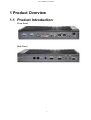
1 Product Overview
1.1 Product Introduction
Front Panel
Back Panel
5
LEC-7900D User Manual
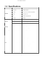
1.2 Specifications
FEATURE
DESCRIPTION
LEC-7900D
Form Factor
Embedded System
Processor
Intel Core 2 Duo, Celeron M (Socket P)
Chipset
Nvidia MCP7A-LP
BIOS
AMIBIOS with 8Mbit FWH
Max. FSB
1066MHz
Memory IC On Board
No
Memory Socket
SODIMM x 2 (up to 2GB per slot)
Max Memory
4GB (2GB Module x 2)
Compact Flash
CF Socket Type I/II x1
HDD
2.5” SATA HDD support
Networking
Controller (Interface)
RTL8111C(D) (PCIe 1X)
Video
Controller
Nvidia MCP7A-LP
Audio
Codec
ALC888 HD Codec
COM Ports
RS-232 x 1
DIO
4 Digital In, 4 Digital Out
USB 2.0
4 (External x 4)
Video Grabber / 3G / GPS
Video Grabber (Manufacture Option)
VGA
2 (1920 x 1440 / 75Hz)
DVI-D
UXGA (1600 x 1200)
HDMI
1 x (1.3 Mode 1920 x 1200)
LAN
RJ45 GbE x 2
Audio
Stereo Line out (RCA L/R)
Platform
Memory
Storage
I/O
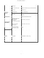
6
LEC-7900D User Manual
Hardware
Monitor
Internal CF
1
DC-in Connector Type
Phoenix Contact 2-pin, DC Jack (MP Version)
Expansion
Mini-PCIe x 1
Watchdog timer
Yes (1~255 level)
Controller
Winbond W83627 UHG integrated hardware
monitor
OS Supported
Environmental
Parameters
Dimensions
Power
Win XP-32bit/ Windows Vista
Operating Temperature
(With Industrial
Components:
CF, Memory, SSD, HDD)
-10°~55°C / 14°~131°F
Operating Temperature
(With Commercial
Components)
-5°C~45°C / 23°~113°F
Extended Operating
Temperature Tested
N/A
W x H x D (mm)
268(W) x 44(H) x 174(D)
W x H x D (Inch)
10.55”(W) x 1.73”(H) x 6.85”(D)
Input (Mode)
DC +12V (ATX Mode)
AC Adapter
AC Adapter D: 75W (+12V)
Compliance
Cooling
CE, FCC, RoHS
System Fan
1 x Smart FAN
7
LEC-7900D User Manual
2 System Components
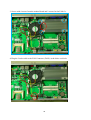
2.1 Block Diagram
8
LEC-7900D User Manual
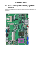
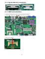
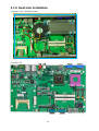
2.2 LEC-7900D(LEB-7900D) System
Board
LEB-7900D is the system board bundled with the LEC-7900D Fanless Embedded System
platform. The succeeding sections list LEB-7900D related jumper settings and connector pin
assignments.
9
LEC-7900D User Manual
10
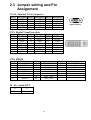
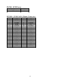
2.3 Jumper setting and Pin
Assignment
VGA1: Internal VGA Connector
Pin No. Description Pin No. Description Pin No. Description
1
CRT-R
6
GND
11
NC
2
CRT-G
7
GND
12
V_SDAT
3
CRT-B
8
GND
13
HSYNC
4
NC
9
VCC
14
VSYNC
5
GND
10
GND
15
V_SCLK
1
5
(DB-15 Female)
CN3: Digital Visual Interface
Pin No. Description Pin No. Description Pin No. Description
1
DATA29
DATA117
DATA02
DATA2+
10
DATA1+
18
DATA0+
3
GND
11
GND
19
GND
4
DATA412
DATA320
DATA55
DATA4+
13
DATA3+
21
DATA5+
6
DDC_CLK
14
VCC
22
GND
7
DDC_DAT
15
GND
23
CLK+
8
N.C
16
HP_DET
24
CLK-
CN4: HDMI
Pin No.
1
2
3
4
5
6
7
8
Description
TMDS Data 2+
SHIELD
TMDS Data 2TMDS Data 1+
SHIELD
TMDS Data 1TMDS Data 0+
SHIELD
Pin No.
9
10
11
12
13
14
15
16
Description
TMDS Data 0TMDS CLK+
SHIELD
TMDS CLKCEC
NC
DDC_CLK
DDC_DAT
J5 / J6 : Audio OUT
J5
J6
R-Channel
L-Channel
11
Pin No.
17
18
19
Description
GND
5V
HPD
LANB1 / LANB2
Pin No.
1
2
3
4
5
6
7
8
Description
Fast E-Net
Giga Net
TX+
MD0+
TXMD0RX+
MD1+
T45
MD2+
T45
MD2RXMD1T78
MD3+
T78
MD3-
RJ-45
DC1: DC Power Input
1
2
GND
+12VDC
LED1 : POWER HDD LED
1
2
POWER
HDD
PSW1 : Power Switch
PSW2 : Extern Power Buttom
USB1 / 2 : USB Dual Connector
PIN NO.
1
2
3
4
5
6
7
8
DESCRIPTION
USB_VCC
USBD0USBD0+
GND
USB_VCC
USBD1USBD1+
GND
12
5
8
1
4
USBB1
COM1: Internal COM1 ( D-SUB9) Connector
PIN NO.
1
2
3
4
5
6
7
8
9
DESCRIPTION
Data Carrier Detect ( DCDA # )
Receive Data ( RXDA )
Transmit Data ( TXDA )
Data Terminal Ready ( DTRA # )
Ground ( GND )
Data Set Ready ( DSRA # )
Request To Send ( RTSA # )
Clear To Send ( CTSA # )
Ring Indicator ( RIA # )
1
6
5
COM1
SC2T1 : Select COM1 Type
SC1T1
COM2 TYPE
SC1T2
RS-232 (Default)
RS-422
RS-485
1-2
3-4
5-6
SC1T3
1-5,2-6,3-7,4-8
5-9,6-10,7-11,8-12
5-9,6-10,7-11,8-12
5-6
J3: RS-232 Serial Port #2 Connector ( 2X5 Pin 2.54mm Header )
PIN NO.
1
2
3
4
5
6
7
8
9
10
DESCRIPTION
RS-232
Data Carrier Detect (DCDB #)
Data Set Ready (DSRB #)
Receive Data (RXDB)
Request To Send (RTSB #)
Transmit Data (TXDB)
Clear To Send (CTSB #)
Data Terminal Ready (DTRB #)
Ring Indicator (RIB #)
Ground
KEY
2
9
1
COM3
SATA 1 / 2 : SATA CONNECTOR
PIN NO.
1
2
3
4
5
6
7
10
DESCRIPTION
GND
TX+
TXGND
RXRX+
GND
13
9
CON1 : 4-Pin Power Connector (Small-4P )
Pin No.
1
2
3
4
Description
5V
Ground
Ground
12V
PS4S1
12 3 4
CN6 : Compact Flash Connector
PIN
1
2
3
4
5
6
7
8
9
10
11
12
13
14
15
16
17
18
19
20
21
22
23
24
25
DESCRIPTION
GND
DATA3
DATA4
DATA5
DATA6
DATA7
CE1#
A10
OE#
A9
A8
A7
CFVCC3
A6
A5
A4
A3
A2
A1
A0
DATA0
DATA1
DATA2
WP
CD2-
PIN
26
27
28
29
30
31
32
33
34
35
36
37
38
39
40
41
42
43
44
45
46
47
48
49
50
DESCRIPTION
CD1DATA11
DATA12
DATA13
DATA14
DATA15
CE2#
VS1#
IOR#
IOW#
WE#
READY#
CFVCC3
CSEL
VS2#
RESET
WAIT#
INPACK#
REG#
DASP#
DIAG#
DATA8
DATA9
DATA10
GND
J1:Clear CMOS Data
Description
Normal (Default)
Clear CMOS
CMOS1
1-2
2-3
J1
Normal (Default)
Clear CMOS1
1
2
3
1
2
3
1
2
3
14
50
25
CN6
26
1
JLCD1: LCD Power
Description
3.3V(Default)
5V
CMOS1
1-2
2-3
JLVDS1: LVDS 2x20 1.25mm Connector
Pin No.
1
3
5
7
9
11
13
15
17
19
21
23
25
27
29
31
33
35
37
39
Description
PVDD
LCD1D0#
LCD1D0
PVDD
LCD1D1#
LCD1D1
GND
LCD1D2#
LCD1D2
GND
LCD1D3#
LCD1D3
LCLK1#
LCLK1
ENBLD1
GND
ENBLD2
PVDD2
PVDD2
GND
Pin No.
2
4
6
8
10
12
14
16
18
20
22
24
26
28
30
32
34
36
38
40
Description
12V
LCD1D4#
LCD1D4
12V
LCD1D5#
LCD1D5
GND
LCD1D6#
LCD1D6
GND
LCD1D7#
LCD1D7
LCLK2#
LCLK2
BLCON
GND
BLCON2
GND
SPD1
SPCLK1
15
MPCI1:
:Mini-PCI Connector
Pin
1
3
5
7
9
11
13
15
17
19
21
23
25
27
29
31
33
35
37
39
41
43
45
47
49
51
53
55
57
59
61
Description
NC
NC
NC
NC
NC
NC
NC
NC
PIRQD#
VCC3
NC
GND
CK_33M_
GND
REQ#1
VCC3
A_D31
A_D29
GND
A_D27
A_D25
NC
C_BE#3
A_D23
GND
A_D21
A_D19
GND
A_D17
C_BE#2
IRDY#
Pin
63
65
67
69
71
73
75
77
79
81
83
85
87
89
91
93
95
97
99
101
103
105
107
109
111
113
115
117
119
121
123
Description
VCC3
TP
SERR#
GND
PERR#
C_BE#1
A_D14
GND
A_D12
A_D10
GND
A_D8
A_D7
VCC3
A_D5
NC
A_D3
VCC
A_D1
GND
NC
NC
NC
NC
NC
NC
NC
NC
NC
NC
VCC
16
Pin
2
4
6
8
10
12
14
16
18
20
22
24
26
28
30
32
34
36
38
40
42
44
46
48
50
52
54
56
58
60
62
Description
NC
NC
NC
NC
NC
NC
NC
NC
VCC
PIRQC#
NC
VCC3
PCI_RST#
VCC3
GNT#1
GND
PCI_PME#
NC
A_D30
VCC3
A_D28
A_D26
A_D24
MiniPCIDSEL
GND
A_D22
A_D20
PAR
A_D18
A_D16
GND
Pin
64
66
68
70
72
74
76
78
80
82
84
86
88
90
92
94
96
98
100
102
104
106
108
110
112
114
116
118
120
122
124
Description
FRAME#
TRDY#
STOP#
VCC3
DEVSEL#
GND
A_D15
A_D13
A_D11
GND
A_D9
C_BE#0
VCC3
A_D6
A_D4
A_D2
A_D0
NC
NC
GND
M66EN
NC
NC
NC
NC
GND
NC
NC
NC
NC
VCC3
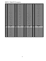
MPCIE1:
:Mini-PCIE Connector
Pin #
51
49
47
45
43
41
39
37
35
33
31
29
27
25
23
21
19
17
15
13
11
9
7
5
3
1
Signal Name
Pin #
Reserved
52
Reserved
50
Reserved
48
Reserved
46
Reserved
44
Reserved
42
Reserved
40
Reserved
38
GND
36
PETp0
34
PETn0
32
GND
30
GND
28
PERp0
26
PERn0
24
GND
22
Reserved (UIM_C4)
20
Reserved (UIM_C8)
18
Mechanical Key
GND
16
REFCLK+
14
REFCLK12
GND
10
CLKREQ#
8
Reserved
6
Reserved
4
WAKE#
2
17
Signal Name
+3.3V
GND
+1.5V
LED_WPAN#
LED_WLAN#
LED_WWAN#
GND
USB_D+
USB_DGND
SMB_DATA
SMB_CLK
+1.5V
GND
+3.3Vaux
PERST#
Reserved
GND
UIM_VPP
UIM_RESET
UIM_CLK
UIM_DATA
UIM_PWR
1.5V
GND
3.3V
3 Hardware Installation Guide
3.1 LEC-7900D Embedded System
LEC-7900D Embedded System Outlook
3.1.1 Begin Installation
Unscrew 8 thumbscrews of the chassis bottom cover and than remove the chassis bottom cover.
Note: For Safety reasons, please ensure that the power cord is disconnected before
opening the case.
18
3.1.2 System Memory Installation
Install the memory module into the socket and push it firmly down until it is fully seated.
3.1.3 SIM Card Installation
1. Remove the Rear panel in order to make room for SIM Card insertion.
2. SIM socket is located in the edge of main board (near to CF socket).
3. SIM card installation
19
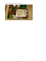
3.1.4 CompactFlash Card Installation
Carefully insert the CompactFlash card into the slot as shown in the illustration above.
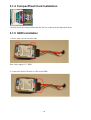
3.1.5 HDD Installation
1. Secure with 4 screws from the side
Note: Only support 2.5” HDD
2. Connect the Serial ATA/Power Cable to the HDD
20
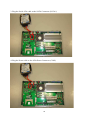
3. Plug the Serial ATA cable to the SATA Connector (SATA 1)
4. Plug the Power cable to the 4-Pin Power Connector (CON1)
21
5. Secure with 4 screws from the mother Board.
22
3.1.6 Heat sink Installation
1. Remove LEC-7900D Heat sink.
2. Install CPU
23
3. Secure with 4 screws from the mother Board and 2 screws for the FAN fix.
4. Plug the Cooler cable to the FAN Connector (FAN1) as the below red circle
24
3.1.7 Mini-PCIexpress Socket Installation
1. Mini-PCIexpress Socket for 3G mini-card module or WiFi mini-card module
3.1.8 System Complete
1. Replace the cover
2. Refasten the thumbscrews and than LEC-7900 Embedded System Installation Complete
Note: Please load the optimized BIOS values.
25
Appendix A. Watchdog Timer
Introduction
Most systems need to be self-reliant. If an error should occur it is typically not possible to
wait for the system to be rebooted manually. In some cases, such as apace probes, the system
is simply disabled. In other cases, the speed at which a human operator would reset the
system would be too slow to meet the uptime requirements of the product.
A watchdog timer is a piece of hardware that can be used to automatically detect system
anomalies and reset the processor if the case any problems are found. Generally speaking, a
watchdog timer is based on a counter that counts down from an initial value to zero. The
software selects the counter's initial value and periodically restarts it. Should the counter
reach zero before the software restarts it, the software is presumed to be malfunctioning and
the processor's reset signal is asserted. Thus, the processor will be restarted as if a human
operator had cycled the power
Watch Dog Sample code:
// Copyright (c) 2008 Lanner Electronic Inc. All rights reserved.
// Watchdog control utility for LEB-7900
#include
#include
#include
#include
#include
<stdio.h>
<string.h>
<dos.h>
<stdlib.h>
<inlines/pc.h>
#define INDEX_PORT
#define DATA_PORT
0x2e
0x2f
#define CR20_REG
0x20
#define W83627UHG_ID
//This register indicate the device's ID
0xA2
void help()
{
printf("Lanner Electronics Inc. 2009-05-22\n");
printf("Watchdog timer control V1.0 for LEB-7900\n\n");
printf("wdbp.exe -wr xxx (1-255 sec)(Watchdog Control - SYSTEM RESET)\n");
printf("\n");
}
int main(int argc, char *argv[])
{
int temp9 = 0;
int time;
if( argc < 2 )
{
help();
return -1;
}
//;********** Detect SIO ******************
Enter_Configuation();
if(detect_sio())
{
printf("It's not correct SuperIO, program terminated!!!\n");
temp9 = read_w83627UHG_reg(0, CR20_REG);
printf("Rx20 = %02X\n", temp9);
return -1;
}
Exit_Configuation();
Init_WDTO_GPIO_Interface();
//;********************* Setting Watchdog timer for System Reset
26
*****************************************************
if( strcmp(argv[1], "-wr") == 0 )
{
if( argc != 3 )
{
help();
return -1;
}
time = atoi(argv[2]);
printf("Setting Watchdog timer for System Reset...\n");
set_watchdog(time);
return 0;
}
else
{
help();
return -1;
}
return 0;
}
//;********************* set_watchdog
*****************************************************
int set_watchdog(int time)
{
int temp;
temp = time;
Enter_Configuation();
write_w83627UHG_reg(0x8, 0x30, 0x01);
//;enable LDN8
write_w83627UHG_reg(0x8, 0xf6, temp);
//LDN=8, CRF6, set watchdog
timer time-out value
Exit_Configuation();
return 0;
}
//;********************* Read SIO
*****************************************************
int read_w83627UHG_reg(int LDN, int reg)
{
outportb(INDEX_PORT, 0x07); //LDN register
delay(1);
outportb(DATA_PORT, LDN);
delay(1);
outportb(INDEX_PORT, reg);
delay(1);
return inportb(DATA_PORT);
}
//;********************* Write SIO
*****************************************************
int write_w83627UHG_reg(int LDN, int reg, int value)
{
outportb(INDEX_PORT, 0x07); //LDN register
delay(1);
outportb(DATA_PORT, LDN);
delay(1);
outportb(INDEX_PORT, reg);
delay(1);
outportb(DATA_PORT, value);
return 0;
}
//;********************* Enter SIO
*****************************************************
int Enter_Configuation()
{
outportb(INDEX_PORT, 0x87);
delay(1);
outportb(INDEX_PORT, 0x87);
27
}
return 0;
//;********************* Exit SIO
*****************************************************
int Exit_Configuation()
{
outportb(INDEX_PORT, 0xaa);
W83627THG Configuration
return 0;
}
//Exit
//;********************* Init WDTO and SB GPIO
*****************************************************
int Init_WDTO_GPIO_Interface()
{
Enter_Configuation();
write_w83627UHG_reg(0x8, 0x30, 0x01);
//;enable LDN8
write_w83627UHG_reg(0x8, 0xf5, 0x00);
//;//;set second
write_w83627UHG_reg(0x8, 0xf6, 0x00);
//;LDN=8, CRF6, stop timer first
write_w83627UHG_reg(0x8, 0xf7, 0x00);
Exit_Configuation();
}
//;clear status bit
return 0;
//input: none
//output: 1 = not correct SuperIO
//
0 = correct SuperIO
int detect_sio(void)
{
//check the SuperIO version
if(read_w83627UHG_reg(0,CR20_REG)==W83627UHG_ID)
return 0;
else
return 1;
}
28
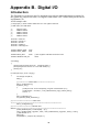
Appendix B. Digital I/O
Introduction
The Digitanl I/O on the rear panel is designed to provide the input and output operations for
the system For sample DIO code, see Digt-IO folder under LEC-7900D Utility on the Driver
and Manual CD.
A DIO sample code:
// Copyright (c) 2009 Lanner Electronic Inc. All rights reserved.
// DIO utility for LEB-7900
//;
//;
//;
//;
//;
Output
GPO30
GPO31
GPO32
GPO33
#include
#include
#include
#include
#include
Input
GPI34
GPI35
GPI36
GPI37
<stdio.h>
<string.h>
<dos.h>
<stdlib.h>
<inlines/pc.h>
#define INDEX_PORT
#define DATA_PORT
0x2e
0x2f
#define CR20_REG
0x20
#define W83627UHG_ID
//This register indicate the device's ID
0xA2
void help()
{
printf("Lanner Electronics Inc. 2009/10/28\n");
printf("Digital IO control V0.1 for LEB-7900\n");
printf("\n");
}
int main(int argc, char *argv[])
{
int temp6, temp8=0;
help();
//;********** Detect SIO ******************
Enter_Configuation();
if(detect_sio())
{
printf("It's not correct SuperIO, program terminated!!!\n");
printf("Rx20 = %02X\n", read_w83627UHG_reg(0, CR20_REG));
return -1;
}
Exit_Configuation();
Init_WDTO_GPIO_Interface();
//;********************* DIO start
*****************************************************
Enter_Configuation();
//;*********************GPO30 and
GPI34*****************************************************
printf("GPO30(OUT) to GPI34(IN)...\n");
write_w83627UHG_reg(0x07, 0xE1, read_w83627UHG_reg(0x07, 0xE1) | 0x01);
//;Set GPO30 to 1
delay(50);
for(temp6=1; temp6<50; temp6++)
29
{
gpio10:
temp8 = (read_w83627UHG_reg(0x07, 0xE1) >> 4) & 0x01;
//;Read GPI34=?
delay(50);
if(temp8 == 1)
{
printf("Write OUT GPO30=1 then IN GPI34=%2X \n",temp8);
goto gpio10;
}
}
printf("GPIO set HI error\n");
write_w83627UHG_reg(0x07, 0xE1, read_w83627UHG_reg(0x07, 0xE1) & ~0x01);
//;Set GPIO30 to 0
delay(50);
for(temp6=1; temp6<50; temp6++)
{
temp8 = (read_w83627UHG_reg(0x07, 0xE1) >> 4) & 0x01;
//;Read GPIO34=?
delay(50);
if(temp8 == 0)
{
printf("Write OUT GPO30=0 tnen IN GPI34=%2X \n",temp8);
goto gpio21;
}
}
printf("GPIO set LO error\n");
//;*********************GPO31 and
GPI35*****************************************************
gpio21:
printf("GPO31(OUT) to GPI35(IN)...\n");
write_w83627UHG_reg(0x07, 0xE1, read_w83627UHG_reg(0x07, 0xE1) | 0x02);
//;Set GPO31 to 1
delay(50);
for(temp6=1; temp6<50; temp6++)
{
temp8 = (read_w83627UHG_reg(0x07, 0xE1) >> 5) & 0x01;
//;Read GPI35=?
delay(50);
if(temp8 == 1)
{
printf("Write OUT GPO31=1 then IN GPI35=%2X \n",temp8);
goto gpio20;
}
}
printf("GPIO set HI error\n");
gpio20:
write_w83627UHG_reg(0x07, 0xE1, read_w83627UHG_reg(0x07, 0xE1) & ~0x02);
//;Set GPIO31 to 0
delay(50);
for(temp6=1; temp6<50; temp6++)
{
temp8 = (read_w83627UHG_reg(0x07, 0xE1) >> 5) & 0x01;
//;Read GPIO35=?
delay(50);
if(temp8 == 0)
{
printf("Write OUT GPO31=0 tnen IN GPI35=%2X \n",temp8);
goto gpio31;
}
}
printf("GPIO set LO error\n");
//;*********************GPO32 and
GPI36*****************************************************
gpio31:
printf("GPO32(OUT) to GPI36(IN)...\n");
write_w83627UHG_reg(0x07, 0xE1, read_w83627UHG_reg(0x07, 0xE1) | 0x04);
30
gpio30:
//;Set GPO32 to 1
delay(50);
for(temp6=1; temp6<50; temp6++)
{
temp8 = (read_w83627UHG_reg(0x07, 0xE1) >> 6) & 0x01;
//;Read GPI36=?
delay(50);
if(temp8 == 1)
{
printf("Write OUT GPO32=1 then IN GPI36=%2X \n",temp8);
goto gpio30;
}
}
printf("GPIO set HI error\n");
write_w83627UHG_reg(0x07, 0xE1, read_w83627UHG_reg(0x07, 0xE1) & ~0x04);
//;Set GPIO32 to 0
delay(50);
for(temp6=1; temp6<50; temp6++)
{
temp8 = (read_w83627UHG_reg(0x07, 0xE1) >> 6) & 0x01;
//;Read GPIO36=?
delay(50);
if(temp8 == 0)
{
printf("Write OUT GPO32=0 tnen IN GPI36=%2X \n",temp8);
goto gpio41;
}
}
printf("GPIO set LO error\n");
//;*********************GPO33 and
GPI37*****************************************************
gpio41:
printf("GPO33(OUT) to GPI37(IN)...\n");
write_w83627UHG_reg(0x07, 0xE1, read_w83627UHG_reg(0x07, 0xE1) | 0x08);
//;Set GPO33 to 1
delay(50);
for(temp6=1; temp6<50; temp6++)
{
temp8 = (read_w83627UHG_reg(0x07, 0xE1) >> 7) & 0x01;
//;Read GPI37=?
delay(50);
if(temp8 == 1)
{
printf("Write OUT GPO33=1 then IN GPI37=%2X \n",temp8);
goto gpio40;
}
}
printf("GPIO set HI error\n");
gpio40:
write_w83627UHG_reg(0x07, 0xE1, read_w83627UHG_reg(0x07, 0xE1) & ~0x08);
//;Set GPIO33 to 0
delay(50);
for(temp6=1; temp6<50; temp6++)
{
temp8 = (read_w83627UHG_reg(0x07, 0xE1) >> 7) & 0x01;
//;Read GPIO37=?
delay(50);
if(temp8 == 0)
{
printf("Write OUT GPO33=0 tnen IN GPI37=%2X \n",temp8);
goto _end;
}
}
printf("GPIO set LO error\n");
_end:
printf("Finish!!\n");
Exit_Configuation();
31
}
return 0;
//;********************* Read SIO
*****************************************************
int read_w83627UHG_reg(int LDN, int reg)
{
outportb(INDEX_PORT, 0x07); //LDN register
delay(1);
outportb(DATA_PORT, LDN);
delay(1);
outportb(INDEX_PORT, reg);
delay(1);
return inportb(DATA_PORT);
}
//;********************* Write SIO
*****************************************************
int write_w83627UHG_reg(int LDN, int reg, int value)
{
outportb(INDEX_PORT, 0x07); //LDN register
delay(1);
outportb(DATA_PORT, LDN);
delay(1);
outportb(INDEX_PORT, reg);
delay(1);
outportb(DATA_PORT, value);
return 0;
}
//;********************* Enter SIO
*****************************************************
int Enter_Configuation()
{
outportb(INDEX_PORT, 0x87);
delay(1);
outportb(INDEX_PORT, 0x87);
return 0;
}
//;********************* Exit SIO
*****************************************************
int Exit_Configuation()
{
outportb(INDEX_PORT, 0xaa);
W83627THG Configuration
return 0;
}
//Exit
//;********************* Init WDTO and SB GPIO
*****************************************************
int Init_WDTO_GPIO_Interface()
{
Enter_Configuation();
write_w83627UHG_reg(0x07, 0x30, 0x01);
//;enable GPIO3X
delay(5);
write_w83627UHG_reg(0x07, 0xE0, read_w83627UHG_reg(0x07, 0xE0) & 0xF0);
//Set GPIO30,31,32,33 to output
delay(5);
write_w83627UHG_reg(0x07, 0xE0, read_w83627UHG_reg(0x07, 0xE0) | 0xF0);
//Set GPIO34,35,36,37 to intput
delay(5);
Exit_Configuation();
}
return 0;
//input: none
//output: 1 = not correct SuperIO
32
//
0 = correct SuperIO
int detect_sio(void)
{
//check the SuperIO version
if(read_w83627UHG_reg(0,CR20_REG)==W83627UHG_ID)
return 0;
else
return 1;
}
33
Terms and Conditions
Date:2001.01.06
Warranty Policy :
1. All products are under warranty against defects in materials and workmanship
for a period of one year from the date of purchase.
2. The buyer will bear the return freight charges for goods returned for repair
within the warranty period; whereas the manufacturer will bear the after service
freight charges for goods returned to the user.
3. The buyer will pay for repair (for replaced components plus service time) and
transportation charges (both ways) for items after the expiration of the warranty
period.
4. If the RMA Service Request Form does not meet the stated requirement as
listed on “RMA Service,” RMA goods will be returned at customer’s expense.
5. The following conditions are excluded from this warranty:
Improper or inadequate maintenance by the customer
Unauthorized modification, misuse, or reversed engineering of the
product
Operation outside of the environmental specifications for the product.
RMA Service :
Requesting a RMA#
1. To obtain a RMA number, log on to the leRMA web interface at
http://erma.lannerinc.com . Use you user name and password as supplied to
you from your Lanner account manager.
2. Once you have logged on, follow the onscreen instructions to complete the
RMA process.
3. Ship the defective unit(s) on freight prepaid terms. Use the original packing
materials when possible.
4. Mark the RMA# clearly on the box.
Note: If you have any issues with the eRMA system, email
[email protected] for assistance.
34
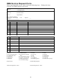
RMA Service Request Form
When requesting RMA service, please fill out the following form.
enclosed, your RMA cannot be processed.
Without this form
Company:
Reasons to Return: □ Repair (Please include failure details)
□ Testing Purpose
Contact Person:
Phone No.
Purchased Date:
Fax No.:
Applied Date:
RMA No:
Return Shipping Address:
Shipping by: □ Air Freight
□ Sea
□ Others:________________
Item Model Name
□ Express
Serial Number
Item Problem Code
*Problem Code:
01:D.O.A.
02: Second Time R.M.A.
03: CMOS Data Lost
04: FDC Fail
05: HDC Fail
06: Bad Slot
___
Configuration
Failure Status
07: BIOS Problem
08: Keyboard Controller
Fail
09: Cache RMA Problem
10: Memory Socket Bad
11: Hang Up Software
12: Out Look Damage
13: SCSI
14: LPT Port
15: PS2
16: LAN
17: COM Port
18: Watchdog Timer
Request Party
Confirmed By Supplier
Authorized Signatures / Date
Authorized Signatures / Date
35
19: DIO
20: Buzzer
21: Shut Down
22: Panel Fail
23: CRT Fail
24: Others (Pls specify)