1
MVME162
Embedded Controller
User’s Manual
(MVME162/D2)
Notice
While reasonable efforts have been made to assure the accuracy of this document,
Motorola, Inc. assumes no liability resulting from any omissions in this document, or
from the use of the information obtained therein. Motorola reserves the right to revise
this document and to make changes from time to time in the content hereof without
obligation of Motorola to notify any person of such revision or changes.
No part of this material may be reproduced or copied in any tangible medium, or
stored in a retrieval system, or transmitted in any form, or by any means, radio,
electronic, mechanical, photocopying, recording or facsimile, or otherwise, without the
prior written permission of Motorola, Inc.
It is possible that this publication may contain reference to, or information about
Motorola products (machines and programs), programming, or services that are not
announced in your country. Such references or information must not be construed to
mean that Motorola intends to announce such Motorola products, programming, or
services in your country.
Restricted Rights Legend
If the documentation contained herein is supplied, directly or indirectly, to the U.S.
Government, the following notice shall apply unless otherwise agreed to in writing by
Motorola, Inc.
Use, duplication, or disclosure by the Government is subject to restrictions as set forth
in subparagraph (c)(1)(ii) of the Rights in Technical Data and Computer Software
clause at DFARS 252.227-7013.
Motorola, Inc.
Computer Group
2900 South Diablo Way
Tempe, Arizona 85282
Preface
The MVME162 User’s Manual provides general information, hardware preparation and
installation instructions, operating instructions, and a functional description for the
MVME162 Embedded Controller.
This manual is intended for anyone who wants to design OEM systems, supply
additional capability to an existing compatible system, or work in a lab environment
for experimental purposes.
A basic knowledge of computers and digital logic is assumed.
To use this manual, you should be familiar with the publications listed in the Related
Documentation section in Chapter 1 of this manual.
The computer programs stored in the Read Only Memory of this device contain
material copyrighted by Motorola Inc., first published 1990, and may be used only
under a license such as the License for Computer Programs (Article 14) contained in
Motorola’s Terms and Conditions of Sale, Rev. 1/79.
!
WARNING
This equipment generates, uses, and can radiate radio
frequency energy and if not installed and used in
accordance with the documentation for this product, may
cause interference to radio communications. It has been
tested and found to comply with the limits for a Class A
Computing Device pursuant to Subpart J of Part 15 of FCC
rules, which are designed to provide reasonable protection
against such interference when operated in a commercial
environment. Operation of this equipment in a residential
area is likely to cause interference in which case the user, at
the user’s own expense, will be required to take whatever
measures necessary to correct the interference.
Motorola® and the Motorola symbol are registered trademarks of Motorola, Inc.
Delta SeriesTM, MC68040TM, VMEmoduleTM, VMEsystemTM, VMEexecTM, and 162BugTM
are trademarks of Motorola, Inc.
IndustryPackTM and IPTM are trademarks of GreenSpring Computers, Inc.
TimekeeperTM and ZeropowerTM are trademarks of Thompson Components.
All other products mentioned in this document are trademarks or registered
trademarks of their respective holders.
© Copyright Motorola 1993, 1994
All Rights Reserved
Printed in the United States of America
July 1994
Safety Summary
Safety Depends On You
The following general safety precautions must be observed during all phases of operation, service, and
repair of this equipment. Failure to comply with these precautions or with specific warnings elsewhere in
this manual violates safety standards of design, manufacture, and intended use of the equipment. Motorola,
Inc. assumes no liability for the customer’s failure to comply with these requirements.
The safety precautions listed below represent warnings of certain dangers of which Motorola is aware. You,
as the user of the product, should follow these warnings and all other safety precautions necessary for the
safe operation of the equipment in your operating environment.
Ground the Instrument.
To minimize shock hazard, the equipment chassis and enclosure must be connected to an electrical ground.
The equipment is supplied with a three-conductor AC power cable. The power cable must either be plugged
into an approved three-contact electrical outlet or used with a three-contact to two-contact adapter, with the
grounding wire (green) firmly connected to an electrical ground (safety ground) at the power outlet. The
power jack and mating plug of the power cable meet International Electrotechnical Commission (IEC) safety
standards.
Do Not Operate in an Explosive Atmosphere.
Do not operate the equipment in the presence of flammable gases or fumes. Operation of any electrical
equipment in such an environment constitutes a definite safety hazard.
Keep Away From Live Circuits.
Operating personnel must not remove equipment covers. Only Factory Authorized Service Personnel or
other qualified maintenance personnel may remove equipment covers for internal subassembly or
component replacement or any internal adjustment. Do not replace components with power cable
connected. Under certain conditions, dangerous voltages may exist even with the power cable removed. To
avoid injuries, always disconnect power and discharge circuits before touching them.
Do Not Service or Adjust Alone.
Do not attempt internal service or adjustment unless another person, capable of rendering first aid and
resuscitation, is present.
Use Caution When Exposing or Handling the CRT.
Breakage of the Cathode-Ray Tube (CRT) causes a high-velocity scattering of glass fragments (implosion).
To prevent CRT implosion, avoid rough handling or jarring of the equipment. Handling of the CRT should
be done only by qualified maintenance personnel using approved safety mask and gloves.
Do Not Substitute Parts or Modify Equipment.
Because of the danger of introducing additional hazards, do not install substitute parts or perform any
unauthorized modification of the equipment. Contact your local Motorola representative for service and
repair to ensure that safety features are maintained.
Dangerous Procedure Warnings.
Warnings, such as the example below, precede potentially dangerous procedures throughout this manual.
Instructions contained in the warnings must be followed. You should also employ all other safety
precautions which you deem necessary for the operation of the equipment in your operating environment.
!
WARNING
Dangerous voltages, capable of causing death, are present in
this equipment. Use extreme caution when handling,
testing, and adjusting.
Contents
CHAPTER 1
GENERAL INFORMATION
Introduction .............................................................................................................1-1
Models ......................................................................................................................1-1
Features.....................................................................................................................1-2
Specifications ...........................................................................................................1-3
Cooling Requirements.....................................................................................1-4
Special Considerations for Elevated Temperature Operation ...................1-4
FCC Compliance ..............................................................................................1-5
General Description ................................................................................................1-6
Input/Output ...................................................................................................1-6
VMEbus Interface ............................................................................................1-7
No-VMEbus-Interface Option........................................................................1-7
MCchip ..............................................................................................................1-7
Flash Memory and EPROM............................................................................1-7
IndustryPack Modules ....................................................................................1-8
Optional SCSI Interface...................................................................................1-8
Optional LAN Ethernet Transceiver Interface .............................................1-8
Required Equipment...............................................................................................1-8
MVME162Bug Firmware ................................................................................1-8
MVME712 Series Transition Modules...........................................................1-9
Available Software ...........................................................................................1-9
Related Documentation........................................................................................1-10
Support Information .............................................................................................1-11
Manual Terminology ............................................................................................1-12
vii
CHAPTER 2
HARDWARE PREPARATION AND INSTALLATION
Introduction .................................................................................................................2-1
Unpacking Instructions..............................................................................................2-1
Hardware Preparation ...............................................................................................2-1
SIM Selection ........................................................................................................2-2
Removal of Existing SIM .............................................................................2-4
Installation of New SIM ..............................................................................2-5
System Controller Select Header (J1)................................................................2-5
Synchronous Clock Select Header (J11) for Serial Port 1/Console ..............2-6
Clock Select Header (J12) for Serial Port 2 .......................................................2-6
SRAM Battery Backup Source Select Header (J20) .........................................2-7
EPROM Size Select Header (J21) .......................................................................2-7
General-Purpose Readable Jumpers Header (J22)..........................................2-8
Installation Instructions .............................................................................................2-9
IP Installation on the MVME162 .......................................................................2-9
MVME162 Module Installation .......................................................................2-10
System Considerations .....................................................................................2-12
CHAPTER 3
OPERATING INSTRUCTIONS
Introduction .................................................................................................................3-1
Switches and LEDs .....................................................................................................3-1
ABORT Switch (S1)..............................................................................................3-1
RESET Switch (S2) ...............................................................................................3-1
Front Panel Indicators (DS1 - DS4) ...................................................................3-2
Memory Maps .............................................................................................................3-3
Local Bus Memory Map .....................................................................................3-3
Normal Address Range ...............................................................................3-3
Detailed I/O Memory Maps ..............................................................................3-7
IPIC Overall Memory Map .......................................................................3-17
BBRAM, TOD Clock Memory Map .........................................................3-21
Interrupt Acknowledge Map....................................................................3-24
VMEbus Memory Map .....................................................................................3-24
VMEbus Accesses to the Local Bus..........................................................3-24
VMEbus Short I/O Memory Map............................................................3-24
Software Initialization ..............................................................................................3-24
Multi-MPU Programming Considerations ....................................................3-24
Local Reset Operation .......................................................................................3-25
viii
CHAPTER 4
FUNCTIONAL DESCRIPTION
Introduction ................................................................................................................ 4-1
MVME162 Functional Description .......................................................................... 4-1
Data Bus Structure .............................................................................................. 4-1
MC68040/MC68LC040 MPU ............................................................................ 4-2
EPROM and Flash Memory............................................................................... 4-2
SRAM.................................................................................................................... 4-2
About the Battery......................................................................................... 4-3
Onboard DRAM .................................................................................................. 4-4
Battery Backed Up RAM and Clock................................................................. 4-5
VMEbus Interface and VMEchip2 .................................................................... 4-5
I/O Interfaces ...................................................................................................... 4-5
Serial Communications Interface .............................................................. 4-5
IndustryPack (IP) Interfaces....................................................................... 4-8
Ethernet Interface......................................................................................... 4-8
SCSI Interface ............................................................................................... 4-9
SCSI Termination......................................................................................... 4-9
Local Resources ................................................................................................... 4-9
Programmable Tick Timers ...................................................................... 4-10
Watchdog Timer ........................................................................................ 4-10
Software-Programmable Hardware Interrupts..................................... 4-10
Local Bus Timeout ..................................................................................... 4-10
Timing Performance ......................................................................................... 4-10
Local Bus to DRAM Cycle Times ............................................................ 4-11
EPROM/Flash Cycle Times ..................................................................... 4-11
SCSI Transfers ............................................................................................ 4-11
LAN DMA Transfers................................................................................. 4-12
Remote Status and Control.............................................................................. 4-12
APPENDIX A
SERIAL INTERCONNECTIONS
Introduction ............................................................................................................... A-1
EIA-232-D Connections ............................................................................................ A-1
Interface Characteristics.................................................................................... A-3
EIA-530 Connections ................................................................................................ A-4
Interface Characteristics.................................................................................... A-6
Proper Grounding ..................................................................................................... A-8
ix
x
List of Figures
Figure 2-1. MVME162 Switch, Header, Connector, Fuse,
and LED Locations .............................................................................2-3
Figure 2-2. Serial Interface Module, Connector Side .........................................2-4
Figure 2-3. MVME162/MVME712M EIA-232-D Connection Diagram ........2-14
Figure 2-4. MVME162/MVME712x EIA-232-D Connection Diagram ..........2-20
Figure 2-5. MVME162 EIA-530 Connection Diagram......................................2-24
Figure 4-1. MVME162 Main Module Block Diagram ....................................4-13
Figure 4-2. Parity DRAM Mezzanine Module Block Diagram.......................4-14
xi
xii
List of Tables
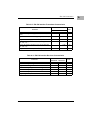
Table 1-1. MVME162 Models.................................................................................1-1
Table 1-2. MVME162 Specifications......................................................................1-3
Table 2-1. Serial Interface Module Part Numbers...............................................2-4
Table 3-1. Local Bus Memory Map .......................................................................3-4
Table 3-2. Local I/O Devices Memory Map ........................................................3-5
Table 3-3. VMEchip2 Memory Map......................................................................3-8
Table 3-4. MCchip Register Map .........................................................................3-14
Table 3-5. Z85230 SCC Register Addresses........................................................3-15
Table 3-6. 82596CA Ethernet LAN Memory Map.............................................3-15
Table 3-7. 53C710 SCSI Memory Map ................................................................3-16
Table 3-8. IPIC Overall Memory Map ................................................................3-17
Table 3-9. IPIC Memory Map—Control and Status Registers ........................3-18
Table 3-10. MK48T08 BBRAM/TOD Clock Memory Map..............................3-19
Table 3-11. BBRAM Configuration Area Memory Map...................................3-19
Table 3-12. TOD Clock Memory Map.................................................................3-20
Table 4-1. DRAM Performance............................................................................4-11
Table A-1. EIA-232-D Interconnections...............................................................A-2
Table A-2. EIA-232-D Interface Transmitter Characteristics ............................A-3
Table A-3. EIA-232-D Interface Receiver Characteristics .................................A-4
Table A-4. Serial Port B EIA-530 Interconnect Signals ......................................A-4
Table A-5. EIA-530 Interface Transmitter Characteristics ................................A-7
Table A-6. EIA-530 Interface Receiver Characteristics......................................A-7
xiii
xiv
GENERAL INFORMATION
1
Introduction
This manual provides general information, hardware preparation and
installation instructions, operating instructions, and a functional description
of the MVME162 Embedded Controller (referred to as the MVME162
throughout this manual).
Models
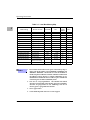
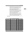
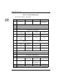
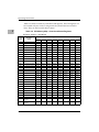
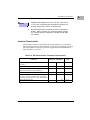
The MVME162 is available in several models, which are listed in Table 1-1.
Table 1-1. MVME162 Models
Model
Description
-001
MC68LC040 microprocessor, 1MB DRAM, 512KB SRAM
-002
MC68040 microprocessor, 1MB DRAM, 512KB SRAM
-003
MC68LC040 microprocessor, 1MB DRAM, 512KB SRAM, no VMEbus
-010
MC68LC040 microprocessor, 4MB DRAM, 512KB SRAM
-011
MC68LC040 microprocessor, 4MB DRAM, SCSI, 512KB SRAM
-012
MC68LC040 microprocessor, 4MB DRAM, Ethernet, 512KB SRAM
-013
MC68LC040 microprocessor, 4MB DRAM, SCSI, Ethernet, 512KB SRAM
-014
MC68LC040 microprocessor, 4MB DRAM, Ethernet, no VMEbus
-020
MC68040 microprocessor, 4MB DRAM, 512KB SRAM
-021
MC68040 microprocessor, 4MB DRAM, SCSI, 512KB SRAM
-022
MC68040 microprocessor, 4MB DRAM, Ethernet, 512KB SRAM
-023
MC68040 microprocessor, 4MB DRAM, SCSI, Ethernet, 512KB SRAM
-026
MC68040 microprocessor, 4MB DRAM, Ethernet, no VMEbus
-030
MC68LC040 microprocessor, 8MB DRAM, 512KB SRAM
-031
MC68LC040 microprocessor, 8MB DRAM, SCSI, 512KB SRAM
-032
MC68LC040 microprocessor, 8MB DRAM, Ethernet, 512KB SRAM
-033
MC68LC040 microprocessor, 8MB DRAM, SCSI, Ethernet, 512KB SRAM
-040
MC68040 microprocessor, 8MB DRAM, 512KB SRAM
-041
MC68040 microprocessor, 8MB DRAM, SCSI, 512KB SRAM
-042
MC68040 microprocessor, 8MB DRAM, Ethernet, 512KB SRAM
-043
MC68040 microprocessor, 8MB DRAM, SCSI, Ethernet, 512KB SRAM
MVME162/D21-1
1
General Information
Features
Features of the MVME162 include:
❏
25MHz 32-bit Microprocessor: either an MC68LC040 Enhanced 32-bit
Microprocessor with 8KB of cache and MMU, or an optional 25MHz
MC68040 32-bit Microprocessor with 8KB of cache, MMU, and FPU
❏
1MB, 4MB, or 8MB of shared Dynamic Random Access Memory (DRAM)
with programmable parity
❏
512KB of Static Random Access Memory (SRAM) with battery backup
❏
One JEDEC standard 32-pin PLCC EPROM socket (EPROMs may be
shipped separately from the MVME162)
❏
1MB Flash memory: either one Intel 28F008SA (for older boards) or four
Intel 28F020s (for newer boards)
❏
Four 32-bit programmable timers and programmable Watchdog Timer
(MCchip)
❏
Two 32-bit programmable timers and programmable Watchdog Timer
(optional VMEchip2)
❏
8K by 8 Non-Volatile Random Access Memory (NVRAM) and Time of
Day (TOD) clock with battery backup (Thompson MK48T08)
❏
Input/Output
❏
1-2
–
Two serial ports (one EIA-232-D DCE; one EIA-232-D or EIA-530
DCE/DTE)
–
Serial port controller (Zilog Z85230)
–
Optional Small Computer Systems Interface (SCSI) bus interface with
32-bit local bus burst Direct Memory Access (DMA) (NCR 53C710
controller)
–
Optional LAN Ethernet transceiver interface with 32-bit local bus
DMA (Intel 82596CA controller)
–
Four MVIP IndustryPack interfaces
VMEbus interface (VMEchip2)—non-VMEbus version optional
–
VMEbus system controller functions
–
VMEbus interface to local bus (A24/A32, D8/D16/D32
(D8/D16/D32/D64BLT) (BLT = Block Transfer)
–
Local bus to VMEbus interface (A16/A24/A32, D8/D16/D32)
–
VMEbus interrupter
MVME162 Embedded Controller User’s Manual
Specifications
❏
–
VMEbus interrupt handler
–
Global CSR for interprocessor communications
–
DMA for fast local memory-VMEbus transfers (A16/A24/A32,
D16/D32[D16/D32/D64BLT])
Switches and Light-Emitting Diodes (LEDs)
–
Two pushbutton switches (ABORT and RESET)
–
Eight LEDs (FAIL, STAT, RUN, SCON, LAN, FUSE, SCSI, and VME)
Specifications
Table 1-2, MVME162 Specifications, lists the specifications for an MVME162
without IndustryPacks. The subsequent sections detail cooling requirements
and FCC compliance.
Table 1-2. MVME162 Specifications
Characteristics
Power requirements
(with PROM; without IPs)
Specifications
+5V (± 5%), 3.5 A typical, 4.5 A maximum
+12 Vdc (± 5%), 100 mA maximum
-12 Vdc (± 5%), 100 mA maximum
Operating temperature
0° to 70° C exit air with forced air cooling (see NOTE)
Storage temperature
-40° to +85° C
Relative humidity
5% to 90% (noncondensing)
Physical dimensions
PC board with mezzanine
module only
Height
Depth
Thickness
Double-high VMEboard
PC board with connectors
and front panel
Height
Depth
Thickness
N ote
MVME162/D2
9.2 inches (233 mm)
6.3 inches (160 mm)
0.66 inch (17 mm)
10.3 inches (262 mm)
7.4 inches (188 mm)
0.80 inch (20.32 mm)
Refer to the following sections on Cooling Requirements and
Special Considerations for Elevated Temperature Operation.
1-3
1
1
General Information
Cooling Requirements
The Motorola MVME162 Embedded Controller is specified, designed, and
tested to operate reliably with an incoming air temperature range from 0° to
55° C (32° to 131° F) with forced air cooling at a velocity typically achievable
by using a 100 CFM axial fan. Temperature qualification is performed in a
standard Motorola VMEsystem 3000 chassis. Twenty-five watt load boards
are inserted in two card slots, one on each side, adjacent to the board under
test, to simulate a high power density system configuration. An assembly of
three axial fans, rated at 100 CFM per fan, is placed directly under the VME
card cage. The incoming air temperature is measured between the fan
assembly and the card cage, where the incoming airstream first encounters the
controller under test. Test software is executed as the controller is subjected to
ambient temperature variations. Case temperatures of critical, high power
density integrated circuits are monitored to ensure component vendors
specifications are not exceeded.
While the exact amount of airflow required for cooling depends on the
ambient air temperature and the type, number, and location of boards and
other heat sources, adequate cooling can usually be achieved with 10 CFM
and 490 LFM flowing over the controller. Less airflow is required to cool the
controller in environments having lower maximum ambients. Under more
favorable thermal conditions, it may be possible to operate the controller
reliably at higher than 55° C with increased airflow. It is important to note that
there are several factors, in addition to the rated CFM of the air mover, which
determine the actual volume and speed of air flowing over the controller.
Special Considerations for Elevated Temperature Operation
The following information is for users whose applications for the MVME162
may subject it to high temperatures.
The MVME162 uses commercial grade devices. Therefore, it can operate in an
environment with ambient air temperatures from 0° C to 70° C. Several factors
influence the ambient temperature seen by components on the MVME162.
Among them are inlet air temperature; air flow characteristics; number, types,
and locations of IndustryPack (IP) modules; power dissipation of adjacent
boards in the system, etc.
A temperature profile of the MVME162-023 was developed in an MVME945
12-slot VME chassis. This board was loaded with one GreenSpring IP-Dual
P/T module (position a) and three GreenSpring IP-488 modules (positions b,
c, and d). One twenty-five-watt load board was installed adjacent to each side
of the board under test. The exit air velocity was approximately 200 LFM
1-4
MVME162 Embedded Controller User’s Manual
Specifications
between the MVME162 and the IP-Dual P/T module. Under these conditions,
a 10° C rise between the inlet and exit air was observed. At 70° C exit air
temperature (60° C inlet air), the junction temperatures of devices on the
MVME162 were calculated (from the measured case temperatures) and did
not exceed 100° C.
C aution
For elevated-temperature operation, the user must perform
similar measurements and calculations to determine what
operating margin exists in a specific environment.
The following are some steps that the user can take to help make elevatedtemperature operation possible:
1.
Position the MVME162 board in the chassis for maximum airflow over the
component side of the board.
2.
Avoid placing boards with high power dissipation adjacent to the
MVME162.
3.
Use low-power IP modules only. The preferred locations for IP modules
are position a (J2 and J3) and position d (J18 and J19).
FCC Compliance
The MVME162 was tested without IndustryPacks in an FCC-compliant chassis
and meets the requirements for Class A equipment. FCC compliance was
achieved under the following conditions:
1.
Shielded cables on all external I/O ports.
2.
Cable shields connected to earth ground via metal shell connectors
bonded to a conductive module front panel.
3.
Conductive chassis rails connected to earth ground. This provides the
path for connecting shields to earth ground.
4.
Front panel screws properly tightened.
For minimum RF emissions, it is essential that the conditions above be
implemented. Failure to do so could compromise the FCC compliance of the
equipment containing the module.
MVME162/D2
1-5
1
1
General Information
General Description
The MVME162 is a double-high VMEmodule equipped with an MC68LC040
or optional MC68040 microprocessor. (The MC68040 microprocessor has a
floating-point coprocessor; the MC68LC040 does not.)
The MVME162 has 1MB, 4MB, or 8MB of parity-protected DRAM; 512KB
SRAM (with battery backup); a TOD clock (with battery backup); an optional
LAN Ethernet transceiver interface with DMA, two serial ports (EIA-232-D
and EIA-232-D/EIA-530); six tick timers with watchdog timer(s); optional
SCSI bus interface with DMA; VMEbus interface (local bus to
VMEbus/VMEbus to local bus, with A16/A24/A32, D8/D16/D32 bus widths
and a VMEbus system controller).
Input/Output
Input/Output (I/O) signals are routed through backplane connector P2. A P2
adapter board or LCP2 adapter board routes the signals and grounds from
connector P2 to an MVME712 series transition module (MVME712-12,
MVME712-13, MVME712A, MVME712AM, or MVME712M). The transition
module routes the signals to the appropriate configuration headers and
industry-standard connectors. Refer to the MVME712-12, MVME712-13,
MVME712A, MVME712AM, and MVME712B Transition Modules and LCP2
Adapter Board User’s Manual or the MVME712M Transition Module and P2
Adapter Board User’s Manual for more information.
N otes
When used with the MVME162, only serial ports 2 and 4 on
the MVME712 are available for use. Serial ports 1 and 3 and
the printer port are not connected to any MVME162 circuits
and should not be used.
An I/O device may be connected to serial port 1 (or 2) on the
MVME162 or to serial port 2 (or 4) on the MVME712, but not
both. (That is, if an I/O device is connected to MVME162
port 1, no other I/O device should be connected to
MVME712 port 2; they are functionally the same port.)
1-6
MVME162 Embedded Controller User’s Manual
General Description
VMEbus Interface
The optional VMEchip2 ASIC is the VMEbus interface for the MVME162.
(This option is a factory build and cannot be added in the field.) VMEchip2
features include:
❏
Two programmable 32-bit tick timers
❏
A programmable watchdog timer
❏
Programmable map decoders for the master and slave interfaces
❏
A VMEbus to/from local bus DMA controller
❏
A VMEbus to/from local bus non-DMA programmed access interface
❏
A VMEbus interrupter
❏
A VMEbus system controller
❏
A VMEbus interrupt handler
❏
A VMEbus requester
Processor-to-VMEbus transfers can be D8, D16, or D32. VMEchip2 DMA
transfers to the VMEbus, however, can be D16, D32, D16/BLT, D32/BLT, or
D64/MBLT.
No-VMEbus-Interface Option
If desired, the MVME162 can function as an embedded controller without a
VMEbus interface (i.e., without the optional VMEchip2). Contact your local
Motorola sales office for ordering information.
MCchip
The Memory Controller (MCchip) ASIC provides four 32-bit programmable
tick timers and an interface to the LAN chip, SCSI chip, serial port chip,
BBRAM, PROM/Flash, SRAM, DRAM, reset control, watchdog timers, access
timers, and interrupter logic.
Flash Memory and EPROM
The MVME162 is equipped with 1MB of Flash memory and an EPROM socket
ready for the installation of the EPROM, which may be ordered separately.
Flash memory is either a single device organized in a 1Mbit x 8 configuration
or four devices organized in a 256Kbit x 8 configuration. The EPROM location
is a standard JEDEC 32-pin PLCC capable of four Mbit densities (128 Kbit x 8;
MVME162/D2
1-7
1
1
General Information
256 Kbit x 8; 512 Kbit x 8; 1 Mbit x 8) organized as a 512Kbit x 8 device. A
jumper allows reset code to be fetched either from Flash memory or from the
EPROM.
IndustryPack Modules
Up to four IndustryPack (IP) modules may be installed on the MVME162. The
interface between the IPs and MVME162 is the IndustryPack Interface
Controller (IPIC) ASIC. Access to the IPs is provided by four 3M connectors
located behind the MVME162 front panel.
Optional SCSI Interface
An NCR 53C710 coprocessor provides the SCSI interface for the MVME162.
Optional LAN Ethernet Transceiver Interface
An Intel 82596CA controller provides the LAN Ethernet transceiver interface
for the MVME162.
Required Equipment
The following equipment is required to complete an MVME162 system:
N ote
❏
System console terminal
❏
Disk drives and controllers
❏
Operating system
❏
MVME712 series transition module (MVME712-12, MVME712-13,
MVME712A, MVME712AM, MVME712B, or MVME712M); P2 Adapter
Board or LCP2 Adapter Board; and cable
The MVME712B is an optional device used with MVME71212, MVME712-13, MVME712A, and MVME712AM modules
only.
MVME162Bug Firmware
The 162Bug package, MVME162BUG, is a powerful evaluation and debugging
tool for systems built around the MVME162 CISC-based microcomputers.
Facilities are available for loading and executing user programs under
complete operator control for system evaluation. 162Bug includes commands
for display and modification of memory, breakpoint and tracing capabilities,
a powerful assembler/disassembler useful for patching programs, and a self-
1-8
MVME162 Embedded Controller User’s Manual
Required Equipment
test at power-up feature which verifies the integrity of the system. Various
162Bug routines that handle I/O, data conversion, and string functions are
available to user programs through the TRAP #15 system calls.
N ote
MVME162Bug occupies the first half (512KB) of Flash
memory.
MVME712 Series Transition Modules
The MVME712 series transition modules provide an interface between the
MVME162 and peripheral devices such as EIA-232-D serial devices, SCSI
devices, and LAN Ethernet devices. A P2 Adapter Board or LCP2 Adapter
Board and cable are required.
C aution
Connect peripheral devices to MVME712 serial ports 2 and
4 only. (Serial port 2 is the terminal or bug interface.) Do
not connect peripheral devices to serial ports 1 and 3, or to
the printer port.
An I/O device may be connected to serial port 1 (or 2) on the
MVME162 or to serial port 2 (or 4) on the MVME712, but not
to both ports. (That is, if an I/O device is connected to
MVME162 port 1, no other I/O device should be connected
to MVME712 port 2; they are functionally the same port.)
Available Software
Available software for the MVME162 includes the on-board
debugger/monitor firmware, VMEexec driver packages for various
IndustryPack modules, and numerous third-party applications for MC680x0based systems. Contact your local Motorola sales office for more information.
MVME162/D2
1-9
1
1
General Information
Related Documentation
The following publications are applicable to the MVME162 and may provide
additional helpful information. If not shipped with this product, they may be
purchased by contacting your local Motorola sales office. Non-Motorola
documents may be purchased from the sources listed.
Document Title
M68040 Microprocessors User’s Manual
Motorola
Publication
Number
M68040UM
MVME162 Embedded Controller Support Information (Refer to SIMVME162
the Support Information section in this chapter)
MVME162Bug Debugging Package User’s Manual
MVME162BUG
Debugging Package for Motorola 68K CISC CPUs User’s
Manual, Parts 1 and 2
68KBUG1/2
Single Board Computers SCSI Software User’s Manual
SBCSCSI
MVME162 Embedded Controller Programmer’s Reference
Guide
MVME162PG
MVME712-12, MVME712-13, MVME712A, MVME712AM, and
MVME712B Transition Modules and LCP2 Adapter Board
User’s Manual
MVME712A
MVME712M Transition Module and P2 Adapter Board User’s
Manual
MVME712M
MVME1x7 Data Sheet Package (for use with the MVME162[LX]
and the MVME166/MVME167/MVME187)
N otes
68-1X7DS
Although not shown in the above list, each Motorola
Computer Group manual publication number is suffixed
with characters which represent the revision level of the
document, such as "/D2" (the second revision of a manual);
a supplement bears the same number as a manual but has a
suffix such as "/D2A1" (the first supplement to the second
edition of the manual).
The MVME1x7 Data Sheet Package is composed of vendorsupplied data sheets and manuals for the peripheral
controllers used on the MVME162 and other boards.
1-10
MVME162 Embedded Controller User’s Manual
Support Information
The following publications are available from the sources indicated.
Versatile Backplane Bus: VMEbus, ANSI/IEEE Std 1014-1987, The Institute of
Electrical and Electronics Engineers, Inc., 345 East 47th Street, New York, NY
10017 (VMEbus Specification). This is also available as Microprocessor system
bus for 1 to 4 byte data, IEC 821 BUS, Bureau Central de la Commission
Electrotechnique Internationale; 3, rue de Varembé, Geneva, Switzerland.
ANSI Small Computer System Interface-2 (SCSI-2), Draft Document X3.131-198X,
Revision 10c; Global Engineering Documents, P.O. Box 19539, Irvine, CA 92714.
IndustryPack Logic Interface Specification, Revision 1.0; GreenSpring Computers,
Inc., 1204 O’Brien Drive, Menlo Park, CA 94025.
82596CA Local Area Network Coprocessor data sheet, order number 290218; and
82596 User’s Manual, order number 296853; Intel Corporation, Literature
Sales, P.O. Box 58130, Santa Clara, CA 95052-8130.
NCR 53C710 SCSI I/O Processor Data Manual, order number NCR53C710DM;
and NCR 53C710 SCSI I/O Processor Programmer’s Guide, order number
NCR53C710PG; NCR Corporation, Microelectronics Products Division,
Colorado Springs, CO.
MK48T08(B) Timekeeper™ and 8Kx8 Zeropower™ RAM data sheet in Static
RAMs Databook, Order Code DBSRAM71; SGS-THOMPSON Microelectronics
Group; North & South American Marketing Headquarters, 1000 East Bell
Road, Phoenix, AZ 85022-2699.
Z85230 Serial Communications Controller data sheet, Zilog Inc., 210 Hacienda
Ave., Campbell, CA 95008-6609.
28F008SA Flash Memory Data Sheet, Order Number 290435-001; Intel Literature
Sales, P.O. Box 7641, Mt. Prospect, IL 60056-7641.
28F020 Flash Memory Data Sheet, Order Number 290245-003; Intel Literature
Sales, P.O. Box 7641, Mt. Prospect, IL 60056-7641.
Support Information
You can obtain connector interconnect signal information, parts lists, and
schematics for the MVME162 free of charge by contacting your local Motorola
sales office.
MVME162/D2
1-11
1
1
General Information
Manual Terminology
Throughout this manual, a convention is used which precedes data and
address parameters by a character identifying the numeric format as follows:
$
%
&
dollar
percent
ampersand
specifies a hexadecimal character
specifies a binary number
specifies a decimal number
Unless otherwise specified, all address references are in hexadecimal.
An asterisk (*) following the signal name for signals which are level-significant
denotes that the signal is true or valid when the signal is low.
An asterisk (*) following the signal name for signals which are edge-significant
denotes that the actions initiated by that signal occur on high-to-low
transition.
In this manual, assertion and negation are used to specify forcing a signal to a
particular state. In particular, assertion and assert refer to a signal that is active
or true; negation and negate indicate a signal that is inactive or false. These
terms are used independently of the voltage level (high or low) that they
represent.
In this manual, MVME712 series transition module refers generically to the
MVME712-12, MVME712-13, MVME712A, MVME712AM, or MVME712M.
MVME712x transition module refers to the closely related MVME712-12,
MVME712-13, MVME712A, or MVME712AM (not to the MVME712M).
References to a specific module use the complete designation of that module.
Data and address sizes are defined as follows:
1-12
❏
A byte is eight bits, numbered 0 through 7, with bit 0 being the least
significant.
❏
A word is 16 bits, numbered 0 through 15, with bit 0 being the least
significant.
❏
A longword is 32 bits, numbered 0 through 31, with bit 0 being the least
significant.
MVME162 Embedded Controller User’s Manual
HARDWARE PREPARATION
AND INSTALLATION
2
Introduction
This chapter provides unpacking instructions, hardware preparation
guidelines, and installation instructions for the MVME162 Embedded
Controller. Hardware preparation for the MVME712 series transition
modules is described in separate manuals; refer to the Related Documentation
section in Chapter 1.
Unpacking Instructions
N ote
If the shipping carton is damaged upon receipt, request that
the carrier’s agent be present during the unpacking and
inspection of the equipment.
Unpack the equipment from the shipping carton. Refer to the packing list and
verify that all items are present. Save the packing material for storing and
reshipping of equipment.
C aution
Avoid touching areas of integrated circuitry; static discharge
can damage circuits.
Hardware Preparation
To produce the desired configuration and ensure proper operation of the
MVME162, you may need to carry out certain modifications before installing
the module.
The MVME162 provides software control over most options: by setting bits in
control registers after installing the MVME162 in a system, you can modify its
configuration. (The MVME162 registers are described in Chapter 4, and/or in
the MVME162 Embedded Controller Programmer’s Reference Guide as listed in
Related Documentation in Chapter 1.)
Some options, however, are not software-programmable. Such options are
controlled by manual installation or removal of header jumpers or interface
modules.
MVME162/D22-1
Hardware Preparation and Installation
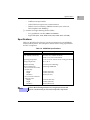
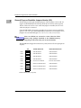
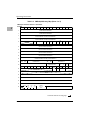
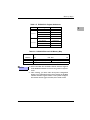
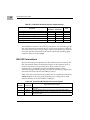
Figure 2-1 illustrates the placement of the switches, jumper headers,
connectors, and LED indicators on the MVME162. Manually configurable
items include:
2
❏
SIM selection for serial port B configuration (J10)
❏
System controller selection (J1)
❏
Synchronous clock selection (J11) for Serial Port 1/Console
❏
Synchronous clock selection (J12) for Serial Port 2
❏
SRAM backup power source selection (J20)
❏
EPROM size selection (J21)
❏
General-purpose readable register configuration (J22)
The MVME162 has been factory tested and is shipped with the configurations
described in the following sections. The MVME162’s required and factoryinstalled Debug Monitor, MVME162Bug (162Bug), operates with those factory
settings.
SIM Selection
Port B of the MVME162’s Z85230 serial communications controller is
configurable via a serial interface module (SIM) which is installed at connector
J10 on the MVME162 board. Four serial interface modules are available:
❏
EIA-232-D (DCE and DTE)
❏
EIA-530 (DCE and DTE)
You can change Port B from an EIA-232-D to an EIA-530 interface (or viceversa) by mounting the appropriate serial interface module. Port B is routed
(via the SIM at J10) to the 25-pin DB25 front panel connector marked SERIAL
PORT 2.
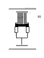
For the location of SIM connector J10 on the MVME162, refer to Figure 2-1.
Figure 2-2 illustrates the secondary side (bottom) of a serial interface module,
showing the J1 connector which plugs into SIM connector J10 on the
MVME162. Figure 2-3 (sheets 3-6), Figure 2-4 (sheets 3-4), and Figure 2-5
illustrate the configurations available for Port B.
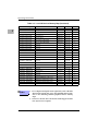
For the part numbers of the serial interface modules, refer to Table 2-1. The
part numbers are ordinarily printed on the primary side (top) of the SIMs, but
may be found on the secondary side in some versions.
If you need to replace an existing serial interface module with a SIM of another
type, go to Removal of Existing SIM below. If there is no SIM on the main board,
skip to Installation of New SIM.
2-2
MVME162 Embedded Controller User’s Manual
Hardware Preparation
2
P1
27
26
2
1
49
50
24
25
J8
27
26
2
1
A32
B32
C32
J3
A1
B1
C1
49
50
24
25
27
26
2
1
49
50
J6
1
2
F2
S1
2
1
S2
2
1
P3
40
39
P4
25
13
40
39
J10
PRIMARY SIDE
40
39
J9
A1
B1
C1
5 6
1 2
P2
27
26
2
1
J20
J14
1
A32
B32
C32
27
26
2
1
J21
J19
27
26
2
1
3
49
50
24
25
J18
1
2
49
50
24
25
49
50
24
25
J17
27
26
2
1
49
50
J13
J12 4
1
14
1
2
J15
J16
25
13
J11 4
1
SERIAL PORT 1/ CONSOLE
14
49
50
49
50
24
25
2
1
2
1 2
1
SERIAL PORT 2
J22
J7
1
2
F1
ABORT
cb232 9212
2-3
MVME162/D2
1
15
2
16
1
2
1
2
DS4
J5
19
20
RUN SCON
49
50
J4
DS3
49
50
24
25
SCSI VME
27
26
2
1
DS2
J2
DS1
49
50
24
25
FUSE
LAN
STAT
FAIL
J1
MVME
162-XX
RESET
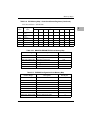
Figure 2-1. MVME162 Switch, Header, Connector, Fuse, and LED Locations
Hardware Preparation and Installation
2
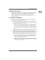
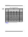
Table 2-1. Serial Interface Module Part Numbers
EIA
Standard
Configuration
Part Number
Model
Number
EIA-232-D
DTE
01-W3846B
SIM05
DCE
01-W3865B
SIM06
DTE
01-W3868B
SIM07
DCE
01-W3867B
SIM08
EIA-530
39
1
J1
40
2
SECONDARY SIDE
10922.00 9403 (2-2)
Figure 2-2. Serial Interface Module, Connector Side
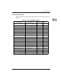
Removal of Existing SIM
1.
Each serial interface module is retained by two 4-40 x 3/16 ” Phillips-head
screws in opposite corners. Remove the two screws and store them in a
safe place for later use.
2.
Grasp opposite sides of the SIM and gently lift straight up.
C aution
3.
2-4
Avoid lifting the SIM by one side only, as the connector can
be damaged on the SIM or the main board.
Place the SIM in a static-safe container for possible reuse.
MVME162 Embedded Controller User’s Manual
Hardware Preparation
Installation of New SIM
1.
Observe the orientation of the connector keys on SIM connector J1 and
MVME162 connector J10. Turn the SIM so that the keys line up and place
it gently on connector J10, aligning the mounting holes at the SIM corners
with the matching standoffs on the MVME162.
2.
Gently press the top of the SIM to seat it on the connector. If the SIM does
not seat with gentle pressure, recheck the orientation. If the SIM connector
is oriented incorrectly, the mounting holes will not line up with the
standoffs.
C aution
3.
Do not attempt to force the SIM on if it is oriented incorrectly.
Place the two 4-40 x 3/16” Phillips-head screws that you previously
removed (or that were supplied with the new SIM) into the two oppositecorner mounting holes. Screw them into the standoffs but do not
overtighten them.
The signal relationships and signal connections in the various serial
configurations available for ports A and B are illustrated in Figures 2-3, 2-4,
and 2-5.
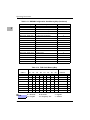
System Controller Select Header (J1)
The MVME162 is factory-configured as a VMEbus system controller (i.e., a
jumper is installed across pins 1 and 2 of header J1). Remove the J1 jumper if
the MVME162 is not to be the system controller. Note that when the
MVME162 is functioning as system controller, the SCON LED is turned on.
N ote
For MVME162s without the optional VMEbus interface (i.e.,
no VMEchip2), the jumper may be installed or removed
without affecting normal operation.
J1
J1
1
1
2
2
System Controller (factory configuration)
Not System Controller
MVME162/D2
2-5
2
Hardware Preparation and Installation
2
Synchronous Clock Select Header (J11) for Serial Port 1/Console
The MVME162 is shipped from the factory with the SERIAL PORT 1/CONSOLE
header configured for asynchronous communications (i.e., jumpers removed).
To select synchronous communications for the SERIAL PORT 1/CONSOLE
connection, install jumpers across pins 1 and 2 and pins 3 and 4.
J11
J11
2
4
1
3
Internal Clock (factory configuration)
2
4
1
3
External Clock
Clock Select Header (J12) for Serial Port 2
The MVME162 is shipped from the factory with the SERIAL PORT 2 header
configured for asynchronous communications (i.e., jumpers removed). To
select synchronous communications for the SERIAL PORT 2 connection, install
jumpers across pins 1 and 2 and pins 3 and 4.
J12
J12
2
4
1
3
Internal Clock (factory configuration)
2-6
2
4
1
3
External Clock
MVME162 Embedded Controller User’s Manual
Hardware Preparation
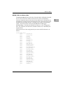
SRAM Battery Backup Source Select Header (J20)
2
The MVME162 is factory-configured to use VMEbus +5V standby power as a
backup power source for the SRAM (i.e., jumpers are installed across pins 1
and 3 and 2 and 4). To select the onboard battery as the backup power source,
install the jumpers across pins 3 and 5 and 4 and 6.
N ote
For MVME162s without the optional VMEbus interface (i.e.,
without the VMEchip2 ASIC), you must select the onboard
battery as the backup power source.
C aution
Removing all jumpers may temporarily disable the SRAM.
Do not remove all jumpers from J20, except for storage.
J20
J20
J20
1
2
1
2
1
2
5
6
5
6
5
6
VMEbus +5V STBY
(Factory configuration)
Backup Power Disabled
(For storage only)
Onboard Battery
EPROM Size Select Header (J21)
The MVME162 is factory-configured for a 4Mbit EPROM (i.e., a jumper is
installed across pins 2 and 3). This is the only size currently available; if a
larger EPROM becomes available, this jumper will allow it to be selected.
J21
1
2
3
4Mbit EPROM
(Factory configuration)
MVME162/D2
2-7
Hardware Preparation and Installation
2
General-Purpose Readable Jumpers Header (J22)
Header J22 provides eight readable jumpers. These jumpers can be read as a
register (at $FFF4202D) in the MCchip LCSR (local control/status register).
The bit values are read as a zero when the jumper is installed, and as a one
when the jumper is removed.
If the MVME162BUG firmware is installed, four jumpers are user-definable
(pins 1-2, 3-4, 5-6, 7-8). If the MVME162BUG firmware is not installed, seven
jumpers are user-definable (pins 1-2, 3-4, 5-6, 7-8, 11-12, 13-14, 15-16).
N ote
Pins 9-10 (GPIO3) are reserved to select either the Flash
memory map (jumper installed) or the EPROM memory
map (jumper removed). They are not user-definable.
The MVME162 is shipped from the factory with J22 set to all zeros (jumpers on
all pins).
J22
162BUG INSTALLED
USER CODE INSTALLED
USER-DEFINABLE
USER-DEFINABLE
GPIO6
USER-DEFINABLE
USER-DEFINABLE
GPIO5
USER-DEFINABLE
USER-DEFINABLE
GPIO4
USER-DEFINABLE
USER-DEFINABLE
IN=FLASH; OUT=EPROM
IN=FLASH; OUT=EPROM
GPIO2
REFER TO 162BUG MANUAL
USER-DEFINABLE
GPIO1
REFER TO 162BUG MANUAL
USER-DEFINABLE
REFER TO 162BUG MANUAL
USER-DEFINABLE
GPIO7
GPIO3
1
9
GPIO0 15
2
10
16
EPROMs Selected (factory configuration)
2-8
MVME162 Embedded Controller User’s Manual
Installation Instructions
Installation Instructions
2
The following sections discuss the installation of IndustryPacks (IPs) on the
MVME162, the installation of the MVME162 into a VME chassis, and the
system considerations relevant to the installation. Before installing
IndustryPacks, ensure that the serial ports and all header jumpers are
configured as desired.
IP Installation on the MVME162
Up to four IndustryPack (IP) modules may be installed on the MVME162.
Install the IPs on the MVME162 as follows:
1.
Each IP has two 50-pin connectors that plug into two corresponding 50pin connectors on the MVME162: J2/J3, J7/J8, J13/J14, J18/J19. See Figure
2-1 for the MVME162 connector locations.
–
2.
Orient the IP(s) so that the tapered connector shells mate properly.
Plug IP_a into connectors J2 and J3; plug IP_b into J7 and J8. Plug IP_c
into J13 and J14; plug IP_d into J18 and J19. If a double-sized IP is
used, plug IP_ab into J2, J3, J7, and J8; plug IP_cd into J13, J14, J18, and
J19.
Four additional 50-pin connectors (J6, J5, J17, and J16) are provided behind
the MVME162 front panel for external cabling connections to the IP
modules. There is a one-to-one correspondence between the signals on the
cabling connectors and the signals on the associated IP connectors (i.e., J6
has the same IP_a signals as J2; J5 has the same IP_b signals as J7; J17 has
the same IP_c signals as J13; and J16 has the same IP_d signals as J18.
–
Connect user-supplied 50-pin cables to J6, J5, J17, and J16 as needed.
Because of the varying requirements for each different kind of IP,
Motorola does not supply these cables.
–
Bring the IP cables out the narrow slots in the MVME162 front panel
and attach them to the appropriate external equipment, depending on
the nature of the particular IP(s).
MVME162/D2
2-9
Hardware Preparation and Installation
2
MVME162 Module Installation
With EPROM and IndustryPacks installed and headers properly configured,
proceed as follows to install the MVME162 in the VME chassis:
1.
Turn all equipment power OFF and disconnect the power cable from the
AC power source.
C aution
Inserting or removing modules while power is applied
could result in damage to module components.
!
Dangerous voltages, capable of causing death, are present in
this equipment. Use extreme caution when handling, testing, and adjusting.
WARNING
2-10
2.
Remove the chassis cover as instructed in the user’s manual for the
equipment.
3.
Remove the filler panel from the card slot where you are going to install
the MVME162.
–
If you intend to use the MVME162 as system controller, it must occupy
the leftmost card slot (slot 1). The system controller must be in slot 1
to correctly initiate the bus-grant daisy-chain and to ensure proper
operation of the IACK daisy-chain driver.
–
If you do not intend to use the MVME162 as system controller, it can
occupy any unused double-height card slot.
4.
Slide the MVME162 into the selected card slot. Be sure the module is
seated properly in the P1 and P2 connectors on the backplane. Do not
damage or bend connector pins.
5.
Secure the MVME162 in the chassis with the screws provided, making
good contact with the transverse mounting rails to minimize RF
emissions.
6.
Install the MVME712 series transition module in the front or the rear of the
VME chassis. (To install an MVME712M, which has a double-wide front
panel, you may need to shift other modules in the chassis.)
7.
On the chassis backplane, remove the INTERRUPT ACKNOWLEDGE
(IACK) and BUS GRANT (BG) jumpers from the header for the card slot
occupied by the MVME162.
MVME162 Embedded Controller User’s Manual
Installation Instructions
8.
Connect the P2 Adapter Board or LCP2 Adapter Board and cable(s) to
MVME162 backplane connector P2. This provides a connection point for
terminals or other peripherals at the EIA-232-D serial ports, SCSI ports,
and LAN Ethernet port.
For information on installing the P2 or LCP2 Adapter Board and the
MVME712 series transition module(s), refer to the manuals listed in
Related Documentation in Chapter 1 (the MVME162 Embedded Controller
Programmer’s Reference Guide provides some connection diagrams).
N ote
If you intend to use the MVME162 with Port B in an EIA-530
configuration, do not install the P2 or LCP2 Adapter Board
and the MVME712 series transition module. They are incompatible with the EIA-530 interface (refer to MVME162
Serial Port 2 in Chapter 4, Functional Description).
9.
Connect the appropriate cable(s) to the panel connectors for the EIA-232D serial ports, SCSI port, and LAN Ethernet port.
–
Note that some cables are not provided with the MVME712 series
module and must be made or purchased by the user. (Motorola
recommends shielded cable for all peripheral connections to minimize
radiation.)
10. Connect the peripheral(s) to the cable(s). Appendix A supplies detailed
information on the EIA-232-D signals supported. Appendix B describes
the Ethernet LAN (Local Area Network) port connections. Appendix C
describes the SCSI (Small Computer System Interface) I/O bus connections.
11. Install any other required VMEmodules in the system.
12. Replace the chassis cover.
13. Connect the power cable to the AC power source and turn the equipment
power ON.
MVME162/D2
2-11
2
Hardware Preparation and Installation
2
System Considerations
The MVME162 draws power from VMEbus backplane connectors P1 and P2.
P2 is also used for the upper 16 bits of data in 32-bit transfers, and for the upper
8 address lines in extended addressing mode. The MVME162 may not function
properly without its main board connected to VMEbus backplane connectors
P1 and P2.
Whether the MVME162 operates as a VMEbus master or as a VMEbus slave, it
is configured for 32 bits of address and 32 bits of data (A32/D32). However, it
handles A16 or A24 devices in the address ranges indicated in Chapter 3. D8
and/or D16 devices in the system must be handled by the MC68040/
MC68LC040 software. Refer to the memory maps in Chapter 3.
The MVME162 contains shared onboard DRAM whose base address is
software-selectable. Both the onboard processor and offboard VMEbus
devices see this local DRAM at base physical address $00000000, as
programmed by the MVME162Bug firmware. This may be changed via
software to any other base address. Refer to the MVME162 Embedded Controller
Programmer’s Reference Guide for more information.
If the MVME162 tries to access offboard resources in a nonexistent location and
is not system controller, and if the system does not have a global bus timeout,
the MVME162 waits forever for the VMEbus cycle to complete. This will cause
the system to lock up. There is only one situation in which the system might
lack this global bus timeout: when the MVME162 is not the system controller
and there is no global bus timeout elsewhere in the system.
Multiple MVME162s may be installed in a single VME chassis. In general,
hardware multiprocessor features are supported.
N ote
If you are installing multiple MVME162s in an MVME945
chassis, do not install an MVME162 in slot 12. The height of
the IP modules may cause clearance difficulties in that slot
position.
Other MPUs on the VMEbus can interrupt, disable, communicate with, and
determine the operational status of the processor(s). One register of the GCSR
(global control/status register) set includes four bits that function as location
monitors to allow one MVME162 processor to broadcast a signal to any other
MVME162 processors. All eight registers are accessible from any local
processor as well as from the VMEbus.
2-12
MVME162 Embedded Controller User’s Manual
Installation Instructions
The MVME162 provides +5 Vdc power to the remote LED/switch connector
(J4) through a 1A fuse (F1) located near J4. Connector J4 is the interface for a
remote control and indicator panel. If none of the LEDs light and the ABORT
and RESET switches do not operate, check fuse F1.
The MVME162 provides +12 Vdc power to the Ethernet transceiver interface
through a 1A fuse (F2) located near diode CR1. The FUSE LED lights to indicate
that +12 Vdc is available. When the MVME712M module is used, the yellow
DS1 LED on the MVME712M illuminates when LAN power is available, which
indicates that the fuse is good. If the Ethernet transceiver fails to operate, check
fuse F2.
The MVME162 provides SCSI terminator power through a 1A fuse (F1) located
on the P2 Adapter Board or LCP2 Adapter Board. If the fuse is blown, the SCSI
device(s) may function erratically or not at all. When the P2 Adapter Board is
used with an MVME712M and the SCSI bus is connected to the MVME712M,
the green DS2 LED on the MVME712M front panel illuminates when SCSI
terminator power is available. If the green DS2 LED flickers during SCSI bus
operation, check P2 Adapter Board fuse F1.
MVME162/D2
2-13
2
Hardware Preparation and Installation
2
712M TRANSITION
MODULE
PORT 2
DB25
TO MODEM
J17
RXD
TXD
CTS
RTS
DCD
DTR
P2-C27
TXD2
TXD
P2-C28
RXD2
RXD
P2-C29
RTS2
RTS
P2-C30
CTS2
CTS
P2-C31
DTR2
DTR
P2-C32
DCD2
DCD
DSR
P2
TXC
CABLE
TO TERMINAL
J16
PIN 2
PIN 3
PIN 4
PIN 5
PIN 20
PIN 8
PIN 6
PIN 15
RXC
PIN 17
TXCO
+12V
PIN 24
PIN 7
1.5K
MVME 712M EIA- 232-D DTE CONFIGURATION (TO MODEM)
FRONT PANEL
DB25
Z85230
A PORT
D
TXD
R
RXD
D
RTS
R
CTS
D
DTR
R
DCD
D
TXC
TXD
RXD
RTS
CTS
DTR
DCD
DSR
TXC
RXC
D
3
1
4
2
D
R
RXC
TXCO
PIN 2
PORT 1
PIN 3
PIN 4
PIN 5
PIN 20
PIN 8
PIN 6
MVME162 EIA-232-D DCE CONFIGURATION
(TO TERMINAL)
PIN 15
PIN 17
PIN 24
J11
PIN 7
10970.00 (1-6) 9405
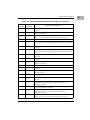
Figure 2-3. MVME162/MVME712M EIA-232-D Connection Diagram (Sheet 1 of 6)
2-14
MVME162 Embedded Controller User’s Manual
Installation Instructions
2
712M TRANSITION
MODULE
PORT 2
RXD
TXD
CTS
RTS
DCD
DTR
TO MODEM
J17
DB25
P2-C27
TXD2
TXD
P2-C28
RXD2
RXD
P2-C29
RTS2
RTS
P2-C30
CTS2
CTS
P2-C31
DTR2
DTR
P2-C32
DCD2
DCD
DSR
P2
TXC
CABLE
TO TERMINAL
J16
PIN 2
PIN 3
PIN 4
PIN 5
PIN 20
PIN 8
PIN 6
PIN 15
RXC
PIN 17
TXCO
+12V
PIN 24
PIN 7
1.5K
MVME712M EIA-232-D DCE CONFIGURATION (TO TERMINAL)
FRONT PANEL
DB25
Z85230
A PORT
D
TXD
R
RXD
D
RTS
R
CTS
D
DTR
R
DCD
D
TXC
TXD
RXD
RTS
CTS
DTR
DCD
DSR
TXC
RXC
D
3
1
4
2
D
R
RXC
TXCO
PIN 2
PORT 1
PIN 3
PIN 4
PIN 5
PIN 20
PIN 8
PIN 6
MVME162 EIA-232-D DCE CONFIGURATION
(TO TERMINAL)
PIN 15
PIN 17
PIN 24
J11
PIN 7
10970.00 (2-6) 9405
Figure 2-3. MVME162/MVME712M EIA-232-D Connection Diagram (Sheet 2 of 6)
MVME162/D2
2-15
Hardware Preparation and Installation
2
712M TRANSITION
MODULE
PORT 4
TO MODEM
J19
TXD
RXD
RTS
CTS
DTR
DCD
DB25
P2-A25
TXD4
TXD
P2-A26
RXD4
RXD
P2-A27
RTS4
RTS
P2-A29
CTS4
CTS
P2-A30
DTR4
DTR
P2-A31
DCD4
DCD
DSR
P2-A32
RTXC4
TXC
TRXC P2-A28
TRXC4
RXC
RTXC
P2
TO TERMINAL
J18
CABLE
TXCO
PIN 2
PIN 3
PIN 4
PIN 5
PIN 20
PIN 8
PIN 6
PIN 15
PIN 17
PIN 24
PIN 7
+12V
1.5K
J15
MVME712M EIA-232-D DTE CONFIGURATION (TO MODEM)
NOTE: WITH DTE MODULE, THE RECEIVE CLOCK OF 85230 ON B INTERFACE
MUST BE PROGRAMMED AS INPUT TO PREVENT BUFFER CONTENTION
SIM05
EIA-232-D DTE
Z85230
FRONT PANEL
DB25
B PORT
TXD
RXD
R
RTS
RTS
D
CTS
CTS
R
DTR
DTR
D
DCD
DCD
R
NC
TXC
RXC
TXD
D
RXD
3
4
1
2
J12
DSR
TXC
R
+5V
R
D
RXC
TXCO
PIN 2
PORT 2
PIN 3
PIN 4
PIN 5
PIN 20
PIN 8
PIN 6
MVME 162 EIA-232-D DTE CONFIGURATION
(TO MODEM)
PIN 15
PIN 17
PIN 24
PIN 7
10970.00 (3-6) 9405
Figure 2-3. MVME162/MVME712M EIA-232-D Connection Diagram (Sheet 3 of 6)
2-16
MVME162 Embedded Controller User’s Manual
Installation Instructions
2
712M TRANSITION
MODULE
PORT 4
TO MODEM
J19
TXD
RXD
RTS
CTS
DTR
DCD
DB25
P2-A25
TXD4
TXD
P2-A26
RXD4
RXD
P2-A27
RTS4
RTS
P2-A29
CTS4
CTS
P2-A30
DTR4
DTR
P2-A31
DCD4
DCD
DSR
P2-A32
RTXC4
TXC
TRXC P2-A28
TRXC4
RXC
RTXC
P2
TO TERMINAL
J18
TXCO
CABLE
PIN 2
PIN 3
PIN 4
PIN 5
PIN 20
PIN 8
PIN 6
PIN 15
PIN 17
PIN 24
PIN 7
+12V
1.5K
J15
MVME712M EIA-232-D DCE CONFIGURATION (TO TERMINAL)
SIM06
EIA-232-D DCE
Z85230
FRONT PANEL
DB25
B PORT
TXD
RXD
R
RTS
RTS
D
CTS
CTS
R
DTR
DTR
D
DCD
DCD
R
D
TXC
RXC
TXD
D
RXD
3
4
1
2
J12
+5V
DSR
TXC
D
D
R
RXC
TXCO
PIN 2
PORT 2
PIN 3
PIN 4
PIN 5
PIN 20
PIN 8
PIN 6
MVME 162 EIA-232-D DCE CONFIGURATION
(TO TERMINAL)
PIN 15
PIN 17
PIN 24
PIN 7
10970.00 (4-6) 9405
Figure 2-3. MVME162/MVME712M EIA-232-D Connection Diagram (Sheet 4 of 6)
MVME162/D2
2-17
Hardware Preparation and Installation
2
712M TRANSITION
MODULE
PORT 4
TXD
RXD
RTS
CTS
DTR
DCD
TO MODEM
J19
DB25
TXD
P2-A25
TXD4
P2-A26
RXD4
RXD
P2-A27
RTS4
RTS
P2-A29
CTS4
CTS
P2-A30
DTR4
DTR
P2-A31
DCD4
DCD
DSR
RTXC
P2-A32
TRXC P2-A28
TXC
RTXC4
TO TERMINAL
J18
TRXC4
CABLE
PIN 3
PIN 4
PIN 5
PIN 20
PIN 8
PIN 6
PIN 15
RXC
PIN 17
TXCO
P2
PIN 2
PIN 24
PIN 7
+12V
1.5K
J15
MVME712M EIA-232-D CONFIGURATION (TO TERMINAL)
NOTES:
1. WITH DTE MODULE AND MVME 712 JUMPERED AS TO TERMINAL,
THE CLOCKS (TXC AND RXC) ARE THE WRONG DIRECTION.
THE CLOCKS ARE BOTH INPUTS. THEY SHOULD BOTH BE OUTPUTS.
2. WITH DTE MODULE, THE RECEIVE CLOCK OF 85230 ON B INTERFACE
MUST BE PROGRAMMED AS INPUT TO PREVENT BUFFER CONTENTION.
SIM05
EIA-232-D DTE
Z85230
FRONT PANEL
DB25
B PORT
TXD
RXD
R
RTS
RTS
D
CTS
CTS
R
DTR
DTR
D
DCD
DCD
R
NC
TXC
RXC
TXD
D
RXD
3
4
1
2
J12
DSR
TXC
R
+5V
R
D
RXC
TXCO
PIN 2
PORT 2
PIN 3
PIN 4
PIN 5
PIN 20
PIN 8
PIN 6
MVME 162 EIA-232-D DTE CONFIGURATION
(TO MODEM)
PIN 15
PIN 17
PIN 24
PIN 7
10970.00 (5-6) 9405
Figure 2-3. MVME162/MVME712M EIA-232-D Connection Diagram (Sheet 5 of 6)
2-18
MVME162 Embedded Controller User’s Manual
Installation Instructions
2
712M TRANSITION
MODULE
PORT 4
TXD
RXD
RTS
CTS
DTR
DCD
TO MODEM
J19
DB25
TXD
P2-A25
TXD4
P2-A26
RXD4
RXD
P2-A27
RTS4
RTS
P2-A29
CTS4
CTS
P2-A30
DTR4
DTR
P2-A31
DCD4
DCD
DSR
RTXC
P2-A32
TRXC P2-A28
TXC
RTXC4
TO TERMINAL
J18
TRXC4
PIN 3
PIN 4
PIN 5
PIN 20
PIN 8
PIN 6
PIN 15
RXC
PIN 17
TXCO
P2
PIN 2
PIN 24
CABLE
PIN 7
+12V
1.5K
J15
MVME712M EIA-232-D DTE CONFIGURATION (TO MODEM)
NOTE:
WITH DCE MODULE AND MVME 712 JUMPERED AS TO TERMINAL,
THE CLOCKS (TXC AND RXC) ARE THE WRONG DIRECTION.
THE CLOCKS ARE BOTH OUTPUTS. THEY SHOULD BOTH BE INPUTS.
SIM06
EIA-232-D DCE
Z85230
FRONT PANEL
DB25
B PORT
TXD
RXD
R
RTS
D
RTS
CTS
R
CTS
DTR
D
DTR
DCD
R
DCD
D
TXC
RXC
TXD
D
RXD
3
4
1
2
J12
+5V
DSR
TXC
D
D
R
RXC
TXCO
PIN 2
PORT 2
PIN 3
PIN 4
PIN 5
PIN 20
PIN 8
PIN 6
MVME 162 EIA-232-D DCE CONFIGURATION
(TO TERMINAL)
PIN 15
PIN 17
PIN 24
PIN 7
10970.00 (6-6) 9405
Figure 2-3. MVME162/MVME712M EIA-232-D Connection Diagram (Sheet 6 of 6)
MVME162/D2
2-19
Hardware Preparation and Installation
2
712A/AM/12/13
TRANSITION MODULE
PORT 2
DCE
1.5K
DTE
J9
1.5K
+12V
SERIAL PORT 2
J16
RXD
TXD
CTS
RTS
DCD
DTR
DB9
P2-C27
TXD2
TXD
P2-C28
RXD2
RXD
P2-C29
RTS2
RTS
P2-C30
CTS2
CTS
P2-C31
DTR2
DTR
P2-C32
DCD2
DCD
DSR
P2
CABLE
MODEM PORT 2
J17
PIN 3
PIN 2
PIN 7
PIN 8
PIN 4
PIN 1
PIN 6
MTXD
RJ11
MRXD
MCTS
MDTR
MODEM
(712AM/712-13
ONLY)
TIP
RING
PIN 2
PIN 3
MDCD
MVME 712A/AM/-12/-13 PORT 2 CONFIGURED AS EIA-232-D SERIAL PORT
NOTES:
1. SERIAL PORT 2 IS HARD-WIRED DTE. USE NULL MODEM CABLE FOR DCE.
2. TO CONNECT TERMINAL, SET DSR LINE PULLUP SELECT J9 TO "DCE".
FRONT PANEL
DB25
Z85230
A PORT
D
TXD
R
RXD
D
RTS
R
CTS
D
DTR
R
DCD
TXC
D
RXC
D
TXD
RXD
RTS
CTS
DTR
DCD
DSR
TXC
3
1
4
2
D
R
RXC
TXCO
PIN 2
PORT 1
PIN 3
PIN 4
PIN 5
PIN 20
PIN 8
PIN 6
MVME162 RS232 DCE CONFIGURATION
(TO TERMINAL)
PIN 15
PIN 17
PIN 24
J11
PIN 7
11020.00 9406 (1-4)
Figure 2-4. MVME162/MVME712x EIA-232-D Connection Diagram (Sheet 1 of 4)
2-20
MVME162 Embedded Controller User’s Manual
Installation Instructions
2
712AM/13
TRANSITION MODULE
PORT 2
DCE
1.5K
DTE
J9
1.5K
+12V
SERIAL PORT 2
J16
RXD
TXD
CTS
RTS
DCD
DTR
DB9
P2-C27
TXD2
TXD
P2-C28
RXD2
RXD
P2-C29
RTS2
RTS
P2-C30
CTS2
CTS
P2-C31
DTR2
DTR
P2-C32
DCD2
DCD
DSR
P2
CABLE
PIN 3
PIN 2
PIN 7
PIN 8
PIN 4
PIN 1
PIN 6
MODEM PORT 2
J17
MTXD
RJ11
MRXD
MCTS
MDTR
TIP
MODEM
(712AM/712-13
ONLY)
RING
PIN 2
PIN 3
MDCD
MVME 712AM/-13 PORT 2 CONFIGURED AS MODEM
NOTE:
USING SERIAL PORT 2 AS A MODEM PORT REQUIRES CONNECTION TO
+5/+12/-12Vdc BACKPLANE POWER, A DATA CABLE AT THE DB9 CONNECTOR,
AND A TELCO CABLE AT THE RJ11 CONNECTOR. REFER TO THE USER’S
MANUAL FOR THIS MODULE (MVME712A) FOR SETUP INSTRUCTIONS.
FRONT PANEL
DB25
Z85230
A PORT
D
TXD
R
RXD
D
RTS
R
CTS
D
DTR
R
DCD
TXC
D
RXC
D
TXD
RXD
RTS
CTS
DTR
DCD
DSR
TXC
3
1
4
2
D
R
RXC
TXCO
PIN 2
PORT 1
PIN 3
PIN 4
PIN 5
PIN 20
PIN 8
PIN 6
MVME162 RS232 DCE CONFIGURATION
(TO TERMINAL)
PIN 15
PIN 17
PIN 24
J11
PIN 7
11020.00 9406 (2-4)
Figure 2-4. MVME162/MVME712x EIA-232-D Connection Diagram (Sheet 2 of 4)
MVME162/D2
2-21
Hardware Preparation and Installation
2
712A/AM/-12/-13
TRANSITION MODULE
PORT 4
DCE
1.5K
DTE
J14
1.5K
+12V
DB9
TXD
RXD
RTS
CTS
DTR
DCD
P2-A25
TXD4
TXD
P2-A26
RXD4
RXD
P2-A27
RTS4
RTS
P2-A29
CTS4
CTS
P2-A30
DTR4
DTR
P2-A31
DCD4
DCD
DSR
TXC
P2-A32
RTXC4
RXC P2-A28
TRXC4
P2
PIN 3
PIN 2
PIN 7
PIN 8
PIN 4
PIN 1
PIN 6
NC
NC
CABLE
MVME 712A/AM/-12/-13 PORT 4 (DTE)
NOTES:
1. SERIAL PORT 4 IS HARD-WIRED DTE. USE NULL MODEM CABLE FOR DCE.
2. TO CONNECT TERMINAL, SET DSR LINE PULLUP SELECT J14 TO "DCE".
SIM05
EIA-232-D DTE
Z85230
FRONT PANEL
DB25
B PORT
TXD
RXD
R
RTS
RTS
D
CTS
CTS
R
DTR
DTR
D
DCD
DCD
R
NC
TXC
RXC
TXD
D
RXD
3
4
1
2
J12
DSR
TXC
R
+5V
R
D
RXC
TXCO
PIN 2
PORT 2
PIN 3
PIN 4
PIN 5
PIN 20
PIN 8
PIN 6
MVME 162 RS232 DTE CONFIGURATION
(TO MODEM)
PIN 15
PIN 17
PIN 24
PIN 7
11020.00 9406 (3-4)
Figure 2-4. MVME162/MVME712x EIA-232-D Connection Diagram (Sheet 3 of 4)
2-22
MVME162 Embedded Controller User’s Manual
Installation Instructions
2
712A/AM/-12/-13
TRANSITION MODULE
PORT 4
DCE
DTE
1.5K
J14
1.5K
+12V
DB9
TXD
RXD
RTS
CTS
DTR
DCD
P2-A25
TXD4
TXD
P2-A26
RXD4
RXD
P2-A27
RTS4
RTS
P2-A29
CTS4
CTS
P2-A30
DTR4
DTR
P2-A31
DCD4
DCD
DSR
TXC
P2-A32
RTXC4
RXC P2-A28
TRXC4
P2
PIN 3
PIN 2
PIN 7
PIN 8
PIN 4
PIN 1
PIN 6
NC
NC
CABLE
MVME 712A/AM/-12/-13 PORT 4 (DTE)
NOTES:
1. SERIAL PORT 4 IS HARD-WIRED DTE. USE NULL MODEM CABLE FOR DCE.
2. TO CONNECT TERMINAL, SET DSR LINE PULLUP SELECT J14 TO "DCE".
SIM06
EIA-232-D DCE
Z85230
FRONT PANEL
DB25
B PORT
TXD
RXD
R
RTS
RTS
D
CTS
CTS
R
DTR
DTR
D
DCD
DCD
R
D
TXC
RXC
TXD
D
RXD
3
4
1
2
+5V
J12
DSR
TXC
D
D
R
RXC
TXCO
PIN 2
PORT 2
PIN 3
PIN 4
PIN 5
PIN 20
PIN 8
PIN 6
MVME 162 RS232 DCE CONFIGURATION
(TO TERMINAL)
PIN 15
PIN 17
PIN 24
PIN 7
11020.00 9406 (4-4)
Figure 2-4. MVME162/MVME712x EIA-232-D Connection Diagram (Sheet 4 of 4)
MVME162/D2
2-23
Hardware Preparation and Installation
2
P2 CONNECTOR
TXD_B
TXD_A
RXD_B
RXD_A
RTS_B
RTS_A
CTS_B
CTS_A
DTR_B
DTR_A
DCD_B
DCD_A
DSR_B
MVME 162 EIA-530 DTE CONFIGURATION
(TO MODEM)
DSR_A
TXC_B
TXC_A
RXC_B
RXC_A
TXCO_B
TXCO_A
TM_A
LL_A
RL_A
SIM07
EIA-530 DTE
Z85230
TXD
RTS_B
RTS_A
D
RTS
CTS
CTS_B
CTS_A
R
DTR_B
DTR_A
D
DTR
DCD
TXC
RXC
RXD_B
RXD_A
R
RXD
NC
3
R
DCD_B
DCD_A
R
DSR_B
DSR_A
R
TXC_B
TXC_A
4
+5V
1
RXC_B
RXC_A
2
R
J12
TXCO_B
TXCO_A
D
NC
+5V
D
+5V
D
P2-A26
P2-C19
P2-A27
P2-C26
P2-A29
P2-A23
P2-A30
P2-C22
P2-A31
P2-A22
P2-A20
P2-C24
P2-A32
P2-C21
P2-A28
P2-C23
P2-A24
P2-C25
P2-C20
P2-A21
PIN 1
TXD_B
TXD_A
D
P2-A25
P2-A19
FRONT PANEL
DB 25
NC
B PORT
P2-C18
TM_A
LL_A
RL_A
PIN 14
PIN 2
PORT
2
PIN 16
PIN 3
PIN 18
PIN 4
PIN 13
PIN 5
PIN 23
PIN 20
PIN 10
PIN 8
PIN 22
PIN 6
PIN 12
PIN 15
PIN 9
PIN 17
PIN 11
PIN 24
PIN 25
PIN 19
PIN 21
PIN 7
NOTE: SUFFIX _A = THE + SIGNAL.
SUFFIX _B = THE - SIGNAL.
10971.00 (1-2) 9405
Figure 2-5. MVME162 EIA-530 Connection Diagram (Sheet 1 of 2)
2-24
MVME162 Embedded Controller User’s Manual
Installation Instructions
2
P2 CONNECTOR
TXD_B
TXD_A
RXD_B
RXD_A
RTS_B
RTS_A
CTS_B
CTS_A
DTR_B
DTR_A
DCD_B
DCD_A
DSR_B
MVME 162 EIA-530 DCE CONFIGURATION
(TO TERMINAL)
DSR_A
TXC_B
TXC_A
RXC_B
RXC_A
TXCO_B
TXCO_A
TM_A
LL_A
RL_A
SIM08
EIA-530 DCE
Z85230
TXD
RXD_B
RXD_A
R
RXD
RTS_B
RTS
RTS_A
D
CTS
CTS_B
CTS_A
R
DTR
DTR_B
DTR_A
D
DCD_B
DCD_A
R
DCD
TXC
3
RXC
D
DSR_B
DSR_A
D
TXC_B
TXC_A
D
RXC_B
RXC_A
4
+5V
1
2
J12
TXCO_B
R
+5V
TXCO_A
TM_A
D
NC
NC
P2-A26
P2-C19
P2-A27
P2-C26
P2-A29
P2-A23
P2-A30
P2-C22
P2-A31
P2-A22
P2-A20
P2-C24
P2-A32
P2-C21
P2-A28
P2-C23
P2-A24
P2-C25
P2-C20
P2-A21
PIN 1
TXD_B
TXD_A
D
P2-A25
P2-A19
FRONT PANEL
DB 25
NC
B PORT
P2-C18
LL_A
RL_A
PORT
2
PIN 14
PIN 2
PIN 16
PIN 3
PIN 18
PIN 4
PIN 13
PIN 5
PIN 23
PIN 20
PIN 10
PIN 8
PIN 22
PIN 6
PIN 12
PIN 15
PIN 9
PIN 17
PIN 11
PIN 24
PIN 25
PIN 19
PIN 21
PIN 7
7
PIN
NOTE: SUFFIX _A = THE + SIGNAL.
SUFFIX_-B = THE - SIGNAL.
10971.00 (2-2) 9405
Figure 2-5. MVME162 EIA-530 Connection Diagram (Sheet 2 of 2)
MVME162/D2
2-25
Hardware Preparation and Installation
2
2-26
MVME162 Embedded Controller User’s Manual
OPERATING
INSTRUCTIONS
3
Introduction
This chapter provides information necessary to use the MVME162 in a system
configuration. This includes a description of the switches and LEDs, memory
maps, and software initialization of the module.
Switches and LEDs
The MVME162 front panel has ABORT and RESET switches and eight LED
(light-emitting diode) indicators (FAIL, STAT, RUN, SCON, LAN, FUSE, SCSI,
VME).
ABORT Switch (S1)
When enabled by software, the ABORT switch generates an interrupt at a userprogrammable level. It is normally used to abort program execution and
return to the 162Bug debugger firmware located in the MVME162 EPROM
and Flash memory.
The ABORT switch interrupter in the MCchip ASIC is an edge-sensitive
interrupter connected to the ABORT switch. This interrupter is filtered to
remove switch bounce.
RESET Switch (S2)
The RESET switch resets all onboard devices; it also drives SYSRESET* if the
MVME162 is the system controller. The RESET switch may be disabled by
software.
The VMEchip2 includes both a global and a local reset driver. When the
VMEchip2 operates as the VMEbus system controller, the reset driver
provides a global system reset by asserting the VMEbus signal SYSRESET*. A
SYSRESET* may be generated by the RESET switch, a power-up reset, a
watchdog timeout, or by a control bit in the LCSR in the VMEchip2. SYSRESET*
remains asserted for at least 200 ms, as required by the VMEbus specification.
Similarly, the VMEchip2 provides an input signal and a control bit to initiate
a local reset operation. By setting a control bit, software can maintain a board
in a reset state, disabling a faulty board from participating in normal system
operation. The local reset driver is enabled even when the VMEchip2 is not the
MVME162/D23-1
Operating Instructions
system controller. A local reset may be generated by the RESET switch, a
power-up reset, a watchdog timeout, a VMEbus SYSRESET*, or a control bit in
the GCSR.
3
N ote
For an MVME162 without the VMEbus option (i.e., with no
VMEchip2), the LCSR control bit is not available to reset the
module. In this case, the watchdog timer is allowed to time
out to reset the MVME162.
Front Panel Indicators (DS1 - DS4)
There are eight LEDs on the MVME162 front panel: FAIL, STAT, RUN, SCON,
LAN, FUSE, SCSI, and VME.
❏
FAIL LED (red). Lights when the BRDFAIL* signal line is active. Part of
DS1.
❏
STAT LED (yellow). Driven by the MC68040 status lines on the MVME162.
Lights when a halt condition from the processor is detected. Part of DS1.
❏
RUN LED (green). Lights when the local bus TIP* signal line is low. This
indicates one of the local bus masters is executing a local bus cycle. Part of
DS2.
❏
SCON LED (green). Lights when the VMEchip2 in the MVME162 is the
VMEbus system controller. Part of DS2.
❏
LAN LED (green). Lights when the LAN chip is local bus master. Part of
DS3.
❏
FUSE LED (green). Lights when power is available to the transceiver
interface (the MVME162 supplies +12V power to the LAN Ethernet
transceiver interface through a fuse). Part of DS3.
❏
SCSI LED (green). Lights when the SCSI chip is local bus master. Part of
DS4.
❏
3-2
VME LED (green). Lights when the board is using the VMEbus (VMEbus
AS* line asserted by the VMEchip2) or when the board is accessed by the
VMEbus (VMEchip2 is the local bus master). Part of DS4.
User’s Manual
Memory Maps
Memory Maps
There are two points of view for memory maps:
❏
The mapping of all resources as viewed by local bus masters (local bus
memory map)
❏
The mapping of onboard resources as viewed by VMEbus masters
(VMEbus memory map)
3
Local Bus Memory Map
The local bus memory map is split into different address spaces by the
Transfer Type (TT) signals. The local resources respond to the normal access
and interrupt acknowledge codes.
Normal Address Range
The memory map of devices that respond to the normal address range is
shown in the following tables. The normal address range is defined by the TT
signals on the local bus. For the MVME162, transfer types 0, 1, and 2 define the
normal address range. Table 3-1 defines the entire map ($00000000 to
$FFFFFFFF). Many areas of the map are user-programmable, and suggested
uses are shown in the table. The cache inhibit function is programmable in the
MC68xx040 MMU. The onboard I/O space must be marked ‘‘cache inhibit’’
and serialized in its page table. Table 3-2 further defines the map for the local
I/O devices.
MVME162/D2
3-3
Operating Instructions
Table 3-1. Local Bus Memory Map
3
Address Range
Devices Accessed
Port Width
Size
Software
Cache
Inhibit
Notes
Programmable
DRAM on Board
D32
1MB-8MB
N
2
Programmable
SRAM
D32
128KB-2MB
N
2
Programmable
VMEbus A32/A24
D32/D16
--
?
4
Programmable
IP_a Memory
D32-D8
64 KB-8 MB
?
2, 4
Programmable
IP_b Memory
D32-D8
64 KB-8 MB
?
2, 4
Programmable
IP_c Memory
D32-D8
64 KB-8 MB
?
2, 4
Programmable
IP_d Memory
D32-D8
64 KB-8 MB
?
2, 4
$FF800000-$FF9FFFFF
Flash/EPROM
D32
2 MB
N
1, 5
$FFA00000-$FFBFFFFF
EPROM/Flash
D32
2 MB
N
6
$FFC00000-$FFCFFFFF
Not Decoded
D32
1 MB
N
7
$FFD00000-$FFDFFFFF
Not Decoded
D32
1 MB
N
7
$FFE00000-$FFE7FFFF
SRAM default
D32
512 KB
N
--
$FFE80000-$FFEFFFFF
Not Decoded
$FFF00000-$FFFEFFFF
Local I/O Devices
(Refer to next table)
$FFFF0000-$FFFFFFFF
VMEbus A16
N otes
--
512 KB
N
7
D32-D8
878 KB
Y
3
D32/D16
64 KB
?
2, 4
1. Reset enables the decoder for this space of the memory map so
that it will decode address spaces $FF800000 - $FF9FFFFF and
$00000000 - $003FFFFF. The decode at 0 must be disabled in
the MCchip before DRAM is enabled. DRAM is enabled with
the DRAM Control Register at address $FFF42048, bit 24.
PROM/Flash is disabled at the low address space with PROM
Control Register at address $FFF42040, bit 20.
2. This area is user-programmable. The DRAM and SRAM
decoder is programmed in the MCchip, the local-to-VMEbus
decoders are programmed in the VMEchip2, and the IP
memory space is programmed in the IPIC.
3. Size is approximate.
4. Cache inhibit depends on devices in area mapped.
3-4
User’s Manual
Memory Maps
5. The EPROM and Flash are sized by the MCchip ASIC from an
8-bit private bus to the 32-bit MPU local bus. Because the
device size is less than the allocated memory map for some
entries, the device contents repeat for those entries.
3
If jumper GPIO3 is installed, the Flash device is accessed. If
GPIO3 is not installed, the EPROM is accessed.
6. The Flash and EPROM are sized by the MCchip ASIC from an
8-bit private bus to the 32-bit MPU local bus. Because the
device size is less than the allocated memory map for some
entries, the device contents repeat for those entries.
If jumper GPIO3 is installed, the PROM device is accessed. If
GPIO3 is not installed, the Flash is accessed.
7. These areas are not decoded unless one of the programmable
decoders are initialized to decode this space. If they are not
decoded, an access to this address range will generate a local
bus timeout. The local bus timer must be enabled.
Table 3-2 focuses on the ‘‘Local I/O Devices’’ portion of the local bus main
memory map.
Table 3-2. Local I/O Devices Memory Map
Address Range
Devices Accessed
Port Width
Size
--
256 KB
Notes
$FFF00000 - $FFF3FFFF
Reserved
$FFF40000 - $FFF400FF
VMEchip2 (LCSR)
D32
256 B
4
$FFF40100 - $FFF401FF
VMEchip2 (GCSR)
D32-D8
$FFF40200 - $FFF40FFF
Reserved
$FFF41000 - $FFF41FFF
$FFF42000 - $FFF42FFF
$FFF43000 - $FFF44FFF
$FFF45000 - $FFF45800
$FFF45801 - $FFF45FFF
SCC #2 (Z85230)
D8
2 KB
1, 2
$FFF46000 - $FFF46FFF
LAN (82596CA)
D32
4 KB
1, 6
1, 3
256 B
1, 3
--
3.5 KB
4, 5
Reserved
--
4 KB
4
MCchip
D32-D8
4 KB
1
Reserved
--
8 KB
4
SCC #1 (Z85230)
D8
2 KB
1, 2
$FFF47000 - $FFF47FFF
SCSI (53C710)
$FFF48000 - $FFF57FFF
Reserved
D32-D8
4 KB
1
--
64 KB
4
$FFF58000 - $FFF5807F
IPIC IP_a I/O
D16
128 B
1
$FFF58080 - $FFF580FF
IPIC IP_a ID
D16
128 B
1
$FFF58100 - $FFF5817F
IPIC IP_b I/O
D16
128 B
1
$FFF58180 - $FFF581FF
IPIC IP_b ID Read
D16
128 B
1
$FFF58200 - $FFF5827F
IPIC IP_c I/O
D16
128 B
1
MVME162/D2
3-5
Operating Instructions
Table 3-2. Local I/O Devices Memory Map (Continued)
Address Range
3
Devices Accessed
Port Width
Size
Notes
$FFF58280 - $FFF582FF
IPIC IP_c ID
D16
128 B
$FFF58300 - $FFF5837F
IPIC IP_d I/O
D16
128 B
1
1
$FFF58380 - $FFF583FF
IPIC IP_d ID Read
D16
128 B
1
$FFF58400 - $FFF584FF
IPIC IP_ab I/O
D32-D16
256 B
1
$FFF58500 - $FFF585FF
IPIC IP_cd I/O
D32-D16
256 B
8
$FFF58600 - $FFF586FF
IPIC IP_ab I/O Repeated
D32-D16
256 B
1
$FFF58700 - $FFF587FF
IPIC IP_cd I/O Repeated
D32-D16
256 B
8
$FFF58800 - $FFF5887F
Reserved
--
128 B
1
$FFF58880 - $FFF588FF
Reserved
--
128 B
1
$FFF58900 - $FFF5897F
Reserved
--
128 B
1
$FFF58980 - $FFF589FF
Reserved
--
128 B
1
$FFF58A00 - $FFF58A7F
Reserved
--
128 B
1
$FFF58A80 - $FFF58AFF
Reserved
--
128 B
1
$FFF58B00 - $FFF58B7F
Reserved
--
128 B
1
$FFF58B80 - $FFF58BFF
Reserved
--
128 B
1
$FFF58C00 - $FFF58CFF
Reserved
--
256 B
1
$FFF58D00 - $FFF58DFF
Reserved
--
256 B
1
$FFF58E00 - $FFF58EFF
Reserved
--
256 B
1
$FFF58F00 - $FFF58FFF
Reserved
--
256 B
1
$FFFBC000 - $FFFBC01F
IPIC Registers
D32-D8
2 KB
1
$FFFBC800 - $FFFBC81F
Reserved
--
2 KB
1
$FFFBD000 - $FFFBFFFF
Reserved
--
12 KB
4
$FFFC0000 - $FFFC7FFF
MK48T08 (BBRAM, TOD Clock)
D32-D8
32 KB
1
$FFFC8000 - $FFFCBFFF
MK48T08 & Disable Flash writes
D32-D8
16 KB
1, 7
$FFFCC000 - $FFFCFFFF
MK48T08 & Enable Flash writes
D32-D8
16 KB
1, 7
$FFFD0000 - $FFFEFFFF
Reserved
--
128 KB
4
N otes
1. For a complete description of the register bits, refer to the data
sheet for the specific chip. For a more detailed memory map,
refer to the following detailed peripheral device memory
maps.
2. The SCC is an 8-bit device located on an MCchip private data
bus. Byte access is required.
3-6
User’s Manual
Memory Maps
3. Writes to the LCSR in the VMEchip2 must be 32 bits. LCSR
writes of 8 or 16 bits terminate with a TEA signal. Writes to the
GCSR may be 8, 16 or 32 bits. Reads to the LCSR and GCSR
may be 8, 16 or 32 bits. Byte reads should be used to read the
interrupt vector.
3
4. This area does not return an acknowledge signal. If the local
bus timer is enabled, the access times out and is terminated by
a TEA signal.
5. Size is approximate.
6. Port commands to the 82596CA must be written as two 16-bit
writes: upper word first and lower word second.
7. Refer to the Flash and EPROM Interface section in the MCchip
description in Chapter 3.
Detailed I/O Memory Maps
Tables 3-3 through 3-12 provide detailed memory maps for the VMEchip2, the
MCchip, the Zilog Z85230 serial communications controller, the Intel 82596CA
LAN controller, the NCR 53C710 SCSI controller, the IPIC chip, and the
MK48T08 BBRAM/TOD Clock.
MVME162/D2
3-7
Operating Instructions
Table 3-3. VMEchip2 Memory Map (Sheet 1 of 3)
VMEchip2 LCSR Base Address = $FFF40000
OFFSET:
31
3
30
29
28
27
26
25
24
23
22
21
0
SLAVE ENDING ADDRESS 1
4
SLAVE ENDING ADDRESS 2
8
SLAVE ADDRESS TRANSLATION ADDRESS 1
C
19
18
17
16
SLAVE ADDRESS TRANSLATION ADDRESS 2
ADDER
2
10
31
30
29
28
27
SNP
2
26
25
WP
2
SUP
2
USR
2
A32
2
A24
2
BLK
D64
2
BLK
2
PRGM
2
DATA
2
24
23
22
21
20
19
18
17
16
14
MASTER ENDING ADDRESS 1
18
MASTER ENDING ADDRESS 2
1C
MASTER ENDING ADDRESS 3
20
MASTER ENDING ADDRESS 4
MASTER ADDRESS TRANSLATION ADDRESS 4
24
28
20
MAST
D16
EN
MAST
WP
EN
MAST
D16
EN
MASTER AM 4
31
30
29
28
27
26
MASTER AM 3
GCSR
BOARD SELECT
GCSR GROUP SELECT
2C
MAST
WP
EN
25
30
24
23
22
21
20
WAIT
RMW
ROM
ZERO
MAST
4
EN
MAST
3
EN
MAST
2
EN
MAST
1
EN
19
18
17
16
DMA TB
SNP MODE
SRAM
SPEED
34
38
DMA CONTROLLER
3C
DMA CONTROLLER
40
DMA CONTROLLER
44
48
DMA CONTROLLER
TICK
2/1
TICK
IRQ 1
EN
CLR
IRQ
IRQ
STAT
VMEBUS
INTERRUPT
LEVEL
VMEBUS INTERRUPT VECTOR
This sheet continues on facing page.
3-8
User’s Manual
Memory Maps
15
14
13
12
11
10
9
8
7
6
5
4
3
2
1
0
3
SLAVE STARTING ADDRESS 1
SLAVE STARTING ADDRESS 2
SLAVE ADDRESS TRANSLATION SELECT 1
SLAVE ADDRESS TRANSLATION SELECT 2
ADDER
1
15
14
13
12
SNP
1
11
10
9
WP
1
SUP
1
USR
1
8
7
6
A32
1
A24
1
BLK
D64
1
BLK
1
PRGM
1
DATA
1
4
3
2
1
0
5
MASTER STARTING ADDRESS 1
MASTER STARTING ADDRESS 2
MASTER STARTING ADDRESS 3
MASTER STARTING ADDRESS 4
MASTER ADDRESS TRANSLATION SELECT 4
MAST
D16
EN
MAST
WP
EN
IO2
EN
IO2
WP
EN
15
14
ARB
ROBN
MAST
DHB
DMA
TBL
INT
MAST
D16
EN
MASTER AM 2
IO2
S/U
13
MAST
DWB
DMA LB
SNP MODE
IO2
P/D
12
IO1
EN
IO1
D16
EN
IO1
WP
EN
IO1
S/U
9
8
11
10
MST
FAIR
MST
RWD
DMA
INC
VME
DMA
INC
LB
DMA
WRT
MPU
LBE
ERR
MPU
LPE
ERR
MAST
WP
EN
MASTER AM 1
ROM
SIZE
ROM BANK B
SPEED
7
6
DMA
HALT
DMA
EN
DMA
TBL
DMA
FAIR
DMA
D16
DMA
D64
BLK
DMA
BLK
DMA
AM
5
DMA
AM
4
DMA
AM
3
DMA
AM
2
DMA
AM
1
DMA
AM
0
MPU
LOB
ERR
MPU
LTO
ERR
DMA
LBE
ERR
DMA
LPE
ERR
DMA
LOB
ERR
DMA
LTO
ERR
DMA
TBL
ERR
DMA
VME
ERR
DMA
DONE
MASTER
VMEBUS
5
4
ROM BANK A
SPEED
3
2
DM
RELM
1
0
DMA
VMEBUS
LOCAL BUS ADDRESS COUNTER
VMEBUS ADDRESS COUNTER
BYTE COUNTER
TABLE ADDRESS COUNTER
DMA TABLE
INTERRUPT COUNT
MPU
CLR
STAT
1360 9403
This sheet begins on facing page.
MVME162/D2
3-9
Operating Instructions
Table 3-3. VMEchip2 Memory Map (Sheet 2 of 3)
3
VMEchip2 LCSR Base Address = $FFF40000
OFFSET:
31
30
29
28
27
26
25
24
23
22
ARB
BGTO
EN
4C
21
20
DMA
TIME OFF
19
18
17
16
VME
GLOBAL
TIMER
DMA
TIME ON
50
TICK TIMER 1
54
TICK TIMER 1
58
TICK TIMER 2
TICK TIMER 2
5C
SCON
60
SYS
FAIL
BRD
FAIL
STAT
PURS
STAT
CLR
PURS
STAT
BRD
FAIL
OUT
RST
SW
EN
SYS
RST
WD
CLR
TO
WD
CLR
CNT
WD
TO
STAT
TO
BF
EN
WD
SRST
LRST
WD
RST
EN
64
WD
EN
PRE
31
30
29
28
27
26
25
24
23
22
21
20
19
18
17
16
68
AC
FAIL
IRQ
AB
IRQ
SYS
FAIL
IRQ
MWP
BERR
IRQ
PE
IRQ
IRQ1E
IRQ
TIC2
IRQ
TIC1
IRQ
VME
IACK
IRQ
DMA
IRQ
SIG3
IRQ
SIG2
IRQ
SIG1
IRQ
SIG0
IRQ
LM1
IRQ
LM0
IRQ
6C
EN
IRQ
31
EN
IRQ
30
EN
IRQ
29
EN
IRQ
28
EN
IRQ
27
EN
IRQ
26
EN
IRQ
25
EN
IRQ
24
EN
IRQ
23
EN
IRQ
22
EN
IRQ
21
EN
IRQ
20
EN
IRQ
19
EN
IRQ
18
EN
IRQ
17
EN
IRQ
16
CLR
IRQ
31
CLR
IRQ
30
CLR
IRQ
29
CLR
IRQ
28
CLR
IRQ
27
CLR
IRQ
26
CLR
IRQ
25
CLR
IRQ
24
CLR
IRQ
23
CLR
IRQ
22
CLR
IRQ
21
CLR
IRQ
20
CLR
IRQ
19
CLR
IRQ
18
CLR
IRQ
17
CLR
IRQ
16
70
74
78
AC FAIL
IRQ LEVEL
ABORT
IRQ LEVEL
SYS FAIL
IRQ LEVEL
MST WP ERROR
IRQ LEVEL
7C
VME IACK
IRQ LEVEL
DMA
IRQ LEVEL
SIG 3
IRQ LEVEL
SIG 2
IRQ LEVEL
80
SW7
IRQ LEVEL
SW6
IRQ LEVEL
SW5
IRQ LEVEL
SW4
IRQ LEVEL
84
SPARE
IRQ LEVEL
VME IRQ 7
IRQ LEVEL
VME IRQ 6
IRQ LEVEL
VME IRQ 5
IRQ LEVEL
88
VECTOR BASE
REGISTER 0
VECTOR BASE
REGISTER 1
MST
IRQ
EN
SYS
FAIL
LEVEL
AC
FAIL
LEVEL
ABORT
GPIOEN
LEVEL
8C
This sheet continues on facing page.
3-10
User’s Manual
Memory Maps
3
15
14
13
VME
ACCESS
TIMER
12
11
LOCAL
BUS
TIMER
10
9
8
7
6
5
WD
TIME OUT
SELECT
4
3
2
1
0
CLR
OVF
1
COC
EN
1
TIC
EN
1
PRESCALER
CLOCK ADJUST
COMPARE REGISTER
COUNTER
COMPARE REGISTER
COUNTER
CLR
OVF
2
OVERFLOW
COUNTER 2
COC
EN
2
TIC
EN
2
OVERFLOW
COUNTER 1
SCALER
15
14
13
12
11
10
9
8
7
6
5
4
3
2
1
0
SW7
IRQ
SW6
IRQ
SW5
IRQ
SW4
IRQ
SW3
IRQ
SW2
IRQ
SW1
IRQ
SW0
IRQ
SPARE
VME
IRQ7
VME
IRQ6
VME
IRQ5
VME
IRQ4
VME
IRQ3
VME
IRQ2
VME
IRQ1
EN
IRQ
15
EN
IRQ
14
EN
IRQ
13
EN
IRQ
12
EN
IRQ
11
EN
IRQ
10
EN
IRQ
9
EN
IRQ
8
EN
IRQ
7
EN
IRQ
6
EN
IRQ
5
EN
IRQ
4
EN
IRQ
3
EN
IRQ
2
EN
IRQ
1
EN
IRQ
0
SET
IRQ
15
SET
IRQ
14
SET
IRQ
13
SET
IRQ
12
SET
IRQ
11
SET
IRQ
10
SET
IRQ
9
SET
IRQ
8
CLR
IRQ
15
CLR
IRQ
14
CLR
IRQ
13
CLR
IRQ
12
CLR
IRQ
11
CLR
IRQ
10
CLR
IRQ
9
CLR
IRQ
8
P ERROR
IRQ LEVEL
IRQ1E
IRQ LEVEL
TIC TIMER 2
IRQ LEVEL
TIC TIMER 1
IRQ LEVEL
SIG 1
IRQ LEVEL
SIG 0
IRQ LEVEL
LM 1
IRQ LEVEL
LM 0
IRQ LEVEL
SW3
IRQ LEVEL
SW2
IRQ LEVEL
SW1
IRQ LEVEL
SW0
IRQ LEVEL
VME IRQ 4
IRQ LEVEL
VMEB IRQ 3
IRQ LEVEL
VME IRQ 2
IRQ LEVEL
VME IRQ 1
IRQ LEVEL
GPIOO
GPIOI
GPI
MP
IRQ
EN
REV
EROM
DIS
SRAM
DIS
MST
NO
EL
BBSY
DIS
BSYT
EN
INT
DIS
BGN
1361 9403
This sheet begins on facing page.
MVME162/D2
3-11
Operating Instructions
3
This page intentionally left blank.
3-12
User’s Manual
Memory Maps
Table 3-3. VMEchip2 Memory Map (Sheet 3 of 3)
VMEchip2 GCSR Base Address = $FFF40100
3
Offsets
VME- Local
bus Bus
0
0
2
4
15
14
13
LM3
LM2
LM1
12
11
10
9
8
7
6
5
SIG2
SIG1
SIG0
RST
ISF
BF
CHIP REVISION
LM0
SIG3
4
2
1
0
X
X
X
CHIP ID
SCON SYSFL
4
8
GENERAL PURPOSE CONTROL AND STATUS REGISTER 0
6
C
GENERAL PURPOSE CONTROL AND STATUS REGISTER 1
8
10
GENERAL PURPOSE CONTROL AND STATUS REGISTER 2
A
14
GENERAL PURPOSE CONTROL AND STATUS REGISTER 3
C
18
GENERAL PURPOSE CONTROL AND STATUS REGISTER 4
E
1C
GENERAL PURPOSE CONTROL AND STATUS REGISTER 5
MVME162/D2
3
3-13
Operating Instructions
Table 3-4. MCchip Register Map
MCchip Base Address = $FFF42000
3
Offset
D31-D24
D23-D16
D15-D8
D7-D0
$00
MCchip ID
MCchip Revision
General Control
Interrupt Vector
Base Register
$04
Tick Timer 1 Compare Register
$08
Tick Timer 1 Counter Register
$0C
Tick Timer 2 Compare Register
$10
Tick Timer 2 Counter Register
$14
$18
$1C
$20
LSB Prescaler
Count Register
Tick Timer 2
Control
Tick Timer 1
Control
Tick Timer 4
Tick Timer 3
Tick Timer 2
Tick Timer 1
Interrupt Control Interrupt Control Interrupt Control Interrupt Control
DRAM Parity
Error Interrupt
Control
SCC Interrupt
Control
DRAM Space Base Address
Register
Tick Timer 4
Control
Tick Timer 3
Control
SRAM Space Base Address
Register
$24
DRAM Space
Size
DRAM/SRAM
Options
SRAM Space Size
(Reserved)
$28
LANC Error
Status
(Reserved)
LANC Interrupt
Control
LANC Bus Error
Interrupt Control
$2C
SCSI Error Status
General Purpose
Inputs
MVME162
Version
SCSI Interrupt
Control
$30
Tick Timer 3 Compare Register
$34
Tick Timer 3 Counter Register
$38
Tick Timer 4 Compare Register
$3C
Tick Timer 4 Counter Register
$40
Bus Clock
PROM Access
Time Control
Flash Access
Time Control
ABORT Switch
Interrupt Control
$44
RESET Switch
Control
Watchdog Timer
Control
Access &
Watchdog Time
Base Select
(Reserved)
$48
DRAM Control
(Reserved)
MPU Status
(Reserved)
$4C
3-14
Prescaler Clock
Adjust
32-bit Prescaler Count Register
User’s Manual
Memory Maps
Table 3-5. Z85230 SCC Register Addresses
SCC
SCC #1
SCC #2
SCC Register
Address
Port B Control
$FFF45001
Port B Data
$FFF45003
Port A Control
$FFF45005
Port A Data
$FFF45007
Port B Control
$FFF45801
Port B Data
$FFF45803
Port A Control
$FFF45805
Port A Data
$FFF45807
3
Table 3-6. 82596CA Ethernet LAN Memory Map
Data Bits
Address
$FFF46000
$FFF46004
N otes
D31
D16 D15
Upper Command Word
D0
Lower Command Word
MPU Channel Attention (CA)
1. Refer to the MPU Port and MPU Channel Attention registers
in the MVME162 Embedded Controller Programmer’s Reference
Guide.
2. After resetting, you must write the System Configuration
Pointer to the command registers before writing to the MPU
Channel Attention register. Writes to the System Configuration Pointer must be upper word first, lower word second.
MVME162/D2
3-15
Operating Instructions
Table 3-7. 53C710 SCSI Memory Map
53C710 Register Address Map
3
Base Address is $FFF47000
SCRIPTs and
Little Endian
Mode
Big Endian
Mode
00
SIEN
SDID
SCNTL1
SCNTL0
00
04
SOCL
SODL
SXFER
SCID
04
08
SBCL
SBDL
SIDL
SFBR
08
0C
SSTAT2
SSTAT1
SSTAT0
DSTAT
0C
14
CTEST3
CTEST2
CTEST1
CTEST0
14
18
CTEST7
CTEST6
CTEST5
CTEST4
18
10
DSA
1C
TEMP
20
LCRC
24
DCMD
CTEST8
1C
ISTAT
DFIFO
DBC
20
24
28
DNAD
28
2C
DSP
2C
30
DSPS
30
34
SCRATCH
34
38
3C
N ote
3-16
10
DCNTL
DWT
DIEN
ADDER
DMODE
38
3C
Accesses may be 8-bit or 32-bit, but not 16-bit.
User’s Manual
Memory Maps
IPIC Overall Memory Map
The following memory map table includes all devices selected by the IPIC map
decoder.
3
Table 3-8. IPIC Overall Memory Map
Address Range
Selected Device
Port Width
Size
Programmable
IP_a/IP_ab Memory Space
D32-D8
64 KB-16 MB
Programmable
IP_b Memory Space
D16-D8
64 KB-8 MB
Programmable
IP_c/IP_cd Memory Space
D32-D8
64 KB-16 MB
Programmable
IP_d Memory Space
D16-D8
64 KB-8 MB
$FFF58000-$FFF5807F
IP_a I/O Space
D16
128 B
$FFF58080-$FFF580BF
IP_a ID Space
D16
64 B
$FFF580C0-$FFF580FF
IP_a ID Space Repeated
D16
64 B
$FFF58100-$FFF5817F
IP_b I/O Space
D16
128 B
$FFF58180-$FFF581BF
IP_b ID Space
D16
64 B
$FFF581C0-$FFF581FF
IP_b ID Space Repeated
D16
64 B
$FFF58200-$FFF5827F
IP_c I/O Space
D16
128 B
$FFF58280-$FFF582BF
IP_c ID Space
D16
64 B
$FFF582C0-$FFF582FF
IP_c ID Space Repeated
D16
64 B
$FFF58300-$FFF5837F
IP_d I/O Space
D16
128 B
$FFF58380-$FFF583BF
IP_d ID Space
D16
64 B
$FFF583C0-$FFF583FF
IP_d ID Space Repeated
D16
64 B
$FFF58400-$FFF584FF
IP_ab I/O Space
D32-D16
256 B
$FFF58500-$FFF585FF
IP_cd I/O Space
D32-D16
256 B
$FFF58600-$FFF586FF
IP_ab I/O Space Repeated
D32-D16
256 B
$FFF58700-$FFF587FF
IP_cd I/O Space Repeated
D32-D16
256 B
$FFFBC000-$FFFBC01F
Control/Status Registers
D32-D8
32 B
MVME162/D2
3-17
Operating Instructions
Table 3-9 contains a summary of the IPIC CSR registers. The CSR registers can
be accessed as bytes, words, or longwords; they should not be accessed as
lines. They are shown in the table as bytes.
3
Table 3-9. IPIC Memory Map—Control and Status Registers
IPIC Base Address = $FFFBC000
Register
Offset
Register
Name
Register Bit Names
D7
D6
D5
D4
D3
D2
D1
D0
$00
CHIP ID
0
0
1
0
0
0
1
1
$01
CHIP REVISION
0
0
0
0
0
0
0
0
$02
RESERVED
0
0
0
0
0
0
0
0
$03
RESERVED
0
0
0
0
0
0
0
0
$04
IP_a MEM BASE UPPER
a_BASE31
a_BASE30
a_BASE29
a_BASE28
a_BASE27
a_BASE26
a_BASE25
a_BASE24
$05
IP_a MEM BASE LOWER
a_BASE23
a_BASE22
a_BASE21
a_BASE20
a_BASE19
a_BASE18
a_BASE17
a_BASE16
$06
IP_b MEM BASE UPPER
b_BASE31
b_BASE30
b_BASE29
b_BASE28
b_BASE27
b_BASE26
b_BASE25
b_BASE24
$07
IP_b MEM BASE LOWER
b_BASE23
b_BASE22
b_BASE21
b_BASE20
b_BASE19
b_BASE18
b_BASE17
b_BASE16
$08
IP_c MEM BASE UPPER
c_BASE31
c_BASE30
c_BASE29
c_BASE28
c_BASE27
c_BASE26
c_BASE25
c_BASE24
$09
IP_c MEM BASE LOWER
c_BASE23
c_BASE22
c_BASE21
c_BASE20
c_BASE19
c_BASE18
c_BASE17
c_BASE16
d_BASE24
$0A
IP_d MEM BASE UPPER
d_BASE31
d_BASE30
d_BASE29
d_BASE28
d_BASE27
d_BASE26
d_BASE25
$0B
IP_d MEM BASE LOWER
d_BASE23
d_BASE22
d_BASE21
d_BASE20
d_BASE19
d_BASE18
d_BASE17
d_BASE16
$0C
IP_a MEM SIZE
a_SIZE23
a_SIZE22
a_SIZE21
a_SIZE20
a_SIZE19
a_SIZE18
a_SIZE17
a_SIZE16
$0D
IP_b MEM SIZE
b_SIZE23
b_SIZE22
b_SIZE21
b_SIZE20
b_SIZE19
b_SIZE18
b_SIZE17
b_SIZE16
$0E
IP_c MEM SIZE
c_SIZE23
c_SIZE22
c_SIZE21
c_SIZE20
c_SIZE19
c_SIZE18
c_SIZE17
c_SIZE16
$0F
IP_d MEM SIZE
d_SIZE23
d_SIZE22
d_SIZE21
d_SIZE20
d_SIZE19
d_SIZE18
d_SIZE17
d_SIZE16
$10
IP_a INT0 CONTROL
a0_PLTY
a0_E/L*
a0_INT
a0_IEN
a0_ICLR
a0_IL2
a0_IL1
a0_IL0
$11
IP_a INT1 CONTROL
a1_PLTY
a1_E/L*
a1_INT
a1_IEN
a1_ICLR
a1_IL2
a1_IL1
a1_IL0
$12
IP_b INT0 CONTROL
b0_PLTY
b0_E/L*
b0_INT
b0_IEN
b0_ICLR
b0_IL2
b0_IL1
b0_IL0
$13
IP_b INT1 CONTROL
b1_PLTY
b1_E/L*
b1_INT
b1_IEN
b1_ICLR
b1_IL2
b1_IL1
b1_IL0
$14
IP_c INT0 CONTROL
c0_PLTY
c0_E/L*
c0_INT
c0_IEN
c0_ICLR
c0_IL2
c0_IL1
c0_IL0
$15
IP_c INT1 CONTROL
c1_PLTY
c1_E/L*
c1_INT
c1_IEN
c1_ICLR
c1_IL2
c1_IL1
c1_IL0
$16
IP_d INT0 CONTROL
d0_PLTY
d0_E/L*
d0_INT
d0_IEN
d0_ICLR
d0_IL2
d0_IL1
d0_IL0
$17
IP_d INT1 CONTROL
d1_PLTY
d1_E/L*
d1_INT
d1_IEN
d1_ICLR
d1_IL2
d1_IL1
d1_IL0
$18
IP_a GENERAL
a_ERR
0
a_RT1
a_RT0
a_WIDTH1
a_WIDTH0
b_ERR
0
b_RT1
b_RT0
b_WIDTH1
b_WIDTH0
CONTROL
$19
IP_a GENERAL
0
a_MEN
0
b_MEN
CONTROL
3-18
User’s Manual
Memory Maps
Table 3-9. IPIC Memory Map—Control and Status Registers (Continued)
IPIC Base Address = $FFFBC000
Register
Offset
Register Bit Names
Register
Name
D7
D6
D5
D4
D3
D2
D1
D0
$1A
IP_b GENERAL
CONTROL
c_ERR
0
c_RT1
c_RT0
c_WIDTH1
c_WIDTH0
0
c_MEN
$1B
IP_b GENERAL
CONTROL
d_ERR
0
d_RT1
d_RT0
d_WIDTH1
d_WIDTH0
0
d_MEN
$1C
RESERVED
0
0
0
0
0
0
0
0
$1D
RESERVED
0
0
0
0
0
0
0
0
$1E
RESERVED
0
0
0
0
0
0
0
$1F
IP RESET
0
0
0
0
0
0
0
0
RES
Table 3-10. MK48T08 BBRAM/TOD Clock Memory Map
Address Range
Description
$FFFC0000 - $FFFC0FFF User Area
Size (Bytes)
4096
$FFFC1000 - $FFFC10FF Networking Area
256
$FFFC1100 - $FFFC16F7 Operating System Area
1528
$FFFC16F8 - $FFFC1EF7 Debugger Area
2048
$FFFC1EF8 - $FFFC1FF7 Configuration Area
256
$FFFC1FF8 - $FFFC1FFF TOD Clock
8
Table 3-11. BBRAM Configuration Area Memory Map
Address Range
Description
$FFFC1EF8 - $FFFC1EFB
Version
$FFFC1EFC - $FFFC1F07
Serial Number
Size (Bytes)
4
12
$FFFC1F08 - $FFFC1F17
Board ID
16
$FFFC1F18 - $FFFC1F27
PWA
16
$FFFC1F28 - $FFFC1F2B
Speed
4
$FFFC1F2C - $FFFC1F31
Ethernet Address
6
$FFFC1F32 - $FFFC1F33
Reserved
2
$FFFC1F34 - $FFFC1F35
Local SCSI ID
2
$FFFC1F36 - $FFFC1F3D
Memory Mezzanine PWB
8
MVME162/D2
3-19
3
Operating Instructions
Table 3-11. BBRAM Configuration Area Memory Map (Continued)
Address Range
3
Description
Size (Bytes)
$FFFC1F3E - $FFFC1F45
Memory Mezzanine Serial Number
8
$FFFC1F46 - $FFFC1F4D
Serial Port 2 Personality PWB
8
$FFFC1F4E - $FFFC1F55
Serial Port 2 Personality Serial No.
8
$FFFC1F56 - $FFFC1F5D
IP_a Board ID
8
$FFFC1F5E - $FFFC1F65
IP_a Board Serial Number
8
$FFFC1F66 - $FFFC1F6D
IP_a Board PWB
8
$FFFC1F6E - $FFFC1F75
IP_b Board ID
8
$FFFC1F76 - $FFFC1F7D
IP_b Board Serial Number
8
$FFFC1F7E - $FFFC1F85
IP_b Board PWB
8
$FFFC1F86 - $FFFC1F8D
IP_c Board ID
8
$FFFC1F8E - $FFFC1F95
IP_c Board Serial Number
8
$FFFC1F96 - $FFFC1F9D
IP_c Board PWB
8
$FFFC1F9E - $FFFC1FA5
IP_d Board ID
8
$FFFC1FA6 - $FFFC1FAD IP_d Board Serial Number
8
$FFFC1FAE - $FFFC1FB5 IP_d Board PWB
8
$FFFC1FB6 - $FFFC1FF6
Reserved
65
$FFFC1FF7
Checksum
1
Table 3-12. TOD Clock Memory Map
Data Bits
Address
D6
D5
D4
D3
D2
D1
D0
Function
$FFFC1FF8
W
R
S
--
--
--
--
--
CONTROL
$FFFC1FF9
ST
--
--
--
--
--
--
--
SECONDS
$FFFC1FFA
x
--
--
--
--
--
--
--
MINUTES
00
$FFFC1FFB
x
x
--
--
--
--
--
--
HOUR
00
$FFFC1FFC
x
FT
x
x
x
--
--
--
DAY
01
$FFFC1FFD
x
x
--
--
--
--
--
--
DATE
01
00
$FFFC1FFE
x
x
x
--
--
--
--
--
MONTH
01
$FFFC1FFF
--
--
--
--
--
--
--
--
YEAR
00
N ote
3-20
D7
W = Write Bit
ST = Stop Bit
R = Read Bit
FT = Frequency Test
S = Signbit
x = Unused
User’s Manual
Memory Maps
BBRAM, TOD Clock Memory Map
The MK48T08 BBRAM (also called Non-Volatile RAM or NVRAM) is divided
into six areas as shown in Table 3-10. The first five areas are defined by
software, while the sixth area, the time-of-day (TOD) clock, is defined by the
chip hardware. The first area is reserved for user data. The second area is used
by Motorola networking software. The third area is used by the operating
system. The fourth area is used by the MVME162 board debugger
(MVME162Bug). The fifth area, detailed in Table 3-11, is the configuration
area. The sixth area, the TOD clock, detailed in Table 3-12, is defined by the
chip hardware.
The data structure of the configuration bytes starts at $FFFC1EF8 and is as
follows.
struct brdi_cnfg {
char
version[4];
char
serial[12];
char
id[16];
char
pwa[16];
char
speed[4];
char
ethernet[6];
char
fill[2];
char
lscsiid[2];
char
mem_pwb[8];
char
mem_serial[8];
char
port2_pwb[8];
char
port2_serial[8];
char
ipa_brdid[8];
char
ipa_serial[8];
char
ipa_pwb[8];
char
ipb_brdid[8];
char
ipb_serial[8];
char
ipb_pwb[8];
char
ipc_brdid[8];
char
ipc_serial[8];
char
ipc_pwb[8];
char
ipd_brdid[8];
char
ipd_serial[8];
char
ipd_pwb[8];
char
reserved[65];
char
cksum[1];
}
MVME162/D2
3-21
3
Operating Instructions
The fields are defined as follows:
1.
3
Four bytes are reserved for the revision or version of this structure. This
revision is stored in ASCII format, with the first two bytes being the major
version numbers and the last two bytes being the minor version numbers.
For example, if the version of this structure is 1.0, this field contains:
0100
2.
Twelve bytes are reserved for the serial number of the board in ASCII
format. For example, this field could contain:
000000470476
3.
Sixteen bytes are reserved for the board ID in ASCII format. For example,
for an MVME162 board with MC68040, SCSI, Ethernet, 4MB DRAM, and
512KB SRAM, this field contains:
MVME162-23 (The 10 characters are followed by six blanks.)
4.
Sixteen bytes are reserved for the printed wiring assembly (PWA) number
assigned to this board in ASCII format. This includes the 01-W prefix. This
is for the main logic board if more than one board is required for a set.
Additional boards in a set are defined by a structure for that set. For
example, for an MVME162 board with MC68040, SCSI, Ethernet, 4MB
DRAM, and 512KB SRAM, at revision A, the PWA field contains:
01-W3814B01A (The 12 characters are followed by four blanks.)
5.
Four bytes contain the speed of the board in MHz. The first two bytes are
the whole number of MHz and the second two bytes are fractions of MHz.
For example, for a 25.00 MHz board, this field contains:
2500
6.
Six bytes are reserved for the Ethernet address. The address is stored in
hexadecimal format. (Refer to the detailed description in Chapter 4.) If the
board does not support Ethernet, this field is filled with zeros.
7.
These two bytes are reserved.
8.
Two bytes are reserved for the local SCSI ID. The SCSI ID is stored in
ASCII format.
9.
Eight bytes are reserved for the printed wiring board (PWB) number
assigned to the memory mezzanine board in ASCII format. This does not
include the 01-W prefix. For example, for a 4MB parity mezzanine at
revision A, the PWB field contains:
3837B02A
10. Eight bytes are reserved for the serial number assigned to the memory
mezzanine board in ASCII format.
3-22
User’s Manual
Memory Maps
11. Eight bytes are reserved for the printed wiring board (PWB) number
assigned to the serial port 2 personality board in ASCII format.
12. Eight bytes are reserved for the serial number assigned to the serial port 2
personality board in ASCII format.
13. Eight bytes are reserved for the board identifier, in ASCII format, assigned
to the optional first IndustryPack a.
14. Eight bytes are reserved for the serial number, in ASCII format, assigned
to the optional first IndustryPack a.
15. Eight bytes are reserved for the printed wiring board (PWB) number
assigned to the optional first IndustryPack a.
16. Eight bytes are reserved for the board identifier, in ASCII format, assigned
to the optional second IndustryPack b.
17. Eight bytes are reserved for the serial number, in ASCII format, assigned
to the optional second IndustryPack b.
18. Eight bytes are reserved for the printed wiring board (PWB) number
assigned to the optional second IndustryPack b.
19. Eight bytes are reserved for the board identifier, in ASCII format, assigned
to the optional third IndustryPack c.
20. Eight bytes are reserved for the serial number, in ASCII format, assigned
to the optional third IndustryPack c.
21. Eight bytes are reserved for the printed wiring board (PWB) number
assigned to the optional third IndustryPack c.
22. Eight bytes are reserved for the board identifier, in ASCII format, assigned
to the optional fourth IndustryPack d.
23. Eight bytes are reserved for the serial number, in ASCII format, assigned
to the optional fourth IndustryPack d.
24. Eight bytes are reserved for the printed wiring board (PWB) number
assigned to the optional fourth IndustryPack d.
25. Growth space (65 bytes) is reserved. This pads the structure to an even 256
bytes.
26. The final one byte of the area is reserved for a checksum (as defined in the
MVME162Bug Debugging Package User’s Manual) for security and data
integrity of the configuration area of the NVRAM. This data is stored in
hexadecimal format.
MVME162/D2
3-23
3
Operating Instructions
Interrupt Acknowledge Map
The local bus distinguishes interrupt acknowledge cycles from other cycles by
placing the binary value %11 on TT1-TT0. It also specifies the level that is
being acknowledged using TM2-TM0. The interrupt handler selects which
device within that level is being acknowledged.
3
VMEbus Memory Map
This section describes the mapping of local resources as viewed by VMEbus
masters.
VMEbus Accesses to the Local Bus
The VMEchip2 includes a user-programmable map decoder for the VMEbusto-local-bus interface. The map decoder allows you to program the starting
and ending address and the modifiers the MVME162 responds to.
VMEbus Short I/O Memory Map
The VMEchip2 includes a user-programmable map decoder for the GCSR.
The GCSR map decoder allows you to program the starting address of the
GCSR in the VMEbus short I/O space.
Software Initialization
Most functions that have been done with switches or jumpers on other
modules are done by setting control registers on the MVME162. At powerup
or reset, the EPROMs that contain the 162Bug debugging package set up the
default values of many of these registers.
Specific programming details may be determined by study of the M68040
Microprocessor User’s Manual. Then check the details of all the MVME162
onboard registers as given in the MVME162 Embedded Controller Programmer’s
Reference Guide.
Multi-MPU Programming Considerations
Good programming practice dictates that only one MPU at a time have control
of the MVME162 control registers. Of particular note are:
3-24
❏
Registers that modify the address map
❏
Registers that require two cycles to access
❏
VMEbus interrupt request registers
User’s Manual
Software Initialization
Local Reset Operation
Local reset (LRST) is a subset of system reset (SRST). Local reset can be
generated five ways:
3
❏
Expiration of the watchdog timer
❏
Pressing the front panel RESET switch (if the system controller function is
disabled)
❏
By asserting a bit in the board control register in the GCSR
❏
By SYSRESET*
❏
By powerup reset.
N ote
The GCSR allows a VMEbus master to reset the local bus.
This feature is very dangerous and should be used with
caution. The local reset feature is a partial system reset, not
a complete system reset such as powerup reset or
SYSRESET*. When the local bus reset signal is asserted, a
local bus cycle may be aborted. The VMEchip2 is connected
to both the local bus and the VMEbus and if the aborted
cycle is bound for the VMEbus, erratic operation may result.
Communications between the local processor and a
VMEbus master should use interrupts or mailbox locations;
reset should not be used in normal communications. Reset
should be used only when the local processor is halted or
the local bus is hung and reset is the last resort.
Any VMEbus access to the MVME162 while it is in the reset state is ignored. If
a global bus timer is enabled, a bus error is generated.
MVME162/D2
3-25
Operating Instructions
3
3-26
User’s Manual
FUNCTIONAL
DESCRIPTION
4
Introduction
This chapter describes the MVME162 Embedded Controller on a block
diagram level. The Functional Description provides an overview of the
MVME162, followed by a detailed description of several blocks of MVME162
circuitry. Figure 4-1 shows a block diagram of the MVME162 main module.
Figure 4-2 shows a block diagram of the parity DRAM mezzanine module.
Descriptions of other MVME162 blocks, including programmable registers in
the ASICs and peripheral chips, are given in the MVME162 Embedded
Controller Programmer’s Reference Guide. Refer to it for the rest of the functional
description of the MVME162.
MVME162 Functional Description
The MVME162 is a high-functionality VMEbus single board computer
designed around the MC68040/MC68LC040 chip. It has 1MB, 4MB, or 8MB of
DRAM, 512KB of SRAM, 1MB Flash memory, four MVIP IndustryPack
interfaces, and two serial ports (one EIA-232-D DCE; one EIA-232-D or EIA530 DCE/DTE). Options include an SCSI mass storage interface, a LAN
Ethernet transceiver interface, and a non-VMEbus version.
Data Bus Structure
The local data bus on the MVME162 is a 32-bit synchronous bus that is based
on the MC68040 bus, and which supports burst transfers and snooping. The
various local bus master and slave devices use the local bus to communicate.
The local bus is arbitrated by priority type arbiter and the priority of the local
bus masters from highest to lowest is: 82596CA LAN, NCR 53C710 SCSI,
VMEbus, and MPU. Generally speaking, any master can access any slave;
however, not all combinations pass the common sense test. Refer to the
MVME162 Embedded Controller Programmer’s Reference Guide and to the user’s
guide for each device to determine its port size, data bus connection, and any
restrictions that apply when accessing the device.
MVME162/D24-1
Functional Description
MC68040/MC68LC040 MPU
The MVME162 is equipped with an MC68040 or MC68LC040 microprocessor.
The MC68040/MC68LC040 have on-chip instruction and data caches; the
MC68040 also provides a floating-point coprocessor. Refer to the M68040
Microprocessor User’s Manual for more information.
4
EPROM and Flash Memory
The MVME162 implementation includes four 2-Mbit Flash devices organized
in a 256Kbit x 8 configuration. The EPROM location is a standard JEDEC 32pin PLCC capable of 4 Mbit densities (128 Kbit x 8; 256 Kbit X 8; 512 Kbit x 8;
1 Mbit x8) organized as a 512Kbit x 8 device. A jumper setting (GPIO3, pins 910 on J22) allows reset code to be fetched either from Flash memory (GPIO3
installed) or from the EPROM (GPIO3 removed).
SRAM
The MVME162 provides 512KB of 32-bit-wide onboard static RAM in a single
non-interleaved architecture with onboard battery backup. The worst case
elapsed time for battery protection is 200 days. Specifics on SRAM
performance can be found in the section on the SRAM Memory Controller in
the MCchip Programming Model in the MVME162 Embedded Controller
Programmer’s Reference Guide. The SRAM arrays are not parity protected.
The battery backup function for the MVME162 SRAM is provided by a Dallas
DS1210S device that supports primary and secondary power sources. In the
event of a main board power failure, the DS1210S checks power sources and
switches to the source with the higher voltage.
If the voltage of the backup source is lower than two volts, the DS1210S blocks
the second memory cycle; this allows software to provide an early warning to
avoid data loss. Because the second access may be blocked during a power
failure, software should do at least two accesses before relying on the data.
The MVME162 provides jumpers (on J20) that allow either power source of the
DS1210S to be connected to the VMEbus +5V STDBY pin or to one cell of the
onboard battery. For example, the primary system backup source may be a
battery connected to the VMEbus +5V STDBY pin and the secondary source
may be the onboard battery. If the system source should fail or the board is
removed from the chassis, the onboard battery takes over.
4-2
User’s Manual
MVME162 Functional Description
C aution
For proper operation of the onboard SRAM, some jumper
combination must be installed on the Backup Power Source
Select Header. If one of the jumpers is used to select the
battery, the battery must be installed on the MVME162. The
SRAM may malfunction if inputs to the DS1210S are left
unconnected.
4
The SRAM is controlled by the MCchip, and the access time is programmable.
Refer to the MCchip description in the MVME162 Embedded Controller
Programmer’s Reference Guide for more detail.
About the Battery
The power source for the onboard SRAM is a RAYOVAC FB1225 battery with
two BR1225 type lithium cells, socketed for easy removal and replacement. A
small capacitor is provided so that the batteries can be quickly replaced
without data loss.
The lifetime of the battery is very dependent on the ambient temperature of the
board and the power-on duty cycle. The lithium battery supplied on the
MVME162 should provide at least two years of backup time with the board
powered off and with an ambient temperature of 40° C. If the power-on duty
cycle is 50% (the board is powered on half of the time), the battery lifetime is
four years. At lower ambient temperatures the backup time is significantly
longer and may approach the shelf life of the battery.
When a board is stored, the battery should be disconnected to prolong battery
life. This is especially important at high ambient temperatures. The MVME162
is shipped with the battery disconnected (i.e., with VMEbus +5V standby
voltage selected as both primary and secondary power source). If you intend
to use the battery as a power source, whether primary or secondary, it is
necessary to reconfigure the jumpers on J20 before installing the module. Refer
to SRAM Backup Power Source Select Header J20 in Chapter 2 for available
jumper configurations.
The power leads from the battery are exposed on the solder side of the board.
The board should not be placed on a conductive surface or stored in a
conductive bag unless the battery is removed.
MVME162/D2
4-3
Functional Description
C aution
Lithium batteries incorporate flammable materials such as
lithium and organic solvents. If lithium batteries are mistreated or handled incorrectly, they may burst open and
ignite, possible resulting in injury and/or fire.
When dealing with lithium batteries, carefully follow the precautions listed
below in order to prevent accidents.
4
❏
Do not short-circuit.
❏
Do not disassemble, deform, or apply excessive pressure.
❏
Do not heat or incinerate.
❏
Do not apply solder directly.
❏
Do not use different models, or mix new and old batteries together.
❏
Do not charge.
❏
Always check proper polarity.
To remove the battery from the module, carefully pull the battery from the
socket.
Before installing a new battery, ensure that the battery pins are clean. Note the
battery polarity and press the battery into the socket. When the battery is in
the socket, no soldering is required.
Onboard DRAM
The MVME162 offers a 1MB, a 4MB, and an 8MB DRAM option. The DRAM
architecture is non-interleaved for 1MB and interleaved for 4MB and 8MB.
Parity protection can be enabled with interrupts or bus exception when a
parity error is detected. DRAM performance is specified in the section on the
DRAM Memory Controller in the MCchip Programming Model in the
MVME162 Embedded Controller Programmer’s Reference Guide.
The DRAM map decoder can be programmed to accommodate different base
address(es) and sizes of mezzanine boards. The onboard DRAM is disabled
by a local bus reset and must be programmed before the DRAM can be
accessed. Refer to the MCchip description in the MVME162 Embedded
Controller Programmer’s Reference Guide for detailed programming information.
Most DRAM devices require some number of access cycles before the DRAMs
are fully operational. Normally this requirement is met by the onboard refresh
circuitry and normal DRAM initialization. However, software should insure
that a minimum of 10 initialization cycles are performed to each bank of RAM.
4-4
User’s Manual
MVME162 Functional Description
Battery Backed Up RAM and Clock
An MK48T08 RAM and clock chip is used on the MVME162. This chip
provides a time-of-day clock, oscillator, crystal, power fail detection, memory
write protection, 8KB of RAM, and a battery in one 28-pin package. The clock
provides seconds, minutes, hours, day, date, month, and year in BCD 24-hour
format. Corrections for 28-, 29- (leap year), and 30-day months are
automatically made. No interrupts are generated by the clock. Although the
MK48T08 is an 8- bit device, the interface furnished by the MCchip supports
8-, 16-, and 32-bit accesses to the MK48T08. Refer to the MCchip description
in Chapter 3 and to the MK48T08 data sheet for detailed programming and
battery life information.
VMEbus Interface and VMEchip2
The optional VMEchip2 provides the local-bus-to-VMEbus and VMEbus-tolocal-bus interfaces. The VMEchip2 can also provide the VMEbus system
controller functions. Refer to the MVME162 Embedded Controller Programmer’s
Reference Guide for detailed programming information. Refer to the MVME162
Embedded Controller Support Information manual for the pin assignments of
VMEbus backplane connectors P1 and P2.
Note that the ABORT switch logic in the VMEchip2 is not used. The GPI inputs
to the VMEchip2 which are located at $FFF40088 bits 7-0 are not used. The
ABORT switch interrupt is integrated into the MCchip ASIC at location
$FFF42043. The GPI inputs are integrated into the MCchip ASIC at location
$FFF4202C, bits 23-16.
I/O Interfaces
The MVME162 provides onboard I/O for many system applications. The I/O
functions include serial ports, IndustryPack (IP) interfaces, and optional
interfaces for LAN Ethernet transceivers and SCSI mass storage devices.
Serial Communications Interface
The MVME162 uses a Zilog Z85230 serial port controller to implement the two
serial communications interfaces. Each interface supports CTS, DCD, RTS,
and DTR control signals as well as the TxD and RxD transmit/receive data
signals, and TxC/RxC synchronous clock signals. The Z85230 supports
synchronous (SDLC/HDLC) and asynchronous protocols. The MVME162
hardware supports asynchronous serial baud rates of 110B/s to 38.4KB/s.
MVME162/D2
4-5
4
Functional Description
The Z85230 supplies an interrupt vector during interrupt acknowledge cycles.
The vector is modified within the Z85230 according to the interrupt source.
Interrupt request levels are programmed via the MCchip. Refer to the Z85230
data sheet listed in Chapter 1 and to the MCchip Programming Model in the
MVME162 Embedded Controller Programmer’s Reference Guide for further
information.
4
MVME162 Serial Port 1
Port A of the Z85230 is interfaced as EIA-232-D DCE (data circuit-terminating
equipment) and is routed to the 25-pin DB25 connector marked SERIAL PORT
1/CONSOLE on the MVME162 front panel. Port A is also routed to a DB9/RJ11
(on the MVME712x) or DB25 (on the MVME712M) connector on the
MVME712 series transition module. It is identified there as Port 2.
Although both ports are connected to the same Z85230 Port A, there are
several differences between them:
❏
On the MVME162 front panel, Port 1 can be connected to the TxC and RxC
clock signals which may be present on the DB25 connector. These
connections are made via header J11 on the MVME162 board (see Figures
2-3 and 2-4 in Chapter 2). The TxC and RxC clocks are not available at Port
2 on the MVME712 series transition modules.
❏
On MVME712x transition modules, Port 2 can be routed either through a
DB9 DTE serial interface or (if the module is so equipped1) through the
onboard modem and its standard RJ11 (Telco) jack. These connections are
made via jumper headers J16 and J17 on the MVME712x.
❏
On MVME712M transition modules, Port 2 can be configured as either a
DCE or a DTE serial port via jumper headers J16 and J17 on the
MVME712M.
Figures 2-3 (sheets 1 and 2) and 2-4 (sheets 1 and 2) in Chapter 2 illustrate the
configurations available for Port A.
MVME162 Serial Port 2
Port B of the Z85230 is configured via a serial interface module which is
installed at connector J10 on the MVME162 board. Four serial interface
modules are available:
❏
SIM05 and SIM06 (EIA-232-D DTE and DCE respectively)
❏
SIM07 and SIM08 (EIA-530 DTE and DCE respectively)
1. The MVME712AM and MVME712-13 are equipped with a modem.
4-6
User’s Manual
MVME162 Functional Description
Port B is routed (via the module at J10) to the 25-pin DB25 connector marked
SERIAL PORT 2 on the MVME162 front panel. Port B is also routed to a DB9 (on
the MVME712x) or DB25 (on the MVME712M) connector on the MVME712
series transition module. It is identified there as Port 4.
Although both ports are connected to the same Z85230 Port B, there are several
considerations to keep in mind:
❏
On the MVME162 front panel, Port 2 can be connected to the TxC and RxC
clock signals which may be present on the DB25 connector. These
connections are made via header J12 on the MVME162 board (see Figures
2-3, 2-4, and 2-5 in Chapter 2). The TxC and RxC clock lines are also
available at Port 4 on MVME712M transition modules.
❏
On MVME712x transition modules, Port 4 is hard-wired as an EIA-232-D
DB9 DTE serial port. A ‘‘null modem’’ cable is necessary to use it as a DCE
port.
❏
On MVME712M transition modules, Port 4 can be configured as either a
DTE or DCE EIA-232-D serial port via jumper headers J19 and J18 on the
MVME712M. Port 4 can also be connected to the TxC and RxC clock
signals which may be present on the DB25 connector. These connections
are made via header J15 on the MVME712M (see Figure 2-3, sheets 3-6 in
Chapter 2).
❏
When Port B is configured as an EIA-530 interface, EIA-530 data transfers
normally occur through serial port 2 on the MVME162 front panel. The
MVME712 series transition module should be disconnected from the
MVME162.
Although the signals are present at P2 (see Figure 2-5), the EIA-530
standard calls for a DB25 connector and balanced (not single-ended) lines;
these are not supported by the P2 adapter and MVME712 series transition
modules. System integrators who wish to use the EIA-530 signals at P2
must provide the appropriate connections.
Figure 2-3 (sheets 3-6), Figure 2-4 (sheets 3-4), and Figure 2-5 in Chapter 2
illustrate the factory configurations available for Port B. Note that the port
configurations shown in Figure 2-3, sheets 5 and 6 are not recommended for
synchronous applications because of the incorrect clock direction.
MVME162/D2
4-7
4
Functional Description
C aution
Do not connect serial data devices to the equivalent ports on
the MVME712 series transition module and the MVME162
front panel at the same time. This could result in simultaneous transmission of conflicting data.
Do not connect peripheral devices to Port 1, Port 3, or the
Centronics printer port on the MVME712 series transition
module. In the EIA-232-D case, none of these ports are connected to any MVME162 circuits. In the EIA-530 case,
attempting to use these ports would produce certain connections with the potential to damage the MVME162 or the
peripherals.
4
IndustryPack (IP) Interfaces
The IPIC ASIC on the MVME162 supports four IndustryPack (IP) interfaces;
these are accessible from the front panel. Refer to the IPIC Programming
Model in the MVME162 Embedded Controller Programmer’s Reference Guide for
details of the IP interface. Refer to the MVME162 Embedded Controller Support
Information manual for the pin assignments of the IP connectors.
Ethernet Interface
The Intel 82596CA LAN controller is used to implement the Ethernet
transceiver interface. The 82596CA accesses local RAM using DMA
operations to perform its normal functions. Because the 82596CA has small
internal buffers and the VMEbus has an undefined latency period, buffer
overrun may occur if the DMA is programmed to access the VMEbus.
Therefore, the 82596CA should not be programmed to access the VMEbus.
Every MVME162 is assigned an Ethernet station address. The address is
$08003E2xxxxx, where xxxxx is the unique 5-nibble number assigned to the
board (i.e., every MVME162 has a different value for xxxxx).
Each MVME162 has an Ethernet station address displayed on a label attached
to backplane connector P2. In addition, the six bytes including the Ethernet
station address are stored in the BBRAM configuration area. That is,
08003E2xxxxx is stored in the BBRAM. At an address of $FFFC1F2C, the upper
four bytes (08003E2x) can be read. At an address of $FFFC1F30, the lower two
bytes (xxxx) can be read. Refer to the BBRAM/TOD Clock memory map
description in Chapter 3. The MVME162 debugger has the capability to
retrieve or set the Ethernet station address.
4-8
User’s Manual
MVME162 Functional Description
If the data in the BBRAM is lost, use the number on the label on backplane
connector P2 to restore it.
The Ethernet transceiver interface is located on the MVME162 main module.
An industry-standard DB15 connector is located on the MVME712 series
transition module.
The MCchip provides support functions for the 82596CA. Refer to the
82596CA user’s guide and to the MVME162 Embedded Controller Programmer’s
Reference Guide for detailed programming information. Refer to the
MVME712-12, MVME712-13, MVME712A, MVME712AM, and MVME712B
Transition Modules and LCP2 Adapter Board User’s Manual or the MVME712M
Transition Module and P2 Adapter Board User’s Manual for the pin assignments
of the transition module Ethernet connectors.
SCSI Interface
The MVME162 supports mass storage subsystems through the industrystandard SCSI bus. These subsystems may include hard and floppy disk
drives, streaming tape drives, and other mass storage devices. The SCSI
interface is implemented using the NCR 53C710 SCSI I/O controller.
Support functions for the NCR 53C710 are provided by the MCchip. Refer to
the NCR 53C710 user’s guide and to the MVME162 Embedded Controller
Programmer’s Reference Guide for detailed programming information. Refer to
the MVME712-12, MVME712-13, MVME712A, MVME712AM, and
MVME712B Transition Modules and LCP2 Adapter Board User’s Manual or to the
MVME712M Transition Module and P2 Adapter Board User’s Manual for the pin
assignments of the transition module SCSI connectors.
SCSI Termination
The individual configuring the system must ensure that the SCSI bus is
properly terminated at both ends.
The MVME162 provides sockets for SCSI bus terminators on the P2 adapter
board or the LCP2 adapter board. If the SCSI bus ends at the adapter board,
then termination resistors must be installed on the adapter board. +5V power
to the SCSI bus TERMPWR signal and termination resistors is provided
through a fuse located on the adapter board.
Local Resources
The MVME162 includes many resources for the local processor. These include
tick timers, software programmable hardware interrupts, watchdog timer,
and local bus timeout.
MVME162/D2
4-9
4
Functional Description
Programmable Tick Timers
Four 32-bit programmable tick timers with 1 µs resolution are provided in the
MCchip and two 32-bit programmable tick timers are provided in the optional
VMEchip2. The tick timers can be programmed to generate periodic
interrupts to the processor. Refer to the MCchip and VMEchip2 descriptions
in the MVME162 Embedded Controller Programmer’s Reference Guide for detailed
programming information.
4
Watchdog Timer
A watchdog timer is provided in both the MCchip and the optional VMEchip2.
The timers operate independently but in parallel. When the watchdog timers
are enabled, they must be reset by software within the programmed time or
they will time out. The watchdog timers can be programmed to generate a
SYSRESET signal, local reset signal, or board fail signal if they time out. Refer
to the VMEchip2 and MCchip descriptions in the MVME162 Embedded
Controller Programmer’s Reference Guide for detailed programming information.
Software-Programmable Hardware Interrupts
Eight software-programmable hardware interrupts are provided by the
VMEchip2. These interrupts allow software to create a hardware interrupt.
Refer to the VMEchip2 desciption in the MVME162 Embedded Controller
Programmer’s Reference Guide for detailed programming information.
Local Bus Timeout
The MVME162 provides timeout functions in the VMEchip2 and the MCchip
for the local bus. When the timer is enabled and a local bus access times out,
a Transfer Error Acknowledge (TEA) signal is sent to the local bus master. The
timeout value is selectable by software for 8 µsec, 64 µsec, 256 µsec, or infinity.
The local bus timer does not operate during VMEbus bound cycles. VMEbus
bound cycles are timed by the VMEbus access timer and the VMEbus global
timer. Refer to the VMEchip2 and MCchip descriptions in the MVME162
Embedded Controller Programmer’s Reference Guide for detailed programming
information.
The MCchip also provides local bus timeout logic for MVME162s without the
optional VMEbus interface (i.e., without the VMEchip2).
Timing Performance
This section provides performance information for the MVME162. The
MVME162 is designed to operate at 25 MHz.
4-10
User’s Manual
MVME162 Functional Description
Local Bus to DRAM Cycle Times
The DRAM base address, array size, and device size are programmable. The
DRAM controller assumes an interleaved architecture if the DRAM size
requires eight physical devices (that is, when memory array size is 4MB and
DRAM technology is 4 Mbits per device; or when memory array size is 16MB
and DRAM technology is 16 Mbits per device.)
Parity checking and parity exception action is also programmable. The DRAM
array size and device size are initialized in the DRAM Space Size Register.
Table 4-1. DRAM Performance
Clock Budget
Operating Conditions
4,2,2,2
Non-interleaved, read, 25 MHz, without TEA on parity error
4,1,1,1
Interleaved, read, 25 MHz, without TEA on parity error
5,3,3,3
Non-interleaved, read, 25 MHz, with TEA on parity error
5,2,2,2
Interleaved, read, 25 MHz, with TEA on parity error
3,2,2,2
Write, 25 MHz
5,3,3,3
Non-interleaved, read, 33 MHz, without TEA on parity error
5,2,2,2
Interleaved, read, 33 MHz, without TEA on parity error
6,4,4,4
Non-interleaved, read, 33 MHz, with TEA on parity error
6,3,3,3
Interleaved, read, 33 MHz, with TEA on parity error
4,2,2,2
Write, 33 MHz
N ote
TEA is the MC68040 bus error transaction signal. "With TEA"
indicates that a bus error cycle occurs if a DRAM parity error was
detected.
EPROM/Flash Cycle Times
The EPROM/Flash cycle time is programmable from 3 to 10 bus clocks/byte
(4 bytes = 12 to 40). (The actual cycle time may vary depending on the device
speed.) The data transfers are 32 bits wide. Refer to the MVME162 Embedded
Controller Programmer’s Reference Guide.
SCSI Transfers
The MVME162 includes an SCSI mass storage bus interface with DMA
controller. The SCSI DMA controller uses a FIFO buffer to interface the 8-bit
SCSI bus to the 32-bit local bus. The FIFO buffer allows the SCSI DMA
controller to efficiently transfer data to the local bus in four longword bursts.
MVME162/D2
4-11
4
Functional Description
This reduces local bus usage by the SCSI device. Refer to the MCchip
Programming Model in the MVME162 Embedded Controller Programmer’s
Reference Guide.
The transfer rate of the DMA controller is 44MB/sec at 25 MHz with parity off
and interleaved DRAM and read cycles. Assuming a continuous transfer rate
of 5MB/sec on the SCSI bus, 12% of the local bus bandwidth is used by
transfers from the SCSI bus.
4
LAN DMA Transfers
The MVME162 includes a LAN interface with DMA controller. The LAN DMA
controller uses a FIFO buffer to interface the serial LAN bus to the 32-bit local
bus. The FIFO buffer allows the LAN DMA controller to efficiently transfer
data to the local bus.
The 82596CA does not execute MC68040 compatible burst cycles, therefore the
LAN DMA controller does not use burst transfers. Parity DRAM write cycles
require 3 clock cycles, and read cycles require 5 clock cycles with parity off and
6 clock cycles with parity on.
The transfer rate of the LAN DMA controller is 20MB/sec at 25 MHz with
parity off. Assuming a continuous transfer rate of 1MB/sec on the LAN bus,
5% of the local bus bandwidth is used by transfers from the LAN bus.
Remote Status and Control
The remote status and control connector, J4, is a 20-pin connector located
behind the front panel of the MVME162. It provides system designers with
flexibility in accessing critical indicator and reset functions. This allows a
system designer to construct a RESET/ABORT/LED panel that can be located
remotely from the MVME162.
4-12
User’s Manual
MVME162/D2
SERIAL PORTS
IP MODULE
PORTS
J9, J15
J5, J6, J16, J17
REMOTE
RESET/ABORT/LEDS
J4
J2, J7, J13, J18
MC CHIP
EPROM
BBRAM AND TOD
P3, P4
J3, J8, J14, J19
MC68040 MPU
SERIAL PORTS
DRAM
MEZZANINE
IP MODULES
IPCHIP
LEDS AND SWITCHES
FLASH
VMECHIP2
LANCE
SCSI INTERFACE
IPL COMBINER
BATTERY BACKUP
SRAM
VME BUFFERS
SIA
CLOCKS GENERATOR
VME
VME
SERIAL
PORTS
LAN
SCSI
10883.00 9401
P1
P2
MVME162 Functional Description
4
4-13
Functional Description
Figure 4-1.
MVME162 Main Module Block Diagram
4
4-14
User’s Manual
J1
MVME162/D2
DATA 16 - 31
DATA 00 - 15
RAM 16 - 31
RAM 00 - 15
WE UU
WE UM
PARITY
ADDRESS
OE
RAS
CAS
WE LM
WE LL
10685.00 9309
J1
MVME162 Functional Description
4
4-15
Functional Description
Figure 4-2. Parity DRAM Mezzanine Module Block Diagram
4
4-16
User’s Manual
SERIAL
INTERCONNECTIONS
A
Introduction
As described in previous chapters of this manual, one of the MVME162’s two
serial ports (port A internally, SERIAL PORT 1/CONSOLE on the front panel) is
an EIA-232-D DCE port exclusively. The second port (port B internally, SERIAL
PORT 2 on the front panel) can be configured via serial interface modules as an
EIA-232-D DCE/DTE or EIA-530 DCE/DTE port.
The MVME162 uses a Zilog Z85230 serial port controller to implement the two
serial communications interfaces. Each interface supports CTS, DCD, RTS,
and DTR control signals as well as the TxD and RxD transmit/receive data
signals, and TxC/RxC synchronous clock signals. The Z85230 supports
synchronous (SDLC/HDLC) and asynchronous protocols. The MVME162
hardware supports asynchronous serial baud rates of 110B/sec to 38.4KB/sec.
EIA-232-D Connections
The EIA-232-D standard defines the electrical and mechanical aspects of this
serial interface. The interface employs unbalanced (single-ended) signaling
and is generally used with DB25 connectors, although other connector styles
(e.g., DB9 and RJ45) are sometimes used as well.
Table A-1 lists the standard EIA-232-D interconnections. Not all pins listed in
the table are necessary in every application.
To interpret the information correctly, remember that the EIA-232-D serial
interface was developed to connect a terminal to a modem. Serial data leaves
the sending device on a Transmit Data (TxD) line and arrives at the receiving
device on a Receive Data (RxD) line. When computing equipment is
interconnected without modems, one of the units must be configured as a
terminal (data terminal equipment: DTE) and the other as a modem (data
circuit-terminating equipment: DCE). Since computers are normally
configured to work with terminals, they are said to be configured as a modem
in most cases.
MVME162/D2A-1
A
Serial Interconnections
Table A-1. EIA-232-D Interconnections
Pin
Number
Signal
Mnemonic
1
Not used.
2
TxD
Transmit Data. Data to be transmitted; input to modem from terminal.
3
RxD
Receive Data. Data which is demodulated from the receive line; output
from modem to terminal.
4
RTS
Request To Send. Input to modem from terminal when required to
transmit a message. With RTS off, the modem carrier remains off. When
RTS is turned on, the modem immediately turns on the carrier.
5
CTS
Clear To Send. Output from modem to terminal to indicate that message
transmission can begin. When a modem is used, CTS follows the off-to-on
transition of RTS after a time delay.
6
DSR
Data Set Ready. Output from modem to terminal to indicate that the
modem is ready to send or receive data.
7
SG
Signal Ground. Common return line for all signals at the modem
interface.
8
DCD
Data Carrier Detect. Output from modem to terminal to indicate that a
valid carrier is being received.
TxC
Transmit Clock (DCE). Output from modem to terminal; clocks data from
the terminal to the modem.
9-14
15
Not used.
16
17
Not used.
RxC
18, 19
20
22
Receive Clock. Output from terminal to modem; clocks input data from
the terminal to the modem.
Not used.
DTR
21
Data Terminal Ready. Input to modem from terminal; indicates that the
terminal is ready to send or receive data.
Not used.
RI
23
A-2
Signal Name and Description
Ring Indicator. Output from modem to terminal; indicates that an
incoming call is present. The terminal causes the modem to answer the
phone by carrying DTR true while RI is active..
Not used.
24
TxC
Transmit Clock (DTE). Input to modem from terminal; same function as
TxC on pin 15.
25
BSY
Busy. Input to modem from terminal; a positive EIA signal applied to this
pin causes the modem to go off-hook and make the associated phone busy.
User’s Manual
EIA-232-D Connections
N otes
1.
A high EIA-232-D signal level is +3 to +15 volts. A low level is
-3 to -15 volts. Connecting units in parallel may produce outof-range voltages and is contrary to specifications.
2.
The EIA-232-D interface is intended to connect a terminal to a
modem. When computers are connected without modems,
one computer must be configured as a modem and the other
as a terminal.
Interface Characteristics
The EIA-232-D interface standard specifies all parameters for serial binary
data interchange between DTE and DCE devices using unbalanced lines. EIA232-D transmitter and receiver parameters applicable to the MVME162 are
listed in Tables A-2 and A-3.
Table A-2. EIA-232-D Interface Transmitter Characteristics
Parameter
Output voltage (with load resistance of 3000Ω
to 7000Ω)
Value
Minimum Maximum
±8.5
±100
Short circuit output current (to ground or any
other interconnection cable conductor)
Power off output resistance
Output transition time (for a transition region
of -3V to +3V and with total load capacitance,
including connection cable, of less than 2500pF)
Open circuit slew rate
MVME162/D2
V
±12
Open circuit output voltage
Unit
V
mA
Ω
300
2
30
µs
V/µs
A-3
A
A
Serial Interconnections
Table A-3. EIA-232-D Interface Receiver Characteristics
Parameter
Value
Minimum Maximum
Unit
Input signal voltage
±25
V
Input high threshold voltage
2.25
V
Input low threshold voltage
Input hysteresis
0.75
V
1.0
Input impedance (-15V < Vin < +15V)
3000
V
7000
Ω
The MVME162 conforms to EIA-232-D specifications. Note that although the
EIA-232-D standard recommends the use of short interconnection cables not
more than 50 feet (15m) in length, longer cables are permissible provided the
total load capacitance measured at the interface point and including signal
terminator does not exceed 2500pF.
EIA-530 Connections
The EIA-530 interface complements the EIA-232-D interface in function. The
EIA-530 standard defines the mechanical aspects of this interface, which is
used for transmission of serial binary data, both synchronous and
asynchronous. It is adaptable to balanced (double-ended) as well as
unbalanced (single-ended) signaling and offers the possibility of higher data
rates than EIA-232-D with the same DB25 connector.
Table A-4 lists the EIA-530 interconnections that are available at serial port B
(SERIAL PORT 2 on the front panel) when the port is configured via serial
interface modules as an EIA-530 DCE or DTE port.
Table A-4. Serial Port B EIA-530 Interconnect Signals
Pin
Number
Signal
Mnemonic
1
A-4
Signal Name and Description
Not used.
2
TxD_A
Transmit Data (A). Data to be transmitted; output from DTE to DCE.
3
RxD_A
Receive Data (A). Data which is demodulated from the receive line; input
from DCE to DTE.
User’s Manual
EIA-530 Connections
Table A-4. Serial Port B EIA-530 Interconnect Signals (Continued)
Pin
Number
Signal
Mnemonic
Signal Name and Description
4
RTS_A
Request to Send (A). Output from DTE to DCE when required to transmit
a message.
5
CTS_A
Clear to Send (A). Input to DTE from DCE to indicate that message
transmission can begin.
6
DSR_A
Data Set Ready (A). Input to DTE from DCE to indicate that the DCE is
ready to send or receive data. In DCE configuration, always true.
7
SIG GND
Signal Ground. Common return line for all signals.
8
DCD_A
Data Carrier Detect (A). Receive line signal detector output from DCE to
DTE to indicate that valid data is being transferred to the DTE on the RxD
line.
9
RxC_B
Receive Signal Element Timing—DCE (B). Control signal that clocks
input data.
10
DCD_B
Data Carrier Detect (B). Receive line signal detector output from DCE to
DTE to indicate that valid data is being transferred to the DTE on the RxD
line.
11
TxCO_B
Transmit Signal Element Timing—DTE (B). Control signal that clocks
output data.
12
TxC_B
Transmit Signal Element Timing—DCE (B). Control signal that clocks
input data.
13
CTS_B
Clear to Send (B). Input to DTE from DCE to indicate that message
transmission can begin.
14
TxD_B
Transmit Data (B). Data to be transmitted; output from DTE to DCE.
15
TxC_A
Transmit Signal Element Timing—DCE (A). Control signal that clocks
input data.
16
RxD_B
Receive Data (B). Data which is demodulated from the receive line; input
from DCE to DTE.
17
RxC_A
Receive Signal Element Timing—DCE (A). Control signal that clocks
input data.
18
RTS_B
Request to Send (B). Output from DTE to DCE when required to transmit
a message.
19
LL_A
Local Loopback (A). Reroutes signal within local DCE. In DTE
configuration, always tied inactive and driven false. In DCE
configuration, ignored
20
DTR_A
Data Terminal Ready (A). Output from DTE to DCE indicating that the
DTE is ready to send or receive data.
21
RL_A
Remote Loopback (A). Reroutes signal within remote DCE. In DTE
configuration, always tied inactive and driven false. In DCE
configuration, ignored.
22
DSR_B
Data Set Ready (B). Input to DTE from DCE to indicate that the DCE is
ready to send or receive data. In DCE configuration, always true.
MVME162/D2
A-5
A
A
Serial Interconnections
Table A-4. Serial Port B EIA-530 Interconnect Signals (Continued)
Pin
Number
Signal
Mnemonic
Signal Name and Description
23
DTR_B
Data Terminal Ready (B). Output from DTE to DCE indicating that the
DTE is ready to send or receive data.
24
TxCO_A
Transmit Signal Element Timing—DTE (A). Control signal that clocks
output data.
25
TM_A
Test Mode (A). Indicates whether the local DCE is under test. In DTE
configuration, ignored. In DCE configuration, always tied inactive and
driven false.
Interface Characteristics
In specifying parameters for serial binary data interchange between DTE and
DCE devices, the EIA-530 standard assumes the use of balanced lines, except
for the Remote Loopback, Local Loopback, and Test Mode lines, which are
single-ended. Balanced-line data interchange is generally employed in
preference to unbalanced-line data interchange where any of the following
conditions prevail:
❏
The interconnection cable is too long for effective unbalanced operation.
❏
The interconnection cable is exposed to extraneous noise sources that may
cause an unwanted voltage in excess of ±1V measured differentially
between the signal conductor and circuit ground at the load end of the
cable, with a 50Ω resistor substituted for the transmitter.
❏
It is necessary to minimize interference with other signals.
❏
Inversion of signals may be required (e.g., plus polarity MARK to minus
polarity MARK may be achieved by inverting the cable pair).
EIA-530 interface transmitter and receiver parameters applicable to the
MVME162 are listed in Tables A-5 and A-6.
A-6
User’s Manual
EIA-530 Connections
Table A-5. EIA-530 Interface Transmitter Characteristics
Value
Parameter
Unit
Minimum Maximum
Differential output voltage (absolute, with 100Ω
load)
2.0
Open circuit differential voltage output (absolute)
Output offset voltage (with 100Ω load)
V
6.0
V
3.0
V
Short circuit output current (for any voltage between
-7V and +7V)
±180
mA
Power off output current (for any voltage between
-7V and +7V)
±100
µA
Output transition time (with 100Ω, 15pF load)
15
ns
Table A-6. EIA-530 Interface Receiver Characteristics
Parameter
Value
Minimum Maximum
Unit
Differential input voltage
±12
V
Input offset voltage
±12
V
Differential input high threshold voltage
200
mV
Differential input low threshold voltage
-200
mV
Differential input hysteresis
50
mV
Input impedance (without termination resistors)
10
KΩ
MVME162/D2
A-7
A
A
Serial Interconnections
Proper Grounding
An important subject to consider is the use of ground pins. There are two pins
labeled GND. Pin 7 is the signal ground and must be connected to the distant
device to complete the circuit. Pin 1 is the chassis ground, but it must be used
with care. The chassis is connected to the power ground through the green
wire in the power cord and must be connected to be in compliance with the
electrical code.
The problem is that when units are connected to different electrical outlets,
there may be several volts of difference in ground potential. If pin 1 of each
device is interconnected with the others via cable, several amperes of current
could result. This condition may not only be dangerous for the small wires in
a typical cable, but may also produce electrical noise that causes errors in data
transmission. That is why Tables A-1 and A-4 show no connection for pin 1.
Normally, pin 7 (signal ground) should only be connected to the chassis ground
at one point; if several terminals are used with one computer, the logical place
for that point is at the computer. The terminals should not have a connection
between the logic ground return and the chassis.
A-8
User’s Manual
Index
When using this index, keep in mind that a page number indicates only where
referenced material begins. It may extend to the page or pages following the page
referenced.
Numerics
E
162Bug package 1-8
EIA-232-D
interconnections A-1
SIM part numbers 2-4
EIA-530
interconnections A-4
interface characteristics 4-7, A-6
signals A-4
SIM part numbers 2-4
EPROM
size selection 2-7
socket 1-2, 1-7, 4-2
EPROM/Flash selection 2-8
Ethernet
address 4-8
interface 1-2, 1-8, 4-8
Ethernet transceiver
interface 2-13
power 2-13
B
backplane jumpers 2-10
battery
backup 4-2
precautions 4-4
BBRAM 4-4
configuration area memory map 3-19
binary number 1-12
board
configuration 2-1
layout 2-2
placement 2-10
serial number 3-21
bus arbitration 4-1
bus priority levels 4-1
C
configuration area 3-21
control/status register 2-12
cooling requirements 1-4
D
data circuit-terminating equipment
(DCE) A-1, 4-6
data terminal equipment (DTE) A-1, 4-6
debugging firmware 1-8
decimal number 1-12
DRAM
base address 2-12
options 4-4
MVME162LX/D1IN-1
F
FCC compliance 1-5
features 1-2, 1-6
firmware 1-8
Flash memory 1-2, 1-7, 2-8, 4-2
floating-point coprocessor 1-6, 4-2
front panel controls 3-1
fuses 2-13
Index
G
GCSR board control register 3-25
general-purpose readable jumpers (J11)
2-8
global bus timeout 2-12
H
hardware interrupts 4-10
hardware preparation 2-1
hexadecimal character 1-12
high-temperature operation 1-4
I
I/O
connections 1-6
interfaces 4-5
IndustryPack
installation 2-9
interface 1-2, 1-8
installation considerations 2-12
interconnections, serial A-1, A-4
interrupts 4-10
IPIC
interface 4-8
L
LAN
interface 1-8, 4-8
LAN FIFO buffer 4-12
LCP2 adapter board 4-9
local bus memory map 3-3, 3-4
local bus priority levels 4-1
local data bus 4-1
Local I/O Devices memory map 3-5
local reset (LRST) 3-1
I
N
D
E
X
M
manual terminology 1-12
MCchip 1-7, 2-8, 4-3
memory base addresses 4-11
IN-2
memory maps 3-3
53C710 SCSI 3-16
82596CA Ethernet LAN 3-15
BBRAM configuration area 3-19
IPIC control/status 3-18
IPIC overall 3-17
local bus 3-4
local I/O devices 3-5
MCchip registers 3-14
MK48T08 BBRAM/TOD clock 3-19
TOD clock 3-20
Z85230 SCC registers 3-15
memory options 1-2
MK48T08 RAM/clock chip 4-4
model designations 1-1
N
normal address range 3-3
NVRAM 4-4
O
options 1-2, 1-6, 1-8
DRAM 4-4
P
P2 adapter board 4-9
part numbers, SIM 2-2, 2-4
port B configuration 2-2
publications 1-10
R
receivers, EIA-232-D A-4
receivers, EIA-530 A-7
remote panel interface 2-13
remote status and control 4-12
required equipment 1-8
RESET switch 3-25
resetting the system 3-1, 3-25
RF emissions 1-5
User’s Manual
S
V
SCSI
FIFO buffer 4-11
interface 1-2, 1-8, 4-9
termination 4-9
terminator power 2-13
serial communications interface 4-5
serial interface modules (SIMs) 2-2
part numbers 2-4
port B configuration 4-6
selection 2-2
serial interface parameters A-3
serial interface signals A-1
serial ports 1-2, 1-6, 1-9, 2-2, A-1
SIM selection 2-2
software 1-9
specifications 1-3
SRAM
backup 4-2
backup power selection 2-7
support information 1-11
synchronous
clock selection 2-6, 4-6
communications 2-6, 4-6
system controller 2-10
system controller selection (J1) 2-5
system reset (SRST) 3-1, 3-25
VMEbus
address/data configurations 2-12
interface 1-2, 1-7, 4-5
system controller functions 4-5
VMEchip2 1-7
W
watchdog timers 4-10
T
tick timers 4-9
Time of Day clock 1-2
timeout functions 4-10
timers 1-2
TOD clock memory map 3-20
transition modules 1-6, 1-9, 2-13, 4-6
installation 2-10
serial I/O connectors 4-6
transmitters, EIA-232-D A-3
transmitters, EIA-530 A-7
I
N
D
E
X
U
user-definable jumpers 2-8
MVME162LX/D1
IN-3
Index
I
N
D
E
X
IN-4
User’s Manual