1
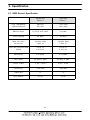
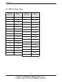
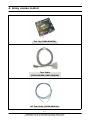
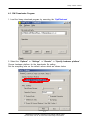
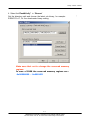
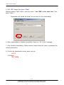
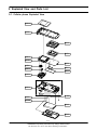
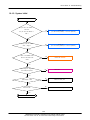
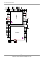
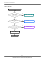
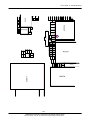
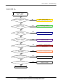
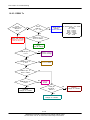
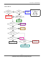
GSM TELEPHONE
SGH-B100
GSM TELEPHONE
CONTENTS
1.
Safety Precautions
2.
Specification
3.
Product Function
4.
Array course control
5.
Exploded View and Parts list
6.
MAIN Electrical Parts List
7.
Disassembly and Assembly
Instructions
8.
Block Diagrams
9.
PCB Diagrams
10. Chart of Troubleshooting
11. Reference data
GSPN (Global Service Partner Network)
Country
Web Site
North America
service.samsungportal.com
Latin America
latin.samsungportal.com
CIS
cis.samsungportal.com
Europe
europe.samsungportal.com
China
china.samsungportal.com
Asia
asia.samsungportal.com
Mideast & Africa
mea.samsungportal.com
This Service Manual is a property of Samsung Electronics Co.,Ltd.
Any unauthorized use of Manual can be punished under applicable
International and/or domestic law.
ⓒ Samsung Electronics Co.,Ltd.
2008. 01. Rev.1.0
1. Safety Precautions
1-1. Repair Precaution
● Repair in Shield Box, during detailed tuning.
Take specially care of tuning or test,
because specipicty of cellular phone is sensitive for surrounding interference(RF noise).
● Be careful to use a kind of magnetic object or tool,
because performance of parts is damaged by the influence of manetic force.
● Surely use a standard screwdriver when you disassemble this product,
otherwise screw will be worn away.
● Use a thicken twisted wire when you measure level.
A thicken twisted wire has low resistance, therefore error of measurement is few.
● Repair after separate Test Pack and Set because for short danger (for example an
overcurrent and furious flames of parts etc) when you repair board in condition of
connecting Test Pack and tuning on.
● Take specially care of soldering, because Land of PCB is small and weak in heat.
● Surely tune on/off while using AC power plug, because a repair of battery charger is
dangerous when tuning ON/OFF PBA and Connector after disassembing charger.
● Don't use as you pleases after change other material than replacement registered on SEC
System. Otherwise engineer in charge isn't charged with problem that you don't keep this
rules.
1-1
SAMSUNG Proprietary-Contents may change without notice
This Document can not be used without Samsung's authorization
Safety Precautions
1-2. ESD(Electrostatically Sensitive Devices) Precaution
Several semiconductor may be damaged easilly by static electricity. Such parts are called by
ESD(Electrostatically Sensitive Devices), for example IC,BGA chip etc. Read Precaution below.
You can prevent from ESD damage by static electricity.
● Remove static electricity remained your body before you touch semiconductor or parts with
semiconductor. There are ways that you touch an earthed place or wear static electricity
prevention string on wrist.
● Use earthed soldering steel when you connect or disconnect ESD.
● Use soldering removing tool to break static electricity. , otherwise ESD will be damaged by
static electricity.
● Don't unpack until you set up ESD on product. Because most of ESD are packed by box
and aluminum plate to have conductive power,they are prevented from static electricity.
● You must maintain electric contact between ESD and place due to be set up until ESD is
connected completely to the proper place or a circuit board.
1-2
SAMSUNG Proprietary-Contents may change without notice
This Document can not be used without Samsung's authorization
2. Specification
2-1. GSM General Specification
EG SM 9 00
Ph ase 2
DCS1 800
Phase 1
F req. Ban d[MHz]
Uplin k/Down link
8 80~915
9 25~960
1710~1 785
1805~1 880
ARF CN ra nge
0~1 24 & 9 75~102 3
512~8 85
T x/Rx spacing
45 M Hz
95 MHz
Mo d. Bit r ate/
Bit Period
270 .833 kb ps
3 . 692 u s
2 70.83 3 kbps
3.69 2 us
Ti me Slo t Pe rio d/Fr am e
Per iod
5 76.9 u s
4. 615 ms
576. 9 us
4 .615 ms
Modula tion
0 .3 G M SK
0.3 G MSK
M S Power
33 d Bm ~5 dBm
3 0 dBm ~0 dBm
Powe r Class
5 pcl ~ 19 pcl
0 pcl ~ 15 pcl
Se nsitivity
-10 2 dBm
- 100 dBm
TDMA M ux
8
8
Cell Radiu s
35 Km
2 Km
2-1
Speclflcation
2-2. GSM Tx Power Class
TX Power
control level
GSM900
TX Power
control level
DCS1800
5
33±2 dBm
0
30±3 dBm
6
31±2 dBm
1
28±3 dBm
7
29±2 dBm
2
26±3 dBm
8
27±2 dBm
3
24±3 dBm
9
25±2 dBm
4
22±3 dBm
10
23±2 dBm
5
20±3 dBm
11
21±2 dBm
6
18±3 dBm
12
19±2 dBm
7
16±3 dBm
13
17±2 dBm
8
14±3 dBm
14
15±2 dBm
9
12±4 dBm
15
13±2 dBm
10
10±4 dBm
16
11±3 dBm
9±3 dBm
11
8±4 dBm
17
18
7±3 dBm
12
6±4 dBm
19
5±3 dBm
13
4±4 dBm
14
2±5 dBm
15
0±5 dBm
2-2
3. Product Function
Main Function
- Speed dial
- Phonebook memory status
- SDN(Service Dialling Numbers)
- Network services
- Read SMS or MMS messages
- Send SMS or MMS messages
- Voicemail
- Broadcast message
- MMS profile
- SOS messages
- Web browser
- Menu shortcuts
3-1
SAMSUNG Proprietary-Contents may change without notice
This Document can not be used without Samsung's authorization
4. Array course control
Test Jig (GH80-00865A)
Test Cable
(GH39-00895A/GH39-00892A)
RF Test Cable (GH39-00397A)
4-1
SAMSUNG Proprietary-Contents may change without notice
This Document can not be used without Samsung's authorization
Array course control
Software Downloading
4-1. Downloading Binary Files
• Three binary files for downloading B100.
– B100XXYY.s3 : Main source code binary.
4-2. Pre-requsite for Downloading
• Downloader Program(OptiFlash.exe)
• B100 Mobile Phone
• Data Cable
• Binary files
4-2
SAMSUNG Proprietary-Contents may change without notice
This Document can not be used without Samsung's authorization
Array course control
4-3. S/W Downloader Program
1. Load the binary download program by executing the “OptiFlash.exe”
2. Select the “Options” -> “Settings” -> “Generic” -> “Specify hardware platform”.
Choose hardware platform for the downloader file setting.
Set the everything else as the default values which are shown below
4-3
SAMSUNG Proprietary-Contents may change without notice
This Document can not be used without Samsung's authorization
Array course control
3. Select the COM port when the download cable is connected
Up to twelve ports are supported. Additionally you can select the
maximum
transfer speed OptiFlash will use to communicate with
the phone. However, OptiFlash will use a slower speed if either the
PC’s or the phone’s serial hardware is incapable of handling the
selected speed
4-4
SAMSUNG Proprietary-Contents may change without notice
This Document can not be used without Samsung's authorization
Array course control
4. Select the“Flash&Verify” -> “Browse”
Set the directory path and choose the latest s/w binary, for example
B100XXYY.s3”, for the downloader binary setting.
Make sure that not to change the reserved memory
regions.
In case of B108 the reserved memory regions are :
-0x00008000 – 0x0001ffff
4-5
SAMSUNG Proprietary-Contents may change without notice
This Document can not be used without Samsung's authorization
“
Array course control
5. Click “OK” button then press “Flash”.
(Before pressing ‘Flash’ button, push the button ‘*’and ‘END’ at the same time. Then
press ‘Flash’.)
Downloader will upload the binary file as below for the downloading.
6. When downloading is finished successfully, there is a “All is well” message.
7. After finishing downloading, Certain memory resets should be done to guarantee the
normal performance.
8. Confirm the downloaded version name and etc. :
*#1111#
Full Reset :
*2767*3855#
4-6
SAMSUNG Proprietary-Contents may change without notice
This Document can not be used without Samsung's authorization
5. Exploded View and Parts List
5-1. Cellular phone Exploded View
QMW02
QFR01
QKP01
QME01
QMP01
QLC01
QMI01
QSP01
QSH01
QMO01
QSH02
QAN01
QRE01
QIF01
QCR68
QRF01
QCR68
QBA01
QBA00
5-1
SAMSUNG Proprietary-Contents may change without notice
This Document can not be used without Samsung's authorization
Main Electrical Parts List
5-2. Cellular phone Parts list
Design LOC
Discription
SEC CODE
QAN01
INTENNA-SGH_B108
GH42-01421A
QBA00
PMO COVER-BATTERY
GH72-45634A
QBA01
INNER BATTERY PACK-1000MAH,BLA
GH43-02424A
QCR68
SCREW-TAPPING
6002-001399
QCR68
SCREW-TAPPING
6002-001399
QFR01
ASSY CASE-FRONT
GH98-06846A
QKP01
ASSY KEYPAD-(XEF/LKA)
GH98-07043A
QLC01
LCD-LCD MODULE
GH07-01056A
QME01
DOME SHEET-22 KEY
GH59-05216A
QMI01
MICROPHONE-ASSY-SGH_B108
GH30-00447A
QMO01
MOTOR DC-SCH-S369
GH31-00392A
QMP01
PBA MAIN-SGH_B100
GH92-04320A
QMW02
PMO WINDOW-LCD
GH72-45617A
QRF01
TAPE-RF SHEET
GH74-36593A
QSH01
IPR SHIELD-COVER A
GH70-02974A
QSH02
IPR SHIELD-COVER B
GH70-02975A
QSP01
SPEAKER
3001-002289
QRE01
ASSY CASE-REAR
GH98-06845A
PMO COVER-IF
GH72-45106A
QIF01
5-2
SAMSUNG Proprietary-Contents may change without notice
This Document can not be used without Samsung's authorization
Main Electrical Parts List
Discription
SEC CODE
BAG PE
6902-000297
ADAPTOR-ATADS10EBE,BLK,EU
GH44-01702A
LABEL(P)-UNIT SEAL
GH68-00518B
LABEL(R)-WATER SOAK
GH68-09361A
MANUAL USERS-EU SPANISH
GH68-17128A
LABEL(R)-MAIN(EU)
GH68-17232A
BOX(P)-UNIT MAIN EU
GH69-06338A
SPONGE-INTENNA
GH74-35738A
SPONGE-SPK
GH74-35739A
VINYL-BOHO WINDOW A
GH74-36876A
5-3
SAMSUNG Proprietary-Contents may change without notice
This Document can not be used without Samsung's authorization
6. MAIN Electrical Parts List
SEC CODE
0401-001141
Design LOC
Discription
STATUS
D600
DIODE-SWITCHING
SA
0403-001547
ZD300
DIODE-ZENER
SA
0406-001286
ZD301
DIODE-TVS
SA
0406-001286
ZD302
DIODE-TVS
SA
0504-000168
TR300
TR-DIGITAL
SA
0601-002361
LED600
LED
SA
0601-002361
LED601
LED
SA
0601-002361
LED602
LED
SA
0601-002361
LED603
LED
SA
0601-002361
LED604
LED
SA
0601-002361
LED605
LED
SA
0801-003206
U104
IC-CMOS LOGIC
SA
1001-001349
U603
IC-ANALOG MULTIPLEX
SA
1001-001371
U401
IC-ANALOG SWITCH
SA
1108-000111
UME200
IC-MCP
SA
1201-002490
PAM100
IC-POWER AMP
SA
1203-003897
UCP300
IC-POWER SUPERVISOR
SA
1203-004640
U602
IC-DC/DC CONVERTER
SA
1203-005005
U301
IC-BATTERY
SA
1204-002783
U400
IC-SOUND GENERATOR
SA
1205-003098
U103
IC-TRANSCEIVER
SA
1205-003412
UCP200
IC-COMM. CONTROLLER
SA
1404-001165
TH200
THERMISTOR-NTC
SA
1405-001082
VR300
VARISTOR
SA
1405-001082
VR301
VARISTOR
SA
1405-001082
VR302
VARISTOR
SA
1405-001082
VR402
VARISTOR
SA
1405-001082
VR403
VARISTOR
SA
1405-001082
VR600
VARISTOR
SA
1405-001082
VR601
VARISTOR
SA
1405-001082
VR602
VARISTOR
SA
1405-001082
VR603
VARISTOR
SA
1405-001082
VR604
VARISTOR
SA
1405-001082
VR605
VARISTOR
SA
1405-001082
VR606
VARISTOR
SA
1405-001082
VR607
VARISTOR
SA
1405-001082
VR608
VARISTOR
SA
6-1
SAMSUNG Proprietary-Contents may change without notice
This Document can not be used without Samsung's authorization
Exploded View and Parts List
SEC CODE
1405-001082
Design LOC
Discription
STATUS
VR609
VARISTOR
SA
1405-001082
VR610
VARISTOR
SA
1405-001121
VR400
VARISTOR
SA
1405-001121
VR401
VARISTOR
SA
2007-000138
R304
R-CHIP
SA
2007-000138
R412
R-CHIP
SA
2007-000140
R307
R-CHIP
SA
2007-000140
R308
R-CHIP
SA
2007-000140
R309
R-CHIP
SA
2007-000140
R310
R-CHIP
SA
2007-000140
R311
R-CHIP
SA
2007-000140
R312
R-CHIP
SA
2007-000140
R313
R-CHIP
SA
2007-000141
R410
R-CHIP
SA
2007-000141
R506
R-CHIP
SA
2007-000148
R102
R-CHIP
SA
2007-000148
R316
R-CHIP
SA
2007-000148
R317
R-CHIP
SA
2007-000148
R408
R-CHIP
SA
2007-000148
R409
R-CHIP
SA
2007-000148
R502
R-CHIP
SA
2007-000148
R504
R-CHIP
SA
2007-000157
R204
R-CHIP
SA
2007-000157
R303
R-CHIP
SA
2007-000157
R419
R-CHIP
SA
2007-000160
R401
R-CHIP
SA
2007-000161
R503
R-CHIP
SA
2007-000161
R505
R-CHIP
SA
2007-000162
R203
R-CHIP
SA
2007-000162
R205
R-CHIP
SA
2007-000162
R207
R-CHIP
SA
2007-000162
R301
R-CHIP
SA
2007-000170
R107
R-CHIP
SA
2007-000170
R110
R-CHIP
SA
2007-000170
R314
R-CHIP
SA
2007-000170
R315
R-CHIP
SA
2007-000171
R100
R-CHIP
SA
6-2
SAMSUNG Proprietary-Contents may change without notice
This Document can not be used without Samsung's authorization
Exploded View and Parts List
SEC CODE
2007-000171
Design LOC
Discription
STATUS
R105
R-CHIP
SA
2007-000171
R109
R-CHIP
SA
2007-000171
R111
R-CHIP
SA
2007-000171
R420
R-CHIP
SA
2007-000171
R421
R-CHIP
SA
2007-000172
R200
R-CHIP
SA
2007-000172
R202
R-CHIP
SA
2007-000172
R402
R-CHIP
SA
2007-000172
R403
R-CHIP
SA
2007-000172
R600
R-CHIP
SA
2007-000172
R601
R-CHIP
SA
2007-000172
R602
R-CHIP
SA
2007-000172
R603
R-CHIP
SA
2007-000172
R604
R-CHIP
SA
2007-000172
R605
R-CHIP
SA
2007-000242
R407
R-CHIP
SA
2007-000242
R501
R-CHIP
SA
2007-000775
R400
R-CHIP
SA
2007-000982
R209
R-CHIP
SA
2007-001119
R405
R-CHIP
SA
2007-001119
R500
R-CHIP
SA
2007-001284
R201
R-CHIP
SA
2007-001284
R300
R-CHIP
SA
2007-001288
R417
R-CHIP
SA
2007-001288
R418
R-CHIP
SA
2007-001292
R305
R-CHIP
SA
2007-001292
R306
R-CHIP
SA
2007-001301
R103
R-CHIP
SA
2007-001307
R108
R-CHIP
SA
2007-001308
R106
R-CHIP
SA
2007-001325
R404
R-CHIP
SA
2007-001339
R302
R-CHIP
SA
2007-002797
R104
R-CHIP
SA
2007-007148
R318
R-CHIP
SA
2007-007590
R406
R-CHIP
SA
2007-007590
R411
R-CHIP
SA
2007-007741
R101
R-CHIP
SA
6-3
SAMSUNG Proprietary-Contents may change without notice
This Document can not be used without Samsung's authorization
Exploded View and Parts List
SEC CODE
2007-008403
Design LOC
Discription
STATUS
R206
R-CHIP
SA
2007-008403
R208
R-CHIP
SA
2203-000233
C220
C-CER,CHIP
SA
2203-000233
C302
C-CER,CHIP
SA
2203-000254
C203
C-CER,CHIP
SA
2203-000254
C204
C-CER,CHIP
SA
2203-000254
C208
C-CER,CHIP
SA
2203-000254
C209
C-CER,CHIP
SA
2203-000254
C210
C-CER,CHIP
SA
2203-000254
C213
C-CER,CHIP
SA
2203-000254
C215
C-CER,CHIP
SA
2203-000254
C217
C-CER,CHIP
SA
2203-000254
C300
C-CER,CHIP
SA
2203-000330
C222
C-CER,CHIP
SA
2203-000359
C401
C-CER,CHIP
SA
2203-000386
C129
C-CER,CHIP
SA
2203-000386
C221
C-CER,CHIP
SA
2203-000438
C133
C-CER,CHIP
SA
2203-000438
C324
C-CER,CHIP
SA
2203-000438
C413
C-CER,CHIP
SA
2203-000466
C115
C-CER,CHIP
SA
2203-000489
C408
C-CER,CHIP
SA
2203-000489
C411
C-CER,CHIP
SA
2203-000627
C134
C-CER,CHIP
SNA
2203-000679
C132
C-CER,CHIP
SA
2203-000679
C206
C-CER,CHIP
SA
2203-000812
C119
C-CER,CHIP
SA
2203-000812
C120
C-CER,CHIP
SA
2203-000812
C121
C-CER,CHIP
SA
2203-000812
C131
C-CER,CHIP
SA
2203-000812
C305
C-CER,CHIP
SA
2203-000812
C306
C-CER,CHIP
SA
2203-000812
C600
C-CER,CHIP
SA
2203-000812
C601
C-CER,CHIP
SA
2203-000812
C602
C-CER,CHIP
SA
2203-000812
C603
C-CER,CHIP
SA
2203-000812
C604
C-CER,CHIP
SA
6-4
SAMSUNG Proprietary-Contents may change without notice
This Document can not be used without Samsung's authorization
Exploded View and Parts List
SEC CODE
2203-000812
Design LOC
Discription
STATUS
C605
C-CER,CHIP
SA
2203-000812
C606
C-CER,CHIP
SA
2203-000812
C607
C-CER,CHIP
SA
2203-000812
C608
C-CER,CHIP
SA
2203-000812
C610
C-CER,CHIP
SA
2203-000812
C611
C-CER,CHIP
SA
2203-000812
C612
C-CER,CHIP
SA
2203-000940
C303
C-CER,CHIP
SA
2203-000995
C307
C-CER,CHIP
SA
2203-000995
C501
C-CER,CHIP
SA
2203-002709
C614
C-CER,CHIP
SA
2203-005065
C312
C-CER,CHIP
SA
2203-005065
C313
C-CER,CHIP
SA
2203-005065
C315
C-CER,CHIP
SA
2203-005065
C316
C-CER,CHIP
SA
2203-005065
C317
C-CER,CHIP
SA
2203-005234
C105
C-CER,CHIP
SA
2203-005234
L100
C-CER,CHIP
SA
2203-005344
C207
C-CER,CHIP
SA
2203-005344
C219
C-CER,CHIP
SA
2203-005344
C319
C-CER,CHIP
SA
2203-005382
C103
C-CER,CHIP
SA
2203-005482
C128
C-CER,CHIP
SA
2203-005482
C130
C-CER,CHIP
SA
2203-005482
C402
C-CER,CHIP
SA
2203-005683
C108
C-CER,CHIP
SA
2203-005683
C110
C-CER,CHIP
SA
2203-005719
C101
C-CER,CHIP
SA
2203-005719
C106
C-CER,CHIP
SA
2203-005719
C107
C-CER,CHIP
SA
2203-005719
C117
C-CER,CHIP
SA
2203-005719
C124
C-CER,CHIP
SA
2203-005736
C111
C-CER,CHIP
SA
2203-005736
C118
C-CER,CHIP
SA
2203-005736
C125
C-CER,CHIP
SA
2203-005777
C114
C-CER,CHIP
SA
2203-005819
C321
C-CER,CHIP
SA
6-5
SAMSUNG Proprietary-Contents may change without notice
This Document can not be used without Samsung's authorization
Exploded View and Parts List
SEC CODE
2203-005819
Design LOC
Discription
STATUS
C619
C-CER,CHIP
SA
2203-005819
C621
C-CER,CHIP
SA
2203-005819
C622
C-CER,CHIP
SA
2203-006048
C200
C-CER,CHIP
SA
2203-006048
C201
C-CER,CHIP
SA
2203-006048
C202
C-CER,CHIP
SA
2203-006048
C205
C-CER,CHIP
SA
2203-006048
C211
C-CER,CHIP
SA
2203-006048
C212
C-CER,CHIP
SA
2203-006048
C214
C-CER,CHIP
SA
2203-006048
C216
C-CER,CHIP
SA
2203-006048
C218
C-CER,CHIP
SA
2203-006048
C301
C-CER,CHIP
SA
2203-006048
C311
C-CER,CHIP
SA
2203-006048
C314
C-CER,CHIP
SA
2203-006048
C318
C-CER,CHIP
SA
2203-006048
C320
C-CER,CHIP
SA
2203-006048
C323
C-CER,CHIP
SA
2203-006048
C405
C-CER,CHIP
SA
2203-006048
C407
C-CER,CHIP
SA
2203-006048
C409
C-CER,CHIP
SA
2203-006048
C410
C-CER,CHIP
SA
2203-006048
C414
C-CER,CHIP
SA
2203-006048
C417
C-CER,CHIP
SA
2203-006048
C418
C-CER,CHIP
SA
2203-006048
C500
C-CER,CHIP
SA
2203-006048
C502
C-CER,CHIP
SA
2203-006137
C326
C-CER,CHIP
SA
2203-006137
C400
C-CER,CHIP
SA
2203-006194
C104
C-CER,CHIP
SA
2203-006194
C112
C-CER,CHIP
SA
2203-006257
C304
C-CER,CHIP
SA
2203-006257
C309
C-CER,CHIP
SA
2203-006257
C403
C-CER,CHIP
SA
2203-006260
C127
C-CER,CHIP
SA
2203-006324
C308
C-CER,CHIP
SA
2203-006348
C322
C-CER,CHIP
SA
6-6
SAMSUNG Proprietary-Contents may change without notice
This Document can not be used without Samsung's authorization
Exploded View and Parts List
SEC CODE
2203-006361
Design LOC
Discription
STATUS
C613
C-CER,CHIP
SA
2203-006423
C100
C-CER,CHIP
SA
2203-006423
C122
C-CER,CHIP
SA
2203-006423
C123
C-CER,CHIP
SA
2203-006462
C126
C-CER,CHIP
SA
2203-006556
C116
C-CER,CHIP
SA
2203-006562
C412
C-CER,CHIP
SA
2203-006562
C415
C-CER,CHIP
SA
2203-006562
C421
C-CER,CHIP
SA
2203-006626
C113
C-CER,CHIP
SA
2203-006824
C325
C-CER,CHIP
SA
2203-006824
C404
C-CER,CHIP
SA
2203-006839
C109
C-CER,CHIP
SA
2203-006841
C327
C-CER,CHIP
SA
2203-006872
C406
C-CER,CHIP
SA
2203-006872
C416
C-CER,CHIP
SA
2404-001336
TA400
C-TA,CHIP
SA
2404-001336
TA500
C-TA,CHIP
SA
2404-001406
TA300
C-TA,CHIP
SA
2404-001415
TA100
C-TA,CHIP
SA
2404-001415
TA600
C-TA,CHIP
SA
2703-001236
L106
INDUCTOR-SMD
SA
2703-001722
L103
INDUCTOR-SMD
SA
2703-001723
L603
INDUCTOR-SMD
SA
2703-001723
L604
INDUCTOR-SMD
SA
2703-001723
L605
INDUCTOR-SMD
SA
2703-001723
L606
INDUCTOR-SMD
SA
2703-001737
L101
INDUCTOR-SMD
SA
2703-001737
L107
INDUCTOR-SMD
SA
2703-001747
L104
INDUCTOR-SMD
SA
2703-001990
L108
INDUCTOR-SMD
SA
2703-002200
L400
INDUCTOR-SMD
SA
2703-002200
L401
INDUCTOR-SMD
SA
2703-002484
L102
INDUCTOR-SMD
SA
2801-003856
OSC200
CRYSTAL-SMD
SA
2801-004689
OSC100
CRYSTAL-SMD
SA
2904-001792
F100
FILTER-SAW
SA
6-7
SAMSUNG Proprietary-Contents may change without notice
This Document can not be used without Samsung's authorization
Exploded View and Parts List
SEC CODE
3301-001534
Design LOC
Discription
STATUS
L105
BEAD-SMD
SA
3301-001729
L600
BEAD-SMD
SA
3705-001358
RFS100
CONNECTOR-COAXIAL
SA
3709-001355
SIM300
CONNECTOR-CARD EDGE
SA
3710-002499
IFC300
SOCKET-INTERFACE
SA
3711-006084
BTC300
HEADER-BATTERY
SA
GH70-02367A
SC100
ICT-ON-BOARD CLIP
SA
GH70-02367A
SC104
ICT-ON-BOARD CLIP
SA
GH70-02640A
SC101
ICT SHIELD-CAN CLIP
SA
GH70-02640A
SC102
ICT SHIELD-CAN CLIP
SA
GH70-02640A
SC103
ICT SHIELD-CAN CLIP
SA
GH70-02640A
SC105
ICT SHIELD-CAN CLIP
SA
GH71-07891A
U604
NPR SHIELD-FRAME A
SA
Please consult the GSPN website (Samsung Portal) for the most recent version of the product's
part list.
6-8
SAMSUNG Proprietary-Contents may change without notice
This Document can not be used without Samsung's authorization
7. Disassembly and Assembly Instructions
7-1. Disassembly
1
2
1) Release SCREW 4 POINT at Rear
※ caution
1) Be careful not to make scratch and molding
damage!
1) Disjoint HOOK from down to up.
※ caution
1) Be careful not to make scratch and molding
damage!
3
4
Braket's
HOOK
Braket's
HOOK
1) Disjoint the Low Braket's HOOK (3 point)
※ caution
1) Be careful not to make scratch and molding
damage!
1) Disjoint the HIGH Braket's HOOK (2 point)
※ caution
1) Be careful not to make scratch and molding
damage!
7-1
SAMSUNG Proprietary-Contents may change without notice
This Document can not be used without Samsung's authorization
Exploded View and Parts List
5
1 Sperate Braket from the main PBA.
※ caution
1) Be careful not to make scratch and molding
damage!
2) Beware that you do not damage MIC F-PCB.
7-2
SAMSUNG Proprietary-Contents may change without notice
This Document can not be used without Samsung's authorization
Exploded View and Parts List
7-2. Assembly
2
1
1) Set a PBA on the FRONT.
※ caution
1) Put the PBA on the FRONT.
※ caution
1) Be careful not to make scratch and molding
1) Be careful not to make scratch and molding
damage!
damage!
3
4
Braket's
HOOK
1) Assemble the FRONT's hook 3point.
※ caution
1) Be careful not to make scratch and molding
1) Put the MIC on the FRONT.
※ caution
1) Be careful not to make scratch and molding
damage!
damage!
2) Beware that you do not damage MIC F-PCB.
2) Beware that you do not damage MIC F-PCB.
7-3
SAMSUNG Proprietary-Contents may change without notice
This Document can not be used without Samsung's authorization
Exploded View and Parts List
6
5
1) Assemble REAR and FRONT ass'y.
※ caution
1) Be careful not to make scratch and molding
1) Assemble the FRONT's hook
※ caution
1) Be careful not to make scratch and molding
damage!
damage!
7
1) Drivers 4 screws on the REAR.
※ caution
1) Be careful not to make scratch and molding
damage!
7-4
SAMSUNG Proprietary-Contents may change without notice
This Document can not be used without Samsung's authorization
8. Block Diagrams
8-1
SAMSUNG Proprietary-Contents may change without notice
This Document can not be used without Samsung's authorization
R4 0 3
C4 1 0
R4 0 1
R4 1 8
R4 1 9
R4 0 2
C4 0 9
C4 2 1
R4 1 2
C3 1 8
TR3 0 0
C300
R1 0 6
C204
R108
C219
C206
R202
R105
R1 0 4
C1 2 9
C207
C320
GND600
R1 1 0
U301
F100
C1 3 3
C1 3 1
C1 3 0
R314
C2 1 2
C201
C2 1 4
C2 1 8
R2 0 8
C2 0 5
R2 0 6
R2 0 4
C602
C603
C601
SI M 3 0 0
SC100
L1 0 5
C1 2 8
C200
C606
C607
C604
C605
C600
C2 0 8
R203
R207
R3 1 5
C215
TH200
U1 0 4
C220
UCP200
C3 1 9
R1 0 9
C4 0 5
C1 1 7
C1 1 0
C1 0 8
C4 1 4
C4 1 3
C3 1 4
C3 0 9
R5 0 5
R5 0 4
C5 0 2
C5 0 0
R5 0 2
R5 0 3
C417
C1 2 4
C1 0 7
L1 0 6
C211
R205
R201
R1 0 7
C221
SC1 0 1
R5 0 0
U6 0 3
TA 6 0 0
U4 0 1
CN3 0 0
R3 0 2
C4 0 8
C4 1 1
C4 1 2
C4 1 6
C418
R408
C4 1 5
R4 0 4
R409
U1 0 3
C1 2 7
C3 0 3
R3 0 0
C3 0 4
C3 0 5
C3 0 6
C3 0 7
R420
R411
C1 1 3
C301
C202
UME200
OSC200
C222
R417
C4 0 1
C1 2 0
C1 2 1
R1 0 2
C1 1 9
C12 5
C1 2 6
VR402
C3 2 6
R3 0 4
C6 2 2
R400
C1 1 5
R407
TA400
R405
R310
C3 2 2
R3 1 6
R3 1 8
C6 1 9
L1 0 1
L1 0 8
L1 0 4
UCP3 0 0
ZD30 1
L4 0 1
L4 0 0
C3 2 5
C6 0 8
C6 1 1
C403
R1 0 3
C209
C216
C217
R209
C203
R311
C6 1 0
RFS1 0 0
R4 1 0
R4 2 1
VR4 0 3
9-1
C210
R200
C213
R101
R306
ZD302
R1 0 0
U6 0 2
L6 0 4
D6 0 0
C6 1 3
C3 1 1
V R3 0 0
OSC100
L1 0 0
C308
C132
C312
C134
C106
C315
C101
R305
R1 1 1
C400
PWR_KEEP
C313
C316
C123
R313
C323
R406
L102
L103
C321
C122
C111
C118
VR301
C1 3 5
C302
C112
C407
TA100
R308
R303
GND
C100
C406
C109
R506
C501
C621
R312
C612
L603
L606
TA500
L107
C105
C327
R317
C324
R309
L600
VR40 0 VR401
R307
R301
R501
C103
VR302
BTC300
L605
C614
ZD300
TA300
U400
C114
C317
C104
S C1 0 2
TP100
TP101
C404
PAM1 0 0
9. PCB Diagrams
KEY600
MOTOR1
SC103
C116
C402
R6 0 2
LED 6 0 2
R6 0 4
R6 0 1
TP_D(1)
LED 6 0 1
TP_ W E
CP_ T D O
CLEAR
V R6 0 0
TP_OE
TP_ CSRATM
P_ CSRO M
DOWN
CP_TMS
V R6 0 3 V R6 0 4 V R6 0 5 VR6 0 1
R6 0 3
LED 6 0 3
LED 6 0 5
R6 0 5
9-2
RI GH T
VR606
V R6 0 7
VR608
STO
MENU
SHARP
0
*
9
8
7
6
5
4
3
2
1
VR602
INTRQ
PW R
VR609
SEND
UP
V R6 1 0
LED600
I
LEFT
LED604
R6 0 0
CP_TDICP_TCK
TP_ 1 . 8 V
PCB Diagrams
U600
DSP_IO
TP_A(1)
RST
10. Flow Chart of Troubleshooting
10-1.Baseband
10-1-1. Power ON
'Power On' does not work
Check the current consumption
Yes
Current consumption
>= 100mA
No
Download again
Yes
Check the Vbat Voltage
Voltage >=3.3V
No
Charge the Battery
Yes
Check the pin of UCP300
Pin#J12 >= 2.8V
No
Check UCP300 and C316
Yes
Pin#A13 and
pin#A14 =2.8V
No
pin#G11 =
1.8V
Yes
No
Check UCP300 and C317
Yes
Check the clock signal at pin#21 of U103
Freq = 26MHz
Vpp >=400mV
Vpp≒ 600mV
No
Check the clock generation circuit
(related to OSC100)
Yes
Check the clock signal at pin#5,#6 of U104
Freq = 13MHz
No
Check U104
Yes
Check the initial operation
END
10-1
SAMSUNG Proprietary-Contents may change without notice
This Document can not be used without Samsung's authorization
Flow Chart of Troubleshooting
409
402
419
421
412
408
411
412
416
404
414
R5 0 2
R5 0 3
C5 0 0
C5 0 2
R5 0 4
C3 0 9
R5 0 5
C3 1 4
C4 1 3
C3 1 8
C3 1 9
C1 0 8
C1 1 7
C1 1 0
C122
C1 2 4
U1 0 3
C1 1 3
C112
L102
415
109
405
C1 2 6
L103
R411
R409
C418
R406
R408
C417
C302
C123
C313
C1 2 7
C308
C321
C316
C315
C317
R101
GND
C213
C312
C132
SC1 0 2
TR3 0 0
C301
C300
C320
GND600
R200
C210
C203
C216
C217
R205
C220
R209
R201
C215
C211
C219
C206
R202
R105
C207
UCP200
C209
VRF_2.9V
L105
VCCD_2.9V
VCCA_2.9V
C128
9
C302
8
NC
VBAT
C300
VCC
1 _SD
C301
2
CP 7
_RD
D
R107
1
3 Q
L106
U104
VSIM
VRTC
LED2_DRV
LED1_DRV
RING_DRV
VIB_DRV
VLDO_7
VLDO_6
VL5S_B
VL5S_A
VLDO_5
VL4S_B
VL4S_A
VLDO_4
VLDO_3
VLDO_2
VLDO_1
VACC
K12
H11
G12
G13
F13
F15
C12
A14
C9
D10
B10
B11
A12
B12
A13
J12
G11
F14
VSIM
KEY_BL1
VRF_2.9V
OSC100
C309
GND1 HOT
2
BAND_SEL
C104
C107
L104
KEY_COL(2)
C126
C122
C123
27
26
25
24
23
Q
28
29
I
C127
SERLE
SERCLK
SERDAT
RTXIN
RTXIP
10-2
SAMSUNG Proprietary-Contents may change without notice
This Document can not be used without Samsung's authorization
GND
DCS_LNA_IN_P
DCS_LNA_IN_N
GSM_LNA_IN_P
32
31 30
GSM_LNA_IN_N
33
VCC_FE
RX850
2
VLDO3
RX850B
TR300
KEY_ROW(0)
VCC_BB Q
21
20
19
22
QB
REFIN
REFINB
VA FC
TXOP_LO
8
2
RX900
TXOP_HI
1
12
C116
11
R103
RX900B
VCC_TXVCO
NC
C115
RX1800
U103
NC
35
NC
34
GSM_PAM_IN
VIB_EN
INTRQ
PWR_KEEP
RST
C114
RX1900
RX1800B
VDD
10
DPCS_PAM_IN
RX1900B
VBAT
3
13
RTCALARM
VLDO2
VLDO1
C113
14
C112
IB
15
16
VCC_REF
VBAT
REF_OP
17
VCCD_2.9V
9
N4 RTC_CL K
D1 XOENAQ
R6 MC
P5 NC7
P3 DINTR
RTXQP
R101
C106
SDATA
C318
VCC_B B I
C317
SCLK
C316
5
C315
6
C314
4
C313
VREF
PWR_SW2
PWR_SW1N
PSW1_BUF
RESET_O
RSVD2
PWR_K EEP
INTRQ
RSVD
J IG_ON
PWR_ON
CL K 32K
DSP_INT
CL K 13M_MC
RTXQN
AFC
C312
18
UP_CS
UP_SCLK
UP_SDO VBAT
UP_SDI
C319
3
1
26M_OUT
C14
C15
L7
K9
N10
M9
L10
L9
A OUTAP
A OUTAN
A OUTBP
A OUTBN
MICINP
MICINN
MICOUTP
MICOUTN
A UXINP
A UXINN
A UXOUTP
A UXOUTN
VXVCM
VREGP
VREGN
DAICK
DAIRN
DAIDI
DAIDO
P11
N12
R12
P12
N14
M14
N15
P15
M15
L14
K1 3
L13
R13
M13
R14
R4
P4
L6
M6
RTXIP
RTXIN
RTXQP
RTXQN
A OUTA P
A OUTA N
A OUTB P
A OUTB N
MICINP
MICINN
MICOUTP
MICOUTN
A UXINP
A UXINN
A UXOUTP
A UXOUTN
3
4
HOT GND2
C100
C101
NC3 D15
NC9 E10
VREF A10
CREF E9
RTC_ALMN H10
1
4
VCCD_2.9V
VRF_2.9V
VCCD_1.8V
VIB_DRV
INTRQ
PWR_KEEP
C321
R108
VRTC_3V
VCCB_2.9V VCCA_2.9V
VEXT E14
VBAT E13
CH_BDRV E11
CH_ISEN F12
CH_RES D14
C320
R105
5
R110
B4
C4
P13
L11
F6
A6
M10
N11
P6
R2
K4
G5
J4
N5
N6
M3
J3
F11
K15
B15
E8
B13
C10
SIMCLK
SIMRST
SIMDATA
SIM_IO
SIM_RST
SIM_CLK
SEN
SERLE1
SERLE2
SERDA
SERCK
N9
R10
P10
J11
K11
K14
7
B1
A2
C1
C2
R104
C129
6
VDD34 C11
VDD12 J13
UP_CLK
UP_RST
UP_IO
SIM_IO
SIM_RST
SIM_CLK
CSN_PSC K8
SCLK_PSC L8
SDO_PSC N7
SDI_PSC M7
RAREF2
RAREF1
RXTXIP
RXTXIN
RXTXQP
RXTXQN
TX_EN
SERLE
SERDAT
SERCLK
NC4
OCTL1
OCTL2
NC
OCTL4
OCTL5
OCTL6
OCTL7
D9 A FC
E7 TXP
VMOD_EN
E6
C5
F5
E5
A4
G6
B3
A3
UCP300
G-CSP2100B1-YV10
B5
B6
D7
D6
C7
C6
DSP_IO
DSP_RWN
FLASH_RESET
A FC
VA PC
DSP_AB(0:8)
C134
GND_OCTL
VDD_OCTL
GNDV
VDDV
GNDB
VDDB
GNDD
VDDD
VSS4
VSS3
VSS2
VSS1
VDD_IO2
VDD_IO1
VDD3
VDD2
VDD1
GND_HCUR
GND_PSC2
GND_PSC1
GNDQ
VDD67
VDD5
NC6
NC5
GNDS17
GNDS16
GNDS15
GNDS14
GNDS13
GNDS12
GNDS11
GNDS10
GNDS9
GNDS8
GNDS7
GNDS6
GNDS5
GNDS4
GNDS3
GNDS2
GNDS1
NC8
2
1
K10
J 10
J9
J8
J7
H9
H8
H7
H6
G10
G9
G8
G7
F10
F9
F8
F7
D13
C308
DB15
DB14
DB13
DB12
DB11
DB10
DB9
DB8
DB7
DB6
DB5
DB4
DB3
DB2
DB1
DB0
AB8
AB7
AB6
AB5
AB4
AB3
AB2
AB1
AB0
I|O
RWN
RESETN_CSP
_Q
GND
C131
C130
C133
26M_OUT
DSP_DB(0:15)
D2
D3
E3
E2
F3
F2
F1
F4
G4
G3
H5
J6
J5
K3
K2
K1
K5
K7
M1
M2
N2
N1
L5
P1
K6
DSP_IO L3
L2
R3
C2 0 8
R108
R3 1 5
C204
C1 2 9
U1 0 4
C1 3 0
C1 3 1
R203
R207
R1 0 4
R1 1 0
C1 3 3
R1 0 7
C1 2 8
L1 0 5
TH200
VCCD_2.9V
DSP_DB(15)
DSP_DB(14)
DSP_DB(13)
DSP_DB(12)
DSP_DB(11)
DSP_DB(10)
DSP_DB(9)
DSP_DB(8)
DSP_DB(7)
DSP_DB(6)
DSP_DB(5)
DSP_DB(4)
DSP_DB(3)
DSP_DB(2)
DSP_DB(1)
DSP_DB(0)
DSP_AB(8)
DSP_AB(7)
DSP_AB(6)
DSP_AB(5)
DSP_AB(4)
DSP_AB(3)
DSP_AB(2)
DSP_AB(1)
DSP_AB(0)
R1 0 6
C134
C106
PWR_KEEP
UCP3 0 0
OSC100
C104
C1 0 7
C100
L1 0 6
C101
R106
C132
R109
CLK13M_TR
CLK13M_MC
CLK13M_MXIC
Flow Chart of Troubleshooting
10-1-2. System Initial
Initial Failure
Yes
The pin #G11 of UCP300 =
1.8V and
No
Check the UCP300
(if it has some problem, it is to be replaced.)
No
Check the UCP300
(if it has some problem, it is to be replaced.)
the pin #J12 of UCP300 =
2.8V ?
Yes
Is the pin #K9 of UCP300
"Low → High" ?
Yes
There is 32.768kHz wave
No
forms at the C221 and
Check the UCP200
C222
Yes
The voltage is "High" at
No
the C316,C317,C318
Check the UCP300
Yes
LCD display is O.K
No
Check the LCD part
Yes
Sound is O.K
No
Check the Audio part
Yes
END
10-3
SAMSUNG Proprietary-Contents may change without notice
This Document can not be used without Samsung's authorization
Flow Chart of Troubleshooting
9
2
9
1
2
8
1
2
6
4
4
5
R5 0 3
R5 0 2
C5 0 0
C5 0 2
R5 0 4
R5 0 5
C3 0 9
C3 1 4
C4 1 3
C3 1 8
C3 1 9
R411
R409
C418
R406
R408
C417
C302
C321
C313
C316
UCP3 0 0
C308
C315
C317
C317
PWR_KEEP
GND
C312
R1 0 6
C213
C132
C300
SC1 0 1
TR3 0 0
R6 0 6
C301
C320
GND600
C203
C216
C211
C217
R205
C220
R209
R201
C215
TH200
R203
R207
C204
C219
C206
R202
C1 2 9
C209
UCP200
R3 1 5
C2 0 8
C210
R1 0 4
R200
C207
C2 1 2
C2 1 4
R314
C201
R2 0 8
C2 1 8
R2 0 6
C2 0 5
R2 0 4
C222
OSC200
C221
10-4
SAMSUNG Proprietary-Contents may change without notice
This Document can not be used without Samsung's authorization
Flow Chart of Troubleshooting
VCCD_2.9V
VCCD_1.8V
VCCD_1.8V VCCD_2.9V
VRTC_3V
VCCD_1.8V
R201
C206
C207
VREF
CLK13M_TR
TR_RST
E15
G15
L12
K11
N4
R12
U5
DSP_AB(8)
DSP_AB(7)
DSP_AB(6)
DSP_AB(5)
DSP_AB(4)
DSP_AB(3)
DSP_AB(2)
DSP_AB(1)
DSP_AB(0)
P10
R11
T11
U11
M8
N8
N7
P7
M6
R7
T7
U7
P6
R6
U6
P5
DSP_DB(15)
DSP_DB(14)
DSP_DB(13)
DSP_DB(12)
DSP_DB(11)
DSP_DB(10)
DSP_DB(9)
DSP_DB(8)
DSP_DB(7)
DSP_DB(6)
DSP_DB(5)
DSP_DB(4)
DSP_DB(3)
DSP_DB(2)
DSP_DB(1)
DSP_DB(0)
DSP_INT
DSP_IO
DSP_RWN
DSP_AB(8:0)
DSP_DB(15:0)
VBAT
R206
D12
R205
TH200
ICHRG
NTCCM10054BH103HC
R207
B7
XBSWN
A7
X1RTC
D10
X2RTC
E8
XRTCALARM_N
C6
XOSC32OUT
C218
R208
OSC200
C221
C217
R209
3
C222
2
KEY_COL(0:4)
TR_RST
RTCALARM
CLK32K
CP_TDO
TR_RST
CP_TDI
CP_TMS
CP_TCK
DEBUG_DSR
EAR_SWITCH
AS1
JACK_IN
PWR_KEEP
SIMRST
KEY_COL(0)
KEY_COL(1)
KEY_COL(2)
KEY_COL(3)
KEY_COL(4)
KEY_ROW(0:4)
VCCB_2.9V
M12
D7
XCP_TCK
G8
XCP_TMS
C7
XCP_TDI
F9
XCP_TRSTN
D13
XCP_TDO
E4
P13 PN17/DRQ
N17 PA18/T_ACK
M17 PA33/T_REQA
PA34/T_REQB
G6
G3 PA13/TX1
PA14/RX1
G5
F1 PA28/IOM0
PA29/IOM1
R203
T17
T14
R14
P12
P11
N11
R13
M10
U13
D11
XAG3
E11
XAG2
A11
XAG1
B11
XAG0
F3
E1 PA30/IM0
PA31/IM1
L4
C220
TR_RST
4
XCPTSTSTOP_CKO
H4
XPA 15/TX0
L3
XPA 16/RX0
MXIC_IRQ
G16
F10
E10
C11
D8
F17
C12
XTIC_MODE
M9 XPA7/IRQ1
T5
XPA8/IRQ2
P2
XPA9/IRQ3
N2
XPA10/IRQ4
INTRQ
VSS_DPL L
VDD_DPL L
XVREF
VSSA
VDDA
VRTC
CK I
RSTB
XCP_CSROMEN
XCP_CSRAMEN
XPA0/CS1N
XPA1/CS2N
XPA2/CS3N
XPA3/CS4N
K5
XPA 11/IRDA RX
N1
XPA 12/IRDA TX
UPPER_BYTE
B 14
E17
E16
N16
U16
U15
P8
U2
M1
B1
DB#15
DB#14
DB#13
DB#12
DB#11
DB#10
DB#9
DB#8
DB#7
DB#6
DB#5
DB#4
DB#3
DB#2
DB#1
DB#0
C13
XCP_WEN
P16
XPA4/OEN
P15
XPA5/WAITN
T15 XPA6/BE1N
CP_WEN
CP_OEN
VDDE
VDDE
VDDE
VDDE
VDDE
VDDE
VDDE
VDDE
VDDE
VDDE
C16
A5
R17
R16
T13
R4
R1
G1
E2
VDD
VDD
VDD
VDD
VDD
VDD
VDD
VDD
VDD
L9
J 11
L8
M7
L 10
L6
K7
K6
J7
H11
H7
G10
G9
F6
A3
A2
UCP200
M3
G2 PA25/OM0
G4 PA26/OM1
PA27/SM1_CL K
A12
A13
M15
M14
M11
N14
CP_CSROMEN
CP_CSRAMEN
TORCH_EN
LCD_CS
EAR_CHECK
YMU_EN
XCP_A0_BEON
XCP_A1
XCP_A2
XCP_A3
XCP_A4
XCP_A5
XCP_A6
XCP_A7
XCP_A8
XCP_A9
XCP_A10
XCP_A11
XCP_A12
XCP_A13
XCP_A14
XCP_A15
XCP_A16
XCP_A17
XCP_A18
XCP_A19
XCP_A20
XCP_A21
AB#8
AB#7
AB#6
AB#5
AB#4
AB#3
AB#2
AB#1
AB#0
R5
XPWM1
H6
XPA 23/PWM2
H5
XPA 24/PWM3
F4
FL A SH_RESET
A(21)
CKO/IACK/ERAMHI
IOBIT[2]/VEC[3]/EROMHI
IOBIT[1]/VEC[4]/PLLTOA
INT#0
IO7
RWN
L2
L 1 PA19/CP_MO
K 4 PA20/CP_MI
XPA 21/CP_SCK
J6
PA22/SM1_DA TA
B13
F11
E14
D15
B15
C14
A16
A15
B17
C17
D16
F14
G14
G13
G17
J12
K12
K13
K14
L14
L15
L16
F12
TDO
F15
TRST
H12
TDI
G12
TMS
H13
TCK
U12
N10 SIM_DA TA /SM0_DAT A
SIM_CL K /SM0_CL K
A(0)
A(1)
A(2)
A(3)
A(4)
A(5)
A(6)
A(7)
A(8)
A(9)
A(10)
A(11)
A(12)
A(13)
A(14)
A(15)
A(16)
A(17)
A(18)
A(19)
A(20)
XCP_D0
XCP_D1
XCP_D2
XCP_D3
XCP_D4
XCP_D5
XCP_D6
XCP_D7
XCP_D8
XCP_D9
XCP_D10
XCP_D11
XCP_D12
XCP_D13
XCP_D14
XCP_D15
CP_K B [ 0] /TR_CS_IRA M
CP_K B [ 1] /TR_CS_IROM
CP_K B [ 2] /TR_CS_PERF
CP_K B [ 3]/TR_CS_IPCP
CP_K B [ 4]/TR_SIZE0
CP_K B [ 5]/TR_CL K
CP_K B [ 6] /TR_PROT0
CP_K B [ 7] /TR_SI ZE1
CP_K B [ 8] /TR_NEXEC
CP_K B [ 9] /TR_GNT_DMA
R204
A6
B5
F8
F7
C5
D6
E7
D5
C4
B4
B3
C1
C2
D2
D3
E3
L5
M4
T1
R2
T3
U3
P3
T4
N3
A(0:20)
D(0)
D(1)
D(2)
D(3)
D(4)
D(5)
D(6)
D(7)
D(8)
D(9)
D(10)
D(11)
D(12)
D(13)
D(14)
D(15)
VSS
VSS
VSS
VSS
VSS
VSS
VSS
VSS
VSS
VSS
VSS
VSS
VSS
VSS
VSS
VSS
1
NC
2
NC
N15
XPA 36_A 23_CS5N
L 13
XPA 35_A 22
L 17
VDD
H14
XPA 32_CS0N
TP_1.8V
D(0:15)
KEY_ROW(0)
KEY_ROW(1)
KEY_ROW(2)
KEY_ROW(3)
KEY_ROW(4)
DEBUG_DTR
DEBUG_RTS
DEBUG_TXD
DEBUG_RXD
DEBUG_CTS
CHG_DET
SDS_TXD
SDS_RXD
SIMDATA
SIMCLK
FLASH_RESET
LED_EN
CHG_OFF
UP_CS
UP_SCLK
UP_SDO
UP_SDI
VCCD_2.9V
VCCD_2.9V
VCCA_2.9V
VBAT
C300
C302
C301
DSP_DB(0:15)
B1
A2
C1
C2
SERLE1
SERLE2
SERDA
SERCK
B4
C4
P13
L 11
F6
A6
M10
N11
P6
R2
K4
G5
J4
N5
N6
M3
J3
F11
K 15
B 15
E8
B 13
C10
VDD34 C11
VDD12 J13
UP_CLK
UP_RST
UP_IO
SIM_IO
SIM_RST
SIM_CLK
N9
R10
P10
J11
K11
K14
SIMCLK
SIMRST
SIMDATA
SIM_IO
SIM_RST
SIM_CLK
VSIM
VRTC
LED2_DRV
LED1_DRV
RING_DRV
VIB_DRV
VLDO_7
VLDO_6
VL5S_B
VL5S_A
VLDO_5
VL4S_B
VL4S_A
VLDO_4
VLDO_3
VLDO_2
VLDO_1
VACC
K12
H11
G12
G13
F13
F15
C12
A14
C9
D10
B10
B11
A12
B12
A13
J12
G11
F14
VSIM
KEY_BL1
VRTC_3V
VCCB_2.9V VCCA_2.9V
VCCD_2.9V
VRF_2.9V
VCCD_1.8V
VIB_DRV
C309
BAND_SEL
CSN_PSC K8
SCLK_PSC L8
SDO_PSC N7
SDI_PSC M7
UP_CS
UP_SCLK
UP_SDO VBAT
UP_SDI
C312
C313
C314
C315
C316
C317
VREF
PWR_SW2
PWR_SW1N
PSW1_B UF
RESET_O
RSVD2
PWR_KEEP
INT RQ
RSVD
RTC_CL K
XOENA Q
MC
NC7
DINTR
N4
D1
R6
P5
P3
NC3 D15
NC9 E10
VREF A10
CREF E9
RTC_ALMN H10
RTCALARM
C319
C14
C15
L7
K9
N10
M9
L 10
L9
AOUTA P
AOUTA N
AOUTB P
AOUTB N
MICINP
MICINN
MICOUTP
MICOUTN
AUXINP
AUXINN
AUXOUTP
AUXOUTN
VXVCM
VREGP
VREGN
DA ICK
DA IRN
DA IDI
DA IDO
P11
N12
R12
P12
N14
M14
N15
P15
M15
L 14
K 13
L 13
R13
M13
R14
R4
P4
L6
M6
VEXT E14
VBAT E13
CH_BDRV E11
CH_ISEN F12
CH_RES D14
JIG_ON
PWR_ON
DSP_INT
CL K 13M_MC
C320
C321
CL K32K
INTRQ
PWR_KEEP
AOUTA P
AOUTAN
AOUTB P
AOUTBN
MICINP
MICINN
MICOUTP
MICOUTN
A UXINP
AUXINN
A UXOUTP
A UXOUTN
TX_EN
SERLE
SERDAT
SERCLK
NC4
OCTL1
OCTL2
NC
OCTL4
OCTL5
OCTL6
OCTL7
RTXIP
RTXIN
RTXQP
RTXQN
VMOD_EN
E6
C5
F5
E5
A4
G6
B3
A3
UCP300
RA REF2
RA REF1
RXTXIP
RXTXIN
RXTXQP
RXTXQN
DSP_IO
DSP_RWN
FLASH_RESET
DB15
DB14
DB13
DB12
DB11
DB10
DB9
DB8
DB7
DB6
DB5
DB4
DB3
DB2
DB1
DB0
AB8
AB7
AB6
AB5
AB4
AB3
AB2
AB1
AB0
I|O
RWN
RESETN_CSP
D9 AFC
E7 TXP
DSP_AB(0:8)
D2
D3
E3
E2
F3
F2
F1
F4
G4
G3
H5
J6
J5
K3
K2
K1
K5
K7
M1
M2
N2
N1
L5
P1
K6
DSP_IO L3
L2
R3
B5
B6
D7
D6
C7
C6
DSP_DB(15)
DSP_DB(14)
DSP_DB(13)
DSP_DB(12)
DSP_DB(11)
DSP_DB(10)
DSP_DB(9)
DSP_DB(8)
DSP_DB(7)
DSP_DB(6)
DSP_DB(5)
DSP_DB(4)
DSP_DB(3)
DSP_DB(2)
DSP_DB(1)
DSP_DB(0)
DSP_AB(8)
DSP_AB(7)
DSP_AB(6)
DSP_AB(5)
DSP_AB(4)
DSP_AB(3)
DSP_AB(2)
DSP_AB(1)
DSP_AB(0)
GND_OCTL
VDD_OCTL
GNDV
VDDV
GNDB
VDDB
GNDD
VDDD
VSS4
VSS3
VSS2
VSS1
VDD_IO2
VDD_IO1
VDD3
VDD2
VDD1
GND_HCUR
GND_PSC2
GND_PSC1
GNDQ
VDD67
VDD5
NC6
NC5
GNDS17
GNDS16
GNDS15
GNDS14
GNDS13
GNDS12
GNDS11
GNDS10
GNDS9
GNDS8
GNDS7
GNDS6
GNDS5
GNDS4
GNDS3
GNDS2
GNDS1
NC8
2
1
K 10
J 10
J9
J8
J7
H9
H8
H7
H6
G10
G9
G8
G7
F10
F9
F8
F7
D13
C308
AFC
VAPC
BP_CF
C205
1
A(22)
A(23)
C204
1
3
2
VIB_EN
INTRQ
PWR_KEEP
RST
KEY_COL(2)
TR300
KEY_ROW(0)
10-5
SAMSUNG Proprietary-Contents may change without notice
This Document can not be used without Samsung's authorization
C318
C219
Flow Chart of Troubleshooting
10-1-3. Sim Part
"Insert SIM is displayed on the LCD
Yes
Check the SIM
connector's (SIM300)
connection to SIM card
No
Resolder or change SIM300
Yes
Check the voltage at
pin#1 of SIM300 >=
2.8V ?
No
Check the UCP300
Yes
Is there any signals
pin#2,#3,#4 of SIM300 ?
No
Check the UCP300
Yes
Check the SIM Card
END
10-6
SAMSUNG Proprietary-Contents may change without notice
This Document can not be used without Samsung's authorization
Flow Chart of Troubleshooting
R5 0 3
R5 0 2
C5 0 0
C5 0 2
R406
UCP3 0 0
C1 0 7
L1 0 6
C315
C317
C134
C320
R200
C210
C203
C216
C217
R205
R209
R201
TH200
R203
R207
C204
C219
C206
R1 0 4
C1 2 9
U1 0 4
C1 3 0
C1 3 1
R105
C300
GND600
R1 1 0
C1 3 3
R1 0 7
L1 0 5
C1 2 8
R108
C301
R6 0 6
SC1 0 2
C312
UCP200
OSC100
R101
C106
R5 0 4
C1 2 7
C308
C104
R5 0 5
C313
C100
R411
C302
C123
C101
C3 0 9
C3 1 4
C4 1 3
C3 1 8
C1 1 0
C3 1 9
L102
C1 0 8
C122
C1 1 7
C112
C1 2 4
U1 0 3
C1 1 3
L103
C2 1 2
C2 1 4
R2 0 8
C2 1 8
R2 0 6
C2 0 5
R2 0 4
C222
C221
S I M3 0 0
UME200
10-7
SAMSUNG Proprietary-Contents may change without notice
This Document can not be used without Samsung's authorization
OSC200
Flow Chart of Troubleshooting
SIM300
R300
1
2
3
VSIM
SIM_RST
SIM_CLK
1
2
3
6 6
5 5
4 4
G G G G
10 9 8 7
SIM_IO
C307
C303
C304
C305
C306
VCCD_2.9V
VCCD_2.9V
VCCA_2.9V
VBAT
C300
C302
C301
DSP_DB(0:15)
B4
C4
P 13
L 11
F6
A6
M 10
N11
P6
R2
K4
G5
J4
N5
N6
M3
J3
F 11
K 15
B 15
E8
B 13
C10
N9
R10
P10
J11
K11
K14
SIMCLK
SIMRST
SIMDATA
SIM_IO
SIM_RST
SIM_CLK
VSIM
VRTC
LED2_DRV
LED1_DRV
RING_DRV
VIB_DRV
VLDO_7
VLDO_6
VL5S_B
VL5S_A
VLDO_5
VL4S_B
VL4S_A
VLDO_4
VLDO_3
VLDO_2
VLDO_1
VACC
K12
H11
G12
G13
F13
F15
C12
A14
C9
D10
B10
B11
A12
B12
A13
J12
G11
F14
VSIM
CSN_PSC
SCLK_PSC
SDO_PSC
SDI_PSC
K8
L8
N7
M7
VEXT
VBAT
CH_BDRV
CH_ISEN
CH_RES
E14
E13
E11
F12
D14
NC3
NC9
VREF
CREF
RTC_ALMN
D15
E10
A10
E9
H10
PWR_SW2
PWR_SW1N
PSW1_B UF
RESET_O
RSVD2
PWR_K EEP
INTRQ
RSVD
RTC_CL K
XOENA Q
MC
NC7
DINTR
N4
D1
R6
P5
P3
UP_CLK
UP_RST
UP_IO
SIM_IO
SIM_RST
SIM_CLK
KEY_BL1
DSP_INT
J IG_ON
PWR_ON
CL K 32K
CL K 13M_MC
A OUTA P
A OUTA N
A OUTB P
A OUTB N
MICINP
MICINN
MICOUTP
MICOUTN
A UXINP
A UXINN
A UXOUTP
A UXOUTN
C321
VCCB_2.9V VCCA_2.9V
1
C309
BAND_SEL
UP_CS
UP_SCLK
UP_SDO VBAT
UP_SDI
VREF
RTCALARM
C319
3
2
VCCD_2.9V
VRF_2.9V
VCCD_1.8V
VIB_DRV
INTRQ
PWR_KEEP
C320
VRTC_3V
C14
C15
L7
K9
N10
M9
L 10
L9
A OUTA P
A OUTA N
A OUTB P
A OUTB N
MICINP
MICINN
MICOUTP
MICOUTN
A UXINP
A UXINN
A UXOUTP
A UXOUTN
VXVCM
VREGP
VREGN
DA ICK
DA IRN
DA IDI
DA IDO
SERLE1
SERLE2
SERDA
SERCK
P 11
N12
R12
P 12
N14
M 14
N15
P 15
M 15
L 14
K 13
L 13
R13
M 13
R14
R4
P4
L6
M6
B1
A2
C1
C2
RA REF2
RA REF1
RXTXIP
RXTXIN
RXTXQP
RXTXQN
TX_EN
SERLE
SERDAT
SERCLK
NC4
OCTL1
OCTL2
NC
OCTL4
OCTL5
OCTL6
OCTL7
UCP300
G-CSP2100B1-YV10
RTXIP
RTXIN
RTXQP
RTXQN
VMOD_EN
E6
C5
F5
E5
A4
G6
B3
A3
D9 A FC
E7 TXP
DSP_IO
DSP_RWN
FLASH_RESET
DB15
DB14
DB13
DB12
DB11
DB10
DB9
DB8
DB7
DB6
DB5
DB4
DB3
DB2
DB1
DB0
AB8
AB7
AB6
AB5
AB4
AB3
AB2
AB1
AB0
I|O
RWN
RESETN_CSP
A FC
VA PC
DSP_AB(0:8)
D2
D3
E3
E2
F3
F2
F1
F4
G4
G3
H5
J6
J5
K3
K2
K1
K5
K7
M1
M2
N2
N1
L5
P1
K6
DSP_IO L3
L2
R3
B5
B6
D7
D6
C7
C6
DSP_DB(15)
DSP_DB(14)
DSP_DB(13)
DSP_DB(12)
DSP_DB(11)
DSP_DB(10)
DSP_DB(9)
DSP_DB(8)
DSP_DB(7)
DSP_DB(6)
DSP_DB(5)
DSP_DB(4)
DSP_DB(3)
DSP_DB(2)
DSP_DB(1)
DSP_DB(0)
DSP_AB(8)
DSP_AB(7)
DSP_AB(6)
DSP_AB(5)
DSP_AB(4)
DSP_AB(3)
DSP_AB(2)
DSP_AB(1)
DSP_AB(0)
GND_OCTL
VDD_OCTL
GNDV
VDDV
GNDB
VDDB
GNDD
VDDD
VSS4
VSS3
VSS2
VSS1
VDD_IO2
VDD_IO1
VDD3
VDD2
VDD1
GND_HCUR
GND_PSC2
GND_PSC1
GNDQ
VDD67
VDD5
NC6
NC5
GNDS17
GNDS16
GNDS15
GNDS14
GNDS13
GNDS12
GNDS11
GNDS10
GNDS9
GNDS8
GNDS7
GNDS6
GNDS5
GNDS4
GNDS3
GNDS2
GNDS1
NC8
2
1
K 10
J 10
J9
J8
J7
H9
H8
H7
H6
G 10
G9
G8
G7
F 10
F9
F8
F7
D13
C308
VDD34 C11
VDD12 J13
VIB_EN
INTRQ
PWR_KEEP
RST
KEY_COL(2)
TR300
KEY_ROW(0)
10-8
SAMSUNG Proprietary-Contents may change without notice
This Document can not be used without Samsung's authorization
C312
C313
C314
C315
C316
C317
C318
Flow Chart of Troubleshooting
10-1-4. Charging Part
Abnormal charging part
What is the type
of Charging
TA Charging
No
Check
The U301 is
TA_VEXT_5V 뵃 5V?
Yes
CN300
No
The pin #6 of
U301 is
"LOW"?
Check
UCP200
Yes
No
Check
UCP300
Charging Current
is 350mA~650mA?
Yes
Check The Battery
10-9
SAMSUNG Proprietary-Contents may change without notice
This Document can not be used without Samsung's authorization
Flow Chart of Troubleshooting
L6 0 4
L606
L603
C614
L605
ZD3 0 1
VR301
R305
C3 2 6
CN 3 0 0
R306
ZD302
VR302
R307
R308
R303
VR40 0 VR401
R309
L600
R310
R317
R3 1 6
R3 1 8
C3 2 5
T A6 0 0
C3 2 2
C324
R3 0 2
L4 0 1
L4 0 0
R301
C612
C327
R311
R312
U301
C323
U6 0 3
R3 0 4
C501
R501
R5 0 0
C6 2 2
C6 1 9
U6 0 2
R313
R506
TA500
SC103
C402
C403
C404
C4 1 0
R4 0 3
R4 0 1
C4 0 1
U400
R417
C400
C406
R4 1 8
U4 0 1
R400
C407
C4 0 9
R4 1 9
R4 0 2
C4 2 1
R4 1 2
C4 0 8
C4 1 1
C4 1 2
R4 0 4
C4 1 6
C4 1 4
R5 0 2
R5 0 3
C5 0 2
C5 0 0
R5 0 4
C3 0 9
R5 0 5
C3 1 4
C4 1 3
C3 1 9
C3 1 8
R409
C418
R406
R408
C417
C302
C321
C313
C316
C315
C317
C312
PWR_KEEP
GND
C213
C132
TR3 0 0
C301
R1 0 6
UCP3 0 0
C308
C300
GND600
C320
VBAT
U301
TA_VEXT_5V
ICHRG
JIG_ON_IF
1
IN
BATT
8
2
GND
ACOK_
7
R316
3
ISET
EN_
6
R317
4
JIGIN
JIGON
5
GND
R1 0 9
C4 1 5
R411
CHG_DET
CHG_OFF
JIG_ON
9
C322
C323
C324
R318
C325
10-10
SAMSUNG Proprietary-Contents may change without notice
This Document can not be used without Samsung's authorization
Flow Chart of Troubleshooting
10-1-5. Microphone Part
Microphone does not work
Yes
No
Is the soldered status of
microphone O.K?
Reassemble the microphone
Yes
Check the reference voltage on mic path
Yes
Resolder or change
R405,R406,R407,R408,R409,R410,R411,
VR402,VR403,C417,C418
No
C419 ≒ 2.0V ?
Yes
No
Check UCP300
Is microphone ok?
Yes
END
10-1-6. Receiver Part
There is no sound from the Receiver
Yes
No
Is the terminal of
Receiver O.K ?
Replace the Receiver
①
Yes
Is there any signals at
the pin# P11 and
pin#N12 of UCP300 ?
No
Check UCP300,R417,R418
Yes
Is there any signals at
the pin# 3 and pin# 9 of
U401 ?
No
Check U401
Yes
END
10-11
SAMSUNG Proprietary-Contents may change without notice
This Document can not be used without Samsung's authorization
Flow Chart of Troubleshooting
10-1-7. Speaker Part
There is no sound from the Speaker
Yes
Is the terminal of Speaker
O.K ?
No
Replace the Speaker
Yes
Is there any signals at
the pin#25 and pin#26
of U400 ?
No
Check U400,C408,C411
③
Yes
Is there any signals at
the pin# 3 and pin# 9 of
UCP401 ?
No
Check U401
Yes
END
10-12
SAMSUNG Proprietary-Contents may change without notice
This Document can not be used without Samsung's authorization
④
Flow Chart of Troubleshooting
C402
C403
C404
R4 0 3
R4 0 1
C4 1 0
C4 0 1
U400
R417
C400
C406
R4 1 8
U4 0 1
R400
C407
R4 0 2
C4 0 9
R4 1 9
C4 2 1
R4 1 2
C4 0 8
C4 1 1
C4 1 2
R5 0 3
R5 0 2
C5 0 0
C5 0 2
R5 0 4
R5 0 5
C3 0 9
C3 1 4
C3 1 8
C4 1 3
C4 1 6
R4 0 4
C3 1 9
C4 1 4
R1 0 9
C4 1 5
C4 0 5
R411
R409
C418
R406
R408
C417
C302
C321
C313
C316
UCP3 0 0
C308
C315
C317
PWR_KEEP
GND
C132
TR3 0 0
C301
C300
GND600
C320
C210
C203
C216
C211
C217
R205
C220
C215
C204
C219
C206
R202
C209
C2 0 8
R207
R3 1 5
R201
R203
R1 0 4
R209
TH200
C1 2 9
R200
UCP200
C207
C2 1 2
C2 1 4
R314
C201
R2 0 8
C2 1 8
R2 0 6
C2 0 5
R2 0 4
C222
OSC200
C221
C200
C606
C607
C604
C605
UME200
C202
C602
C603
C601
C600
SC100
SC1 0 2
R1 0 6
C213
C312
R405
R407
TA400
R420
VR402
R4 1 0
R4 2 1
VR4 0 3
10-13
SAMSUNG Proprietary-Contents may change without notice
This Document can not be used without Samsung's authorization
Flow Chart of Troubleshooting
VCCD_2.9V
VCCA_2.9V
VCCD_2.9V
MA IN_P
D(7)
MA IN_N
D(6)
D(3)
D(4)
D(5)
D(2)
VBAT
C300
C302
C301
IFSEL
U400
AVDD
NC
HPOUT-R
SDATA
HPOUT-L
AGND
AUX1
LRCK
21
C401
R401
C402
20
19
C400
C403
R400
DSP_AB(0:8)
18
C404
17
16
C406
15
14
C407
C408
13
AOUTBP
12
C412
R404
VCCD_1.8V
VMOD_EN
VCCD_2.9V
C413
TX_EN
C414
SERLE
SERDAT
SERCLK
C415
DB15
DB14
DB13
DB12
DB11
DB10
DB9
DB8
DB7
DB6
DB5
DB4
DB3
DB2
DB1
DB0
AB8
AB7
AB6
AB5
AB4
AB3
AB2
AB1
AB0
I|O
RWN
RESETN_CSP
E6
C5
F5
E5
A4
G6
B3
A3
NC4
OCTL1
OCTL2
NC
OCTL4
OCTL5
OCTL6
OCTL7
B1
A2
C1
C2
SERLE1
SERLE2
SERDA
SERCK
B4
C4
P1 3
L 11
F6
A6
M10
N11
P6
R2
K4
G5
J4
N5
N6
M3
J3
F1 1
K 15
B 15
E8
B 13
C10
UCP300
UP_CLK
UP_RST
UP_IO
SIM_IO
SIM_RST
SIM_CLK
N9
R10
P10
J11
K11
K14
SIMCLK
SIMRST
SIMDATA
SIM_IO
SIM_RST
SIM_CLK
VSIM
VRTC
LED2_DRV
LED1_DRV
RING_DRV
VIB_DRV
VLDO_7
VLDO_6
VL5S_B
VL5S_A
VLDO_5
VL4S_B
VL4S_A
VLDO_4
VLDO_3
VLDO_2
VLDO_1
VACC
K12
H11
G12
G13
F13
F15
C12
A14
C9
D10
B10
B11
A12
B12
A13
J12
G11
F14
VSIM
KEY_BL1
BAND_SEL
UP_CS
UP_SCLK
UP_SDO VBAT
UP_SDI
NC3 D15
NC9 E10
VREF A10
CREF E9
RTC_ALMN H10
VREF
RTCALARM
C319
INTRQ
PWR_KEEP
J IG_ON
PWR_ON
CL K32K
DSP_INT
CL K 13M_MC
A OUTAP
A OUTA N
A OUTBP
A OUTB N
MICINP
R412
MICINN
MICOUTP
MICOUTN
AUXINP
A UXINN
AUXOUTP
AUXOUTN
A FC
VA PC
C320
RTXIP
RTXIN
RTXQP
RTXQN
VBAT
C321
1
3 COM1
SPK_N
4 IN1
AOUTAN
MAIN_P
COM2 9
SPK_P
MICINP
R417
GND 6
C417
R409
C418
MIC400
R421
MICINN
C421
R408
AOUTAP
GND
11
R418
R420
IN2 8
NC2 7
5 NC1
TA400
R407
R406
MICOUTP
AS1
MICOUTN
R411
R410
C419
R419
C420
VR403
NO2 10
2 NO1
VR402
1 V+
MAIN_N
3
2
U401
10-14
SAMSUNG Proprietary-Contents may change without notice
This Document can not be used without Samsung's authorization
VCCD_2.9V
VRF_2.9V
VCCD_1.8V
VIB_DRV
VEXT E14
VBAT E13
CH_BDRV E11
CH_ISEN F12
CH_RES D14
VCCA_2.9V
R405
VRTC_3V
VCCB_2.9V VCCA_2.9V
C309
CSN_PSC K8
SCLK_PSC L8
SDO_PSC N7
SDI_PSC M7
D9 A FC
E7 TXP
C416
G ND_OCTL
V DD_OCTL
GNDV
VDDV
GNDB
VDDB
GNDD
VDDD
VSS4
VSS3
VSS2
VSS1
VDD_IO2
VDD_IO1
VDD3
VDD2
VDD1
G ND_HCUR
G ND_PSC2
G ND_PSC1
GNDQ
VDD67
VDD5
D2
D3
E3
E2
F3
F2
F1
F4
G4
G3
H5
J6
J5
K3
K2
K1
K5
K7
M1
M2
N2
N1
L5
P1
K6
DSP_IO L3
L2
R3
DSP_IO
DSP_RWN
FLASH_RESET
C411
AOUTBN
CLK13M_MXIC
VIB_EN
MXIC_IRQ
MEM_RST
DSP_DB(15)
DSP_DB(14)
DSP_DB(13)
DSP_DB(12)
DSP_DB(11)
DSP_DB(10)
DSP_DB(9)
DSP_DB(8)
DSP_DB(7)
DSP_DB(6)
DSP_DB(5)
DSP_DB(4)
DSP_DB(3)
DSP_DB(2)
DSP_DB(1)
DSP_DB(0)
DSP_AB(8)
DSP_AB(7)
DSP_AB(6)
DSP_AB(5)
DSP_AB(4)
DSP_AB(3)
DSP_AB(2)
DSP_AB(1)
DSP_AB(0)
22
VINN
VCOM
A VDD
A GND
GND
8
9
11
10
PL CC
VDD
7
6
CL K I
_PONRST
MCL K
P WM 2
VINP
5
2
4
1
3
A UINTL
AUX2
49 GND
50 NC
51 NC
NC6
NC5
GNDS17
GNDS16
GNDS15
GNDS14
GNDS13
GNDS12
GNDS11
GNDS10
GNDS9
GNDS8
GNDS7
GNDS6
GNDS5
GNDS4
GNDS3
GNDS2
GNDS1
NC8
2
1
K 10
J 10
J9
J8
J7
H9
H8
H7
H6
G 10
G9
G8
G7
F 10
F9
F8
F7
D13
EQ1
47 SCLK
48
25
26
SPK N
EQ2
46 VDDIO
C405
SPK P
28
27
NC
30
29
D6
D7
P WM 1
33
32
35
31
D5
D4
D3
D2
EQ3
_RD|AUCLK
PW R_SW2
PW R_SW1N
PSW1_B UF
RES ET _O
RSV D2
PW R_K EE P
INT RQ
RSV D
45
SVDD
_CS|AUSTB
A0
VDD34 C11
VDD12 J13
C14
C15
L7
K9
N10
M9
L 10
L9
44
C308
23
N4 RTC_CL K
D1 XOENA Q
R6 MC
P5 NC7
P3 DINTR
43
DSP_DB(0:15)
SGND
_WR|AUTXD
A OUTA P
A OUTA N
A OUTB P
A OUTB N
MICINP
MICINN
MICOUTP
MICOUTN
A UXINP
A UXINN
A UXOUTP
A UXOUTN
VXVCM
VRE GP
VRE GN
DA ICK
DA IRN
DA IDI
DA IDO
42
VCCD_2.9V
24
P1 1
N12
R12
P1 2
N14
M1 4
N15
P1 5
M1 5
L 14
K 13
L 13
R13
M1 3
R14
R4
P4
L6
M6
41
A(1)
CP_OEN
VBAT
D0|AURXD
RA REF 2
RA REF 1
RXT XIP
RXT XIN
RXT XQ P
RXT XQ N
40
YMU_EN
D1
B5
B6
D7
D6
C7
C6
39
CP_WEN
P WM 4
36
38
P WM 3
37
D(1)
D(0)
34
VCCD_2.9V
VIB_EN
INTRQ
PWR_KEEP
RST
KEY_COL(2)
TR300
KEY_ROW(0)
C312
C313
C314
C315
C316
C317
C318
Flow Chart of Troubleshooting
10-1-8. LCD
Backlight does not work
No
Backlight ON "TIME"
mode in the menu?
Select backlight "15 sec" mode
Yes
Check conecting
between PBA and LCD
conector
No
Check FPCB
Yes
Check U600 △v(pin #27
- #29,30) =
3.1/2.7V(dimming)
No
Check the LCD
Yes
END
10-15
SAMSUNG Proprietary-Contents may change without notice
This Document can not be used without Samsung's authorization
Flow Chart of Troubleshooting
10-2.RF
10-2-1. EGSM Rx
Continuous RX ON
RF Input : 62CH
AMP : -50dBm
YES
Normal Condition Catch the
channel
NO
Check soldered status of
TP101, R100, R102, C100, L100
NO
Resolder or Change
RFS100,C103,C105,L101,L107,L108
YES
Check pin #11 of
PAM100 ≥ -65dBm
YES
NO
Check pin #7 of
PAM100 ≥ -65dBm
Resolder or Change PAM100
YES
Check pin #29,30 of
U103 ≥ -65dBm
NO
Check soldered status of
C117, C124, L103
YES
NO
Check pin #17 of
U103 ≥ 2.8V
Resolder or change UCP300
pinA13 C315
YES
NO
Check the pin #19,20 of
U103=26Mhz
Resolder or Change OSC100
YES
Check the pin #2,3,22,23 of
U103 Vp-p=120mV
NO
Resolder or Change U103
YES
NO
GSM Receiver is O.K?
GSM RX path component
resolder or change
YES
END
10-16
SAMSUNG Proprietary-Contents may change without notice
This Document can not be used without Samsung's authorization
Flow Chart of Troubleshooting
10-2-2. DCS Rx
Continuous RX ON
RF Input : 660CH
AMP : -50dBm
YES
Normal Condition Catch the
channel
NO
Check soldered status of
TP101, R100, R102, C100, L100
YES
Check pin #11 of
PAM100 ≥ -65dBm
NO
Resolder or Change
RFS100,L107,L108,C103,C105,L101
YES
NO
Check pin #6 of
PAM100 ≥ -65dBm
Resolder or Change PAM100
YES
Check pin #27,28 of
U103 ≥ -65dBm
NO
Check soldered status of
C108, C110, L102
NO
Resolder or change UCP300
pinA13 C315
YES
Check pin #17 of
U103 ≥ 2.8V
YES
NO
Check the pin #19,20 of
U103=26Mhz
Resolder or Change OSC100
YES
NO
Check the pin #2,3,22,23 of
U103 Vp-p=120mV
Resolder or Change U103
YES
NO
GSM Receiver is O.K?
GSM RX path component
resolder or change
YES
END
10-17
SAMSUNG Proprietary-Contents may change without notice
This Document can not be used without Samsung's authorization
Flow Chart of Troubleshooting
10-2-3. EGSM Tx
CONTINUS TX ON CONDITION
Check
PAM100 pin 11
: about 2~3
dbm?
No
Check
PAM100
pin 4 : 2.8V ?
No
TX POWER DAC : 554 CODE
Check and
APPLIED
change
CH : 62ch
UCP200,UCP300
RBW : 100KHz
VBW : 100KHz
SPAN : 10MHz
REF LEV : 10dBm
ATT : 20dB
Yes
Yes
Check and change
RFS100,L107,L108,
C103,C105,L101
No
PAM100 pin 17:
about 4~5dbm?
Yes
U103
check & change
PAM100 pin 1 :
3.7V ?
No Battery, UCP300
check & change
Yes
PAM100 pin 3 :
1.2V ?
No
UCP300 check
Yes
PAM100 pin 11:
about -5dbm?
No
Yes
PAM100 pin 4 :
2.8V ?
No
UCP300
check
Yes
U103 pin
2,3,22,23 :
100mV ?
PAM100
change or resolder
No
Yes
U103
change or resolder
10-18
SAMSUNG Proprietary-Contents may change without notice
This Document can not be used without Samsung's authorization
UCP300
change or resolder
Flow Chart of Troubleshooting
10-2-4. DCS Tx
CONTINUS TX ON CONDITION
Check
PAM100 pin 16
: about 2~3
No
Check
PAM100
pin 4 : 2.8V ?
Yes
No
Check and
change
UCP200,UCP300
Yes
Check and change
RFS100,L107,L108,
C103,C105,L101
No
TX POWER DAC : 560 CODE
APPLIED
CH : 698CH(DCS),
660CH(PCS)
RBW : 100KHz
VBW : 100KHz
SPAN : 10MHz
REF LEV : 10dBm
ATT : 20dB
PAM100 pin19:
about 4~5dbm?
Yes
U300
check & change
PAM100 pin 1 :
3.7V ?
No
Battery, PAM100
check & change
Yes
PAM100 pin 3 :
1.2V ?
No
PAM100 check
Yes
PAM100 pin 11
:
about -5dbm?
No
Yes
PAM100 pin 1 :
2.8V ?
No
UCP300
check
Yes
U103 pin
2,3,22,23 :
100mV ?
PAM100
change or resolder
No
Yes
U103
change or resolder
10-19
SAMSUNG Proprietary-Contents may change without notice
This Document can not be used without Samsung's authorization
UCP300
change or resolder
C6 0 8
L1 0 1
R4 1 8
C4 0 9
R4 0 2
R5 0 2
R5 0 3
SAMSUNG Proprietary-Contents may change without notice
R4 0 3
This Document can not be used without Samsung's authorization
C4 2 1
10-20
R4 1 9
C5 0 2
C300
C5 0 0
R5 0 5
R5 0 4
C3 0 9
C4 1 3
C3 1 4
C3 1 8
C3 1 9
C1 0 7
F100
L1 0 6
C320
C4 1 0
R4 1 2
C4 0 8
C4 1 1
C4 1 2
C4 1 6
C4 1 4
R4 0 4
C4 1 5
C4 0 5
R1 0 9
C1 0 8
C1 1 0
C1 1 7
C1 2 4
U1 0 3
C1 2 7
C301
R406
OSC100
GND600
C1 1 3
R101
R4 0 1
C1 2 1
C1 2 0
R1 0 2
C1 1 9
C1 2 5
C1 2 6
C308
R400
C1 1 5
C400
R417
C4 0 1
L1 0 4
C312
C134
C106
C317
C104
L1 0 8
C403
R1 0 3
C100
C6 1 0
C6 1 1
RFS1 0 0
C313
U4 0 1
BTC300
R1 0 0
C123
UCP3 0 0
VR3 0 0
L1 0 0
R1 1 1
C122
C406
C109
R411
L102
L103
C111
C118
C315
C101
C302
C112
C407
TA100
C103
U400
C114
L107
C105
C404
PAM1 0 0
Flow Chart of Troubleshooting
C116
C402
Flow Chart of Troubleshooting
TP101
C135
G
3 C
C103
4
R100
1 G
R111
2 A
RFS100
L100
L101
L107
C105
L108
VBAT
C109
C108
F100
C110
11
L102
DCS_LNA_IN_N
C111
9 BAL1
8 OUT1
6
7
IN1 1
L103
GSM_LNA_IN_N
IN2 4
6 OUT2
GG GG
105 3 2
VBATT
VLOGIC
VRAMP
TX_EN
BS
NC
DCS_IN
GSM_IN
1
R102
2
3
4
5
18
VMOD_EN
VAPC
TX_EN
BAND_SEL
GND
10
GND
9
GND
8
GND4
12
GND3
13
GND2
14
GND1
15
GND
20
GND
21
GND
16
C117
DCS_RX
GSM_RX
19
17
7 BAL2
GSM_LNA_IN_P
TA100
PAM100
A NT
DCS_LNA_IN_P
C118
C124
C119
C125
DPCS_PAM_IN
GSM_PAM_IN
VRF_2.9V
OSC100
3
4
HOT GND2
C100
C101
GND1 HOT
2
1
26M_OUT
RTXQN
AFC
RTXQP
R101
C104
C107
C122
C123
26
27
28
DCS_LNA_IN_N
29
GND
30
31
32
NC
35
NC
34
VCC_FE
I
2
1
VCC_B B I
4
3
SDA TA
5
6
IB
RX850
GSM_LNA_IN_N
33
RX850B
SCL K
VLDO3
DCS_LNA_IN_P
GSM_LNA_IN_P
RX900
TXOP_HI
TXOP_LO
C127
25
24
23
Q
VCC_B B Q
21
19
22
QB
REF_OP
RX900B
VCC_TXVCO
NC
C126
20
U103
8
L104
REFIN
17
VA FC
RX1800
VDD
SEN
12
C116
11
R103
RX1900
RX1800B
10
GSM_PAM_IN
RX1900B
VBAT
9
DPCS_PAM_IN
C115
REFINB
VCC_REF
16
15
14
C113
C114
VLDO2
VLDO1
13
C112
18
VCCD_2.9V
VBAT
7
C106
SERLE
SERCLK
SERDAT
RTXIN
RTXIP
10-21
SAMSUNG Proprietary-Contents may change without notice
This Document can not be used without Samsung's authorization
C120
C121
11. Reference data
11-1. Reference Abbreviate
AAC: Advanced Audio Coding.
AVC : Advanced Video Coding.
BER : Bit Error Rate
BPSK: Binary Phase Shift Keying
CA : Conditional Access
CDM : Code Division Multiplexing
C/I : Carrier to Interference
DMB : Digital Multimedia Broadcasting
EN : European Standard
ES : Elementary Stream
ETSI: European Telecommunications Standards Institute
MPEG: Moving Picture Experts Group
PN : Pseudo-random Noise
PS : Pilot Symbol
QPSK: Quadrature Phase Shift Keying
RS : Reed-Solomon
SI : Service Information
TDM : Time Division Multiplexing
TS : Transport Stream
11-1
SAMSUNG Proprietary-Contents may change without notice
This Document can not be used without Samsung's authorization