1
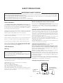
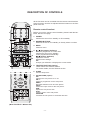
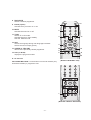
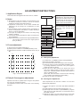
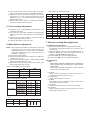
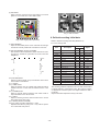
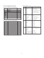
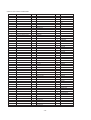
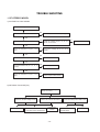
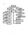
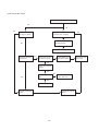
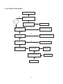
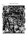
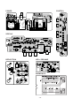
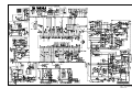
website:http://biz.LGservice.com
COLOR TV
SERVICE MANUAL
CHASSIS : CW62A
MODEL: 29FS2AL/ALX/BLX
MODEL: 29FS2AL/ALX/BLX-ZG
CAUTION
BEFORE SERVICING THE CHASSIS,
READ THE SAFETY PRECAUTIONS IN THIS MANUAL.
P/NO : MFL30504604
May., 2007
Printed in China
CONTENTS
Contents ...................................................................................................................2
Safety Precautions..............................................................................................3
Control Descriptions..........................................................................................4
Specifications........................................................................................................7
Adjustment Instructions .................................................................................8
Trouble Shooting ................................................................................................14
Printed circuit board.........................................................................................18
Block Diagram .....................................................................................................20
Exploded View....................................................................................................22
Exploded View Parts List .............................................................................23
Replacement Parts List .................................................................................24
SVC. Sheet..................................................................................................................
-2-
SAFETY PRECAUTIONS
IMPORTANT SAFETY NOTICE
Many electrical and mechanical parts in this chassis have special safety-related characteristics. These parts are identified by
in
the Schematic Diagram and Replacement Parts List.
It is essential that these special safety parts should be replaced with the same components as recommended in this manual to
prevent X-RADIATION, Shock, Fire, or other Hazards.
Do not modify the original design without permission of manufacturer.
General Guidance
Before returning the receiver to the customer,
An isolation Transformer should always be used during
the servicing of a receiver whose chassis is not isolated from
the AC power line. Use a transformer of adequate power rating
as this protects the technician from accidents resulting in
personal injury from electrical shocks.
always perform an AC leakage current check on the exposed
metallic parts of the cabinet, such as antennas, terminals, etc.,
to be sure the set is safe to operate without damage of
electrical shock.
Leakage Current Cold Check(Antenna Cold Check)
It will also protect the receiver and it's components from being
damaged by accidental shorts of the circuitry that may be
inadvertently introduced during the service operation.
If any fuse (or Fusible Resistor) in this TV receiver is blown,
replace it with the specified.
When replacing a high wattage resistor (Oxide Metal Film
Resistor, over 1W), keep the resistor 10mm away from PCB.
Keep wires away from high voltage or high temperature parts.
Due to high vacuum and large surface area of picture tube,
extreme care should be used in handling the Picture Tube.
Do not lift the Picture tube by it's Neck.
X-RAY Radiation
Warning:
The source of X-RAY RADIATION in this TV receiver is the
High Voltage Section and the Picture Tube.
For continued X-RAY RADIATION protection, the
replacement tube must be the same type tube as specified in
the Replacement Parts List.
To determine the presence of high voltage, use an accurate
high impedance HV meter.
With the instrument AC plug removed from AC source,
connect an electrical jumper across the two AC plug prongs.
Place the AC switch in the on position, connect one lead of
ohm-meter to the AC plug prongs tied together and touch other
ohm-meter lead in turn to each exposed metallic parts such as
antenna terminals, phone jacks, etc.
If the exposed metallic part has a return path to the chassis, the
measured resistance should be between 1MΩ and 5.2MΩ.
When the exposed metal has no return path to the chassis the
reading must be infinite.
An other abnormality exists that must be corrected before the
receiver is returned to the customer.
Leakage Current Hot Check (See below Figure)
Plug the AC cord directly into the AC outlet.
Do not use a line Isolation Transformer during this check.
Connect 1.5K/10watt resistor in parallel with a 0.15uF capacitor
between a known good earth ground (Water Pipe, Conduit, etc.)
and the exposed metallic parts.
Measure the AC voltage across the resistor using AC
voltmeter with 1000 ohms/volt or more sensitivity.
Reverse plug the AC cord into the AC outlet and repeat AC
voltage measurements for each exposed metallic part. Any
voltage measured must not exceed 0.75 volt RMS which is
corresponds to 0.5mA.
In case any measurement is out of the limits specified, there is
possibility of shock hazard and the set must be checked and
repaired before it is returned to the customer.
Leakage Current Hot Check circuit
Adjust brightness, color, contrast controls to minimum.
Measure the high voltage.
The meter reading should indicate
23.5 ± 1.5KV: 14-19 inch, 26 ± 1.5KV: 19-21 inch,
29.0 ± 1.5KV: 25-29 inch, 30.0 ± 1.5KV: 32 inch
If the meter indication is out of tolerance, immediate service
and correction is required to prevent the possibility of
premature component failure.
AC Volt-meter
To Instrument’s
exposed
METALLIC PARTS
Good Earth Ground
such as WATER PIPE,
CONDUIT etc.
0.15uF
1.5 Kohm/10W
-3-
DESCRIPTION OF CONTROLS
10
1
All the functions can be controlled with the remote control handset.
Some functions can also be adjusted with the buttons on the front
panel of the set.
Remote control handset
2
Before you use the remote control handset, please install the batteries. See the next page.
3
11
2. NUMBER BUTTONS
Switches the set on from standby or directly select a number.
PR
4
VOL
OK
3. MENU
selects a menu.
VOL
PR
13
1. POWER
switches the set on from standby or off to standby.
14
6
5
12
7
9
8
4.
D / E (Programme Up/Down)
selects a programme or a menu item.
switches the set on from standby.
scans programmes automatically.
F / G (Volume Up/Down)
adjusts the volume.
adjusts menu settings.
OK
accepts your selection or displays the current mode.
5. TELETEXT BUTTONS (option)
These buttons are used for teletext.
For further details, see the ‘Teletext’ section.
(With TELETEXT / PIP)
6. SLEEP
sets the sleep timer.
PR
VOL
OK
Q.VIEW
PR
VOL
LIST
5
UPDATE/
HOLD/
7. PIP BUTTONS (option)
PIP
switches the sub picture on or off.
PR +/selects a programme for the sub picture.
SWAP
alternates between main and sub picture.
INPUT
selects the input mode for the sub picture.
SIZE
adjusts the sub picture size.
STILL
freezes motion of the sub picture.
POSITION
relocates the sub picture in clockwise direction.
(With TELETEXT / Without PIP)
-4-
8. FAVOURITE
selects a favorite programme.
9. EYE/
1
10. MUTE
switches the sound on or off.
2
11. TV/AV
selects TV or AV mode.
switches the set on from standby.
exits the Teletext mode.
3
(option)
switches the eye function on or off.
*
10
11
PR
12. I/II/
*
selects the language during dual language broadcast.
selects the sound output (option).
4
VOL
Q.VIEW
13. Q.VIEW (or YELLOW)
returns to the previously viewed programme.
13
9
14. LIST (or BLUE)
6
OK
PR
VOL
LIST
14
8
displays the programme table.
12
* : No function
(Without TELETEXT / PIP)
COLOURED BUTTONS : These buttons are used for teletext (only
TELETEXT models) or programme edit.
PR
VOL
OK
VOL
PR
7
(With PIP / Without TELETEXT)
-5-
Front panel
3
VIDEO
4
1
25
L/MONO AUDIO R
6
ON/OFF
AV IN3
7
Side panel
1. MAIN POWER (ON/OFF)
switches the set on or off.
2. POWER/STANDBY INDICATOR
illuminates brightly when the set is in standby
mode.
dims when the set is switched on.
6. AUDIO/VIDEO IN SOCKETS (AV IN3)
Connect the audio/video out sockets of
external equipment to these sockets.
7. EYE (option)
adjusts picture according to the surrounding
conditions.
3. MENU
selects a menu.
4. OK
accepts your selection or displays the current
mode.
F / G (Volume Down/Up)
adjusts the volume.
adjusts menu settings.
D / E (Programme Up/Down)
selects a programme or a menu item.
switches the set on from standby.
5. REMOTE CONTROL SENSOR
Note : Only use the supplied remote control
handset. (When you use others, they’ll be not
able to function.)
-6-
SPECIFICATIONS
Note : Specification and others are subject to change without notice for improvement.
V
Scope
V
This specification can be applied to all the television related to
CW62A Chassis.
V
Test and Inspection Method
1) performance : Follow the Standard of LG TV test
2) Standards of Etc. requirement
- Safety: IEC60065
- EMC: EN55020,EN55013
V
Test Condition
1) Temperature : 20 ± 5°C(CST : 40 ± 5°C)
2) Relative Humidity : 65 ± 10%
3) Power voltage : AC110-240V~, 50/60Hz
4) Follow each drawing or spec for spec and performance of
parts,based upon P/N of B.O.M
5) Warm up TV set for more than 20min. before the
measurement.
General Specification
Item
No
1
Receiving System
Specification
PAL,SECAM BG
Remark
EU/ Non EU
PAL/SECAM DK
PAL-I/I
NTSC M
NTSC 4.43(AV)
SECAM-L/L’
OPTION
NTSC M/ PAL M/N
2
Available Channel
VHF : E2 ~ E12
Non EU/ EU
UHF : E21 ~ E69
CATV : S1 ~ S20
HYPER : S21 ~ S41
VHF : 02 ~ 13
NTSC-M
UHF : 14 ~ 69
CATV : 02 ~ 13
3
Input Voltage
AC 110-240V, 50/60Hz
AC 230V, 50/60Hz
EU
4
Market
EU,CIS, China, Asia, Africa
5
Screen Size
Flat 29”
6
Tuning System
FVS 100Program
7
Operating Environment
1) Temp : 0 ~ 45 deg
200 PR(W/O TXT)
2) Humidity : below 85%
8
Storage Environment
Non EU
1) Temp : -20 ~ 60 deg
2) Humidity : below 85%
-7-
ADJUSTMENT INSTRUCTIONS
1. Application Object
These instructions are applied to all of the color TV, CW62A.
CPT Assembling
As preparatory operations before
assembling CPT, wind cotton Tape for
protecting to CPT NECK and DY, CPT
connection parts. At this moment, end
of tape should be over-lapped and
wound in direct route to the NECK.
Assembling DY to
CPT
Fix the Magnet to the position as
shown picture below. Be careful not to
make CPT neck shadow while
adjusting DY.
2. Notes
(1) Because this is not a hot chassis, it is not necessary to use
an isolation transformer. However, the use of isolation
transformer will help protect test instrument.
(2) Adjustment must be done in the correct order.But the
adjustment can be changed by consideration of mass
production.
(3) The adjustment must be performed in the circumstance of
25±5°C of temperature and 65±10% of relative humidity if
there is no specific designation.
(4) The input AC voltage of the receiver must keep rating
voltage in adjusting.
(5) The receiver must be operated for about 15 minutes prior
to the adjustment.
(6) Signal: Received, the standard color signal.(65dB±1dB uV)
LG standard signal means the digital pattern
(PAL_EU 05CH).
HEAT RUN
Degaussing
6Pole
4
2
STC Pre-Adjustment
15 ~ 20mm
PURITY Adjustment
SCREEN Voltage adj.
Let the screen Standard condition.
Operate Heat-Run at least 15
minutes.
W/B Fixing
Torque is to be 9-11 kg f.cm when
fixing DY.
DY Fixing
3. Focus adjustment
(1) Receive the Cross-Hatch Pattern(Fig 1).
(2) Set the picture condition on “DYNAMIC(CLEAR)” mode.
(3) Adjust the Focus volume of FBT for the best focus of (A) &
(B).
A
Convergence Magnet
FOCUS not yet ADJ.
STC not yet ADJ.
B
DYC not yet ADJ.
4.1. Color purity adjustment
(1) It makes CPT or CABINET enough to demagnetization.
(2) Receive the signal of red raster.
(3) Loosen fixed screw of DY and closely to CPT funnel part.
(4) Check the center of screen that PURITY MAGNET of CPT
by crossing adjustment. At this time, 4 & 6 pole magnet is
located to magnet of nothing.
(5) Move the DY to make equal red on whole screen and it
does not to make the DY by fixed screw after check a
simple color of Red/Green/Blue and white raster whether or
not it is a pollution of color.
(At this time, take care raster of screen and DY must fixing
in the condition which maintains a horizontality.)
(6) Check the TV set by move direction.
<Fig 1. Cross-Hatch Pattern(E-7CH)>
4. Purity & Convergence adjustment
4.2. Convergence adjustment
Adjustment should be operated when using the CPT(without
ITC from CPT manufacturing place)
This adjustment must be done in the order of the following
flowchart.
These adjustments can the best condition of focus after
finished purity adjustment.
(1) Receive the signal of cross hatch that BACK RASTER is
black.
(2) Adjust brightness and luminosity till dot appear 9 ~12.
(3) Open angle of the two tab of 4 pole MAGNET by isogonic
angle and accord with vertical line of red and blue color in
the middle of screen.
(4) Maintain as angle of (3) and rotate the tab to accord with
vertical line of Red and Blue color in the middle of screen.
-8-
2. White balance IIC Parameter(Address)
(5) Open angle of the two tab of 6 pole magnet by isogonic
angle and accord with vertical line of Red/Blue and Green.
(6) Maintain as angle of (5) and rotate the tab to accord with
horizontal line. In case of twisted horizontal line,repeat
adjustment of (3) ~ (5) remembering the movement of
Red/Green/Blue color.
(7) Move the DY to best condition of convergence and attach
the CPT to a rubber-chock for fixing DY.
Program Win31_wb
Vcd Slave
8A
B(R)_Amp
Program
5. Screen voltage adjustment
(1) Receive the PAL or SECAM(NTSC) signal into RF mode
(regardless of channel).
(2) If you press the “ADJ”button in LINE SVC mode(IN-START
button),the LINE SVC mode changes to screen adjustment
mode.
(3) Turn the Screen Volume of FBT to change luminance of
White signal center as shown below.
(4) Press the ADJ button to exit SVC mode.
TWB
Win31_wb TWB
Eeprom_Slave
B(R)_Cut
A0
G_Amp
Win31_wb TWB Win31_wb TWB Win31_wb
Speed Delay
1
30
G_Cut
TWB Win31_wb TWB
Sub Add
20
17
21
18
Start Bit
5
5
5
5
Stop Bit
0
0
0
0
Offset
0
0
2
2
Polarity
1
1
0
0
EP_Rom_S
36
33
37
34
Speed/ Plus
2
2
2
2
7. Deflection setting Data Adjustment
6. White balance adjustment
7.1 Adjustment preparation
NOTE : When adjusting white balance automatically,connect the
adjustment JIG in SVC mode.(When pressing INSTART,MUTE button on remote control for adjustment
orderly,it is changed to CPU OFF mode and screen is
displayed to “CPU OFF”.)
(1) Receive 100% white pattern.
(2) Adjust LOW Light status(4.5FL) of CR(R CUT), CB(B CUT)
at CG(G CUT:75) : 60.
(3) Adjust HIGH Light status(35FL) of WR(R DRIVE), WB(B
DRIVE) at WG(G DRIVE:380) : 450.
(4) Repeat above step (2) and (3) for the best condition each
status of High Light and Low Light.
(1) Tune the TV set to receive an Digital pattern(EU05CH).
(2) Deflection setting data adjustment is operate by SVC
communicator.
(3) Enter the deflection mode by selection SERVICE2 key on
SERVICE MENU after enter the adjustment mode by
pressing LINE SVC MODE(IN-START KEY).
(4) Use the CH D ,E key to select adjustment item.
(5) Use the VOL F ,G key to increase/decrease data.
7.2 Adjustment
<Table 1> White Balance Color analyzer
Menu
EU
N-EU
X
288
268
Y
295
273
Color Temperature
9000oK
13000oK
(1) H SHIFT
Adjust so that the geometric horizontal center line is in
accord with horizontal center line of CPT.
(2) H PARALLEL
Adjust vertical inclination of screen.
(3) H BOW
After finishing Cushion adjustment, adjust curved rate of
top & bottom corner to be equal.
(4) V LINEAR
Adjust the top & bottom size of inner circle to be equal.
(5) V SCROLL
Adjust so that the geometric vertical center line is in accord
with vertical center line of CPT.
<Table 2> White Balance Initial Data
LOW LIGHT
HIGH LIGHT
Menu
Range
DATA
BLO-R(R CUT)
0 ~ 63
32
BLO-G(G CUT)
0 ~ 63
32
BLO-B(B CUT)
0 ~ 63
FIX
RG(R DRIVE)
0 ~ 63
32
GG(G DRIVE)
0 ~ 63
32
BG (B DRIVE)
0 ~ 63
32
<Table 3> White Balance Initial Data
1. IC
Name
Maker
Algorithm
VCD IC
EP_ROM
0
0
0
<Note>
- When adjusting a deflection,adjust N50Hz of PAL signal first and
adjust a deflection data at N60Hz(NTSC), Z60Hz, N50Hz,
W50Hz, Z50Hz.
- After finishing deflection adjustment, press the ENTER
button to enter or exit SVC mode.
0
-9-
(6) EW WIDTH
Adjust until the outmost left and right lattice of received
pattern is accord with 25% of other lattice width.
<Fig. 4> PIP H Position
8. Deflection setting initial data
<Fig. 2>PAL Digital pattern (EU05CH)
(7) EW PARABOLA
Adjust so that middle portion of the outermost left and right
vertical line look like parallel with vertical lines of the CPT.
<Table 4> Deflection setting initial data (SERVICE 2)
* Fix : Don’t change data
Item
(8) EW UPCORNER & (9) EW LOCORNER
After finished cushion adjustment, adjust vertical line of lefttop, right-top, left-bottom, right-bottom of screen to the best
straight line.
H-SHIFT
H PARALL
CRNU
EP
CRNL
CRNL6
<Fig. 3> Cross-Hatch Pattern(E-7CH)
(10) EW TRAPEZOID
Adjust to make the length of top horizontal line same with it
of the bottom horizontal line.
(11) V SLOPE
(12) V AMPLITITUE
Adjust so that the circle of a digital circle pattern should be
located interval of 6~7mm from the effective screen of the
CPT.
(13) S CORRECTION
Adjust so that all distance between each lattice width of
top/center/bottom are to be the same.
(14) V SHIFT
Adjust so that the geometric vertical center line is in accord
with vertical center line of CPT.
(15) V ZOOM (VERTICAL ZOOM)
(16) PIP_H(PIP H Position) adjustment - option
Adjust the H-Position by using VOL +/- key until PIP picture
is in contact with main picture.
29”
50Hz 60Hz
Adjust
Horizontal shift
24
34
Adjust
Horizontal parallelogram
32
32
Recommend
Bow
32
32
Recommend
V LINEAR
Vertical linearity
41
44
Recommend
V SCROLL
Vertical scroll
30
30
Adjust
EW WIDTH
EW width
57
57
Adjust
EW PARAB
Parabola adj
18
15
Adjust
EW UPCOR Upper corner adj
49
45
Adjust
EW LOCOR Lower corner adj
53
50
Adjust
H BOW
CRNU6
Description
EW TRAPE
Trapezoid adj
25
25
Adjust
V SLOPE
Vertical slope
17
25
Recommend
V AMPLIT
Vertical amplitude
34
29
Recommend
SCORRECT S correction
35
30
Recommend
V SHIFT
Vertical shift
46
54
Recommend
V ZOOM
Vertical zoom
25
25
Fix
V SYNSLI
Vertical slicing level
0
0
Fix
Over voltage input mode
0
0
Fix
Vertical guard mode
0
0
Fix
OVRVOLIN
VGUARD
- After finishing deflection adjustment at PAL 50Hz, NTSC 60Hz
is applied deflection compensation value. But recheck condition
of adjustment at NTSC system and adjust deflection data if
necessary.
- Adjust PIP Position adjustment at only PAL 50Hz.
- 10 -
<Table 7> OPTION 1, 2, 3, 4
9. Service adjustment data table
ITEM
<Table 5> Picture setting service data1 (SERVICE 1)
ITEM
DESCRIPTION
OPTION1
29” S-SLIM
Description
INCH
29 S-Slim/ 29 N-Flat
SYSTEM
BG/DK/I/M, BG/DK/I/L
ACG take over
25
200PR
W/O TXT=>200PR, W/TXT=>100PR
RG
Red Gain
32
TOP
TOP=>Germany, Swiss, Austria, Italy
GG
Green Gain
32
ACMS
Auto channel memory system
BG
Blue Gain
32
CH-AU
China & Australia Frequency table
BLO-R
Black level offset Red
32
BLO-G
Black level offset Green
32
Cathode Drive Level
5
L-DLY
Luminance delay time
13
PEAK
Peak white limiting
SHOOT
Pre overshoot ratio
AGC
CDL
BOOSTER
OPTION2
SOUND
RF stereo / AV stereo / Mono option
PIP
PIP option
VOL CURVE
High / Low volume curve
1
A2 STEREO
Nicam check & FM stereo / Dual
1
I/II SAVE
Dual sound setting save
HIDEVIAT (High deviation)
Sound high deviation
SCART
SCART option
DVD
DVD option
XWAVE
FM TX option
EYE
EYE option
4KEY
4 Key option
TILT
TILT option
DEGAUSS (Degaussing)
Degaussing option
OSD LANG
Refer to the next page(table.8)
TXT LANG
Refer to the next page(table.8)
<Table 6> Picture setting service data2 (SERVICE 3)
ITEM
DESCRIPTION
OPTION3
29” S-SLIM
AM DEM G
AM DEMODULATOR GAIN-AMLOW
0
FM DEM G
FM DEMODULATOR GAIN-AGN
0
ADC LEV
ADC LEVEL(-16~5) - ADCLEV
0
DEC LEV
DEC LEVEL(-16~5) - DECLEV
0
MONO LEV
MONO LEVEL(-16~5) - MONOLEV
0
NICAMLEV
NICAM LEVEL(-16~5) - NICLEV
0
AUX1 VOL
AUX1 VOL - AUX1VOLL(R)
0
AUX2 VOL
AUX2 VOL - AUX2VOLL(R)
0
AUX3 VOL
AUX3 VOL(SCART1 RF SOUND OUT)
0
FMWINDOW FM WINDOW FILTER (FMWS)
BOOSTVAL
MAXVOL
DCXO VAL
BOOSTER
OPTION4
REMOCON
0
0
MAX VOLUME
100
DCXO
63
HOTEL
HOTEL option
TURBOSCH (Turbo search)
Turbo search
TURBOP/S (picture/sound)
Turbo picture/ sound
DCXO/A (DCXO auto adjust) DCXO auto adjust
- 11 -
<Table 8> OSD & TEXT LANGUAGES
0
SOUTHEAST ASIA
0
ENGLISH
1
1
EAST EU CYRILLIC TEXT
2
RESERVED
3
RESERVED
4
RESERVED
5
RESERVED
6
RESERVED
7
RESERVED
0
ENGLISH
1
EAST EU ALL
2
3
WEST EU GREEK TEXT
ENGLISH RUSSIAN
3
RESERVED
4
RESERVED
5
RESERVED
6
RESERVED
7
RESERVED
0
ENGLISH
1
EU 7EA
2
3
WEST EU ALL
ENGLISH GREEK
4
RESERVED
5
RESERVED
6
RESERVED
7
RESERVED
- 12 -
0
ENGLISH
1
INDONESIAN
2
MALAY
3
VIETNAMESE
4
THAI
0
ENGLISH
1
GERMAN
2
RUMANIAN
3
POLISH
4
HUNGARIAN
5
CZECH
6
RUSSIAN
7
BULGARIAN
0
ENGLISH
1
RUSSIAN
0
ENGLISH
1
GERMAN
2
FRENCH
3
ITALIAN
4
SPANISH
5
DUTCH
6
PORTUGUESE
0
ENGLISH
1
GERMAN
2
FRENCH
3
ITALIAN
4
SPANISH
5
DUTCH
6
SWEDISH
7
NORWEGIAN
8
DANISH
9
FINNISH
10
PORTUGUESE
11
GREEK
0
ENGLISH
1
GREEK
3
ARAB TEXT
0
ENGLISH
1
ARABIC
2
3
PARSI
ARAB ALL
4
RESERVED
5
RESERVED
6
RESERVED
7
RESERVED
4
PARSI TEXT
The same ARAB TEXT
5
SOUTHEAST W/O TEXT
The same SOUTHEAST ASIA TEXT
6
WEST EU W/O TEXT
The same WEST EU GREEK TEXT
7
EAST EU W/O TEXT
The same EAST EU CYRILLIC TEXT
8
ARAB W/O TEXT
9
CHINA, INDIA W/O TEXT
0
ENGLISH
1
FRENCH
2
ARAB
3
URDU
0
ENGLISH
1
FRENCH
2
ARAB
3
PARSI
0
ENGLISH
1
FRENCH
2
ARAB
3
URDU
4
PARSI
0
ENGLISH
1
CHINESE
0
ENGLISH
1
HINDI
The same ARAB TEXT
0
ENGLISH
1
CHINA
2
HINDI
3
RESERVED
4
RESERVED
5
RESERVED
6
RESERVED
7
RESERVED
10. How to inspect condition of a
transmission and reception in FM
TRANSMISSION MODEL
11.OPTION Adjustment
- FM TRANSMITTER’s efficiency inspections is executed to a
finished in a final inspection phase.
- FM TRANSMITTER is a function which receives voicesignal by an exclusive remote control and Earphone, transmits
a FM through transmitter of inner part in MICOM BOARD to
TV sound(MONITOR OUTPUT)
1) Execute in channel generating voice-signal
2) Select a transmitted frequency in MENU OSD.
MENU => SOUND => TRANSMITTER => frequency
selection (87.7MHz)
3) A received frequency in an exclusive remote control or
received FM Radio is tuned by 87.7MHz(107.7MHz) which
is same as frequency in OSD.
4) Check out whether a signal generating to MAIN SPEAKER
generates in earphone or receiver or not.
5) There is no alternation and setting of adjusted DATA in the
process of inspecting FM TX.
1) This option adjustment decides function in accordance with
model. Press IN-START button at SVC mode, then adjust
the option at OPTION1,2,3,4,5 mode.
2) Mark the option adjustment data like [112,68,164,32,8] in
BOM.
* Mark of BOM
LEVEL PART NO.
SPECIFICATION
1. 3141VMN382A MAIN CHASSIS ASSY
DESCRIPTION
[112,68,164,32,8]
In this model, the OPTION1 data is 112, OPTION2 data is 68, the
OPTION3 data is 164,the OPTION 4 data is 32, OPTION 5 data
is 8.
- 13 -
TROUBLE SHOOTING
1. RF-STEREO MODEL
1) PICTURE OK / NO SOUND
Selected correct system in menu
OK
NO
Check the waveform IF 1 of TU101
Check/ Replace TU101 or Input signal
OK
NO
Check the waveform at pin 4, 5 of IC501
Check the voltage at pin 3, 9, 16, 43,
86, 88, 90 of UOCIII
NO
Check/ Replace IC501
OK
Check the waveform at pin 4, 12 of
IC601
NO
Check the voltage at pin 57, 58 of
UOCIII
OK
NO
Check the waveform at pin 6 of IC601
Check/ Replace Q603
OK
Check the waveform at pin 1, 2, 14, 15
of IC601
NO
Check/ Replace IC601
OK
Check the waveform at pin 3, 13 of
IC601
NO
Check/ Replace R823, D826
2) No Raster / Sound OK(1/2)
Check the Heater voltage of
CPT(6~6.4 Vrms)
Check HV, Screen voltage of CPT
Check FBT T402
Check R, G, B out of CPT board
Check 197V line of CPT Board &
if no problem check and Replace
Check IC901,
P402A
- 14 -
Check the Heater pulse of FBT T402
Check RF901, P402,
P402B, FR401
Check FBT T402
3) No Raster (2/2)
Check the B+ at D829
cathode
Normal
Is the voltage each
pin voltage of IC501
Abnormal
OPEN
NO
Check Fuse of AC line
Check/ Replace Fuse
OK
Check pin 73 of
IC501(H_Out)
Check the in/out of
regulator(IC822,
IC823, IC824)
Check the voltage of
C832
Check/ Replace
IC501
NO
Check/ Replace DB801
Check Q402
collector waveform
Check the voltage
pin4 of IC810
Check/ Replace
Q402
NO
Check/ Replace Fuse and IC810
Check T401 & each
pin voltage
Check/ Replace
IC810, IC802, Q830
Check/ Replace
T401
Check Q401 collect
waveform
NO
Check Fuse and Diode of secondary
Load of SMPS trans(T801)
Check/ Replace
Q401
OK
Check & Replace
T402
Check/ Replace IC501
- 15 -
4) No Picture/ No Sound
Is any OSD displayed?
NO
OK
OK
Check IC501 pin 83,
84, 85 (R, G, B out)
Check receiving system in MENU
& execute Auto - Program
OK
Does the auto - Program
operate properly
NO
OK
Store on manual -program MENU
NO
Check the waveform
pin73(H-out)
NO
Check IC501 pin 83,
84, 85 (R, G, B out)
Check SMPS Trans
Secondary Voltage
OK
Check pin3 Reset
Voltage
OK
OK
Check pin8, 12 SCL,
SDA
NO
Check IC12(EEPROM)
& SCL, SDA, Line
OK
Replace IC501
P13A (R, G, B out of
IC501)
P13A (R, G, B out of
IC501)
- 16 -
Go to No sound/
picture OK
2. AV STEREO/ MONO MODEL
Select correct system in menu
OK
OK
Check the connection of AV
equipment
AV
Does the auto - Program
operate properly
OK
Check TU101 Tuner
OK
NO
Check the waveform at
pin57, 58 of IC501
Check the voltage of pin3, 9,
16, 43, 86,88,90 of IC501
OK
NO
Check the waveform at
pin4, 12, of IC601
Check the signal line of SPK-N,P
OK
NO
Check the waveform at
pin6 of IC601
Check pin5 (mute) of IC501
OK
Check the waveform at
pin1, 2, 14, 15 of IC601
NO
Check the voltage at
pin3, 13, of IC601
NO
Check/ Replace
R823, D826
OK
Check the connection of side
or Front AV Board P201A
OK
Replace IC601
- 17 -
NO
Correct the Board
PRINTED CIRCUIT BOARD
MAIN
- 18 -
POWER
CONTROL
SIDE-A/V
DEFLECTION
LED + PRE-AMP
HARMONICS
- 19 -
BLOCK DIAGRAM
- 20 -
MEMO
- 21 -
EXPLODED VIEW
943
400
913
170
150
112
P1112
503
Option
520
550
580
501
540
331
300
330
120
320
590
600
530
310
- 22 -
EXPLODED VIEW PARTS LIST
LOCA. No.
112
PART No.
6335929005A/L
EAK32601101/02
120
6400VA0025E
150
6140VC2007F/T/Z
EAB30828501
170
170-844K
300
30919K0017E
30919K0019B/R
310
The components identified by mark
critical for safety.
Replace only with part number specified.
DESCRIPTIONS
CPT,ITC A68ERS870X 02 N(+0.40G) 0G LG-PHILIPS DISPLAYS 29INCH 1H SUPER SLIM
CPT,ITC A68QGU870X L 29INCH SUPER-SLIM +0.5G 4/3 60HZ 6150Z-9245A
Speaker,Fullrange C163A01K1451 FERRITE 15W 8OHM 86DB 110HZ 193X57X44.4mM LUG
Speaker,Fullrange C163A01K1451. ND 15W 8OHM 86DB 110HZ 193 X 57 X 44.4 LUG
Coil,Degaussing 23OHM AL 80T 0.65mM SQUARE 29INCH 3250mM WIRE=300mM
Drawing,Assembly CPT EARTH UL1015 AWG22-TBC 0.12X4X16MM 29INCH ALL NORMAL
Cover Assembly, 29FS2BLX-ZG CW62A 29” SY-RA RA TOOL CW62A 50HZ SKD 1TONE
Cover Assembly, 29FS2 MA MC049D 29” 29FS2 C/A ASSY LGEMA
ACQ30285802
Cover Assembly, 29FS2 CW62A 29” LGESY 2-TONE W/O EYE SY-CIS #117A SKD
30919K0019H
Cover Assembly, 29FS2BLX CW62A 29"" 117A LGEMA TOOL ASSY
ACQ30285811
Cover Assembly, 29FS2 CW62A 29"" LGESY 2-TONE W/O EYE
5020900039B
Button, CONTROL 29FS2 ABS, HF-380 6KEY LGESY LOCAL 117A
5020900088B
Button, MOLD ABS CONTROL 29FS2 ABS, HF-380 6KEY LGERA
5020900094A/B
Button, MOLD ABS 380 CONTROL 29FS2 ABS, HF-380 6KEY LGEMA
320
320-062E
330
5020900038B
Button, POWER 29FS2 ABS, HF-380 1KEY LGESY LOCAL 117A
5020900087B
Button, MOLD ABS POWER 29FS2 ABS, HF-380 1KEY LGERA B/POWER
331
5020900093A/B/C
Button, MOLD ABS 380 POWER 29FS2 ABS, HF-380 1KEY LGEMA
4810900096A
Bracket, BOTTOM 29FS2 MC035E HIPS LGERA BRACKET POWER
4810900099A/B
Bracket, MOLD HIPS BOTTOM 29FS2 MC05HB HIPS 51SF LGEMA
4810900051B
400
501
503
520
Spring, CUTTING STSC304 KNOB
Bracket NON 29FS2 MC036A ABS, HF-380 LGESY LOCAL 117A
3809900145L/P
Cover Assembly, 29FS2ALX CW62A 29” SY-CLS CW62A SKD #117
3809900193C
Cover Assembly, 29FS2ALX CW062A 29”” SY-RA RA TOOL CW62A
3809900199D
Cover Assembly, 29FS2 LGEMA CW62A 29” 29FS2 B/C ASSY LGEMA
4810900052D
Bracket, MAIN 29FS2 MC049D HIPS 407AF LGESY LOCAL 50HZ CUT RIB
4810900101A
Bracket, MOLD HIPS 40AF MAIN 29FS2 MC05HB HIPS 405AF LGEMA
4810900100D/F
Bracket, MOLD HIPS REAR AV 2PHONE 29FS2 CW62A HIPS 51SF LGEMA LOCAL
4810900104B
Bracket, REAR AV 29FS2RLX-TG CW62A HIPS 51SF LGESY LOCAL
EBR30755601
PCB Assembly, MAIN1 M.I CW62A 29FS2ALX-ZG QDRLLBK SY TO KIEV
EBR30770317/18
PCB Assembly, MAIN1 M.I CW62A 29FS2AL-ZG QDKLLBA SY TO LGEAK SKD 6871
EBR30770341/54
PCB Assembly, MAIN1 M.I CW62A 29FS2BLX-ZG QRULLCU SY TO LGERA SKD 6871
EBR30921805/06/07/08
EBR30769926
PCB Assembly, MAIN1 M.I CW62A 29FS2ALX SY-MA-ROMANIA SKD
PCB Assembly, MAIN1 M.I CW62A 29FS2AL-ZG. QDKULBA SY -AK
EBR30921909
PCB Assembly, MAIN1 M.I CW62A 29FS SY-TTE TS CPT
530
EBR30756001
PCB Assembly, MAIN1 M.I CW62A 29FS2 SY TO CIS SUPER SLIM CONT BOARD
EBR30924202
PCB Assembly, SUB M.I CW62A 29FS2 CONTROL SY-MA SKD
540
EBR30756601
PCB Assembly, MAIN1 M.I CW62A 29FS2 SY TO CIS SUPER SLIM POWER BOARD
EBR30924002
PCB Assembly, SUB M.I CW62A 29FS2 POWER SY-MA SKD
550
68719SM219A
PCB Assembly, SUB M.I MC049D SY-MA HARMONICS CKD
EBR30691901
PCB Assembly, MAIN1 M.I CW62A 29FB3 SY TO CIS SKD MODEL HANMONIC BOARD
580
EBR30924403
PCB Assembly,SUB M.I CW62A 29FS2 HARMONIC BOARD
EBR30683001
PCB Assembly, MAIN1 M.I CW62A 29FS4 SY TO CIS SKD DEFLECTION BOARD
EBR30923602
PCB Assembly, SUB M.I CW62A S/S DEFLECTION SY-MA-POLAND SKD
EBR30683003
PCB Assembly, Deflection SUB M.I CW62A 29FS SY TO CE NATION
590
EBR30758201
PCB Assembly, MAIN1 M.I CW62A SY TO CIS SUPER SLIM LED+PRE AMP BOARD
EBR30924402
PCB Assembly, SUB M.I CW62A 29FS2 LED+P-AMP SY-MA SKD
600
EBR30757201
PCB Assembly, MAIN1 M.I CW62A 29FS2 SY TO CIS SUPER SLIM SIDE AV
EBR30923802
PCB Assembly, SUB M.I CW62A 29FS2 SIDE A/V SY-MA SKD
913
FAB30021506
Screw Assembly, FAB30021506 TAPTITE P TYPE D7.0 L45.0 RUBBER
943
FAB30006309
Screw,Taptite 1SZZ9PB012A TH + P 4MM 16MM MSWR10 FZB
P1112
174-009E/P
Power Cord Assembly, CE-503/H03VVH2-F 2X0.75MM2/2.4M/BLK CE-503 TJC1-2Y
6410VEH001B
Power Cord Assembly, CE-503/H03VVH2-F 2X0.75MM2/2.4M/BLK CE-503 TJC1-2Y
- 23 -
is
REPLACEMENT PARTS LIST
For Capacitor & Resistors,
the characters at 2nd and 3rd
digit in the P/No. means as
follows;
LOCA. NO
CC, CX, CK, CN : Ceramic
CQ : Polyester
CE : Electrolytic
PART NO
RD : Carbon Film
RS : Metal Oxide Film
RN : Metal Film
RF : Fusible
DESCRIPTION
LOCA. NO
PART NO
D406
0DRTW00164B
RGP15J 600V 1.3V 5UA 50A 250NSEC DO15
D407
0DD060009AC
TVR06J 600V 1.4V 10UA 25A 300NSEC DO41
AT24C16A-10PI-2.7 16KBIT 2KX8BIT 2.7VTO5.5V
D414
0DRTW00164B
RGP15J 600V 1.3V 5UA 50A 250NSEC DO15
IC
DESCRIPTION
IC12
0IAL241610B
IC301
0IPMGPH002A
TDA4863A 9.0VTO30.0V - 3.2W - DBS ST 7P
D444
0DD060009AC
TVR06J 600V 1.4V 10UA 25A 300NSEC DO41
IC302
0IKE455800E
KIA4558 36V_+-18V 6mV - - 500MW 30uV/V
D606
0DD414809ED
1N4148 1V 100V 150MA 500MA 4NSEC 500MW
IC601
0ILNR00189A
TDA7297SA 6TO18V 0 0.10% 15W 30W 56DB
D815
0DD414809ED
1N4148 1V 100V 150MA 500MA 4NSEC 500MW
IC802
0ILI817000G
LTV-817M-VB 6V 35V 35V 50MA 100NA
D818
0DD060009AC
TVR06J 600V 1.4V 10UA 25A 300NSEC DO41
IC810
0IPMG78443A
STR-X6556 16.2TO19.4V - - ZIP ST 7P
D820
0DD060009AC
TVR06J 600V 1.4V 10UA 25A 300NSEC DO41
IC823
0IMCRAU004A
S1117-33PIC 4.8TO12V 3.3V 2W TO220 ST 3P
D823
0DRTW00141A
SFAF504G 200V 975MV 10UA 125A 35NSEC
IC824
0IMCRKE020A
KIA78S06P 8.1TO21V 6V 600MW TO92 ST 3P
D826
0DRTW00141A
SFAF504G 200V 975MV 10UA 125A 35NSEC
IC826
0IMCRKE018A
KIA78R05API 6TO12V 5V 1.5W TO220IS ST 4P
D828
0DD060009AC
TVR06J 600V 1.4V 10UA 25A 300NSEC DO41
IC901
0IPRP00747A
TDA6107AJF 180TO210V 6mA - SIP ST 9P
D829
0DD410000AD
RU4AM 600V 1.3V 10UA 70A 400NSEC R4
Q602
0IFA754207A
KA75420ZTA(KA7542ZTA) 0.3TO15V 4.2V
D845
0DZ150009AD
MTZJ15B 15V 13.89TO14.62V 25OHM 500MW
Q830
0IMCRFA007A
KA431AZ 2.47TO2.52V 36V 770MW TO92 TP
D846
0DD400509BB
UF4005(52MM) 600V 1.7V 10UA 30A 75NSEC
D847
0DD060009AC
TVR06J 600V 1.4V 10UA 25A 300NSEC DO41
D901
0DD060009AC
TVR06J 600V 1.4V 10UA 25A 300NSEC DO41
TRANSISTOR
Q105
0TR102009AB
KRC102M(KRC1202) NPN 30V - 50V 100MA
D902
0DD060009AC
TVR06J 600V 1.4V 10UA 25A 300NSEC DO41
Q1106
0TR733009AA
KSA733C-Y PNP -5V -60V -50V -0.15A
D903
0DD060009AC
TVR06J 600V 1.4V 10UA 25A 300NSEC DO41
Q201
0TR198009BA
2SA1980Y PNP -5V -50V -50V -0.15A
D904
0DR140049AC
1N4004A 500V 1.1V 10UA 30A - DO41
Q204
0TR198009BA
2SA1980Y PNP -5V -50V -50V -0.15A
DB801
0DRTW00131C
TS6P05G 600V 1V 5UA 150A TS6P ST 4P 4
Q301
0TR198009BA
2SA1980Y PNP -5V -50V -50V -0.15A
ZD101
0DZ330009DG
GDZJ33B 33V 30.32TO31.88V 65OHM 500MW
Q302
0TRKE10013A
KTD1047 NPN 6V 160V 140V 12A 100UA
ZD401
0DZ510009BE
GDZ5.1B 5.1V 4.94TO5.2V 20OHM 500MW
Q303
0TR127409AB
KTA1274-Y PNP -5V -80V -80V -0.4A
ZD401
0DZ510009BF
GDZ5.1B 5.1V 4.94TO5.2V 20OHM 500MW
Q401
0TRSA10005A
2SC6090LS NPN 5V 1.5KV 700V 10A 10UA
ZD402
0DZ120009AF
MTZJ12B 12V 11.44TO12.03V 25OHM 500MW
Q402
0TR437000BA
KTC4370A-Y NPN 5V 180V 180V 1.5A 1UA
ZD501
0DZ510009DB
MTZJ5.1B 5.1V 4.94TO5.2V 70OHM 500MW
Q502
0TR198009BA
2SA1980Y PNP -5V -50V -50V -0.15A
ZD502
0DZ820009AH
MTZJ8.2B 8.2V 7.78TO8.19V 20OHM 500MW
Q503
0TR319809AA
KTC3198(KTC1815) NPN 5V 60V 50V 150MA
ZD601
0DZ820009AH
MTZJ8.2B 8.2V 7.78TO8.19V 20OHM 500MW
Q504
0TR319809AA
KTC3198(KTC1815) NPN 5V 60V 50V 150MA
ZD827
0DZ750009AG
MTZJ7.5B 7.5V 7.07TO7.45V 20OHM 500MW
Q505
0TR127009AA
KTA1270-Y(KTA562TM) PNP -5V -35V -30V
ZD910
0DZ510009BE
GDZ5.1B 5.1V 4.94TO5.2V 20OHM 500MW
Q506
0TR127009AA
KTA1270-Y(KTA562TM) PNP -5V -35V -30V
ZD910
0DZ510009BF
GDZ5.1B 5.1V 4.94TO5.2V 20OHM 500MW
Q603
0TR534309AA
2SC5343Y NPN 5V 60V 50V 150MA 100NA
ZD911
0DZ510009BE
GDZ5.1B 5.1V 4.94TO5.2V 20OHM 500MW
Q803
0TR102009AB
KRC102M(KRC1202) NPN 30V - 50V 100MA
ZD911
0DZ510009BF
GDZ5.1B 5.1V 4.94TO5.2V 20OHM 500MW
Q804
0TR534309AA
2SC5343Y NPN 5V 60V 50V 150MA 100NA
ZD912
0DZ510009BE
GDZ5.1B 5.1V 4.94TO5.2V 20OHM 500MW
Q805
0TR102009AB
KRC102M(KRC1202) NPN 30V - 50V 100MA
ZD912
0DZ510009BF
GDZ5.1B 5.1V 4.94TO5.2V 20OHM 500MW
Q806
0TR127409AB
KTA1274-Y PNP -5V -80V -80V -0.4A
Q809
0TR319809AA
KTC3198(KTC1815) NPN 5V 60V 50V 150MA
Q810
0TR319809AA
KTC3198(KTC1815) NPN 5V 60V 50V 150MA
C103
0CE475DK618
EGR475M050T1G1C11G 4.7uF 20% 50V 50MA
Q811
0TR534309AA
2SC5343Y NPN 5V 60V 50V 150MA 100NA
C107
0CE227DD618
EGR227M010T1G1E11G 220uF 20% 10V 255MA
Q840
0TR421009CA
BF421 PNP -5V -0.3KV -0.3KV -0.05A
C108
0CE475DK618
EGR475M050T1G1C11G 4.7uF 20% 50V 50MA
C109
0CE226DK618
SMS5.0TP50VB22M 22uF 20% 50V 108MA
C1103
0CE4763F618
ESF476M016T1A5E05G 47uF 20% 16V 60MA
CAPACITOR
DIODE
D101
0DD414809ED
1N4148 1V 100V 150MA 500MA 4NSEC 500MW
C1111
0CQZVBK002C
PCX2 335 91592 0.22uF 10% 275V MPP
D102
0DSVH00019A
BA282 1V 35V 100MA
C112
0CN1030F679
RH EP050 Y103M-B-B 10nF 20% 16V X5R
D11
0DD414809ED
1N4148 1V 100V 150MA 500MA 4NSEC 500MW
C113
0CN1030F679
RH EP050 Y103M-B-B 10nF 20% 16V X5R
D301
0DD400509AA
1N4005 600V 1.1V 5UA 30A - DO41
C115
0CN1040K949
CH UP050 F104Z-B-B Z 100nF -20TO+80%
D302
0DD414809ED
1N4148 1V 100V 150MA 500MA 4NSEC 500MW
C1201
0CN4710K519
RH UP050 B471K-B-B 470pF 10% 50V Y5P
D401
0DRSA00211A
FMV-205GUR 1.7KV 1.7V 50UA 50A 600NSEC
C1202
0CN4710K519
RH UP050 B471K-B-B 470pF 10% 50V Y5P
D403
0DD414809ED
1N4148 1V 100V 150MA 500MA 4NSEC 500MW
C1409
0CF4342U460
PCMP 389 52434 0.43UF 5% 400V MPP
D405
0DRTW00164B
RGP15J 600V 1.3V 5UA 50A 250NSEC DO15
C1410
181-013M
@@@@@@@@@@f
W2@@6Xh
W&h
?W&@@@@)X?g
?W&@h
?7(M?I'@1?g
W&@@h
?@H?eN@@?g
?W.Y@@h
?@f?@@?g
W.Y?@@h
?@@?g
?W.Ye@@h
J@5?g
O.Y?e@@h
7(Y?g?@@@@@@@@@@@g
?@@Yf@@h
?J(Yh
W.Y?h
?@@@@@@@@@@@g
?W.Yhe
@@h
W.Y?e@?g
@@h
?W&Yf@?g
@@h
W&@@@@@@@?g
@@h
&@@@@@@@@?g
@@h
@@@@@@@@@@f
MPP224J2GD 220nF 5% 400V MPP
For Capacitor & Resistors,
the characters at 2nd and 3rd
digit in the P/No. means as
follows;
LOCA. NO
PART NO
C1421
181-010H
C1479
C1490
DESCRIPTION
CC, CX, CK, CN : Ceramic
CQ : Polyester
CE : Electrolytic
RD : Carbon Film
RS : Metal Oxide Film
RN : Metal Film
RF : Fusible
LOCA. NO
PART NO
PPN393K2GH 39nF 10% 400V PP
C501
0CF2241L438
PCMT 365 76224 220nF 5% 63V MPE
0CF4342U460
PCMP 389 52434 0.43UF 5% 400V MPP
C502
0CE225DK618
EGR225M050T1G1C11G 2.2uF 20% 50V 20MA
0CF7041R460
PCMP389 42704 0.7uF 5% 250V MPP
C503
0CQ6821N509
PEI682K2AT 6.8nF 10% 100V PE -40TO+85C
C17
0CN1030F679
RH EP050 Y103M-B-B 10nF 20% 16V X5R
C504
0CE107DD618
SMS5.0TP10VB100M 100uF 20% 10V 157MA
C201
0CE226DF618
EGR226M016T1G1C11G 22uF 20% 16V 75MA
C505
0CN1040K949
CH UP050 F104Z-B-B Z 100nF -20TO+80%
C202
0CN4710K519
RH UP050 B471K-B-B 470pF 10% 50V Y5P
C506
0CQ1031N509
PEI103K2AT 10nF 10% 100V PE -40TO+85C
C203
0CN1010K519
RH UP050 B101K-B-B 100pF 10% 50V Y5P
C509
0CE106DF618
SMS5. 0TP16VB10M 10uF 20% 16V 72MA
C204
0CN4710K519
RH UP050 B471K-B-B 470pF 10% 50V Y5P
C510
0CN1040K949
CH UP050 F104Z-B-B Z 100nF -20TO+80%
C205
0CN1010K519
RH UP050 B101K-B-B 100pF 10% 50V Y5P
C512
0CN1040K949
CH UP050 F104Z-B-B Z 100nF -20TO+80%
C206
0CN1010K519
RH UP050 B101K-B-B 100pF 10% 50V Y5P
C513
0CE337DD618
SMS5.0TP10VB330M 330uF 20% 10V 386MA
C207
0CN4710K519
RH UP050 B471K-B-B 470pF 10% 50V Y5P
C516
0CE226DD618
EGR226M010T1G1C11G 22uF 20% 10V 75MA
C208
0CE226DF618
EGR226M016T1G1C11G 22uF 20% 16V 75MA
C519
181-007F
ECQ-V1H224JL3(TR) 220nF 5% 50V MPE
C209
0CN4710K519
RH UP050 B471K-B-B 470pF 10% 50V Y5P
C520
0CN1040K949
CH UP050 F104Z-B-B Z 100nF -20TO+80%
C210
0CN1010K519
RH UP050 B101K-B-B 100pF 10% 50V Y5P
C530
0CN2220F569
RH EP050 X222K-B-B 2.2nF 10% 16V X7R
C210
0CN4710K519
RH UP050 B471K-B-B 470pF 10% 50V Y5P
C531
0CN2230H949
RH TP050 F223Z-B-B 22nF -20TO+80% 25V
C212
0CN1010K519
RH UP050 B101K-B-B 100pF 10% 50V Y5P
C532
0CF4741L438
PCMT 365 76474 470nF 5% 63V MPE
C213
0CN4710K519
RH UP050 B471K-B-B 470pF 10% 50V Y5P
C533
0CN1040K949
CH UP050 F104Z-B-B Z 100nF -20TO+80%
C214
0CN1010K519
RH UP050 B101K-B-B 100pF 10% 50V Y5P
C535
0CF4741L438
PCMT 365 76474 470nF 5% 63V MPE
C215
0CN4710K519
RH UP050 B471K-B-B 470pF 10% 50V Y5P
C536
0CN1040K949
CH UP050 F104Z-B-B Z 100nF -20TO+80%
C217
0CN4710K519
RH UP050 B471K-B-B 470pF 10% 50V Y5P
C538
0CF4741L438
PCMT 365 76474 470nF 5% 63V MPE
C219
0CN4710K519
RH UP050 B471K-B-B 470pF 10% 50V Y5P
C540
0CF4741L438
PCMT 365 76474 470nF 5% 63V MPE
C224
0CE226DF618
EGR226M016T1G1C11G 22uF 20% 16V 75MA
C542
0CN1040K949
CH UP050 F104Z-B-B Z 100nF -20TO+80%
C225
0CE226DF618
EGR226M016T1G1C11G 22uF 20% 16V 75MA
C544
0CF4741L438
PCMT 365 76474 470nF 5% 63V MPE
C270
0CE227DD618
EGR227M010T1G1E11G 220uF 20% 10V 255MA
C546
0CN1040K949
CH UP050 F104Z-B-B Z 100nF -20TO+80%
C271
0CE227DD618
EGR227M010T1G1E11G 220uF 20% 10V 255MA
C547
0CF4741L438
PCMT 365 76474 470nF 5% 63V MPE
C301
0CQ3931N509
PEI393K2AT 39nF 10% 100V PE -40TO+85C
C548
0CN2220F569
RH EP050 X222K-B-B 2.2nF 10% 16V X7R
C302
0CQ3931N509
PEI393K2AT 39nF 10% 100V PE -40TO+85C
C551
0CE226DD618
EGR226M010T1G1C11G 22uF 20% 10V 75MA
C303
181-091D
DEHR33A102KN2A 1nF 10% 1000V Y5R
C553
0CN1040K949
CH UP050 F104Z-B-B Z 100nF -20TO+80%
C304
0CE107DK618
EGR107M050T6G1G11G 100uF 20% 50V 270MA
C554
0CE107DD618
SMS5.0TP10VB100M 100uF 20% 10V 157MA
C306
0CF1541L438
PCMT 365 76154 150nF 5% 63V MPE
C556
0CN1040K949
CH UP050 F104Z-B-B Z 100nF -20TO+80%
C307
0CN1030F679
RH EP050 Y103M-B-B 10nF 20% 16V X5R
C557
0CN1040K949
CH UP050 F104Z-B-B Z 100nF -20TO+80%
C308
0CE476DK618
SMS5.0TP50VB47M 47uF 20% 50V 181MA
C558
0CN1040K949
CH UP050 F104Z-B-B Z 100nF -20TO+80%
C309
0CN4710K519
RH UP050 B471K-B-B 470pF 10% 50V Y5P
C559
0CN1040K949
CH UP050 F104Z-B-B Z 100nF -20TO+80%
C310
0CQ1031N509
PEI103K2AT 10nF 10% 100V PE -40TO+85C
C561
0CQ3931N509
PEI393K2AT 39nF 10% 100V PE -40TO+85C
C402
0CE475DK618
EGR475M050T1G1C11G 4.7uF 20% 50V 50MA
C562
0CQ3931N509
PEI393K2AT 39nF 10% 100V PE -40TO+85C
C403
0CK1520W515
DCM152K30Y5PL6FJ5A 1.5nF 10% 500V Y5P
C563
0CN1010K519
RH UP050 B101K-B-B 100pF 10% 50V Y5P
C404
0CE106DF618
SMS5. 0TP16VB10M 10uF 20% 16V 72MA
C564
0CE106DK618
SMS5.0TP50VB10M 10uF 20% 50V 72MA
C405
181-091Y
LRYM28681KXA 680pF 10% 2000V Y5R
C569
0CN1040K949
CH UP050 F104Z-B-B Z 100nF -20TO+80%
C408
0CE685BK652
KM5.0MC50VBBP-S6.8M 6.8uF 20% 50V 44MA
C570
0CE107DF618
EGR107M016T1G1C11G 100uF 20% 16V 160MA
C411
0CE105BR618
ESM105M250T1G5E11G 1uF 20% 250V 15MA
C571
0CE336DD618
EGR336M010T1G1C11G 33uF 20% 10V 85MA
C413
0CK2220W515
DCM222K34Y5PL6FJ5A 2.2nF 10% 500V Y5P
C572
0CN4710K519
RH UP050 B471K-B-B 470pF 10% 50V Y5P
C414
0CK2710W515
DCM271K20Y5PL6FJ5A 270pF 10% 500V Y5P
C573
0CX1000K409
RH UP050SL100J-B-B 10pF 5% 50V S2L
C415
0CE108DH618
SMS5.0TP25VB1000M 1000uF 20% 25V 1.34A
C574
0CX1000K409
RH UP050SL100J-B-B 10pF 5% 50V S2L
C416
181-009R
PPN223K2DH 22nF 10% 200V PP
C575
0CX1000K409
RH UP050SL100J-B-B 10pF 5% 50V S2L
C417
0CK2710W515
DCM271K20Y5PL6FJ5A 270pF 10% 500V Y5P
C576
0CN1040K949
CH UP050 F104Z-B-B Z 100nF -20TO+80%
C419
0CE108DH618
SMS5.0TP25VB1000M 1000uF 20% 25V 1.34A
C577
0CE106DF618
SMS5. 0TP16VB10M 10uF 20% 16V 72MA
C420
181-009W
PPN563K2DH 56nF 10% 200V PP -40TO+85C
C578
0CN1040K949
CH UP050 F104Z-B-B Z 100nF -20TO+80%
C421
0CK2710W515
DCM271K20Y5PL6FJ5A 270pF 10% 500V Y5P
C579
0CE106DF618
SMS5. 0TP16VB10M 10uF 20% 16V 72MA
C422
0CE475DR618
EGR475M250T1G1G11G 4.7uF 20% 250V 70MA
C580
0CN1040K949
CH UP050 F104Z-B-B Z 100nF -20TO+80%
C423
0CE107DJ618
SMS5.0TP35VB100M 100uF 20% 35V 291MA
C581
0CE107DD618
SMS5.0TP10VB100M 100uF 20% 10V 157MA
C461
0CF4732Y460
PCMP 389 62473 0.047UF 5% 630V MPP
C584
0CN1040K949
CH UP050 F104Z-B-B Z 100nF -20TO+80%
C463
0CF15312460
PCMP384 92153 0.015uF 5% 2000V MPP
C585
0CE225DK618
EGR225M050T1G1C11G 2.2uF 20% 50V 20MA
@@@@@@@@@@f
W2@@6Xh
?@@@@@@@g
?W&@@@@)X?g
?@@@@@@@g
?7(M?I'@1?g
J(M?he
?@H?eN@@?g
7Yhf
?@f?@@?g
@@6Khe
?@@?g
@@@@6Xh
J@5?g
?I4@@)X?g
7(Y?g
?I4@1?g
?J(Yh
@?g
W.Y?h
@?g
?W.Yhe
@?g
W.Y?e@?g
?J5?g
?W&Yf@?g
W.Y?g
W&@@@@@@@?g
?'6K?O.Yh
&@@@@@@@@?g ?V4@@0Y?h
@@@@@@@@@@f
DESCRIPTION
For Capacitor & Resistors,
the characters at 2nd and 3rd
digit in the P/No. means as
follows;
CC, CX, CK, CN : Ceramic
CQ : Polyester
CE : Electrolytic
RD : Carbon Film
RS : Metal Oxide Film
RN : Metal Film
RF : Fusible
LOCA. NO
PART NO
DESCRIPTION
LOCA. NO
PART NO
C586
0CE225DK618
EGR225M050T1G1C11G 2.2uF 20% 50V 20MA
C903
181-033S
C587
0CN1030F679
RH EP050 Y103M-B-B 10nF 20% 16V X5R
C904
0CE475DR618
EGR475M250T1G1G11G 4.7uF 20% 250V 70MA
C590
0CE225DK618
EGR225M050T1G1C11G 2.2uF 20% 50V 20MA
C906
0CN1030F679
RH EP050 Y103M-B-B 10nF 20% 16V X5R
C591
0CN1040K949
CH UP050 F104Z-B-B Z 100nF -20TO+80%
C910
0CN5610K519
RH UP050 B561K-B-B 560pF 10% 50V Y5P
C592
0CE107DD618
SMS5.0TP10VB100M 100uF 20% 10V 157MA
R1201
0CN1010K519
RH UP050 B101K-B-B 100pF 10% 50V Y5P
C594
0CQ1031N509
PEI103K2AT 10nF 10% 100V PE -40TO+85C
R1202
0CN1010K519
RH UP050 B101K-B-B 100pF 10% 50V Y5P
C595
181-301C
C596
0CN1040K949
CH UP050 F104Z-B-B Z 100nF -20TO+80%
C597
0CE106DF618
SMS5. 0TP16VB10M 10uF 20% 16V 72MA
J549
0LA0121K119
Inductor,Wire Wound,Axial LAL02TB1R2K 1.2UH
C599
0CN2230H949
RH TP050 F223Z-B-B 22nF -20TO+80% 25V
L102
0LA0102K139
Inductor,Wire Wound,Axial LAL04TB100K 10UH
C602
0CE477DJ618
EGR477M035T1G1H20G 470uF 20% 35V 760MA
L1102
0LA0102K119
Inductor,Wire Wound,Axial LAL02TB100K 10UH
C603
0CF2241L438
PCMT 365 76224 220nF 5% 63V MPE
L1407
6140VB0034E
Coil,Choke JS-D018 400uH 19X34MM
C604
0CN6810K519
RH UP050 B681K-B-B 680pF 10% 50V Y5P
L1408
61409B0003C
Coil,Choke JS-D019 130uH 23X38MM
C605
0CN1030F679
RH EP050 Y103M-B-B 10nF 20% 16V X5R
L204
0LA0102K119
Inductor,Wire Wound,Axial LAL02TB100K 10UH
C607
0CE476DH618
SMS5.0TP25VB47M 47uF 20% 25V 131MA
L206
0LA0102K119
Inductor,Wire Wound,Axial LAL02TB100K 10UH
C609
0CN6810K519
RH UP050 B681K-B-B 680pF 10% 50V Y5P
L207
0LA0102K119
Inductor,Wire Wound,Axial LAL02TB100K 10UH
C611
0CF2241L438
PCMT 365 76224 220nF 5% 63V MPE
L401
150-717K
C807
181-091Q
LRYM5471KHA 470pF 10% 1000V Y5R
L501
0LA0121K119
Inductor,Wire Wound,Axial LAL02TB1R2K 1.2UH
C808
0CE477BH618
ESM477M025T1G5H15G 470uF 20% 25V 510MA
L503
0LA0121K119
Inductor,Wire Wound,Axial LAL02TB1R2K 1.2UH
C809
0CE228BF618
ESM228M016T1G5K25G 2200uF 20% 16V 970MA
L504
0LA0121K119
Inductor,Wire Wound,Axial LAL02TB1R2K 1.2UH
C811
0CE335CK636
ERN335M050T1G5C11G 3.3uF 20% 50V 30MA
L505
0LA0121K119
Inductor,Wire Wound,Axial LAL02TB1R2K 1.2UH
C812
0CK47101515
DCH471K26Y5PN6FJ5A 470pF 10% 1000V Y5P
L506
0LA0121K119
Inductor,Wire Wound,Axial LAL02TB1R2K 1.2UH
C813
0CE476DD618
EGR476M010T1G1C11G 47uF 20% 10V 105MA
L507
0LA0121K119
Inductor,Wire Wound,Axial LAL02TB1R2K 1.2UH
Inductor,Wire Wound,Axial LAL02TB100K 10UH
NPP100V154J10F 150nF 5% 100V PP
DESCRIPTION
DCH122K39Y5PP7VK7A 1.2nF 10% 2000V
COIL & INDUCTOR
Coil,Choke RN-29FA11 1.1uH 50V
C814
181-091W
LRYM27471KX1A 470pF 10% 2000V Y5R
L509
0LA0102K119
C816
0CE227DP61A
EGR227M160T1G1M32G 220uF 20% 160V 810MA
L511
0LA0121K119
Inductor,Wire Wound,Axial LAL02TB1R2K 1.2UH
C818
0CQ2231N509
PEI223K2AT 22nF 10% 100V PE -40TO+85C
L514
0LA0121K119
Inductor,Wire Wound,Axial LAL02TB1R2K 1.2UH
Inductor,Wire Wound,Axial LAL02TB1R2K 1.2UH
C820
181-120N
SDE102M09FS1 1nF 20% 4000V Y5U
L548
0LA0121K119
C821
181-091Q
LRYM5471KHA 470pF 10% 1000V Y5R
L801
150-C02E
C822
0CE108DD618
SMS5.0TP10VB1000M 1000uF 20% 10V 854MA
L801
6140VY0024F
C823
181-120N
SDE102M09FS1 1nF 20% 4000V Y5U
T401
151-C02M
Transformer,Linear EI19 10V 100V 200MH 1A
C826
0CE108DD618
SMS5.0TP10VB1000M 1000uF 20% 10V 854MA
T402
6174V-5003W
Transformer,FBT BSC29-N2464 125V 29KV
C829
0CE476DD618
EGR476M010T1G1C11G 47uF 20% 10V 105MA
T801
61709MC003B
Transformer,Switching EER5345 350uH 100uH
C830
0CE3386H610
EGR338M025K6G1M26G 3300uF 20% 25V 1.85A
T801
6170VZ0007A
Transformer,Switching 6170VZ0007A TS4134
C833
0CK10201515
DCH102K34Y5PN6FJ5A 1nF 10% 1000V Y5P
C834
0CK10201515
DCH102K34Y5PN6FJ5A 1nF 10% 1000V Y5P
C835
0CQZVBK002A
PCX2 335 M9729 0.1uF 20% 275V MPP
C1
366-036A
STAPLE STAPLE STAPLE STAPLE
C836
0CK4710W515
DCM471K20Y5PL6FJ5A 470pF 10% 500V Y5P
C2
366-036B
SWMGS-2 1P NON 1R STRAIGHT DIP TP
C837
181-001Y
SMH450VN330M 330uF 20% 450V 1.55A
C3
387-916M
387-916M BH10009 BH10009 800mM
C838
0CE227BK618
ESM227M050T1G5H17G 220uF 20% 50V 400MA
C4
6631V25014D
GIL-G-03 35097-9702_35098-9702 900mM
C839
0CE106DH618
SMS5.0TP25VB10M 10uF 20% 25V 72MA
C5
6631V25034E
TJC25-4Y 35097-9702_35098-9702 500mM
C840
0CE226DK618
SMS5.0TP50VB22M 22uF 20% 50V 108MA
C6
6631V39015B
GP390-04S-CS 1-1123722-04 150mM 3.96MM
C841
181-011B
MPPS102J3VD 1nF 5% 1.6KV MPP -40TO+85C
JW401
387-907B
MXH8610 BH10009 150mM 1.00MM 1P
C842
0CQ3321N509
PEI332KA2T 3.3nF 10% 100V PE -40TO+85C
JW8A
387-907C
387-907C MXH8610 BH10009 200mM 3.00MM 1P
C843
181-007C
ECQV1H104JZ3 100nF 5% 50V MPE
JW8B
387-907C
387-907C MXH8610 BH10009 200mM 3.00MM 1P
C844
0CQ1031N509
PEI103K2AT 10nF 10% 100V PE -40TO+85C
P101
366-932B
GIL-G-03P-S3T2-E 3P 2.50MM 1R STRAIGHT DIP
C846
0CE107DD618
SMS5.0TP10VB100M 100uF 20% 10V 157MA
P101
366-932C
GIL-G-04P-S3T2-E 4P 2.50MM 1R STRAIGHT DIP
C848
0CE107CQ650
SHL5.0MC200VB100M 100uF 20% 200V 601MA
P1113
387-552S
YFH800-02 YFH800-02 400mM 8.00MM 2P UL1617
C849
0CE477DD618
EGR477M010T6G1G11G 470uF 20% 10V 425MA
P12A
366-932B
GIL-G-03P-S3T2-E 3P 2.50MM 1R STRAIGHT DIP
C851
0CN1020K519
RH UP050 B102K-B-B 1nF 10% 50V Y5P
P12B
387-A03H
GIL-G GIL-J 450mM 2.50MM 3 UL1007 AWG26 N 3P
C858
181-091X
LRYM27561KXA 560pF 10% 2000V Y5R
P13A
366-921G
GIL-G-08P-S3T2-E 8P 2.50MM 1R STRAIGHT DIP
C861
181-120N
SDE102M09FS1 1nF 20% 4000V Y5U
P1407A
6602V39001B
C901
0CE475DR618
EGR475M250T1G1G11G 4.7uF 20% 250V 70MA
P201A
366-932E
@@@@@@@@@@f
Coil,Choke 50uH 50V 0A 12X17MM
Coil,Linearity JS-E021 20uH 19X41MM
CONNECTOR
W2@@6Xh
?O2@@?g
?W&@@@@)X?g
?W2(M?h
?7(M?I'@1?g
W&(Yhe
?@H?eN@@?g
?W&(Y?he
?@f?@@?g
?7@Hhf
?@@?g
?@@?hf
J@5?g
7(Y?g J@@@@6K?h
7@(M?I'6X?g
?J(Yh
W.Y?h @@H?eN@1?g
@@f?@@?g
?W.Yhe
@@f?@@?g
W.Y?e@?g
3@f?@5?g
?W&Yf@?g
N@L?eJ@H?g
W&@@@@@@@?g
&@@@@@@@@?g ?@)K?O&@h
I4@0M?h
@@@@@@@@@@f
GP390-04P-TS 4P 3.96MM 1R STRAIGHT DIP ST
GIL-G-06P-S3T2-E 6P 2.50MM 1R STRAIGHT DIP
For Capacitor & Resistors,
the characters at 2nd and 3rd
digit in the P/No. means as
follows;
CC, CX, CK, CN : Ceramic
CQ : Polyester
CE : Electrolytic
RD : Carbon Film
RS : Metal Oxide Film
RN : Metal Film
RF : Fusible
LOCA. NO
PART NO
DESCRIPTION
LOCA. NO
PART NO
P201B
387-A06J
GIL-G-06 GIL-J-06 500mM 2.50MM 6P UL1007
R207
0RD5602F609
RD-96T1J56K0 56KOHM 5% 1/6W 3.2X1.8MM
P22B
387-A04K
GIL-G GIL-J GIL-G GIL-J 600MM 2.50MM 4P
R209
0RD0682F609
RD-96T1J68R0 68OHM 5% 1/6W 3.2X1.8MM
P401
366-043K
35929-0410 4P 10.00MM 1R STRAIGHT DIP BK
R212
0RD1201A609
RDM92T1J1K20 1.2KOHM 5% 1/2W 6.5X2.3MM
P403A
6631V25A16G
GIL-J-04 GIL-J-04 400mM 2.50MM 4P UL1007
R214
0RD5602F609
RD-96T1J56K0 56KOHM 5% 1/6W 3.2X1.8MM
P407
6602V39002B
YW396-04V 4P 3.96MM 1R STRAIGHT DIP ST
R215
0RD2402F609
RD-96T1J24K0 24KOHM 5% 1/6W 3.2X1.8MM
P601
366-932B
GIL-G-03P-S3T2-E 3P 2.50MM 1R STRAIGHT DIP
R216
0RD4702F609
RD-96T1J47K0 47KOHM 5% 1/6W 3.2X1.8MM
P602
366-932C
GIL-G-04P-S3T2-E 4P 2.50MM 1R STRAIGHT DIP
R217
0RD4702F609
RD-96T1J47K0 47KOHM 5% 1/6W 3.2X1.8MM
P902B
387-B08G
GIL-G GIL-J 400mM 2.50MM 8P UL1185
R220
0RD0752F609
RD-96T1J75R0 75OHM 5% 1/6W 3.2X1.8MM
R221
0RD1000F609
RD-96T1J100R 100OHM 5% 1/6W 3.2X1.8MM
R223
0RD1201F609
RD-96T1J1K20 1.2KOHM 5% 1/6W 3.2X1.8MM
RESISTOR
DESCRIPTION
FR403
0RP0050H709
SPF92T1KR050 0.05OHM 10% 1/2W 3.2X2.0MM
R225
0RD4702F609
RD-96T1J47K0 47KOHM 5% 1/6W 3.2X1.8MM
FR404
0RP0050H709
SPF92T1KR050 0.05OHM 10% 1/2W 3.2X2.0MM
R226
0RD1001F609
RD-96T1J1K00 1KOHM 5% 1/6W 3.2X1.8MM
FR405
0RP0050H709
SPF92T1KR050 0.05OHM 10% 1/2W 3.2X2.0MM
R227
0RD1001F609
RD-96T1J1K00 1KOHM 5% 1/6W 3.2X1.8MM
FR901
0RF0301K607
FNS02T3J3R00 3OHM 5% 2W 12.0X4.0MM
R228
0RD4702F609
RD-96T1J47K0 47KOHM 5% 1/6W 3.2X1.8MM
J230
0RD1001F609
RD-96T1J1K00 1KOHM 5% 1/6W 3.2X1.8MM
R229
0RD2402F609
RD-96T1J24K0 24KOHM 5% 1/6W 3.2X1.8MM
J231
0RD1001F609
RD-96T1J1K00 1KOHM 5% 1/6W 3.2X1.8MM
R23
0RD0151A609
RDM92T1J1R50 1.5OHM 5% 1/2W 6.5X2.3MM
J574
0RD1002F609
RD-96T1J10K0 10KOHM 5% 1/6W 3.2X1.8MM
R252
0RD4702F609
RD-96T1J47K0 47KOHM 5% 1/6W 3.2X1.8MM
L1201
0RD1001F609
RD-96T1J1K00 1KOHM 5% 1/6W 3.2X1.8MM
R253
0RD4702F609
RD-96T1J47K0 47KOHM 5% 1/6W 3.2X1.8MM
L1202
0RD1001F609
RD-96T1J1K00 1KOHM 5% 1/6W 3.2X1.8MM
R301
0RD2701F609
RD-96T1J2K70 2.7KOHM 5% 1/6W 3.2X1.8MM
L203
0RD1001F609
RD-96T1J1K00 1KOHM 5% 1/6W 3.2X1.8MM
R303
0RD2400A609
RDM92T1J240R 240OHM 5% 1/2W 6.5X2.3MM
L208
0RD1001F609
RD-96T1J1K00 1KOHM 5% 1/6W 3.2X1.8MM
R304
0RD0561A609
RDM92T1J5R60 5.6OHM 5% 1/2W 6.5X2.3MM
L214
0RD1001F609
RD-96T1J1K00 1KOHM 5% 1/6W 3.2X1.8MM
R306
0RD1002F609
RD-96T1J10K0 10KOHM 5% 1/6W 3.2X1.8MM
L215
0RD1001F609
RD-96T1J1K00 1KOHM 5% 1/6W 3.2X1.8MM
R307
0RD3601F609
RD-96T1J3K60 3.6KOHM 5% 1/6W 3.2X1.8MM
L216
0RD1001F609
RD-96T1J1K00 1KOHM 5% 1/6W 3.2X1.8MM
R308
0RN4702F409
RN-96T1F47K0 47KOHM 1% 1/6W 3.2X1.8MM
L217
0RD1001F609
RD-96T1J1K00 1KOHM 5% 1/6W 3.2X1.8MM
R309
0RD4702F609
RD-96T1J47K0 47KOHM 5% 1/6W 3.2X1.8MM
L510
0RD0222A609
RDM92T1J22R0 22OHM 5% 1/2W 6.5X2.3MM
R310
0RD4702F609
RD-96T1J47K0 47KOHM 5% 1/6W 3.2X1.8MM
R101
0RD3902F609
RD-96T1J39K0 39KOHM 5% 1/6W 3.2X1.8MM
R311
0RN0301J607
RN-01T3J3R00 3OHM 5% 1W 12.0X4.0MM
R103
0RD2202F609
RD-96T1J22K0 22KOHM 5% 1/6W 3.2X1.8MM
R314
0RD4701F609
RD-96T1J4K70 4.7KOHM 5% 1/6W 3.2X1.8MM
R110
0RD1000F609
RD-96T1J100R 100OHM 5% 1/6W 3.2X1.8MM
R315
0RN0301J607
RN-01T3J3R00 3OHM 5% 1W 12.0X4.0MM
R1101
0RD1301F609
RD-96T1J1K30 1.3KOHM 5% 1/6W 3.2X1.8MM
R316
0RD1000F609
RD-96T1J100R 100OHM 5% 1/6W 3.2X1.8MM
R111
0RD1000F609
RD-96T1J100R 100OHM 5% 1/6W 3.2X1.8MM
R317
0RD2402F609
RD-96T1J24K0 24KOHM 5% 1/6W 3.2X1.8MM
R1110
0RD1000F609
RD-96T1J100R 100OHM 5% 1/6W 3.2X1.8MM
R318
0RN2001F409
RN-96T1F2K00 2KOHM 1% 1/6W 3.2X1.8MM
R1111
0RKZVTA001K
RN-92T1J470K 470KOHM 5% 1/2W 9.0X3.0MM
R319
0RN3002F409
RN-96T1F30K0 30KOHM 1% 1/6W 3.2X1.8MM
R112
0RD6802F609
RD-96T1J68K0 68KOHM 5% 1/6W 3.2X1.8MM
R319
0RN3902F409
RN-96T1F39K0 39KOHM 1% 1/6W 3.2X1.8MM
R1136
0RD4701F609
RD-96T1J4K70 4.7KOHM 5% 1/6W 3.2X1.8MM
R320
0RD1001F609
RD-96T1J1K00 1KOHM 5% 1/6W 3.2X1.8MM
R1143
0RD6200F609
RD-96T1J620R 620OHM 5% 1/6W 3.2X1.8MM
R321
0RD0561A609
RDM92T1J5R60 5.6OHM 5% 1/2W 6.5X2.3MM
R1146
0RD3601F609
RD-96T1J3K60 3.6KOHM 5% 1/6W 3.2X1.8MM
R322
0RD1501F609
RD-96T1J1K50 1.5KOHM 5% 1/6W 3.2X1.8MM
R1147
0RD1501F609
RD-96T1J1K50 1.5KOHM 5% 1/6W 3.2X1.8MM
R323
0RD2702F609
RD-96T1J27K0 27KOHM 5% 1/6W 3.2X1.8MM
R1148
0RD1801F609
RD-96T1J1K80 1.8KOHM 5% 1/6W 3.2X1.8MM
R324
0RD1000F609
RD-96T1J100R 100OHM 5% 1/6W 3.2X1.8MM
R1149
0RD2401F609
RD-96T1J2K40 2.4KOHM 5% 1/6W 3.2X1.8MM
R324
0RD4700F609
RD-96T1J470R 470OHM 5% 1/6W 3.2X1.8MM
R1150
0RD5601F609
RD-96T1J5K60 5.6KOHM 5% 1/6W 3.2X1.8MM
R325
0RD2701A609
RDM92T1J2K70 2.7KOHM 5% 1/2W 6.5X2.3MM
R117
0RD1002F609
RD-96T1J10K0 10KOHM 5% 1/6W 3.2X1.8MM
R325
0RS2701H609
RS-92T1J2K70 2.7KOHM 5% 1/2W 9.0X3.0MM
R119
0RD3301F609
RD-96T1J3K30 3.3KOHM 5% 1/6W 3.2X1.8MM
R326
0RD1501A609
RDM92T1J1K50 1.5KOHM 5% 1/2W 6.5X2.3MM
R120
0RD4701F609
RD-96T1J4K70 4.7KOHM 5% 1/6W 3.2X1.8MM
R328
0RN4702F409
RN-96T1F47K0 47KOHM 1% 1/6W 3.2X1.8MM
R121
0RD2201F609
RD-96T1J2K20 2.2KOHM 5% 1/6W 3.2X1.8MM
R340
0RD3000F609
RD-96T1J300R 300OHM 5% 1/6W 3.2X1.8MM
R15
0RD1002F609
RD-96T1J10K0 10KOHM 5% 1/6W 3.2X1.8MM
R341
0RD1000F609
RD-96T1J100R 100OHM 5% 1/6W 3.2X1.8MM
R201
0RD1000F609
RD-96T1J100R 100OHM 5% 1/6W 3.2X1.8MM
R403
0RD5600A609
RDM92T1J560R 560OHM 5% 1/2W 6.5X2.3MM
R202
0RD0752F609
RD-96T1J75R0 75OHM 5% 1/6W 3.2X1.8MM
R404
0RP0050H709
SPF92T1KR050 0.05OHM 10% 1/2W 3.2X2.0MM
R203
0RD0682F609
RD-96T1J68R0 68OHM 5% 1/6W 3.2X1.8MM
R407
0RD0332A609
RDM92T1J33R0 33OHM 5% 1/2W 6.5X2.3MM
R204
0RD0752F609
RD-96T1J75R0 75OHM 5% 1/6W 3.2X1.8MM
R408
0RD6801F609
RD-96T1J6K80 6.8KOHM 5% 1/6W 3.2X1.8MM
R205
0RD0752F609
RD-96T1J75R0 75OHM 5% 1/6W 3.2X1.8MM
R409
0RS2002H609
RS-92T1J20K0 20KOHM 5% 1/2W 9.0X3.0MM
R206
0RD0752F609
RD-96T1J75R0 75OHM 5% 1/6W 3.2X1.8MM
R410
0RS5602H609
RS-92T1J56K0 56KOHM 5% 1/2W 9.0X3.0MM
@@@@@@@@@@f
W2@@6Xh ?@@@@@@@@?g
?W&@@@@)X?g
?@@@@@@@5?g
?7(M?I'@1?g
?@f?@H?g
?@H?eN@@?g
?@f?@h
?@f?@@?g
J5h
?@@?g
7Hh
J@5?g
?J@?h
7(Y?g
?75?h
?J(Yh
?@H?h
W.Y?h
J5he
?W.Yhe
7Hhe
W.Y?e@?g
@?he
?W&Yf@?g
?J5?he
W&@@@@@@@?g
?7H?he
&@@@@@@@@?g
?@hf
@@@@@@@@@@f
For Capacitor & Resistors,
the characters at 2nd and 3rd
digit in the P/No. means as
follows;
CC, CX, CK, CN : Ceramic
CQ : Polyester
CE : Electrolytic
RD : Carbon Film
RS : Metal Oxide Film
RN : Metal Film
RF : Fusible
LOCA. NO
PART NO
LOCA. NO
PART NO
R411
0RS1001H609
RS-92T1J1K00 1KOHM 5% 1/2W 9.0X3.0MM
DESCRIPTION
R584
0RD0101F609
RD-96T1J1R00 1OHM 5% 1/6W 3.2X1.8MM
R412
0RD7501A609
RDM92T1J7K50 7.5KOHM 5% 1/2W 6.5X2.3MM
R585
0RD0101F609
RD-96T1J1R00 1OHM 5% 1/6W 3.2X1.8MM
R415
0RD1002F609
RD-96T1J10K0 10KOHM 5% 1/6W 3.2X1.8MM
R587
0RD1000F609
RD-96T1J100R 100OHM 5% 1/6W 3.2X1.8MM
R417
0RD5103F609
RD-96T1J510K 510KOHM 5% 1/6W 3.2X1.8MM
R591
0RD1000F609
RD-96T1J100R 100OHM 5% 1/6W 3.2X1.8MM
R433
0RS1801K619
SMR02R1J1K8R 1.8KOHM 5% 2W 8.6X3.5MM
R592
0RD1000F609
RD-96T1J100R 100OHM 5% 1/6W 3.2X1.8MM
R435
0RS2700K607
RSD02T3J270R 270OHM 5% 2W 12.0X4.0MM
R595
0RD6800F609
RD-96T1J680R 680OHM 5% 1/6W 3.2X1.8MM
R438
0RS0221K619
SML02R0J2R20 2.2OHM 5% 2W 8.6X3.5MM
R606
0RD8202F609
RD-96T1J82K0 82KOHM 5% 1/6W 3.2X1.8MM
R440
0RMZVBK002D
RSR05V-J15K0 15KOHM 5% 5W 14X9.5X25.5MM
R608
0RD4702F609
RD-96T1J47K0 47KOHM 5% 1/6W 3.2X1.8MM
R448
0RS0221K619
SML02R0J2R20 2.2OHM 5% 2W 8.6X3.5MM
R611
0RD1202F609
RD-96T1J12K0 12KOHM 5% 1/6W 3.2X1.8MM
R506
0RD1000F609
RD-96T1J100R 100OHM 5% 1/6W 3.2X1.8MM
R612
0RD8202F609
RD-96T1J82K0 82KOHM 5% 1/6W 3.2X1.8MM
R507
0RD1000F609
RD-96T1J100R 100OHM 5% 1/6W 3.2X1.8MM
R613
0RD4702F609
RD-96T1J47K0 47KOHM 5% 1/6W 3.2X1.8MM
R509
0RD1000F609
RD-96T1J100R 100OHM 5% 1/6W 3.2X1.8MM
R616
0RD3003F609
RD-96T1J300K 300KOHM 5% 1/6W 3.2X1.8MM
R510
0RD1000F609
RD-96T1J100R 100OHM 5% 1/6W 3.2X1.8MM
R617
0RD1000F609
RD-96T1J100R 100OHM 5% 1/6W 3.2X1.8MM
R511
0RD3301F609
RD-96T1J3K30 3.3KOHM 5% 1/6W 3.2X1.8MM
R618
0RD4702F609
RD-96T1J47K0 47KOHM 5% 1/6W 3.2X1.8MM
R512
0RD3301F609
RD-96T1J3K30 3.3KOHM 5% 1/6W 3.2X1.8MM
R619
0RD3003F609
RD-96T1J300K 300KOHM 5% 1/6W 3.2X1.8MM
R513
0RD1000F609
RD-96T1J100R 100OHM 5% 1/6W 3.2X1.8MM
R801
0RN2702F409
RN-96T1F27K0 27KOHM 1% 1/6W 3.2X1.8MM
R514
0RD1000F609
RD-96T1J100R 100OHM 5% 1/6W 3.2X1.8MM
R811
0RD1002F609
RD-96T1J10K0 10KOHM 5% 1/6W 3.2X1.8MM
R515
0RD1000F609
RD-96T1J100R 100OHM 5% 1/6W 3.2X1.8MM
R812
0RD4701F609
RD-96T1J4K70 4.7KOHM 5% 1/6W 3.2X1.8MM
R518
0RD1000F609
RD-96T1J100R 100OHM 5% 1/6W 3.2X1.8MM
R813
0RD1001F609
RD-96T1J1K00 1KOHM 5% 1/6W 3.2X1.8MM
R519
0RD1000F609
RD-96T1J100R 100OHM 5% 1/6W 3.2X1.8MM
R816
0RD4701F609
RD-96T1J4K70 4.7KOHM 5% 1/6W 3.2X1.8MM
R521
0RD1000F609
RD-96T1J100R 100OHM 5% 1/6W 3.2X1.8MM
R817
0RD4701F609
RD-96T1J4K70 4.7KOHM 5% 1/6W 3.2X1.8MM
R525
0RD0752F609
RD-96T1J75R0 75OHM 5% 1/6W 3.2X1.8MM
R819
0RP0050H709
SPF92T1KR050 0.05OHM 10% 1/2W 3.2X2.0MM
R534
0RD1504F609
CR1/8TB1M5J 1.5MOHM 5% 1/8W 3.2X1.8MM
R820
0RD1000F609
RD-96T1J100R 100OHM 5% 1/6W 3.2X1.8MM
R535
0RD2402F609
RD-96T1J24K0 24KOHM 5% 1/6W 3.2X1.8MM
R821
0RD4701F609
RD-96T1J4K70 4.7KOHM 5% 1/6W 3.2X1.8MM
R536
0RD1801F609
RD-96T1J1K80 1.8KOHM 5% 1/6W 3.2X1.8MM
R822
0RP0020J809
SPF01T1MR020 0.02OHM 20% 1W 6.5X2.3MM
R537
0RD1001F609
RD-96T1J1K00 1KOHM 5% 1/6W 3.2X1.8MM
R823
0RP0020J809
SPF01T1MR020 0.02OHM 20% 1W 6.5X2.3MM
R538
0RD1803F609
RD-96T1J180K 180KOHM 5% 1/6W 3.2X1.8MM
R824
0RD2701F609
RD-96T1J2K70 2.7KOHM 5% 1/6W 3.2X1.8MM
R539
0RD1003F609
RD-96T1J100K 100KOHM 5% 1/6W 3.2X1.8MM
R825
0RD1001F609
RD-96T1J1K00 1KOHM 5% 1/6W 3.2X1.8MM
R540
0RD1000F609
RD-96T1J100R 100OHM 5% 1/6W 3.2X1.8MM
R826
0RD0472F609
RD-96T1J47R0 47OHM 5% 1/6W 3.2X1.8MM
R543
0RD1000F609
RD-96T1J100R 100OHM 5% 1/6W 3.2X1.8MM
R829
0RP0050H709
SPF92T1KR050 0.05OHM 10% 1/2W 3.2X2.0MM
R545
0RD0752F609
RD-96T1J75R0 75OHM 5% 1/6W 3.2X1.8MM
R830
0RN1803F409
RN-96T1F180K 180KOHM 1% 1/6W 3.2X1.8MM
R547
0RD1203F609
RD-96T1J120K 120KOHM 5% 1/6W 3.2X1.8MM
R831
0RN5602F409
RN-96T1F56K0 56KOHM 1% 1/6W 3.2X1.8MM
R548
0RD2200F609
RD-96T1J220R 220OHM 5% 1/6W 3.2X1.8MM
R832
0RD3902F609
RD-96T1J39K0 39KOHM 5% 1/6W 3.2X1.8MM
R549
0RD2201F609
RD-96T1J2K20 2.2KOHM 5% 1/6W 3.2X1.8MM
R834
0RN4701F409
RN-96T1F4K70 4.7KOHM 1% 1/6W 3.2X1.8MM
R550
0RD1000F609
RD-96T1J100R 100OHM 5% 1/6W 3.2X1.8MM
R835
0RKZVTA001C
RN-92T1J8M20 8.2MOHM 5% 1/2W 9.0X3.0MM
R551
0RD1000F609
RD-96T1J100R 100OHM 5% 1/6W 3.2X1.8MM
R836
0RD1001F609
RD-96T1J1K00 1KOHM 5% 1/6W 3.2X1.8MM
R552
0RD1000F609
RD-96T1J100R 100OHM 5% 1/6W 3.2X1.8MM
R837
0RD5601F609
RD-96T1J5K60 5.6KOHM 5% 1/6W 3.2X1.8MM
R553
0RD1000F609
RD-96T1J100R 100OHM 5% 1/6W 3.2X1.8MM
R838
0RD2200A609
RDM92T1J220R 220OHM 5% 1/2W 6.5X2.3MM
R554
0RD3900F609
RD-96T1J390R 390OHM 5% 1/6W 3.2X1.8MM
R841
0RF0201K607
FNS02T3J2R00 2OHM 5% 2W 12.0X4.0MM
R555
0RD6800F609
RD-96T1J680R 680OHM 5% 1/6W 3.2X1.8MM
R842
0RD4701F609
RD-96T1J4K70 4.7KOHM 5% 1/6W 3.2X1.8MM
R556
0RN3902F409
RN-96T1F39K0 39KOHM 1% 1/6W 3.2X1.8MM
R843
0RD2203F609
RD-96T1J220K 220KOHM 5% 1/6W 3.2X1.8MM
R557
0RD1202F609
RD-96T1J12K0 12KOHM 5% 1/6W 3.2X1.8MM
R844
0RD6801F609
RD-96T1J6K80 6.8KOHM 5% 1/6W 3.2X1.8MM
R562
0RD1000F609
RD-96T1J100R 100OHM 5% 1/6W 3.2X1.8MM
R845
0RD0471F609
RD-96T1J4R70 4.7OHM 5% 1/6W 3.2X1.8MM
R563
0RD1501A609
RDM92T1J1K50 1.5KOHM 5% 1/2W 6.5X2.3MM
R847
0RD3900F609
RD-96T1J390R 390OHM 5% 1/6W 3.2X1.8MM
R566
0RN4701F409
RN-96T1F4K70 4.7KOHM 1% 1/6W 3.2X1.8MM
R850
0RD4701F609
RD-96T1J4K70 4.7KOHM 5% 1/6W 3.2X1.8MM
R567
0RN4701F409
RN-96T1F4K70 4.7KOHM 1% 1/6W 3.2X1.8MM
R851
0RD8202F609
RD-96T1J82K0 82KOHM 5% 1/6W 3.2X1.8MM
R569
0RD1000F609
RD-96T1J100R 100OHM 5% 1/6W 3.2X1.8MM
R852
0RD1003F609
RD-96T1J100K 100KOHM 5% 1/6W 3.2X1.8MM
R572
0RD1000F609
RD-96T1J100R 100OHM 5% 1/6W 3.2X1.8MM
R858
0RKZVTA001K
RN-92T1J470K 470KOHM 5% 1/2W 9.0X3.0MM
R580
0RD4701F609
RD-96T1J4K70 4.7KOHM 5% 1/6W 3.2X1.8MM
R859
0RD1002A609
RDM92T1J10K0 10KOHM 5% 1/2W 6.5X2.3MM
R581
0RD4701F609
RD-96T1J4K70 4.7KOHM 5% 1/6W 3.2X1.8MM
R860
0RF0201K607
FNS02T3J2R00 2OHM 5% 2W 12.0X4.0MM
R582
0RD4702F609
RD-96T1J47K0 47KOHM 5% 1/6W 3.2X1.8MM
R861
0RD3901F609
RD-96T1J3K90 3.9KOHM 5% 1/6W 3.2X1.8MM
R583
0RD4702F609
RD-96T1J47K0 47KOHM 5% 1/6W 3.2X1.8MM
R901
0RD2200F609
RD-96T1J220R 220OHM 5% 1/6W 3.2X1.8MM
@@@@@@@@@@f
W2@@6Xh
?W2@6Xh
?W&@@@@)X?g
W.M?I/X?g
?7(M?I'@1?g
7He?N1?g
?@H?eN@@?g
@?f@?g
?@f?@@?g
@Le?J5?g
?@@?g
3)K?O.Y?g
J@5?g
N@@@@Uh
7(Y?g ?W.MeI')Xg
J@@@@)X?g
?J(Yh
W.Y?h ?7H?e?V'1g
?W.Yhe
?@gN@g
W.Y?e@?g
?@g?@g
?W&Yf@?g
?3L?fJ5g
W&@@@@@@@?g
&@@@@@@@@?g ?V/Ke?O.Yg
V4@@@0Y?g
@@@@@@@@@@f
DESCRIPTION
For Capacitor & Resistors,
the characters at 2nd and 3rd
digit in the P/No. means as
follows;
DESCRIPTION
CC, CX, CK, CN : Ceramic
CQ : Polyester
CE : Electrolytic
RD : Carbon Film
RS : Metal Oxide Film
RN : Metal Film
RF : Fusible
LOCA. NO
PART NO
LOCA. NO
PART NO
R902
0RD2200F609
RD-96T1J220R 220OHM 5% 1/6W 3.2X1.8MM
LD1101
0DD000000BA
LED,DIP SA5711-B DL-1LO(S)
R903
0RD2200F609
RD-96T1J220R 220OHM 5% 1/6W 3.2X1.8MM
PA1101
6712R1538GH
Receiver Module, TSOP2438 4.5TO5.5V 1.5MA
R906
0RD1201A609
RDM92T1J1K20 1.2KOHM 5% 1/2W 6.5X2.3MM
R855
6322TA080AB
Thermistor,NTC TP8D15LKBESMNR 8OHM
R907
0RD1201A609
RDM92T1J1K20 1.2KOHM 5% 1/2W 6.5X2.3MM
SK901
6620VBC003A
Socket,CRT PCS030A 8P STRAIGHT 15.24MM
R908
0RD1201A609
RDM92T1J1K20 1.2KOHM 5% 1/2W 6.5X2.3MM
SW
SAA30042202
S/W,Firmware 3.14 407C
R909
0RS2201H609
RSD92T1J2K20 2.2KOHM 5% 1/2W 6.5X2.3MM
TH301
6322A90004A
Thermistor,NTC KC5B130L 300OHM 15% 2.671V
R910
0RS2201H609
RSD92T1J2K20 2.2KOHM 5% 1/2W 6.5X2.3MM
TH801
163-058D
Thermistor,PTC J503P83D070M290X 14OHM 20%
R911
0RS2201H609
RSD92T1J2K20 2.2KOHM 5% 1/2W 6.5X2.3MM
TU101
6700MF0018A
R912
0RD2204A609
RDM92T1J2M20 2.2MOHM 5% 1/2W 6.5X2.3MM
VD1111
164-003G
R920
0RD4703A609
RDM92T1J470K 470KOHM 5% 1/2W 6.5X2.3MM
B1
3890900097C
BOX DW2 1080 1124 100 1 COLOR MC049A
R925
0RD2200F609
RD-96T1J220R 220OHM 5% 1/6W 3.2X1.8MM
B2
3890V00067F
BOX SW 0 0 0 1 COLOR PC-63A 29"" SW
B3
3890900100B
Box C/SKD 21"" DWR2 332*484*300"
B4
3890900096C
BOX DW2 1060 1104 1080 1 COLOR MAIN
3890V01828B
BOX SWR2 703 372 312 1 COLOR
SWITCH
SW1101
140-315A
THVH472GBC 1C1P 12VDC 0.05A VERTICAL
B5
SW1102
140-315A
THVH472GBC 1C1P 12VDC 0.05A VERTICAL
B6
SW1103
140-315A
THVH472GBC 1C1P 12VDC 0.05A VERTICAL
SW1104
140-315A
THVH472GBC 1C1P 12VDC 0.05A VERTICAL
SW1105
140-315A
THVH472GBC 1C1P 12VDC 0.05A VERTICAL
SW1106
140-315A
THVH472GBC 1C1P 12VDC 0.05A VERTICAL
SW1111
6600VM2002A
DESCRIPTION
Tuner,Analog TAEA-G011D PAL-B/G+I+M+D/K
Varistor, TVR14621 620V 10% 250pF 14MM
MAY30423501
BOX DW 836 454 642 2 COLOR TDR
3890900172U
BOX DWR2 856 468 680 2 COLOR
ACCESSORIES
A1
38289U0479L
Manual, HU/BU/EN 124U/V/W/X TX 051A
38289U0479M
Manual, 124U/V/W/X TX 017B
38289U0479N
Manual, RO 124U/V/W/X TX
38289U0479Q
Manual, CZ/SK 124U/V/W/X TX
WSP-351M AXIAL 350V 350V - 7.5MM TP
38289U0479V
Manual, BALTIC ES/LV/LT 124V-TX
SDKEA3012A AC 250VAC 8A 1PCS 2C1P
SPARK GAP, AXIAL
SG201
6918VAX002E
SG901
165-004A
152F-L3N/S-23 RADIAL 1.5KV 1.5KV - 5MM BK
38289U0579L
Manual, USER UKR/BZ03 RU/EN 112 TX
SG902
165-004A
152F-L3N/S-23 RADIAL 1.5KV 1.5KV - 5MM BK
MFL32905222
Manual,Owners EN/SE/HU/BU/LV/LT/ES/SK/CZ
SG903
165-004A
152F-L3N/S-23 RADIAL 1.5KV 1.5KV - 5MM BK
MFL32370210
Manual,Owners AK/ME28 KA/RU/EN
SG904
6918VAX002H
WSP-122N AXIAL 1.2KV 1.2KV - - TP
MKJ30036802
Remote Controller MOLD HIPS 60HR
SG911
6918VAX002E
WSP-351M AXIAL 350V 350V - 7.5MM TP
6710V00124V
Remote Controller, W/O PIP W/ TXT
SG912
6918VAX002E
WSP-351M AXIAL 350V 350V - 7.5MM TP
450-018C
Connector,RF BS901 - STRAIGHT RF
SG913
6918VAX002E
WSP-351M AXIAL 350V 350V - 7.5MM TP
A2
A3
FILTER & CRYSTAL
FB401
125-022K
125-022K 20OHM 3.5X6MM AXIAL TP
FB802
125-022K
125-022K 20OHM 3.5X6MM AXIAL TP
FB803
125-022K
125-022K 20OHM 3.5X6MM AXIAL TP
FB833
125-022K
125-022K 20OHM 3.5X6MM AXIAL TP
FB844
125-022K
125-022K 20OHM 3.5X6MM AXIAL TP
FB845
125-022K
125-022K 20OHM 3.5X6MM AXIAL TP
FB846
125-022K
125-022K 20OHM 3.5X6MM AXIAL TP
T1111
6200JB8012T
T803
150-F06T
150-F06T 20MH 38X26X43MM SQE3535
X01
156-A01Z
HC-49/U 24.576MHZ 50PPM 24.576MHZ 50PPM
Z101
166-A01B
K3953M 33.90MHZ 38.90MHZ 17X3.9X8.7MM
Z102
6200QL3003G
K9650M(B39389-K9650-M100) 33.90_38.90MHZ
6200JB8012T 10MH 31X31X25MM SQE2828S
JACK
JK1203
6613V00004Q
PJ6054Q 14.0MM 3RX1C ANGLE TR
JK201
6612M00005A
UPJ-R1-027 21P 21P/1C 3.81MM ANGLE
JK202
6613V00025A
PSC002-01 24P SCART/RCA 14MM
MISCELLANEOUS
F1111
0FS5001B51D
Fuse,Time Delay, 0218 005. GLASS 250V 5A
@@@@@@@@@@f
W2@@6Xh
?O2@6Kh
?W&@@@@)X?g
@(M?I'@?g
?7(M?I'@1?g
?J@He?N@Lg
?@H?eN@@?g
?7@?f@1g
?@f?@@?g
?@@?f@@g
?@@?g
?@@?f@@g
J@5?g
7(Y?g ?3@Le?J@@g
?V4)K?O&@5g
?J(Yh
?I4@@@@Hg
W.Y?h
?@@?g
?W.Yhe
J@5?g
W.Y?e@?g
?W&(Y?g
?W&Yf@?g
W&(Yh
W&@@@@@@@?g
?O&0Y?h
&@@@@@@@@?g ?@@0M?he
@@@@@@@@@@f
P/No : 38549D0024A
2006.01.20
SVC. SHEET : 38549D0024A-S