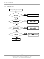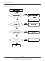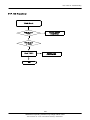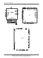
1
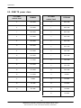
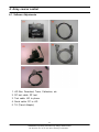
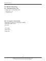
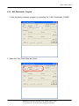
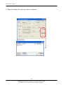
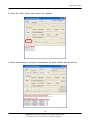
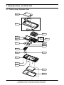
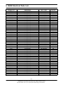
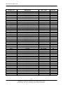
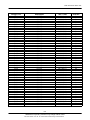
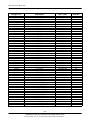
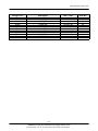
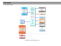
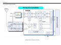
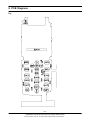
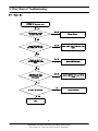
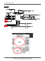
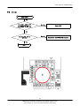
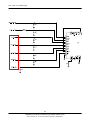
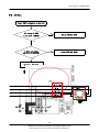
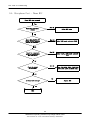
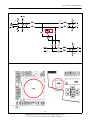
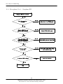
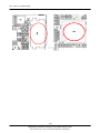
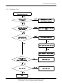
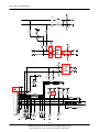
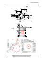
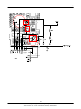
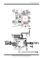
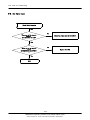
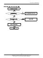
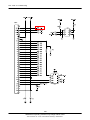
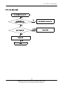
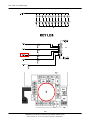
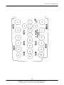
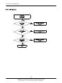
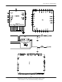
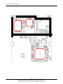
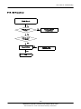
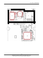
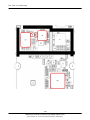
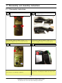
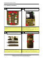
GSM TELEPHONE
SGH-C450
GSM TELEPHONE
CONTENTS
1.
Safety Precautions
2.
Specification
3.
Product Function
4.
Array course control
5.
Exploded View and Parts List
6.
MAIN Electrical Parts List
7.
Block Diagrams
8.
PCB Diagrams
9.
Flow Chart of Troubleshooting
10.
Reference data
11.
Disassembly and Assembly
Instructions
GSPN (Global Service Partner Network)
Country
North America
Latin America
CIS
Europe
China
Asia
Mideast & Africa
Web Site
service.samsungportal.com
latin.samsungportal.com
cis.samsungportal.com
europe.samsungportal.com
china.samsungportal.com
asia.samsungportal.com
mea.samsungportal.com
This Service Manual is a property of Samsung Electronics Co.,Ltd.
Any unauthorized use of Manual can be punished under applicable
International and/or domestic law.
ⓒ Samsung Electronics Co.,Ltd.
2007. 08 Rev.1.0
1. Safety Precautions
1-1. Repair Precaution
● Repair in Shield Box, during detailed tuning.
Take specially care of tuning or test, because the specification of cellular phone is sensitive for
surrounding interference(RF noise).
● Be careful to use a kind of magnetic object or tool, because performance of parts is damaged by the
influence of magnetic force.
● Surely use a standard screwdriver when you disassemble this product, otherwise screw will be worn
away.
● Use a thicken twisted wire when you measure level.
A thicken twisted wire has low resistance, therefore error of measurement is few.
● Repair after separate Test Pack and Set because for short danger (for example an
overcurrent and furious flames of parts etc) when you repair board in condition of
connecting Test Pack and tuning on.
● Take specially care of soldering, because Land of PCB is small and weak in heat.
● Surely tune on/off while using AC power plug, because a repair of battery charger is
dangerous when tuning ON/OFF PBA and Connector after disassembling charger
● Don't use as you pleases after change other material than replacement registered on SEC System.
Otherwise engineer in charge isn't charged with problem that you don't keep this rules.
1-1
SAMSUNG Proprietary-Contents may change without notice
This Document can not be used without Samsung's authorization
Safety Precautions
1-2. ESD(Electrostatically Sensitive Devices) Precaution
Several semiconductor may be damaged easily by static electricity. Such parts are called by ESD
(Electrostatically Sensitive Devices), for example IC,BGA chip etc. Read Precaution below.
You can prevent from ESD damage by static electricity.
● Remove static electricity remained your body before you touch semiconductor or parts with
semiconductor. There are ways that you touch an earthed place or wear static electricity
prevention string on wrist.
● Use earthed soldering steel when you connect or disconnect ESD.
● Use soldering removing tool to break static electricity. , otherwise ESD will be damaged by
static electricity.
● Don't unpack until you set up ESD on product. Because most of ESD are packed by box and
aluminum
plate to have conductive power,they are prevented from static electricity.
● You must maintain electric contact between ESD and place due to be set up until ESD is connected
completely to the proper place or a circuit board.
1-2
SAMSUNG Proprietary-Contents may change without notice
This Document can not be used without Samsung's authorization
2. Specification
2-1. GSM General Specification
EGSM 900
D CS 180 0
Fr eq. Band[ MHz]
Uplink/Downlink
880~91 5
925~96 0
1 710~17 85
1 805~18 80
ARFCN rang e
0~ 124 & 975~10 23
512~88 5
Tx/ Rx spacing
45MHz
95MHz
Mod. Bit rat e/
Bi t Pe rio d
27 0.833 kbps
3.692 us
27 0.833 kbps
3.692 us
T ime Slot Per iod/ Fra me
Period
576.9 us
4. 615ms
576.9 us
4. 615ms
Modu lation
0.3G MSK
0.3G M SK
M S P ow er
33 dBm ~ 5d Bm
30 dBm ~ 0d Bm
Power Cl ass
4
(max +33dBm)
1
(max +30dBm)
Sensitivity
-1 02dBm
-1 00dBm
T DM A M u x
8
8
Cell Ra dius
35Km
2Km
2-1
SAMSUNG Proprietary-Contents may change without notice
This Document can not be used without Samsung's authorization
Specification
2-2. GSM TX power class
TX Power
control level
TX Power
GSM900
control level
DCS1800
5
33±2 dBm
0
30±3 dBm
6
31±2 dBm
1
28±3 dBm
7
29±2 dBm
2
26±3 dBm
8
27±2 dBm
3
24±3 dBm
9
25±2 dBm
4
22±3 dBm
10
23±2 dBm
5
20±3 dBm
11
21±2 dBm
6
18±3 dBm
12
19±2 dBm
7
16±3 dBm
13
17±2 dBm
8
14±3 dBm
14
15±2 dBm
9
12±4 dBm
15
13±2 dBm
10
10±4 dBm
16
11±3 dBm
11
8±4dBm
17
9±3dBm
12
6±4 dBm
18
7±3 dBm
13
4±4 dBm
19
5±3 dBm
14
2±5 dBm
15
0±5 dBm
2-2
SAMSUNG Proprietary-Contents may change without notice
This Document can not be used without Samsung's authorization
3. Operation Instruction and Installation
Main Function
S20 Pin TA
No Java
No MMS
FM radio
WAP 2.0
10 Poly S/W MIDI
Dual band(900/1800MHz)
GPRS Class 10
VGA camera
3-1
SAMSUNG Proprietary-Contents may change without notice
This Document can not be used without Samsung's authorization
Operation Instruction and Installation
3-2
SAMSUNG Proprietary-Contents may change without notice
This Document can not be used without Samsung's authorization
4. Array course control
4-1. Software Adjustments
1.
2.
3.
4.
5.
JIG Box: Download, Trace, Calibration, etc
RF test cable: RF test
Test cable: JIG to phone
Serial cable: PC to JIG
TA (Travel Adaptor)
4-1
SAMSUNG Proprietary-Contents may change without notice
This Document can not be used without Samsung's authorization
Array course control
4-2. Software Downloading
4-2-1. Downloading Binary Files
• 2 binary files for downloading C450.
– C450XAGD3 .cla
– C450XAGD3.tfs
4-2-2. Pre-requsite for Downloading
• Downloader Program(C450 Downloader 2.0NEW)
• SGH-C450 Mobile Phone
• JIG BOX
• Test Cable
• Serial Cable
• Binary files
4-2
SAMSUNG Proprietary-Contents may change without notice
This Document can not be used without Samsung's authorization
Array course control
4-2-3. S/W Downloader Program
1. Load the binary download program by executing the “C450 Downloader 2.0NEW”.
2. Select the Port, Baud Rate and Mode.
4-3
SAMSUNG Proprietary-Contents may change without notice
This Document can not be used without Samsung's authorization
Array course control
3. Select the binary files what you want to download
4-4
SAMSUNG Proprietary-Contents may change without notice
This Document can not be used without Samsung's authorization
Array course control
4. Press the "Start" button and connect the Handset
5. When downloading is complete, automatically the small window was showed up..
4-5
SAMSUNG Proprietary-Contents may change without notice
This Document can not be used without Samsung's authorization
Array course control
4-6
SAMSUNG Proprietary-Contents may change without notice
This Document can not be used without Samsung's authorization
5. Exploded View and Parts List
5-1. Cellular phone Exploded View
QMW02
QSP05
QFR01
QRF03
QKP01
QLC01
QMI03
QMP01
QMI01
QME01
QSP01
QSH01
QCR17
QAN02
QCA01
QMO01
QRE01
QCR68
QRF01
QBA01
QBA00
5-1
SAMSUNG Proprietary-Contents may change without notice
This Document can not be used without Samsung's authorization
Exploded View and Parts List
5-2. Cellular phone Parts List
Design LOC
Description
SEC CODE
QAN02
INTENNA-SGHC420
GH42-01240A
QBA00
PMO COVER-BATTERY
GH72-41901B
QBA01
INNER BATTERY PACK-750MAH,BLK,
GH43-02483A
QCA01
CAMERA MODULE
GH59-04223A
QCR17
SCREW-MACHINE
6001-001460
QCR68
SCREW-TAPPING
6002-001399
QKP01
ASSY KEYPAD-(EU/BLK) V3
GH98-06072B
QLC01
LCD-LCD MODULE
GH07-01056A
QME01
DOME SHEET-DOME SHEET 22KEY(MA
GH59-04572A
QMO01
MOTOR DC
GH31-00296A
QMP01
PBA MAIN-SGHC450
GH92-03544A
QMW02
PCT COVER-WINDOW MAIN
GH72-41907B
QRE01
ASSY CASE-REAR
GH98-05044B
QRF01
TAPE-SHEET RF
GH74-32599B
QSH01
ASSY BRACKET-SHIELD CAN
GH98-05378A
QSP01
SPEAKER
3001-002100
QMI01
MICROPHONE-ASSY-SGHC420
GH30-00390A
AS-SCHS299 MIC RUBBER HOLDER
GH81-06644A
ASSY CASE-FRONT
GH98-05043B
QRF03
PMO COVER-EAR V2
GH72-42135B
QSP05
ASSY DECO-SPK GRILL
GH98-04853A
QMI03
QFR01
5-2
SAMSUNG Proprietary-Contents may change without notice
This Document can not be used without Samsung's authorization
Exploded View and Parts List
Description
SEC CODE
BAG PE
6902-000634
ADAPTOR-ATADS10EBE,BLK,EU
GH44-01702A
EARPHONE-AAEP405MBE,S20,BLK,EU
GH59-04874A
LABEL(P)-UNIT SEAL
GH68-00518B
LABEL(P)-IMEI
GH68-01335D
LABEL(R)-WATER SOAK
GH68-09361A
LABEL(R)-MAIN(EU)
GH68-15206A
MANUAL USERS-EU ROMANIAN
GH68-15253A
BOX-UNIT(EU)
GH69-05570B
TAPE INSU
GH74-13822A
TAPE INSU
GH74-28075A
MPR-VINYL BOHO WINDOW
GH74-31711A
VINYL-BOHO WINDOW MAIN TOP
GH74-32641A
5-3
SAMSUNG Proprietary-Contents may change without notice
This Document can not be used without Samsung's authorization
Exploded View and Parts List
5-4
SAMSUNG Proprietary-Contents may change without notice
This Document can not be used without Samsung's authorization
6. MAIN Electrical Parts List
Design LOC
Description
SEC Code
STATUS
BAT600
C100
C101
C103
C104
C105
C106
C107
C108
C109
C110
C112
C113
C115
C116
C118
C119
C120
C121
C122
C123
C124
C202
C203
C204
C205
C206
C207
C208
C209
C210
C211
C212
C213
C214
C216
C217
C218
C219
C220
C221
C300
C301
C302
C303
C304
C305
C306
C307
C308
C309
C310
C311
HEADER-BATTERY
C-CER,CHIP
INDUCTOR-SMD
C-CER,CHIP
C-CER,CHIP
C-CER,CHIP
C-CER,CHIP
C-CER,CHIP
C-CER,CHIP
C-CER,CHIP
C-CER,CHIP
C-CER,CHIP
C-CER,CHIP
C-CER,CHIP
C-CER,CHIP
C-CER,CHIP
C-CER,CHIP
C-CER,CHIP
C-CER,CHIP
C-CER,CHIP
C-CER,CHIP
C-CER,CHIP
C-CER,CHIP
C-CER,CHIP
C-CER,CHIP
C-CER,CHIP
C-CER,CHIP
C-CER,CHIP
C-CER,CHIP
C-CER,CHIP
C-CER,CHIP
C-CER,CHIP
C-CER,CHIP
C-CER,CHIP
C-CER,CHIP
C-CER,CHIP
C-CER,CHIP
C-CER,CHIP
C-CER,CHIP
C-CER,CHIP
C-CER,CHIP
C-CER,CHIP
C-CER,CHIP
C-CER,CHIP
C-CER,CHIP
C-CER,CHIP
C-CER,CHIP
C-CER,CHIP
C-CER,CHIP
C-CER,CHIP
C-CER,CHIP
C-CER,CHIP
C-CER,CHIP
3711-006228
2203-000854
2703-001726
2203-005050
2203-006048
2203-006361
2203-000812
2203-000812
2203-000812
2203-000489
2203-005482
2203-005482
2203-005234
2203-005234
2203-005288
2203-000254
2203-005288
2203-005482
2203-000278
2203-005050
2203-000278
2203-000679
2203-002709
2203-002709
2203-002709
2203-002709
2203-000254
2203-002709
2203-002709
2203-000254
2203-000254
2203-005482
2203-005482
2203-000854
2203-000679
2203-005482
2203-005481
2203-005481
2203-005482
2203-002709
2203-002709
2203-000278
2203-000330
2203-000812
2203-006824
2203-006824
2203-006257
2203-006257
2203-006257
2203-006257
2203-006257
2203-005482
2203-006257
SA
SA
SA
SA
SA
SA
SA
SA
SA
SA
SA
SA
SA
SA
SA
SA
SA
SA
SA
SA
SA
SA
SA
SA
SA
SA
SA
SA
SA
SA
SA
SA
SA
SA
SA
SA
SA
SA
SA
SA
SA
SA
SA
SA
SA
SA
SA
SA
SA
SA
SA
SA
SA
6-1
SAMSUNG Proprietary-Contents may change without notice
This Document can not be used without Samsung's authorization
Main Electrical Parts List
Design LOC
Description
SEC Code
STATUS
C312
C313
C314
C316
C317
C318
C327
C328
C329
C330
C400
C401
C402
C404
C405
C406
C407
C408
C410
C413
C415
C416
C417
C418
C419
C420
C421
C422
C423
C424
C425
C426
C427
C428
C429
C430
C501
C503
C504
C506
C507
C508
C509
C510
C511
C512
C513
C514
C515
C600
C601
C602
C603
C-CER,CHIP
C-CER,CHIP
C-CER,CHIP
C-CER,CHIP
C-CER,CHIP
C-CER,CHIP
C-CER,CHIP
C-CER,CHIP
C-CER,CHIP
C-CER,CHIP
C-CER,CHIP
C-CER,CHIP
C-CER,CHIP
C-CER,CHIP
C-CER,CHIP
C-CER,CHIP
C-CER,CHIP
C-CER,CHIP
C-CER,CHIP
C-CER,CHIP
C-CER,CHIP
C-CER,CHIP
C-CER,CHIP
C-CER,CHIP
C-CER,CHIP
C-CER,CHIP
C-CER,CHIP
C-CER,CHIP
C-CER,CHIP
C-CER,CHIP
C-CER,CHIP
C-CER,CHIP
C-CER,CHIP
C-CER,CHIP
C-CER,CHIP
C-CER,CHIP
C-CER,CHIP
C-CER,CHIP
C-CER,CHIP
C-CER,CHIP
C-CER,CHIP
C-CER,CHIP
C-CER,CHIP
C-CER,CHIP
C-CER,CHIP
C-CER,CHIP
C-CER,CHIP
C-CER,CHIP
C-CER,CHIP
C-CER,CHIP
C-NETWORK
C-NETWORK
C-NETWORK
2203-006348
2203-006681
2203-006348
2203-006562
2203-006825
2203-005482
2203-002709
2203-005482
2203-000812
2203-006824
2203-000679
2203-002709
2203-000425
2203-000812
2203-002709
2203-000679
2203-005482
2203-005482
2203-006048
2203-001153
2203-000233
2203-005481
2203-005481
2203-005482
2203-006137
2203-006137
2203-006324
2203-006562
2203-006562
2203-006562
2203-000995
2203-000995
2203-006824
2203-006824
2203-006562
2203-006562
2203-000425
2203-000233
2203-006824
2203-001153
2203-001153
2203-001153
2203-000233
2203-005482
2203-005482
2203-005482
2203-006562
2203-006562
2203-005482
2203-000311
2503-001053
2503-001053
2503-001053
SA
SA
SA
SA
SA
SA
SA
SA
SA
SA
SA
SA
SA
SA
SA
SA
SA
SA
SA
SA
SA
SA
SA
SA
SA
SA
SA
SA
SA
SA
SA
SA
SA
SA
SA
SA
SA
SA
SA
SA
SA
SA
SA
SA
SA
SA
SA
SA
SA
SA
SA
SA
SA
6-2
SAMSUNG Proprietary-Contents may change without notice
This Document can not be used without Samsung's authorization
Main Electrical Parts List
Design LOC
Description
SEC Code
STATUS
C604
C605
C606
C607
C608
C609
C610
C611
C612
C613
C614
C615
C616
C617
C618
C619
CN601
D300
D401
D402
D403
D404
D501
D502
D503
D504
D505
D506
D601
F100
F501
F601
IFC500
L101
L102
L103
L104
L105
L106
L107
L108
L109
L110
L301
L302
L401
L402
L403
L404
L405
L406
L407
L408
C-NETWORK
C-CER,CHIP
C-CER,CHIP
C-CER,CHIP
C-CER,CHIP
C-CER,CHIP
C-CER,CHIP
C-CER,CHIP
C-CER,CHIP
C-CER,CHIP
C-CER,CHIP
C-CER,CHIP
C-NETWORK
C-NETWORK
C-CER,CHIP
C-CER,CHIP
CONNECTOR-FPC/FFC/PIC
DIODE-ARRAY
DIODE-TVS
DIODE-TVS
DIODE-TVS
DIODE-TVS
DIODE-TVS
DIODE-TVS
DIODE-TVS
DIODE-TVS
DIODE-TVS
DIODE-ZENER
DIODE-TVS
FILTER-SAW
FILTER-EMI/ESD
FILTER-EMI SMD
SOCKET-INTERFACE
INDUCTOR-SMD
INDUCTOR-SMD
INDUCTOR-SMD
INDUCTOR-SMD
INDUCTOR-SMD
INDUCTOR-SMD
INDUCTOR-SMD
INDUCTOR-SMD
INDUCTOR-SMD
R-CHIP
INDUCTOR-SMD
INDUCTOR-SMD
BEAD-SMD
BEAD-SMD
BEAD-SMD
BEAD-SMD
BEAD-SMD
BEAD-SMD
INDUCTOR-SMD
INDUCTOR-SMD
2503-001053
2203-006562
2203-006562
2203-000386
2203-002709
2203-000386
2203-002709
2203-002709
2203-000386
2203-000386
2203-002709
2203-006562
2503-001053
2503-001053
2203-000995
2203-000995
3708-002222
0407-001002
0406-001254
0406-001254
0406-001223
0406-001223
0406-001231
0406-001231
0406-001231
0406-001231
0406-001197
0403-001547
0406-001150
2904-001731
2901-001349
2901-001329
3710-002499
2703-002203
2703-002700
2703-002313
2703-002313
2703-002313
2703-002558
2703-002199
2703-002267
2703-002597
2007-000171
2703-002309
2703-002309
3301-001729
3301-001729
3301-001729
3301-001729
3301-001729
3301-001729
2703-002313
2703-002313
SA
SA
SA
SA
SA
SA
SA
SA
SA
SA
SA
SA
SA
SA
SA
SA
SA
SA
SA
SA
SA
SA
SA
SA
SA
SA
SA
SA
SA
SA
SA
SA
SA
SA
SA
SA
SA
SA
SA
SA
SA
SA
SA
SA
SA
SA
SA
SA
SA
SA
SA
SA
SA
6-3
SAMSUNG Proprietary-Contents may change without notice
This Document can not be used without Samsung's authorization
Main Electrical Parts List
Design LOC
Description
SEC Code
STATUS
L409
L501
L502
L503
L504
L505
L506
L601
LED601
LED602
LED603
LED604
LED605
LED606
LED607
LED608
LED609
LED610
LED611
LED612
MEM201
OSC100
OSC300
PAM100
Q501
R101
R103
R108
R109
R110
R111
R112
R114
R115
R118
R119
R120
R201
R202
R203
R207
R208
R209
R210
R211
R212
R214
R215
R216
R217
R219
R221
R222
INDUCTOR-SMD
BEAD-SMD
BEAD-SMD
INDUCTOR-SMD
BEAD-SMD
BEAD-SMD
BEAD-SMD
BEAD-SMD
LED
LED
LED
LED
LED
LED
LED
LED
LED
LED
LED
LED
IC-MCP
CRYSTAL-SMD
CRYSTAL-SMD
IC-POWER AMP
FET-SILICON
R-CHIP
R-CHIP
R-CHIP
R-CHIP
R-CHIP
R-CHIP
R-CHIP
R-CHIP
R-CHIP
R-CHIP
R-CHIP
R-CHIP
R-CHIP
R-CHIP
R-CHIP
R-CHIP
R-CHIP
R-CHIP
R-CHIP
R-CHIP
R-CHIP
R-CHIP
R-CHIP
R-CHIP
R-CHIP
R-CHIP
R-CHIP
R-CHIP
2703-002201
3301-001729
3301-001729
2703-001513
3301-001729
3301-001729
3301-001729
3301-001729
0601-002199
0601-002199
0601-002199
0601-002199
0601-002199
0601-002199
0601-002199
0601-002199
0601-002199
0601-002199
0601-002199
0601-002199
1108-000059
2801-004455
2801-003856
1201-002490
0505-002088
2007-007092
2007-000143
2007-000143
2007-000143
2007-000143
2007-000143
2007-003001
2007-000932
2007-000932
2007-003001
2007-000932
2007-000932
2007-000162
2007-000171
2007-000162
2007-000171
2007-000162
2007-000162
2007-000174
2007-000171
2007-000162
2007-007107
2007-000159
2007-007142
2007-007107
2007-000162
2007-000162
2007-000162
SA
SA
SA
SA
SA
SA
SA
SA
SA
SA
SA
SA
SA
SA
SA
SA
SA
SA
SA
SA
SA
SA
SA
SA
SA
SA
SA
SA
SA
SA
SA
SA
SA
SA
SA
SA
SA
SA
SA
SA
SA
SA
SA
SA
SA
SA
SA
SA
SA
SA
SA
SA
SA
6-4
SAMSUNG Proprietary-Contents may change without notice
This Document can not be used without Samsung's authorization
Main Electrical Parts List
Design LOC
Description
SEC Code
STATUS
R223
R224
R225
R226
R228
R229
R233
R234
R301
R304
R305
R306
R307
R308
R309
R310
R311
R312
R402
R404
R405
R406
R407
R408
R409
R410
R411
R412
R413
R414
R415
R416
R417
R418
R419
R420
R421
R422
R423
R500
R501
R502
R504
R505
R507
R508
R509
R510
R511
R512
R517
R518
R519
R-CHIP
R-CHIP
R-CHIP
R-CHIP
R-CHIP
R-CHIP
R-CHIP
R-CHIP
R-CHIP
R-CHIP
R-CHIP
R-CHIP
R-CHIP
R-CHIP
R-CHIP
R-CHIP
R-CHIP
R-CHIP
R-CHIP
R-CHIP
R-CHIP
R-CHIP
R-CHIP
R-CHIP
R-CHIP
R-CHIP
R-CHIP
R-CHIP
R-CHIP
R-CHIP
R-CHIP
R-CHIP
R-CHIP
R-CHIP
R-CHIP
R-CHIP
R-CHIP
R-CHIP
R-CHIP
R-CHIP
R-CHIP
R-CHIP
R-CHIP
R-CHIP
R-CHIP
R-CHIP
R-CHIP
R-CHIP
R-CHIP
R-CHIP
R-CHIP
R-CHIP
R-CHIP
2007-000162
2007-007141
2007-000171
2007-000162
2007-000141
2007-000141
2007-000162
2007-000143
2007-007100
2007-002796
2007-007573
2007-007334
2007-009379
2007-000170
2007-000162
2007-001339
2007-000758
2007-000148
2007-000148
2007-000140
2007-000140
2007-002796
2007-002796
2007-000140
2007-000140
2007-000172
2007-000171
2007-000138
2007-000171
2007-000138
2007-000172
2007-000171
2007-000171
2007-000148
2007-000148
2007-000157
2007-000171
2007-000162
2007-000162
2007-007009
2007-007009
2007-000162
2007-007107
2007-001339
2007-000171
2007-000171
2007-007107
2007-000143
2007-000143
2007-000171
2007-000171
2007-007014
2007-001303
SA
SA
SA
SA
SA
SA
SA
SA
SA
SA
SA
SA
SA
SA
SA
SA
SA
SA
SA
SA
SA
SA
SA
SA
SA
SA
SA
SA
SA
SA
SA
SA
SA
SA
SA
SA
SA
SA
SA
SA
SA
SA
SA
SA
SA
SA
SA
SA
SA
SA
SA
SA
SA
6-5
SAMSUNG Proprietary-Contents may change without notice
This Document can not be used without Samsung's authorization
Main Electrical Parts List
Design LOC
Description
SEC Code
STATUS
R520
R523
R524
R525
R526
R527
R528
R529
R530
R531
R601
R602
R603
R605
R606
R607
R608
R609
R610
R611
R612
R613
R614
R615
R616
R617
R618
R619
R620
RFS100
SIM300
TA100
TA301
TA302
TA303
TA401
TA402
TH200
TR300
U100
U300
U302
U400
U401
U402
U404
U501
U502
U503
U601
U602
UCP200
VR300
R-CHIP
R-CHIP
R-CHIP
R-CHIP
R-CHIP
R-CHIP
R-CHIP
R-CHIP
R-CHIP
R-CHIP
R-CHIP
R-CHIP
R-CHIP
R-CHIP
R-CHIP
R-CHIP
R-CHIP
R-CHIP
R-CHIP
R-CHIP
R-CHIP
R-CHIP
R-CHIP
R-CHIP
R-CHIP
R-CHIP
R-CHIP
R-CHIP
R-CHIP
CONNECTOR-COAXIAL
CONNECTOR-CARD EDGE
C-TA,CHIP
C-TA,CHIP
C-TA,CHIP
C-TA,CHIP
C-TA,CHIP
C-TA,CHIP
THERMISTOR-NTC
TR-POWER
IC-TRANSCEIVER
IC-POWER SUPERVISOR
IC-POSI.FIXED REG.
IC-ANALOG SWITCH
IC-AUDIO AMP
IC-DC/DC CONVERTER
IC-TUNER
IC ASIC-SGHC420
IC-CMOS LOGIC
FET-SILICON
FET-SILICON
R-CHIP
IC-COMM. CONTROLLER
VARISTOR
2007-007014
2007-000162
2007-000140
2007-000162
2007-000172
2007-000172
2007-000172
2007-000172
2007-001339
2007-001339
2007-000162
2007-000140
2007-000171
2007-000171
2007-000171
2007-000171
2007-003004
2007-001288
2007-003030
2007-003030
2007-000174
2007-000174
2007-003004
2007-000174
2007-003030
2007-003030
2007-000174
2007-000162
2007-003030
3705-001358
3709-001400
2404-001496
2404-001381
2404-001381
2404-001381
2404-001424
2404-001240
1404-001221
0502-001116
1205-003278
1203-004550
1203-004338
1001-001362
1201-002492
1203-004765
1204-002700
GH13-00057A
0801-002237
0505-001469
0505-001469
2007-000162
1205-003192
1405-001082
SA
SA
SA
SA
SA
SA
SA
SA
SA
SA
SA
SA
SA
SA
SA
SA
SA
SA
SA
SA
SA
SA
SA
SA
SA
SA
SA
SA
SA
SA
SA
SA
SA
SA
SA
SA
SA
SA
SA
SA
SA
SA
SA
SA
SA
SA
SA
SA
SA
SA
SA
SA
SA
6-6
SAMSUNG Proprietary-Contents may change without notice
This Document can not be used without Samsung's authorization
Main Electrical Parts List
Design LOC
Description
SEC Code
STATUS
VR301
VR601
VR602
VR603
VR604
VR605
VR606
VR607
VR608
VR609
ZD100
ZD300
VARISTOR
VARISTOR
VARISTOR
VARISTOR
VARISTOR
VARISTOR
VARISTOR
VARISTOR
VARISTOR
VARISTOR
DIODE-TVS
DIODE-ZENER
1405-001082
1405-001082
1405-001082
1405-001082
1405-001082
1405-001082
1405-001082
1405-001082
1405-001082
1405-001121
0406-001267
0403-001340
SA
SA
SA
SA
SA
SA
SA
SA
SA
SA
SA
SA
6-7
SAMSUNG Proprietary-Contents may change without notice
This Document can not be used without Samsung's authorization
Main Electrical Parts List
6-8
SAMSUNG Proprietary-Contents may change without notice
This Document can not be used without Samsung's authorization
7. Block Diagrams
7-1. Main Block Diagram
7-1
SAMSUNG Proprietary-Contents may change without notice
This Document can not be used without Samsung's authorization
Block Diagrams
7-2. RF Solution Block Diagram
7-2
SAMSUNG Proprietary-Contents may change without notice
This Document can not be used without Samsung's authorization
8. PCB Diagrams
Top
8-1
SAMSUNG Proprietary-Contents may change without notice
This Document can not be used without Samsung's authorization
PCB Diagrams
Bottom
8-2
SAMSUNG Proprietary-Contents may change without notice
This Document can not be used without Samsung's authorization
9. Flow Chart of Troubleshooting
9-1. Power On
'POWER ON' does not work
Yes
Not OK
Check battery voltage
is higher than 3.3V
Change battery
OK
Not OK
Check VCC_SYN_2.8V
and VDD3_1.8V of U101
Solder PMIC, U101, C120 and C121
again
OK
Not OK
Check the pin 1 of
OSC100 produces clock
signal
Solder OSC100 again
OK
Not OK
Check the pin 7 of
U101 produces 13M
pulse signal
Solder OSC100, U101 and C118
again
OK
No
Is Power On working?
Repeat sequence
Yes
END
9-1
SAMSUNG Proprietary-Contents may change without notice
This Document can not be used without Samsung's authorization
Flow Chart of Troubleshooting
Power On
9-2
SAMSUNG Proprietary-Contents may change without notice
This Document can not be used without Samsung's authorization
Flow Chart of Troubleshooting
9-2. Initial
Initial Failure
Yes
Check VDD1, VDD3=1.8V,
VDD2=2.8V and
AVDD=2.6V of UCP 200
Not OK
Check U300
OK
Not OK
Check D_REF_13M of
UCP 200
Check U100 and POWER ON Sequence
OK
END
9-3
SAMSUNG Proprietary-Contents may change without notice
This Document can not be used without Samsung's authorization
Flow Chart of Troubleshooting
9-4
SAMSUNG Proprietary-Contents may change without notice
This Document can not be used without Samsung's authorization
Flow Chart of Troubleshooting
9-3. SIM Part
"Insert SIM" is displayed on the LCD
The voltage is 2.8V
No
at the pin#1 SIM300
Check UCP200, C419
Yes
Is there any signal
pin #2,3,4 of SIM300?
No
Check UCP 200, U300
Yes
Check the SIM Card
END
9-5
SAMSUNG Proprietary-Contents may change without notice
This Document can not be used without Samsung's authorization
Flow Chart of Troubleshooting
9-4. Microphone Part - Phone MIC
Phone MIC does not work
Yes
Not OK
Check the connection
of MIC
Solder MIC again
OK
Check MIC_BIAS_2.15V
( When UCP200 operates
and call is connected )
Not OK
Solder R325 again and check U300
OK
Not OK
Check the components
which are connected to
MIC_BIAS_2.15V
Solder TA401, R405, R406 and R407
again
OK
Not OK
Check the circuit
of MIC PART
Solder C401,C402, C404, C405, L401,
L402, L403, L404 and R402 again
OK
No
Is Phone MIC working?
Replace MIC
Yes
END
9-6
SAMSUNG Proprietary-Contents may change without notice
This Document can not be used without Samsung's authorization
Flow Chart of Troubleshooting
9-7
SAMSUNG Proprietary-Contents may change without notice
This Document can not be used without Samsung's authorization
Flow Chart of Troubleshooting
9-5. Microphone Part - Earphone MIC
Earphone MIC does not work
Yes
Not OK
Check the connection
of IFC500
Solder pin 3, 4 of IFC500 again
OK
Not OK
Check JACK IN is low
when ear jack is inserted.
Solder IFC500, R505 again
OK
Not OK
Check MIC_BIAS_2.15V
( When UCP200 operates
and call is connected )
Solder R325 again and check U300
OK
Not OK
Check the circuit
of EAR MIC
Solder L501, L502, C407, C408,
C413 and R418 again
OK
Is Earphone MIC working?
No
Repeat the sequence
Yes
END
9-8
SAMSUNG Proprietary-Contents may change without notice
This Document can not be used without Samsung's authorization
Flow Chart of Troubleshooting
9-9
SAMSUNG Proprietary-Contents may change without notice
This Document can not be used without Samsung's authorization
Flow Chart of Troubleshooting
9-10
SAMSUNG Proprietary-Contents may change without notice
This Document can not be used without Samsung's authorization
Flow Chart of Troubleshooting
9-6. Earphone Part
Earphone does not work
Yes
Not OK
Check the circuit
of IFC500
Solder pin 5,6,7 of IFC500
, L504, L505 and L506 again
OK
Not OK
Check the voltages of
R502, R504, R505 and
R530 are 2.8V
Solder R344, R346, R347 and R530
again
OK
Not OK
Check the circuit
R500, R501 and U401
Solder R500 and R501 again
No
OK
Check R410, R415, C217 and C218
No
Check UCP200 or Change UCP200
Is JACK_INT signal
LOW?
(When UCP200 operates)
No
Solder R505 again
Yes
Not OK
Solder F501 again
Check EAR SW
Ok
END
9-11
SAMSUNG Proprietary-Contents may change without notice
This Document can not be used without Samsung's authorization
Flow Chart of Troubleshooting
9-12
SAMSUNG Proprietary-Contents may change without notice
This Document can not be used without Samsung's authorization
Flow Chart of Troubleshooting
9-13
SAMSUNG Proprietary-Contents may change without notice
This Document can not be used without Samsung's authorization
Flow Chart of Troubleshooting
9-7. Charging Part
Abnormal charging operation
Yes
Not OK
Check DC jack
OK
Not OK
Check the 32 Pin and
33 Pin of U300
Replace the U300
OK
Not OK
Check TR300 (E,B,C)
Replace the TR300
OK
Not OK
Check R307
Solder R307 again or change a
battery
OK
END
9-14
SAMSUNG Proprietary-Contents may change without notice
This Document can not be used without Samsung's authorization
Flow Chart of Troubleshooting
9-15
SAMSUNG Proprietary-Contents may change without notice
This Document can not be used without Samsung's authorization
Flow Chart of Troubleshooting
9-8. Speaker Part
Speaker does not work
Yes
Not OK
Solder L407 and L408 again
Check L407 and L408
Not OK
OK
Replace the speaker
Not OK
Check Pin #15, #17 of
U401
Solder U401 again
OK
Not OK
Check R410 and R415
Solder R410 and R415 again or
replace U401
OK
Not OK
Replace UCP200
Check UCP200
OK
END
9-16
SAMSUNG Proprietary-Contents may change without notice
This Document can not be used without Samsung's authorization
Flow Chart of Troubleshooting
9-17
SAMSUNG Proprietary-Contents may change without notice
This Document can not be used without Samsung's authorization
Flow Chart of Troubleshooting
9-9. Key Data Input
Check Initial Operation
Yes
No
When one of the keys is
pushed,
is it displayed on LCD?
Check the Dome sheet & Key FPCB
Yes
No
When one of the keys is
pushed,
KEYSENSE(0)~(4),KYPD9~1
7
Replace the PBA
Yes
END
9-18
SAMSUNG Proprietary-Contents may change without notice
This Document can not be used without Samsung's authorization
Flow Chart of Troubleshooting
9-10. Back Light (for Color Main LCD)
Backlight does not work
Yes
No
Is BACKLIGHT set
AlwaysON in the Menu?
Set BACKLIGHT on Always ON
Yes
Check the outflow voltage
of U402(PIN 5) is equal to
3.7V
Not OK
Replace U402
OK
Replace the LCD Module
Yes
END
9-19
SAMSUNG Proprietary-Contents may change without notice
This Document can not be used without Samsung's authorization
Flow Chart of Troubleshooting
9-20
SAMSUNG Proprietary-Contents may change without notice
This Document can not be used without Samsung's authorization
Flow Chart of Troubleshooting
9-11. Key Back Light
key Backlight does not work
Yes
No
Is BACKLIGHT set
AlwaysON in the Menu?
Set BACKLIGHT on Always ON
Yes
Not OK
Replace U300
Check V_KEY_3.2V
OK
Replace LED
Yes
END
9-21
SAMSUNG Proprietary-Contents may change without notice
This Document can not be used without Samsung's authorization
Flow Chart of Troubleshooting
9-22
SAMSUNG Proprietary-Contents may change without notice
This Document can not be used without Samsung's authorization
Flow Chart of Troubleshooting
9-23
SAMSUNG Proprietary-Contents may change without notice
This Document can not be used without Samsung's authorization
Flow Chart of Troubleshooting
9-15. GSM Receiver
RX ON
RF INPUT=62CH
AMP=-50dBm
Yes
Check PAM100
pin 7(EGSMRX)
≥-65dBm
No
Resolder or Change
PAM100
No
Resolder or Change
F100
No
Resolder or Change
UCP200
Yes
Check U100
pin 17, 18 (EGSMRX)
≥-65dBm
>
Yes
Check UCP200
MOD_STANDBY=HIGH
PON_PA=LOW
BAND=LOW
Yes
END
9-24
SAMSUNG Proprietary-Contents may change without notice
This Document can not be used without Samsung's authorization
Flow Chart of Troubleshooting
9-25
SAMSUNG Proprietary-Contents may change without notice
This Document can not be used without Samsung's authorization
Flow Chart of Troubleshooting
9-26
SAMSUNG Proprietary-Contents may change without notice
This Document can not be used without Samsung's authorization
Flow Chart of Troubleshooting
9-15. GSM Transmitter
TX ON (5Level)
Yes
No
PAM100 Pin11
Resolder PAM100
(TX MODULE)
≥ 30dBm
Yes
PAM100 pin17
≥ 20dBm
Yes
Check UCP200
No
Resolder U100
(TRANSCEIVER)
Yes
END
9-27
SAMSUNG Proprietary-Contents may change without notice
This Document can not be used without Samsung's authorization
Flow Chart of Troubleshooting
9-28
SAMSUNG Proprietary-Contents may change without notice
This Document can not be used without Samsung's authorization
Flow Chart of Troubleshooting
9-29
SAMSUNG Proprietary-Contents may change without notice
This Document can not be used without Samsung's authorization
Flow Chart of Troubleshooting
9-16. DCS Receiver
RX ON
RF INPUT=698CH
AMP=-50dBm
Yes
Check PAM100
pin 15(DCSRX)
≥-65dBm
No
Resolder or Change
PAM100
No
Resolder or Change
F100
No
Resolder or Change
UCP200
Yes
Check U100
pin 15, 16 (DCSRX)
≥-65dBm
>
Yes
Check UCP200
MOD_STANDBY= "HIGH"
PON_PA= "LOW"
BAND= "HIGH"
Yes
END
9-30
SAMSUNG Proprietary-Contents may change without notice
This Document can not be used without Samsung's authorization
Flow Chart of Troubleshooting
9-31
SAMSUNG Proprietary-Contents may change without notice
This Document can not be used without Samsung's authorization
Flow Chart of Troubleshooting
9-32
SAMSUNG Proprietary-Contents may change without notice
This Document can not be used without Samsung's authorization
Flow Chart of Troubleshooting
9-17. DCS Transmitter
TX ON (5Level)
Resolder PAM100
(TX MODULE)
PAM100 Pin11
≥ 30dBm
PAM100 pin19
≥ 20dBm
Check UCP200
Resolder U100
(TRANSCEIVER)
END
9-33
SAMSUNG Proprietary-Contents may change without notice
This Document can not be used without Samsung's authorization
Flow Chart of Troubleshooting
9-34
SAMSUNG Proprietary-Contents may change without notice
This Document can not be used without Samsung's authorization
Flow Chart of Troubleshooting
9-35
SAMSUNG Proprietary-Contents may change without notice
This Document can not be used without Samsung's authorization
Flow Chart of Troubleshooting
9-36
SAMSUNG Proprietary-Contents may change without notice
This Document can not be used without Samsung's authorization
10. Reference data
Reference Abbreviate
― ARFCN : Absolute Radio Frequency Channel Number
― BER : Bit Error Rate
― BPSK: Binary Phase Shift Keying
― ESD : Electrostatically Sensitive Devices
― ETSI: European Telecommunications Standards Institute
― MS: Mobile Station
― QPSK: Quadrature Phase Shift Keying
― RF : Radio Frequency
― TDMA : Time Division Multiple Access
10-1
SAMSUNG Proprietary-Contents may change without notice
This Document can not be used without Samsung's authorization
Reference data
10-2
SAMSUNG Proprietary-Contents may change without notice
This Document can not be used without Samsung's authorization
11. Disassembly and Assembly Instructions
11-1. Disassembly Instructions
1
1) Remove 4 screws from a rear case REAR
2
Screw.
1) Be cautious
when you remove a screw. It is
possible to damage a case or to scratch the one.
3
1) Be cautious
when you remove a screw. It is
possible to damage a case or to scratch the one.
Detach a locker which holds a PBA.
1) Be careful for breaking a component.
2) Disassemble a rear case by using a
disassembly knife.
4
Detach a speaker by using a pincette.
1) Be careful for damaging a speaker wire and a LCD
wire.
11-1
SAMSUNG Proprietary-Contents may change without notice
This Document can not be used without Samsung's authorization
Disassembly and Assembly Instructions
11-2. Assembly Instructions
1
1) Put a Keypad to a front case.
2
1)Insert a speaker and a LCD to a front case.
2)Insert a MIC to a hole which is shown below.
1) The Keypad should be inserted accurately into a
front case.
1) Be careful for inserting a LCD. Dust may be
attached to the LCD screen.
2) Be cautious when inserting a speaker. There is a
possibility for disconnecting a wire.
3
1) After pulling an earjack cover, assemble a
rear case to a front case like this.
1) Be cautious
when you remove a screw. It is
possible to damage a case or to scratch the one.
4
1) Screw on a rear case with 4 screws.
1) Be cautious
when you remove a screw. It is
possible to damage a case or to scratch the one.
11-2
SAMSUNG Proprietary-Contents may change without notice
This Document can not be used without Samsung's authorization