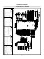
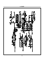
1
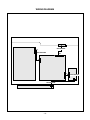
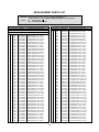
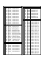
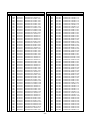
COLOR MONITOR
SERVICE MANUAL
CHASSIS NO. : CL-96
MODEL: LP2065
CAUTION
BEFORE SERVICING THE UNIT,
READ THE SAFETY PRECAUTIONS IN THIS MANUAL.
CONTENTS
SPECIFICATIONS ................................................... 2
PRECAUTIONS ....................................................... 4
TIMING CHART ....................................................... 8
DISASSEMBLY ....................................................... 9
BLOCK DIAGRAM ................................................. 10
DESCRIPTION OF BLOCK DIAGRAM....................11
ADJUSTMENT ...................................................... 13
SERVICE OSD ...................................................... 14
TROUBLESHOOTING GUIDE .............................. 15
WIRING DIAGRAM ................................................19
EXPLODED VIEW...................................................20
REPLACEMENT PARTS LIST ...............................22
SCHEMATIC DIAGRAM ......................................... 27
SPECIFICATIONS
1. LCD CHARACTERISTICS
Type
: TFT Color LCD Module
Active Display Area : 20.1inch diagonal
Pixel Pitch
: 0.255 (per one triad) x 0.255
Size
: 432(W) x 331.5(H) x 25.0(D)
Color Depth
:16.7M colors
Electrical Interface
: LVDS
Surface Treatment
: Hard Coating(3H), Anti-Glare
treatment of the front polarizer
Operating Mode
: Normally Black
Backlight Unit
: 6-CCFL
4. MAX. RESOLUTION
D-sub Analog
DVI Digital
5. POWER SUPPLY
5-1. Power Adaptor(Built-in Power)
Input
: AC 100~240V, 50/60Hz , 1.0A
5-2. Power Consumption
MODE
Right : +178 Typ
Bottom : -178 Typ
2-2. Luminance
: 250(min), 300(Typ)
2-3. Contrast Ratio
: 800 : 1 (Typ)
3. SIGNAL (Refer to the Timing Chart)
3-1. Sync Signal
• Type : Separate Sync, Digital, SOG
3-2. Video Input Signal
1) Type
2) Voltage Level
a) Color 0, 0
b) Color 7, 0
c) Color 15, 0
3) Input Impedance
3-3. Operating Frequency
Horizontal(Analog)
Horizontal(Digital)
Vertical
H/V SYNC VIDEO POWER CONSUMPTION LED COLOR
ACTIVE
less than 70 W
GREEN
STAND-BY
OFF/ON
OFF
less than 2 W
AMBER
SUSPEND
ON/OFF
OFF
less than 2 W
AMBER
DPMS OFF
OFF/OFF
OFF
less than 2 W
AMBER
POWER S/W OFF
-
-
less than 1W
OFF
POWER ON (NORMAL) ON/ON
2. OPTICAL CHARACTERISTICS
2-1. Viewing Angle by Contrast Ratio ≥ 10
Left : -178 Typ
Top : +178 Typ
: 1600 x 1200@75Hz
: 1600 x 1200@60Hz
6. ENVIRONMENT
6-1. Operating Temperature: 10°C~35°C
6-2. Relative Humidity
: 10%~80%
6-3. MTBF
: 50,000 HRS with 90%
Confidence level
Lamp Life
: 40,000 Hours(Min)
7. DIMENSIONS (with TILT/SWIVEL)
: R, G, B Analog
: 0~0.7 V
: 0 Vp-p
: 0.35 Vp-p
: 0.7 Vp-p
: 75 Ω
Width
Depth
Height
: 442 mm (17.40'')
: 277.5 mm (10.93'')
: 426 mm (16.77'')
8. WEIGHT (with TILT/SWIVEL)
Net. Weight
Gross Weight
: 30 ~ 94kHz
: 30 ~ 91.2kHz
: 48 ~ 85Hz
-2-
: 9.9 kg (21.83 lbs)
: 12.89 kg (28.42 lbs)
Signal Connector Pin Assignment
• DVI-I Connector (Digital/Analog)
1
9
17
8
16
24
Pin
1
2
3
4
5
6
7
8
9
10
11
12
13
14
15
Signal (DVI-I)
T. M. D. S. Data2T. M. D. S. Data2+
T. M. D. S. Data2/4 Shield
T. M. D. S. Data4T. M. D. S. Data4+
DDC Clock
DDC Data
Analog Vertical Sync.
T. M. D. S. Data1T. M. D. S. Data1+
T. M. D. S. Data1/3 Shield
T. M. D. S. Data3T. M. D. S. Data3+
+5V Power
Ground (return for +5V,
Pin
16
17
18
19
20
21
22
23
24
C1
C2
C3
C4
C5
Signal (DVI-I)
Hot Plug Detect
T. M. D. S. Data0T. M. D. S. Data0+
T. M. D. S. Data0/5 Shield
T. M. D. S. Data5T. M. D. S. Data5+
T. M. D. S. Clock Shield
T. M. D. S. Clock+
T. M. D. S. ClockAnalog Red
Analog Green
Analog Blue
Analog H. Sync.
Analog Ground
H. Sync. and V. Sync.)
T. M. D. S. (Transition Minimized Differential Signaling)
-3-
PRECAUTION
WARNING FOR THE SAFETY-RELATED COMPONENT.
WARNING
• There are some special components used in LCD
monitor that are important for safety. These parts are
marked on the schematic diagram and the
replacement parts list. It is essential that these critical
parts should be replaced with the manufacturer’s
specified parts to prevent electric shock, fire or other
hazard.
• Do not modify original design without obtaining written
permission from manufacturer or you will void the
original parts and labor guarantee.
BE CAREFUL ELECTRIC SHOCK !
• If you want to replace with the new backlight (CCFL) or
inverter circuit, must disconnect the AC adapter
because high voltage appears at inverter circuit about
650Vrms.
• Handle with care wires or connectors of the inverter
circuit. If the wires are pressed cause short and may
burn or take fire.
Leakage Current Hot Check Circuit
TAKE CARE DURING HANDLING THE LCD MODULE
WITH BACKLIGHT UNIT.
AC Volt-meter
• Must mount the module using mounting holes arranged
in four corners.
• Do not press on the panel, edge of the frame strongly
or electric shock as this will result in damage to the
screen.
• Do not scratch or press on the panel with any sharp
objects, such as pencil or pen as this may result in
damage to the panel.
• Protect the module from the ESD as it may damage the
electronic circuit (C-MOS).
• Make certain that treatment person’s body are
grounded through wrist band.
• Do not leave the module in high temperature and in
areas of high humidity for a long time.
• The module not be exposed to the direct sunlight.
• Avoid contact with water as it may a short circuit within
the module.
• If the surface of panel become dirty, please wipe it off
with a softmaterial. (Cleaning with a dirty or rough cloth
may damage the panel.)
CAUTION
Please use only a plastic screwdriver to protect yourself
from shock hazard during service operation.
-4-
Good Earth Ground
such as WATER PIPE,
CONDUIT etc.
To Instrument's
exposed
METALLIC PARTS
1.5 Kohm/10W
SERVICING PRECAUTIONS
CAUTION: Before servicing receivers covered by this
service manual and its supplements and addenda, read
and follow the SAFETY PRECAUTIONS on page 3 of this
publication.
NOTE: If unforeseen circumstances create conflict
between the following servicing precautions and any of the
safety precautions on page 3 of this publication, always
follow the safety precautions. Remember: Safety First.
General Servicing Precautions
1. Always unplug the receiver AC power cord from the AC
power source before;
a. Removing or reinstalling any component, circuit
board module or any other receiver assembly.
b. Disconnecting or reconnecting any receiver electrical
plug or other electrical connection.
c. Connecting a test substitute in parallel with an
electrolytic capacitor in the receiver.
CAUTION: A wrong part substitution or incorrect
polarity installation of electrolytic capacitors may
result in an explosion hazard.
d. Discharging the picture tube anode.
2. Test high voltage only by measuring it with an
appropriate high voltage meter or other voltage
measuring device (DVM, FETVOM, etc) equipped with
a suitable high voltage probe.
Do not test high voltage by "drawing an arc".
3. Discharge the picture tube anode only by (a) first
connecting one end of an insulated clip lead to the
degaussing or kine aquadag grounding system shield
at the point where the picture tube socket ground lead
is connected, and then (b) touch the other end of the
insulated clip lead to the picture tube anode button,
using an insulating handle to avoid personal contact
with high voltage.
4. Do not spray chemicals on or near this receiver or any
of its assemblies.
5. Unless specified otherwise in this service manual,
clean electrical contacts only by applying the following
mixture to the contacts with a pipe cleaner, cottontipped stick or comparable non-abrasive applicator;
10% (by volume) Acetone and 90% (by volume)
isopropyl alcohol (90%-99% strength)
CAUTION: This is a flammable mixture.
Unless specified otherwise in this service manual,
lubrication of contacts in not required.
6. Do not defeat any plug/socket B+ voltage interlocks
with which receivers covered by this service manual
might be equipped.
7. Do not apply AC power to this instrument and/or any of
its electrical assemblies unless all solid-state device
heat sinks are correctly installed.
8. Always connect the test receiver ground lead to the
receiver chassis ground before connecting the test
receiver positive lead.
Always remove the test receiver ground lead last.
9. Use with this receiver only the test fixtures specified in
this service manual.
CAUTION: Do not connect the test fixture ground strap
to any heat sink in this receiver.
Electrostatically Sensitive (ES) Devices
Some semiconductor (solid-state) devices can be
damaged easily by static electricity. Such components
commonly are called Electrostatically Sensitive (ES)
Devices. Examples of typical ES devices are integrated
circuits and some field-effect transistors and
semiconductor "chip" components. The following
techniques should be used to help reduce the incidence of
component damage caused by static by static electricity.
1. Immediately before handling any semiconductor
component or semiconductor-equipped assembly, drain
off any electrostatic charge on your body by touching a
known earth ground. Alternatively, obtain and wear a
commercially available discharging wrist strap device,
which should be removed to prevent potential shock
reasons prior to applying power to the unit under test.
2. After removing an electrical assembly equipped with
ES devices, place the assembly on a conductive
surface such as aluminum foil, to prevent electrostatic
charge buildup or exposure of the assembly.
3. Use only a grounded-tip soldering iron to solder or
unsolder ES devices.
4. Use only an anti-static type solder removal device.
Some solder removal devices not classified as "antistatic" can generate electrical charges sufficient to
damage ES devices.
5. Do not use freon-propelled chemicals. These can
generate electrical charges sufficient to damage ES
devices.
6. Do not remove a replacement ES device from its
protective package until immediately before you are
ready to install it. (Most replacement ES devices are
packaged with leads electrically shorted together by
conductive foam, aluminum foil or comparable
conductive material).
7. Immediately before removing the protective material
from the leads of a replacement ES device, touch the
protective material to the chassis or circuit assembly
into which the device will be installed.
CAUTION: Be sure no power is applied to the chassis
or circuit, and observe all other safety precautions.
8. Minimize bodily motions when handling unpackaged
replacement ES devices. (Otherwise harmless motion
such as the brushing together of your clothes fabric or
the lifting of your foot from a carpeted floor can
generate static electricity sufficient to damage an ES
device.)
-5-
General Soldering Guidelines
1. Use a grounded-tip, low-wattage soldering iron and
appropriate tip size and shape that will maintain tip
temperature within the range or 500。F to 600。F.
2. Use an appropriate gauge of RMA resin-core solder
composed of 60 parts tin/40 parts lead.
3. Keep the soldering iron tip clean and well tinned.
4. Thoroughly clean the surfaces to be soldered. Use a
mall wire-bristle (0.5 inch, or 1.25cm) brush with a
metal handle.
Do not use freon-propelled spray-on cleaners.
5. Use the following unsoldering technique
a. Allow the soldering iron tip to reach normal
temperature.
(500。F to 600。F)
b. Heat the component lead until the solder melts.
c. Quickly draw the melted solder with an anti-static,
suction-type solder removal device or with solder
braid.
CAUTION: Work quickly to avoid overheating the
circuitboard printed foil.
6. Use the following soldering technique.
a. Allow the soldering iron tip to reach a normal
temperature (500。F to 600。F)
b. First, hold the soldering iron tip and solder the strand
against the component lead until the solder melts.
c. Quickly move the soldering iron tip to the junction of
the component lead and the printed circuit foil, and
hold it there only until the solder flows onto and
around both the component lead and the foil.
CAUTION: Work quickly to avoid overheating the
circuit board printed foil.
d. Closely inspect the solder area and remove any
excess or splashed solder with a small wire-bristle
brush.
IC Remove/Replacement
Some chassis circuit boards have slotted holes (oblong)
through which the IC leads are inserted and then bent flat
against the circuit foil. When holes are the slotted type,
the following technique should be used to remove and
replace the IC. When working with boards using the
familiar round hole, use the standard technique as
outlined in paragraphs 5 and 6 above.
Removal
1. Desolder and straighten each IC lead in one operation
by gently prying up on the lead with the soldering iron
tip as the solder melts.
2. Draw away the melted solder with an anti-static
suction-type solder removal device (or with solder
braid) before removing the IC.
Replacement
1. Carefully insert the replacement IC in the circuit board.
2. Carefully bend each IC lead against the circuit foil pad
and solder it.
3. Clean the soldered areas with a small wire-bristle
brush. (It is not necessary to reapply acrylic coating to
the areas).
"Small-Signal" Discrete Transistor
Removal/Replacement
1. Remove the defective transistor by clipping its leads as
close as possible to the component body.
2. Bend into a "U" shape the end of each of three leads
remaining on the circuit board.
3. Bend into a "U" shape the replacement transistor leads.
4. Connect the replacement transistor leads to the
corresponding leads extending from the circuit board
and crimp the "U" with long nose pliers to insure metal
to metal contact then solder each connection.
Power Output, Transistor Device
Removal/Replacement
1. Heat and remove all solder from around the transistor
leads.
2. Remove the heat sink mounting screw (if so equipped).
3. Carefully remove the transistor from the heat sink of the
circuit board.
4. Insert new transistor in the circuit board.
5. Solder each transistor lead, and clip off excess lead.
6. Replace heat sink.
Diode Removal/Replacement
1. Remove defective diode by clipping its leads as close
as possible to diode body.
2. Bend the two remaining leads perpendicular y to the
circuit board.
3. Observing diode polarity, wrap each lead of the new
diode around the corresponding lead on the circuit
board.
4. Securely crimp each connection and solder it.
5. Inspect (on the circuit board copper side) the solder
joints of the two "original" leads. If they are not shiny,
reheat them and if necessary, apply additional solder.
Fuse and Conventional Resistor
Removal/Replacement
1. Clip each fuse or resistor lead at top of the circuit board
hollow stake.
2. Securely crimp the leads of replacement component
around notch at stake top.
3. Solder the connections.
CAUTION: Maintain original spacing between the
replaced component and adjacent components and the
circuit board to prevent excessive component
temperatures.
-6-
Circuit Board Foil Repair
Excessive heat applied to the copper foil of any printed
circuit board will weaken the adhesive that bonds the foil
to the circuit board causing the foil to separate from or
"lift-off" the board. The following guidelines and
procedures should be followed whenever this condition is
encountered.
At IC Connections
To repair a defective copper pattern at IC connections use
the following procedure to install a jumper wire on the
copper pattern side of the circuit board. (Use this
technique only on IC connections).
1. Carefully remove the damaged copper pattern with a
sharp knife. (Remove only as much copper as
absolutely necessary).
2. carefully scratch away the solder resist and acrylic
coating (if used) from the end of the remaining copper
pattern.
3. Bend a small "U" in one end of a small gauge jumper
wire and carefully crimp it around the IC pin. Solder the
IC connection.
4. Route the jumper wire along the path of the out-away
copper pattern and let it overlap the previously scraped
end of the good copper pattern. Solder the overlapped
area and clip off any excess jumper wire.
At Other Connections
Use the following technique to repair the defective copper
pattern at connections other than IC Pins. This technique
involves the installation of a jumper wire on the
component side of the circuit board.
1. Remove the defective copper pattern with a sharp
knife.
Remove at least 1/4 inch of copper, to ensure that a
hazardous condition will not exist if the jumper wire
opens.
2. Trace along the copper pattern from both sides of the
pattern break and locate the nearest component that is
directly connected to the affected copper pattern.
3. Connect insulated 20-gauge jumper wire from the lead
of the nearest component on one side of the pattern
break to the lead of the nearest component on the
other side.
Carefully crimp and solder the connections.
CAUTION: Be sure the insulated jumper wire is
dressed so the it does not touch components or sharp
edges.
-7-
TIMING CHART
VIDEO
A
E
D
B
SYNC
C
MODE
H/V
Sync
Polarity
Dot
Clock
1
H
V
H
V
H
V
H
V
H
V
H
V
H
V
H
V
H
V
H
V
H
V
H
V
H
V
H
V
H
V
H
V
H
V
H
V
+
+
+
+
+
+
+
+
+
+
+
+
+
+
+
+
+
+
+
+
+
28.35
2
3
4
5
6
7
8
9
10
11
12
13
14
15
16
17
18
25.175
31.5
36
40
56.25
57.285
65
78.75
94.5
100
92.94
108
108
135
157.5
162
202.5
Frequency
31.500 KHz
70.156 Hz
31.469KHz
59.940 Hz
37.50KHz
75.0 Hz
43.269KHz
85.008 Hz
37.879 KHz
60.317 Hz
53.670KHz
85.06 Hz
49.727 KHz
74.553 Hz
48.363 KHz
60.004 Hz
60.023 KHz
75.029 Hz
68.677 KHz
85 Hz
68.681 KHz
75.062 Hz
61.795KHz
65.950Hz
60.000 KHz
60.000 Hz
63.981 KHz
60.020 Hz
79.976 KHz
75.025 Hz
91.146 KHz
85.02 Hz
75 KHz
60 Hz
93.75 KHz
75 Hz
Total
Period
(E)
900
449
800
525
840
500
832
509
1056
628
1048
631
1152
667
1344
806
1312
800
1376
808
1456
915
1504
937
1800
1000
1688
1066
1688
1066
1728
1072
2160
1250
2160
1250
Total
Period
(E)
720
400
640
480
640
480
640
480
800
600
800
600
832
624
1024
768
1024
768
1024
768
1152
870
1152
900
1280
960
1280
1024
1280
1024
1280
1024
1600
1200
1600
1200
-8-
Video
Active
Time ( A )
180
49
160
45
200
20
192
29
256
28
248
31
320
43
320
38
288
32
352
40
304
45
352
37
520
40
408
42
408
42
448
48
560
50
560
50
Front
Porch
(C)
108
3
96
2
64
3
56
3
128
4
64
3
64
3
136
6
96
3
96
3
128
3
128
4
112
3
112
3
144
3
160
3
192
3
192
3
Sync
Duration
(D)
54
34
48
33
120
16
80
25
88
23
152
27
224
37
160
29
176
28
208
36
144
39
194
31
312
36
248
38
248
38
224
44
304
46
304
46
Back
Porch
(F)
18
12
16
10
16
1
56
1
40
1
32
1
32
3
24
3
16
1
48
1
32
3
30
2
96
1
48
1
16
1
64
1
64
1
64
1
Resolution
720 x 400
640 x 480
640 x 480
640 x 480
800 x 600
800x600
832 x 624
(MAC16")
1024 x 768
1024 x 768
1024 x 768
1152 x 870
(MAC 21)
1152x900
1280 x 960
1280 x1024
1280 x 1024
1280 X 1024
1600x1200
1600x1200
DISASSEMBLY
#1
#2
Like the picture move.
Remove the stand.
#3
#4
Remove the screws.
Remove the screws.
#6
#5
Disassemble back cover.
1. Pull the front cover upward.
2. Then, let the all latches are separated.
3. Put the front face down.
#8
#7
Remove the 4 screws from each side of metal
frame.
Pull out the usb pcb.
-9-
DVI-2
Analog-2
- 10 -
Filter
EEPROM
Digital-2
EEPROM
Analog-2
Switch
MC14066B
18V-LPL
Inverter(6Lamps)
12V
5V
Analog signal 1
Switch
MC14066B
Power
Digital 2
5V
Regulator
Regulator
Regulator
1.8V
3.3V
2.5V
Micom
DVI
Rx
DVI-1
Digital Signal
(TMDS)
Analog-1
Switch
PI3HDMI412
ADC
Digital 1
EEPROM
Digital-1
1.8V
PLL
Analog signal 1
Switch
MC14066B
EEPROM
Analog-1
3.3V
Real
Color
OSD
Scaling
USB 25H04
Up
stream
2.5V
DDR RAM
MST9251
EEPROM
2.5V
Down
stream
Down
stream
Vcc
18V-LPL
5V-AUO
LED
Key
Down
stream
Down
stream
USB
Menu
Down
Up
Auto
Power
LVDS
BLOCK DIAGRAM
Panel
DESCRIPTION OF BLOCK DIAGRAM
1. Video Controller Part & Display Data Transmitter Part.(MST9251A)
This part amplifies the level of video signal for the digital conversion and converts from the analog video signal to the
digital video signal using a pixel clock.
The pixel clock for each mode is generated by the PLL.
The range of the pixel clock is from 25MHz to 205MHz.
This part consists of the Scaler, DDR-RAM IC which stores program data, Reset IC.
The Scaler gets the video signal converted analog to digital, interpolates input to 1600 X 1200 resolution signal and
outputs 8-bit R, G, B signal to transmitter.
Especially pre-amp / ADC / Video controller/ Transmitter are merged to one chip 'MST9251A' by M-star.
This part transmit digital signal from the Scaler to the receiver of module.
2. Power Part.
This part consists of the 3.3V, 2.5V and 1.8V regulators to convert power which is provided 5V in Power board.
18V is provided for LCD panel .
Also, 5V is converted 3.3V, 2.5V and 1.8V by regulator. Converted power is provided for IC in the main board.
3. MICOM Part.
This part consists of EEPROM IC which stores control data the Micom.
The Micom distinguishes polarity and frequency of the H/V sync are supplied from signal cable.
The controlled data of each modes is stored in EEPROM.
- 11 -
LIPS Board Block Diagram
18V
50 ~ 60Hz
EMI
COMPONENTS
INPUT RECTIFIER
AND FILTER
HVDC
ENERGY
TRANSFER
100KHz
OUTPUT RECTIFIER
AND FILTER
5V
GND
LINE
100 ~ 240V
PWM CONTROL
CIRCUIT
PRIMARY
18V
SIGNAL
COLLECTON
PHOTO COUPLER
ISOLATION
SECONDARY
INVERTER CIRCUIT
High Voltage output
Operation description_LIPS
1. EMI components.
This part contains of EMI components to comply with global marketing EMI standards like FCC, VCCI CISPR, the
circuit included a line-filter, across line capacitor and of course the primary protection fuse.
2. Input rectifier and filter.
This part function is for transfer the input AC voltage to a DC voltage through a bridge rectifier and a bulk capacitor.
3. Energy Transfer.
This part function is for transfer the primary energy to secondary through a power transformer.
4. Output rectifier and filter.
This part function is to make a pulse width modulation control and to provide the driver signal to power switch, to
adjust the duty cycle during different AC input and output loading condition to achieve the dc output stabilized, and
also the over power protection is also monitor by this part.
5. Photo-Coupler isolation.
This part function is to feed back the DC output changing status through a photo transistor to primary controller to
achieve the stabilized DC output voltage.
6. Signal collection.
This part function is to collect the any change from the DC output and feed back to the primary through photo
transistor.
7. Inverter
The inverter converts from DC18V to AC 700V and operate back-light lamp of module.
- 12 -
ADJUSTMENT
Windows EDID V1.0 User Manual
2. EDID Read & Write
1) Run WinEDID.exe
Operating System: MS Windows 98, 2000, XP
Port Setup: Windows 98 => Don’t need setup
Windows 2000, XP => Need to Port Setup.
This program is available to LCD Monitor only.
1. Port Setup
a) Copy “UserPort.sys” file to
“c:\WINNT\system32\drivers” folder
b) Run Userport.exe
2) Edit Week of Manufacture, Year of Manufacture,
Serial Number
a) Input User Info Data
b) Click “Update” button
c) Click “ Write” button
c) Remove all default number
d) Add 300-3FF
e) Click Start button.
f) Click Exit button.
- 13 -
SERVICE OSD
1) Turn off the power switch at the front side of the display.
2) Wait for about 5 seconds and press MENU, MINUS and POWER switch with 1 second interval.
3) The SVC OSD menu contains additional menus that the User OSD menu as described below.
a) Exit
b) ADC CAL. : W/Balance and Automatically sets the gain and offset value.
c) Nvram Initial : EEPROM initialize.
d) AGING : Select Aging mode(on/off).
e) Module select : Select applied module.
f) EDID select : Select Analog/Digital EDID when Aging ON.
g) 9300K : Allows you to set the R/G/B-9300K value manually.
6500K : Allows you to set the R/G/B-6500K value manually.
Offset : Allows you to set the R/G/B-Offset value manually.
Gain : Allows you to set the R/G/B-Gain value manually.
A
9
IBM
Compatible PC
Video Signal
Generator
15
10
5
11
6
1
6
1
5
C
13
se
d
PARALLEL PORT
tu
2C
OFF
ON
F
AL
L
EL
No
RS
23
5V
14
PA
R
5V
Power inlet (required)
ON
R
220
WE
VG
CS
T
PO
S
MO
NI
TO
R
B
4.7K
OFF
74LS06
E ST Switch
B
F V-Sync On/Off Switch
(Switch must be ON.)
Figure 1. Cable Connection
- 14 -
4.7K
4.7K
5V
E
YN
A
Power Select Switch
(110V/220V)
Power LED
V-S
Control Line
C
1
25
74LS06
TROUBLESHOOTING GUIDE
1. NO POWER
NO POWER
(POWER INDICATOR OFF)
1
CHECK J303 VOLTAGE
PIN5, PIN6 (5V)?
CHECK POWER BOARD,
AND FIND OUT A SHORT
POINT AS OPENING
EACH POWER LINE
NO
YES
CHECK
U501 PIN 8
VOLTAGE (5V)?
NO
CHECK 5VS LINE
(OPEN CHECK)
NO PROBLEM
YES
CHECK KEY CONTROL
CONNECTOR ROUTINE
2
3
1
IS U401
PIN102 (3.3V)
PIN102 (2.5V)
VOLTAGE ?
NO
CHECK 2.5V AND 1.8V LINE
YES
4
1
CHECK U401 PIN 202
PULSE
NO
CHECK X-TAL
YES
CHECK U401
Waveforms
1
J303-#5,6 (5V)
2
U401-#102(3.3V)
3
- 15 -
U401-#102(2.5V)
4
U401-#202
2. NO RASTER (OSD IS NOT DISPLAYED) – LIPS
NO RASTER
(OSD IS NOT DISPLAYED)
J303
PIN5, 6
5V?
NO
CHECK LIPS
YES
J303 PIN 9
5V?
NO
CHECK MICOM INV
ON/OFF PORT.
YES
J303 PIN 10
5V?
NO
1. CONFIRM BRIGHTNESS
OSD CONTRL STATE.
2. CHECK MICOM DIM-ADJ
PORT
YES
CHECK
PULSE AS
CONTACTING SCOPE
PROBE TO CAUTION LABEL.
(CONTACT PROBE TO
CAUTION LABEL.
CAN YOU SEE PULSE
AT YOUR
SCOPE?
NO
LIPS
YES
REPLACE CCFL LAMP
IN THE LCD MODULE
- 16 -
3. NO RASTER (OSD IS NOT DISPLAYED) - MAIN
NO RASTER
(OSD IS NOT DISPLAYED)
U401
PIN102 (3.3V)
PIN102 (2.5V)
NO
CHECK U205 ~ U207
YES
U401
PIN 202, 203
14.318MHZ?
4
NO
1. CHECK PIN 202, 203
SOLDERING CONDITION
2. CHECK X401
3. TROUBLE IN U201
YES
U401
PIN18,36 IS 64KHz H-SYNC?
PIN19,37 IS 60Hz V-SYNC?
IS PULSE APPEARED
AT SIGNAL PINS?
AT MODE 15?
NO
YES
TROUBLE IN CABLE
OR LCD MODULE
Waveforms
4
U401-#202, 203
- 17 -
CHECK CONNECTION LINE
FROM DVI-I TO U401
4. TROUBLE IN DPM
TROUBLE IN DPM
5
CHECK
U401 PIN 18,19,36,37
SYNC PULSE?
NO
YES
TROUBLE IN U401
Waveforms
5
U401-#18,36 H-SYNC
5
U401-#19,37 V-SYNC
- 18 -
CHECK H/V SYNC LINE
WIRING DIAGRAM
6631900055A
11P
6631T20034M
30P
15P
6631T20034E
10P
6631900053B
- 19 -
050
010
020
060
070
080
090
100
100
110
030
120
130
040
140
EXPLODED VIEW
- 20 -
EXPLODED VIEW PARTS LIST
* Note: Safety mark
Ref. No.
Description
Part No.
010
30919L0006A
Cover Assembly, LH2065N H/PACKARD 30909L0004A HP
020
6304FLP325B
LCD,Module-TFT, LM201U05-SLA3 DRIVER 20.1INCH 1600X1200 300CD COLOR 72% 4/3 800 VS. 1 8MS GTG, 178/178, 6LAMP, IMPROVED GHOST & IMAGE STICKING OF LM201U05-SLA1 LG PH
030
3809900115A
Cover Assembly, LH2065N NON HP
040
3043900007D
Base Assembly, BASE LHP2065N CL96 NT LOCAL STAND_LHP2065N
050
68719ST865A
PCB Assembly,Sub, SUB T.T CL96 LH2065N KLUSEPT -
060
6709900008A
SMPS,AC/DC, FSP060-3PI01 110.0VTO230.0V 60W 50TO60HZ - 20.1INCH LCD
070
33139L2008A
Main Total Assembly, LH2065N H/PACKARD CL-96.
080
68719ST864A
PCB Assembly,Sub, SUB T.T CL96 LH2065N KLUSEPT -
090
48149K0019A
Plate, PRESS SPTE T0.3 USB SHIELD LH2065N HP
100
4814TKK264A
Plate, PRESS SECC T0.3 INVERTER LL180PL SHIELD
110
49519S0015A
Plate Assembly, FRAME HP
120
49509K0278A
Plate, FIX HP QUICK RELEASE
130
35519K0008A
Cover Assembly, LH2065N REAR 35509K0151A QUICK RELEASE
140
6410TEW010A
Power Cord, CEE,LP-34A&H05VV-FX3C,LS-60_1.87M_BLK LP-34A LS-60 1.87M - 250V 16A H05VV-F 3X0.75MM2 BLACK VDE SEMKO N LONGWELL COMPANY-For Europe
6410TSW003A
Power Cord, LP-23A+SAG18N<B10A&LS-13_1.87M_BLK LP-23A LS-13 1.87M - 250V 7.5A GFC-3R 3X0.75MM2 BLACK SAA N-For Australia
6410TJW005A
Power Cord, PSE,LP-54 & VTF18OXC70A & LS-13J_1.87M_BLK LP-54 LS-13J 1.87M - 125V 7A VCTF 3X0.75MM2 BLACK PSE N-For Japan
6410TUW008A
Power Cord, UL_CSA,LP-31 & SVT 18X3C, LS-13_1.87M_BLK LP-31 LS-13 1.87M - 125V 10A SVT 3XAWG18 BLACK UL CSA N-For U.S.A
- 21 -
REPLACEMENT PARTS LIST
CAUTION: BEFORE REPLACING ANY OF THESE COMPONENTS,
READ CAREFULLY THE SAFETY PRECAUTIONS IN THIS MANUAL.
* NOTE : S SAFETY Mark
AL ALTERNATIVE PARTS
*S
*AL LOC. NO.
PART NO.
DATE: 2006. 11. 20.
DESCRIPTION / SPECIFICATION
*S
MAIN BOARD
CAPACITORS
C202
C203
C204
C205
C206
C207
C208
C209
C210
C213
C214
C218
C220
C221
C223
C224
C226
C227
C228
C229
C236
C250
C251
C252
C301
C302
C303
C304
C305
C306
C308
C310
C311
C313
C314
C316
C318
C320
C321
C322
C323
C324
C325
C326
C327
C328
C329
C330
C331
C332
C333
C334
0CK103CK51A
JCE475EK638
0CK104CK56A
0CK103CK51A
0CK104CK56A
JCE477EF638
0CK103CK51A
0CK103CK51A
JCE107EH638
0CK104CK56A
0CK103CK51A
JCE227BF638
JCE107EF638
0CK105DK94A
0CK104CK56A
JCE107EF638
0CK103CK51A
JCE107EF638
0CK104CK56A
0CK103CK51A
0CK103CK51A
0CK103CK51A
0CK104CK56A
JCE227BF638
JCE107EH638
0CK104CK56A
JCE107EF638
0CK104CK56A
0CK103CK51A
0CK103CK51A
0CK103CK51A
0CK103CK51A
0CK105DK94A
0CK103CK51A
0CK103CK51A
0CC101CK41A
0CC680CK41A
0CK104CK56A
0CK104CK56A
0CK104CK56A
0CK104CK56A
0CK104CK56A
0CK104CK56A
0CK104CK56A
0CK104CK56A
0CK224CF56A
0CK474CH94A
0CK103CK51A
0CK103CK51A
0CK103CK51A
0CK103CK51A
0CK103CK51A
*AL LOC. NO.
C335
C336
C337
C338
C341
C343
C344
C349
C350
C351
C352
C353
C354
C355
C356
C357
C358
C359
C360
C361
C362
C363
C364
C365
C366
C367
C368
C369
C370
C371
C372
C373
C375
C376
C377
C380
C381
C401
C402
C403
C404
C405
C406
C407
C408
C409
C410
C411
C412
C414
C415
C416
C417
C418
0603B103K500CT 10nF 10% 50V
KMG5.0TP50VB4.7M 4.7uF 20% 5
0603B104K500CT 100nF 10% 50V
0603B103K500CT 10nF 10% 50V
0603B104K500CT 100nF 10% 50V
KMG5.0TP16VB470M 470uF 20% 1
0603B103K500CT 10nF 10% 50V
0603B103K500CT 10nF 10% 50V
KMG5.0TP25VB100M 100uF 20% 2
0603B104K500CT 100nF 10% 50V
0603B103K500CT 10nF 10% 50V
KME5.0TP16VB220M 220uF 20% 1
KMG5.0TP16VB100M 100uF 20% 1
0805F105Z500CT 1uF -20TO+80%
0603B104K500CT 100nF 10% 50V
KMG5.0TP16VB100M 100uF 20% 1
0603B103K500CT 10nF 10% 50V
KMG5.0TP16VB100M 100uF 20% 1
0603B104K500CT 100nF 10% 50V
0603B103K500CT 10nF 10% 50V
0603B103K500CT 10nF 10% 50V
0603B103K500CT 10nF 10% 50V
0603B104K500CT 100nF 10% 50V
KME5.0TP16VB220M 220uF 20% 1
KMG5.0TP25VB100M 100uF 20% 2
0603B104K500CT 100nF 10% 50V
KMG5.0TP16VB100M 100uF 20% 1
0603B104K500CT 100nF 10% 50V
0603B103K500CT 10nF 10% 50V
0603B103K500CT 10nF 10% 50V
0603B103K500CT 10nF 10% 50V
0603B103K500CT 10nF 10% 50V
0805F105Z500CT 1uF -20TO+80%
0603B103K500CT 10nF 10% 50V
0603B103K500CT 10nF 10% 50V
C1608C0G1H101JT 100pF 5% 50V
C1608C0G1H680JT 68pF 5% 50V
0603B104K500CT 100nF 10% 50V
0603B104K500CT 100nF 10% 50V
0603B104K500CT 100nF 10% 50V
0603B104K500CT 100nF 10% 50V
0603B104K500CT 100nF 10% 50V
0603B104K500CT 100nF 10% 50V
0603B104K500CT 100nF 10% 50V
0603B104K500CT 100nF 10% 50V
0603B224K160CT 220nF 10% 16V
0603F474Z250CT 470nF -20TO+8
0603B103K500CT 10nF 10% 50V
0603B103K500CT 10nF 10% 50V
0603B103K500CT 10nF 10% 50V
0603B103K500CT 10nF 10% 50V
0603B103K500CT 10nF 10% 50V
- 22 -
PART NO.
0CK103CK51A
0CK103CK51A
0CK104CK56A
0CK103CK51A
0CC680CK41A
0CC101CK41A
0CC101CK41A
0CK104CK56A
0CK224CF56A
0CK104CK56A
0CK104CK56A
0CK104CK56A
0CK104CK56A
0CK474CH94A
0CK104CK56A
0CK104CK56A
0CK104CK56A
0CK104CK56A
0CK103CK51A
0CK103CK51A
0CK103CK51A
0CK103CK51A
0CK103CK51A
0CK103CK51A
0CK103CK51A
0CK102CK56A
0CK103CK51A
0CC101CK41A
0CC101CK41A
0CC101CK41A
0CC680CK41A
0CC680CK41A
0CK104CK56A
0CK104CK56A
0CK104CK56A
0CK104CK56A
0CK104CK56A
0CK473CK56A
0CK473CK56A
0CK473CK56A
0CK473CK56A
0CK473CK56A
0CK473CK56A
0CK104CK56A
0CK104CK56A
0CK104CK56A
0CK104CK56A
0CK473CK56A
0CK473CK56A
0CC270CK41A
0CC270CK41A
0CK104CK56A
0CK104CK56A
0CK473CK56A
DATE: 2006. 11. 20.
DESCRIPTION / SPECIFICATION
0603B103K500CT 10nF 10% 50V
0603B103K500CT 10nF 10% 50V
0603B104K500CT 100nF 10% 50V
0603B103K500CT 10nF 10% 50V
C1608C0G1H680JT 68pF 5% 50V
C1608C0G1H101JT 100pF 5% 50V
C1608C0G1H101JT 100pF 5% 50V
0603B104K500CT 100nF 10% 50V
0603B224K160CT 220nF 10% 16V
0603B104K500CT 100nF 10% 50V
0603B104K500CT 100nF 10% 50V
0603B104K500CT 100nF 10% 50V
0603B104K500CT 100nF 10% 50V
0603F474Z250CT 470nF -20TO+8
0603B104K500CT 100nF 10% 50V
0603B104K500CT 100nF 10% 50V
0603B104K500CT 100nF 10% 50V
0603B104K500CT 100nF 10% 50V
0603B103K500CT 10nF 10% 50V
0603B103K500CT 10nF 10% 50V
0603B103K500CT 10nF 10% 50V
0603B103K500CT 10nF 10% 50V
0603B103K500CT 10nF 10% 50V
0603B103K500CT 10nF 10% 50V
0603B103K500CT 10nF 10% 50V
0603B102K500CT 1nF 10% 50V X
0603B103K500CT 10nF 10% 50V
C1608C0G1H101JT 100pF 5% 50V
C1608C0G1H101JT 100pF 5% 50V
C1608C0G1H101JT 100pF 5% 50V
C1608C0G1H680JT 68pF 5% 50V
C1608C0G1H680JT 68pF 5% 50V
0603B104K500CT 100nF 10% 50V
0603B104K500CT 100nF 10% 50V
0603B104K500CT 100nF 10% 50V
0603B104K500CT 100nF 10% 50V
0603B104K500CT 100nF 10% 50V
C1608X7R1H473KT 47nF 10% 50V
C1608X7R1H473KT 47nF 10% 50V
C1608X7R1H473KT 47nF 10% 50V
C1608X7R1H473KT 47nF 10% 50V
C1608X7R1H473KT 47nF 10% 50V
C1608X7R1H473KT 47nF 10% 50V
0603B104K500CT 100nF 10% 50V
0603B104K500CT 100nF 10% 50V
0603B104K500CT 100nF 10% 50V
0603B104K500CT 100nF 10% 50V
C1608X7R1H473KT 47nF 10% 50V
C1608X7R1H473KT 47nF 10% 50V
C1608C0G1H270JT 27pF 5% 50V
C1608C0G1H270JT 27pF 5% 50V
0603B104K500CT 100nF 10% 50V
0603B104K500CT 100nF 10% 50V
C1608X7R1H473KT 47nF 10% 50V
*S
*AL LOC. NO.
C419
C420
C421
C422
C423
C428
C429
C430
C431
C433
C440
C441
C450
C451
C452
C453
C456
C457
C458
C459
C460
C461
C462
C464
C470
C471
C472
C473
C474
C475
C476
C477
C478
C479
C480
C481
C485
C486
C487
C490
C491
C492
C495
C496
C497
C498
C500
C501
C502
C503
C505
C506
C512
C513
C516
C604
C605
C606
C609
C610
C611
C612
PART NO.
0CK473CK56A
0CC100CK41A
0CC100CK41A
0CC100CK41A
0CK104CK56A
0CK104CK56A
0CK104CK56A
0CK104CK56A
0CK104CK56A
0CK104CK56A
0CK103CK51A
0CK104CK56A
0CK473CK56A
0CK473CK56A
0CK473CK56A
0CK473CK56A
0CK473CK56A
0CK473CK56A
0CK102CK56A
0CK473CK56A
0CK473CK56A
0CK473CK56A
0CK473CK56A
0CK104CK56A
0CK473CK56A
0CK473CK56A
0CK473CK56A
0CK473CK56A
0CK473CK56A
0CK473CK56A
0CK473CK56A
0CK473CK56A
0CK473CK56A
0CK473CK56A
0CK473CK56A
0CK104CK56A
0CC100CK41A
0CC100CK41A
0CC100CK41A
0CK473CK56A
0CK473CK56A
0CK473CK56A
0CK473CK56A
0CK473CK56A
0CK473CK56A
0CK102CK56A
0CK104CK56A
JCE106EK638
0CC101CK41A
0CC101CK41A
0CC680CK41A
0CC680CK41A
0CC330CK41A
0CC330CK41A
0CK104CK56A
0CK105CD56A
0CK102CK56A
0CK103CK51A
JCE106EK638
0CK103CK51A
0CK105CD56A
0CC360CK41A
DATE: 2006. 11. 20.
DESCRIPTION / SPECIFICATION
*S
C1608X7R1H473KT 47nF 10% 50V
C1608C0G1H100JT 10pF 5% 50V
C1608C0G1H100JT 10pF 5% 50V
C1608C0G1H100JT 10pF 5% 50V
0603B104K500CT 100nF 10% 50V
0603B104K500CT 100nF 10% 50V
0603B104K500CT 100nF 10% 50V
0603B104K500CT 100nF 10% 50V
0603B104K500CT 100nF 10% 50V
0603B104K500CT 100nF 10% 50V
0603B103K500CT 10nF 10% 50V
0603B104K500CT 100nF 10% 50V
C1608X7R1H473KT 47nF 10% 50V
C1608X7R1H473KT 47nF 10% 50V
C1608X7R1H473KT 47nF 10% 50V
C1608X7R1H473KT 47nF 10% 50V
C1608X7R1H473KT 47nF 10% 50V
C1608X7R1H473KT 47nF 10% 50V
0603B102K500CT 1nF 10% 50V X
C1608X7R1H473KT 47nF 10% 50V
C1608X7R1H473KT 47nF 10% 50V
C1608X7R1H473KT 47nF 10% 50V
C1608X7R1H473KT 47nF 10% 50V
0603B104K500CT 100nF 10% 50V
C1608X7R1H473KT 47nF 10% 50V
C1608X7R1H473KT 47nF 10% 50V
C1608X7R1H473KT 47nF 10% 50V
C1608X7R1H473KT 47nF 10% 50V
C1608X7R1H473KT 47nF 10% 50V
C1608X7R1H473KT 47nF 10% 50V
C1608X7R1H473KT 47nF 10% 50V
C1608X7R1H473KT 47nF 10% 50V
C1608X7R1H473KT 47nF 10% 50V
C1608X7R1H473KT 47nF 10% 50V
C1608X7R1H473KT 47nF 10% 50V
0603B104K500CT 100nF 10% 50V
C1608C0G1H100JT 10pF 5% 50V
C1608C0G1H100JT 10pF 5% 50V
C1608C0G1H100JT 10pF 5% 50V
C1608X7R1H473KT 47nF 10% 50V
C1608X7R1H473KT 47nF 10% 50V
C1608X7R1H473KT 47nF 10% 50V
C1608X7R1H473KT 47nF 10% 50V
C1608X7R1H473KT 47nF 10% 50V
C1608X7R1H473KT 47nF 10% 50V
0603B102K500CT 1nF 10% 50V X
0603B104K500CT 100nF 10% 50V
KMG5.0TP50VB10M 10uF 20% 50V
C1608C0G1H101JT 100pF 5% 50V
C1608C0G1H101JT 100pF 5% 50V
C1608C0G1H680JT 68pF 5% 50V
C1608C0G1H680JT 68pF 5% 50V
C1608C0G1H330JT 33pF 5% 50V
C1608C0G1H330JT 33pF 5% 50V
0603B104K500CT 100nF 10% 50V
C1608X7R1A105KT 1uF 10% 10V
0603B102K500CT 1nF 10% 50V X
0603B103K500CT 10nF 10% 50V
KMG5.0TP50VB10M 10uF 20% 50V
0603B103K500CT 10nF 10% 50V
C1608X7R1A105KT 1uF 10% 10V
C1608C0G1H360JT 36pF 5% 50V
*AL LOC. NO.
C613
C614
C615
C616
C618
C619
C620
C621
C622
C624
C625
C626
C627
C628
C629
C630
C631
C632
C633
C634
C635
C636
C637
C638
PART NO.
DATE: 2006. 11. 20.
DESCRIPTION / SPECIFICATION
0CC360CK41A
0CK104CK56A
0CK104CK56A
0CK103CK51A
0CK104CK56A
0CK104CK56A
JCE106EK638
0CK475CC94A
JCE227BF638
0CK104CK56A
0CK104CK56A
0CK104CK56A
0CK104CK56A
0CK104CK56A
0CK104CK56A
0CK104CK56A
JCE107EF638
0CK104CK56A
0CK472CK51A
JCE107EF638
0CK104CK56A
0CK104CK56A
0CK105CD56A
0CK105CD56A
C1608C0G1H360JT 36pF 5% 50V
0603B104K500CT 100nF 10% 50V
0603B104K500CT 100nF 10% 50V
0603B103K500CT 10nF 10% 50V
0603B104K500CT 100nF 10% 50V
0603B104K500CT 100nF 10% 50V
KMG5.0TP50VB10M 10uF 20% 50V
C1608Y5V0J475ZT 4.7uF -20TO+
KME5.0TP16VB220M 220uF 20% 1
0603B104K500CT 100nF 10% 50V
0603B104K500CT 100nF 10% 50V
0603B104K500CT 100nF 10% 50V
0603B104K500CT 100nF 10% 50V
0603B104K500CT 100nF 10% 50V
0603B104K500CT 100nF 10% 50V
0603B104K500CT 100nF 10% 50V
KMG5.0TP16VB100M 100uF 20% 1
0603B104K500CT 100nF 10% 50V
C1608Y5P1H472KT 4.7nF 10% 50
KMG5.0TP16VB100M 100uF 20% 1
0603B104K500CT 100nF 10% 50V
0603B104K500CT 100nF 10% 50V
C1608X7R1A105KT 1uF 10% 10V
C1608X7R1A105KT 1uF 10% 10V
0DD184009AA
0DS226009AA
0DS226009AA
0DS226009AA
0DS226009AA
0DS226009AA
0DS226009AA
0DS226009AA
0DS226009AA
0DS226009AA
0DS226009AA
0DS226009AA
0DSON00138A
0DSON00138A
0DSON00138A
0DS226009AA
0DS226009AA
0DS226009AA
0DS226009AA
0DS226009AA
0DS226009AA
0DS226009AA
0DS226009AA
0DS226009AA
0DS226009AA
0DS226009AA
0DD184009AA
0DSON00138A
0DS226009AA
0DS226009AA
0DS226009AA
0DS226009AA
0DS226009AA
0DS226009AA
0IPRP00682A
KDS184 KDS184 TP KEC - 85V KDS226 1.2V 85V 300MA 2A 4NS
KDS226 1.2V 85V 300MA 2A 4NS
KDS226 1.2V 85V 300MA 2A 4NS
KDS226 1.2V 85V 300MA 2A 4NS
KDS226 1.2V 85V 300MA 2A 4NS
KDS226 1.2V 85V 300MA 2A 4NS
KDS226 1.2V 85V 300MA 2A 4NS
KDS226 1.2V 85V 300MA 2A 4NS
KDS226 1.2V 85V 300MA 2A 4NS
KDS226 1.2V 85V 300MA 2A 4NS
KDS226 1.2V 85V 300MA 2A 4NS
MMBD301LT1G 600MV 30V - - 1.
MMBD301LT1G 600MV 30V - - 1.
MMBD301LT1G 600MV 30V - - 1.
KDS226 1.2V 85V 300MA 2A 4NS
KDS226 1.2V 85V 300MA 2A 4NS
KDS226 1.2V 85V 300MA 2A 4NS
KDS226 1.2V 85V 300MA 2A 4NS
KDS226 1.2V 85V 300MA 2A 4NS
KDS226 1.2V 85V 300MA 2A 4NS
KDS226 1.2V 85V 300MA 2A 4NS
KDS226 1.2V 85V 300MA 2A 4NS
KDS226 1.2V 85V 300MA 2A 4NS
KDS226 1.2V 85V 300MA 2A 4NS
KDS226 1.2V 85V 300MA 2A 4NS
KDS184 KDS184 TP KEC - 85V MMBD301LT1G 600MV 30V - - 1.
KDS226 1.2V 85V 300MA 2A 4NS
KDS226 1.2V 85V 300MA 2A 4NS
KDS226 1.2V 85V 300MA 2A 4NS
KDS226 1.2V 85V 300MA 2A 4NS
KDS226 1.2V 85V 300MA 2A 4NS
KDS226 1.2V 85V 300MA 2A 4NS
ICP-N70 50V 0 0V 2.5A 0W DIP
DIODEs
D304
D317
D318
D319
D320
D321
D322
D323
D324
D325
D326
D327
D332
D334
D335
D340
D341
D342
D343
D344
D345
D346
D347
D348
D349
D350
D355
D356
D601
D602
D603
D604
D605
D606
F201
- 23 -
*S
*AL LOC. NO.
PART NO.
DATE: 2006. 11. 20.
DESCRIPTION / SPECIFICATION
*S
*AL LOC. NO.
PART NO.
DATE: 2006. 11. 20.
DESCRIPTION / SPECIFICATION
TRANSISTOR
ZD301
ZD302
ZD303
ZD304
ZD305
ZD309
ZD315
ZD316
ZD317
ZD318
ZD319
ZD330
ZD331
ZD332
ZD333
ZD334
ZD337
ZD338
ZD339
ZD601
ZD602
0DZ560009DA
0DZ560009DA
0DZ560009DA
0DZ560009DA
0DZ560009DA
0DZ560009DA
0DZ560009DA
0DZ560009DA
0DZ560009DA
0DZ560009DA
0DZ560009DA
0DZ560009DA
0DZ560009DA
0DZ560009DA
0DZ560009DA
0DZ560009DA
0DZ560009DA
0DZ560009DA
0DZ560009DA
0DZ560009DA
0DZ560009DA
UDZS5.6B 5.6V 5.49TO5.73V 60
UDZS5.6B 5.6V 5.49TO5.73V 60
UDZS5.6B 5.6V 5.49TO5.73V 60
UDZS5.6B 5.6V 5.49TO5.73V 60
UDZS5.6B 5.6V 5.49TO5.73V 60
UDZS5.6B 5.6V 5.49TO5.73V 60
UDZS5.6B 5.6V 5.49TO5.73V 60
UDZS5.6B 5.6V 5.49TO5.73V 60
UDZS5.6B 5.6V 5.49TO5.73V 60
UDZS5.6B 5.6V 5.49TO5.73V 60
UDZS5.6B 5.6V 5.49TO5.73V 60
UDZS5.6B 5.6V 5.49TO5.73V 60
UDZS5.6B 5.6V 5.49TO5.73V 60
UDZS5.6B 5.6V 5.49TO5.73V 60
UDZS5.6B 5.6V 5.49TO5.73V 60
UDZS5.6B 5.6V 5.49TO5.73V 60
UDZS5.6B 5.6V 5.49TO5.73V 60
UDZS5.6B 5.6V 5.49TO5.73V 60
UDZS5.6B 5.6V 5.49TO5.73V 60
UDZS5.6B 5.6V 5.49TO5.73V 60
UDZS5.6B 5.6V 5.49TO5.73V 60
Q503
U205
U206
U207
U208
U303
U304
U330
U331
U332
U333
U334
U335
U401
U402
U501
U502
U603
U604
U605
U606
0IKE704200H
0IPMGFA003E
0IPMGSG016A
0IRH033200A
0IPMG00028A
0IMMR00014A
0IMMR00014A
0IMMR00014A
0IMMR00014A
0ISTL00031A
0ISTL00031A
0ISTL00031A
0IPRP00651A
0IPRP00575B
0IMMRHY051B
0IZZ9H0082A
0IMMRSG036B
0ITI204200B
0ITI204200B
0IPRP00016A
0IPMGFA003G
KIA7042AP -0.3TO15V 4.2V 400
FAN1086-1.5A 4TO7V 2.5V - SO
LD1086D2T18TR 3.4TO30V 1.8V
BA033FP-E2 4.3TO25V 3.3V 1W
AZ1117H-1.5TRE1 3TO10V 1.5V
M24C02-RMN6TP 2KBIT 256X8BIT
M24C02-RMN6TP 2KBIT 256X8BIT
M24C02-RMN6TP 2KBIT 256X8BIT
M24C02-RMN6TP 2KBIT 256X8BIT
MC74HC4066ADR2G MC74HC4066AD
MC74HC4066ADR2G MC74HC4066AD
MC74HC4066ADR2G MC74HC4066AD
PI3HDMI412ZHE 1.5TO2V - - 50
"MST9251A-LF-205 3VTO3.6V,2.2"
HY5DU283222AQP-4 128MBIT 1MX
MTV412PMV MTV412PMV128 MYSON
M24C16-WMN6TP 16KBIT 2KX8BIT
"TPS2042ADRG4,LF 2.7TO5.5V 20"
"TPS2042ADRG4,LF 2.7TO5.5V 20"
USB2504-JT 2.97TO3.63V 1.62T
FAN1117AS33X 4.8TO10.3V 3.3V
6210TCE001G
6210TCE001G
6200J00005E
6200J00005E
6200J00005E
6200J00005E
6200J00005E
6200J00005E
6210TCE001S
6210TCE001Z
6210TCE001Z
HH-1M3216-501JT 500OHM 3.2X1
HH-1M3216-501JT 500OHM 3.2X1
HH-1M2012-601JT 600OHM 2X1.2
HH-1M2012-601JT 600OHM 2X1.2
HH-1M2012-601JT 600OHM 2X1.2
HH-1M2012-601JT 600OHM 2X1.2
HH-1M2012-601JT 600OHM 2X1.2
HH-1M2012-601JT 600OHM 2X1.2
HU-1M2012-121 120OHM 2X1.25X
HH-1M2012-600JT 60OHM 2X1.25
HH-1M2012-600JT 60OHM 2X1.25
Q201
Q202
Q301
Q302
Q305
Q306
Q320
Q321
Q322
Q323
Q324
Q502
Q506
KST3904 NPN 6V 60V 40V 200MA
KST3904 NPN 6V 60V 40V 200MA
KST3906-MTF PNP -5V -40V -40
KST3906-MTF PNP -5V -40V -40
KST3904 NPN 6V 60V 40V 200MA
KST3904 NPN 6V 60V 40V 200MA
KST3904 NPN 6V 60V 40V 200MA
KST3904 NPN 6V 60V 40V 200MA
KSC1623-Y(MTF) NPN 5V 60V 50
KSC1623-Y(MTF) NPN 5V 60V 50
KSC1623-Y(MTF) NPN 5V 60V 50
KST3904 NPN 6V 60V 40V 200MA
KST3904 NPN 6V 60V 40V 200MA
RESISTORs
R201
R202
R203
R204
R205
R206
R207
R208
R209
R212
R222
R223
R224
R225
R227
R245
R3001
R3002
R3003
R3004
R3005
R3006
R3007
R3008
R3009
R301
R3010
R3011
R3012
R3013
R3014
R3015
R3016
R3017
R3018
R3019
R302
R3020
R3022
R3023
R303
R3030
R3031
R3032
R3033
ICs
FILTERs
L201
L202
L402
L403
L405
L406
L407
L409
L601
L604
L605
0TR390409AE
0TR390409AE
0TR390609FA
0TR390609FA
0TR390409AE
0TR390409AE
0TR390409AE
0TR390409AE
0TR162309CA
0TR162309CA
0TR162309CA
0TR390409AE
0TR390409AE
- 24 -
0RH4701D622
0RH4701D622
0RH4701D622
0RH4701D622
0RH1002D622
0RX0221K668
0RX0331K668
0RJ2202D677
0RX0331K668
0RJ5600D677
0RJ1000D677
0RJ1002D677
0RJ1002D677
0RJ4700D677
0RX0331K668
0RH0000D622
0RJ0682D677
0RJ4701D677
0RJ2000D677
0RJ2000D677
0RJ2000D677
0RJ2000D677
0RJ2000D677
0RJ2000D677
0RJ2000D677
0RJ0102D677
0RJ2000D677
0RJ1501D677
0RJ2000D677
0RJ2000D677
0RJ2000D677
0RJ2000D677
0RJ2000D677
0RJ2000D677
0RJ2000D677
0RJ2000D677
0RJ0102D677
0RJ0222D677
0RJ0222D677
0RJ1200D677
0RJ0102D677
0RJ1000D677
0RJ1000D677
0RJ0000D677
0RJ0000D677
MCR10EZHJ472 4.7KOHM 5% 1/8W
MCR10EZHJ472 4.7KOHM 5% 1/8W
MCR10EZHJ472 4.7KOHM 5% 1/8W
MCR10EZHJ472 4.7KOHM 5% 1/8W
MCR10EZHJ103 10KOHM 5% 1/8W
RSD02F4J2R20 2.2OHM 5% 2W 12
RSD02F4J3R30 3.3OHM 5% 2W 12
MCR03EZPJ223 22KOHM 5% 1/10W
RSD02F4J3R30 3.3OHM 5% 2W 12
MCR03EZPJ561 560OHM 5% 1/10W
MCR03EZPJ101 100OHM 5% 1/10W
MCR03EZPJ103 10KOHM 5% 1/10W
MCR03EZPJ103 10KOHM 5% 1/10W
MCR03EZPJ471 470OHM 5% 1/10W
RSD02F4J3R30 3.3OHM 5% 2W 12
MCR10EZHJ000 0OHM 5% 1/8W 20
MCR03EZPJ680 68OHM 5% 1/10W
MCR03EZPJ472 4.7KOHM 5% 1/10
MCR03EZPJ201 200OHM 5% 1/10W
MCR03EZPJ201 200OHM 5% 1/10W
MCR03EZPJ201 200OHM 5% 1/10W
MCR03EZPJ201 200OHM 5% 1/10W
MCR03EZPJ201 200OHM 5% 1/10W
MCR03EZPJ201 200OHM 5% 1/10W
MCR03EZPJ201 200OHM 5% 1/10W
MCR03EZPJ100 10OHM 5% 1/10W
MCR03EZPJ201 200OHM 5% 1/10W
MCR03EZPJ152 1.5KOHM 5% 1/10
MCR03EZPJ201 200OHM 5% 1/10W
MCR03EZPJ201 200OHM 5% 1/10W
MCR03EZPJ201 200OHM 5% 1/10W
MCR03EZPJ201 200OHM 5% 1/10W
MCR03EZPJ201 200OHM 5% 1/10W
MCR03EZPJ201 200OHM 5% 1/10W
MCR03EZPJ201 200OHM 5% 1/10W
MCR03EZPJ201 200OHM 5% 1/10W
MCR03EZPJ100 10OHM 5% 1/10W
MCR03EZPJ220 22OHM 5% 1/10W
MCR03EZPJ220 22OHM 5% 1/10W
MCR03EZPJ121 120OHM 5% 1/10W
MCR03EZPJ100 10OHM 5% 1/10W
MCR03EZPJ101 100OHM 5% 1/10W
MCR03EZPJ101 100OHM 5% 1/10W
MCR03EZPJ000 0OHM 5% 1/10W 1
MCR03EZPJ000 0OHM 5% 1/10W 1
*S
*AL LOC. NO.
R3035
R304
R305
R306
R307
R308
R309
R310
R311
R312
R313
R314
R315
R316
R317
R318
R320
R322
R324
R325
R328
R330
R333
R334
R336
R337
R338
R339
R341
R344
R345
R346
R347
R349
R350
R351
R353
R354
R355
R356
R358
R359
R362
R363
R364
R365
R366
R367
R368
R370
R371
R372
R373
R375
R376
R377
R378
R379
R380
R381
R382
R383
PART NO.
0RJ3301D677
0RJ0102D677
0RJ0102D677
0RJ0102D677
0RJ0102D677
0RJ0102D677
0RJ0472D677
0RJ1000D677
0RJ4700D677
0RJ1000D677
0RJ1001D677
0RJ4701D677
0RJ4701D677
0RJ4701D677
0RJ4701D677
0RJ4701D677
0RJ1001D677
0RJ4701D677
0RJ1001D677
0RJ1001D677
0RJ4701D677
0RJ0682D677
0RJ0102D677
0RJ0102D677
0RJ0332D677
0RJ0332D677
0RJ4701D677
0RJ4701D677
0RJ4701D677
0RJ0332D677
0RJ0332D677
0RJ4701D677
0RJ4701D677
0RJ0752D677
0RJ0752D677
0RJ0752D677
0RJ4701D677
0RJ4701D677
0RJ0332D677
0RJ0332D677
0RJ0102D677
0RJ0102D677
0RJ2200D677
0RJ1000D677
0RJ4700D677
0RJ4701D677
0RJ4701D677
0RJ0332D677
0RJ0332D677
0RJ2200D677
0RJ4701D677
0RJ4701D677
0RJ4701D677
0RJ1001D677
0RJ1001D677
0RJ1001D677
0RJ1002D677
0RJ1002D677
0RJ1002D677
0RH0000D622
0RJ4701D677
0RJ0472D677
DATE: 2006. 11. 20.
DESCRIPTION / SPECIFICATION
*S
MCR03EZPJ332 3.3KOHM 5% 1/10
MCR03EZPJ100 10OHM 5% 1/10W
MCR03EZPJ100 10OHM 5% 1/10W
MCR03EZPJ100 10OHM 5% 1/10W
MCR03EZPJ100 10OHM 5% 1/10W
MCR03EZPJ100 10OHM 5% 1/10W
MCR03EZPJ470 47OHM 5% 1/10W
MCR03EZPJ101 100OHM 5% 1/10W
MCR03EZPJ471 470OHM 5% 1/10W
MCR03EZPJ101 100OHM 5% 1/10W
MCR03EZPJ102 1KOHM 5% 1/10W
MCR03EZPJ472 4.7KOHM 5% 1/10
MCR03EZPJ472 4.7KOHM 5% 1/10
MCR03EZPJ472 4.7KOHM 5% 1/10
MCR03EZPJ472 4.7KOHM 5% 1/10
MCR03EZPJ472 4.7KOHM 5% 1/10
MCR03EZPJ102 1KOHM 5% 1/10W
MCR03EZPJ472 4.7KOHM 5% 1/10
MCR03EZPJ102 1KOHM 5% 1/10W
MCR03EZPJ102 1KOHM 5% 1/10W
MCR03EZPJ472 4.7KOHM 5% 1/10
MCR03EZPJ680 68OHM 5% 1/10W
MCR03EZPJ100 10OHM 5% 1/10W
MCR03EZPJ100 10OHM 5% 1/10W
MCR03EZPJ330 33OHM 5% 1/10W
MCR03EZPJ330 33OHM 5% 1/10W
MCR03EZPJ472 4.7KOHM 5% 1/10
MCR03EZPJ472 4.7KOHM 5% 1/10
MCR03EZPJ472 4.7KOHM 5% 1/10
MCR03EZPJ330 33OHM 5% 1/10W
MCR03EZPJ330 33OHM 5% 1/10W
MCR03EZPJ472 4.7KOHM 5% 1/10
MCR03EZPJ472 4.7KOHM 5% 1/10
MCR03EZPJ750 75OHM 5% 1/10W
MCR03EZPJ750 75OHM 5% 1/10W
MCR03EZPJ750 75OHM 5% 1/10W
MCR03EZPJ472 4.7KOHM 5% 1/10
MCR03EZPJ472 4.7KOHM 5% 1/10
MCR03EZPJ330 33OHM 5% 1/10W
MCR03EZPJ330 33OHM 5% 1/10W
MCR03EZPJ100 10OHM 5% 1/10W
MCR03EZPJ100 10OHM 5% 1/10W
MCR03EZPJ221 220OHM 5% 1/10W
MCR03EZPJ101 100OHM 5% 1/10W
MCR03EZPJ471 470OHM 5% 1/10W
MCR03EZPJ472 4.7KOHM 5% 1/10
MCR03EZPJ472 4.7KOHM 5% 1/10
MCR03EZPJ330 33OHM 5% 1/10W
MCR03EZPJ330 33OHM 5% 1/10W
MCR03EZPJ221 220OHM 5% 1/10W
MCR03EZPJ472 4.7KOHM 5% 1/10
MCR03EZPJ472 4.7KOHM 5% 1/10
MCR03EZPJ472 4.7KOHM 5% 1/10
MCR03EZPJ102 1KOHM 5% 1/10W
MCR03EZPJ102 1KOHM 5% 1/10W
MCR03EZPJ102 1KOHM 5% 1/10W
MCR03EZPJ103 10KOHM 5% 1/10W
MCR03EZPJ103 10KOHM 5% 1/10W
MCR03EZPJ103 10KOHM 5% 1/10W
MCR10EZHJ000 0OHM 5% 1/8W 20
MCR03EZPJ472 4.7KOHM 5% 1/10
MCR03EZPJ470 47OHM 5% 1/10W
*AL LOC. NO.
R384
R385
R386
R387
R388
R389
R390
R391
R392
R393
R394
R396
R397
R398
R401
R402
R403
R416
R417
R418
R419
R420
R422
R423
R426
R427
R450
R451
R452
R453
R454
R455
R456
R459
R460
R461
R462
R463
R465
R466
R467
R468
R472
R473
R502
R503
R504
R505
R507
R508
R511
R512
R514
R517
R521
R522
R523
R525
R526
R527
R528
R529
- 25 -
PART NO.
0RJ4701D677
0RJ4701D677
0RJ4701D677
0RJ4701D677
0RJ1001D677
0RJ4701D677
0RJ4701D677
0RJ0102D677
0RJ0102D677
0RJ0102D677
0RJ0102D677
0RJ0752D677
0RJ0752D677
0RJ0752D677
0RJ3900D677
0RJ0332D677
0RJ0332D677
0RJ1000D677
0RJ0562D677
0RJ4700D677
0RJ0562D677
0RJ1000D677
0RJ1000D677
0RJ0562D677
0RJ0332D677
0RJ0332D677
0RJ1002D477
0RJ1002D477
0RJ1500D677
0RJ0332D677
0RJ0332D677
0RJ0332D677
0RJ0332D677
0RJ1000D677
0RJ0562D677
0RJ1000D677
0RJ0562D677
0RJ4700D677
0RJ0562D677
0RJ1000D677
0RJ0102D677
0RJ0102D677
0RJ0102D677
0RJ0102D677
0RJ4701D677
0RJ4701D677
0RJ4701D677
0RJ4701D677
0RJ4701D677
0RJ4701D677
0RJ1000D677
0RJ4701D677
0RJ1002D677
0RJ1000D677
0RJ1000D677
0RJ1000D677
0RJ1000D677
0RJ1000D677
0RJ1000D677
0RJ1000D677
0RJ1000D677
0RJ4701D677
DATE: 2006. 11. 20.
DESCRIPTION / SPECIFICATION
MCR03EZPJ472 4.7KOHM 5% 1/10
MCR03EZPJ472 4.7KOHM 5% 1/10
MCR03EZPJ472 4.7KOHM 5% 1/10
MCR03EZPJ472 4.7KOHM 5% 1/10
MCR03EZPJ102 1KOHM 5% 1/10W
MCR03EZPJ472 4.7KOHM 5% 1/10
MCR03EZPJ472 4.7KOHM 5% 1/10
MCR03EZPJ100 10OHM 5% 1/10W
MCR03EZPJ100 10OHM 5% 1/10W
MCR03EZPJ100 10OHM 5% 1/10W
MCR03EZPJ100 10OHM 5% 1/10W
MCR03EZPJ750 75OHM 5% 1/10W
MCR03EZPJ750 75OHM 5% 1/10W
MCR03EZPJ750 75OHM 5% 1/10W
MCR03EZPJ391 390OHM 5% 1/10W
MCR03EZPJ330 33OHM 5% 1/10W
MCR03EZPJ330 33OHM 5% 1/10W
MCR03EZPJ101 100OHM 5% 1/10W
MCR03EZPJ560 56OHM 5% 1/10W
MCR03EZPJ471 470OHM 5% 1/10W
MCR03EZPJ560 56OHM 5% 1/10W
MCR03EZPJ101 100OHM 5% 1/10W
MCR03EZPJ101 100OHM 5% 1/10W
MCR03EZPJ560 56OHM 5% 1/10W
MCR03EZPJ330 33OHM 5% 1/10W
MCR03EZPJ330 33OHM 5% 1/10W
MCR03EZPF103 10KOHM 1% 1/10W
MCR03EZPF103 10KOHM 1% 1/10W
MCR03EZPJ151 150OHM 5% 1/10W
MCR03EZPJ330 33OHM 5% 1/10W
MCR03EZPJ330 33OHM 5% 1/10W
MCR03EZPJ330 33OHM 5% 1/10W
MCR03EZPJ330 33OHM 5% 1/10W
MCR03EZPJ101 100OHM 5% 1/10W
MCR03EZPJ560 56OHM 5% 1/10W
MCR03EZPJ101 100OHM 5% 1/10W
MCR03EZPJ560 56OHM 5% 1/10W
MCR03EZPJ471 470OHM 5% 1/10W
MCR03EZPJ560 56OHM 5% 1/10W
MCR03EZPJ101 100OHM 5% 1/10W
MCR03EZPJ100 10OHM 5% 1/10W
MCR03EZPJ100 10OHM 5% 1/10W
MCR03EZPJ100 10OHM 5% 1/10W
MCR03EZPJ100 10OHM 5% 1/10W
MCR03EZPJ472 4.7KOHM 5% 1/10
MCR03EZPJ472 4.7KOHM 5% 1/10
MCR03EZPJ472 4.7KOHM 5% 1/10
MCR03EZPJ472 4.7KOHM 5% 1/10
MCR03EZPJ472 4.7KOHM 5% 1/10
MCR03EZPJ472 4.7KOHM 5% 1/10
MCR03EZPJ101 100OHM 5% 1/10W
MCR03EZPJ472 4.7KOHM 5% 1/10
MCR03EZPJ103 10KOHM 5% 1/10W
MCR03EZPJ101 100OHM 5% 1/10W
MCR03EZPJ101 100OHM 5% 1/10W
MCR03EZPJ101 100OHM 5% 1/10W
MCR03EZPJ101 100OHM 5% 1/10W
MCR03EZPJ101 100OHM 5% 1/10W
MCR03EZPJ101 100OHM 5% 1/10W
MCR03EZPJ101 100OHM 5% 1/10W
MCR03EZPJ101 100OHM 5% 1/10W
MCR03EZPJ472 4.7KOHM 5% 1/10
*S
*AL LOC. NO.
R530
R532
R533
R534
R535
R536
R537
R540
R541
R566
R567
R571
R572
R574
R575
R578
R579
R580
R581
R585
R586
R587
R588
R590
R591
R592
R593
R594
R595
R598
R599
R601
R602
R603
R606
R607
R608
R609
R610
R615
R616
R617
R618
R621
R622
R623
R624
R628
R629
R630
R631
R632
R633
RA401
RA402
RA403
RA404
RA405
RA406
RA407
RA408
RA409
PART NO.
0RJ4701D677
0RJ3301D677
0RJ0332D677
0RJ0332D677
0RJ3301D677
0RJ4701D677
0RJ4701D677
0RJ4701D677
0RJ1000D677
0RJ1000D677
0RJ1000D677
0RJ4701D677
0RJ4701D677
0RJ4701D677
0RJ4701D677
0RJ2201D677
0RJ4701D677
0RJ1002D677
0RJ1002D677
0RJ0332D677
0RJ0332D677
0RJ1000D677
0RJ1000D677
0RJ1000D677
0RJ1000D677
0RJ4701D677
0RJ1000D677
0RJ1000D677
0RJ1000D677
0RJ1000D677
0RJ1000D677
0RJ1002D677
0RJ2202D677
0RJ5600D677
0RJ1004D677
0RJ2200D677
0RJ1003D677
0RJ1003D677
0RJ4700D677
0RJ1003D677
0RJ1002D677
0RJ1002D677
0RJ1002D677
0RJ1001D677
0RJ1102D677
0RJ0000D677
0RJ0000D677
0RJ1502D677
0RJ1502D677
0RJ1502D677
0RJ1502D677
0RJ1004D677
0RJ1003D677
0RJ0222C687
0RJ0222C687
0RJ0222C687
0RJ0222C687
0RJ0222C687
0RJ0222C687
0RJ0222C687
0RJ0222C687
0RJ0222C687
DATE: 2006. 11. 20.
DESCRIPTION / SPECIFICATION
*S
MCR03EZPJ472 4.7KOHM 5% 1/10
MCR03EZPJ332 3.3KOHM 5% 1/10
MCR03EZPJ330 33OHM 5% 1/10W
MCR03EZPJ330 33OHM 5% 1/10W
MCR03EZPJ332 3.3KOHM 5% 1/10
MCR03EZPJ472 4.7KOHM 5% 1/10
MCR03EZPJ472 4.7KOHM 5% 1/10
MCR03EZPJ472 4.7KOHM 5% 1/10
MCR03EZPJ101 100OHM 5% 1/10W
MCR03EZPJ101 100OHM 5% 1/10W
MCR03EZPJ101 100OHM 5% 1/10W
MCR03EZPJ472 4.7KOHM 5% 1/10
MCR03EZPJ472 4.7KOHM 5% 1/10
MCR03EZPJ472 4.7KOHM 5% 1/10
MCR03EZPJ472 4.7KOHM 5% 1/10
MCR03EZPJ222 2.2KOHM 5% 1/10
MCR03EZPJ472 4.7KOHM 5% 1/10
MCR03EZPJ103 10KOHM 5% 1/10W
MCR03EZPJ103 10KOHM 5% 1/10W
MCR03EZPJ330 33OHM 5% 1/10W
MCR03EZPJ330 33OHM 5% 1/10W
MCR03EZPJ101 100OHM 5% 1/10W
MCR03EZPJ101 100OHM 5% 1/10W
MCR03EZPJ101 100OHM 5% 1/10W
MCR03EZPJ101 100OHM 5% 1/10W
MCR03EZPJ472 4.7KOHM 5% 1/10
MCR03EZPJ101 100OHM 5% 1/10W
MCR03EZPJ101 100OHM 5% 1/10W
MCR03EZPJ101 100OHM 5% 1/10W
MCR03EZPJ101 100OHM 5% 1/10W
MCR03EZPJ101 100OHM 5% 1/10W
MCR03EZPJ103 10KOHM 5% 1/10W
MCR03EZPJ223 22KOHM 5% 1/10W
MCR03EZPJ561 560OHM 5% 1/10W
MCR03EZPJ105 1MOHM 5% 1/10W
MCR03EZPJ221 220OHM 5% 1/10W
MCR03EZPJ104 100KOHM 5% 1/10
MCR03EZPJ104 100KOHM 5% 1/10
MCR03EZPJ471 470OHM 5% 1/10W
MCR03EZPJ104 100KOHM 5% 1/10
MCR03EZPJ103 10KOHM 5% 1/10W
MCR03EZPJ103 10KOHM 5% 1/10W
MCR03EZPJ103 10KOHM 5% 1/10W
MCR03EZPJ102 1KOHM 5% 1/10W
MCR03EZPJ113 11KOHM 5% 1/10W
MCR03EZPJ000 0OHM 5% 1/10W 1
MCR03EZPJ000 0OHM 5% 1/10W 1
MCR03EZPJ153 15KOHM 5% 1/10W
MCR03EZPJ153 15KOHM 5% 1/10W
MCR03EZPJ153 15KOHM 5% 1/10W
MCR03EZPJ153 15KOHM 5% 1/10W
MCR03EZPJ105 1MOHM 5% 1/10W
MCR03EZPJ104 100KOHM 5% 1/10
RCA86TRJ22R0 22OHM 5% 1/16W
RCA86TRJ22R0 22OHM 5% 1/16W
RCA86TRJ22R0 22OHM 5% 1/16W
RCA86TRJ22R0 22OHM 5% 1/16W
RCA86TRJ22R0 22OHM 5% 1/16W
RCA86TRJ22R0 22OHM 5% 1/16W
RCA86TRJ22R0 22OHM 5% 1/16W
RCA86TRJ22R0 22OHM 5% 1/16W
RCA86TRJ22R0 22OHM 5% 1/16W
*AL LOC. NO.
RA410
RA412
PART NO.
DATE: 2006. 11. 20.
DESCRIPTION / SPECIFICATION
0RJ0222C687
0RJ0222C687
RCA86TRJ22R0 22OHM 5% 1/16W
RCA86TRJ22R0 22OHM 5% 1/16W
0TFFC80054A
0TFVI80067A
0TFVI80067A
6212AA2004F
6212AA2005C
6212AA2004C
FDS8962C N/P-CHANNEL 30V +-2
SI3865BDV(E3) N-CHANNEL MOSF
SI3865BDV(E3) N-CHANNEL MOSF
HC-49/U 14.31818MHZ 30PPM 14
HC-49/S 12MHZ 30PPM 12MHZ 30
HC-49/U 24MHZ 30PPM 24MHZ 30
OTHERs
U201
U203
U601
X401
X501
X601
CONTROL BOARD
LED701
R701
R702
SW701
SW702
SW703
SW704
SW705
ZD701
ZD702
0DLLT0208AA
0RJ4701D677
0RJ4701D677
6600R00004C
6600R00004C
6600R00004C
6600R00004C
6600R00004C
0DZ560009DA
0DZ560009DA
LTST-C155KGJSKT YELLOW/GREEN
MCR03EZPJ472 4.7KOHM 5% 1/10
MCR03EZPJ472 4.7KOHM 5% 1/10
JTP1127WEM 1C1P 15VDC 0.05A
JTP1127WEM 1C1P 15VDC 0.05A
JTP1127WEM 1C1P 15VDC 0.05A
JTP1127WEM 1C1P 15VDC 0.05A
JTP1127WEM 1C1P 15VDC 0.05A
UDZS5.6B 5.6V 5.49TO5.73V 60
UDZS5.6B 5.6V 5.49TO5.73V 60
USB BOARD
C801
C802
C803
C804
C805
C806
C807
C808
D801
D802
D803
D804
L801
L802
ZD501
ZD502
- 26 -
0CE107WF6DC
0CK104CK56A
0CE107WF6DC
0CK104CK56A
0CK104CK56A
0CK104CK56A
0CK104CK56A
0CK104CK56A
0DS226009AA
0DS226009AA
0DS226009AA
0DS226009AA
6210TCE001Z
6210TCE001Z
0DZ560009DA
0DZ560009DA
MVK6.3TP16VC100M 100uF 20% 1
0603B104K500CT 100nF 10% 50V
MVK6.3TP16VC100M 100uF 20% 1
0603B104K500CT 100nF 10% 50V
0603B104K500CT 100nF 10% 50V
0603B104K500CT 100nF 10% 50V
0603B104K500CT 100nF 10% 50V
0603B104K500CT 100nF 10% 50V
KDS226 1.2V 85V 300MA 2A 4NS
KDS226 1.2V 85V 300MA 2A 4NS
KDS226 1.2V 85V 300MA 2A 4NS
KDS226 1.2V 85V 300MA 2A 4NS
HH-1M2012-600JT 60OHM 2X1.25
HH-1M2012-600JT 60OHM 2X1.25
UDZS5.6B 5.6V 5.49TO5.73V 60
UDZS5.6B 5.6V 5.49TO5.73V 60
SCHEMATIC DIAGRAM
1. SCALER (MST9251A) / MEMORY
2
Waveforms
U401-#102(3.3V)
3
U401-#102(2.5V)
5
4
2 3
4
U401-#202, 203
5
U401-#18,36 H-SYNC
5
U401-#19,37 V-SYNC
- 27 -
2. POWER
- 28 -
3.CONNECTOR & JACK
1
Waveforms
J303-#5,6 (5V)
1
- 29 -
4. MICOM
- 30 -
5. USB HUB
- 31 -
P/NO : 38289S0017L
Nov. 2006
Printed in Korea