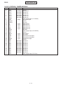
1
GX10i
CONFIDENTIAL
SERVICE MANUAL
No. S4305TQGX15/A
DIGITAL MOBILE PHONE
MODEL
GX10i
(INTERNAL MODEL NAME:
TQ-GX15E/G/R/T/S/H/EP/PP/W/B/D/A/Z/Q)
E : For U.K.
R : For Ireland
S : For Spain
EP : For U.K. (Prepaid)
W : For Sweden
D : For Greece
Z : For New Zealand
G :
T :
H :
PP :
B :
A :
Q :
For Germany
For Italy
For Netherlands
For Portugal (Prepaid)
For Hungary
For Australia
For Egypt
• In the interests of user-safety the set should be restored to its
original condition and only parts identical to those specified
should be used.
• Caution
Risk of explosion if battery is replaced by an incorrect type,
dispose of used batteries according to the instruction.
CONTENTS
CHAPTER 1. GENERAL DESCRIPTION
[1] Specifications ..............................................1-1
[2] Names of parts ............................................1-2
[3] Operation manual ........................................ 1-2
CHAPTER 2. ADJUSTMENTS
[1] Adjustments
SHARP Program Support Tool (SPST) .......2-1
[2] SHARP RF Test tool manual ..................... 2-30
[3] Adjustment procedures after replacement
of the parts ................................................2-36
[4] Test points .................................................2-38
[5] Troubleshooting ........................................ 2-42
[6] Specification for function test .................... 2-56
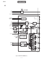
CHAPTER 4. DIAGRAMS
[1] Block diagram .............................................4-1
CHAPTER 5. SCHEMATIC DIAGRAM AND
WIRING SIDE OF P.W.BOARD
[1] Notes on schematic diagram ...................... 5-1
[2] Types of transistor and LED ........................5-1
[3] Waveforms of circuit ....................................5-2
[4] Schematic diagram/
wiring side of P.W.Board .............................5-6
CHAPTER 6. OTHERS
[1] Function table of IC .....................................6-1
PARTS GUIDE
CHAPTER 3. DISASSEMBLY AND
REASSEMBLY
[1] Servicing concerns ......................................3-1
[2] Disassembly and reassembly ..................... 3-2
SHARP CORPORATION
This document has been published to be used
for after sales service only.
The contents are subject to change without notice.
GX10i
CONFIDENTIAL
FOR A COMPLETE DESCRIPTION OF THE OPERATION OF THIS UNIT,
PLEASE REFER TO THE OPERATION MANUAL.
CHAPTER 1. GENERAL DESCRIPTION
[1] Specifications
General:
Tri - band (GSM 900 MHz/DCS 1800 MHz/
PCS 1900MHz)
GPRS-enabled
WAP, MMS, SMS
Dimensions (folded, excluding the aerial)
(H x W x D):
94 x 49 x 27 mm
Weight:
110 g
Battery operating
temperature:
0°C - 40°C
Main-screen
display:
Display dimensions: 160 x 120 dots
LCD display: TFT 65,536 colours with backlight
LCD backlight: LED backlight white colour LEDs
Sub-screen
display:
Display dimensions: 26 x 96 dots
LCD display: STN monochrome LCD with backlight
Camera:
CMOS 110K pixels built-in camera
Zoom: Wide and zoom mode
(Supported 2x zoom)
Lens: F2.0, f = 1.8 mm
Sound:
Status LED:
External DC
supply voltage:
Battery:
Standby time:
Talk time:
Others:
16-polyphonic ring melodies
Green and red
5.2 V
3.7 V, 720 mAh, Li-Ion
100 ~ 250 hours
150 ~ 240 min.
Side key
Infrared port 1.2 L/P (maximum distance 20 cm)
Connector for AC charger and data cable
Standard hands free connector (ø2.5)
Battery ranning time depends on the battery and SIM card as
well as the network conditions and usage.
Specifications for this model are subject to change without
prior notice.
Powered by JBlend R , C 1997-2003 Aplix Corporation. All
rights reserved.
Java and all Java-based trademarks and logos are trademarks or registered trademarks of Sun Microsystems, Inc.
in the U.S. and other countries.
JBlend and all JBlend-based trademarks and logos are
trademarks or registered trademarks of Aplix Corporation in
Japan and other countries.
Licensed by Inter Digital Technology Corporation under one
or more of the following United States Patents and/or their
domestic or foreign counterparts and other patents pending, including U.S. Patents: 4,675,863: 4,779,262:
4,785,450 & 4,811,420.
Licensed under U.S. Patent 4,558,302 and foreign
counterparts.
R
T9 Text input is licensed under one or more of the following:
U.S. Pat. Nos. 5,818,437, 5,953,541, 5,187,480, 5,945,928,
and 6,011,554; Australian Pat. No. 727539; Canadian Pat.
No. 1,331,057; United Kingdom Pat. No. 2238414B; Hong
Kong Standard Pat. No. HK0940329; Republic of
Singapore Pat. No. 51383; Euro. Pat. No. 0 842 463
(96927260.8) DE/DK, Fl, FR, IT, NL,PT.ES,SE,GB;
Republic or Korea Pat. Nos. KR201211B1 and
KR226206B1; and additional patents are pending
worldwide.
In this product, JBlend is incorporated.
R
JBlend is a Java execution environment
that Aplix developed for implementing
advanced performance and fast operation
on small-memory systems. JBlend and
JBlend logo are trademarks or registered
trademarks of Aplix Corporation in Japan
and other countries.
Powered by Mascot Capsule /Micro3D EditionTM
Mascot Capsule R is a registered trademark of HI Corporation
C 2002-2003 HI Corporation. All Rights Reserved.
R
1–1
2
GX10i
CONFIDENTIAL
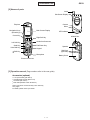
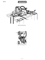
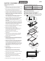
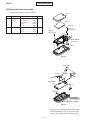
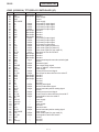
[2] Names of parts
Aerial
Sub-Screen Display
Earpiece
Camera
Mirror
Main-Screen Display
Navigation Keys
(Arrow Keys)
LED Indicator
Centre Key
Infrared Port
Right Soft Key
Hands free Connector
Left Soft Key
Send Key
Voice Mail Key
End/Power Key
Speaker
Keypad
Side Keys
(Up/Down)
/Shift Key
Microphone
Battery Cover
External Connector
[3] Operation manual (Page numbers refer to the user guide)
Accessories (optional)
Li-ion spare battery (XN-1BT11)
Cigarette lighter charger (XN-1CL10)
Car holder (XN-1CH11)
Data cable (RS232C cable: XN-1DC10)
Some of the above accessories may not be offered by
every region.
For details, please contact your dealer.
1–2
3
1–3
4
always returns you to Phone mode.
Sending: From the text entry screen:
1. Press
, and key in a mobile number (or an email address:
to enter text first press and hold
– to get the @ symbol,
press the
key 3 times).
2. Press
, choose “Send” and press
[Select].
Note: Repeat the same steps, choosing “Sound” instead of
“Picture” to attach a sound – for instance a voice memo from
yourself (see Section M5-4, p.75 on how to record).
Attaching your photo:
1. Press
[Options]. Select “Picuture”
and press
.
2. Choose the photo you want. Press
.
3. Press
[Back] to go back to your message.
Shoot
Sh
oot
136
4. Select “Stormy Sight”, and press
to play.
You can download further JavaTM games by selecting “Download
More” in the “JavaTM Games” menu. This will take you to the
Vodafone live! portal (see next page).
Your phone comes with two built-in games
and one pre-loaded JavaTM game: Stormy
Sight. To try out the enhanced gameplay
of this JavaTM game, go to the Main Menu:
1. Select “Fun & Games”, and press
.
2. Select “JavaTM Games”, and press
.
3. Select “Saved Games”, and press
.
Download a new ringtone: You can also download one of the
many amazing new polyphonic ringtones, which the download will
store in the “My Sounds” folder in the “My Phone” section of the
Main Menu.
First you need to access the Vodafone live! portal.
More...
Chat
Games
Messages
Downloads
New
Playing games
4. Press
and write your text
message.
Sh
oot
Shoot
3. Press
Choosing a ringtone:
1. From the Main Menu select “Profiles”, select “Normal”,
then go to “Edit” and press
.
2. Select “Assign Melody”,
then “Preset Melody” and press
. Choose a melody.
3. To hear it, select
[Play]. To stop, press
[Stop].
4. If you like it, you can press
to select. Or try out another
ringtone.
1. Your phone is already set up to use the mobile internet
browser. On the start-up screen you’ll see the Vodafone live!
logo
at the bottom right . Press
to select it,
and this will start the connection process (see the Vodafone
section, p.105).
2. Once connected you'll see a menu of icons which take you to
different areas of the portal for you to explore.
3. To download a ringtone, go to
“Downloads” and follow the prompts to
listen to and download a new ringtone.
You can now choose it on your phone as
before.
The tip of the iceberg: This portal has a
whole world of news and entertainment to
offer you. For more details, please refer to
the Vodafone live! guide.
The Sharp GX10i comes with a range of amazing ringtones
already loaded for you to try out.
Tip: Try sending to yourself to see how it works.
Problems? You may need to be registered for MMS – speak to
Vodafone customer services.
Use the MMS (Multi Media Messaging) function to send your
photo together with a text message.
1. From the Main Menu scroll up to “Messages”.
2. Press
and select “MMS”.
and select “Compose”.
Accessing the Vodafone live! portal
[Select].
Polyphonic Ringtones
, and select your photo from the list.
4. Press
“Wallpaper”,
3. Press
Using a photo as wallpaper:
1. Go to the Main Menu.
2. Select “Settings”,
“Phone Settings”,
“On”,
“My Pictures”.
Viewing photos:
1. In Camera mode, press
[Options].
2. Select “Existing Pictures”, then press
.
3. Go to the picture file you want to view (they’re named by time
and date), and press
.
Note:
3. You’ll be asked to OK the file size: select “Yes”, press
and watch it being sent.
137
[Save] (“Save to My Phone” is shown), or press
to Send your picture to someone else (see next page). Or
press
[Back] instead to re-take.
3. Press
Taking a photo:
1. From the start-up screen, press and hold for two seconds
to go into Camera mode (see Section M1: Camera, p.34 for full
details).
2. Press
to capture the image on screen.
Using the camera
Picture Messaging
,
135
takes you back to a previous
menu.
The
‘soft’ keys select
whatever is at the bottom left and right of
the screen – often as an alternative to
the menu keys.
Navigation and selection:
The GX10i uses icons to help you
navigate (like on your PC).
Press the central silver
key to
access the icons on the Main Menu.
Use
to move up and down the
on-screen menus, and the
key or
to select.
Turning it on: Press and hold the
red key for two seconds (the same to turn
off).
OK. Your SIM card’s in the handset, and
you’ve charged the battery (see “Getting
Started”, p.8).
Trying out your phone
QUICKSTART GUIDE: RINGTONES & PORTAL
134
Access the Vodafone live! portal
We’ll also show you how to connect up to the
Vodafone live! portal, to discover what the world’s
largest mobile community has to offer you and your
phone: from new ringtones to games,
entertainment and news services.
In which case, the next three pages will show you how to:
Take your first picture with the camera
Send it as a multimedia message with text
Try out a JavaTM game using
animation, 2D and 3D effects
Experiment with ringtones, and...
QUICKSTART GUIDE: NAVIGATION & CAMERA
QUICKSTART GUIDE: MESSAGING & GAMES
How to do all this is described in detail inside this
manual. But if you are already familiar with how
a mobile phone works, you probably want to try
out the new features straight away – the things
you couldn’t do before.
For instance:
Taking and sending colour photos
Playing arcade quality games
Amazing your friends with polyphonic ringtones
Accessing the mobile internet quickly and easily
Congratulations on your new Sharp GX10i. With this advanced
handset, you will be able to do far more than “talk and text”. Now
you can take full advantage of all the new Vodafone live!
services.
More than voice and text – now it’s pictures, music and games!
QUICKSTART GUIDE: INTRODUCTION
GX10i
CONFIDENTIAL
CONFIDENTIAL
GX10i
CHAPTER 2. ADJUSTMENTS
[1] Adjustments
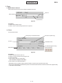
SHARP Program Support Tool (SPST)
1. Outline
This document provides user information required to install and use GX10i Program Support Tool (SPST).
2. System requirements
• IBM PC compatible personal computer (standard COM1 serial port (115,200 bps) and USB required)
Supporting OS: Windows 98/98SE/2000/XP (except for Windows 95/ME/NT)
(English, German, Italian, Spanish, French and Chinese versions)
• Data cable
• Full charged battery
<During RF adjustment>
• RF test instrument: CMU200, CMD55
• GPIB interface: National Instruments USB-GPIB cable
Model No.: NI GPIB-USB-B
• The battery should be fully charged.
3. Introduction
3.1 Functions
SPST offers five key functions:
1. Software download
2. User data transfer (processes all data at once but not individually)
3. RF calibration
4. Default setting
5. Identification
SPST functions as a launcher for these independent software programs.
3.2 Installation
The SPST software is distributed in CD-ROM format.
(1) Use Windows Explorer and copy “UpgradingTool.zip” and “SPST.zip” to the desktop.
(2) Unzip and install “UpgradingTool.zip” following the procedures below.
(3) Unzip the “SPST.zip”.
Hereinafter, procedures are carried out in the SPST folder.
3.2.1 Starting up
Connect GX10i to an operable serial port of the PC with the supplied data cable. Connect the AC charger to the data cable.
Execute the GX10i SPST.exe program in the SPST folder.
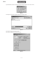
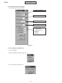
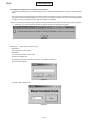
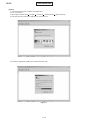
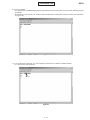
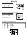
(1) The SPC input screen appears. Input SPC (2968) and press “OK”.
If you do not know SPC, press “Cancel” to close.
Figure 1
2–1
GX10i
CONFIDENTIAL
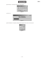
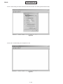
(2) If SPC is correct, the following screen appears.
Figure 2
The software for each function is independent and thus multi-bootable. However, you can only activate single software at
a time. To start snother software, exit the current one.
3.3. Functions
3.3.1 Identification
SPST downloads and displays the main data configured in GX10i.
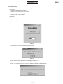
<Operation>
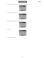
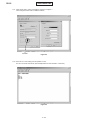
(1) On the SPST startup screen, press “Identity”.
Figure 3
(2) Connect PC and MS with a Data cable.
(3) Remove the SIM card and turn on the phone.
Regular display.
(4) Select the COM port.
(5) Press “Get Identity”.
The information will be displayed.
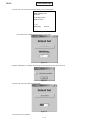
(6) IMEI will be displayed, and the following dialog box appears.
Figure 4
(7) Make sure GX10i is turned off and press the power key.
(8) Press “OK” when **** appears on the GX10i display.
2–2
GX10i
CONFIDENTIAL
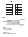
(9) Make sure “Success!!” appears. Check the data and exit.
Refer to the attachment 1
for the operator code.
Software version:
IMEISV: 02
Figure 5
Attachment 1
Operator Code Chart
No.
01
Operator name
Vodafone UK
Post-Paid
02
04
Airtel
Vodafone Omnitel
05
06
Vodafone D2
Vodafone NL
08
10
Vodafone Ireland
Vodafone Greece
48
50
Vodafone PT
Vodafone UK
12
13
15
Vodafone Australia
Vodafone New Zealand
Vodafone Egypt
Post-Paid
14
11
Vodafone Sweden
Vodafone Hungary
Country
UK
Model name
A4TQGX15E
Spain
Italy
A4TQGX15S
A4TQGX15T
Germany
Netherlands(Holland)
A4TQGX15G
A4TQGX15H
Ireland
Greece
A4TQGX15R
A4TQGX15D
Portugal
UK
A4TQGX15PP
A4TQGX15EP
Australia
New Zealand
Egypt
A4TQGX15A
A4TQGX15Z
A4TQGX15Q
Sweden
Hungary
A4TQGX15W
A4TQGX15B
Pre-Paid
Pre-Paid
Post-Paid
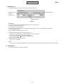
3.3.2 User data transfer
SPST saves and downloads all the following user data.
(1) Connect PC and MS with a Data cable and turn on MS.
(2) Activate the software.
Figure 6
1. Select the COM port. You cannot specify the communication protocol. (115 kbps)
2. Press “Recognition”.
Do not press “Recognition” until “InsertSIM” appears.
2–3
GX10i
CONFIDENTIAL
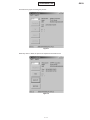
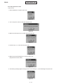
(3) Press either “BACKUP”, “RESTORE” or “END”.
Figure 7
(4) If “BACKUP” is pressed, the dialog box for file selection appears. Select the file and press “Save”.
Figure 8
2–4
CONFIDENTIAL
The buttons are grayed out during the process.
Figure 9
When they return to black, the process is complete. Press “END” to exit.
Figure 10
2–5
GX10i
GX10i
CONFIDENTIAL
(5) If “RESTORE” is pressed, the following confirmation dialog box appears. Press “OK” to confirm.
Figure 11
The dialog box for file selection appears. Select the file and press “Open”.
Figure 12
The buttons are grayed out during the process.
The process is complete when the buttons turn black.
Figure 13
2–6
CONFIDENTIAL
3.3.3 Default setting
SPST can restore the factory settings by default setting.
This function
1. deletes all user data in the file system;
2. restores the values set by the user to default;
3. restores all WAP and MMS settings to default; and
4. restores all MEP_LOCK to default.
<Operation>
(1) Connect the phone to a cable.
(2) Turn on the phone and wait until it enters the idle mode.
(3) Press “Set to Default”.
Figure 14
(4) The phone turns off and the following message appears.
Figure 15
(5) When the power key is pressed, the screen display will display “****”.
(6) When “OK” is pressed on the PC screen, the following confirmation message appears.
Figure 16
2–7
GX10i
GX10i
CONFIDENTIAL
(7) Press “OK”. You will see the following display on the screen display.
H/W CHECK
∗ GX-10i ∗
ROM VERSION : 007
BLCD:48
Gx10i diag version.
2002.09.10 v23
T_2.3
2003/04/24
11:05:48
Figure 17
Check the version. Initialization takes approx. 35 seconds.
Figure 18
(8) When initialization is complete, the following message appears and the phone turns off.
Figure 19
(9) Press “OK” to proceed. Disconnect the cable.
Figure 20
The process is now completed.
2–8
GX10i
CONFIDENTIAL
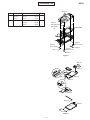
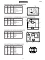
3.3.4 RF Adjustment Tool
GSM tester
MS
GPIB cable
Cable loss should be adjusted
according to the input value.
Data cable
PC
Figure 21
3.3.4.1. Preparation
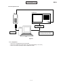
• Connect PC and GSM tester with a GPIB cable.
• Connect PC and MS with a Data cable. (Use a full charged battery or one close.)
• Connect an antenna input/output cable of GSM tester to MS.
2–9
GX10i
CONFIDENTIAL
3.3.4.2. Default setting for the program.
• Activate the program and set defaults.
1) Select the COM port.
2) Set the GPIB No.
3) Select the test instrument.
4) Set the GPIB address.
5) Set the cable loss. For the
supplied cables
(YA00-0988-03), set:
GSM 0.60
DCS 0.95
PCS 0.96
Figure 22
3.3.4.3 RF adjustment (CMU200 only)
1. Press “Calibration”.
2. When initialization is complete, press “OK”.
Figure 23
3. Turn on the phone and press “OK”.
Figure 24
2 – 10
CONFIDENTIAL
4. Make sure that the phone is in the idle mode and press “OK”. (Adjustments start.)
Figure 25
5. Turn on the phone and press “OK”.
Figure 26
6. Make sure the phone is turned on and press “OK”.
Figure 27
7. Press “OK”.
Figure 28
8. The startup screen appears.
2 – 11
GX10i
GX10i
CONFIDENTIAL
3.3.4.4 RF performance check
Press “Check”.
1. When initialization is complete, press “OK”.
Figure 29
2. Turn on the phone, enter the PIN code and press “OK”.
Figure 30
3. Make sure that the phone is in the idle mode and press “OK”.
Figure 31
4. Press the keys 1, 2, 3 and Send and press “OK”.
Figure 32
5. Make sure the terminal display is “In Call” and press “OK”.
(RF performance check starts.)
Figure 33
6. The following message appears during the check. Press the keys 1, 2, 3 and Send again and press “OK”.
Figure 34
2 – 12
CONFIDENTIAL
GX10i
7. Make sure the terminal display is “In Call” and press “OK”.
Figure 35
8. RF performance check is complete. Press “Save As…”and name the file to save the result. Press “OK” to exit.
Figure 36
The following will be displayed in case of failure.
Figure 37
9. Press “OK”.
Figure 38
10. The startup screen appears.
2 – 13
GX10i
CONFIDENTIAL
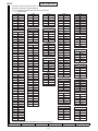
Attachment 2
Whole inspection list by RF performance check.
Sending/
Channel
Band Receive No. Item to be inspected
GSM
Tx
1 Sending output
37CH
band
2 Sending output
975CH
3 Sending output
124CH
4 Sending output
37CH
5 Sending output
37CH
6 Frequency deviation
37CH
7 Frequency deviation
975CH
8 Frequency deviation
124CH
9 Phase error (RMS)
37CH
10 Phase error (RMS)
975CH
11 Phase error (RMS)
124CH
12 Phase error (Peak)
37CH
13 Phase error (Peak)
975CH
14 Phase error (Peak)
124CH
15 Mod_spectrum –800
37CH
16 Mod_spectrum –600
37CH
17 Mod_spectrum –400
37CH
18 Mod_spectrum –250
37CH
19 Mod_spectrum –200
37CH
20 Mod_spectrum +200
37CH
21 Mod_spectrum +250
37CH
22 Mod_spectrum +400
37CH
23 Mod_spectrum +600
37CH
24 Mod_spectrum +800
37CH
25 Mod_spectrum –800
975CH
26 Mod_spectrum –600
975CH
27 Mod_spectrum –400
975CH
28 Mod_spectrum –250
975CH
29 Mod_spectrum –200
975CH
30 Mod_spectrum +200
975CH
31 Mod_spectrum +250
975CH
32 Mod_spectrum +400
975CH
33 Mod_spectrum +600
975CH
34 Mod_spectrum +800
975CH
35 Mod_spectrum –800
124CH
36 Mod_spectrum –600
124CH
37 Mod_spectrum –400
124CH
38 Mod_spectrum –250
124CH
39 Mod_spectrum –200
124CH
40 Mod_spectrum +200
124CH
41 Mod_spectrum +250
124CH
42 Mod_spectrum +400
124CH
43 Mod_spectrum +600
124CH
44 Mod_spectrum +800
124CH
45 Mod_spectrum –800
37CH
46 Mod_spectrum –600
37CH
47 Mod_spectrum –400
37CH
48 Mod_spectrum –250
37CH
49 Mod_spectrum –200
37CH
50 Mod_spectrum +200
37CH
51 Mod_spectrum +250
37CH
52 Mod_spectrum +400
37CH
53 Mod_spectrum +600
37CH
54 Mod_spectrum +800
37CH
55 Mod_spectrum –800
37CH
56 Mod_spectrum –600
37CH
57 Mod_spectrum –400
37CH
58 Mod_spectrum –250
37CH
59 Mod_spectrum –200
37CH
60 Mod_spectrum +200
37CH
61 Mod_spectrum +250
37CH
62 Mod_spectrum +400
37CH
63 Mod_spectrum +600
37CH
64 Mod_spectrum +800
37CH
65 Switch_Spectrum –1800 37CH
66 Switch_Spectrum –1200 37CH
67 Switch_Spectrum –600
37CH
68 Switch_Spectrum –400
37CH
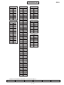
Sending/
Band Receive No.
69
70
71
72
73
74
75
76
77
78
79
80
81
82
83
84
85
86
87
88
89
90
91
92
93
94
95
96
97
98
99
100
101
102
103
104
105
106
107
108
109
Rx 110
111
112
113
114
DCS
Tx 115
band
116
117
118
119
120
121
122
123
124
125
126
127
128
129
130
131
132
133
134
135
PCL
PCL5
PCL5
PCL5
PCL11
PCL19
PCL5
PCL5
PCL5
PCL5
PCL5
PCL5
PCL5
PCL5
PCL5
PCL5
PCL5
PCL5
PCL5
PCL5
PCL5
PCL5
PCL5
PCL5
PCL5
PCL5
PCL5
PCL5
PCL5
PCL5
PCL5
PCL5
PCL5
PCL5
PCL5
PCL5
PCL5
PCL5
PCL5
PCL5
PCL5
PCL5
PCL5
PCL5
PCL5
PCL11
PCL11
PCL11
PCL11
PCL11
PCL11
PCL11
PCL11
PCL11
PCL11
PCL19
PCL19
PCL19
PCL19
PCL19
PCL19
PCL19
PCL19
PCL19
PCL19
PCL5
PCL5
PCL5
PCL5
2 – 14
Item to be inspected
Channel
PCL
Switch_Spectrum +400
Switch_Spectrum +600
Switch_Spectrum +1200
Switch_Spectrum +1800
Switch_Spectrum –1800
Switch_Spectrum –1200
Switch_Spectrum –600
Switch_Spectrum –400
Switch_Spectrum +400
Switch_Spectrum +600
Switch_Spectrum +1200
Switch_Spectrum +1800
Switch_Spectrum –1800
Switch_Spectrum –1200
Switch_Spectrum –600
Switch_Spectrum –400
Switch_Spectrum +400
Switch_Spectrum +600
Switch_Spectrum +1200
Switch_Spectrum +1800
Switch_Spectrum –1800
Switch_Spectrum –1200
Switch_Spectrum –600
Switch_Spectrum –400
Switch_Spectrum +400
Switch_Spectrum +600
Switch_Spectrum +1200
Switch_Spectrum +1800
Switch_Spectrum –1800
Switch_Spectrum –1200
Switch_Spectrum –600
Switch_Spectrum –400
Switch_Spectrum +400
Switch_Spectrum +600
Switch_Spectrum +1200
Switch_Spectrum +1800
Burst Timing
Burst Timing
Burst Timing
Burst Timing
Burst Timing
Reception sensitivity
Reception sensitivity
Reception sensitivity
Floor sensitivity 2
Reception level report
Sending output
Sending output
Sending output
Sending output
Sending output
Frequency deviation
Frequency deviation
Frequency deviation
Phase error (RMS)
Phase error (RMS)
Phase error (RMS)
Phase error (Peak)
Phase error (Peak)
Phase error (Peak)
Mod_spectrum –800
Mod_spectrum –600
Mod_spectrum –400
Mod_spectrum –250
Mod_spectrum –200
Mod_spectrum +200
Mod_spectrum +250
37CH
37CH
37CH
37CH
975CH
975CH
975CH
975CH
975CH
975CH
975CH
975CH
124CH
124CH
124CH
124CH
124CH
124CH
124CH
124CH
37CH
37CH
37CH
37CH
37CH
37CH
37CH
37CH
37CH
37CH
37CH
37CH
37CH
37CH
37CH
37CH
37CH
975CH
124CH
37CH
37CH
37CH
975CH
124CH
37CH
37CH
699CH
512CH
855CH
699CH
699CH
699CH
512CH
855CH
699CH
512CH
855CH
699CH
512CH
855CH
699CH
699CH
699CH
699CH
699CH
699CH
699CH
PCL5
PCL5
PCL5
PCL5
PCL5
PCL5
PCL5
PCL5
PCL5
PCL5
PCL5
PCL5
PCL5
PCL5
PCL5
PCL5
PCL5
PCL5
PCL5
PCL5
PCL11
PCL11
PCL11
PCL11
PCL11
PCL11
PCL11
PCL11
PCL19
PCL19
PCL19
PCL19
PCL19
PCL19
PCL19
PCL19
PCL5
PCL5
PCL5
PCL11
PCL19
PCL5
PCL5
PCL5
PCL5
PCL5
PCL0
PCL0
PCL0
PCL5
PCL15
PCL0
PCL0
PCL0
PCL0
PCL0
PCL0
PCL0
PCL0
PCL0
PCL0
PCL0
PCL0
PCL0
PCL0
PCL0
PCL0
GX10i
CONFIDENTIAL
Sending/
Band Receive No.
136
137
138
139
140
141
142
143
144
145
146
147
148
149
150
151
152
153
154
155
156
157
158
159
160
161
162
163
164
165
166
167
168
169
170
171
172
173
174
175
176
177
178
179
180
181
182
183
184
185
186
187
188
189
190
191
192
193
194
195
196
197
198
199
200
201
202
203
Item to be inspected
Channel
PCL
Mod_spectrum +400
Mod_spectrum +600
Mod_spectrum +800
Mod_spectrum –800
Mod_spectrum –600
Mod_spectrum –400
Mod_spectrum –250
Mod_spectrum –200
Mod_spectrum +200
Mod_spectrum +250
Mod_spectrum +400
Mod_spectrum +600
Mod_spectrum +800
Mod_spectrum –800
Mod_spectrum –600
Mod_spectrum –400
Mod_spectrum –250
Mod_spectrum –200
Mod_spectrum +200
Mod_spectrum +250
Mod_spectrum +400
Mod_spectrum +600
Mod_spectrum +800
Mod_spectrum –800
Mod_spectrum –600
Mod_spectrum –400
Mod_spectrum –250
Mod_spectrum –200
Mod_spectrum +200
Mod_spectrum +250
Mod_spectrum +400
Mod_spectrum +600
Mod_spectrum +800
Mod_spectrum –800
Mod_spectrum –600
Mod_spectrum –400
Mod_spectrum –250
Mod_spectrum –200
Mod_spectrum +200
Mod_spectrum +250
Mod_spectrum +400
Mod_spectrum +600
Mod_spectrum +800
Switch_Spectrum –1800
Switch_Spectrum –1200
Switch_Spectrum –600
Switch_Spectrum –400
Switch_Spectrum +400
Switch_Spectrum +600
Switch_Spectrum +1200
Switch_Spectrum +1800
Switch_Spectrum –1800
Switch_Spectrum –1200
Switch_Spectrum –600
Switch_Spectrum –400
Switch_Spectrum +400
Switch_Spectrum +600
Switch_Spectrum +1200
Switch_Spectrum +1800
Switch_Spectrum –1800
Switch_Spectrum –1200
Switch_Spectrum –600
Switch_Spectrum –400
Switch_Spectrum +400
Switch_Spectrum +600
Switch_Spectrum +1200
Switch_Spectrum +1800
Switch_Spectrum –1800
699CH
699CH
699CH
512CH
512CH
512CH
512CH
512CH
512CH
512CH
512CH
512CH
512CH
855CH
855CH
855CH
855CH
855CH
855CH
855CH
855CH
855CH
855CH
699CH
699CH
699CH
699CH
699CH
699CH
699CH
699CH
699CH
699CH
699CH
699CH
699CH
699CH
699CH
699CH
699CH
699CH
699CH
699CH
699CH
699CH
699CH
699CH
699CH
699CH
699CH
699CH
512CH
512CH
512CH
512CH
512CH
512CH
512CH
512CH
855CH
855CH
855CH
855CH
855CH
855CH
855CH
855CH
699CH
PCL0
PCL0
PCL0
PCL0
PCL0
PCL0
PCL0
PCL0
PCL0
PCL0
PCL0
PCL0
PCL0
PCL0
PCL0
PCL0
PCL0
PCL0
PCL0
PCL0
PCL0
PCL0
PCL0
PCL5
PCL5
PCL5
PCL5
PCL5
PCL5
PCL5
PCL5
PCL5
PCL5
PCL15
PCL15
PCL15
PCL15
PCL15
PCL15
PCL15
PCL15
PCL15
PCL15
PCL0
PCL0
PCL0
PCL0
PCL0
PCL0
PCL0
PCL0
PCL0
PCL0
PCL0
PCL0
PCL0
PCL0
PCL0
PCL0
PCL0
PCL0
PCL0
PCL0
PCL0
PCL0
PCL0
PCL0
PCL5
Sending/
Band Receive No.
204
205
206
207
208
209
210
211
212
213
214
215
216
217
218
219
220
221
222
223
Rx 224
225
226
227
228
PCS
Tx 229
band
230
(CMU
231
200
232
only)
233
234
235
236
237
238
239
240
241
242
243
244
245
246
247
248
249
250
251
252
253
254
255
256
257
258
259
260
261
262
263
264
265
266
267
268
269
270
2 – 15
Item to be inspected
Channel
PCL
Switch_Spectrum –1200
Switch_Spectrum –600
Switch_Spectrum –400
Switch_Spectrum +400
Switch_Spectrum +600
Switch_Spectrum +1200
Switch_Spectrum +1800
Switch_Spectrum –1800
Switch_Spectrum –1200
Switch_Spectrum –600
Switch_Spectrum –400
Switch_Spectrum +400
Switch_Spectrum +600
Switch_Spectrum +1200
Switch_Spectrum +1800
Burst Timing
Burst Timing
Burst Timing
Burst Timing
Burst Timing
Reception sensitivity
Reception sensitivity
Reception sensitivity
Floor sensitivity 2
Reception level report
Sending output
Sending output
Sending output
Sending output
Sending output
Frequency deviation
Frequency deviation
Frequency deviation
Phase error (RMS)
Phase error (RMS)
Phase error (RMS)
Phase error (Peak)
Phase error (Peak)
Phase error (Peak)
Mod_spectrum –800
Mod_spectrum –600
Mod_spectrum –400
Mod_spectrum –250
Mod_spectrum –200
Mod_spectrum +200
Mod_spectrum +250
Mod_spectrum +400
Mod_spectrum +600
Mod_spectrum +800
Mod_spectrum –800
Mod_spectrum –600
Mod_spectrum –400
Mod_spectrum –250
Mod_spectrum –200
Mod_spectrum +200
Mod_spectrum +250
Mod_spectrum +400
Mod_spectrum +600
Mod_spectrum +800
Mod_spectrum –800
Mod_spectrum –600
Mod_spectrum –400
Mod_spectrum –250
Mod_spectrum –200
Mod_spectrum +200
Mod_spectrum +250
Mod_spectrum +400
699CH
699CH
699CH
699CH
699CH
699CH
699CH
699CH
699CH
699CH
699CH
699CH
699CH
699CH
699CH
699CH
512CH
855CH
699CH
699CH
699CH
512CH
855CH
699CH
699CH
661CH
512CH
810CH
661CH
661CH
661CH
512CH
810CH
661CH
512CH
810CH
661CH
512CH
810CH
661CH
661CH
661CH
661CH
661CH
661CH
661CH
661CH
661CH
661CH
512CH
512CH
512CH
512CH
512CH
512CH
512CH
512CH
512CH
512CH
810CH
810CH
810CH
810CH
810CH
810CH
810CH
810CH
PCL5
PCL5
PCL5
PCL5
PCL5
PCL5
PCL5
PCL15
PCL15
PCL15
PCL15
PCL15
PCL15
PCL15
PCL15
PCL0
PCL0
PCL0
PCL5
PCL15
PCL0
PCL0
PCL0
PCL0
PCL0
PCL0
PCL0
PCL0
PCL5
PCL15
PCL0
PCL0
PCL0
PCL0
PCL0
PCL0
PCL0
PCL0
PCL0
PCL0
PCL0
PCL0
PCL0
PCL0
PCL0
PCL0
PCL0
PCL0
PCL0
PCL0
PCL0
PCL0
PCL0
PCL0
PCL0
PCL0
PCL0
PCL0
PCL0
PCL0
PCL0
PCL0
PCL0
PCL0
PCL0
PCL0
PCL0
GX10i
CONFIDENTIAL
Sending/
Band Receive No.
271
272
273
274
275
276
277
278
279
280
281
282
283
284
285
286
287
288
289
290
291
292
293
294
295
296
297
298
299
300
301
302
303
304
305
306
Item to be inspected
Channel
PCL
Mod_spectrum +600
Mod_spectrum +800
Mod_spectrum –800
Mod_spectrum –600
Mod_spectrum –400
Mod_spectrum –250
Mod_spectrum –200
Mod_spectrum +200
Mod_spectrum +250
Mod_spectrum +400
Mod_spectrum +600
Mod_spectrum +800
Mod_spectrum –800
Mod_spectrum –600
Mod_spectrum –400
Mod_spectrum –250
Mod_spectrum –200
Mod_spectrum +200
Mod_spectrum +250
Mod_spectrum +400
Mod_spectrum +600
Mod_spectrum +800
Switch_Spectrum –1800
Switch_Spectrum –1200
Switch_Spectrum –600
Switch_Spectrum –400
Switch_Spectrum +400
Switch_Spectrum +600
Switch_Spectrum +1200
Switch_Spectrum +1800
Switch_Spectrum –1800
Switch_Spectrum –1200
Switch_Spectrum –600
Switch_Spectrum –400
Switch_Spectrum +400
Switch_Spectrum +600
810CH
810CH
661CH
661CH
661CH
661CH
661CH
661CH
661CH
661CH
661CH
661CH
661CH
661CH
661CH
661CH
661CH
661CH
661CH
661CH
661CH
661CH
661CH
661CH
661CH
661CH
661CH
661CH
661CH
661CH
512CH
512CH
512CH
512CH
512CH
512CH
PCL0
PCL0
PCL5
PCL5
PCL5
PCL5
PCL5
PCL5
PCL5
PCL5
PCL5
PCL5
PCL15
PCL15
PCL15
PCL15
PCL15
PCL15
PCL15
PCL15
PCL15
PCL15
PCL0
PCL0
PCL0
PCL0
PCL0
PCL0
PCL0
PCL0
PCL0
PCL0
PCL0
PCL0
PCL0
PCL0
Sending/
Band Receive No.
307
308
309
310
311
312
313
314
315
316
317
318
319
320
321
322
323
324
325
326
327
328
329
330
331
332
333
334
335
336
337
RX 338
339
340
341
342
Item to be inspected
Channel
PCL
Switch_Spectrum +1200
Switch_Spectrum +1800
Switch_Spectrum –1800
Switch_Spectrum –1200
Switch_Spectrum –600
Switch_Spectrum –400
Switch_Spectrum +400
Switch_Spectrum +600
Switch_Spectrum +1200
Switch_Spectrum +1800
Switch_Spectrum –1800
Switch_Spectrum –1200
Switch_Spectrum –600
Switch_Spectrum –400
Switch_Spectrum +400
Switch_Spectrum +600
Switch_Spectrum +1200
Switch_Spectrum +1800
Switch_Spectrum –1800
Switch_Spectrum –1200
Switch_Spectrum –600
Switch_Spectrum –400
Switch_Spectrum +400
Switch_Spectrum +600
Switch_Spectrum +1200
Switch_Spectrum +1800
Burst Timing
Burst Timing
Burst Timing
Burst Timing
Burst Timing
Reception sensitivity
Reception sensitivity
Reception sensitivity
Floor sensitivity 2
Reception level report
512CH
512CH
810CH
810CH
810CH
810CH
810CH
810CH
810CH
810CH
661CH
661CH
661CH
661CH
661CH
661CH
661CH
661CH
661CH
661CH
661CH
661CH
661CH
661CH
661CH
661CH
661CH
512CH
810CH
661CH
661CH
661CH
512CH
810CH
661CH
661CH
PCL0
PCL0
PCL0
PCL0
PCL0
PCL0
PCL0
PCL0
PCL0
PCL0
PCL5
PCL5
PCL5
PCL5
PCL5
PCL5
PCL5
PCL5
PCL15
PCL15
PCL15
PCL15
PCL15
PCL15
PCL15
PCL15
PCL0
PCL0
PCL0
PCL5
PCL15
PCL0
PCL0
PCL0
PCL0
PCL0
Troubleshooting list according to the results of RF performance check.
Check parts for GSM
Check parts for DCS
Tx
Sending output
Frequency deviation
Phase error
Mod_spectrum
Switch_spectrum
Burst Timing
Test item
IC831, IC881, FL811, FL801
TCX951
VCO971, IC901, VCO851
VCO971, IC901, VCO851
VCO971, IC901, VCO851
IC881
IC831, IC881, FL816, FL801
TCX951
VCO971, IC901, VCO851
VCO971, IC901, VCO851
VCO971, IC901, VCO851
IC881
Sprious
Rx
Not tested
Reception sensitivity
Floor sensitivity
Reception level report
FL801, FL901
FL801, FL901
FL801, FL901
FL801, FL902
FL801, FL902
FL801, FL902
2 – 16
GX10i
CONFIDENTIAL
3.3.5 Software download
(1) Overview
This document describes the specification of the Flash-downloading tool (an upgrading tool) for user service.
(2) Purpose of this document
The aim of this document is to provide a sufficient description of the GX10i Upgrading Tool for readers.
(3) Scope
This document covers the description of the Flash-downloading tool specification for user service.
(4) Operating environment
Operating environment for the upgrading tool
OS: Windows 98, 98SE, 2000 or XP
Downloadable file: Motorola format files only
Communication mode: Asynchronous mode
Data length: 8 bit
Parity bit: None
Stop bit length: 1 bit
Baud rate: 9600 bps (only at the time of activation)
28800 bps (While downloading the loader)
115200 bps (While in the normal operation)
Operating environment for the loader
Phone: GX10i
Communication mode: Asynchronous mode
Data length: 8 bit
Parity bit: None
Stop bit length: 1 bit
Baud rate: 9600 bps (only when activating)/115200 bps (While in the normal operation)
3.3.5.1 Description of the screens.
(1) Activation
You can start the application either from the short cut on your desktop or Start menu.
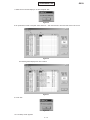
(2) The Upgrading Tool (on the PC)
Tick here if you wish to use
“CommunicationBoxVer2G”.
Note 1)
Tick here if you wish
to initialize the file system.
COM port list
Available when
“CommunicationBoxVer2G”is set.
Note 2)
Figure 39
2 – 17
Click this to display the
dialog box to select a file
to download.
GX10i
CONFIDENTIAL
Note 1)
If using “communicationBoxVer. 2G”, you can control only the phone connected to No.1 cable.
Note2)
Time displayed in this dialog box indicates a margin of processing time taken to download the data to phones that
are connected to cable No.2 to No.10 of the “communicationBoxVer. 2G”. If an error occurs, increase this margin.
For details, see the section 3.3.5.2 (3) “Using the Communication Box Ver. 2G” on page 2-20.
[Caution!]
• If you wish to download using “communicationBoxVer. 2G”, turn on No.10 to No.1 after “Sending Sync Byte…/Press
Power Button” message appears.
• To downloading by “communicationBoxVer. 2G”, remove the battery first. There will be no damage to the phone
even if the battery is inserted. However, the software on the phone may not terminate. In this case, remove the
battery to turn off the phone after the download is ended.
• Use a fully charged battery for the downloading operation.
Remove the battery from the phone to terminate the software after the download is completed.
• Start downloading after phone is properly turned off in order to clear the Backup RAM.
• Note that if you select “FileSystem Initialize”, the data stored in the phone will be deleted.
(3) The loader (in the phone)
The operation progress indication and error status are displayed on the phone.
The following are example screens.
1. Initial screen
Flash Loader 1.07
2. Deleting the Flash
Flash Loader 1.07
##########
P ERASING ...
3. Writing the data
Flash Loader 1.07
WRITING ...
P indicates a program data. To
indicate the data area, “D
ERASEING” is displayed.
The version of the loader is
displayed when it is successfully expanded.
4. Data writing is completed
The Flash is being erased. “#”
decreases as the erasing operation
proceeds, and disappears when it is
completed.
5. SUM value is indicated Note 1)
The data is being written into
the handset.
6. Error screen Note 2)
Flash Loader 1.07
Flash Loader 1.07
Flash Loader 1.07
COMPLETE!
SUMCHECK END
SUM = XXXX h
ERS_ERROR!
ADR = 1000000
STR = A0
The program data is successfully loaded.
SUM value is displayed a few
seconds after the program data
is successfully loaded.
The value is displayed at “XXXX”.
An error occurred.
ADR: Address the location of
the error.
STR: Flash Status information
Note 1)
You can check if the loaded program data is correct by comparing the SUM values displayed on the PC and the
phone shown on the screen 5. If both values are the same, the correct program data is loaded.
Note 2)
The screen 6 shows an error which occurred while erasing the Flash.
“ADR” and “STR” appear only for Flash-oriented errors. Other errors are described in the latter section.
2 – 18
CONFIDENTIAL
GX10i
3.3.5.2 Operational specification
(1) Selecting a file
Press “Select File” to open the dialog box. Select a file you wish to download.
You can select only the file in Motorola format.
Figure 40 The dialog box to select a file
(2) Selecting COM port.
Select the COM port from COM1 to COM9 that connects the PC and phone (or “communicationBoxVer . 2G”).
Figure 41 COM Port selecting screen
2 – 19
GX10i
CONFIDENTIAL
(3) Using the Communication Box Ver. 2G.
Tick “Use Communication Box Ver.2G” in the dialog box if using “Communication Box Ver.2G”. For details, see the
section 3.3.5.1 (2) “The Upgrading Tool (on the PC)” on page 2-17.
You can select wait time from 0 to 999 seconds since the access latency differs depending on the phone if using
“Communication Box Ver.2G”. (Default value is set to 100 seconds). For details on setting the wait time, see the section
3.3.5.1 (2) “The Upgrading Tool (on the PC)” on page 2-17.
Serial connection port
Power On/Off
button.
Set it to OFF for
default setting.
Cable 1.
Figure 42 Image of Communication Box Ver. 2G
[Caution]
Cable 1 is used for handshaking between the PC and phone. Make sure the cable is properly connected to the
phone during the handshaking if using “Communication Box Ver.2G”.
Switch on the power buttons No.10 to No.1 when “Sending Sync Byte…/Press Power Button” appears.
2 – 20
CONFIDENTIAL
GX10i
(4) Starting the downloading operation
Press [Start Loading Flash] button after you select the file to download.
The downloading operation starts. The message below appears if no file is selected.
Figure 43
[Using a Data cable]
If using a Data cable for the downloading operation, press Power button of the phone after [Please remove AC
charger, when you use PCcableSending Sync Byte…/Press Power Button!] appears. The loader starts to
activate.
[Using “Communication Box Ver. 2G”]
If using “Communication Box Ver. 2G”, switch on the power buttons No.10 to No.1 after [Please remove AC
charger, when you use PCcableSending Sync Byte…/Press Power Button!] appears. The loader starts to
activate.
[Caution]
If using a Data cable, [Sync received ; Sending RAM Loader.../Keep Power Button! ] message will appear after
the power button of the phone is pressed. Hold down the button until this disappears. The message disappears
and the following screen will appear after the loader is completely expanded.
Flash Loader 1.07
Figure 44
(5) Completing the download
When the program data is successfully downloaded, [Download completed] appears, and then the SUM value of the
data loaded into the Flash is displayed. If the operation is not properly completed, an error message will appear. For
details, refer to [Error message chart] on pages 2-22, 2-23.
[Caution!]
After the downloading operation, a SUM value is displayed on the phone.
You can check if the program data is successfully downloaded by comparing the SUM values displayed on the
phone and PC.
If both values are not the same, the program data may not be successfully downloaded. Start over the entire
downloading operation.
2 – 21
GX10i
CONFIDENTIAL
(6) Matters to be attended to the downloading operation.
[If using a Data cable:]
1. Make sure to remove the AC charger from the Data cable. Otherwise it may cause the charging application to be
activated, resulting in failure to download.
2. Use a fully charged battery for the downloading operation.
Remove the battery from the phone to terminate software after the download is completed.
3. If the battery is not charged enough, the downloading operation may not be completed. Make sure to fully charge
the battery before downloading.
4. If the downloading operation is cancelled or interrupted due to an error, remove the battery, attach it back, and start
over the operation.
5. Start downloading after the phone is properly turned off in order to clear the Backup RAM.
6. Note that if you select “FileSystem Initialize” for the downloading operation, the data stored in the phone will be
deleted.
[If using “communicationBoxVer . 2G”:]
1. Switch on the Power buttons on the Box No.10 to No.1 in descending order when “Sending Sync Byte…/Press
Power Button” appears. If the button 1 is switched on first, it results in failure of the downloading operation on phones
that are connected to the cable 2 to 10.
2. Remove the battery. There is no damage to the phone even if the battery is inserted. However, the software of the
phone may not terminate. In this case, remove the battery to turn off the phone after the download is completed.
3. The time to erase the program data differs depending on the phone.
If for the erasing operation fails after 100 seconds of wait time, increase “Wait Time”, although it takes more time
to finish downloading.
4. Start downloading after turning off the phone in order to clear the Backup RAM.
5. Note that if you select “FileSystem Initialize” for the download, the data stored in the phone will be deleted.
3.3.5.3 Error message chart
(1) Error messages for the upgrading tool (on the PC)
No.
Message
Description
1
Unable to open file
2
Unable to receive Sync Byte
3
Cannot communicate to port
4
RAM Loader not responding to commands
5
RAM Loader cannot understand commands
6
Unable to program flash
7
Unable to reconfigure port
2 – 22
File open error
Failed to open MOT file to download.
Communication error
Could not be synchronized with Boot ROM
Serial setting error
Wrong serial port was selected.
Communication error
No response from the downloaded loader.
Communication error
Received undefined response from the loader.
Flash operation error
Failed to write or erase the Flash ROM.
Serial setting Error
Selected COM port is still in use.
CONFIDENTIAL
GX10i
Figure 45 An example of the error message
(2) Loader error message table (on the phone)
No.
1
2
3
4
5
6
7
8
9
10
11
12
13
14
15
16
17
18
19
20
21
22
23
24
25
26
27
28
29
30
Message
COMPLETE!
ERASE READY
WRITE READY
BRT CHANGING
P ERASING ...
WRITING ...
FLASH ERS OK!
SUMCHECK ...
SUMCHECK END
SUM = XXXX h
SUM ERROR!
PARITYERR!
FRAMINGERR!
OVERFLOW!
ERS_REC_ERROR
BRT_REC_ERROR
DAT_REC_ERROR
ADR_REC_ERROR
END_REC_ERROR
HDR_ERROR!
ODD_ERROR!
SEQ_ERROR!
VPP ERROR!
PRT_ERROR!
ERS_ERROR!
WRT ERROR!
ERASE CHK ERR
WRITE CHK ERR
ADR = XXXXXXXX
STR =XX
Description
The downloading operation is completed.
Preparing for the erasing operation.
Preparing for the program data.
Changing the baud rate.
Erasing the program data.
Loading the program data.
The program data is successfully erased.
Calculating the SUM value of the written data.
The calculation of the SUM value of the written data is completed.
The SUM value of the written data.
Serial communication error (Check SUM error).
Serial communication error (Parity bit error).
Serial communication error (Framing error).
Serial communication error (Buffer overflow error).
Serial communication error (Failed to receive the erase record).
Serial communication error (Failed to receive the change record of baud rate).
Serial communication error (Failed to receive the data record).
Serial communication error (Failed to receive the address record).
Serial communication error (Failed to receive the end record).
Serial communication error (Received the undefined record).
Serial communication error (Odd error).
The Flash operation was failed (Sequence error).
The Flash operation was failed (VppLow error).
The Flash operation was failed (Protect error).
The Flash operation was failed (Erase error).
The Flash operation was failed (Write error).
An error occurred while verifying the erasure.
An error occurred while writing the data.
The location of the error is displayed.
The time of the error occurrence is displayed.
• No.1 to No.10 are information messages. These messages are displayed in the normal operation.
No.11 to 30 are error messages. Messages No.22 to No.28 indicate Flash-oriented errors. The error address (No.29)
and status (No.30) are also displayed at the same time.
2 – 23
GX10i
CONFIDENTIAL
3.3.5.4 Installation / Uninstallation
(1) Installation
Execute “setup.exe” and activate the setup wizard.
Figure 46
Select a folder you wish to install to.
Don't change,
please.
Figure 47
2 – 24
CONFIDENTIAL
The confirmation screen appears. Select [Next].
Figure 48
The Upgrading Tool is being installed.
Figure 49
2 – 25
GX10i
GX10i
CONFIDENTIAL
The installation is complete.
Figure 50
The Upgrading Tool icon shown below is configured on your desktop.
You can also activate this application by selecting “The GX10i Upgrading Tool” from Start menu.
Figure 51 The Upgrading Tool icon
(2) Uninstallation
Execute “setup.exe” and activate the setup wizard.
Running “setup.exe” uninstalls the preloaded program.
Check here
Figure 52
2 – 26
CONFIDENTIAL
The preloaded program is being uninstalled.
Figure 53
The uninstallation is complete.
Figure 54
2 – 27
GX10i
GX10i
CONFIDENTIAL
3.3.6 Matters to be attended to the Installation /Uninstallation
• To install the upgrading tool to the PC that already has one, uninstall the preloaded tool first, and then install the program
again.
• If you are operating the upgrading tool on Windows 98, 98SE or Me operation system, a message may ask you to restart
the operation system during the installation. In this case, do so according to the instruction. Even if such a massage does
not appear, restart your operation system after the installation is completed.
Note) If you are trying to activate the upgrading tool on Windows 98 without restarting it, the following message may appear.
In this case, you need to restart the operation system to operate the upgrading tool properly.
Figure 55
Attachment 3
Reset Tool for the phone code
<Description>
Reset the phone code to “0000”.
<Operation>
(1) Connect the Reset tool to the cable.
(2) Execute “PWDinit.exe”.
(3) Press the power key to access the idle mode. (“InsertSIM” is displayed.)
(4) Press “Set to Default”.
Figure 56
(5) Enter “2968” and press “OK”.
Figure 57
2 – 28
CONFIDENTIAL
(6) Press “Reset”. The following confirmation message appears.
Figure 58
(7) Press “Yes” .
Figure 59
(8) When initialization is complete, the dialog box below appears. Press “OK” to turn off the phone.
Figure 60
2 – 29
GX10i
GX10i
CONFIDENTIAL
[2] SHARP RF Test tool manual
1. Requirements
• PC with COM port
• Mouse
• TQ-GX10i Data Cable
• PWB repair jig
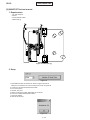
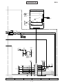
Figure 61 PWB repair jig
2. Setup
Figure 62
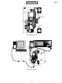
1. Set PWB and make connections as shown in Figures 64 and 65.
Make sure connections are correct at the points shown in Figure 66.
2. Connect PC and TQ-GX10i with Data Cable.
3. Turn on the phone.
4. Start RF Test Tool.
5. Select a COM port to which Data Cable is connected.
6. Press the “Initialize & Read Data” Button.
7. Figure 69 appears.
8. Click OK to proceed.
Figure 63
2 – 30
GX10i
CONFIDENTIAL
PWB
Setting Pin
Hook
Hook
Figure 64 PWB installation
Black
Red
PC
Data Cable
Figure 65 Connections
2 – 31
GX10i
CONFIDENTIAL
Point
Figure 66 Contact points
Push
Figure 67 Turning power on
2 – 32
GX10i
CONFIDENTIAL
3. Tests
3.1 BAND Select & Channel
Select a band and a channel to test. Settings are applied to all tests.
Input box
Band selection
Channel bar
Figure 68
[Procedure]
1. Select a band. (GSM or DCS)
2. Select or enter a channel using Channel bar or Input box.
3.2 TX test
Test burst transmission.
TX frequency of selected channels
Current PCL (Read only)
PCL bar
TX ON/OFF button
This indicator appears during
burst transmission.
Data patterns
Figure 69
[Procedure]
1. Select a band and channel. (see 3.1)
2. Select PCL (Power Control Level) using PCL bar.
3. Select Data pattern.
4. Click TX ON to start burst transmission.
(You can check each part in this state.)
5. Click TX OFF to end burst transmission.
* Data pattern (TSC 5) includes Training Sequence GSM 5, and other part is pseudo random data.
* There may be a slight difference between the power of burst transmission with this tool and that of actual calls. (approximately
0.1dB within PCS bandwidth.)
2 – 33
GX10i
CONFIDENTIAL
GX10i TX power Table (Target power during calibration, supply voltage: 3.7[V])
GSM
PCL
5
DCS
PCL
TX Power [dBm]
31.6
6
7
30.0
29.0
8
9
27.0
25.0
10
11
23.0
21.0
12
13
19.0
17.0
14
15
15.0
13.0
16
17
11.0
9.0
18
19
7.0
5.0
TX Power [dBm]
0
1
28.6
27.0
2
3
26.0
24.0
4
5
22.0
20.0
6
7
18.0
16.0
8
9
14.0
12.0
10
11
10.0
8.0
12
13
6.0
4.0
14
15
2.0
0.0
3.3 RX test
The phone receives burst signals in this test.
RX frequency of selected channels
Current RX Gain (Read only)
RX Gain Setting bar
RX ON/OFF button
This indicator appears while
receiving burst signals.
Sniff ON/OFF
Figure 70
[Procedure]
1. Select a channel and band. (see 3.1)
2. Select RX Gain using RX Gain Setting bar.
3. Choose Sniff ON or OFF.
4. Click RX ON to start receiving burst signals.
5. In continuous mode, transmit burst signals from GSM tester.
(You can check each part in this state.)
6. Click RX OFF to end receiving burst signals.
* In this test, the reception timing cannot be synchronized with burst signals from Signal Generator, etc.
* The standard RX Gain Setting is:
(Input power at the antenna connector of the phone) + (RX Gain) = –16 dBm
Excessive Input power or RX Gain may cause damage to the phone.
2 – 34
GX10i
CONFIDENTIAL
3.4 RSSI Measure
The phone notifies you of input power value at the antenna connector.
Measured power box
Estimated Power
Input box
(Integer only)
Measure button
Figure 71
[Procedure]
1. Connect the phone and GSM tester (or Signal Generator) with RF cable.
2. Select a band and channel. (see 3.1)
3. Send signals (*) from GSM tester.
4. Enter the value of input power from GSM tester in integers (from –10 to –110) considering RF cable loss.
5. Press the Measure button.
6. The result appears in Measured Power box.
* The signal type from GSM tester must be either of two:
1. Continuous sine wave (without modulation) with the frequency as follows:
(Frequency of the measured channel) + 67.708kHz.
(Ex. channel: GSM 37ch
the result: 942.467708 MHz)
Power: –110 to –10 dBm
2. BCCH signal of the measured channel
Power: –110 to –10 dBm
Result
When the phone is properly calibrated, the error between “Estimated Power” and “Measured Power” is less than 2dB.
4. Termination
Turn off the phone to ensure proper operations.
2 – 35
GX10i
CONFIDENTIAL
[3] Adjustment procedures after replacement of the parts
Be sure to make adjustments to the parts as shown in the table below.
1. Adjustment to
2. Adjustment to
camera temperature
battery temperature
3. Flicker adjustment 4. White defect 5. Optical axis
correction
adjustment
IC105
IC307
Camera FPC A’ssy
Main-screen Display
1. Adjustment procedures of camera temperature
1.
2.
3.
4.
5.
6.
7.
Place a thermometer near the unit to be adjusted. Make sure the room temperature is over 0°C.
Attach the battery pack.
Access the normal mode by holding down the power key.
Transmit the [AT+XDIAG] command.
Make sure the screen for the function test mode is displayed.
Access the TEMP ADJ mode by pressing the “ ” key, and push the “1” (1. CAM TEMP) key.
Temperature detected by the sensor is displayed after “Temp:”. Compare the displayed value to the room temperature.
Enter the difference as a corrected value with the “ ” key if the displayed value is higher, and use the “ ” key if it is lower.
The corrected value is displayed after “Correct:”.
8. Press the “#” key. [Param Save OK.] will be displayed to notify the corrected value is registed.
9. Press the “0” key to access the initial screen of the function test mode.
10. Press the “Power” key to exit this mode.
2. Adjustment procedures of battery temperature
1.
2.
3.
Perform steps 1 – 5 of “Camera temperature adjustment procedure”.
Access the TEMP ADJ mode by pressing the “ ” key, and push the “2” (2.BAT TEMP) key.
Perform steps 7 – 10 of “Camera temperature adjustment procedure”.
3. Flicker adjustment procedure
1.
2.
3.
4.
5.
Attach the battery pack.
Access the manual testmode
Access the manual testmodeF81 (LCD Setting) by pressing the “8”, “1” and “Right Soft” keys in this order.
Press the “2” (2. VCOM Adjust) key.
Adjust the flickers on the screen to the minimum by pressing the “ ” and the “ ” keys. Make sure visually they are minimized
at a distance of about 20 cm from the inverter fluorescent lamp. (Fine adjustments to the DC voltage between LCD
electrodes)
Enlargement
(Add a black line at every one line)
8 gradation patterns with a black line between each line of the patterns (monochrome pattern)
6.
7.
Press the “Centre” key twice. [Diag Param Saving] will be displayed to notify the corrected value is registered.
Press the “Power” key to exit this mode.
2 – 36
CONFIDENTIAL
GX10i
4. Procedures of white defect correction
1.
2.
3.
4.
5.
6.
Attach the battery pack.
Access the normal mode by holding down the power key.
Connect the unit to the PC and send the [AT+XDIAG] command.
Make sure the screen for the function test mode is displayed.
Send the [LDDEVPRM] command.
Block off light completely from the light sensor after receiving the [LDDEVPRMOK]. If the [LDDEVPRMNG] is received,
start from step 5.
7. Transmit the [WHC01540160] command.
8. 6 digits will be received if the transmission is completed after 20 to 30 seconds. Be sure to continue to block off light during
this process.
<6 digits to be received>
• In case of [LDDEVPRMOK]: aaabbb will be received.
aaa: the number of white defects
bbb: the maximum level of dark current
• In case of [LDDEVPRMNG]: 000000 will be received.
This indicates light was not blocked completely. Go back to step 7.
9. Send the [WH] command.
10. If [OK] is received, send the AT [SVDEVPRM] command.
11. After receiving the [SVDEVPRMOK], block off light completely from the light sensor. If the [SVDEVPRME1] is received,
go back to step 10.
12. Remove the Data cable from the unit. Press the “Power” key to exit.
* White defect correction
White defects indicate pixel defects in the image detected by the light sensor. These appear as white spots even when
light is completely blocked off (even on a black background). White defect correction solves this problem.
5. Optical axis adjustment
1.
2.
3.
4.
5.
6.
7.
8.
9.
Attach the battery pack.
Access the normal mode by holding down the “Power” key.
Connect the unit to the PC and send the [AT+XDIAG] command.
Make sure the screen for the function test mode is displayed.
Press the “6” key. The camera image will appear on the display.
Set your face in the center of the camera mirror and press the “Centre” key (for shooting). Correct the image with the “ ”
key if it is on the center right, and use the “ ” key if it is on the center left. Press the “Right Soft” key. [Param Save OK.]
will be displayed to notify the corrected value is registered. The screen is returned to the shooting screen. The image is
moved by 2 dots each time the “ ” or “ ” key is pressed.
Make sure the image is set in the center after performing step 6 several times.
Press the “0” key to access the initial screen of the function test mode.
Press the “Power” key to exit this mode.
2 – 37
GX10i
CONFIDENTIAL
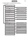
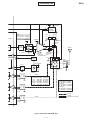
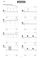
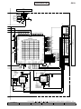
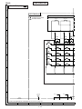
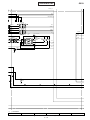
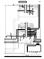
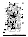
[4] Test points
Figure 72 TEST POINT
TP No.
Signal name
TP No.
Signal name
TP301
TP302
VSIM (2.85 V)
SIMCLK
TP312
TP313
TXD
ADP
TP303
TP304
SIMRST
SIMIO
TP314
TP315
BATT_SENSE
DGND
TP305
TP306
TDI
RXD
TP316
TP317
3V
VTCXO (2.9 V)
TP307
TP308
ADPDET
CONT2
TP319
TP321
VRF (2.9 V)
VBACK (3 V)
TP309
TP310
CONT1
RTS
TP324
TP344
MIC
D GND
TP311
CTS
TP345
KEY_BL_ON
2 – 38
TP306
TP312
TP302
TP303
TP324
TP323
TP345
TP315
TP322
TP313
TP310
TP308
TP309
TP305
TP311
TP307
TP304
TP316
TP321
TP301
TP314
TP319
TP317
TP344
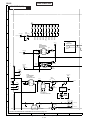
KEY PWB-B (FRONT SIDE)
GX10i
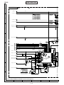
CONFIDENTIAL
TPB333
Figure 73 TEST POINT
TP No.
Signal name
TPB325 TXD
TPB326 RXD
TPB331 BATT_SENSE
TPB332 DGND
TPB333 BATT
TPB334 DGND
TPB335 BATT
TPB343 ADPDET
2 – 39
TPB343
TPB334
TPB335
TPB332
TPB331
TPB326
TPB325
TP342
TP329
TP330
TP328
KEY PWB-B (REAR SIDE)
GX10i
CONFIDENTIAL
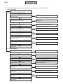
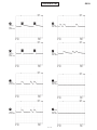
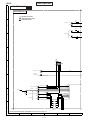
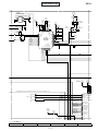
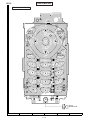
TP019
TP016
TP023
TP014
TP025
TP217
TP219
TP112
TP107
TP117
TP114
TP115
TP214
TP212
TP110 TP111
TP204
TP116
TP172
TP201
TP006
TP031
TP170
TP207 TP156
TP001
TP106
TP157
TP171
TP154
TP155
TP121
TP203
TP166
TP205
TP020
TP018 TP017
TP208
TP215
TP206
TP149
TP152 TP160
TP216
TP015 TP027
TP213
TP003
TP209
TP009
TP211
TP021
TP024
TP026
TP012
TP167
TP102
TP168
TP101
TP011
TP022
TP002
TP004
TP013
MAIN PWB-A (FRONT SIDE)
Figure 74 TEST POINT
TP No.
Signal name
TP No.
Signal name
TP No.
Signal name
TP001
/RD
TP026
GCS2
TP167
RECIVER_OUTP
TP002
TP003
/WR
/LCD_RST
TP027
TP031
GCS1
Back light (LED–)
TP168
TP170
RECIVER_OUTN
AUXADC2 (ADIN)
TP004
TP006
CS_TFTLCD
Back light (LED+)
TP106
TP107
JAKMIC
JAKEAR
TP171
TP172
AUXADC6
CLKOUTGATE
TP009
TP011
VDDCORE
13 MHzCLK
TP110
TP111
SP1
SP2
TP201
TP203
CHGIN
VBACK (3 V)
TP012
Terminal for LCDC adhesion
check 1
TP112
TP114
VVIB
TCK
TP204
TP205
BATT_SENSE
VRTC (1.8 V)
TP013
Terminal for LCDC adhesion
check 2
TP115
TP116
TMS
TDI
TP206
TP207
VCAM (3.1 V)
VCORE (1.8 V)
TP014
TP015
LCD 5 V
LCD 15 V
TP117
TP121
TDO
H_AMP
TP208
TP209
VANA (2.45 V)
VMEM (2.8 V)
TP016
TP017
LCD –10 V
LS
TP149
Terminal for STACK MEMORY
adhesion check 1
TP211
TP212
VLCD (2.5 V)
VEXT_CN (2.5 V)
TP018
TP019
DCLK
PS2
TP152
Terminal for STACK MEMORY
adhesion check 2
TP213
TP214
VINT (3 V)
VINT_SW (3 V)
TP020
TP021
PS1
SPL
TP154
TP155
TMS/CHECKER_1
TCK_/LED_ON
TP215
TP216
VT (2.715 V)
VIR (2.8 V)
TP022
TP023
GSP
GCK
TP156
TP157
EXT1
CLKOUT
TP217
TP219
POWONKEY
VBAT_BB
TP024
TP025
ALW
GMODE
TP160
TP166
Flash-Vpp
CINT
2 – 40
GX10i
CONFIDENTIAL
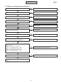
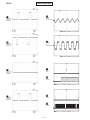
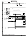
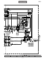
TP126
TPB008
TPB162
TP118
TP144
TP138
TP146 TP147
TP137
TP125
TP148
TPB007
TPB220
TPB218
TPB165
TP124
Figure 75 TEST POINT
TP No.
Signal name
TPB162 TCK/LED_ON
TPB163 TDI
TPB164 TDO
TPB165 TMS_CHECKER
TPB169 JTAG (3VINPUT)
TPB218 POWONKEY
TPB220 POWONKEY
2 – 41
TPB164
TP141
TP123
TP132
TP131
TP139
TP129
TP150
TPB163
TPB169
TP158
TP128
TP176 TP180 TP178
TP174 TP175 TP179
TP173 TP177
TP151
TP153
TP130
TP122
TP127 TP133
TP145
TP134
MAIN PWB-A (REAR SIDE)
GX10i
CONFIDENTIAL
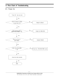
[5] Troubleshooting
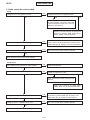
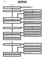
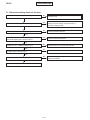
1. Power does not turn on.
Connect a battery with voltage of more than 4.0 V.
NOTE: If the cause is damage to 4-level memory (IC106), ensure
to upload flash data before operation as initializing user
area may prevent detecting the damaged data.
NO
Manual test mode gained?
A
YES
Can initialization of only user area (File System) be
conducted by Flash Loader?
NO
4-level stack memory (IC106), and IC104 defective.
YES
YES
Does the normal mode start?
4-level stack memory (IC106) data damaged.
NO
NO
Is the program rewritable?
4-level stack memory (IC106), and IC104 defective.
YES
After restart, the normal mode gained?
YES
Program of 4-level stack memory (IC106) transformed.
NO
4-level stack memory (IC106), and IC104 defective.
A
More than 3.6 V output at Battery terminal (TPB333,
TPB335)?
NO
Battery terminal defective, adhesive foreign matter at
contact battery (CN303) terminal, or bad soldering.
YES
Voltage of below 1.6 V applied to SENSE terminal
(TPB331 or TP314)?
NO
Battery or battery mounting defective.
YES
NO
Is fuse (FS302) connected?
Blowout of fuse (FS302).
YES
More than 3.6 V output at VBAT_BB terminal (TP219).
NO
Relay FPC_A or connector CN201 defective.
YES
Voltage of below 1.6 V applied to SENSE terminal (C187
signal side)?
NO
Relay FPC_A or connector CN201 defective.
YES
Is 4-level stack memory (IC106) properly mounted?
NO
Defective mounting of 4-level stack memory (IC106).
YES
2.8 V output at VMEM (TP209), and 1.8 V output at
VCORE (TP207), respectively?
NO
Power supply IC (IC202) defective.
YES
32.768 kHz properly output at X101 2 pin?
NO
X101(32 kHz oscillator), and oscillation circuit defective.
YES
13 MHz properly output at TP011?
YES
IC104 defective.
NO
2.9 V output at VTCXO (TP317)?
NO
Regulator (IC303) defective.
YES
TCXO (TCX951), IC901 and peripheral circuit defective.
2 – 42
CONFIDENTIAL
GX10i
2. Incoming audio cannot be heard.
Phone
Signal output at TP167/TP168?
YES
Built-in receiver defective or defective connection between
TP167 and TP168.
NO
YES
Signal output at C102?
L103 or L104 defective.
NO
YES
Signal output at C120?
L103 to IC102 62pin, L104 to IC102 61pin, L103, L104,
L107, and L108 defective.
NO
Voltage of more than 0.5 V applied to C186 (IC102 6 pin
side) ?
YES
IC102 or PWB defective.
NO
Voltage of more than 2.4 V applied to Q101 3 pin?
YES
Relay FPC_B, CN202, CN306, JK301, R106, and R109
defective.
YES
Hands free kit defective.
NO
Q101, Q101 2 pin to IC104 78 pin, and IC104 defective.
Hands free kit
When replacing the hands free kit, output available?
NO
YES
Signal output at JK301 4 pin?
Defective connection of JK301.
NO
YES
Signal output at TP107?
Relay FPC_B, CN202, CN306, L303, and JK301 defective.
NO
YES
Signal output at C117?
C104 defective.
NO
Is the voltage of 0 V applied to C186?
YES
NO
Relay FPC_B, CN202, CN306, and JK301 defective.
2 – 43
IC102 or PWB defective.
GX10i
CONFIDENTIAL
3. Audio cannot be sent/recorded.
Phone
Voltage of 0.5 to 1.5 V applied to TP324?
YES
NO
Voltage of more than 0.5 V applied to C186?
YES
NO
Built-in microphone defective. Defective
connection between microphone and PWB.
Components between IC102 54 pin and L314
defective. IC102 defective.
Defective connection between IC102 6pin and
JK301 5 pin difective. JK301, Relay FPC_B,
CN202, CN306, and R109 defective.
Voltage of 0.5 to 1.5 V applied to R112 (C185 side)?
YES
NO
Voltage of more than 2.4 V applied to Q101 3 pin?
YES
Defective connection between jumper (IC102 54 pin to
C101) to L314 or jumper (CN202 9 pin to earth) to L315.
CN202, Relay FPC_B, CN306, L314, and L315 defective.
Q101 3 pin to R112, R106, and R112 defective.
NO
Q101 and Q101 2 pin to IC104 78 pin defective.
Hands free kit
When replacing the hands free kit, output avilable?
YES
Hands free kit defective.
NO
Voltage of 0.5 to 1.5 V applied to C306?
YES
NO
Voltage of 0 V applied to C186?
YES
NO
JK301, IC102 44 pin to L303, IC102, and L105
defective.
JK301 5 pin to IC102 6 pin, JK301, R366,
CN306, Relay FPC_B and CN202 defective.
Voltage of 0.5 to 1.5 V applied to TP106?
YES
NO
Voltage of over 2.4 V applied to Q101 3 pin?
YES
NO
Q101 and Q101 2 pin to IC104 78 pin defective.
2 – 44
Defective connection between jumper (C103 to CN202 18
pin) to L303 or jumper (CN202 9 pin to earth) to L105.
CN202, Relay FPC_B, CN306, and L303 defective.
Q101 3 pin to R109, R106, and R109 defective.
GX10i
CONFIDENTIAL
4. Charging impossible.
Start the test mode, using a batterry fully charged with a
specified battery charger. Check that the battery voltage is
more than 4.15 V.
Is the voltage of 3 V applied to TP156 when Charge LED
is ON?
YES
Does “ChargeLED” turn on/off when press “1” key by
manual testmode F45 (LED setting)?
Q103, R129, and
LED101 defective.
NO
NO
Defective connection between
IC104 88 pin and Q103 Base.
IC104 Defective.
YES
Is the temperature shown in the procedure "2.BAT TEMP"
of manual testmode F42 (Temp Adjust) correct? (Measuring
tolerance: _
+ 5 deg)
NO
IC307, R368, CN305, Relay FPC_B, CN201, and IC102
defective.
NO
Defective connection between IC202 5 pin and IC102 4 pin.
IC102 and IC202 defective.
YES
Is the battery voltage of 4.15 to 4.25 V shown in the
procedure manual testmode F80 (Voltage control)?
YES
Startup in the normal mode, using a battery with the voltage
of 3.3 to 3.8 V.
When insering AC Charger in External Connector, is the
voltage of approx. 5.2 V applied to TP201?
NO
Defective connection between CN302 18 pin and IC202 7
pin.
CN302, CN306, FL303, FL304, FL307, Relay FPC_B, and
CN202 defective.
YES
Approx. 3 to 15 sec after inserting AC Charger in External
Connector, does the voltage of TPB335 increase by more
than 0.05 V?
NO
YES
Battery defective.
2 – 45
Defective connection between IC202 9 pin and Q305 3 pin.
CN305, Relay FPC_A, CN201, R348, Q305, D303, and
IC202 defective.
GX10i
CONFIDENTIAL
5. Vibrator does not operate.
Do the vibrator terminals contact with the land?
NO
Vibrator defective.
YES
Does the voltage between the vibrator terminals show
more than 3 V?
YES
Vibrator defective.
NO
Does the voltage of TP112 show more than 3 V?
YES
CN201 or Relay FPC_A, CN305, breaking defective.
NO
VBAT_AP Voltage applied to IC105 5 pin?
YES
IC101 defective.
NO
VBAT_AP Voltage applied to CN201 21 pin?
NO
CN201 or Relay FPC_A, CN305, breaking defective.
YES
Signal output from IC103 19 pin?
YES
IC101 defective.
NO
Voltage of approx. 3 V applied to IC103 7 pin?
NO
Jumper (IC103 7 pin to VINT LINE) defective.
YES
IC103 or the control signal line to IC104 defective.
6. Clock is reset.
More than 2.5 V output at TP316 when a back-up battery
is fitted in the set?
NO
Regulator IC302 defective.
YES
More than 2.5 V output at TP321 when a back-up battery
is fitted in the set?
NO
Voltage detecter IC305 or Q307 and Q306 defective.
YES
Defective mounting of back-up battery holder.
NO
More than 1.5 V output at TP321 when a back-up battery
is not fitted in the set?
NO
Is the back-up battery holder properly mounted?
YES
YES
• Insufficient back-up battery capacity.
• Back-up battery defective.
• Back-up battery holder defective.
More than 1.5 V output at TP203 when a back-up battery
is not fitted in the set?
NO
Relay FPC_B or fastening connector defective.
YES
More than 1.2 V output at TP205 when a back-up battery
is not fitted in the set?
NO
YES
IC104 defective.
2 – 46
Regulator IC203 defective.
GX10i
CONFIDENTIAL
7. Speaker does not operate.
*When ring tones sound but only key touch tones do not, "Keypad Tones" are set to OFF.
Do speaker terminals contact with the land?
NO
Speaker defective.
YES
Resistance of 8 ohms available between the speaker
terminals?
NO
Speaker defective.
YES
Signal output at the speaker land on the relay FPC?
YES
Speaker defective.
NO
Signal output at TP110/TP111 ?
YES
CN201 Defective or Relay FPC_A breaking defective.
NO
YES
VBAT_AP Voltage applied to IC103 15pin?
NO
VBAT_AP Voltage applied to CN201 21 pin?
NO
Relay FPC_A, CN305, and CN201 defective.
YES
Voltage of approx. 3 V applied to IC103 7 pin?
NO
R507 and Jumper (IC103 7 pin to VINT LINE) defective.
YES
Signal output at IC103 12 pin?
YES
R122 and R123 defective.
NO
IC103 defective or control signal line to IC104 defective.
8. Back light does not turn on.
Do the keypad tones and ring tone sound from the speaker?
NO
Jumper (between FS302 and CN305 12 pin) or Relay
FPC_A, CN305, CN201 defective.
YES
Voltage of VBAT_AP applied between CN201 21 pin and
FS001?
NO
Jumper (between CN201 21 pin and FS001) defective.
YES
Defective mounting or blowout of FS001.
NO
Voltage of VBAT_AP applied to IC001 6 pin?
NO
Is FS001 (Fuse) properly mounted or connected?
YES
YES
C027 and C003 defective.
To the next page
2 – 47
GX10i
CONFIDENTIAL
From the previous page
Which display does not light up? Main or sub?
Only sub-screen display back light.
A
Only main-screen display back
light or both displays’ back lights.
Is the main-screen display back light set to ON?
NO
ON Setting by the following menu.
Settings
Phone settings
Back light
YES
NO
Does the back light turn on?
YES
Nondefective.
Is the back light FPC properly soldered at the soldering
terminals?
NO
Back light FPC soldering defective.
YES
Voltage of 13 to 24 V applied between the back light FPC
soldering terminals?
YES
Back light FPC or LED defective.
NO
IC104 or Jumper (between IC104 33 pin and IC001 4 pin)
defective.
NO
Is the standby back light turned on?
NO
Is the pulse shape sent to IC001 4 pin? (Don’t hold to Low?)
YES
YES
IC001, L001, D001 and L003 defective.
Voltage of 3 V applied to Q001 gate (G) terminal?
NO
IC104 defective.
YES
Voltage of less than 10 mV applied to Q001 drain (D) (R001
side) terminal?
NO
Q001 defective. (approx. 95 mV at drain terminal)
YES
R001, R003 and IC001 defective.
A
Is the sub-screen display back light set to ON?
NO
ON Setting by the following menu.
Settings Phone settings
External display
Back light
YES
NO
Does the back light turn on?
YES
Nondefective.
Voltage of 3 V applied to Q002 gate (G) terminal?
NO
YES
LED001 or Q002 defective.
2 – 48
Defective connection between IC104 64 pin and Q002
gate (G) or IC104 defective.
CONFIDENTIAL
GX10i
9. "No Service" display and receiving/transmitting do not function.
9. 1 "No Service" display and receiving/transmitting do not function in the EGSM band.
[Receiving System]
YES
Does the signal strength indicator show 4 bars?
* Fixed line: During input of –70 dBm.
NO
After replacing the main PWB unit with a normal one,
receiving available?
YES
IC104, IC102, CN201, CN202, or PWB defective.
NO
After replacing FPC (flexible printed circuit) with a
normal one, receiving available?
YES
FPC defective.
NO
NO
Voltage applied to VCO971 7 pin?
IC202, IC303, Q304, or Q308 defective.
YES
Is VCO971 frequency fixed at 4 times as the EGSM
band receiving frequency?
NO
IC901, VCO971, FL971, TCX951, or IC304 defective.
YES
EGSM-Band Receiving frequency signal applied to
IC901 10 and 11 pins?
YES
IC104, IC102, IC901, or PWB defective.
NO
EGSM-Band Receiving frequency signal output from
FL801 7 pin?
YES
FL901 defective.
NO
EGSM-Band Receiving frequency signal input to
FL801 9 pin?
YES
IC991, IC992, IC993, or FL801 defective.
NO
J801 defective.
[Transmitting System]
NO
Voltage applied to VCO971 7 pin?
IC202, IC303, Q304, or Q308 defective.
YES
Is VCO971 frequency fixed at 4 times as the EGSMband transmitting frequency + 80 MHz (or 82 MHz)?
NO
IC901, VCO971, FL971, TCX951, or IC304 defective.
YES
IQ Signal input to IC901 20, 21, 22, and 23 pins?
NO
IC104, IC102, or PWB defective.
NO
Q304 or Q309 defective.
NO
VCO851, IC901, IC991, IC992, or IC993 defective.
YES
Voltage applied to VCO851 11 pin?
YES
EGSM-Band Transmitting frequency input to IC831 1 pin?
YES
EGSM-Band Transmitting frequency input to FL801 11 pin?
NO
FL811, R811, IC881, or IC831 defective.
YES
EGSM-Band Transmitting frequency input to J801 1 pin?
YES
J801 defective.
2 – 49
NO
FL801 defective.
GX10i
CONFIDENTIAL
9. 2 "No Service" display and receiving/transmitting do not function in the DCS (PCS) band.
[Receiving System]
YES
Does the signal strength indicator show 4 bars?
* Fixed line: During input of –70 dBm.
NO
After replacing the main PWB unit with a normal one,
receiving available?
YES
IC104, IC105, CN201, CN202, or PWB defective.
NO
After replacing FPC (flexible printed circuit) with a
normal one, receiving available?
YES
FPC defective.
NO
NO
Voltage applied to VCO971 7 pin?
IC202, IC303, Q304, or Q308 defective.
YES
Is VCO971 frequency fixed at twice as the DCS
(PCS) band receiving frequency?
NO
IC901, VCO971, FL971, TCX951, or IC304 defective.
YES
DCS (PCS)-Band Receiving frequency signal applied
to IC901 7 and 8 (4 and 5) pins?
YES
IC104, IC102, IC901, or PWB defective.
NO
DCS (PCS)-Band Receiving frequency signal output
from FL801 5 (3) pin?
YES
FL902 (FL903) defective.
NO
DCS (PCS)-Band Receiving frequency signal input
to FL801 9 pin?
YES
IC991, IC992, IC993, or FL801 defective.
NO
J801 defective.
[Transmitting System]
NO
Voltage applied to VCO971 7 pin?
IC202, IC303, Q304, or Q308 defective.
YES
Is VCO971 frequency fixed at twice as the DCS (PCS)band transmitting frequency + 80 MHz (or 82 MHz)?
NO
IC901, VCO971, FL971, TCX951, or IC304 defective.
YES
IQ Signal input to IC901 20, 21, 22, and 23 pins?
NO
IC104, IC102, or PWB defective.
NO
Q304 or Q309 defective.
YES
Voltage applied to VCO851 11 pin?
YES
DCS (PCS)-Band Transmitting frequency input to
IC831 8 pin?
NO
VCO851, IC901, IC991, IC992, or IC993 defective.
YES
DCS (PCS)-Band Transmitting frequency input to
FL801 1 pin?
NO
FL816, R816, IC881, or IC831 defective.
YES
DCS (PCS)-Band Transmitting frequency input to
J801 1 pin?
YES
J801 defective.
2 – 50
NO
FL801 defective.
CONFIDENTIAL
GX10i
10. Main-screen display does not function.
Does the display function after replacement?
YES
Main-screen display defective.
NO
More than 3.2 V applied to TP219?
NO
Refer to Troubleshooting, “Power does not turn on.”
(see page 2-42)
NO
Refer to Troubleshooting, “Power does not turn on.”
(see page 2-42)
YES
More than 2.8 V ±0.1 V applied to TP209?
YES
More than 2.5 V ±0.1 V applied to TP009?
NO
Regulator IC004 defective.
YES
13 MHz output at Clock TP011?
NO
Refer to Troubleshooting, “Power does not turn on.”
(see page 2-42)
YES
0.1V output at both ends of the liquid crystall reset (Jumper
(IC005 40 pin to Q206 2 pin))?
NO
IC004 Defective.
YES
3.0 V ±0.1 V output at IC002 7 pin?
NO
IC005 Defective.
YES
-10.2 V ±0.6 V output at TP016, 15.3 V ±0.9 V at TP015,
and 5.1 V ±0.1 V at TP014, respectively?
NO
Charge pump regulator IC (IC002) defective.
YES
Are amplitude waveforms of IC003 terminals normal as
shown below?
18 pin: 2.7 Vpp (offset value 0V)
17 pin: 1.12 Vpp (offset value -0.06 V)
16 pin: 0.24 Vpp (offset value -0.07 V)
15 pin: 0.78 Vpp (offset value -0.10 V)
14 pin: 2.86 Vpp (offset value -0.14 V)
NO
Grayscale generator IC (IC003) defective.
YES
Does output of TP017 to TP027 have pulse waveforms?
NO
YES
Display defective. Or defective mounting of connector
CN002.
2 – 51
IC005 Defective.
GX10i
CONFIDENTIAL
11. Sub-screen display does not function.
Does the main-screen display function?
NO
Refer to Troubleshooting, “Power does not turn on.”
(see page 2-42)
YES
Is the sub-screen display set to ON?
NO
ON Setting by the following menu:
Settings ––> Phone settings ––> External display ––>
Sub-screen display On/Off.
YES
Is PWB connector CN001 surely inserted?
NO
Connector insertion defective.
YES
Clean the connector CN001 contact point and insert the
sub-screen display again. Does it function?
YES
Connector insertion part soiled.
NO
Voltage of 3 ±0.1 V applied to CN001 7 pin?
NO
Jumper (CN001 7 pin to VINT Line) defective.
YES
NO
Is CN001 5 pin on the high level?
Jumper (CN001 5 pin to Q206 2 pin) defective.
YES
Voltage of approx 6.4 V applied to CN001 8 pin?
NO
YES
Sub-screen display unit defective.
2 – 52
C017, control signal line to IC104, or the sub-screen
display unit defective.
GX10i
CONFIDENTIAL
12. Camera does not function.
Voltage of 2.5 V applied to TP211?
NO
Regulator IC201 and jumper (IC201 5 pin to Q205 emitter)
defective.
NO
Jumper (CN101 10 pin to VLCD Line) and CN101 defective.
Defective disconnection of camera FPC Ass’y .
YES
Voltage of 2.5 V applied to camera module (CA1001)
36 pin?
YES
IC104 defective.
NO
Voltage of 3.0 V applied to TP214?
NO
Voltage of 3.0 V applied to Q206 2 pin?
YES
YES
FET Q206 defective
Voltage of 3.0 V applied to camera module (CA1001)
18 pin?
NO
Jumper (CN101 7 pin to Q206 3 pin) and CN101 defective.
Defective disconnection of camera FPC A’ssy.
YES
IC104 defective.
NO
Voltage of 3.1 V applied to TP206?
NO
Voltage of 3.0 V applied to IC206 1 pin?
YES
YES
Regulator IC206 defective.
Voltage of 3.1 V applied to camera module (CA1001)
8 pin?
NO
Jumper (CN101 33 pin to IC206 4 pin) and CN101 defective.
Defective disconnection of camera FPC A’ssy.
YES
Is duty of the 13 MHz Clock (TP157) within the range of
40% to 60%?
NO
IC104 defective
YES
Are access signals (R159 both ends) to camera module
rectangular waves?
NO
IC104 defective
YES
Are interrupt signals (TP166) from camera module
rectangular waves?
NO
YES
IC104 or camera module defective.
2 – 53
Camera module defective.
GX10i
CONFIDENTIAL
13. SIM Card is not recognized.
Can SIM card be recognized after replacement?
NO
SIM card defective or undesignated SIM card used.
YES
NO
2.8 V Output at Q208 5 pin?
IC104 defective.
YES
2.85 V Output at SIM power supply IC202 18 pin?
NO
IC202 or Q208 defective.
YES
Do Jumper (IC104 95 pin to CN201 27 pin) and Jumper
(IC104 102 pin to CN201 28 pin)regularly output pulse
waves?
NO
IC104 defective.
YES
Does TP301 (SIM power source) output 2.85 V?
NO
YES
Do TP304 and TP302 regularly output pulse waves?
NO
YES
Does SIM reset signal TP303 output 3.0 V?
NO
Defective parts between IC202 18 pin to CN301 1 pin,
CN202, Relay FPC_B, CN306 and jumper (CN301 1 pin to
CN306 13 pin) defective.
Defective parts between IC104 95 pin to CN301 6 pin or
IC104 102 pin to CN301 3 pin. CN201, Relay FPC_A,
CN305 and jumper (CN301 6 pin to R305) defective.
Defective parts between IC104 114 pin to CN301 2 pin,
IC104, CN201, Relay FPC_A, CN305 and R363 defective.
YES
Is SIM card connector (CN301) properly mounted?
NO
YES
IC104 defective.
2 – 54
Defective mounting of SIM card connector (CN301).
CONFIDENTIAL
GX10i
14. IrDA Communications unavailable
Set the specified distance and angle necessary for IrDA
communications.
NO
2.8 V Output at Q207 2 pin?
IC104 defective.
YES
Does IrDA power source TP216 output 2.8 V?
NO
Q207 defective.
YES
Do transmitting signals (R142 signal side) regularly output
pulse waves?
NO
IC104 defective.
YES
3.0 V Output at VCC (UN301 3 pin)?
NO
Defective parts between IC205 5 pin to UN301 3 pin.
CN202, Relay FPC_B, CN306 and jumper (UN301 3 pin to
R354) defective.
YES
More than 2.0 V available for IrDA power source (UN301 8
pin)?
NO
Defective parts between Q207 3 pin to UN301 8 pin.
CN202, Relay FPC_B, CN306 defective.
NO
Defective parts between UN301 5 pin to Q207 6 pin.CN305,
Relay FPC_A, CN201 defective.
NO
Defective connection between UN301 6 pin to IC104 52
pin. CN201, Relay FPC_A, CN305 defective.
NO
Defective parts between IC104 39 pin to UN301 7 pin.
CN201, Relay FPC_A, CN305 defective.
YES
Less than 0.2 V applied at SD signal (UN301 5 pin)?
YES
Do receiving signals (UN301 6 pin) regularly output pulse
waves?
YES
Do transmitting signals (UN301 7 pin) regularly output
pulse waves?
YES
After replacement of Infrared port (UN301), communications
available?
NO
YES
Infrared port (UN301) defective or defctive mounting.
2 – 55
IC104 defective.
GX10i
CONFIDENTIAL
[6] Specification for function test
Outline
AT commands are used for the function test mode.
To enter the general mode, send the command “AT+XDIAG”.
Then the machine can accept all key test functions (see “All Key Test and Others” on page 2-70) and further commands from
the computer.
KEY Layout
Left Soft
Right Soft
Side
Up
Centre
Side
Down
Send
End/Power
1
2
ABC
3
DEF
4
GHI
5
JKL
6
MNO
7
PQRS
8
TUV
9
WXYZ
0
#
Logic of signals
1) Setting function (AT Command: AT+XDIAG)
Asynchronous (Consisting of 115200bps, data length 8, start 1, stop 1, and Parity None).
2) After shifting to Function Test
Incoming/Outgoing serial signals should be as follows.
ST
ST:
D0-D7:
PB:
SP:
D0
D1
D2
D3
D4
D5
D6
D7
PB
SP
H
L
Start bit
Data bit
Parity bit
Stop bit
After AT+XDIAG
1. Transmission rate: 19,200bps
2. Synchro system
Asynchronous (Consisting of data length 8, start 1, stop 1, and Parity None)
Signal protocol
1. The personal computer requests a response from a mobile machine to establish communications.
2. When keys are pressed, appropriate key codes are transmitted serially.
3. ASCII Characters (only capitals in the case of alphabet) are used for incoming/outgoing serial signals. At the end, return
codes (0Dh, 0Ah) are added.
4. Once making a request, the personal computer cannot make another request until the mobile machine returns a certain
response. Time-out does not occur.
2 – 56
CONFIDENTIAL
Basic procedure (when using Hyper terminal)
Flow chart
Connect the phone to PC.
Turn on the phone.
Open Hyper terminal.
Send “AT+XDIAG” with 115200 bps and proper “ASCII setting”.
The phone is in the All key test mode.
Change the baud rate from 115200 bps to 19200 bps for further commands.
Send further commands to check the phone.
2 – 57
GX10i
GX10i
CONFIDENTIAL
(Details)
1. Connect the phone to the computer via a data cable.
2. Turn on the phone.
3. Open Hyper terminal. (Start Program Accessory Communication
4. Enter the name and choose the desired icon. Then click “OK”.
Figure 76
5. Choose the appropriate COM port for network and click “OK”.
Figure 77
2 – 58
Hyper terminal)
CONFIDENTIAL
6. Adjust the port settings and click “OK”.
Figure 78
7. From the file menu, select “Properties” and click the Settings tab.
Figure 79
2 – 59
GX10i
GX10i
CONFIDENTIAL
8. Click “ASCII setting” and check “Send line ends with line feeds” and “Echo typed characters locally”.
Figure 80
9. Click “OK” for “ASCII setting” and “Properties” to exit.
Figure 81
2 – 60
CONFIDENTIAL
GX10i
10. Send “AT+XDIAG”
• You will see AATT++XXDDIIAAGG instead of AT+XDIAG as shown below by the Local echo mode, although you input
AT+XDIAG.
• After sending you will receive “OK”, and the machine should enter the All key test mode (see “All Key Test and Others”
on page 2-70).
Figure 82
11. If you send further commands, you must change the baud rate from 115200 to 19200 as follows;
11-1. Disconnect communications.
Clik here
Figure 83
2 – 61
GX10i
CONFIDENTIAL
11-2. From the file menu, select “Properties” and click “Configure...”.
Then change the baud rate to 19200 as follows;
Clik here
Figure 84
11-3. Click “OK” for “Port setting” and “Properties” to exit.
You can now send commands. (See example below for the “BATVAL” command.)
Figure 85
2 – 62
GX10i
CONFIDENTIAL
1) Basic Operation Test
<Startup and initial condition>
Fit a battery or a dummy battery in the set. Hold down the “End/Power” key to start up in the general mode. Then enter
AT+XDIAG without pressing any key. Start up in the general function test mode. (3 sec. until startup)
Back light OFF
After startup, “H/W CHECK ∗ GX-10i ∗” is displayed.
When adjusting by the AT command, be sure to perform the LDDEVPRM command before adjustment and the SVDEVPRM
command after adjustment.
Incoming/Outgoing Serial Signal Format for Basic Operation Test
Item
FROM to
SRAM
Incoming Serial Signal Outgoing Serial Signal
Command
LDDEVPR
M
LED
Checking
LCD back
light voltage
Contents
Test Method
n
Response
None
LDDEVPRM OK
LDDEVPRM NG
5
4
3
2
1
LEDn (n=0, 1, 2, 3, 4) Sub-screen display back light.
Key back light LED.
Red LED lights up.
Green LED lights up.
Main-screen display back light
lights up.
All LEDs light off. *1
Checking that LEDs light up.
LED1: Main-screen display
back light lights up.
LED2: Green LED lights up.
LED3: Red LED lights up.
LED4: Key back light lights up.
LED0: All LEDs light off.
0
FROM to SRAM extension.
Before adjustment perform this
The contents of FROM are dam- command to output the adjustment
aged.
value stored in FROM to SRAM.
Measuring
RTC clock
OUT32K
1
0
OUT32Kn
32 kHz Output (MON Output)
32 kHz Stop (Returned to
ALT1)
Checking frequency of the real time
clock.
Normal: When OUT32K1 is transmitted,
TP205 frequency is 32.768 kHz ±1.11
kHz.
Battery
voltage
check
BATVAL
None
Okn.nn
Reading down to the last two
digits of voltage.
Reading the voltage of the battery
power line. BATVAL is transmitted,
“OK” and the voltage value are
returned.
RTC Test
(Writing)
RTCWR
yymm
ddhh
mmss
OK
Writing time of day
“yymmddhhmmss” to RTC. *2
Writing time to the clock.
When RTCWR yymmddhhmmss is
transmitted, yy (year), mm (month),
mm (hour), and ss (minute) are written.
RTC Test
(Reading)
RTCRD
None
RTC yymmddhhmmss Reading time of day
“yymmddhhmmss” from RTC.
*2
Reading time of the clock. When
RTCRD is transmitted, time of day is
read out.
4
3
ADSETOK
TMPADH <Readout
AD value>
TMPADL <Readout AD
value>
TMPADRDY
Refer to the “Adjustment procedures
after replacement of parts” on pages
2 – 36 and 2 – 37.
Temperature TMPAD
A/D
Adjustment
2
1
Temperature TMP
check
n
Adjustment mode ended. *3
2.2 V Measurement started.
0.4 V Measurement started.
Adjustment mode started.
TMPnxx: Temperature Temperature readout. (0 ˚C
NG: Except 0 – 50 ˚C min.)
n=1: Camera
n=2: Battery
2 – 63
Reading temperature measured by
the temperature sensor.
When TMP is transmitted, TM and
temperature are returned. In case of
other than 0 – 50 ˚C, “NG” is returned.
GX10i
CONFIDENTIAL
Item
Incoming Serial Signal Outgoing Serial Signal
Command
Temperature TMPADJ
correction
IrDA Test
IRDA
n
4nn
TMPADJ4nn
3nn
TMPADJ3nn
2nn
TMPADJ2nn
1nn
TMPADJ1nn
1
2
3
4
5
6
OK
NG aa
NG NODATA
IrDA Jig
Mode
IRDACH
1
2
3
4
5
6
OK
(Vibrator)
VIB
Memory test MEMCHK1
(SRAM)
Memory test MEMCHK2
(PSRAM)
Battery side -nn ºC. (Not cumulative subtraction)
Battery side +nn ºC. (Not cumulative addition)
Camera side -nn ºC. (Not cumulative subtraction)
Camera side +nn ºC. (Not cumulative addition)
“nn”: To input difference from
the present temperature.
Cumulative addition is
unavailable for more than one
transmission.
Correcting difference between the
ambient temperature and the
temperature read by the sensor.
Comparing the ambient temperature
and the temperature read by the
sensor to transmit the corrected
value.
TMPADJ15: To raise temperature by
5 °C.
TMPADJ25: To reduce temperature
by 5 °C.
* When the same commands are
transmitted several times, corrected vales are not added.
1: 2.4 kbps
2: 9.6 kbps
3: 19.2 kbps
4: 38.4 kbps
5: 57.6 kbps
6: 115.2 kbps
“OK” if “5A” is detected.
If values other than “5A” are
detected, they are returned.
Data cannot be received.
Provide the set in the IrDA jig mode
to the other end of the line to perform the transmitting/receiving test.
When IRDA is transmitted, the set in
the IrDA jig mode receives signals
and returns “5A”. Detecting “5A”, the
tested set returns “OK” to the personal computer.
When values are other than “5A”,
Ngaa is returned. If data cannot be
received, NG NODATA is returned.
*4
1: 2.4 kbps
2: 9.6 kbps
3: 19.2 kbps
4: 38.4 kbps
5: 57.6 kbps
6: 115.2 kbps
IrDA Jig mode entered.
After that commands are
rejected.
When IRDACH5 is transmitted, using
the command to set the IrDA jig
mode, the jig mode starts.
Reset, or disconnect the power from
the set, to release the jig mode. *4
Asynchronous drive. (Always Checking vibrator operation.
When VIB1 is transmitted, the vibrator
ON)
operates continuously; when VIB2 is
Stop.
transmitted, it stops operation.
1
0
MELOn
Melody playback.
Stop. *5
00000
00000
07FF
FE5
MEMCHK1 OK
Checking read/write of 4Mbit SRAM.
Addresses (00000000 to
0007FFFE) are checked.
For NG, the address
“00000000” and the readout
data “dddd” are returned.
(dddd: Production Process No)
00300
00000
3FFF
FE5
MEMCHK2 OK
0
MELO
Test Method
VIBn
1
MA2 Test
(Sound)
Contents
Response
MEMCHK1 NG 0000
0000dddd
MEMCHK2 NG 0030
0000dddd
Checking melody playback.
When MELO1 is transmitted, melody
is played back from the speaker;
when MELO2 is transmitted,
playback stops.
Checking read/write of 16 Mbit.
Addresses (00300000 to 003
Smartcombo RAM.
FFFFE) are checked.
For NG, the address
“00300000” and the readout
data “dddd” are returned.
(dddd: Production Process No)
2 – 64
GX10i
CONFIDENTIAL
Incoming Serial Signal Outgoing Serial Signal
Item
Command
SRAM to
FROM
saving
n
SVDEVPRM None SVDEVPRM OK
SVDEVPRM E1
POWER OFF PWRDOWN
Contents
Response
None None
Test Method
After adjustment, adjusted values in
SRAM to FROM saving.
Garbled SRAM (No saving).*6 SRAM are saved to FROM.
POWER OFF
POWER OFF when PWRDOWN is
transmitted.
*1: The LED test is also available in the manual test mode F45.
<Startup>
1. Fit a battery in the set to start the manual test mode.
2. Press the keys “4”
“5”
“Right Soft” to start the manual test mode F45 (LED Setting).
3. Press the following keys for ON/OFF operation.
Key
Description
Contents
“0”
OFF
All switches OFF
“1”
Charge LED ON/OFF
Charge LED (LED101: RED)
“2”
Incoming call LED ON/OFF
MA2 LED (LED101: GREEN)
“3”
Key LED ON/OFF
Key LED (LED302 to LED309: GREEN)
“4”
Back light ON/OFF
LCD Back light (Back light FPC: WHITE)
“5”
Test LED ON/OFF
Test LED (Not mount)
“6”
Sub back light ON/OFF
Sub Back light (LED001: WHITE)
“Centre”
End
Shifting from this mode to the initial screen
Every time a key is
pressed, the
operation, “OFF
Brightness 1
2
3
4
standby
light”, is repeated.
4. Press the key “Centre” to return to the initial screen with the display, “Diag Param Saving”.
5. Press the “End/Power” key to finish operation.
*2: YY=00: Year of 2000
RTC writing is also available in the manual test mode F40.
<Startup>
1. Fit a battery in the set to start the manual test mode.
2. Press the keys, “4”
“0”
“Right Soft”, to start the manual test mode F40 (Rtc Setting).
3. Press the following keys to set time of day. (For determination, press the key “Right Soft”.)
1: Year 2: Month 3: Day 4: Hours 5: Minutes 6: Seconds
4. Every time the key “Left Soft” is pressed, time of day is displayed in a moment.
5. Press the key “Centre” to return to the initial screen with the display, “Diag Param Saving”.
6. Press the “End/Power” key to finish operation.
*3: Only when performing the TMPAD4 command or turning power OFF/ON, A/D adjusted values are reflected in temperature.
*4: The IrDA test is also available in the manual test mode F13.
<Startup in the jig mode>
Provide a set other than the tested set, which has been confirmed to operate normally. Use this set as the IrDA receiver.
1. Fit a battery in the set to start the manual test mode.
2. Press the keys, “1”
“3”
“Right Soft” to start the manual test mode F13 (IrDA Test).
3. Press the key “Left Soft” (S1: Test Device Mode).
* The infinite loop mode for the IrDA data stand-by is started. After finishing the test, remove the battery.
<Startup in the test mode>
Data are transmitted/received by using the tested set.
1. Fit a battery in the set to start the manual test mode.
2. Press the keys, “1”
“3”
“Right Soft”, to start the manual test mode F13 (IrDA Test).
3. Direct the IrDA window of the tested set to that of the jig set.
4. Press the key “0” (0: Check IrDA) to transmit “A5” data automatically.
5. When “OK Data: 5A” is displayed, transmitting/receiving is normally completed. When “NG Data: **” is displayed,
transmitting/receiving is abnormally ended.
6. Press the key “Centre” to return to the initial screen with the display, “Diag Param Saving”.
7. Press the “End/Power” key to finish operation.
2 – 65
GX10i
CONFIDENTIAL
*5: The melody playback test is also available in the manual test mode F51.
<Startup>
1. Fit a battery in the set to start the manual test mode.
2. Press the keys, “5”
“1”
“Right Soft”, to start the manual test mode F51 (Melody Test).
3. Press the following keys to switch operations.
Key
Description
Contents
“ ”
Selecting melody tone.
Select the next melody by toggling.
If the final melody is selected, further selection
is unavailable.
“ ”
Selecting melody tone.
Select the preceding melody by toggling.
If the default melody is selected, further selection
is unavailable.
“0”
Ring tone playback.
Playback/Stop.
Toggle the selected ring tone between playback
and stop. Default: –16 dB
0: Stop
1: Playback
“Right
Soft”
Key touch tone output.
Toggle the key touch tone between ON and OFF.
0: Stop
1: Output (DTMF: –16dB)
“ ”
Volume control.
Turn up the volume by 1 level.
During playback of ring tone: Ring tone is changed.
During key touch tone output: Incoming audio
volume is changed.
“ ”
Volume control.
Turn down the volume by 1 level.
During playback of ring tone: Ring tone is changed.
During key touch tone output: Incoming audio
volume is changed.
“Centre”
End
Shifting from this mode to the initial screen
4. Press the key “Centre” to return to the initial screen with the display, “Diag Param Saving”.
5. Press the “End/Power” key to finish operation.
*6: Handling diag calibration data.
Contents of diag calibration data:
1. 4 Kinds of A/D Adjustment values.
2. Camera adjustment data (Dark current, white flaw).
WR
Diag
SVDEVPRM
SRAM
RD
F_ROM Diag area
LDDEVPRM
Figure 86 Handling Diag Calibration Data
2 – 66
GX10i
CONFIDENTIAL
2) Camera Adjustment/Test
When adjusting by the AT command, be sure to perform the LDDEVPRM command before adjustment and the
SVDEVPRM command after adjustment.
Incoming/Outgoing Serial Signal Format for Camera Adjustment
Item
Incoming Serial Signal Outgoing Serial Signal
Command
n
Dark current WHC
0154
(Including
correction
0160
initialization)
and white
flaw check.
Contents
Response
Test Method
In the case of OK.
AAA, BBB
AAA: Number of
white flaws
BBB: Max. level
In the case of NG.
COUNT NG (More
than 1000 white
flaws)
000000: Insufficient
light shielding
S: Mode (0 to 3)
ww: Dividing ratio (00 to 16)
x: Average number (0 to 4)
yyy: Thresholddetection
frequency (000 to 255)
z: G Data mode (0 to 3) *1
Refer to the “Adjustment procedures
after replacement of parts” on pages
2 – 36 and 2 – 37.
OK
White flaw correction.
Refer to the “Adjustment procedures
after replacement of parts” on pages
2 – 36 and 2 – 37.
Checking photography.
When CAM 1 is transmitted, the
camera operates; when CAM 2 is
transmitted, operation stops.
White flaw
correction
*1
WH
None
(Including
initialization)
Camera
operation
CAM
1
0
CAMn
ON
OFF (Camera display)
Optical axis CPH
adjustment
1
CPH aa: Value of
COFSH *2
Image shifted by 2 dots to the Adjusting deviation of the right and
left optical axes.
right.
Image shifted by 2 dots to the
left.
1
0
SHT n
Shutter ON
Shutter OFF
Shutter ON/OFF operation.
When SHT 1 is transmitted, the
shutter turns ON; when SHT0 (to fix
the screen) is transmitted, the shutter
is released.
1
0
ZOOM n
ZOOM ON (Only double size)
ZOOM OFF
Changing zoom.
When ZOOM 1 is transmitted, the
double size image is displayed; when
ZOOM 2 is transmitted, the original
state is returned.
2
Shutter ON/ SHT
OFF
Zoom
ON/OFF
ZOOM
*1: Be sure to check white flaw (WHC command) before performing white flaw correction (WH command).
*2: Center value (Initial value): 12 Adjustment range: 04 to 20.
2 – 67
GX10i
CONFIDENTIAL
3) LCD Test
When adjusting by the AT command, be sure to perform the LDDEVPRM command before adjustment and the
SVDEVPRM command after adjustment.
Main-Screen Display Test
Item
Incoming Serial Signal Outgoing Serial Signal
Command
n
Contents
Response
Test Method
Checking
LCDDISP
LCD display
3
2
1
0
LCDDISPn
VCOM adjustment pattern.
Color bar (65 k colors).
Black display (65 k colors).
White display (65 k colors).
LCDDISP3 is the command for flicker
adjustment pattern.
Flicker
adjustment
VCOM
=nn
nn (nn: 0 to D6)
Changing DL [7 : 0] bit value of
SIF1 register (No redrawing).
Flicker adjustment by performing the
AT command.
Flicker
adjustment
VCOMRD
None
VCOMRD=nn
Read the current data.
Flicker adjustment by performing the
AT command.
VCOM Adjustment (Flicker adjustment)
Display the 8-gradation pattern. Seeing from the position within 20 cm from the inverted fluorescent light, adjust the VCOM
voltage, performing the VCOM command.
Voltage for the lowest flicker is optimal for VCOMDC.
Flicker can be adjusted manually without using the AT command. (Refer to the, “Adjustment procedures after replacement of
parts” on pages 2 – 36 and 2 – 37.)
Close-up
(black lines displayed line by line)
Black lines are displayed line by line of the 8-gradation pattern
(Black-and-white pattern)
Sub-Screen Display Test
Item
Incoming Serial Signal Outgoing Serial Signal
Command
C h e c k i n g SUBLCD
the rear liquid crystal
display
n
2
1
0
Contents
Response
OK
Test Method
Inverted display of hound’s tooth Checking the sub liquid crystal display.
check S.
Hound’s tooth check.
Initial display.
2 – 68
GX10i
CONFIDENTIAL
4) Audio Test
Incoming/Outgoing Serial Signal Format for Audio Test
Item
Incoming Serial Signal Outgoing Serial Signal
Command
n
Contents
Response
Test Method
Loop-back test for codec IC.
PCMLP120: Checking that signals
from the main unit microphone
(TP324) are transmitted to the
main unit earpiece (between
TP167 and TP168). (In case that
the volume level is 20)
(Other cases.)
PCMLP220: Between the hands
free microphone and the hands
free earpiece.
PCMLP320: Between the hands
free microphone and the main unit
earpiece.
PCMLP420: Between the main unit
microphone and the hands free
earpiece.
PCMLP0: Exiting from the loopback.
Audio
PCMLP
system
power
source and
codec loopback test.
4xx
3xx
2xx
1xx
0
PCMLPnxx
(xx: Volume level)
Mic to JackEar path check.
JackMic to Earpiece check.
Jack to Jack path check.
Mic to Earpiece path check.
Path release (Finished)
H/S
Detection
None
EARON•EAROFF
Detection of hands free insertion. Detecting that the hands free is
connected to the hands free
connector.
When “EAR” is transmitted:
“EARON” is returned if the hands
free is connected, and “EAROFF”
returned if not connected.
EAR
Gain Table during “Mic to Earpiece” and “JackMic to Earpiece” Path Check.
xx
Table of Audio
Volume
DAC Output Gain
Equivalent to Volume
(dB)
Position for User Setting
00
0x1F
Mute
MUTE
03
0x13
–19.5 dB
VOLUME 1
07
0x11
–16.5 dB
VOLUME 2
11
15
0x0E
0x09
–12.0 dB
–4.5 dB
VOLUME 3
VOLUME 4
20
0x04
+3.0 dB
VOLUME 5
Gain Table during “Jack to Jack” and “Mic to JackEar” Path Check.
xx
Table of Audio
Volume
DAC Output Gain
Equivalent to Volume
(dB)
Position for User Setting
00
03
0x1F
0x12
Mute
–18.0 dB
MUTE
VOLUME 1
07
0x0E
–12.0 dB
VOLUME 2
11
0x0A
–6.0 dB
VOLUME 3
15
0x06
0 dB
VOLUME 4
20
0x02
+6.0 dB
VOLUME 5
2 – 69
GX10i
CONFIDENTIAL
5) All Key Test and Others
<Startup and initial condition>
Fit a battery or a dummy battery in the set. Hold down the “End/Power” key to start up in the general mode. Then enter AT + XDIAG.
Start up in the function test mode. (3 sec. until startup)
After any key is pressed, the AT command is rejected.
After the start of the test mode, the Data cable can be removed.
Key
Contents
“Send”
Vibrator operation. “VIBRATOR” Displayed. Stop the vibrator with the key “0” to return to the all key test mode
initial screen.
“ ”
Playback melody at max. volume (MERODY1 in the normal condition). “MELODY” displayed.
Press the key “ ” to set the volume to the minimum, and the key “#”, to the maximum, respectively.
Stop melody with the key “0” to return to the all key test mode initial screen.
” ”
Playback the ringer at max. volume (Ringer1 in the normal condition). “RINGER” displayed.
Press the key “ ” to set the volume to the minimum, and the key “#”, to the maximum, respectively.
Stop melody with the key “0” to return to the all key test mode initial screen.
“Centre” Full-rate codec loop-back. “CODEC INT” displayed.
Stop loop-back with the key “0” to return to the all key test mode initial screen.
“1”
Display check mode. Display is as shown below. Green LED lights up. Back light is switched to the main light to
turn on.
LED CHECK ∗ GX-10i ∗
ROM VERSION: ∗∗∗
BLCD:48
Gx10i diag version.
2002.**.** v **
T_2.3
2003/**/** **: **: **
“1” White → Red → Green → Blue → Black → Color bar → (Returning to white.)
“6” LED: Orange; Remained as it is until the key “0” is pressed.
Press the key “0” to turn off the green LED and return to the all key test mode initial screen.
“Side Up”: Rear back light ON with no display. Thereafter toggling between test display and no display.
“Side Down”: Rear back light ON with test display. Thereafter toggling between no display and test display.
“2”
IrDA Check (115 kbps). Press the key “0” to return to the initial screen.
“3”
Display changed to CHG CHECK. Press the key “0” to return to the initial screen.
AC Charger is inserted to turn on the red LED.
“8”
Rear liquid crystal contrast check. Press the key “0” to return to the initial screen.
“Side Up”
“6”
Writing to SRAM by increasing contrast by one level.
“Side Down”
Writing to SRAM by decreasing contrast by one level.
“0”
Returning to the all key test initial screen without contrast memory.
Camera turns ON to display camera image. (Optical axis at the left end)
Press the key “Left Soft” to repeat ZOOM ON/OFF operation. Press the key “Centre” to repeat shutter ON/OFF
operation. Press the key “ ” to shift the image by 2 dots to the left, and the key “ ” , by 2 dots to the right,
respectively.
Press the key “Right Soft” to write optical axis adjustment value.
Press the key “0” to return to the all key test initial screen.
2 – 70
CONFIDENTIAL
Key
“9”
GX10i
Contents
Red LED ON. LCD display is shown below. Back light remains ON.
RTC contents are displayed at the time the key “9” is pressed. Clock does not tick.
KEY CHECK ∗ GX-10i ∗
ROM VERSION : ∗∗∗
BLCD:48
2003/**/** **: **: **
Gx10i diag version.
2002.**.** v **
T_2.3
2003/**/** **: **: **
Press all keys except the key “0” in random order. The first pressing of the key brings white display and red LED
OFF.
Every pressing makes a bleep. Opening/closing flip also makes a bleep. With flip closed, green LED ON.
Press the key “ ” to sound melody. (When pressing the next key, melody stops.)
Press the key “ ” so sound ringer at max volume. (When pressing the next key, ringer stops.)
Press the key “0” before pressing all keys to return to the all key test initial screen.
When pressing all keys except the key “0”, ringer sounds at max. volume. Green LED for incoming call blinks and
the screen display becomes black.
When closing the flip, the ringer stops sounding. (Thereafter the ringer does not sound.) After that open/close the
flip to make a bleep. Close it to turn on green LED.
Press the key “0” to stop ringer, to turn off green LED for incoming call, and to return to the all key test initial
screen.
“#”
Sum check.
SUM CHECK ∗ GX-10i ∗
ROM VERSION : ∗∗∗
BLCD:48
SUM:∗∗∗
Gx10i diag version.
2002.**.** v **
T_2.3
2003/**/** **: **: **
Press the key “0” to return to the all key test initial screen.
2 – 71
GX10i
CONFIDENTIAL
Key
“ ”
Contents
Shifting to the mode for temperature correction.
TEMP ADJ
1. CAM TEMP
2. BAT TEMP
0. EXIT
“1” (Selecting the camera side) or “2” (Selecting the battery side) “0” Exit
TEMP ADJ (BAT)
Temp. 25 Deg.
Correct :
“ ”
“ ”
KEY:
KEY:
+00 Deg
+1 Deg.
- 1 Deg.
“ ”: +1 ºC Correction in the correction mode.
“ ”: -1 ºC Correction in the correction mode.
“#”: Determination of corrected value.
TEMP is not updated automatically.
Press the key “0” to return to the all key test initial screen.
Note) LCD Display: No temperature correction during the all key test; Display in the user contrast setting default condition.
Test Display:
6) Initializing Flash User Domain (Manual Test Mode F99)
Only use the troubleshooting procedure, “Power does not turn on” (page 2 - 42).
Take care that the user setting data will be lost in this operation.
Before starting this mode, be sure to backup the user data, referring to “SOFTWARE DOWNLOAD.”
<Startup>
1. Fit a battery in the set to start the manual test mode.
“9”
“Right Soft”, to start the manual test mode F99 (User Function).
2. Press the keys, “9”
3. When “Input Mode No: ” is displayed on the screen, enter “1” and press the key “Right Soft”.
4. “EE_FORMAT START” is displayed on the screen.
5. “FINISHED PLEASE ANY KEY” is displayed on the lower part of the screen.
6. Press the any key to return to the initial screen of the manual test mode.
7. Press the “Centre” key.
8. Press the “End/Power” key to finish operation.
After initialization, start up in the general mode.
2 – 72
GX10i
CONFIDENTIAL
CHAPTER 3. DISASSEMBLY AND REASSEMBLY
[1] Servicing Concerns
FASTENING TORQUE (Referential Value)
PWB/
Front Cabinet, Display
Back Cabinet, Key/
Display
General
1. Before servicing, you must warn the user that the repair
may clear the information stored in the memory.
15.7 ± 2.0 N • cm
(1.6 ± 0.2 Kgf • cm)
17.7 ± 2.0 N • cm
(1.8 ± 0.2 Kgf • cm)
2. Before storing or transporting the circuit board, put it into
the conductive bag or wrap it in aluminium foil.
(C-MOS IC may be damaged by electrostatic charges.)
The value is for reference when an electric screwdriver is used.
3. In order not to stain cosmetic parts such as a cabinet,
especially clear window parts for main and sub-screen
display panels by finger print or whatever, please cover
your finger by finger sack.
Also, please take care about surface of main and subscreen display panels not to stamp finger print.
STANDARD POSITION OF ATTACHMENT
When replacing the Spacer, FPC,A, Spacer, FPC,C, Main Screen Display, Tape and Sub -Screen Display Cushion shown
below (
), be sure to attach it to the designated position.
SOLDERING SPECIFICATION
Soldering iron must be set to 350° C for 3 seconds.
Spacer, FPC, A
4. To prevent oxidation which cause connection problem,
please do not touch any terminal on electric board,
microphone, vibrator, earpiece and speaker.
If you have to touch there, please cover your finger by
finger sack.
If you touch those parts, please clean by soft dry cloth.
Also, please do not touch shield case on electric board
directly without finger sack, otherwise performance of
the phone may decline because of oxidation.
Standard
position
Standard
position
Standard
position
Spacer, FPC, C
5. Since FPC is sensitive, please handle FPC careful so
that you will not make any damage.
6. Please do not wet the moisture sensor.
Once the sheet is wet, red ink is supposed to run. In
this case, please replace the sheet with new one.
Please take care about your sweat.
Main-screen display
(Front side)
Standard
position
7. Be sure to remove the Li-Ion battery from
mobilephone.
Standard
position
8. Take sufficient care on static electricity of integrated
circuits and other circuits by using static electricity
prevention bands when servicing.
Main-screen display
holder ass'y
For disassembling
1. Please do not remove the board of base band section
by pulling external interface connector, otherwise you
will make damage to the board.
2. Shield case is attached on shield case holder without
clearance. When you remove it, please take care not
to remove together with shield case holder. If you
remove shield case holder together, you can not attach
it again because it is attached by solder and in such a
case, you should have taken electric pattern on the
board as well.
Tape
Standard
position
Standard
position
For reassembling
1. Please make sure that all cosmetic parts have no
scratch and clean.
Figure 1
Standard
position
2. Please make sure that you can open and close
handset smoothly and hear tick sound of hinges.
0.5mm
Standard
position
0.59mm
3. Please make sure that sub-screen display cushion can
not be seen from the window.
4. Please make sure that main screen display panel is
placed in proper position without inclination.
5. Please make sure that all three battery terminals
protrude evenly.
Sub-Screen Display Cushion
6. Please make sure that the pawl of aerial is upside.
Figure 2
3–1
GX10i
CONFIDENTIAL
[2] Disassembly and reassembly
• To reassemble, follow the reverse procedure.
(A1) x 1
STEP
1
2
REMOVAL
PROCEDURE
Back Cabinet
Assembly,
Key
1.Battery Cover ..........
2.Li-Ion Battery ..........
3.Screw Cover ...........
4.Screw ......................
5.Hook ........................
Key PWB-B
FIGURE
(A1)x1
(A2)x1
(A3)x2
(A4)x4
(A5)x4
3
1.Socket ..................... (B1)x2
2.Solder ...................... (B2)x5
3.Hook ........................ (B3)x4
4
(A2) x 1
(A3) x 2
(A4) x 2
ø1.7 x 5 mm
(A4) x 2
ø1.7 x 5 mm
Back Cabinet
Ass'y, Key
(A5) x 4
Figure 3
Relay FPC
(B1) x 1
(B2) x 2
(B1) x 1
(B2) x 1
Key-PWB-B
(B2) x 2
(B3) x 4
Electrostatic
plate (Inside) *
Back Cabinet A'ssy, Display
Figure 4
* Be careful not to deform the electrostatic plate
(PSLDC3348AFZZ) used to eliminate static
electricity when installing/removing the key PWB.
3–2
GX10i
CONFIDENTIAL
(C3) x 4
STEP
REMOVAL
PROCEDURE
FIGURE
3
Back Cabinet
Assembly,
Display
1.Screw Cover ........... (C1)x3
2.Screw ...................... (C2)x7
3.Hook ........................ (C3)x4
5
4
Main PWB-A
1.Solder ...................... (D1)x5
2.Socket ..................... (D2)x5
3.Hook ........................ (D3)x4
6
(C2) x 3
ø6 x 3.8 mm
Plus driver
#0
Main PWB-A
(C2) x 2
ø1.7 x 5 mm
(C2) x 1
ø1.7 x 5 mm
(C1) x 1
(C2) x 1
ø1.7 x 5 mm
(C1) x 1
(C1) x 1
Figure 5
(D1) x 2
(D2) x 1
(D2) x 1
(D2) x 2
(D2) x 1
(D1) x 1
(D1) x 1
(D1) x 1
(D3) x 4
Figure 6
3–3
GX10i
CONFIDENTIAL
CHAPTER 4. DIAGRAMS
[1] Block diagram
[Main]
RF I/F
IRXP
IRXN
QRXP
QRXN
ITXP
ITXN
QTXP
QTXN
V-ANA
V-CORE
V-MEM
RAMPDAC
AFCDAC
GPO_18(SYNTHEN)
GPO_20(SYNTHDATA)
GPO_21(SYNTHCLK)
CLKON,GPO_1(TXON)
GPO_2(BS2),GPO_9(RFON)
GPO_16(BS0),GPO_17(BS1)
IC102 AD6521ACA
ANALOG BASEBAND
IC104 AD6526XCA
DIGITAL BASEBAND
I Transmit
Filter
DAC
GSMK
MOD
Q Transmit
Filter
DAC
Power
RAMP
Filter
Ranping RAM
DAC
V-ANA
GPO_3
I Receive
ADC
Filter
Q Receive
ADC
Filter
VINAUXP
PGA
Filter
Filter
ADC
AUXADC[1:6]
IDAC
AUX
ADC
Voltage
Reference
GPO_3
Battery
Voltage
Divider
SIM
LDO
V-SIM
V-CORE
6
7 14 13
CN302
EXTERNAL CONNECTOR
GPIO_8(CONT1/DTR)
USC6(C ONT2/GSPdb_RX/DAIRESET)
USC2(TXD)
USC3(ADPDET)
USC1(RXD)
BOOT
ROM
MCU
ARM7TDMI
C
&
B
BATT+
IC202 ADP3408ACP
POWER
SUPPLY
12
PWRON
MMI
nRESET
GATEIN
PWRONKEY
KEYPADROW[4:0]
KEYPADCOL[4:0]
GPO_4
KEYPAD:5X5 KEYPAD
BACK LIGHT
IC306
XC6204B392MR
REG15 for Q305
LODER
5
1
16
8
3
9
GPIO
High(V-MEM)
G
IR
BMC
SIM
USC
CHRIN
BATSNS
GATEDR
ISENSE
UART
External
Circuit For
Charging
GPIO_4
V-MEM 2
FLIP KEY
VRTC 1.8V
Q306
IC305
REG14
Q307
R3111Q251C
VOLTAGE 2.5V DET
IC203
DETECTOR
RQ5RW1
CN301
SIM CARD
CONNECTOR
3V 0NLY
BATT+
D304
From AC/DC CHAGER
Figure 1 MAIN BLOCK DIAGRAM (1/2)
4–1
RTC
KEYPAD
GPO_7(CHGEN)
GPIO_22(EOC)
GPIO_13(CHRDET)
V-SIM SIMDATAOP
SIMCLK
GPIO_23(RESET)
POWER-UP
KEY
V-EXT_CN
(2.5V)
HO
DISPLAY
Battery
Charge
Controller
ROWX
(nRESET)
GPO_24(RESET)
CLKOUT (13MHz)
REF
BUFFER
(out of use)
(JTAGEN)
MCU Su
CLKOUT_GATE
RTC
LDO
(out of use)
USC0(ADP/GSPda_TX/DAICLK)
Auxiliary
Serial
Port
MEMORY
LDO
V-MEM
USC5(CTS)
Vite
Cop
SBUS
CLKON,GPIO_24(SIMEN)
TCXO
LDO
VT
USC4(RTS)
Control
Registers
Power-UP
Sequencing
And
Protection
Logic
ANALOG
LDO
V-ANA
4 11
Ciph
Cop
VSDO,VSFS
VSDI
Voiceband
Serial
Port
PWRONOIN
DIGITAL
Core LDO
A
15
VSPORT
GPO_0 (RXON)
GPO_1 (TXON)
GPO_5 (ARSM)
GPO_6 (ATSM)
39MHz
MVBAT
JK301
HANDS FREE
CONNECTOR
BSPORT
ASDO,ASFS
ASDI
AFC
DAC
2
Baseband
Serial
Port
HSL/
Trace
DAC
Filter
PGA
MIC100
MICROPHONE
10
BSDO,BSOFS
BSDI,BSIFS
VOUTNOR*
EP100
EARPIECE
V-SIM
V-CO
V-ME
V-INT
CLKIN
(13MHz)
REG10
Li-Ion
BATTERY
720mAh
IC302
XC6209B302MR
HIGH SPEED LDO
REGULATOR
BAT100
BACK-UP
BATTERY
VBACK 3
GX10i
CONFIDENTIAL
GPIO_19
(CHECKER)
32kHz
CRYSTAL
V-SIM
V-CORE
V-MEM
V-INT
KIN
MHz)
CLKOUT(13MHz)
When JTAGEN=H,
automaticaly
GPIO_18 TCK
GPIO_19 TMS
GPIO_20 TDI
GPIO_21 TDO
CAMERA FPC ASS'Y
nWE,nRD,nGPCS0,
GPO_28(ADD19),GPO_8(ADD18)
ADD[16],ADD[2:1],D[15:0]
IP part
OSCIN
OSCOUT
JTAGEN
GPIO_2
GPIO_7
DSP Subsystem
Cache RAM
(4k word)
SPORT-1
PLL
Cipher
Coprocessor
PM (8k word)
IDMA
DSP
ADSP-218x
Viterbi
Coprocessor
VDD3
DM (8k word)
78MHz
RESET
VDD
IC002
ADM8830
CHARGE
PUMP REG.
IC005
LR38821
DISPLAY
CONTROL
EBUS
DMA and BUS
ARBITRATION
nDISPLAYCS
IC003 ADD8502-2ACP
GRAYSCALE
GENERATOR
CS
MCU
ARM7TDMI
CLK
&
BS GEN
RBUS 3M
Internal
SRAM
(1Mbit)
Internal
SRAM
(3Mbit)
PBUS
39MHz
MMI
RBUS 1M
ADD22
System DMA
MicroSM
WDT
Slow Clocking
RTC
General Timers
A-SPORT
KEYPAD
IRQ-CTRL & RAU
Synth i/f
CLKOUT(13MHz)
DISPLAY DRIVER
(BU97926)
LCD001
SUB-SCREEN DISPLAY
96 x 26
B & W FSTN
GPO_23(PWM)
GPO_22
GPIO
DISPLAY
IC108
TC7SZ32AFE
LOGIC
GPIO_14(DISPCLK), GPIO_15(DISPA0)
GPIO_16(DISPEN), GPIO_17(DISPD)
COMMS-SYSTEM
HOUSE-KEEPING
DISPLAY
BACK LIGHT
IC001
LT1937
DC-DC
IC107
TC7SZ32AFE
LOGIC
SUB DISPLAY
BACK LIGHT
SP1
SPEAKER
GPO_11
CS
BMC
ADD21
SIM
IC103
YMU759B
SOUND
(MA2)
nWE,nRD,GPO_19(A0),
DATA[7:0],GPIO_12(RESET)
GPIO_5(INT)
USC
UART
LCD100
MAIN-SCREEN
DISPLAY
DISPLAY DRIVER
GPIO_0
BUS
VDD2
3.1V
IC206 TK11131C
REGULATOR
120 x 160
65536 colors TFT
nRD,nWE,ADD16
DATA[15:0]
MCU Subsystem
VDD1
REG9
IC202
V-LCD:2.5V
ADP3408ACP REG7
Q208
CONTROLLED BY VMEM
IC004
N.M.
REGURATOR
2.5V
IX2933AF
CONTROLLED BY VMEM
V-INT:3.0V
IC205
R1160N301B REG8
CONTROLLED BY VMEM
SPORT-0
VSPORT
CMOS
sensor
INT
JTAG I/F
BSPORT
DSP part
RESET
GPIO_6
26XCA
SEBAND
HSL/
Trace
CA1001
CAMERA MODULE
Peripheral Subsystem
GPIO_18
ADDRESS & DATA BUS/GPIO(INT)
LED
(RED)
V-INT:3.0V
IC101
NJ287130
REG11
3.0V
LED
(GREEN)
MO1
VIBRATOR
HP_OUT
GPIO_9
4
V-MEM 2.8V
LEDA
RTC 1.8V
REG14
T
Q207
ADD20
SD
UN301
INFRARED PORT
IC110
TC7SZ32AFE
LOGIC
IC203
RQ5RW18B
VBACK 3.0V
SRAM
4Mbit(X16)
00
K-UP
TERY
nDISPLAYCS
GSPb
GPIO_1(RXD)
GPIO_3(TXD)
SC-RAM
32Mbit(X16)
nRAMCS
nROMCS,nRAMCS,
nGPCS1
ADD[22:1]
DATA[15:0]
nWE,nRD,nUBS,nLBS,
GPIO_10(VPP),
GPIO_11(WP),
nRESET
NJM2149
FLASH1
64Mbit(X16)
nROMCS
IC106
LRS1B04 4-LEVEL STACK MEMORY
Figure 2 MAIN BLOCK DIAGRAM (2/2)
4–2
VBAT
A
AUX ADC2
FLASH2
32Mbit(X16)
nGPCS1
V-INT: 3.0V
GPO_10(H_AMP)
AUXADC5
IC105
TEMP.SENSOR
LM20BIM7
For CAMERA
IC307
TEMP.SENSOR
LM20BIM7
For BATTERY
VT
GX10i
CONFIDENTIAL
[RF]
+B(VRF)
IC991 NL27WZ08
IC992 TC7W00FK
IC993 NL27WZ08
BS0
LOGIC
BS1
BS2
RAMPDAC
35
39
37
SYNTHEN
SYNTHDATA
SYNTHCLK
36
TCXOOUT
I&Q
MOD
Tx
EG
DC
PC
17
PHASE
DETECTOR
1/2
28,30,31,32,41,46
+B(VTCXO)
TCX951
AFCDAC
SERIAL DATA
INTERFACE
20
21
22
23
ITXN
ITXP
QTXN
QTXP
RF
IC901
HD155148TF
1
90DEG
SHIFT1/2
4
3
26MHz
VCTCXO
15
38
RF SYNTHESIZER
2
LOOP
FILTER
1/2
43,
1/2
33
IF SYNTHESIZER
49
2,13,16,18,47,56
1/2
1/2
+B(VRF)
50
1/2
1,3,6,9,12,14,19
29,34,40,45,48,51
IFVCO
EGSM 975CH - 4CH 656MHz
5CH - 124CH 640MHz
DCS 512CH - 665CH 640MHz
666CH - 885CH 656MHz
PCS 512CH - 810CH 640MHz
90DEG
SHIFT
11
LNA
10
S
F
QRXN
QRXP
IRXP
IRXN
24
PGA PART
25
26
90DEG
SHIFT
8
LNA
7
PGA
S
F
27
90DEG
SHIFT
5
LNA
4
S
F
Figure 3 RF BLOCK DIAGRAM (1/2)
4–3
GX10i
CONFIDENTIAL
+B(VTXVCO)
4,9,10
AUTO
POWER
11,14
CONTROL
5,6,7
1,2,15,16
12
5148TF
TxVCO
EGSM 880.2MHz - 914.8MHz
DCS 1710.2MHz - 1784.8MHz
PCS 1850.2MHz - 1909.8MHz
R811
2,3
11
17
LOOP
FILTER
OR
5
8
1
1
DIRECTIONAL
COUPLER
4 FL816
1
6
5
3
1
4
2,5
DIRECTIONAL
IC831
COUPLER
PF08123B
FL811
11
RF POWER AMP.
4
50
1
3 BALUN
2,5
LNA
SAW FILTER
FL901
3
7
4
2,4,10 TEST
CONNECTOR
2
9
1
7
J801
7
49
8
1
6,8,12
+B(VSYNTH)
4
AERIAL
5
FL971
3
2,5
6
DCS Tx
9
2,3
1
2
LOOP
FILTER
10
ATT
7
2,4,6,8
10,12
43,44
11
ATT
GSM Tx
15
SYNTHESIZER
3,6
3,7
R816
4
1
4
9
Tx VCO
VCO851
13
+B(VBAT)
+B(VTXVCO)
IC881
HD155173
8
2,4,6,8
5
3
RF SWITCH
FL801
3,4
RF VCO
VCO971
1
2,5
1
LNA
SAW FILTER
FL902
1
GSM Rx
RFVCO
Tx EGSM
DCS
PCS
Rx EGSM
DCS
PCS
3848.8MHz - 3979.2MHz
3580.4MHz - 3733.6MHz
3860.4MHz - 3979.6MHz
3700.8MHz - 3839.2MHz
3610.4MHz - 3759.6MHz
3860.4MHz - 3979.6MHz
DCS Rx
2,5
EGSM Band
Tx 880.2MHz - 914.8MHz
Rx 925.2MHz - 959.8MHz
DCS Band
Tx 1710.2MHz - 1784.8MHz
Rx 1805.2MHz - 1879.8MHz
PCS Band
Tx 1850.2MHz - 1909.8MHz
Rx 1930.2MHz - 1989.8MHz
Rx LINE
5
Tx LINE
3
PCS Rx
LNA
4
CONTROL LOGIC LINE
4
SAW FILTER
FL903
2,5
Figure 4 RF BLOCK DIAGRAM (2/2)
4–4
GX10i
CONFIDENTIAL
— MEMO —
4–5
GX10i
CONFIDENTIAL
CHAPTER 5. SCHEMATIC DIAGRAM AND WIRING SIDE OF P.W.BOARD
[1] Notes on schematic diagram
• Resistor:
To differentiate the units of resistors, the symbols K and M
are used. The symbol K means 1000 ohm and the symbol
M means 1000 kohm. The resistor without any symbol is an
ohm resistor.
• The indicated voltage in each section is the one measured
by Digital Multimeter between such a section and the
chassis with no signal given.
• Schematic diagram and Wiring Side of P.W. Board for this
model are subject to change for improvement without prior
notice.
• Capacitor:
To indicate the unit of capacitor, the symbol is used.
The symbol P means pico-farad and the unit of the capacitor
without such a symbol is microfarad. As to electrolytic
capacitor, the expression “capacitance/withstand voltage”
is used.
(CH), (RH), (UJ): Temperature compensation
(ML): Mylar type
(S): Styrol type
(PP): Polypropylene type
• Parts marked with “
” are important for maintaining the
safety of the set. Be sure to replace these parts with
specified ones for maintaining the safety and performance
of the set.
[2] Types of transistor and LED
B
(3)
(G)
E
(1)
(S)
1
TOP
VIEW
C
(2)
(D)
D
6
TOP
VIEW
D
TOP VIEW
1SS388
RB160M30
RB520S30
RB521S30
BOTTOM VIEW
CL165UR
D
G
S
3
2SA1955 A
2SA1989 SR
2SK3019
3LP02 M
MCH3443
RT1N144 U
RT1N234 U
D
4
1
(S)
2
(D)
3
(G)
CPH6311
TOP
VIEW
6
(G)
5
(D)
4
(S)
EMD6
EMD9
EMD12
EMG9
MCH6613
UM6K1
TOP VIEW
TOP VIEW
MA2ZD02
HN2S01FU
TOP VIEW
RD22SL
RSB6.8S
TOP VIEW
TOP VIEW
YPY1105C
CW215TBS
5–1
GX10i
CONFIDENTIAL
[3] Waveforms of circuit
RF UNIT PLL_IC SERIAL COMMUNICATION
5
1
SYNTHDATA
(STAND-BY)
IC901 39Pin
TCXOEN
(STAND-BY)
IC304 1Pin
2
RFON_B
(STAND-BY)
R351
(Q304 5Pin)
6
SYNTHEN
(STAND-BY)
IC901 35Pin
3
TXON_B
(Talking)
R352
(Q304 4Pin)
7
QTXN
(Talking)
C924
(R923 6Pin)
4
8
SYNTHCLK
(STAND-BY)
IC901 37Pin
QTXP
(Talking)
C924
(R923 5Pin)
5–2
CONFIDENTIAL
13
9
IRXN
(Talking)
IC901 27Pin
ITXN
(Talking)
C923
(R923 8Pin)
10
14
ITXP
(Talking)
C923
(R923 7Pin)
IRXP
(Talking)
IC901 26Pin
11
15
QRXN
(Talking)
IC901 24Pin
BS0(GSM)
(Talking)
IC993 1Pin
12
16
QRXP
(Talking)
IC901 25Pin
BS1(GSM)
(Talking)
IC993 2Pin
5–3
GX10i
GX10i
CONFIDENTIAL
21
17
CLKIN
C109A
(IC104 116Pin)
BS2(GSM)
(Talking)
IC992 1Pin
22
18
CLKOUT
R131
(IC104 43Pin)
BS0(DCS)
(Talking)
IC993 1Pin
23
19
SPL
TP021
BS1(DCS)
(Talking)
IC993 2Pin
24
DCLK
TP018
23
20
SPL
TP021
BS2(DCS)
(Talking)
IC992 1Pin
24
DCLK
TP018
5–4
CONFIDENTIAL
25
GSP
TP022
26
GCK
TP023
25
GSP
TP022
26
GCK
TP023
27
OSCIN
(32 kHz)
X101
(IC104 3Pin)
28
DISPEN
CN001 4Pin
29
DISPAO
CN001 3Pin
30
DISPCLK
CN001 2Pin
31
DISPEN
CN001 1Pin
5–5
GX10i
GX10i
CONFIDENTIAL
[4] Schematic diagram/wiring side of P.W.Board
A
VBAT_BB
4 CE
B
NC
VDD 3
C004
1
GND 2
5 NC VOUT 1
ADD[16]
5-15 (12-A) DATA[0-15]
5-17 (10-E)
5-13 (8-G)
2.5V
VLCD
3.0V
VINT
C005
1
IC004
IX2933AF
REGULATOR
5-15 (7-B)
5-9 (9-H)
5-17 (10-D)
( )
5-9 (11-A)
5-16 (3-B)
2.8V
VMEM
VMEM
5-11 (8-B)
5-17 (11-C)
TP009
MAIN PWB-A(1/3)
VDDCORE_1
G
DATA[0-15]
G
TP011
C
D
E
/LCD_RST
5-13 (11-F) CS_TFTLCD
5-11 (10-C)
5-14 (4-A)
BL_SW
BL_I
/WR
G
/LCD_RST
TP002
TP003
G CS_TFTLCD
TP004
5-9 (11-A)
5-16 (3-B) 5-9 (8-A)
VBAT_BB
BL_SW
G
BL_I
G
R030
470K
VBAT_AP
FS001
0.63A
BACK LIGHT
FPC A'SSY
PWB-E
G
TP001
( )
F
/RD
G
L001
22µH
TPB007
TP006
C002
LED001
CW215TBS 0.0022
C001
0.22
G
TP031
G
Q001
MCH3443
D
R002
220
R001
5.6
Q002
2SK3019
TPB008
D
S
R003
1K
L003
33nH
C003
1
1 SW Vin 6
2 GND GND 5
3 FB SHDN 4
IC001
LT1937
DC-DC
C027
100P(CH)
R031
470K
5-12 (3-F)
5-16 (5-E)
G
D001
1SS400
/WR
D002
RD22SL
22V
C007
100P
(CH)
/RD
5-15 (7-B)
13M_CLK
G
R004
4.7K
13M_CLK
D003
RB520S30
5-13 (11-E)
G
PWM_CPU 5-14 (3-A)
G
PWM
( )
S
5-7 (10-E)
RELAY FPC_B
PWB-D
H
A
5-27 (12-H)
• NOTES ON SCHEMATIC DIAGRAM can be found on page 5-1.
1
2
3
4
Figure 1 SCHEMATIC DIAGRAM (1/23)
5–6
5
6
GX10i
CONFIDENTIAL
LCD001
SUB-SCREEN DISPLAY
1 2 3 4 5 6 7 8
CN001
C017
0.1
G
28
G
DISPEN
( )
DISPA0
R006
470K
29
/LCD_RST
G
DISPD0
COM
NC
ADD[16]
7
8
9
10
9
11
10
11
12
13
14
15
16
17
18
19
20
21
22
C
23
24
25
26
27
28
29
30
31
32
33
D
34
35
36
37
38
39
40
41
42
43
44
E
45
46
47
48
49
50
51
52
F
53
54
55
56
57
58
59
60
G
61
62
63
64
65
66
67
68
H
69
70
71
72
73
74
75
76
77
78
79
J
80
81
82
83
84
85
86
87
88
89
90
K
91
92
93
94
95
96
97
98
99
GS1
GS2
36 35
C012
2.2
( )
4 3 2 1
R5_0
R4_0
R3_0
R2_0
R1_0
R0_1
R5
R4
R3
R2
R1
R0
R017
0
7 99 76
PS2
PS1
G5
G4
G3
G2
G1
G0
R5
R4
R3
R2
R1
R0
R016
0
LS
DCLK
PS2
PS1
SPL
GSP
GCK
ALW
GMODE
GCS2
GCS1
VDDIO
G
V4
V3
V2
V1
V0
TP017
TP018
TP019
TP020
TP021
TP022
TP023
TP024
TP025
TP026
TP027
24
23
25
26
SPL
GSP
GCK
ALW
GMODE
GCS2
GCS1
GS1
GS2
PWM
G 5-6 (5-H)
CN002
TP016
PSD
ECK
SHD
C014
0.1
PSK
GS1
GS2
REV2
C4- 15
C2+ 14
C2- 13
C3+ 12
C3- 11
C020
1
C021
1
PSK
REV1
GS1
COM_L(NC)
GS2
COM_H(NC)
REV2
COM
TP2(NC)
COM_M
VDD
TP1(NC)
C019
1
C022
0.1
VCC
VOUT
LDOIN
5VOUT
5VIN
63
64
69
70
71
72
R015
0
24 23 22 21 20 19
20 19 18 17 16
C1+
C1GND
-10VOUT
C4+
1
2
3
4
5
C015
1
LDOON/OFF
SHDN
SCANBLANK
CLKIN
15VOUT
C009
2.2
C013
2.2
R5
R4
R3
R2
R1
R0
NC
SE_LD1
SE_DO
SE_CK
CV4
PSK
REV2
REV1
109 87 98 75108 97 86
SE_CS
SE_DO
SE_CK
CV4
PSK
REV2
REV1
PSD
ECK
SHD
73 74 84
NC
TEST1
TSTSCEN
TSTSCMD
102 103 104 105 106 107 108 109 110 111 112
18 30 19
46
47
48
56
61
62
B1
B0
G5
G4
G3
G2
G1
G0
LS 26
DCLK 34
PS2 37
PS1 45
SPL 93
GSP 82
GCK 105
ALW 94
GMODE 83
GCS2 106
GCS1 95
100 101
27 38 9 20 31 40
G5
G4
G3
G2
G1
G0
G5_0
G4_0
G3_0
G2_0
G1_0
G0_0
5 6 7 8
6
8
5 6 7 8 5 6 7 8
5
7
5 6 7 8
4
6
B
L
IC002
ADM8830
CHARGE
PUMP
C011
2.2
3
5
R014
0
C024
0.1
GND
GND
GND
GND
GND
GND
GND
GND
GND
GND
2
4
B5
B4
B3
B2
( )
DUMMY
DUMMY
DUMMY
DUMMY
1
3
B5_0
B4_0
B3_0
B2_0
B1_0
B0_0
LS
DCLK
1 VL
SE_DO
2 DIN
SE_CK
3 SCK
SE_CS
4 /CS-LD
5 CM
CV4
6 CV4
V0 18
V1 17
V2 16
V3 15
V4 14
GND 13
V0
V1
V2
V3
V4
7 8 9 10 11 12
6 7 8 9 10
REV1
SHD
PSD
ECK
C018
1
TP014
IC003
ADD8502-2ACP
GRAYSCALE
GENERATOR
R013
100K
A
2
14
15
16
23
24
25
4 3 2 1 4 3 2 1
1
PWM
SE_LD2
SE_DI
VDDIO
VDDIO
VDDIO
VDDIO
VDDIO
VDDIO
VDDIO
VDDIO
B5
B4
B3
B2
B1
B0
IC005
LR38821A
TFT DISPLAY CONTROLLER
4 3 2 1
RS
NC
NC
NC
NC
NC
NC
NC
NC
NC
NC
NC
NC
NC
NC
NC
BNC
103
101
85
58
55
28
12
10
110
96
81
59
54
33
29
17
5
3
NC
NC
NC
NC
NC
NC
NC
NC
NC
NC
NC
NC
NC
NC
NC
NC
DATA[15]
DATA[14]
DATA[13]
DATA[12]
DATA[11]
DATA[10]
DATA[9]
DATA[8]
DATA[7]
DATA[6]
DATA[5]
DATA[4]
DATA[3]
DATA[2]
DATA[1]
DATA[0]
VDDCORE
VDDCORE
VDDCORE
VDDCORE
112
102
11
1
TP013
DB15
DB14
DB13
DB12
DB11
DB10
DB9
DB8
DB7
DB6
DB5
DB4
DB3
DB2
DB1
DB0
107
60
53
6
C010
0.1
TP012
G
32 111 104100 92 91 43 42 41 39 22 21 13 8 4 2 80
XOUT
XIN
NCS
NWR
NRD
NRES
VDDIO
90 89 88 79 78 77 68 67 66 65 57 52 51 50 49 44
CS_TFTLCD
/WR
/RD
/LCD_RST
VDDCORE
C008
0.1
B5
B4
B3
B2
B1
B0
51
50
49
48
47
46
45
44
43
42
41
40
39
38
37
36
35
34
33
32
31
30
29
28
27
26
25
24
23
22
21
20
19
18
17
16
15
14
13
12
11
10
9
8
7
6
5
4
3
2
1
LCD100
MAIN-SCREEN DISPLAY
30
G
DISPCLK
5-12 (4-H)
C016
0.1
31
TP015
7 (12-H)
•(
• The numbers 23 to 26 and 28 to 31 are waveform numbers shown in pages 5-4 ,5-5.
) : Not Mount
7
8
9
10
Figure 2 SCHEMATIC DIAGRAM (2/23)
5–7
11
12
GX10i
CONFIDENTIAL
MAIN PWB-A (2/3)
MAIN PWB-A(2/3)
A
RECEPTION SIGNAL
TRANSMISSION SIGNAL
SPEAKER SIGNAL
TP112
5-16 (3-E)
VVIB
DGND
B
G
G
TP110
SP1-1
G
5-16 (5-B)
SP2-1
G
TP111
C
D
2.5V
VLCD
R104
10K
E
5-16 (3-B)
CONT1
G
CONT1
G
5-16 (3-E)
5-17 (10-B)
KEYPADCOL[0-4],KEYPADROW[0-4]
F
5-16 (3-A)
5-16 (3-A)
ADPDET
5-16 (3-D)
CTS
G
G
ADP
5-16 (3-B) CONT2
G
ADP
ADPDET
G
CONT2
CTS
TPB169
R186
10K
G
G
RTS
5-16 (4-C)
G
TCK/LED_ON
G
TDO
5-16 (3-D)
G
TXD
RTS
RXD
TDI
TMS/CHECKER
G
RXD
TCK/LED_ON_1
G
TDI_1
TDO_1
G
TMS/CHECKER_1
TXD
TP173
TP174
TP175
TP176
TP177
TP178
TP179
TP180
H
TPB162
• NOTES ON SCHEMATIC DIAGRAM can be found on page 5-1.
1
2
3
4
Figure 3 SCHEMATIC DIAGRAM (3/23)
5–8
5
6
GX10i
CONFIDENTIAL
C126
0.1
VOUT 4
R122
68K
VBAT_AP
C115
0.1
C136
220P
(CH)
R507
2.2
R123
18K
VINT
C132
10
C137
0.047
C135
0.1
NC
C125
1
C141
4.7
16 15 14 13 12 11 10
C142
0.1
NC
D101
1SS388
VVIB
DGND
HPOUT-L/MONO
EQ1
19 EXT2
IC103
YMU759B
SOUND
20 D7
21 D6
22 D5
DATA[3]
DATA[2]
VREF
9
VSS
8
VDD
7
PLLC
6
IFSEL
5
/RST
4
23 D4
/IRQ
3
24 D3
EXT1
2
CLK1
1
D1
25 D2
SDOUT
DATA[4]
SCLK(/RD)
DATA[5]
SYNC(A0)
DATA[6]
SDIN(/CS)
DATA[7]
/WR
R173
1
18 SPOUT2
D0
D103
1SS388
17 SPOUT1
HPOUT-R
EQ2
EQ3
SPVSS
SPVDD
D102
1SS388
VBAT_AP
R172
1
R130
220
GND
3 NB
2
1
4
3
GREEN
2
VBAT_AP
R129
1K
CONT VIN 5
RED
1
5-6 (4-B)
VBAT_BB
5-6 (4-F)
Q103
2
RT1N144 U
3
C143
0.1
C146
0.001
TCK/LED_ON_1
IC101
NJM2871F03
3.0V REGULATOR
2
1
1
LED101
CL165UR
Q104
RT1N144 U
3
TP155
TP156
R128
3.3K
C145
0.1
TP157
NC
/MA2CS
MA2_A0
DATA[0]
DATA[1]
26 27 28 29 30 31 32
5-17 (10-C)
1.8V
VRTC
1.8V
VCORE
)
5-12 (2-F)
5-17 (8-G)
(
C151
0.1
C
0
C153
0.1
C
0
95 SIMDATAOP
EOC
5-16 (3-D)
SIMCLK
G
96 GPIO22
SIMCLK
G
SIMEN
KEYPADROW[0]
KEYPADROW[1]
KEYPADROW[2]
KEYPADROW[3]
KEYPADROW[4]
KEYPADCOL[0]
5-6 (5-B)
5-17 (10-D)
2.5V
VLCD
KEYPADCOL[1]
KEYPADCOL[2]
R183
10K
KEYPADCOL[3]
KEYPADCOL[4]
ADP
RXD
TXD
•(
114 GPIO23
[SIMRESET]
103 GPIO24
[ADP3408 SIME
6
KEYPADROW0
68 KEYPADROW1
46 KEYPADROW2
19 KEYPADROW3
5
KEYPADROW4
32 KEYPADCOL0
60 KEYPADCOL1
18 KEYPADCOL2
4
KEYPADCOL3
31 KEYPADCOL4
42 USC0
54 USC1
14 USC2
) : Not Mount
7
8
9
10
Figure 4 SCHEMATIC DIAGRAM (4/23)
5–9
[ADP3408 EOC
102 SIMCLK
SIMRST
SIMRST
VCC4 36
SIMIO
VCC3 104
G
VCC2 153
SIMIO
VCC1 81
ADP,ADPDET,CONT2,CTS,JTAGEN,RTS,RXD,TCK/LED_ON_1,TDI_1,TDO_1,TMS/CHECKER_1,TXD
11
12
GX10i
CONFIDENTIAL
MAIN PWB-A (2/3)
TP179
TP180
A
TPB162
TPB163
TP154
TPB164
TPB165
5-16 (4-G,H)
B
BS2
G
BS0
BS1
G
SYNTHDATA
SYNTHCLK
SYNTHEN
G
G
BS2
5-17 (10-C)
BS0
G
2.45V
VANA
BS1
SYNTHDATA
G
SYNTHEN
VANA_AD6521
SYNTHCLK
AFCDAC,IRXN,IRXP,ITXN,ITXP,QRXN,QRXP,QTXN,QTXP,RAMPDAC
AFCDAC
G
5-16 (3-A)
G
AFCDAC
RAMPDAC
R106
1K
4
3
5
2
6
1
TCXOOUT
G
MIC_INP_R
G
D
Q101
EMD9
QRXP
QRXN
5-16 (3-F)
C185
47P(CH)
G
C108
10
C101
47P(CH)
MIC_INP
G
C112 L107
0.1
FER
DGND
RECIVER_OUTP
TP101
TP102
TP168
EP100
EARPIECE
L103
FERRITE
BEADS
C182
47P(CH)
)
RECIVER_OUTN
C183
47P(CH)
C110
0.1
C102
L104
FERRITE 47P(CH)
BEADS
R108
2.2K
E
G
5-16 (3-F) JAKMIC
5-16 (3-F) JAKEAR
C114
47P(CH)
TP167
(
R111
2.2K
MIC_INN_R
C111
0.001
C113
0.001
C103
0.1
TP106
G
5-16 (3-F) JAKDET
C186
0.1
TP107
G
C104
10
5-13 (11-D)
G
ADIN
C187
0.1
TP170
G
5-16 (3-D) ADIN_B
F
TCXOOUT
5-16 (3-A)
5-17 (10-B)
5-17 (8-A)
BATT_SENSE
G
BATT_SENSE
G
MVBAT
ADC_MTC
G
ADC_MTC
G
H
• NOTES ON SCHEMATIC DIAGRAM can be found on page 5-1.
1
2
C116
47P(C
L105
FERR
L106 BEAD
FERRITE
BEADS
C117
47P(CH)
RAMPDAC
IRXP
IRXN
R112
1.2K
QRXP
G
QRXN
QTXN
G
R110
1.2K
IRXN
ITXN
C184
47P(CH)
IRXP
G
QTXP
R107
1.2K
QTXN
G
R109
1.2K
5-16 (3-B,C)
5-16 (4-G)
QTXP
G
ITXP
C109
0.1
ITXN
C
G
MICBIAS
ITXP
G
3
4
Figure 5 SCHEMATIC DIAGRAM (5/23)
5 – 10
5
6
ADIN_B
GX10i
CONFIDENTIAL
ADP
42 USC0
RXD
54 USC1
TXD
14 USC2
ADPDET
13 USC3
RTS
61 USC4
CTS
40 USC5
CONT2
27 USC6
JTAGEN
101 JTAGEN
TCK/LED_ON_1
TMS/CHECKER_1
TDI_1
BS0,BS1,BS2,SYNTHCLK,SYNTHDATA,SYNTHEN
5-9 (12-F)
93 GPIO21 [TDO]
RXON
1.8V
VCORE
15 GPO00 [RXON]
TXON
TP121
30 GPO01 [TXON]
BS2
TDO 11
TP117
62 VOUTNORP
L108
61 VOUTNORN
FERRITE C120
C116 BEADS 47P(CH)
47P(CH)
C121
47P(CH)
L105
44 VINAUXP
FERRITE
40 VINAUXN
C180
L106 BEADS
63 VOUTAUXP
47P
FERRITE
60 VOUTAUXN
(CH)
BEADS
9 10
1
2
3
4
5
6
7
8
9 10
TXON 58
ATSM
23 24
D 25 26
27 28
E 29 30
31 32
TOP View
F 33 34
39 40
H 41 42
43 44
J
PEFOUT 7
19 NC(REFCAP2)
BUZZER 50
17 AUXADC6
NC
C187
0.1
53 NC(MICCAP)
AUXADC2
73 BSIFS
VSDO
83 VSDO
VSDI
75 VSDI
VSFS
82 VSFS
/AD6521_RST
RESET 55
5
74 BSDI
BSIFS
VSFS 26
15 AUXADC3
76 BSOFS
BSDI
VSDO 25
46
67 BSDO
BSOFS
VSDI 29
MCLK
58 ASDI
BSDO
BSOFS 30
56
66 ASFS
ASDI
BSDO 33
MCLKEN
65 ASDO
ASFS
BSIFS 34
AUXADC1
16 AUXADC5
ASDO
BSDI 38
K 55 56 57 58 59 60 61 62 63 64
AUXADC4
69 GPO21 [SYNTHCLK]
57
ASDO 45
45 46 47 48 49 50 51 52 53 54
AUXADC1: Temperature
AUXADC2:
AUXADC3: Main Battery sence
AUXADC4: Main Battery voltage
AUXADC5:
AUXADC6:
55 GPO20 [SYNTHDATA]
ASFS 42
35 36
G 37 38
56 GPO19 [MA2-A0]
ASDI 41
B 11 12 13 14 15 16 17 18 19 20
C 21 22
62 GPO18 [SYNTHEN]
MA2_A0
SYNTHCLK
ARSM 47
6
4
C118
0.01
8
77 GPO17 [BS1]
SYNTHEN
SYNTHDATA
CLKOUTGATE
13M_CLK
NC
C138
0.1
REFCAP 8
IDACOUT
14
NC
IDACREF
3
NC
TP172
C139
1
57 GPO24
44 CLKOUTGATE
43 CLKOUT
22
R131
27
116 CLKIN
TCXOEN
80 CLKON [ADP3408 TCXO
PWRON
16 PWRON [ADP3408 PWR
C149
0.1
21
146 nRESET
3
R133
20M
C109A
100P(CH)
NC
86
7
49 DGND3
BATT_SENSE
6
DGND1
C122
47P(CH)
5
63 GPO16 [BS0]
BS1
)
64 VINNORN
4
2
C112 L107
0.1
FERRITE BEADS
54 VINNORP
3
64 GPO11 [BL_SW]
BS0
(
43 RAMPDAC
C119
47P(CH)
A
2
70 GPO10
RXON
RXON 48
85 GPO09 [RFON]
OSCIN
17 OSCOUT
97 GND02
IC102
AD6521ACA
ANALOG BASEBAND
1
72 GPO07 [ADP3408
CHGEN]
71 GPO08 [Camera A18]
BL_SW
TP118
23 QTXN
10 AFCDAC
RAMPDAC
DVDD3
DVDD1
TP116
20 QRXN
AFCDAC
C117
47P(CH)
DVDD2
TDI 12
24 QRXP
QRXN
3
01
AVDD3
27 QTXP
28 IRXN
QRXP
R112
1.2K
TP115
32 IRXP
IRXN
29 GPO06 [AD6521 ATSM]
CHGEN
RFON
TMS 22
13 AGND4
IRXP
G
TP114
51 AGND3
C185
47P(CH)
QTXN
BL_SW
TCK 21
31 ITXN
QTXP
1 59
18 AGND2
ITXN
37
ATSM
5-6 (2-F)
C134
0.1
36 9 52
AVDD2
35 ITXP
78 GPO03 [ADC_MTC]
86 GPO04 [KEYPAD
Backlight ON]
1 GPO05 [AD6521 ARSM]
G KEY_BL_ON
ARSM
R177
100K
AVDD1
ITXP
C131
0.1
C176
1
39 AGND1
C181
47P(CH)
79 GPO02 [BS2]
5-16 (4-G)
C133
0.1
C140
0.001
C128
0.1
89 GND01
2.8V
VMEM
87 GPIO19 [TMS] [Test mod
94 GPIO20 [TDI]
TDO_1
5-6 (3-B)
88 GPIO18 [TCK] [LED ON]
L189
FERRITE
BEADS
ADIN_B
C148
2P(CH)
TP171
X101
32kHz
27
(
)
C150
2P(CH)
TXON
5-16 (4-G)
PWRON
G
G
5-16 (5-B)
SIMEN
5-17 (10-B)
EOC
G
G
5-16 (5-B)
5-17 (10-B)
•(
G
G
RFON
G
TCXOEN
PWRON
TCXOEN
SIMEN
CHRDET
G
EOC
CHGEN
G
CHGEN
/RESET
• The numbers 21 , 22 , 27 are waveform numbers shown in pages 5-4, 5-5.
) : Not Mount
7
/RESET
TXON
RFON
8
9
10
Figure 6 SCHEMATIC DIAGRAM (6/23)
5 – 11
11
12
GX10i
CONFIDENTIAL
MAIN PWB-A (2/3)
A
B
/MA2_RESET
/MA2_IRQ
C
3.0V
VINT
ADD[21]
1
ADD[1-22]
2
4
GND 3
IC107
TC7SZ32AFE
LOGIC
DATA[0-15]
DATA[0-15]
DATA[0-15]
DATA[0-15]
D
ADD[1-22]
ADD[1-22]
5 Vcc
DATA[0-15]
R141
100
C162
0.1
VSIM
)
1.8V
VCORE
5-9 (12-F)
/LCD_RST
G
ADD[22]
(
R142
470K
VDDRTC 2
[LCD
/Reset] GPIO00 53
[IrDA RX] GPIO01 52
[Camera /Reset] GPIO02 26
[FLIP_SW] GPIO04 51
[MA2 /IRQ] GPIO05 25
OW0
G
/MA2_IRQ
CAM_ON
5-16 (5-F)
G
[Camera /INT] GPIO06 11
OW1
[Camera Power ON] GPIO07 38
OW2
[External Connector 12pin] GPIO08 50
OW3
[IrDA Power ON] GPIO09 10
OW4
[Flash VPP] GPIO10 37
OL0
[Flash /WP] GPIO11 35
OL1
[MA2 /Reset] GPIO12 23
OL2
[ADP3408 CHRDET] GPIO13 9
OL3
[SUB_LCD CLK] GPIO14 22
OL4
[SUB_LCD RS] GPIO15 8
G
IR_ON
IR_ON
VPP
/FLASH_WP
[BL Current CHG] GPO23 33
R144
470K
/MA2_RESET
DISPCLK
G
G
DISPA0 DISPEN
G
G
DISPD0 BL_I
[SUB_LCD DATA] GPIO17 21
[LCD Backlight ON] GPO22 7
ADD[20]
5-16 (5-D)
[SUB_LCD CS] GPIO16 48
H
FLIP_SW
5-7 (7-A,B)
[ADP3408 SIMEN]
IR_TXD
G
IR_TXD
[IrDA TX] GPIO03 39
C179
0.001 5-16 (4-G) 5-16 (3-D)
IR_RXD
G
C105
0.001
VSIM 113
VPEG1 59
VMEM4 145
R143
470K
[SIMRESET]
G
3.0V
VINT
C159 C161
0.1
0.1
VMEM2 137
VEXT4 47
VEXT3 34
VEXT2 24
[ADP3408 EOC]
VEXT1 28
VCC4 36
VCC3 104
OP
VCC2 153
C154
0.1
VMEM1 106
53
VCC1 81
F
5-6 (2-F)
1.8V
VRTC
C160
0.1
C156
0.1
C157
0.1
C158
0.1
C152
0.1
VMEM3 141
C151
0.1
(
C155
0.1
C188
0.1
-17 (10-C)
5-17 (10-C)
2.80V
VMEM
)
5-17 (10-D)
3.0V
VINT
/MA2_IRQ,/MA2_RESET
E
G
5-6 (2-F)
G
PWM CPU
• NOTES ON SCHEMATIC DIAGRAM can be found on page 5-1.
1
2
3
4
Figure 7 SCHEMATIC DIAGRAM (7/23)
5 – 12
5
6
1
2
•(
7
Vcc 5
3 GND
C166
0.1
1
2
Vcc 5
3 GND
4
R148
100
4
R146
100
8
9
IC108
TC7SZ32AFE
LOGIC
CS_TFTLCD
Figure 8 SCHEMATIC DIAGRAM (8/23)
5 – 13
10
R166
220
5-10 (6-E)
11
C507
0.1
C506
2.2
D13 30
5 A18
D0 23
D3 22
D12 21
D11 20
D10 19
12 D5
13 D6
14 D7
15 D8
16 D9
17 DGND DGND 18
EXCKI 24
RDB 25
11 D4
WRB 26
9 D2
10 VLCD
CINT 29
RSTN 28
7
VINT_SW
8 D1
CSB 27
DATA[15]
R155
220
R170
220
R168
220
DATA[10]
DATA[11]
DATA[12]
DATA[3]
DATA[0]
R160
220
R154 DATA[14]
220 DATA[13]
R152
220
R162
220
R159
220
R161
220
TP166
ADIN
G
R149
470
C168
0.1
3 VO
2 GND
NC
1 NC
V+ 4
GND 5
) : Not Mount
12
C169
0.1
DATA[9]
DATA[8]
DATA[7]
DATA[6]
DATA[5]
DATA[4]
DATA[2]
DATA[1]
D14 31
4 A17
6 A19
D15 32
3 A2
C501
0.001
R164
220
R153
220
VCAM 33
2 A1
1 DGND DGND 34
3.0V
VINT_SW
ADD[16]
5-17 (10-E)
CN101
C504
10
C502
0.1
3.1V
VCAM
R151
220
C505
2.2
C503
0.1
5-17 (9-E)
ADD[3]
ADD[2]
DATA[0-15]
C170
0.001
R157
470K
CONFIDENTIAL
GX10i
CAMERA FPC ASS'Y PWB-G
5-33 (2-H)
2.5V
VLCD
5-6 (5-B)
5-17 (10-C)
2.715V
VT
IC105
LM20BIM7
TEMPERATURE
SENSOR
13M_CLK
G
5-6 (2-E)
C163
0.1
3.0V
VINT
CS_TFTLCD
G
5-6 (2-F)
5-6 (5-B)
3.0V
VINT
CS_SRAM
IC110
TC7SZ32AFE
LOGIC
DATA[0-15]
5-6 (2-C)
GX10i
CONFIDENTIAL
MAIN PWB-A (2/3)
G
DISPD0 BL_I
A
[LCD Backlight ON] GPO22 7
G
5-6 (2-F)
G
PWM_CPU
[BL_Current CHG] GPO23 33
5-7 (
G
[SUB_LCD CS] GPIO16 48
[SUB_LCD DATA] GPIO17 21
DATA[0-15]
5-6 (5-H)
nRAMCS 132
[LCDC/MA2/4Mbit SRAM] nDISPLAYCS 123
[CAMERA]
nGPCS0 130
[16Mbit Flash]
nGPCS1 117
nWE 160
TMS] [Test mode]
TDI]
B
IC104
AD6526XCA
DIGITAL BASEBAND
TDO]
XON]
[/LBE]
[/UBE]
nLWR 159
nHWR 144
IR_RXD
TP125
1
2
3
4
5
6
7
8
9 10 11 12 13 14
2
3
4
5
6
7
8
9 10 11 12 13 14
S0]
30 31 32 33 34 35 36 37 38 39 40 41 42
44 45 46 47 48 49 50 51 52 53 54 55 56
58 59 60
61 62 63 64
66 67 68
69 70 71 72
74 75 76
77 78 79 80
TOP View
82 83 84
85 86 87 88
89 90 91 92
93 94 95 96
K 97 98 99 100
101 102 103 104
J
L_SW]
16 17 18 19 20 21 22 23 24 25 26 27 28
L 105 106 107 108 109 110 111 112 113 114 115 116 117 118
S1]
M 119 120 121 122 123 124 125 126 127 128 129 130 131 132
YNTHEN]
N 133 134 135 136 137 138 139 140 141 142 143 144 145 146
A2-A0]
YNTHDATA]
P 147 148 149 150 151 152 153 154 155 156 157 158 159 160
/WR
(
GPIO32 118
A 1
DC_MTC]
B 15
EYPAD
acklight ON]
C 29
D6521 ARSM]
D 43
D6521 ATSM]
E 57
DP3408
HGEN]
F 65
amera A18]
G 73
FON]
H 81
S2]
/RD
TP124
TP126
XON]
C
TP123
nRD 129
DATA00 138
R195
100K
TCK] [LED ON]
TP158
/LCDCS_/MA2CS
)
3.0V
VINT
5-6 (5-B)
ADD
DATA[0]
DATA[1]
DATA01 152
DATA[2]
DATA02 124
ADD[1-22]
nROMCS 131
ADD[1-22]
[64Mbit Flash]
[32Mbit SCRAM]
TP122
DATA[3]
DATA03 139
DATA[4]
DATA04 125
DATA[5]
DATA05 111
DATA[6]
DATA06 154
DATA[7]
DATA07 140
DATA[8]
DATA08 126
DATA[9]
DATA09 155
DATA[10]
DATA10 127
DATA[11]
DATA11 156
DATA[12]
DATA12 142
R503
100
R504
100
DATA[13]
DATA13 128
DATA[14]
DATA14 157
DATA[15]
DATA15 143
YNTHCLK]
ADD00 84
ADD02 90
ADD03 92
D
TP127
ADD[1]
TP128
ADD[2]
TP129
ADD[3]
TP130
ADD[4]
TP131
ADD[5]
TP132
ADD[6]
TP133
ADD[7]
ADD[1]
TP134
ADD[8]
ADD[2]
ADD[9]
ADD[3]
ADD[10]
ADD[4]
TP137
ADD[11]
ADD[5]
TP138
ADD[12]
ADD[6]
TP139
ADD[13]
ADD[7]
ADD[14]
ADD[8]
ADD[15]
ADD[9]
ADD[16]
ADD[10]
ADD[17]
ADD[11]
TP144
ADD[18]
ADD[12]
TP145
ADD[19]
ADD[13]
TP146
ADD[20]
ADD[14]
TP147
ADD[21]
ADD[15]
TP148
ADD[22]
ADD[16]
)
ADD01 91
ADD04 99
ADD05 98
ADD06 100
ADD07 108
ADD08 105
ADD09 107
ADD10 109
ADD11 119
ADD12 120
GATE
ADD13 133
ADD14 147
E
ADD15 134
ADD16 148
ADP3408 TCXOEN]
ADD17 135
ADD18 121
ADP3408 PWRONIN]
ADD19 150
45 VSSRTC
20 GND11
49 GND10
12 GND09
41 GND08
115 GND07
112 GND05
158 GND06
110 GND04
97 GND02
89 GND01
ADD20 136
149 GND03
TP141
ADD21 122
ADD22 151
(
[Camera-A19]
66
59
58
57
65
64
56
55
14
ADD[17]
ADD[18]
ADD[19]
F
ADD[20]
ADD[21]
ADD[22]
G
H
• NOTES ON SCHEMATIC DIAGRAM can be found on page 5-1.
1
2
3
4
Figure 9 SCHEMATIC DIAGRAM (9/23)
5 – 14
5
6
16
15
4
8
7
6
5
GX10i
CONFIDENTIAL
5-6 (2-C)
TA[0-15]
DATA[0-15]
G
/RD
/RD
/WR
/WR
G
G
G
ADD[16]
/ROMCS
/PSRAMCS
ADD[16]
5-6 (2-C) 5-6 (2-F)
DATA[0-15]
DATA[0-15]
3.0V
VINT
5-16 (3-G)
F-Vpp 38
F/SC-Vcc 36
S-Vcc 35
F/SC-Vcc 41
F2-CE 63
S-/CE1 70
TP160
C174
0.1
C173
0.1
NC
/RESET
/RST 30
RY/-BY 22
/WR
F-/WP 37
/LBE
/WR
/RD
F-/OE 69
F-/WE 21
F1-/CE 67
/UB 46
/LB 45
S-/OE 47
S-/WE 18
/RD
58 A2
CE2 34
SC-/CE1 60
59 A1
/UBE
)
(
66 A0
C172
0.1
R158
470K
3.0V
VBACK
DQ1 52
DQ2 43
DQ3 44
57 A3
65 A4
A
64 A5
56 A6
55 A7
14 A8
16 A9
15 A10
7
8
9 10 11 12
DQ4 27
1
2
3
4
5
6
7
8
9 10 11 12
DQ5 28
13 14 15 16 17 18 19 20
C
21 22 23 24 25 26 27 28
D
29 30 31 32 33 34 35 36
E
37 38 39 40 41 42 43 44
F
45 46 47 48 49 50 51 52
G
53 54 55 56 57 58 59 60
DQ6 26
IC106
LRSB1B04
4-LEVEL STACK
MEMORY
DQ7 20
DQ8 50
DQ9 49
DQ10 42
DQ11 40
H 61 62 63 64 65 66 67 68 69 70 71 72
DQ12 33
31 T1
32 T2
48 T3
NC
NC
72 NC
DATA[1]
DATA[2]
DATA[3]
DATA[4]
DATA[5]
DATA[6]
DATA[7]
DATA[8]
DATA[9]
DATA[10]
DATA[11]
DATA[12]
DATA[13]
DATA[14]
DATA[15]
TP153
DQ15 17
DATA[0]
TP152
TP151
NC
71 NC
62 NC
12 NC
61 NC
11 NC
NC
10 NC
2
TP150
NC
NC
1
DQ14 19
29 GND
GND
9
68 GND
DQ13 25
23 A21
A15
6
A20
5
5
3
A14
4
39 F-A19
A13
3
53 A18
7
6
2
B
54 F-A17
A12
13 A16
A11
8
24 S-A17
4
1
TP149
•(
DQ0 51
) : Not Mount
7
8
9
10
Figure 10 SCHEMATIC DIAGRAM (10/23)
5 – 15
11
12
GX10i
CONFIDENTIAL
A
MAIN PWB-A(3/3)
G
G
G
TCXOOUT
5-10 (2-D)
BATT_SENSE
5-10 (2-G)
RECEPTION SIGNAL
TRANSMISSION SIGNAL
SPEAKER SIGNAL
ADP
G
ADPDET
G
5-8 (3,4-F)
G
CONT1
E
G
G
G
5-10 (2-C)
QRXP
5-11 (9-G)
QTXN
5-27 (12-G)
G
RELAY FPC_B PWB-D
F
CHGEN
5-10 (2-C)
ITXN
G
G
G
TDO
TDI
TCK/LED_ON 5-8 (3,4-G)
RXD
CHGIN
RTS
VBAT_AP
G
G
SIMIO
G
G
G
G
G
G
5-9 (8-F,G)
SIMCLK
G
IR_SD
G
CHGIN
TP201
SIMRST
G
G
PWRON
TCXOEN
SIMEN
ITXP
G
G
G
G
CHGEN
G
5-12 (4-G)
CTS
TXD
IR_ON
5-8 (3-G)
TMS/CHECKER
G
IR_SD
G
5-8 (4-G)
IR_RXD
IR_TXD
5-12 (4-G)
ADIN_B 5-10 (6-F)
TP217
/RESET_R 5-17 (10-C)
VT
TPB218
5-8 (3-F)
TPB220
ADPDET
G
ADP
G
/LCD
G
CAM
DGND
KEYPADCOL[0-4],KEYPADROW[0-4]
G
VVIB
5-8 (3-F)
CN202
1
2
3
4
5
6
7
8
9
10
11
12
13
14
15
16
17
18
19
20
21
22
23
24
25
26
27
28
29
30
31
32
33
34
35
36
37
38
39
TCXOEN
G
SIMEN
QTXP
5-8 (6-B)
DGND
KEYPADROW[2]
KEYPADROW[0]
KEYPADROW[1]
KEYPADROW[3]
KEYPADROW[4]
AGND
MIC
MIC_GND
JAKEAR
VIR
KEYPADCOL[0]
KEYPADCOL[1]
KEYPADCOL[2]
KEYPADCOL[3]
KEYPADCOL[4]
VINT
JAKMIC
JAKDET
VEXT_ON
VEXT_ON
TCXOEN
VSIM
VSIM
RFON
TXON
DGND
RAMPDAC
AFCDAC
FLIP_SW
VBACK
KEY_BL_ON
BS2
BS1
BS0
SYNTHDATA
SYNTHCLK
SYNTHEN
CHGIN
G
PWRON
QRXN
)
G
IRXN
IRXP
(
G
5-8 (6-C)
C236
100P(CH)
KEYPADROW[2]
KEYPADROW[0]
KEYPADROW[1]
KEYPADROW[3]
KEYPADROW[4]
G
G
KEYPADCOL[0]
KEYPADCOL[1]
KEYPADCOL[2]
KEYPADCOL[3]
KEYPADCOL[4]
G
/LCD_RST
MIC_INP_R
5-10 (2-D)
MIC_INN_R
JAKEAR
5-10 (2-E)
VINT
2.5V
G
5-6 (2-F)
C237
100P(CH)
C239
100P(CH)
C238
100P(CH)
C240
100P(CH)
VIR
V203
650P
D
1
2
3
4
5
6
7
8
9
10
11
12
13
14
15
16
17
18
19
20
21
22
23
24
25
26
27
28
29
30
31
32
33
34
35
36
37
38
39
40
41
42
43
44
45
SP2-1
5-6 (4-B)
V201
650P
5-25 (11-B)
RELAY FPC_A PWB-C
C
EGND
TCXOOUT
VBAT_BB
GATEDR
VBAT_S
BATT_SENSE
ADP
ADPDET
CONT2
CONT1
IRXN
IRXP
QRXP
QRXN
QTXP
QTXN
ITXP
ITXN
ISENSE
TDO
VBAT_AP
TDI
TCK/LED_ON
RXD
RTS
SIMRST
SIMIO
SIMCLK
IR_SD
CTS
TXD
TMS/CHECKER
IR_RXD
IR_TXD
ADIN_B
POWONKEY
RESET_B
VT
SP2
SP2
VIBGND
VIBGND
SP1
SP1
VVIB
G
5-8 (6-B)
C232
0.1
G
CN201
G
SP2-1
TP219
G
SP1-1
5-8 (3-E)
VBAT_BB
B
G
SP1-1
CONT2
(
(
)
)
5-12 (4-G)
D201
RSB6.8S
6.8V
CAM_ON
JAKMIC 5-10 (2-E)
G
D202
RSB6.8S
6.8V
JAKDET 5-10 (6-E)
VEXT_CN
VSIM
2.85V
G
RFON
5-11 (9-G)
G
TXON
G
RAMPDAC
5-10 (2-D)
G
AFCDAC
G
VBACK
5-15 (9-C)
G
G
5-12 (4-G)
KEY_BL_ON
5-11 (11-B)
BS2
G
BS1
G
BS0
G
CHGIN
FLIP_SW
5-10 (2-B)
SYNTHDATA
G
SYNTHCLK
G
SYNTHEN
H
• NOTES ON SCHEMATIC DIAGRAM can be found on page 5-1.
1
2
3
4
Figure 11 SCHEMATIC DIAGRAM (11/23)
5 – 16
5
6
GX10i
R211
68K
CONFIDENTIAL
2
VBAT_BB
BATT_SENSE
TP204
)
G
C220
0.1
MVBAT
CHRDET
EOC
ROWX
RESET
9
4
5
6
13
31
16
R218
330
C224
0.1
RESCAP 15
IC202
ADP3408ACP VSIM 18
VCORE 21
POWER
VAN 23
GATEDR
BATSNS SUPPLY
VTCXO 25
VMEM_OUT
VMEM 20
VRTC_NO
VRTC 3
REFOUT 26
NC
NC
NC
NC
27 10 11
17 24 32
G
MVBAT
5-10 (2-F)
CHRDET
5-11 (9-G)
EOC
5-11 (9-H)
KEYPADROW[4]
/RESET
/RESET_R 5-16 (3-D)
2.85V
VSIM
1.8V
5-9 (12-F)
Q207
EMD6
4
5
6
name
VBAT
VSIM
VCORE
VANA
VT
VMEM
VIR
VLCD
VEXT_CN
VINT
VINT_SW
VBACK
VRTC
VCAM
VTXVCO
VRF
VSYNTH
VTCXO
VIR
3
2
1
TP216
IC205
R1160N301B
REGULATOR
R219
1.2K
3
2
1
4
5
6
/LCD_RST
5
Cont
Vin
GND
Np(Vref)
Vout
4
)
(
R210
470K
3.0V
VBACK
3.0V 5-6 (5-B)
TP213
VINT_SW
3.0V 5-13 (9-C)
TP214
1 Vdd
Out 4
2 GND
Cd 3
(
)
TP206
IC206
TK11131C
REGULATOR
1 GND CE 4
1.8V
VRTC 5-9 (12-F)
VDD
VOUT 3
TP205
( )
C219
1
C212
1
VINT
IC203
RQ5RW18B
1.8V REGULATOR
TP203
2
TP212
C218
0.01
1 2 3
CAM_ON
2.5V
voltage
VBAT
2.85V
1.8V
2.45V
2.715V
2.8V
2.8V
2.5V
2.5V
3.0V
3.0V
3.0V
2.5V
3.1V
2.9V
2.9V
2.9V
2.9V
VCAM 5-13 (9-B)
C222
1
C215
0.1
3.1V
5-6 (5-B)
TP211
VEXT_CN
Q206
MCH6613
/LCD_RST
•(
R223
470K
R222
470K
R232 C221
1
1
C214
1
1 Vdd Vout 5
2 GND
3 CE ECO 4
R216
470K
ADPDET
2.5V
VLCD
3
2
1
R227
1K
TP207
2.45V 5-10 (3-B)
VANA
TP208
2.715V 5-13 (12-D)
VT
TP215
2.8V 5-12 (2-E)
VMEM
TP209
C230
2.2
C228
0.22
Q205
2SA1955 A
IC201
XC6209B252MR
HIGH SPEED LDO
REGULATOR
SIMEN
VMEM
2.80V 5-6 (3-B)
5-12 (2-E)
( )
C213
0.1
NC
C223
4.7
5-11 (9-G)
G
4
5
6
IR_ON
1 Vin Vout 5
2 Vss
3 CE NC 4
5-8 (3-F)
5-11 (9-H)
Q208
EMD12
VCORE
C229
2.2
NC
NC
NC
AGND
DGND
DGND
12 ISENSE
7 CHRIN
G
MVBAT
CHRDET
EOC
KEYPADROW[4]
/RESET
C227
4.7
C211
0.1
30 PWRONKEY
G
C231
2.2
PWRONIN
TCXOEN
SIMEN
GATEIN
CHGEN
G
C225
0.1
C232
0.1
C233
0.1
C234
0.0047
(
)
29
28
1
8
14
22 19 2
VBAT
VBAT2
VRTCIN
C216
10
(
G
)
C210
10
5-10 (2-G)
G
ADC_MTC
1
(
3
R215
8.2K
G
Q204
2SA1989 SR
R212
10K
Q203
RT1N144 U
5-10 (2-G) ADC_MTC
VANA
) : Not Mount
7
8
9
10
Figure 12 SCHEMATIC DIAGRAM (12/23)
5 – 17
11
12
GX10i
CONFIDENTIAL
MAIN PWB-A (FRONT SIDE)
EP100
EARPIECE
A
R149
1
3
C168
IC105
R130
R129
4
5
C169
Q104
B
C504
TP102 TP168
Q103
TP167
TP101
C182
C506
R152
C102
C183
L103
C502
L104
C505
TP152
TP160
TP216
C
TP004
TP011
TP149
TP012
TP205
TP002
25
TP206
TP022
TP026
TP021
23
TP024
TP013
TP166
TP211
TP203
TP121
TP155
D
TP009
TP003
TP215
TP154
TP209
TP208
TP157
TP172
TP018
TP017
TP213
TP106
24
TP001
TP020 TP019
TP171
TP156
TP116
TP112
TP207
TP204
TP170
TP014
TP219
TP015
E
TP115
TP023
TP114
TP117
TP110
TP111
TP214
TP006
TP031
TP027
TP025
26
TP201
TP217
TP016
TP107
TP212
F
G
IC203
4
3
1
2
C219
SOLDER
C212
D
FROM RELAY FPC_B PWB-D
5-32 (5-B)
H
1
2
3
4
Figure 13 WIRING SIDE OF P.W.BOARD (1/5)
5 – 18
5
6
GX10i
CONFIDENTIAL
MAIN PWB-A (REAR SIDE)
C170
TPB220
C020
X101
V201
D202
3
C104
R173
1
V203
R210 C218
IC206
TP176 TP180 TP178
TP174 TP175 TP179
TP173 TP177
C103
C111
R108
R107
C134
C238
C240
C237
4
C236
C239
C186
5
C116
C120
R112
R109
L105
L106
C113 C128
C110 C181
C133
C131
R177
R110
C185 C112
C121C119 C184
C117
C180
C114
L107
R142
C157
TP118
R195
C122
C153
C151
C152
C105
TP126
C140
C159
D201
C132
C139
C215
D102
3
TPB218
C118 C176
C187
C232
C021
TP124
L189
C109
Q206
4
1
C188
C158
IC102
C138
R215
CN201
44
C161
R013
C227 R227
C231 C230 C229
R123 R122
IC001
R003
C001
Q204 Q203
C136
6
L001
D003
R183
17
C222
1
C002
10
R002
2
R004
5
C007
C210
R212
15 16
FS001
D001
L003
C155
C156
C160
D103
C126
9
20
R507
C141
L108
R211
IC103
5
C109A
R111
C108
C145
R128
3
1
25
27
21
C101
26
32 30
1
C115
C150
Q101
R172
15
10
R218
22
IC104
C149
C135
5
15 16
C137
20
17
C220
R222
C018
C234 Q208
C228
C027
C125
4
C233 C011
C012
C221
IC205
C214
25
FROM
LCD100
3
1
IC101
30
D101
5
R232
6
20
10
9 C216
1
4
8
C142
5
11
10
25
IC202
5
Q207
1
IC002
5
24
C224
4
3
TP146
15
1
30
C146 C213
3
4
40
35
IC201 IC004
1
C143
45
C225 32 C211
C003
R017
51
50
C223 C004 C005
CN002
5
1
16
5
R106
R031
R014
R015
R016
C010
5-32 (5-H)
20
C014
C008
R141
C013
C015
12
C009
4 5
3TP137
1
4
13
7
TP148
TP138
TP147
1
3
R131
R144
6
3
5
18
IC003
IC005
4
IC107
1
TP144
IC108 IC110
C163
19
C019
R503
R148
C162
C166
TP125
R504
24
R154
C024
R146
R216
C022
TPB163
TP133
R223
TP145
TP123
TP122
TP127
TP134
R133
SOLDER
TP130
IC106
TP131
TP132
R159
R186
TPB169
C154
R158
1
R151
TP158
TP151
TP153
TP139
TP141
TP150
30 5
34
R160 R162 C507
C501 R168 C179 R143
25
R157
R161 C503
10
C148
R164
20 15
FROM CAMERA FPC ASS'Y
PWB-G 5-32 (1-F)
B
TP128
R153
18 17
C173
C172
C174
LED101
LED INDICATOR
R166
CN101
TP129
5-32 (2-G)
FROM CAMERA FPC ASS'Y
PWB-G
R155
R170
FROM CAMERA FPC ASS'Y
PWB-G 5-32 (2-F)
C
1
2
5
45
10
15
FROM RELAY
FPC_A PWB-C
LED001
35
5-32 (1-A)
30
25
20
TPB164
30
38
39
TPB165
R001
28 29 30 31
TPB008
Q205
R219
D002
1
S
5
G
CN001
8
D
5-32 (6-G)
Q002 Q001
R104
TPB007
R006
C016
C017
5
FROM
LCD001
25
FROM RELAY
FPC_B PWB-D
35
10
1
5-32 (6-A)
20
TPB162
15
2
CN202
40
SOLDER
R030
A 5-32 (6-D)
FROM BACK LIGHT
FPC ASS'Y PWB-E
• The numbers 21 to 31 are waveform numbers shown in pages 5-4 ,5-5.
7
8
9
10
Figure 14 WIRING SIDE OF P.W.BOARD (2/5)
5 – 19
11
12
GX10i
CONFIDENTIAL
KEY PWB-B (1/2)
A
KEY PWB-B(1/2)
RECEPTION SIGNAL
TRANSMISSION SIGNAL
SPEAKER SIGNAL
FLEXIBLE PWB, SIDE SWITCH PWB-H
SIDE_DOWN
SIDE_UP
C
CENTRE
TP330
TP329
TP328
B
V317
100P
V318
100P
D310
RSB6.8S
6.8V
( )
( )
( )
RIGHT
0
D
UP
1
2
DOWN
4
5
LEFT
7
8
KEYPADCOL[2]
TPB343
TP305
KEYPADCOL[3]
KEYPADCOL[1]
KEYPADCOL[0]
E
F
KEY PAD
G
5-27 (9-D)
VEXT_CN
H
CN302
EXTERNAL
• NOTES ON SCHEMATIC DIAGRAM can be found on page 5-1.
1
2
3
4
Figure 15 SCHEMATIC DIAGRAM (13/23)
5 – 20
5
6
GX10i
CONFIDENTIAL
Not
Not
9
8
7
6
5
NC
3
NC
2
4
3
2
1
KEYPADROW3
DOWN
KEYPADROW4
LEFT
4
5
6
SEND
7
8
9
LEFT SOFT
5-23 (9-C)
NC
1
Not
RIGHT SOFT
NC
UP
#
GND
KEYPADROW2
0
Vcc
RIGHT
Side DOWN
Not
SD
KEYPADROW1
Side UP
UN301
INFRARED PORT
Goast
Not
Not
TXD
CENTRE
KEYPADCOL3 KEYPADCOL4
RXD
KEYPADROW0
On the FPC
LEDA
B-H
On the FPC
SHIELD
KEYPADCOL0 KEYPADCOL1 KEYPADCOL2
3.0V
VINT
Not
POWER
C333
4.7
ON/OFF
TP344
FROM POWER CIRCUT
D310
RSB6.8S
6.8V
5-27 (9-C)
VIR
5-27 (11-A)
IR_SD
5-27 (11-A) IR_RXD
G
G
TP342
5-27 (11-B) IR_TXD
( )
G
VINT
KEYPADROW[0]
VINT
RIGHT SOFT
)
#
(
KEYPADROW[1]
V313
100P
VINT
)
3
(
KEYPADROW[2]
V314
100P
VINT
SEND
VBAT_R
)
6
V315
100P
TPB331
BATT_SENSE
TP314
G
)
(
)
5-25 (11-G)
KEYPADROW[4]
KEYPADCOL[4]
KEYPADCOL[3]
(
V316
100P
C338
0.1
(
VINT
LEFT SOFT
9
G
KEYPADROW[3]
TPB333
TPB335
FS302
2.5A
CN303
KEYPADCOL[0-4],KEYPADROW[0-4]
BATT
1
SENSE
2
GND
3
D305
1SS388
CONTACT
BATTERY
5-27 (11-B)
POWON
POWONKEY
G
C332
10
POWONKEY
TCK/LED_ON
•(
) : Not Mount
7
8
9
10
Figure 16 SCHEMATIC DIAGRAM (14/23)
5 – 21
11
12
VBAT
GX10i
CONFIDENTIAL
KEY PWB-B (1/2)
CN302
EXTERNAL
CONNECTOR
8
-
-
-
-
-
TCK
-
"High"
-
-
_ON
16
-
-
TXD
TXD
TXD
TXD
7
TDO
Debug_Tx
-
-
-
ADP
15
-
-
RXD
RXD
RXD
RXD
6
TDI
-
-
-
"Low"
ADPDET
14
-
TMS Debug_Rx
-
-
VCC
VCC
5
-
-
-
CONT2
13
-
JTAGEN
-
-
-
-
-
GND
GND
GND
-
/RESET
-
-
-
-
-
AUX-OUT
4
CONT1
12
-
GND
3
-
AUX-IN
11
-
CONT1 DTR
RTS
-
-
(AUX_IN)
L305
FERRITE BEADS R312
L306
100
FERRITE BEADS
L307
FERRITE BEADS R314
L308
100
FERRITE BEADS
L309
FERRITE BEADS
L310
FERRITE BEADS
-
-
-
-
CTS (AUX_OUT) 10
GND
GND
GND
-
GND
GND
1
GND
GND
GND
GND
GND
GND
9
DC(+)
-
-
-
-
Power(+)
18
3
2
4
1
TP3
TP3
R315
100
V304
15P
R316
100
V308
15P
V309
100P
TP3
TP3
V305
15P
R317
100
V311
100P
TP3
V306
100P
0V
3
V307
100P
TP313
V301
100P
V302
15P
5-27 (11-B) /RESET_R
FLOAD_ON
G
C328
1
/RESET_R
G
V310
100P
C306
47P(CH)
E
1
C335
0.001
2
L303
FERRITE BEADS
3
5
JK301
HANDS FREE
CONNECTOR
6
L301
FERRITE BEADS
4
C334
0.001
V320
100P
5-27 (9-E)
2.85V
VSIM
TP301
F
G
R305
20K
(
10
3
CLK
I/O
6
2
RESET
OP
5
1
Power GND 4
C303
0.1
R363
1K
7
CN301
SIM CARD
CONNECTOR
( )
( )
( )
)
TP304
SIMIO
9
SIMCLK
8
TP302
SIMCLK
TP303
SIMRST
H
• NOTES ON SCHEMATIC DIAGRAM can be found on page 5-1.
1
2
3
1
2
V303
100P
COMMON MODE
5-24 (2-D) FLOAD_ON
Q
U
TP311
R320
100
5-24 (2-E)
D
TP312
R319
100
L313
FERRITE BEADS
FL304
CHGIN
TPB325
L316
FERRITE BEADS
L319
R309
100
FERRITE BEADS L312
FERRITE BEADS
TPB326
R313
100
L318
R308
FERRITE BEADS 100
L311
FERRITE BEADS
2
R310
100
( )
Power(-)
(+)
Flashload
VCC
C
17
-
V319
100P
-
-
)
-
C337
0.1
Normal
(
B
Down Printer PC
cable
load
FL307
FERRITE BEADS
-
Genie
FL303
FERRITE BEADS
JTAG
D311
RSB6.8S
6.8V
A
4
Figure 17 SCHEMATIC DIAGRAM (15/23)
5 – 22
5
6
GX10i
CONFIDENTIAL
TCK/LED_ON
TDO
TDI
( )
( )
( )
( )
TMS/CHECKER
D301
HN2S01FU
1
6
NC
NC
2
5
3
4
1
6
TP307
CONT2
CONT1
2
5
3
4
TP310
Q301
UM6K1
0V
1
6
2
5
3
4
VCC
1
0V
TCXOEN
RTS
3.0V
VINT
C316
0.1
D302
HN2S01FU
8
5-21 (12-B)
RFON
IC301
TC7WH04FK
LOGIC
7
2
TXON
R334
470K
TP309
R333
470K
TP308
RXD
ADPDET
R332
470K
TP306
CTS
0V
6
3
4
GND
5
TXD
ADP
Q302
2SK3019
0V
0V
R366
470K
•(
) : Not Mount
7
8
9
10
Figure 18 SCHEMATIC DIAGRAM (16/23)
5 – 23
11
12
GX10i
CONFIDENTIAL
KEY PWB-B (1/2)
A
R341
330
R342
270
LED307
YPY1105C
LED308
YPY1105C
)
R340
330
LED306
YPY1105C
3
G
2
0V
2.36V
1
0V
TP345
C
LED309
YPY1105C
KEY_BL_ON
(
Q303
RT1N234 U
5-27 (12-D)
(
)
(
R339
470
LED305
YPY1105C
R343
330
R338
470
R337
470
LED303
YPY1105C
LED304
YPY1105C
R336
330
)
B
LED302
YPY1105C
VBAT
MIC100
MICROPHONE
VBAT_R
C330
1
G
FLOAD_ON
2
Vss
3
CE
Vout
G
C321
0.01
5-22 (2-D)
VBAT
1.14V
NC
4
1
6
2
5
3
4
0.95V
CHGIN
E
D303
RB160M30
1.14V
1.14V
0.98V
R348
0.18
(1/2W)
Q305
CPH6311
)
CHGIN
T
D304
MA2ZD02
NC
1.14V
R
VBAT_R
C331
1
5
R326
10K
D
Vin
T
VBAT_R
5-22 (2-D)
1
T
G
IC306
XC6204B392MR
HIGH SPEED LDO
REGULATOR
(
VBAT_BB
VBAT_AP
5-27 (11-D)
IC302
XC6209B302MR
HIGH SPEED
LDO REGULATOR
S302
5A
<3V>
<0V>
CE
4
ECO
TPB332
1
3
4
NC
TPB334
2
OUT
3
TP321
Vss
GND
5
Vout
VDD
Vdd
2
NC
TP315
1
C322
1
5
388
Q307
3LP02 M
TP316
C317
1
F
3.0V
VBACK
(
<3V>
<3V>
<0V>
R356
7.5K
470K
R353
1
Q306
2SK3019
<0V>
HOLDER,
BACK-UP BATTERY
IC305
R3111Q251C
VOLTAGE DETECTOR
)
G
2
R346
470K
BAT100
BATTERY,
BACK-UP
2.9V
VTCXO
VTCXO
G
5-28 (2-E)
4
Np(Vref)
Vout
GND
5
Cont
H
Vin
TP317
C349
2.2
C318
2.2
Q308
2SA1955 A
2.88V
IC303
TK11129CSIL
R349
2.2K
2.9V
VSYNTH
0V
VSYNTH
G
5-28 (2-F)
2.88V
• NOTES ON SCHEMATIC DIAGRAM can be found on page 5-1.
1
2
3
4
Figure 19 SCHEMATIC DIAGRAM (17/23)
5 – 24
5
6
GX10i
CONFIDENTIAL
RELAY FPC_A PWB-C
VVIB
DGND
MO1
VIBRATOR
CN201
MAIN PWB-A(3/3)
AGND
5-16 (2-B E)
TA8
SP1
TA9
SP1
SPEAKER
SP2
TP324
C326
47P(CH)
L314
FERRITE BEADS
( )
TP322
TP323
D308
RSB6.8S
6.8V
L315
FERRITE BEADS
(
)
5-27 (10-B)
R368
470
5-27 (11-B)
G
ADIN_B
2.715V
VT
ADIN
C347
0.1
3
VO
2
GND
1
NC
V+
4
GND
5
C348
0.1
NC
IC307
LM20BIM7
TEMPERATURE
SENSOR
VBAT_AP
VBAT_BB
CN305
1
IRXN
IRXP
G
5-28 (2-E)
QRXN
G
QRXP
QTXN
G
QTXP
ITXP
ITXN
G
G
G
G
ISENSE
TDO
C362
0.01
40
2
39
3
38
4
37
5
36
6
35
7
34
8
33
9
32
10
31
G
GATEDR
30
11
5-28 (2-F)
TCXOOUT
( )
NC
G
VBAT
G
BATT_SENSE
5-21 (11-E)
ADP
ADPDET
CONT2
CONT1
G
IR_SD 5-21 (10-C)
CTS
•(
) : Not Mount
7
8
9
10
Figure 20 SCHEMATIC DIAGRAM (18/23)
5 – 25
11
12
GX10i
CONFIDENTIAL
KEY PWB-B (1/2)
GND
Np(Vref)
Vout
3
IC303
TK11129CSIL
2.9V REGULATOR
R349
2.2K
C350
0.01
Cont
2
A
1
Vin
2SA1955 A
2.88V
2
VSYNTH
VSYNTH
G
0V
2.88V
R351
1.2K
2.9V
VRF
5-28 (2-A)
R350
2.2K
Vout
Np(Vref)
2
2.88V
IC304
TK11129CSIL
2.9V REGULATOR
2.9V
VTXVCO
0V
5-28 (2-C)
G
VTXVCO
2.88V
3
Cont
GND
1
VRF
TP319
Q309
2SA1955 A
C320
0.01
1
N
C323
1
4
5
Vin
C319
0.1
G
B
5-28 (2-F)
Q304
EMG9
0V
1
5
0V
2.87V
R352
1.2K
2
0V
3
4
C
2.88V
3
D
E
F
RFON,TCXOEN,TXON
G
KEYPADCOL[0-4],KEYPADROW[0-4]
ADP,ADPDET,CONT1,CONT2,CTS,RTS,RXD,TCK/LED_ON,TDI,TDO,TMS/CHECKER,TXD
SIMCLK,SIMIO,SIMRST
H
• NOTES ON SCHEMATIC DIAGRAM can be found on page 5-1.
1
2
3
4
Figure 21 SCHEMATIC DIAGRAM (19/23)
5 – 26
5
6
GX10i
CONFIDENTIAL
G
ISENSE
TDO
9
32
10
31
11
30
12
29
13
28
14
27
CONT2
CONT1
G
IR_SD 5-21 (10-C)
CTS
TDI
TCK/LED_ON
TXD
TMS/CHECKER
RXD
15
26
16
25
G
IR_RXD
5-21 (10-C)
IR_TXD
5-21 (10-C)
ADIN_B
ADIN
5-25 (8-E)
RTS
SIMRST
SIMIO
SIMCLK
17
24
18
23
19
22
20
21
G
G
VT
2.715V
NC
G
POWONKEY
5-21 (9-G)
/RESET_R
5-22 (2-D)
5-25 (9-E)
G
5-21 (10-C)
CN306
NC
VIR
KEYPADCOL[0]
KEYPADCOL[1]
KEYPADCOL[2]
KEYPADCOL[3]
KEYPADCOL[4]
NC
1
40
2
39
3
38
KEYPADROW[2]
KEYPADROW[0]
KEYPADROW[1]
4
37
5
36
6
35
7
34
KEYPADROW[3]
KEYPADROW[4]
VINT
5-20 (3-H)
8
33
9
32
10
31
11
30
VEXT_CN
TCXOEN
VSIM
MIC
MIC_GND
JAKEAR
5-24 (5-F)
KEY_BL_ON
G
VBACK
G
12
29
13
28
FLIP
G
TXON
R354
470K
5-28 (2-D)
C339
0.1
RAMPDAC
G
BS2
5-28 (2-A)
BS1
5-28 (2-B)
BS0
5-28 (2-B)
5-22 (3-F)
RFON
3.0V
VINT
5-24 (2-C)
14
27
15
26
16
25
17
24
18
23
19
22
20
21
NC
G
G
G
CHGIN
SYNTHDATA 5-28 (2-G)
SYNTHCLK
5-28 (2-F)
SYNTHEN
5-28 (2-F)
5-22(2-D)
NC
G
5-28 (2-G)
AFCDAC
G
RELAY FPC_C
PWB-F
5-16 (2-E
MAIN
PWB-A(3/3) CN202
H)
RELAY FPC-B PWB_D
MAIN PWB-A(1/3)
A
5-6 (6-H)
• The numbers 1 to 3 are waveform numbers shown in page 5-2.
7
8
9
10
Figure 22 SCHEMATIC DIAGRAM (20/23)
5 – 27
11
12
GX10i
KEY PWB-B(2/2)
5-27 (12-E)
BS2
G
VRF
G
BS
GSM
DCS
B
PCS
5-27 (12-E)
BS0
5-27 (12-E)
BS1
G
BS0
BS1
BS2
Tx
LOW
N/A
HIGH
Rx
LOW
N/A
LOW
Tx
HIGH LOW HIGH
Rx
HIGH LOW LOW
Tx
HIGH HIGH HIGH
Rx
HIGH HIGH LOW
17 , 20
4 3 2 1
5-26 (6-B) VRF
TRANSMISSION SIGNAL
RECEPTION SIGNAL
15 , 18
G
4 3 2 1
A
CONFIDENTIAL
16 , 19
5-25 (10-G)
VBAT_R
5-26 (6-B) VTXVCO
G
G
VTXVCO
C889
2.2
C
5-27 (9-F) RAMPDAC
D
R886
10K
G
C
2
R887
100K
5-27 (9-F) AFCDAC
Vcc
OUTPUT 3
Vcont
GND 2
4
1
G
C955
0.1
G
5-27 (12-E) SYNTHDATA
C975
150P R973 R972
(CH) 3.3K 1.5K
R974
4.7K
C971
0.1
G
IC971
Pin 3
GSM
~24CH
LOW
25CH~50CH
N/A
51CH~
HIGH
DCS
LOW
PCS
HIGH
VCO971
RF VCO 3 2 1
R901
10
L
2
C905
0.01
6 5 4
FL971
BALUM
8
4
C921
0.01
28
27
26
25
24
23
22
21
20
19
18
17
16
15
C946
0.01
TCX951
26MHz
TCXO
IC901
HD155148TF
RF
C980
0.0022
C981
0.0022
C954
0.1
6
4
5
C977
0.01
R953
10
C945
C944
0.0018 270P
(CH)
C952
100P(CH)
13 12 10
14 11
C901
0.01
C978
3P(CH)
L951
FERRITE BEADS
G
G
R944
4.7K
C976
0.01
5-25 (12-G) TCXOOUT
5-27 (12-E) SYNTHCLK
G
42 41 40 39 38 37 36 35 34 33 32 31 30 29
F
G
43
44
45
46
47
48
49
50
51
52
53
54
55
56
5-27 (12-F) SYNTHEN
R942
10
R941
10
C941
0.01
VSYNTH
C942
0.01
5-24 (6-H)
G
C974
0.001
C973
0.0082
VTCXO
C943
0.01
5-24 (6-H)
G
G
G
G
C947
22P(CH)
L971
FERRITE
BEADS
QRXN
QRXP
IRXP
IRXN
1 2 3 4 5 6 7 8 9 10 11 12 13 14
C982
0.01 R905
10
8
5-25 (8-G,H)
E
1 2 3
5 6 7
C979
3P(CH)
H
• NOTES ON SCHEMATIC DIAGRAM can be found on page 5-1.
1
2
3
4
Figure 23 SCHEMATIC DIAGRAM (21/23)
5 – 28
5
L861
FER
BEA
C922
0.01
C872
0.012
8
7
6
5
1
2
3
4
C924
220P(CH)
C923
220P(CH)
G
G
G
G
R872
33
C871
100P(CH)
7 9
R923
0
NC
ITXN
ITXP
QTXN
QTXP
C873
0.001
R871
47
6
GX10i
4 3 2 1
5 6 7 8
C993
0.01
IC993
NL27WZ08
LOGIC
R854
100
R852
100
1 2 3 4
C884
100P
(CH)
R881
10K
C881
100P(CH)
R882
IC881
22K
6 5 4
1
R883
8.2K
Pin 7
DCS
HIGH HIGH
PCS
R811
10dB
LOW
LOW
1
4
3 2 1
2
3
4 5 6
R812
47
AERIAL
C906
47P(CH)
C802
47P(CH)
C907
22P(CH)
3 2
C803
47P(CH)
DCS RX
1
FL902
SAW FILTER
4 5
J801
TEST
CONNECTOR
1
C801
47P(CH)
L823 L821
3.3nH 1.2nH
2
3
4
C824
1P(CH)
FL901
SAW FILTER
4 5
C804
47P(CH)
GSM RX
1
FL801
12
RF SWITCH
3 2
5 4 3 2 1
C910
0.5P(CH)
L904
2.7nH
FL811
DIRECTIONAL
COUPLER
6
C902
1P(CH)
L901
8.2nH
L903
2.7nH
PCS/DCS
GSM
R816
10dB
2
1 2 3
3
FL816
DIRECTIONAL
COUPLER
R817
47
GSM HIGH
LOW
L902
8.2nH
4
7 8 9 10 11
6
R885 C882
10K 100P(CH)
GSM TX
DCS HIGH LOW
PCS
C883
470P
IC831
Pin 3 Pin 7
GSM LOW
LOW
8
7
6
5
IC831
PF08123B
RF POWER AMP.
C832
47P(CH)
C831
270P(CH)
LOW
PCS
C811
1.5P(CH)
C859
47P(CH)
R856
68
GSM TX
8 7 6 5
9
DCS
1 2 3 4
DCS/PCS TX
DCS/PCS TX
R851
47
R858
180
C857
10P(CH)
IC851
C834
22P(CH)
R853
47
R857
56
L861
FERRITE
BEADS
12
C861
0.001
2
1 2 3 4 5
11 10 9 8 7
71
VCO851
Tx VCO
R859
56
R855
68
C860
22P(CH)
C836
47P(CH)
C833
100P
(CH)
Pin 8
GSM HIGH
HD155173
AUTO POWER
CONTROL
C887
22P(CH)
C886
47P
(CH)
IC881
C885
0.01
12 11 10 9
13
14
15
16
C835
150/6.3
FL831
FERRITE BEADS
86
K
C871
100P(CH)
5 6 7 8
IC991
NL27WZ08
LOGIC
IC992
TC7W00FK
LOGIC
5 6 7 8
4 3 2 1
4 3 2 1
C992
0.01
CONFIDENTIAL
ANT801
TERMINAL,
AERIAL
FL801
L905
2.7nH
C908
22P(CH)
3 2
1
4 5
Pin 2 Pin 4 Pin10
PCS RX
GSM
FL903
SAW FILTER
DCS
L906
2.7nH
•(
PCS
LOW LOW HIGH
Rx
LOW LOW LOW
Tx
HIGH LOW LOW
Rx
LOW LOW LOW
Tx
HIGH LOW LOW
Rx
LOW HIGH LOW
• The numbers 4 to 20 are waveform numbers shown in pages 5-2 to 5-4.
) : Not Mount
7
Tx
8
9
10
Figure 24 SCHEMATIC DIAGRAM (22/23)
5 – 29
11
12
GX10i
CONFIDENTIAL
KEY PWB-B (FRNT SIDE)
A
V316
V315
V313
V314
TP315
FLIP
TP314
B
LEFT
SOFT
RIGHT
SOFT
C
V317
V318
TP344
D
END/
POWER
R342
R336
SEND
LED302
LED308
1
3
2
R338
R340
E
LED304
LED306
TP319
4
5
6
R343
R337
TP301
LED303
LED309
F
TP316
7
TP303
8
TP317
9
TP321
TP304
R341
TP302
TP307
LED305
R339
TP312
LED307
TP308
TP305
TP306
0
#
TP311
TP309
TP310 TP313
G
L315
L314
Q303
D311
TP322
TP323
TP324
D308
FL303
C326
TP345
MIC100
MICROPHONE
H
1
2
3
4
Figure 25 WIRING SIDE OF P.W.BOARD (3/5)
5 – 30
5
6
GX10i
CONFIDENTIAL
5-32 (1-E)
KEY PWB-B (REAR SIDE)
FROM RELAY FPC_C PWB-F
G
5-32 (5-C)
UN301
INFRARED PORT
RELAY FPC_B PWB-D
35
21
5-32 (3-C)
RELAY FPC_A PWB-C
35
20
C337
30
25
21
1
3
5
10
E
R886
C974
C323
C975 R974
C350
R351
3
R352
Q308
Q309
1
8
4
R349
3
R350
C349
1
C971 L971
1
5
IC992
5
4
3 R368
5
1
C317
1
R346
Q305
3
R348
S
G
C906
6
3
3
4
C881
12
13
IC831
7
2
8
1
16 , 19
15 , 18
C322
R305
1 1
C316
IC301
4
1
4
5
Q301
D302
CN301
6
D301
2
3
TPB325
SIM CARD
CONNECTOR
D V308
5
IC302
5
1
IC306
TPB326
L307
L308
L309
L310
L318
L311
L316
L319
L312
L313
4
4
C330
C321
3
Q302
4
IC991
5
IC305
Q306
C331
D304
FL304
FL307
8
R309
R319
R320
V319
V303
V307
2
S
D303
1
5
TPB334
R353
D
8
IC307
8
G
4
C802 C908 C803
FL816
C347
Q307
Q304
HOLDER BACKUP
BATTERY(104-4)
5
IC993
C889
R356
8
4
C348
4
IC303
C993
C318
5
FL801
R333
R334
4
C320
VCO851
TPB343
IC304
3
VCO971
C319
13
12
R852 R851 R855 C859 R856 R857
C955
9
C882
C861 L861 C871 R871
C860
C954 R953
C332
5
16
8
FL971
C973
1
1
IC881
C992
TCX951
5
FS302 TPB335
4
5
11
R887
1
56
5-32 (3-E)
R885
R881
R882
L906 FL903
C907
55
50
F
C804
R363 C303
45
C980
C981
C947
43
R972
C976
C977
C978
C979
42
FL902
SOLDER
FL831
C832
5
40
FL901
C831
L905 L904
L951
R944
C952 C944
L903
IC901
R973
TPB333
C883
35
C946
CN303
CONTACT BATTERY C338
TPB331
R883
10
C836
30
C943
C945
TP329 TP342
C835
R812
R816 R811
14
FROM
FLEXIBLE PWB,
SIDE SWITCH
PWB-H
TP330 TP328
R858
L901
R817 C887 C886 FL811C811
29
C857
C833
15
R854 R853 C834
C873
20
C910
25
R859
C902
28
D310
C921
C922
R923
R941 C924 C923
C872
L902
4
R872
R901
C942
5-32 (3-D)
SOLDER
C901
R942
C941
TPB332
R313
R314
R315 V309
R316 V305
R308 V311
R317 V306
C801
C328
D305
BAT100
BATTERY,
BACK-UP
9
TEST
CONNECTOR
20
C362
6
2
15
R366
8
17 , 20
ANT801
TERMINAL, AERIAL
J801
5
1
1
L821
C824
L823
V310
15
CN305
14
C885
C884
10
C335
40
6
5
C306
V320
4
1
R332
L301
2
7
C982
R905
C905
25
CN306
C334
L303
JK301
HANDS FREE
CONNECTOR
V301
30
R354
C333
40
C339
10
V302
(103-6)
AERIAL
7
6
5
4
3
2
1
16 15 14 13 12 11 10 9
CN302
EXTERNAL CONNECTOR
V304
R312
R326
L306
R310
L305
17
18
CONNECTOR
CHARGER
• The numbers 1 to 20 are waveform numbers shown in pages 5-2 to 5-4.
7
8
9
10
Figure 26 WIRING SIDE OF P.W.BOARD (4/5)
5 – 31
11
12
GX10i
CONFIDENTIAL
RELAY FPC_A PWB-C
RELAY FPC_B PWB-D
5-19 (11-F)
5-19 (8-F,G)
A
CN202
TO MAIN PWB-A
(REAR SIDE)
CN201
TO MAIN PWB-A
(REAR SIDE)
D
TO MAIN PWB-A
(FRONT SIDE)
5-18 (4-H)
B
M
MO1
VIBRATOR
SP1
SPEAKER
C
CN306 5-31 (10-A)
TO KEY PWB-B
(REAR SIDE)
CN305 5-31 (11-B)
TO KEY PWB-B
(REAR SIDE)
RELAY FPC_C PWB-F
FLEXIBLE PWB, SIDE SWITCH PWB-H
BACK LIGHT FPC ASS'Y PWB-E
TO KEY PWB-B
(REAR SIDE)
E
D
5-31 (12-B)
5-19 (10-H)
A
TO MAIN PWB-A
(REAR SIDE)
F
TO KEY PWB-B
(REAR SIDE)
5-31 (12-C)
E
G
5-31 (9-A)
TO KEY PWB-B
(REAR SIDE)
CAMERA FPC ASS'Y PWB-G
F
5-19 (8-B)
LCD001
SUB-SCREEN
DISPLAY
B
TO MAIN PWB-A
(REAR SIDE)
36
5-19 (10-A)
C
1
LCD100
MAIN-SCREEN
DISPLAY
25
CA1001
19
7
8
G
18 17
26
TO MAIN PWB-A
(REAR SIDE)
18
CN101
TO MAIN PWB-A
34 1 (REAR SIDE)
5-19 (9-B)
CN001
TO MAIN PWB-A
(REAR SIDE)
5-19 (9-G)
5-19 (8-D,E)
H
CN002
TO MAIN PWB-A
(REAR SIDE)
1
2
3
4
Figure 27 WIRING SIDE OF P.W.BOARD (5/5)
5 – 32
5
6
GX10i
CONFIDENTIAL
1
GND
OD6 32
CA1001
CAMERA MODULE
OD5 31
15 A18
OD3 29
16 A19
OD2 28
17 TEST4
OD1 27
OD0 26
D9
D8
D7
D6
D5
D4
D3
D2
D1
D0
D0,D1,D2,D3,D4,D5,D6,D7,D8,D9
23 RDB
18 VDD2
25 GND
OD4 30
24 EXCKI
14 A17
A1,A2,A17,A18,A19
D
E
2.5V
VLCD
2
OD10
D10
3
OD11
D11
4
OD12
OD7 33
12 A1
22 WRB
NC
D12
5
OD13
11 CBREQ
21 CSB
D10,D11,D12,D13,D14,D15
3.0V
VINT_SW
A19
D13
6
OD14
OD8 34
19 GND
A18
C
10 CBACK
13 A2
A17
VDD 36
OD9 35
20 RSTN
A2
CINT
7
D15
NC
A1
AVDD
9
OD15
3.1V
VCAM
B
8
D14
CAMERA FPC ASS'Y PWB-G
A
D0
D10
D11
D12
D13
D14
VCAM
D15
D3
19
18
16
17
20
15
22
23
21
14
13
24
12
25
11
26
D9
D8
D7
D6
D5
D2
D1
D4
VLCD
10
27
9
28
7
8
29
6
30
VINT_SW
A19
31
5
A18
32
3
4
A17
A2
33
A1
G
2
1
34
F
CN101
5-13 (9-B)
H
• NOTES ON SCHEMATIC DIAGRAM can be found on page 5-1.
1
2
3
4
Figure 28 SCHEMATIC DIAGRAM (23/23)
5 – 33
5
6
GX10i
A
B
C
D
E
F
G
H
CONFIDENTIAL
Conditions: SIM card inserted, power on, in stand-by mode (opened)
Measuring instrument: Digital multimeter
: Indicates the measured value without a SIM card.
–––––: Unmeasurable
IC001
PIN NO. VOLTAGE
1
3.69V
2
0V
3
0.95V
4
2.96V
5
0V
6
3.7V
IC002
PIN NO. VOLTAGE
1
3V
2
5.64V
3
5.64V
4
5.64V
5
5.1V
6
3V
7
3V
8
3V
9
0V
10
15.3V
11
2.54V
12
12.75V
13
2.55V
14
7.66V
15
5.1V
16
5.09V
17
-10.2V
18
0V
19
0.07V
20
3.07V
IC003
PIN NO. VOLTAGE
1
3V
2
0V
3
0V
4
3V
5
3V
6
3V
7
1.5V
8
0V
9
0V
10
2.55V
11
0V
12
0V
13
0V
14
3.39V
15
3.33V
16
3.32V
17
3.29V
18
3.27V
19
5.11V
20
0V
21
1.5V
22
0.5V
23
0V
24
3V
IC004
PIN NO. VOLTAGE
1
2.49V
2
0V
3
3.67V
4
2.78V
5
Not used
IC105
PIN NO. VOLTAGE
1
Not used
2
0V
3
1.5V
4
2.75V
5
0V
IC101
PIN NO. VOLTAGE
1
0V
2
0V
3
0V
4
0V
5
3.68V
IC107
PIN NO. VOLTAGE
1
0V
2
3.01V
3
0V
4
3.01V
5
3.01V
IC103
PIN NO. VOLTAGE
1
1.37V
2
0V
3
3.01V
4
3V
5
3.01V
6
0V
7
3.01V
8
0V
9
0V
10
0.53V
11
0V
12
0V
13
0V
14
0V
15
3.67V
16
0V
17
0V
18
0V
19
0V
20
0.42V
21
0.42V
22
0.11V
23
0.46V
24
0.12V
25
0.43V
26
0.46V
27
0.46V
28
2.96V
29
3.01V
30
3.01V
31
2.79V
32
Not used
IC108
PIN NO. VOLTAGE
1
0V
2
3.01V
3
0V
4
3.01V
5
3.01V
IC202
PIN NO. VOLTAGE
1
3.01V
2
3.67V
3
1.97V
4
3.67V
5
1.56V
6
0V
7
0.96V
8
2.79V
9
0.94V
10
0V
11
0V
12
0.96V
13
0V
14
3.01V
15
0V
16
2.79V
17
Not used
18
2.86V
19
3.68V
20
2.79V
21
1.8V
22
3.68V
23
2.45V
24
Not used
25
2.75V
26
Not used
27
0V
28
3.01V
29
1.8V
30
3.65V
31
1.84V
32
Not used
IC110
PIN NO. VOLTAGE
1
2.76V
2
3.01V
3
0V
4
3.01V
5
3.01V
IC201
PIN NO. VOLTAGE
1
3.68V
2
0V
3
2.79V
4
Not used
5
2.51V
IC203
PIN NO. VOLTAGE
1
0V
2
3V
3
1.8V
4
3V
IC205
PIN NO. VOLTAGE
1
3.67V
2
0V
3
2.79V
4
3.01V
5
3.01V
IC206
PIN NO. VOLTAGE
1
0V
2
0V
3
0V
4
0V
5
3.68V
IC301
PIN NO. VOLTAGE
1
3.01V
2
0V
3
3.01V
4
0V
5
0V
6
3.01V
7
0V
8
3.01V
IC302
PIN NO. VOLTAGE
1
3.7V
2
0V
3
3.7V
4
3.01V
5
3V
IC303
PIN NO. VOLTAGE
1
3.01V
2
0V
3
1.27V
4
2.88V
5
3.7V
IC304
PIN NO. VOLTAGE
1
3.01V
2
0V
3
1.27V
4
2.89V
5
3.7V
IC305
PIN NO. VOLTAGE
1
3V
2
3V
3
Not used
4
0V
IC306
PIN NO. VOLTAGE
1
0.96V
2
0V
3
0V
4
Not used
5
0.2V
IC307
PIN NO. VOLTAGE
1
Not used
2
0V
3
1.52V
4
2.75V
5
0V
• NOTES ON SCHEMATIC DIAGRAM can be found on page 5-1.
1
2
4
3
5 – 34
5
6
GX10i
CONFIDENTIAL
IC831
PIN NO. VOLTAGE
1
0V
2
0.19V
3
3.89V
4
0V
5
0V
6
3.89V
7
2.95V
8
0V
9
0V
IC881
PIN NO. VOLTAGE
1
0.19V
2
0.24V
3
0.24V
4
1.3V
5
0.24V
6
0.24V
7
0.24V
8
2.95V
9
1.3V
10
1.3V
11
0V
12
1.23V
13
1.3V
14
0V
15
0.24V
16
0.19V
IC901
PIN NO. VOLTAGE
1
0V
2
2.94V
3
0V
4
0V
5
0V
6
0V
7
0V
8
0V
9
0V
10
0.14V
11
0.14V
12
0V
13
2.94V
14
0V
15
0.41V
16
2.95V
17
0.21V
18
2.95V
19
0V
20
0.5V
21
0.5V
22
0.5V
23
0.5V
24
0.5V
25
0.5V
26
0.5V
27
0.5V
28
2.89V
29
0V
30
2.89V
31
2.89V
32
2.89V
33
1.57V
34
0V
35
0V
36
0V
37
0V
38
0V
39
0V
40
0V
41
2.9V
42
2.75V
43
0V
44
1.25V
45
0V
46
2.9V
47
2.95V
48
0V
49
0.73V
50
0.73V
51
0V
52
2.74V
53
2.74V
54
2.74V
55
2.74V
56
2.95V
IC991
PIN NO. VOLTAGE
1
0V
2
0V
3
2.94V
4
0V
5
0V
6
0V
7
2.94V
8
2.94V
IC992
PIN NO. VOLTAGE
1
0V
2
0V
3
0V
4
0V
5
2.94V
6
0V
7
0V
8
2.94V
IC993
PIN NO. VOLTAGE
1
0V
2
2.94V
3
0V
4
0V
5
0V
6
0V
7
0V
8
2.94V
• NOTES ON SCHEMATIC DIAGRAM can be found on page 5-1.
7
8
10
9
5 – 35
11
12
GX10i
CONFIDENTIAL
— MEMO —
5 – 36
GX10i
CONFIDENTIAL
CHAPTER 6. OTHERS
[1] Function table of IC
IC001 VHILT1937++-1R (LT1937): DC - DC
Pin No.
1
2
3
4
5
6
VIN
6
Terminal Input/
name Output Description of terminal
SW
Output LED voltage output
GND
–
Ground
FB
Input
LED ground
SHDN
Input
Chip enable
GND
–
Ground
VIN
Input
Input
FB
3
SW
1
COMPARATOR
VREF
1.25V
95mV
DRIVER
A1
Rc
1
2
3
4
5
6
7
8
9
10
11
12
13
14
15
16
17
18
19
20
Input/
Output
Input
Output
Input
Output
Input
Input
Input
Input
SHUTDOWN
Positive supply voltage input
Voltage doubler output
Voltage regulator input
+5.1 V output pin
+5.1 V input pin
Control logic input
Digital input
Drive mode input
External clock input
+15.3 V output pin
Input
Input
Input
Input
Input
Input
Output
External capacitor
External capacitor
External capacitor
External capacitor
External capacitor
External capacitor
–10.2 V output pin
–
Input
Input
Devide ground pin
External capacitor
External capacitor
Q1
RAMP
GENERATOR
Description of terminal
Input
Output
S
Q
0.2 ohms
1.2MHz
OSCILLATOR
IC002 VHIADM8830+-1L (ADM8830): CHARGE PUMP REGULATOR
Terminal
name
VCC
VOUT
LDO_IN
+5 VOUT
+5 VIN
LDO_
ON/OFF
SHDN
SCAN/
BLANK
CLKIN
+15 V
OUT
C3–
C3+
C2–
C2+
C4–
C4+
–10 V
OUT
GND
C1–
C1+
R
Cc
4
SHDN
Pin No.
A2
6–1
2 5
GND
GX10i
CONFIDENTIAL
IC003 RH-IX3054AFZZL (ADD8502-2ACP): GRAYSCALE GENERATOR
Pin No.
1
2
3
4
5
6
7
8
9
10
11
12
13
14
15
16
17
18
19
20
21
22
23
24
Terminal
name
VL
DIN
SCK
CS-LD
CM
CV4
REV1
NC
NC
COM
COM_M
NC
GND
V4
V3
V2
V1
V0
VDD
NC
REV2
GS2
GS1
PSK
Input/
Description of terminal
Output
–
Power supply (logic)
Input
Serial data
Input
Serial clock
Input
Load
Input
Logic control
Input
Logic control V4
Input
Logic control 1
–
Not used
–
Not used
Output Common output
Input
Common system Vref
–
Not used
–
Ground
Output V4 voltage
Output V3 voltage
Output V2 voltage
Output V1 voltage
Output V0 voltage
–
Power supply
–
Not used
Input
Ref output select
Input
Power save select 2
Input
Power save select 1
Input
Power down
IC004 RH-IX2933AFZZL (IX2933AF): REGULATOR
Pin No.
1
2
3
4
5*
Terminal Input/
Description of terminal
name Output
VOUT
Output Output
GND
–
Ground
VDD
Input
Input
CE
Input
Chip enable
NC
–
Not used
VDD 3
1 VOUT
+
VREF
In this unit, the terminal with asterisk mark (*) is (open) terminal which is not connected to the outside.
CURRENT LIMIT
CE 4
6–2
2 GND
CONFIDENTIAL
IC005 (LR38821A): TFT DISPLAY CONTROLLER (1/3)
Pin No.
1
2*
3
4*
5
6
7
8*
9
10
11
12
13*
14
15
16
17
18
19
20
21*
22*
23
24
25
26
27*
28
29
30
31
32
33
34
35
36
37
38
39*
40
41*
42*
43*
44
45
46
47
48
49
50
51
52
53
54
55
56
Terminal name
Dummy4
NC
GND
NC
GND
VDD CORE
PWM
NC
NCS
VDD IO
Dummy3
VDD IO
NC
B5
B4
B3
GND
TEST1
TEST SCMD
NWR
NC
NC
B2
B1
B0
LS
XOUT
VDD IO
GND
TST SCEN
NRD
RS
GND
DCLK
GS2
GS1
PS2
XIN
NC
NRES
NC
NC
NC
DB0
PS1
G5
G4
G3
DB1
DB2
DB3
DB4
VDD CORE
GND
VDD IO
G2
Input/Output
Input/Output
–
–
–
–
–
Output
–
Input
–
–
–
–
Output
Output
Output
–
Input
Input
Input
–
–
Output
Output
Output
Output
Output
–
–
Input
Input
Input
–
Output
Output
Output
Output
Input
–
Input
–
–
–
Input/Output
Output
Output
Output
Output
Input/Output
Input/Output
Input/Output
Input/Output
–
–
–
Output
Description of terminal
Not used
Not used
Ground
Not used
Ground
Power supply
PWM output signal
Not used
Device select signal
Power supply
Not used
Power supply
Not used
LCD panel B output signal
LCD panel B output signal
LCD panel B output signal
Ground
Test terminal
Test terminal
Host write strobe signal
Not used
Not used
LCD panel B output signal
LCD panel B output signal
LCD panel B output signal
Data transmission signal
Oscillating circuit output
Power supply
Ground
Test terminal
Host read strobe signal
Register select signal
Ground
Data sampling clock (display clock)
Gray scale switch signal
Gray scale switch signal
Power save signal (for source driver)
Oscillating circuit input/external clock input signal
Not used
Master reset
Not used
Not used
Not used
Data bus
Power save signal (for source driver)
LCD panel G output signal
LCD panel G output signal
LCD panel G output signal
Data bus
Data bus
Data bus
Data bus
Power supply
Ground
Power supply
LCD panel G output signal
In this unit, the terminal with asterisk mark (*) is (open) terminal which is not connected to the outside.
6–3
GX10i
GX10i
CONFIDENTIAL
IC005 (LR38821A): TFT DISPLAY CONTROLLER (2/3)
Pin No.
57
58
59
60
61
62
63
64
65
66
67
68
69
70
71
72*
73*
74
75
76
77
78
79
80*
81
82
83
84
85
86
87
88
89
90
91*
92*
93
94
95
96
97
98
99*
100*
101
102
103
104*
105
106
107
108
109
110
111*
112
Terminal name
DB5
VDD IO
GND
VDD CORE
G1
G0
R5
R4
DB6
DB7
DB8
DB9
R3
R2
R1
R0
PSD
ECK
CV4
SE_DI
DB10
DB11
DB12
BNC
GND
GSP
GMODE
SHD
VDD IO
REV1
SE_DO
DB13
DB14
DB15
NC
NC
SPL
ALW
GCS1
GND
REV2
SE_CK
SE_LD2
NC
VDD IO
Dummy2
VDD IO
NC
GCK
GCS2
VDD CORE
PSK
SE_LD1
GND
NC
Dummy1
Input/Output
Input/Output
–
–
–
Output
Output
Output
Output
Input/Output
Input/Output
Input/Output
Input/Output
Output
Output
Output
Output
Output
Output
Output
Input
Input/Output
Input/Output
Input/Output
Input
–
Output
Output
Output
–
Output
Output
Input/Output
Input/Output
Input/Output
–
–
Output
Output
Output
–
Output
Output
Output
–
–
–
–
–
Output
Output
–
Output
Output
–
–
–
Description of terminal
Data bus
Power supply
Ground
Power supply
LCD panel G output signal
LCD panel G output signal
LCD panel R output signal
LCD panel R output signal
Data bus
Data bus
Data bus
Data bus
LCD panel R output signal
LCD panel R output signal
LCD panel R output signal
LCD panel R output signal
Power save signal (for power IC)
Power save signal (for power IC)
Power save signal (for gray scale IC)
Data input for four-wire serial IF
Data bus
Data bus
Data bus
Synchronous/asynchronous bus switch signal
Ground
Gate start signal
Gate output switch signal
Power IC ON/OFF control terminal
Power supply
Polarity reverse control signal
Data output for three-wire/four-wire serial IF
Data bus
Data bus
Data bus
Not used
Not used
Sampling start signal
Write all mode switch signal
Vertical scan start position setting signal
Ground
Polarity reverse control signal
Control clock for three-wire/four-wire serial IF
Load signal for four-wire serial IF
Not used
Power supply
Not used
Power supply
Not used
Gate shift clock
Vertical scan start position setting signal
Power supply
Power save signal (for gray scale IC)
Load signal for three-wire serial IF
Ground
Not used
Not used
In this unit, the terminal with asterisk mark (*) is (open) terminal which is not connected to the outside.
6–4
GX10i
CONFIDENTIAL
IC005 (LR38821A): TFT DISPLAY CONTROLLER (3/3)
112
Dummy
1
111
NC
110
GND
109
SE_LD
1
108
PSK
107
VDD
CORE
106
GCS2
GCK
105
104
NC
103
VDD
IO
102
Dummy
2
L
101
VDD
IO
100
NC
99
SE_LD
2
98
SE_C
K
97
REV2
96
GND
95
GCS1
94
ALW
93
SPL
92
NC
91
NC
K
90
DB15
89
DB14
88
DB13
87
SE_D
O
86
REV1
85
VDD
IO
84
SHD
83
GMODE
82
GSP
81
GND
80
BNC
J
79
DB12
78
DB11
77
DB10
76
SE_DI
75
CV4
74
ECK
73
PSD
72
R0
71
R1
70
R2
69
R3
H
68
DB9
67
DB8
66
DB7
65
DB6
64
R4
63
R5
62
G0
61
G1
G
60
VDD
CORE
59
GND
58
VDD
IO
57
DB5
56
G2
55
VDD
IO
54
GND
53
VDD
CORE
F
52
DB4
51
DB3
50
DB2
49
DB1
48
G3
47
G4
46
G5
45
PS1
E
44
DB0
43
NC
42
NC
41
NC
40
NRES
39
NC
38
XIN
37
PS2
36
GS1
35
GS2
34
DCLK
D
33
GND
32
RS
31
NRD
30
TST
SCEN
29
GND
28
VDD
IO
27
XOUT
26
LS
25
B0
24
B1
23
B2
C
22
NC
21
NC
20
NWR
19
TEST
SCMD
18
TEST1
17
GND
16
B3
15
B4
14
B5
13
NC
12
VDD
IO
B
11
Dummy
3
10
VDD
IO
9
NCS
8
NC
7
PWM
6
VDD
CORE
5
GND
4
NC
3
GND
2
NC
1
Dummy
4
A
11
10
9
8
7
6
5
4
3
2
1
PWM
BNC
PWM
SE_DI
SIO
SE_DO
SE_LD1
SE_LD2
SE_CK
DCLK
LS
XIN
XOUT
Clock Generator
Master Clock (MCK)
SPL
PS[2:1]
GCK
Timing Generator
GSP
DB[15:0]
RS
NRD
HOST Interface
Register
REV[2:1]
GCS[2:1]
GS[2:1]
GMODE
ALW
PSK
Bas
Controller
Address
Generator
CV4
PSD
NWR
ECK
NCS
SHD
Memory Interface
LCD Panel Interface
Color
Palatte
CDE
Display
Memory
Selector
R[5:0]
G[5:0]
B[5:0]
6–5
GX10i
CONFIDENTIAL
IC101 VHINJ287130-1L (NJM2871F03): 3.0 V REGULATOR
Pin No.
1
2
3
4
5
Terminal Input/
Description of terminal
name Output
CONT
Input
Control
GND
–
Ground
NB
–
Noise bypass
VOUT
Output Output
VIN
Input
Input
VIN 5
4
VOUT
3
NB
Thermal
Protection
CONT 1
Bandgap
Reference
GND 2
IC102 (AD6521ACA): ANALOG BASEBAND (1/2)
Pin No. Terminal name Input/Output
1
DVDD1
–
2
DGND1
–
3*
IDACREF
Output
4
AUXADC4
Input
5
AUXADC2
Input
6
AUXADC1
Input
7
REFOUT
Input/Output
8
REFCAP
Output
9
AVDD2
–
10
AFCDAC
Output
11
TDO
Output
12
TDI
Input
13
AGND4
–
14*
IDACOUT
Output
15
AUXADC3
Input
16
AUXADC5
Input
17
AUXADC6
Input
18
AGND2
–
NC (REFCAP2)
Output
19*
20
QRXN
Input
21
TCK
Input
22
TMS
Input
23
QTXN
Output
24
QRXP
Input
25
VSDO
Output
26
VSFS
Output
27
QTXP
Output
28
IRXN
Input
29
VSDI
Input
30
BSOFS
Output
31
ITXN
Output
32
IRXP
Input
33
BSDO
Output
34
BSIFS
Output
35
ITXP
Output
36
AVDD1
–
37
DVDD2
–
38
39
40
41
42
BSDI
AGND1
VINAUXN
ASDI
ASFS
Input
–
Input
Input
Input
Description of terminal
Digital core power supply (1.6V AVDD1/2).
Digital ground.
Current DAC bias resistor connection, rset.
Auxiliary A/D converter input 4. (MVBAT)
Auxiliary A/D converter input 2. (Camera thermal sensor)
Auxiliary A/D converter input 1. (Jack detection)
Buffered reference output/external bias voltage input.
Reference filter capacitor connection.
Auxiliary analog power supply (2.4V to 2.6V).
Automatic frequency control signal output.
Test data output.
Test data input.
Analog substrate ground.
Current DAC output for battery charging.
Auxiliary A/D converter Input 3. (Battery sense)
Auxiliary A/D converter Input 5. (Battery thermal sensor)
Auxiliary A/D converter Input 6.
Auxiliary analog ground.
Reserved for reference filter capacitor.
Differential analog input for quadrature receive signal.
Test clock.
Test mode select.
Differential analog output for quadrature transmit signal.
Differential analog input for quadrature receive signal.
Voiceband serial port data output.
Voiceband serial port input/output framing signal.
Differential analog output for quadrature transmit signal.
Differential analog input for in-phase receive signal.
Voiceband serial port data input.
Baseband serial port output framing signal.
Differential analog output for in-phase transmit signal.
Differential analog input for in-phase receive signal.
Baseband serial port data output.
Baseband serial port input framing signal.
Differential analog output for in-phase transmit signal.
Baseband Analog Power Supply (2.4V to 2.6V).
Digital Interface Power Supply
(The greater of DVDD1 or DVDD3 or AVDD3-0.2V, to maximum 3.3V).
Baseband serial port data input.
Baseband analog ground.
Differential voiceband auxiliary input.
Auxiliary serial port data input.
Auxiliary serial port input/output framing signal.
In this unit, the terminal with asterisk mark (*) is (open) terminal which is not connected to the outside.
6–6
CONFIDENTIAL
GX10i
IC102 (AD6521ACA): ANALOG BASEBAND (2/2)
Pin No. Terminal name Input/Output
Description of terminal
43
RAMPDAC
Output
Power ramping control signal output.
44
VINAUXP
Input
Differential voiceband auxiliary input. (Jack mic audio input)
45
ASDO
Output
Auxiliary serial port data output.
46
MCLK
Input
Master clock input.
47
ARSM
Input
Advance baseband receive state machine.
48
RXON
Input
Baseband receive section power-on input.
49
DGND3
–
Digital ground.
50*
BUZZER
Output
Buzzer output.
51
AGND3
–
Voiceband analog ground.
52
AVDD3
–
Voiceband analog power supply (2.4 V to 2.7 V).
53*
NC (MICCAP)
Output
Reserved for microphone.
54
VINNORP
Input
Differential voiceband normal input. (Mic audio input)
55
RESET
Input
Active low reset signal input.
56
MCLKEN
Output
Master clock enable.
57
ATSM
Input
Advance baseband transmit state machine.
58
TXON
Input
Baseband transmit section power-on input.
59
DVDD3
–
Digital core power supply (1.6 V to AVDD1/2).
60
VOUTAUXN
Output
Differential voiceband auxiliary output.
61
VOUTNORN
Output
Differential voiceband normal output. (Earpiece audio output)
62
VOUTNORP
Output
Differential voiceband normal output. (Earpiece audio output)
63
VOUTAUXP
Output
Differential voiceband auxiliary output. (Jack Earpiece audio output)
64
VINNORN
Input
Differential voiceband normal input.
In this unit, the terminal with asterisk mark (*) is (open) terminal which is not connected to the outside.
6–7
GX10i
CONFIDENTIAL
IC103 VHIYMU759B+-FL (YMU759B): SOUND
Pin No. Terminal name
1
CLKI
2
EXT1
3
/IRQ
4
/RST
5
IFSEL
6
PLLC
7
VDD
8
VSS
9
VREF
10*
HPOUT-L/MONO
11*
HPOUT-R
12
EQ1
13
EQ2
14
EQ3
15
SPVDD
16
SPVSS
17
SPOUT1
18
SPOUT2
19
EXT2
20
D7
21
D6
22
D5
23
D4
24
D3
25
D2
26
D1
27
D0
28
/WR
29
SDIN (/CS)
Input/Output
Input
Output
Output
Input
Input
–
–
–
–
Output
Output
–
–
–
–
–
Output
Output
Output
Input/Output
Input/Output
Input/Output
Input/Output
Input/Output
Input/Output
Input/Output
Input/Output
Input
Input
30
SYNC (A0)
Input
31
SCLK (/RD)
Input
32*
SDOUT
Output
Description of terminal
Clock input terminal (2 – 20 MHz)
External control terminal 1
Interrupt output terminal
Hardware reset input terminal
CPU I/F select; L: serial I/F, H: parallel I/F
Built-in PLL capacitor terminal
Power supply
Ground
Analog reference voltage terminal
Headphone output Lch
Headphone output Rch
Equalizer terminal 1
Equalizer terminal 2
Equalizer terminal 3
Analog power supply for speaker amplifier (Typ + 3.6 V)
Analog ground for speaker amplifier
Speaker terminal 1
Speaker terminal 2
External control terminal 2
Parallel I/F data bus 7
Parallel I/F data bus 6
Parallel I/F data bus 5
Parallel I/F data bus 4 (Not connected when IFSEL terminal at L)
Parallel I/F data bus 3 (Not connected when IFSEL terminal at L)
Parallel I/F data bus 2 (Not connected when IFSEL terminal at L)
Parallel I/F data bus 1 (Not connected when IFSEL terminal at L)
Parallel I/F data bus 0 (Not connected when IFSEL terminal at L)
Parallel I/F write pulse (Not connected when IFSEL terminal at L)
IFSEL terminal = L
serial I/F data input
IFSEL terminal = H
parallel I/F chip select input
IFSEL terminal = L
serial I/F data read signal
FSEL terminal = H
parallel I/F address signal
IFSEL terminal = L
serial I/F bit clock input
IFSEL terminal = H
parallel I/F read pulse
Serial I/F data output (external pull-up resistor required)
In this unit, the terminal with asterisk mark (*) is (open) terminal which is not connected to the outside.
VDD
VSS
PLLC
CLKI
HPOUT-R
HPOUT-L/
MONO
7
8
6
1
11
10
/RST 4
SCLK
SYNC
SDIN
SDOUT
31
30
29
32
HP
Vol R
HP
Vol L
Power
Down
Control
Select
Register
CPU I/F
Sequencer
SELECT
FM
FIFO
x1
FM
Synthesizer
Number of
voices: 16
(Fs = 49.7 kHz)
Vol
Mono
Rch
Lch
Vol
16-bit
DAC
EQ
Vol
12 EQ1
13 EQ2
VREF
+ Sequencer
/CS 29
A0 30
/WR 28
/RD 31
20 ~ 27
D0~D7
Timing Generator
PLL
ADPCM
Seq
FIFO
IFSEL 5
ADPCM
Playback
(Fs = 4 or 8 kHz)
14 EQ3
Vol
&
LPF
SP
Vol
ADPCM
Waveform
FIFO
17 SPOUT1
/IRQ 3
EXT2 19
Mix & Select
EXT1 2
18 SPOUT2
LED control
Vibrator control
VREF
TIMER
SPVDD
SPVSS
16 15
VREF
6–8
9
CONFIDENTIAL
IC104 (AD6526XCA): DIGITAL BASEBAND (1/3)
Pin Terminal
Signal
Input/Output
Function
No. Name
Name
1
A1
GPO05
Output
ARMSM
2
A2
VDDRTC
–
RTC power supply 1.8 V
3
A3
OSCIN
Input
32.768 kHz crystal input - inverted (GND if no crystal)
4
A4
KEYPADCOL3
Output
Key matrix (COL3)
5
A5
KEYPADROW4
Input
Key matrix (ROW4)
6
A6
KEYPADROW0
Input
Key matrix (ROW0)
7
A7
GPO22
Output
Back light current control
8
A8
GPIO15
Output
Sub-screen display RAM select
9
A9
GPIO13
Input
Charge detect
10
A10
GPIO09
Output
IrDA power ON
11
A11
GPIO06
Input
Camera INT
12
A12
GND09
–
Ground (7 periphery and 4 core)
13
A13
USC3
Input
USC pin (ADP detect)
14
A14
USC2
Output
USC pin (TXD)
15
B1
GPO00
Output
Receiver on RxOn
16
B2
PWRON
Output
Power on/off control
17
B3
OSCOUT
Output
32.768 kHz oscillator output and feedback to crystal
18
B4
KEYPADCOL2
Output
Key matrix (COL2)
19
B5
KEYPADROW3
Input
Key matrix (ROW3)
20
B6
GND11
–
Ground (7 periphery and 4 core)
21
B7
GPIO17
Output
Sub-screen display data output
22
B8
GPIO14
Output
Sub-screen display serial clock
23
B9
GPIO12
Output
Reset (sound)
24
B10
VEXT2
–
External device power supply 3 V
25
B11
GPIO05
Input
IRQ (sound)
26
B12
GPIO02
Output
Camera reset
27
B13
USC6
Input
USC pin (CONT2)
28
B14
VEXT1
–
External device power supply 3 V
29
C1
GPO06
Output
ATSM
30
C2
GPO01
Output
Tx on
31
C3
KEYPADCOL4
Output
Key matrix (COL4)
32
C4
KEYPADCOL0
Output
Key matrix (COL0)
33
C5
GPO23
Output
Back light circuit control with PWM control
34
C6
VEXT3
–
External device power supply 3 V
35
C7
GPIO11
Output
Flash memory write protect
36
C8
VCC4
–
Core power supply voltage 1.8 V
37
C9
GPIO10
Output
Flash memory Vpp
38
C10
GPIO07
Output
Camera power on
39
C11
GPIO03
Output
IrDA TXD
40
C12
USC5
Output
USC pin (CTS)
41
C13
GND08
–
Ground (7 periphery and 4 core)
42
C14
USC0
Input
USC pin (ADP)
43
D1
CLKOUT
Output
13 MHz clock output
44
D2
CLKOUTGATE
Input
Hardware CLKOUT on/off Switching
45
D3
VSSRTC
–
RTC power supply return (Ground)
46
D4
KEYPADROW2
Input
Key matrix (ROW2)
47
D5
VEXT4
–
External device power supply 3 V
48
D6
GPIO16
Output
Sub-screen display chip select
49
D7
GND10
–
Ground (7 periphery and 4 core)
50
D8
GPIO08
Input
(CONT1)
51
D9
GPIO04
Input
Flip SW detection
52
D10
GPIO01
Input
IrDA RXD
53
D11
GPIO00
Output
Screen display reset
54
D12
USC1
Input
USC pin (RXD)
55
D13
GPO20
Output
Sirial data (RF)
56
D14
GPO19
Output
A0 (sound)
In this unit, the terminal with asterisk mark (*) is (open) terminal which is not connected to the outside.
6–9
GX10i
GX10i
CONFIDENTIAL
IC104 (AD6526XCA): DIGITAL BASEBAND (2/3)
Pin Terminal
Signal
Input/Output
Function
No. Name
Name
57
E1
GPO24
Output
Reset output analog baseband RESET
58
E2
ASDI
Input
Auxiliary serial port data input
59
E3
VPEG1
–
AD6521 interface power supply 2.8 V
60
E4
KEYPADCOL1
Output
Key matrix (COL1)
61
E11
USC4
Output
USC pin out (RTS)
62
E12
GPO18
Output
Enable (RF)
63
E13
GPO16
Output
GSM SEL (BS0)
64
E14
GPO11
Output
Back light SW
65
F1
ASDO
Output
Auxiliary serial port data output
66
F2
ASFS
Output
Auxiliary serial port framing signal
67
F3
BSDO
Output
Baseband serial port data output
68
F4
KEYPADROW1
Input
Key matrix (ROW1)
69
F11
GPO21
Output
Serial clock (RF)
70* F12
GPO10
Output
(Not used)
71
F13
GPO08
Output
Camera A18
72
F14
GPO07
Output
Charge enable
73
G1
BSIFS
Output
Baseband serial port input framing signal
74
G2
BSDI
Input
Baseband serial port data input
75
G3
VSDI
Input
Voiceband serial port data input
76
G4
BSOFS
Output
Baseband serial port output framing signal
77
G11 GPO17
Output
DCS SEL (BS1)
78
G12 GPO03
Output
Audio bias control
79
G13 GPO02
Output
PCS SEL (BS2)
80
G14 CLKON
Output
Oscillator power control signal (on/off)
81
H1
VCC1
–
Core power supply voltage 1.8 V
82
H2
VSFS
Output
Voiceband serial port framing signal
83
H3
VSDO
Output
Voiceband serial port data output
84
H4
ADD00
Output
Processor address bus
85
H11
GPO09
Output
RF enable
86
H12
GPO04
Output
Key back light control
87
H13
GPIO19
Input
JTAG test mode select (TMS)
88
H14
GPIO18
Output
JTAG test clock (TCK)
89
J1
GND01
–
Ground (7 periphery and 4 core)
90
J2
ADD02
Output
Processor address bus
91
J3
ADD01
Output
Processor address bus
92
J4
ADD03
Output
Processor address bus
93
J11
GPIO21
Output
JTAG test data output (TDO)
94
J12
GPIO20
Input
JTAG test data input (TDI)
95
J13
SIMDATAOP
Input/Output SIM data output/input
96
J14
GPIO22
Input
End of charge
97
K1
GND02
–
Ground (7 periphery and 4 core)
98
K2
ADD05
Output
Processor address bus
99
K3
ADD04
Output
Processor address bus
100 K4
ADD06
Output
Processor address bus
101 K11
JTAGEN
Input
JTAG enable
102 K12
SIMCLK
Output
SIM clock
103 K13
GPIO24
Output
SIM supply enable
104 K14
VCC3
–
Core power supply voltage 1.8 V
105 L1
ADD08
Output
Processor address bus
Memory power supply 3 V
106 L2
VMEM1
–
107 L3
ADD09
Output
Processor address bus
108 L4
ADD07
Output
Processor address bus
109 L5
ADD10
Output
Processor address bus
110 L6
GND04
–
Ground (7 periphery and 4 core)
111 L7
DATA05
Input/Output Processor data bus
112 L8
GND05
–
Ground (7 periphery and 4 core)
In this unit, the terminal with asterisk mark (*) is (open) terminal which is not connected to the outside.
6 – 10
GX10i
CONFIDENTIAL
IC104 (AD6526XCA): DIGITAL BASEBAND (3/3)
Pin
No.
113
114
115
116
117
118*
119
120
121
122
123
124
125
126
127
128
129
130
131
132
133
134
135
136
137
138
139
140
141
142
143
144
145
146
147
148
149
150
151
152
153
154
155
156
157
158
159
160
Terminal
Name
L9
L10
L11
L12
L13
L14
M1
M2
M3
M4
M5
M6
M7
M8
M9
M10
M11
M12
M13
M14
N1
N2
N3
N4
N5
N6
N7
N8
N9
N10
N11
N12
N13
N14
P1
P2
P3
P4
P5
P6
P7
P8
P9
P10
P11
P12
P13
P14
Signal
Name
VSIM
GPIO23
GND07
CLKIN
nGPCS1
GPIO32
ADD11
ADD12
ADD18
ADD21
nDISPLAYCS
DATA02
DATA04
DATA08
DATA10
DATA13
nRD
nGPCS0
nROMCS
nRAMCS
ADD13
ADD15
ADD17
ADD20
VMEM2
DATA00
DATA03
DATA07
VMEM3
DATA12
DATA15
nHWR
VMEM4
nRESET
ADD14
ADD16
GND03
ADD19
ADD22
DATA01
VCC2
DATA06
DATA09
DATA11
DATA14
GND06
nLWR
nWE
Input/Output
–
Output
–
Input
Output
Input
Output
Output
Output
Output
Input/Output
Input/Output
Input/Output
Input/Output
Input/Output
Input/Output
Input/Output
Output
Output
Output
Output
Output
Output
Output
–
Input/Output
Input/Output
Input/Output
–
Input/Output
Input/Output
Output
–
Input
Output
Output
–
Output
Output
Input/Output
–
Input/Output
Input/Output
Input/Output
Input/Output
–
Output
Output
Function
SIM power supply 2.8 V
SIM reset
Ground (7 periphery and 4 core)
13 MHz system clock input (Auto Detect)
16M bit flash chip select
(Not used)
Processor address bus
Processor address bus
Processor address bus
Processor address bus
4 M bit SRAM/sound/screen display controler chip select
Processor data bus
Processor data bus
Processor data bus
Processor data bus
Processor data bus
Processor read strobe
Camera chip select
64 M bit flash chip select
16 M bit PSRAM chip select
Processor address bus
Processor address bus
Processor address bus
Processor address bus
Memory power supply 3 V
Processor data bus
Processor data bus
Processor data bus
Memory power supply 3 V
Processor data bus
Processor data bus
Processor high write strobe
Memory power supply 3 V
System reset input
Processor address bus
Processor address bus
Ground (7 periphery and 4 core)
Processor address bus
Processor address bus
Processor data bus
Core power supply voltage 1.8 V
Processor data bus
Processor data bus
Processor data bus
Processor data bus
Ground (7 periphery and 4 core)
Processor low write strobe
Processor write strobe (nWR)
In this unit, the terminal with asterisk mark (*) is (open) terminal which is not connected to the outside.
6 – 11
GX10i
CONFIDENTIAL
IC105, IC307 VHILM20BIM7-1L (LM20BIM7): TEMPERATURE SENSOR
Pin No.
1*
2
3
4
5
Terminal Input/
Description of terminal
name Output
NC
–
Not used
GND
–
Ground
VO
Output Output
V+
Input
Input
GND
–
Ground
3
2
1
(TOP VIEW)
4
5
In this unit, the terminal with asterisk mark (*) is (open) terminal which is not connected to the outside.
IC107, IC108, IC110 VHITC7SZ32A-1L (TC7SZ32AFE): LOGIC
Pin No.
1
2
3
4
5
Terminal Input/
Description of terminal
name Output
A
Input
Input
B
Input
Input
GND
–
Ground
Y
Output Output
VCC
–
Power supply
3
2
1
(TOP VIEW)
4
5
IC201 VHIXC620925-1L (XC6209B252MR): HIGH SPEED LDO REGULATOR
IC306 VHIXC620439-1L (XC6204B392MR): HIGH SPEED LDO REGULATOR
Pin No.
1
2
3
4*
5
Terminal Input/
name Output Description of terminal
VIN
Input
Input
VSS
–
Ground
CE
Input
Chip enable
NC
–
Not used
VOUT
Output Output
1 VIN
ON/OFF
Control
CE 3
+
Each ciruit
Current
Limit
5 VOUT
In this unit, the terminal with asterisk mark (*) is (open) terminal which is not connected to the outside.
Voltage
Reference
2 VSS
IC203 VHIRQ5RW18B-1L (RQ5RW18B): 1.8 V REGULATOR
Pin No.
1
2
3
4
Terminal Input/
Description of terminal
name Output
GND
–
Ground
VDD
–
Power supply
VOUT
Output Output
CE
Input
Chip enable
3 VOUT
VDD 2
+
VREF
CURRENT LIMIT
CE 4
6 – 12
1 GND
GX10i
CONFIDENTIAL
IC205 VHIR116030B-1L (R1160N301B): REGULATOR
Pin No.
1
2
3
4
5
Terminal Input/
name Output
VDD
Input
GND
–
CE
Input
ECO
Input
VOUT
Output
ECO
4
Description of terminal
Input
Ground
Chip enable
High speed/low consumption
selector switch
Output
5 VOUT
VDD 1
+
VREF
CURRENT LIMIT
2 GND
CE 3
IC302 VHIXC620930-1L (XC6209B302MR): HIGH SPEED LDO REGULATOR
Pin No.
1
2
3
4*
5
Terminal Input/
name Output Description of terminal
VIN
Input
Input
VSS
–
Ground
CE
Input
ON/OFF Control
NC
–
Not used
VOUT
Output Output
1 VIN
ON/OFF
Control
CE 3
-
Each ciruit
Current
Limit
+
5 VOUT
In this unit, the terminal with asterisk mark (*) is (open) terminal which is not connected to the outside.
Voltage
Reference
2 VSS
IC206 VHITK11131C-1R (TK11131C): REGULATOR
Pin No.
1
2
3
4
5
VOUT
4
VIN
5
Terminal Input/
name Output Description of terminal
CONT
Input
Control
GND
–
Ground
NP
–
Capacitor
VOUT
Output Output
VIN
Input
Input
Over Heat &
Over Current
Protection
Control
Circuit
- +
320 k
Bandgap
Reference
500 k
1
CONT
3
NP
2
GND
IC301 VHITC7WH04K-1R (TC7WH04FK): LOGIC
Pin No.
1
2
3
4
5
6
7
8
Terminal
name
1A
3Y
2A
GND
2Y
3A
1Y
VCC
Input/
Output Description of terminal
Input
Input 1
Output Output 3
Input
Input 2
–
Ground
Output Output 2
Input
Input 3
Output Output 1
–
Power supply
VCC
8
1
1A
6 – 13
1Y
7
3A
6
2Y
5
2
3
4
3Y 2A GND
(TOP VIEW)
GX10i
CONFIDENTIAL
IC303, IC304 VHITK11129C-1R (TK11129CSIL): 2.9 V REGULATOR
Pin No.
1
2
3
4
5
VOUT
4
VIN
5
Terminal Input/
Description of terminal
name Output
CONT
Input
Control
GND
–
Ground
NP
–
Capacitor
VOUT
Output Output
VIN
Input
Input
Control
Circuit
Constant
Current
Source
Over Heat &
Over Current
Protection
Bandgap
Reference
500 k
1
CONT
2
GND
3
NP
IC305 VHIR3111Q25-1L (R3111Q251C): VOLTAGE DETECTOR
Pin No.
1
2
3*
4
Terminal Input/
name Output Description of terminal
OUT
Output Output
VDD
–
Power supply
NC
–
Not used
VSS
–
Ground
VSS 2
+
1 OUT
VREF
TIn this unit, the terminal with asterisk mark (*) is (open) terminal which is not connected to the outside.
4 GND
IC831 VHIPF08123B-1L (PF08123B): RF POWER AMP.
Pin No. Terminal name Input/Output
Description of terminal
1
Pin GSM
Input
Input power from TXVCO (GSM)
2
Vapc
Input
Power control voltage from APCIC
3
Vdd1
–
Power supply
4
Pout GSM
Output
Output power (GSM)
5
Pout DCS
Output
Output power (DCS)
6
Vdd2
–
Power supply
7
Vctl
Input
Band select switch
8
Pin DCS
Input
Input power from TXVCO (DCS)
9
GND
–
Ground
Vctl
7
Vdd2
6
Pin DCS 8
5 Pout DCS
Pin GSM 1
4 Pout GSM
Bias circuit
2
Vapc
3
Vdd1
6 – 14
CONFIDENTIAL
IC881 VHIHD155173-1L (HD155173): AUTO POWER CONTROL
Pin No. Terminal name Input/Output
Description of terminal
1
VAPC1
Output
APC voltage output terminal (GSM900)
2
IN1(-)
Input
Output amp negative terminal (GSM900)
3
IN(+)
Input
Output amp positive terminal
4
VCC1
Input
Power supply
5
DACin
Input
DAC voltage input terminal
6
AMPIB
Input
DAC amp input terminal
7
AMPO
Output
DAC amp output terminal
8
Mode SW
Input
Mode switch
9
VCC2
Input
Power supply
10
PS
Input
Power save switch
11
GND2
–
Ground
12
RFin1
Input
GSM900 signal input terminal
13
RFin2
Input
DCS/PCS signal input terminal
14
GND1
–
Ground
15
IN2(-)
Input
Output amp negative terminal (DCS/PCS)
16
VAPC2
Output
APC voltage output terminal (DCS/PCS)
6 – 15
GX10i
GX10i
CONFIDENTIAL
IC901 VHIHD155148-1L (HD155148TF): RF
Pin No. Terminal name Input/Output
Description of terminal
1
GNDLNA
–
Ground for LNA bias
2
VCCLNA
Input
VCC for LNA transistor and LNA bias
3
GNDDUM,GNDPCS
–
Ground for emitter of LNA transistor (PCS)
4
PCSLNAI
Input
Positive input for LNA transistor (PCS)
5
PCSLNAIB
Input
Negative input for LNA transistor (PCS)
6
GNDPCSB,GNDDCS
–
Ground for emitter of LNA transistor (PCS,DCS)
7
DCSLNAI
Input
Positive input for LNA transistor (DCS)
8
DCSLNAIB
Input
Negative input for LNA transistor (DCS)
9
GNDDCSB,GNDGSM
–
Ground for emitter of LNA transistor (DCS,GSM)
10
GSMLNAI
Input
Positive input for LNA transistor (GSM)
11
GSMLNAIB
Input
Negative input for LNA transistor (GSM)
12
GNDGSMB,GNDDUM
–
Ground for emitter of LNA transistor (GSM)
13
VCCLNA
Input
VCC for LNA transistor and LNA bias
14
GNDOPLL
–
Ground for OPLL
15
VCOIN
Input
TXVCO signal input
16
VCCOPLL
Input
VCC for OPLL and phase comparator
17
PLLOUT
Output
Current output to control and modulate TXVCO
18
VCCIQ/ADDAC
Input
VCC for IQ modulator and offset canceling AD/DAC
19
GNDIQ/ADDAC
–
Ground for IQ modulator and offset canceling AD/DAC
20
IINB
Input
Negative input of I signal for modulator
21
IIN
Input
Positive input of I signal for modulator
22
QINB
Input
Negative input of Q signal for modulator
23
QIN
Input
Positive input of Q signal for modulator
24
QOUTB
Output
Negative output of Q channel
25
QOUT
Output
Positive output of Q channel
26
IOUTB
Output
Negative output of I channel
27
IOUT
Output
Positive output of I channel
28
VCCIFVCO
Input
VCC for IFVCO and IFVCO buffer and divider
29
GNDIFVCO
–
Ground for IFVCO buffer an divider
30
VCCOSC
Input
VCC for IFVCO
31
TCXOCONT
–
TCXOOUT frequency (GND: 26 MHz/VCC: 13 MHz)
32
VCCIFSYN
Input
VCC for IF synthesizer and TCXOOUT buffer (13 MHz/26 MHz)
33
CPIFSYN
Output
Charge pump output of IF synthesizer
34
GNDIFSYN
–
Ground for IFsynthesizer and TCXOOUT buffer (13 MHz/26 MHz)
35
LE
Input
Load enable for serial data
36
TCXOOUT
Output
TCXO output for base band
37
CLK
Input
Clock for serial data
38
TCXOIN
Input
TCXO input for IF and RF synthesizer
39
SDATA
Input
Serial data
40
GNDRFSYN
–
Ground for RF synthesizer and TCXO input buffer (26 MHz)
41
VCCRFSYN
Input
VCC for RF synthesizer and TCXO input buffer (26 MHz)
42
BANDSW
Output
Band select or frequency select switch for RFVCO
43
FLOCK
Output
Fast lock control for RF synthesizer
44
CPRFSYN
Output
Charge pump output of RF synthesizer
45
GNDBB
–
Ground for base band
46
VCCBB
Input
VCC for base band
47
VCCRFLO
Input
VCC for RF local buffer and divider
48
GNDRFLO
–
Ground for RF local buffer and divider
49
RFLOINB
Input
Negative input for RF local
50
RFLOINB
Input
Positive input for RF local
51
GNDMIX
–
Ground for direct conversion mixer
52
CAPQB
Output
Capacitor for Q channel LPF (Negative output)
53
CAPQ
Output
Capacitor for Q channel LPF (Positive output)
54
CAPIB
Output
Capacitor for I channel LPF (Negative output)
55
CAPI
Output
Capacitor for I channel LPF (Positive output)
56
VCCMIX
Input
VCC for direct conversion mixer
6 – 16
GX10i
CONFIDENTIAL
IC991, IC993 VHINL27WZ08-1R (NL27WZ08): LOGIC
Pin No.
1
2
3
4
5
6
7
8
Terminal
name
1A
1B
2Y
GND
2A
2B
1Y
VCC
Input/
Description of terminal
Output
Input
Input 1
Input
Input 1
Output Output 2
–
Ground
Input
Input 2
Input
Input 2
Output Output 1
–
Power supply
VCC
1Y
2B
2A
8
7
6
5
1
2
3
1A
1B
2Y
4
GND
VCC
8
1Y
7
2B
6
2A
5
1
2
3
4
IC992 VHITC7W00FK-1R (TC7W00FK): LOGIC
Pin No.
1
2
3
4
5
6
7
8
Terminal
name
1A
1B
2Y
GND
2A
2B
1Y
VCC
Input/
Description of terminal
Output
Input
Input 1
Input
Input 1
Output Output 2
–
Ground
Input
Input 2
Input
Input 2
Output Output 1
–
Power supply
1A
6 – 17
1B
2Y
(TOP VIEW)
GND
GX10i
CONFIDENTIAL
CA1001 (LZ0P3920): CAMERA MODULE
Pin No. Terminal name
1
GND
2
OD10
3
OD11
4
OD12
5
OD13
6
OD14
7
OD15
8
AVDD
9
CINT
10
CBACK
11*
CBREQ
12
A1
13
A2
14
A17
15
A18
16
A19
17*
TEST4
18
VDD2
19
GND
20
RSTN
21
CSB
22
WRB
23
RDB
24
EXCKI
25
GND
26
OD0
27
OD1
28
OD2
29
OD3
30
OD4
31
OD5
32
OD6
33
OD7
34
OD8
35
OD9
36
VDD1
Input/Output
–
Input/Output
Input/Output
Input/Output
Input/Output
Input/Output
Input/Output
–
Output
–
–
Input
Input
Input
Input
Input
–
–
–
Input
Input
Input
Input
Input
–
Input/Output
Input/Output
Input/Output
Input/Output
Input/Output
Input/Output
Input/Output
Input/Output
Input/Output
Input/Output
–
Description of terminal
Ground
Data bus 10
Data bus 11
Data bus 12
Data bus 13
Data bus 14
Data bus 15
Power supply input (3.1 V/Sensor)
Interruption signal
Ground
Not used
Address bus 1
Address bus 2
Address bus 17
Address bus 18
Address bus 19
Not used
Power supply input (3.0 V/IOPAD)
Ground
Reset signal
Chip select
IP parameter write signal
IP parameter read signal
External clock input
Ground
Data bus 0
Data bus 1
Data bus 2
Data bus 3
Data bus 4
Data bus 5
Data bus 6
Data bus 7
Data bus 8
Data bus 9
Power supply input (2.5 V/Core)
In this unit, the terminal with asterisk mark (*) is (open) terminal which is not connected to the outside.
6 – 18
GX10i
CONFIDENTIAL
PARTS GUIDE
DIGITAL MOBILE PHONE
MODEL
GX10i
(INTERNAL MODEL NAME:
TQ-GX15E/G/R/T/S/H/EP/PP/W/B/D/A/Z/Q)
E : For U.K.
R : For Ireland
S : For Spain
EP : For U.K. (Prepaid)
W : For Sweden
D : For Greece
Z : For New Zealand
G :
T :
H :
PP :
B :
A :
Q :
For Germany
For Italy
For Netherlands
For Portugal (Prepaid)
For Hungary
For Australia
For Egypt
“HOW TO ORDER REPLACEMENT PARTS”
To have your order filled promptly and correctly, please furnish the following information.
1. MODEL NUMBER
2. REF. No.
3. PART No.
4. DESCRIPTION
MARK: Standard parts. SHARP is not to have them in stock.
Explanation of capacitors/resistors parts codes
Capacitors
Resistors
VCC ....................... Ceramic type
VCK ........................ Ceramic type
VCT ........................ Semiconductor type
VC • • MF ............... Cylindrical type (without lead wire)
VC • • MN ............... Cylindrical type (without lead wire)
VC • • TV ................ Square type (without lead wire)
VC • • TQ ............... Square type (without lead wire)
VC • • CY ............... Square type (without lead wire)
VC • • CZ ............... Square type (without lead wire)
VC • • • • • • • • • J .. The 13th character represents capacity difference.
("J" ±5%, "K" ±10%, "M" ±20%, "N" ±30%,
"C" ±0.25 pF, "D" ±0.5 pF, "Z" +80-20%.)
VRD ....................... Carbon-film type
VRS ........................ Carbon-film type
VRN ....................... Metal-film type
VR • • MF ............... Cylindrical type (without lead wire)
VR • • MN ............... Cylindrical type (without lead wire)
VR • • TV ................ Square type (without lead wire)
VR • • TQ ............... Square type (without lead wire)
VR • • CY ............... Square type (without lead wire)
VR • • CZ ............... Square type (without lead wire)
VR • • • • • • • • • J .. The 13th character represents error.
("J" ±5%, "F" ±1%, "D" ±0.5%.)
If there are no indications for the electrolytic capacitors, error is ±20%.
If there are no indications for other parts, the resistors are ±5%
carbon-film type.
NOTE:
Parts marked with “ ” are important for maintaining the safety of the set.
Be sure to replace parts with specified ones for maintaining the safety and performance of the set.
GX10i
NO.
CONFIDENTIAL
PARTS CODE
DESCRIPTION
NO.
INTEGRATED CIRCUITS
IC001
IC002
VHILT1937++-1R
VHIADM8830+-1L
IC003
RH-IX3054AFZZL
IC004
IC005
RH-IX2933AFZZL
————
IC101
IC102
VHINJ287130-1L
————
IC103
IC104
VHIYMU759B+1FL
————
IC105
VHILM20BIM7-1L
IC106
————
IC107,108
IC110
IC201
VHITC7SZ32A-1L
VHITC7SZ32A-1L
VHIXC620925-1L
IC202
IC203
IC205
IC206
IC301
IC302
VHIAD340818-1L
VHIRQ5RW18B-1L
VHIR116030B-1L
VHITK11131C-1R
VHITC7WH04K-1R
VHIXC620930-1L
IC303,304
IC305
IC306
VHITK11129C-1R
VHIR3111Q25-1L
VHIXC620439-1L
IC307
VHILM20BIM7-1L
IC831
IC881
IC901
IC991
IC992
IC993
VHIPF08123B-1L
VHIHD155173-1L
VHIHD155148-1L
VHINL27WZ08-1R
VHITC7W00FK-1R
VHINL27WZ08-1R
DC-DC,LT1937
Charge Pump Regulator,
ADM8830
Grayscale Generator,
ADD8502-2ACP
Regulator,IX2933AF
Not Replacement Item,This
Parts is Supplied with Cabinet
Parts 104
3.0V Regulator,NJM2871F03
Not Replacement Item,This
Parts is Supplied with Cabinet
Parts 104
Sound,YMU759B
Not Replacement Item,This
Parts is Supplied with Cabinet
Parts 104
Temperature
Sensor,LM20BIM7
Not Replacement Item,This
Parts is Supplied with Cabinet
Parts 104
Logic,TC7SZ32AFE
Logic,TC7SZ32AFE
High Speed LDO Regulator,
XC6209B252MR
Power Supply,ADP3408ACP
1.8V Regulator,RQ5RW18B
Regulator,R1160N301B
Regulator,TK11131C
Logic,TC7WH04FK
High Speed LDO Regulator,
XC6209B302MR
2.9V Regulator,TK11129CSIL
Voltage Detector,R3111Q251C
High Speed LDO Regulator,
XC6204B392MR
Temperature
Sensor,LM20BIM7
RF Power Amp.,PF08123B
Auto Power Control,HD155173
RF,HD155148TF
Logic,NL27WZ08
Logic,TC7W00FK
Logic,NL27WZ08
TRANSISTORS
Q001
Q002
Q101
Q103,104
Q203
Q204
Q205
Q206
Q207
Q208
Q301
Q302
Q303
Q304
Q305
Q306
Q307
Q308,309
VSMCH3443++-1L
VS2SK3019//-1+
VSEMD9+++++-1R
VSRT1N144U/-1+
VSRT1N144U/-1+
VS2SA1989SR-1+
VS2SA1955A/-1+
VSMCH6613++-1R
VSEMD6+++++-1R
VSEMD12++++-1R
VSUM6K1////-1VS2SK3019//-1+
VSRT1N234U+-1L
VSEMG9+++++-1R
VSCPH6311++-1R
VS2SK3019//-1+
VS3LP02M+++-1L
VS2SA1955A/-1+
FET,MCH3443
FET,2SK3019
Digital,PNP/NPN,EMD9
Digital,NPN,RT1N144 U
Silicon,NPN,RT1N144 U
Silicon,PNP,2SA1989 SR
Silicon,PNP,2SA1955 A
FET,MCH6613
Digital,PNP/NPN,EMD6
Digital,PNP/NPN,EMD12
FET,UM6K1
FET,2SK3019
Digital,NPN,RT1N234 U
Digital,PNP/NPN,EMG9
FET,CPH6311
FET,2SK3019
FET,3LP02 M
Silicon,PNP,2SA1955 A
DESCRIPTION
VHPCW215TBS-1L
VHPCL165UR/-1VHPYPY1105C-1L
VHPGP2W01100FR
LED,White,CW215TBS
LED,Red/Green,CL165UR
LED,Green,YPY1105C
Infrared Port
RFILN0018AFZZN
RFILN1005YCZZN
RFILN0018AFZZN
RFILR0209AFZZL
RFILR0214AFZZL
RFILR0215AFZZL
RFILN0020AFZZN
RFILR0206AFZZL
RFILR0207AFZZL
RFILR0208AFZZL
RFILR0631AFZZL
Ferrite Beads
Common Mode Filter
Ferrite Beads
RF Switch
Directional Coupler
Directional Coupler
Ferrite Beads
SAW Filter
SAW Filter
SAW Filter
Balun
RCILZ0346AFZZN
VPBFMS33JR65MT
RCILZ1088YCZZRCILZ0387AFZZN
RCILZ0315AFZZT
RCILZ0315AFZZT
RCILZ1088YCZZRCILZ1088YCZZVPCAMT12S0000VPCAMT33S0000RCILZ0305AFZZT
VPBZNT82D0000VPBZNT27S0000RCILZ1088YCZZRCILZ0305AFZZT
22µH
33 nH
Ferrite Beads
Ferrite Beads
Ferrite Beads
Ferrite Beads
Ferrite Beads
Ferrite Beads
1.2 nH
3.3 nH
Ferrite Beads
8.2 nH
2.7 nH
Ferrite Beads
Ferrite Beads
FILTERS
FL303
FL304
FL307
FL801
FL811
FL816
FL831
FL901
FL902
FL903
FL971
COILS
L001
L003
L103~108
L189
L301
L303
L305~316
L318,319
L821
L823
L861
L901,902
L903~906
L951
L971
VARIABLE RESISTORS
V201
V203
V301
V302
V303
V304,305
V306,307
V308
V309~311
V313~318
V319,320
VHV10080MAB-1N
VHV10080MAB-1N
VHV10080MBB-1N
VHV10270MBB-1N
VHV10080MBB-1N
VHV10270MBB-1N
VHV10080MBB-1N
VHV10270MBB-1N
VHV10080MBB-1N
VHV10080MBB-1N
VHV10080MBB-1N
Varistor 650 pF,8V
Varistor 650 pF,8V
Varistor,100 pF,8V
Varistor,15 pF,27V
Varistor,100 pF,8V
Varistor,15 pF,27V
Varistor,100 pF,8V
Varistor,15 pF,27V
Varistor,100 pF,8V
Varistor,100 pF,8V
Varistor,100 pF,8V
VIBRATORS
TCX951
X101
RTCOX0025AFZZL
RCRSC0065AFZZL
TCXO,26 MHz
Crystal,32 kHz
ARRAY PARTS
R014~017
R104
R153
R155
R164
R166
R811
R816
R923
DIODES
D001
D002
D003
D101~103
D201,202
D301,302
D303
D304
D305
D308
D310,311
LED001
LED101
LED302~309
UN301
PARTS CODE
RR-DZ1133AFZZN
RMPTR4103ACZZN
RMPTR4221ACZZN
RMPTR4221ACZZN
RMPTR4221ACZZN
RMPTR4221ACZZN
RR-TZ1118AFZZR
RR-TZ1118AFZZR
RR-DZ1133AFZZN
Array,0 ohm
Array,10 kohm
Array,220 ohms
Array,220 ohms
Array,220 ohms
Array,220 ohms
Array,10 dB
Array,10 dB
Array,0 ohm
CAPACITORS
VHD1SS400//-1VHERD22SL++-1L
VHDRB520S30-1VHD1SS388//-1+
VHERSB6R8S+-1L
VHDHN2S01FU-1L
VHDRB160M30-1L
VHDMA2ZD02/-1VHD1SS388//-1+
VHERSB6R8S+-1L
VHERSB6R8S+-1L
Silicon,1SS400
Zener,22V,RD22SL
Schottky,RB520S30
Silicon,1SS388
Zener,6.8V,RSB6.8S
Silicon,HN2S01FU
Silicon,RB160M30
Silicon,MA2ZD02
Silicon,1SS388
Zener,6.8V,RSB6.8S
Zener,6.8V,RSB6.8S
C001
C002
C003
C004,005
C007
C008
C009
C010
C011~013
C014
C015
–1–
VCKYTV1EB224KT
VCKYCZ1EB222KT
VCKYCY1AB105KT
VCKYCY0JB105KT
VCCCCZ1EH101JT
VCKYCZ1AB104KT
VCKYCY0JB225KT
VCKYCZ1AB104KT
VCKYCY0JB225KT
VCKYCZ1AB104KT
RC-KZ1300AFZZN
0.22 µF,25V
0.0022 µF,25V
1 µF,10V
1 µF,6.3V
100 pF (CH),25V
0.1 µF,10V
2.2 µF,6.3V
0.1 µF,10V
2.2 µF,6.3V
0.1 µF,10V
1 µF,16V
GX10i
CONFIDENTIAL
NO.
C016
C017
C018,019
C020
C021
C022
C024
C027
C101,102
C103
C104
C105
C108
C109,110
C109A
C111
C112
C113
C114
C115
C116,117
C118
C119~122
C125
C126
C128
C131
C132
C133~135
C136
C137
C138
C139
C140
C141
C142,143
C145
C146
C148
C149
C150
C151~163
C166
C168,169
C170
C172~174
C176
C179
C180,181
C182,183
C184,185
C186~188
C210
C211
C212
C213
C214
C215
C216
C218
C219
C220
C221,222
C223
C224,225
C227
C228
C229~231
C232,233
C234
C236~240
C303
C306
C316
C317
C318
C319
C320,321
C322,323
C326
C328
C330,331
C332
PARTS CODE
VCKYCZ1CF104ZT
VCKYCY1AB104KT
RC-KZ1300AFZZN
VCKYCY0JB105KT
RC-KZ1300AFZZN
VCKYCZ1AB104KT
VCKYCZ1AB104KT
VCCCCZ1EH101JT
VCCCCZ1EH470JT
VCKYCZ1AB104KT
VCKYTV0JB106KT
VCKYCZ1EB102KT
VCKYTV0JB106KT
VCKYCZ1AB104KT
VCCCCZ1EH101JT
VCKYCZ1EB102KT
VCKYCZ1AB104KT
VCKYCZ1EB102KT
VCCCCZ1EH470JT
VCKYCZ1AB104KT
VCCCCZ1EH470JT
VCKYCZ1CB103KT
VCCCCZ1EH470JT
VCKYCY1AB105KT
VCKYCZ1AB104KT
VCKYCZ1AB104KT
VCKYCZ1AB104KT
VCKYTV0JB106KT
VCKYCZ1AB104KT
VCCCCZ1EH221JT
VCKYCZ1AB473KT
VCKYCZ1AB104KT
VCKYCY1AB105KT
VCKYCZ1EB102KT
RC-KZ1308AFZZT
VCKYCZ1AB104KT
VCKYCZ1AB104KT
VCKYCZ1EB102KT
VCCCCZ1EH2R0CT
VCKYCZ1AB104KT
VCCCCZ1EH2R0CT
VCKYCZ1AB104KT
VCKYCZ1AB104KT
VCKYCZ1AB104KT
VCKYCZ1EB102KT
VCKYCZ1AB104KT
VCKYCY1AB105KT
VCKYCZ1EB102KT
VCCCCZ1EH470JT
VCCCCZ1EH470JT
VCCCCZ1EH470JT
VCKYCZ1AB104KT
VCKYTV0JB106KT
VCKYCZ1AB104KT
VCKYCZ0JB105KT
VCKYCZ1AB104KT
VCKYCY1AB105KT
VCKYCZ1AB104KT
VCKYTV0JB106KT
VCKYCZ1CB103KT
VCKYCY1AB105KT
VCKYCZ1AB104KT
VCKYCY1AB105KT
RC-KZ1297AFZZT
VCKYCZ1AB104KT
RC-KZ1297AFZZT
VCKYCY1AB224KT
VCKYCY0JB225KT
VCKYCZ1AB104KT
VCKYCZ1EB472KT
VCCCCZ1EH101JT
VCKYCZ1AB104KT
VCCCCZ1EH470JT
VCKYCZ1AB104KT
VCKYCY1AB105KT
VCKYTV0JB225KT
VCKYCZ1AB104KT
VCKYCZ1CB103KT
VCKYCY1AB105KT
VCCCCZ1EH470JT
VCKYCY1AB105KT
VCKYCY1AB105KT
VCKYTQ0JB106KT
DESCRIPTION
NO.
0.1 µF,16V
0.1 µF,10V
1 µF,16V
1 µF,6.3V
1 µF,16V
0.1 µF,10V
0.1 µF,10V
100 pF (CH),25V
47 pF (CH),25V
0.1 µF,10V
10 µF,6.3V
0.001 µF,25V
10 µF,6.3V
0.1 µF,10V
100 pF (CH),25V
0.001 µF,25V
0.1 µF,10V
0.001 µF,25V
47 pF (CH),25V
0.1 µF,10V
47 pF (CH),25V
0.01 µF,16V
47 pF (CH),25V
1 µF,10V
0.1 µF,10V
0.1 µF,10V
0.1 µF,10V
10 µF,6.3V
0.1 µF,10V
220 pF (CH),25V
0.047 µF,10V
0.1 µF,10V
1 µF,10V
0.001 µF,25V
4.7 µF,6.3V
0.1 µF,10V
0.1 µF,10V
0.001 µF,25V
2 pF (CH),25V
0.1 µF,10V
2 pF (CH),25V
0.1 µF,10V
0.1 µF,10V
0.1 µF,10V
0.001 µF,25V
0.1 µF,10V
1 µF,10V
0.001 µF,25V
47 pF (CH),25V
47 pF (CH),25V
47 pF (CH),25V
0.1 µF,10V
10 µF,6.3V
0.1 µF,10V
1 µF,6.3V
0.1 µF,10V
1 µF,10V
0.1 µF,10V
10 µF,6.3V
0.01 µF,16V
1 µF,10V
0.1 µF,10V
1 µF,10V
4.7 µF,4V
0.1 µF,10V
4.7 µF,4V
0.22 µF,10V
2.2 µF,6.3V
0.1 µF,10V
0.0047 µF,25V
100 pF (CH),25V
0.1 µF,10V
47 pF (CH),25V
0.1 µF,10V
1 µF,10V
2.2 µF,6.3V
0.1 µF,10V
0.01 µF,16V
1 µF,10V
47 pF (CH),25V
1 µF,10V
1 µF,10V
10 µF,6.3V
PARTS CODE
C333
C334,335
C337~339
C347,348
C349
C350
C362
C501
C502,503
C504
C505,506
C507
C801~804
C811
C824
C831
C832
C833
C834
C835
VCKYTV0JB475KT
VCKYCZ1EB102KT
VCKYCZ1AB104KT
VCKYCZ1AB104KT
VCKYCY0JB225KT
VCKYCZ1CB103KT
VCKYCZ1CB103KT
VCKYCZ1EB102KT
VCKYCZ1AB104KT
VCKYTV0JB106KT
VCKYCY0JB225KT
VCKYCZ1AB104KT
VCCCCZ1EH470JT
VCCCCZ1EH1R5CT
VCCCCZ1EH1R0CT
VCCCCZ1EH271JT
VCCCCZ1EH470JT
VCCCCZ1EH101JT
VCCCCZ1EH220JT
RC-SZ1157AFZZL
C836
C857
C859
C860
C861
C871
C872
C873
C881,882
C883
C884
C885
C886
C887
C889
C901
C902
C905
C906
C907,908
C910
C921,922
C923,924
C941~943
C944
C945
C946
C947
C952
C954,955
C971
C973
C974
C975
C976,977
C978,979
C980,981
C982
C992,993
VCCCCZ1EH470JT
VCCCCZ1EH100DT
VCCCCZ1EH470JT
VCCCCZ1EH220JT
VCKYCZ1EB102KT
VCCCCZ1EH101JT
VCKYTV1EB123KT
VCKYCZ1EB102KT
VCCCCZ1EH101JT
VCKYCZ1EB471KT
VCCCCZ1EH101JT
VCKYCZ1CB103KT
VCCCCZ1EH470JT
VCCCCZ1EH220JT
VCKYCY0JB225KT
VCKYCZ1CB103KT
VCCCCZ1EH1R0CT
VCKYCZ1CB103KT
VCCCCZ1EH470JT
VCCCCZ1EH220JT
VCCCCZ1EH0R5CT
VCKYCZ1CB103KT
VCCCCZ1EH221JT
VCKYCZ1CB103KT
VCKYCY1HB182KT
VCCCCZ1EH271JT
VCKYCZ1CB103KT
VCCCCZ1EH220JT
VCCCCZ1EH101JT
VCKYCZ1AB104KT
VCKYCZ1AB104KT
RC-KZ1305AFZZN
RC-KZ1304AFZZN
VCCCCZ1EH151JT
VCKYCZ1CB103KT
VCCCCZ1EH3R0CT
VCKYCY1HB222JT
VCKYCZ1CB103KT
VCKYCZ1CB103KT
DESCRIPTION
4.7 µF,6.3V
0.001 µF,25V
0.1 µF,10V
0.1 µF,10V
2.2 µF,6.3V
0.01 µF,16V
0.01 µF,16V
0.001 µF,25V
0.1 µF,10V
10 µF,6.3V
2.2 µF,6.3V
0.1 µF,10V
47 pF (CH),25V
1.5 pF (CH),25V
1 pF (CH),25V
270 pF (CH),25V
47 pF (CH),25V
100 pF (CH),25V
22 pF (CH),25V
150 µF,6.3V,Tantalum,
Electrolytic
47 pF (CH),25V
10 pF (CH),25V
47 pF (CH),25V
22 pF (CH),25V
0.001 µF,25V
100 pF (CH),25V
0.012 µF,25V
0.001 µF,25V
100 pF (CH),25V
470 pF,25V
100 pF (CH),25V
0.01 µF,16V
47 pF (CH),25V
22 pF (CH),25V
2.2 µF,6.3V
0.01 µF,16V
1 pF (CH),25V
0.01 µF,16V
47 pF (CH),25V
22 pF (CH),25V
0.5 pF (CH),25V
0.01 µF,16V
220 pF (CH),25V
0.01 µF,16V
0.0018 µF,50V
270 pF (CH),25V
0.01 µF,16V
22 pF (CH),25V
100 pF (CH),25V
0.1 µF,10V
0.1 µF,10V
0.0082 µF,25V
0.001 µF,25V
150 pF (CH),50V
0.01 µF,16V
3 pF (CH),25V
0.0022 µF,50V
0.01 µF,16V
0.01 µF,16V
RESISTORS
R001
R002
R003
R004
R006
R013
R030,031
R106
R107
R108
R109,110
R111
R112
R122
R123
R128
R129
R130
–2–
VRS-CY1JB000JT
VRS-CZ1JB000JT
VRS-CZ1JB5R6JT
VRS-CZ1JB221JT
VRS-CZ1JB102JT
VRS-CZ1JB472JT
VRS-CZ1JB474JT
VRS-CZ1JB104JT
VRS-CZ1JB474JT
VRS-CZ1JB102JT
VRS-CZ1JB122JT
VRS-CZ1JB222JT
VRS-CZ1JB122JT
VRS-CZ1JB222JT
VRS-CZ1JB122JT
VRS-CZ1JB683JT
VRS-CZ1JB183JT
VRS-CZ1JB332JT
VRS-CZ1JB102JT
VRS-CZ1JB221JT
0 ohm,Jumper,0.8×1.55mm,Green
0 ohm,Jumper,0.5×1.0mm
5.6 ohms,1/16W
220 ohms,1/16W
1 kohm,1/16W
4.7 kohms,1/16W
470 kohms,1/16W
100 kohm,1/16W
470 kohms,1/16W
1 kohm,1/16W
1.2 kohms,1/16W
2.2 kohms,1/16W
1.2 kohms,1/16W
2.2 kohms,1/16W
1.2 kohms,1/16W
68 kohms,1/16W
18 kohms,1/16W
3.3 kohms,1/16W
1 kohm,1/16W
220 ohms,1/16W
GX10i
NO.
R131
R133
R141
R142~144
R146
R148
R149
R151,152
R154
R157,158
R159~162
R168
R170
R172,173
R177
R183
R186
R195
R210
R211
R212
R215
R216
R218
R219
R222,223
R227
R232
R305
R308~310
R312~317
R319,320
R326
R332~334
R336
R337~339
R340,341
R342
R343
R346
R348
R349,350
R351,352
R353,354
R356
R363
R366
R368
R503,504
R507
R812
R817
R851
R852
R853
R854
R855,856
R857
R858
R859
R871
R872
R881
R882
R883
R885,886
R887
R901
R905
R941,942
R944
R953
R972
R973
R974
CONFIDENTIAL
PARTS CODE
VRS-CZ1JB270JT
VRS-CZ1JB206JT
VRS-CZ1JB101JT
VRS-CZ1JB474JT
VRS-CZ1JB101JT
VRS-CZ1JB101JT
VRS-CZ1JB471JT
VRS-CZ1JB221JT
VRS-CZ1JB221JT
VRS-CZ1JB474JT
VRS-CZ1JB221JT
VRS-CZ1JB221JT
VRS-CZ1JB221JT
VRS-CY1JB1R0JT
VRS-CZ1JB104JT
VRS-CZ1JB103JT
VRS-CZ1JB103JT
VRS-CZ1JB104JT
VRS-CZ1JB474JT
VRS-CZ1JB683JT
VRS-CZ1JB103JT
VRS-CZ1JB822JT
VRS-CZ1JB474JT
VRS-CZ1JB331JT
VRS-CZ1JB122JT
VRS-CZ1JB474JT
VRS-CZ1JB102JT
VRS-CZ1JB1R0JT
VRS-CZ1JB203JT
VRS-CZ1JB101JT
VRS-CZ1JB101JT
VRS-CZ1JB101JT
VRS-CZ1JB103JT
VRS-CZ1JB474JT
VRS-CZ1JB331JT
VRS-CZ1JB471JT
VRS-CZ1JB331JT
VRS-CZ1JB271JT
VRS-CZ1JB331JT
VRS-CZ1JB474JT
RR-NZ1103AFZZN
VRS-CZ1JB222JT
VRS-CZ1JB122JT
VRS-CZ1JB474JT
VRS-CZ1JB752JT
VRS-CZ1JB102JT
VRS-CZ1JB474JT
VRS-CZ1JB471JT
VRS-CZ1JB101JT
VRS-CY1JB2R2JT
VRS-CZ1JB470JT
VRS-CZ1JB470JT
VRS-CZ1JB470JT
VRS-CZ1JB101JT
VRS-CZ1JB470JT
VRS-CZ1JB101JT
VRS-CZ1JB680JT
VRS-CZ1JB560JT
VRS-CZ1JB181JT
VRS-CZ1JB560JT
VRS-CZ1JB470JT
VRS-CZ1JB330JT
VRS-CZ1JB103JT
VRS-CZ1JB223JT
VRS-CZ1JB822JT
VRS-CZ1JB103JT
VRS-CZ1JB104JT
VRS-CZ1JB100JT
VRS-CZ1JB100JT
VRS-CZ1JB100JT
VRS-CZ1JB472JT
VRS-CZ1JB100JT
VRS-CZ1JB152JT
VRS-CZ1JB332JT
VRS-CZ1JB472JT
DESCRIPTION
NO.
CN001
CN002
CN101
CN201
CN202
CN301
CN302
CN303
CN305
CN306
EP100
FS001
FS302
J801
JK301
LCD001
LCD100
MIC100
MO1
SP1
VCO851
VCO971
27 ohms,1/16W
20 Mohms,1/16W
100 ohm,1/16W
470 kohms,1/16W
100 ohm,1/16W
100 ohm,1/16W
470 ohms,1/16W
220 ohms,1/16W
220 ohms,1/16W
470 kohms,1/16W
220 ohms,1/16W
220 ohms,1/16W
220 ohms,1/16W
1 ohm,1/16W
100 kohm,1/16W
10 kohm,1/16W
10 kohm,1/16W
100 kohm,1/16W
470 kohms,1/16W
68 kohms,1/16W
10 kohm,1/16W
8.2 kohms,1/16W
470 kohms,1/16W
330 ohms,1/16W
1.2 kohms,1/16W
470 kohms,1/16W
1 kohm,1/16W
1 ohm,1/16W
20 kohms,1/16W
100 ohm,1/16W
100 ohm,1/16W
100 ohm,1/16W
10 kohm,1/16W
470 kohms,1/16W
330 ohms,1/16W
470 ohms,1/16W
330 ohms,1/16W
270 ohms,1/16W
330 ohms,1/16W
470 kohms,1/16W
0.18 ohms,1/2W
2.2 kohms,1/16W
1.2 kohms,1/16W
470 kohms,1/16W
7.5 kohms,1/16W
1 kohm,1/16W
470 kohms,1/16W
470 ohms,1/16W
100 ohm,1/16W
2.2 ohms,1/16W
47 ohms,1/16W
47 ohms,1/16W
47 ohms,1/16W
100 ohm,1/16W
47 ohms,1/16W
100 ohm,1/16W
68 ohms,1/16W
56 ohms,1/16W
180 ohms,1/16W
56 ohms,1/16W
47 ohms,1/16W
33 ohms,1/16W
10 kohm,1/16W
22 kohms,1/16W
8.2 kohms,1/16W
10 kohm,1/16W
100 kohm,1/16W
10 ohm,1/16W
10 ohm,1/16W
10 ohm,1/16W
4.7 kohms,1/16W
10 ohm,1/16W
1.5 kohms,1/16W
3.3 kohms,1/16W
4.7 kohms,1/16W
QCNTA0132AFZZN
RDNTL0015AFZZ
————
QCNCW937HAFPZL
QCNCWUF51AFZZL
QCNCMXN34AFZZN
QCNCWUF45AFZZL
QCNCWUF39AFZZL
QSOCZ9172AFZZR
QSOCN1801AFZZL
QCNTA0121AFZZN
QCNCMXM40AFZZN
QCNCMXN40AFZZN
RPHOD0035AFZZ
QFS-L631AAFNZN
QFS-L252EAFNZN
QCNCW927AAFZZR
QJAKM0223AFZZL
RLCUB0031AFZZ
RLCUB0045AFZZ
RMICC0216AFZZ
RMOTV0548AFZZ
RSPA00014AF8P
RUNTZ0831AFZZR
RUNTZ0832AFZZR
DESCRIPTION
Socket,8Pin
Socket,51Pin
Plug,34Pin
Socket,45Pin
Socket,39Pin
SIM Card Connector
External Connector
Contact Battery
Plug,40Pin
Plug,40Pin
Earpiece
Fuse,0.63A
Fuse,2.5V
Test Connector
Hands Free Connector
Sub-Screen Display
Main-Screen Display
Microphone
Vibrator
Speaker
Tx VCO
RF VCO
CABINET PARTS
OTHER CIRCUITRY PARTS
ANT801
BAT100
CA1001
PARTS CODE
Terminal,Aerial
Battery,Back-up
Not Replacement Item,This
Parts is Supplied with P.W.B.
Assembly PWB-G
–3–
101
101- 1
DCABAW027AFS1
————
101- 2
101- 3
101- 4
101- 5
101- 6
102
102- 1
GCABC7014AFSA
RUNTZ0840AFZZ
PCUSS1033AFZZ
PSHEZ1733AFZZ
PSLDC3348AFZZ
DCABBW027AFS1
————
102- 2
102- 3
TLABZ2595AFZZ
PSPAK0124AFZZ
103
103- 1
DCABDW027AFS1
————
103- 2
103- 3
103- 4
103- 5
103- 6
103- 7
104
104
104
104
104
104
104
104
104
104
104
104
104
104
104- 1(PWB-A)
104- 2(PWB-B)
104- 3
104- 4
104- 5
GCOVH1329AFSB
GCOVH1337AFZZ
PCUSS0902AFZZ
PFILW0120AFZZ
QANTH0195AFSB
TLABZ2595AFZZ
DKENDW027AFS1
DKENDW027AFS2
DKENDW027AFS3
DKENDW027AFS4
DKENDW027AFS5
DKENDW027AFS6
DKENDW027AFS7
DKENDW027AFS8
DKENDW027AFS9
DKENDW027AFSA
DKENDW028AFSB
DKENDW028AFSC
DKENDW029AFSD
DKENDW029AFSE
————
————
GCOVH1333AFZZ
LHLDB1190AFZZL
LHLDZ1881AF01
104- 6
LHLDZ1882AF01
104- 7
104- 8
104- 9
104-10
104-11
104-12
104-13
104-14
104-15
104-16
PCUSS0898AFZZ
PCUSS0903AFZZ
PCUSS0920AFZZ
PCUSS0936AFZZ
PSHEZ1382AFZA
PSHEZ1416AFZZ
PSHEZ1575AFZZ
PSHEZ1577AFZZ
PSHEZ1578AFZZ
PSHEZ1590AFZZ
104-17
PSLDM3809AFZZN
Front Cabinet Ass’y
Front Cabinet (Display),Display
(Not Replacement Item)
Front Cabinet (Key),Display
Hinge
Cushion,Display Driver
Electrostatic Sheet,Side Key
Electrostatic Plate,Side Key
Back Cabinet (Display)Ass’y
Back Cabinet (Display),Display
(Not Replacement Item)
Sensor,Moisture
Plate A,Back Cabinet
Reinforcement
Back Cabinet (Key)Ass’y
Back Cabinet (Key),Display
(Not Replacement Item)
Cover,Jack (Hands Free)
Cover,Aerial
Cushion,Battery
Filter,IR
Aerial
Sensor,Moisture
Board Unit [E]
Board Unit [G]
Board Unit [R]
Board Unit [T]
Board Unit [S]
Board Unit [H]
Board Unit [EP]
Board Unit [PP]
Board Unit [W]
Board Unit [B]
Board Unit [D]
Board Unit [A]
Board Unit [Z]
Board Unit [Q]
Main (Not Replacement Item)
Key (Not Replacement Item)
Cover,Vibrator
Holder,Back-up Battery
Main-Screen Display Holder
Ass’y
Sub-Screen Display Holder
Ass’y
Cushion,Sub-Screen Display
Cushion A,Camera
Cushion,Water Tight
Cushion,Radiate Sheet
Tape,Main-Screen Display
Tape
Sheet,Radiation
Tape,Sub Holder
Protect Sheet,Camera
Protect Sheet,Sub-Screen
Display
Case RF,Shield (Frame)
GX10i
CONFIDENTIAL
NO.
PARTS CODE
104-18
PSLDM3854AFZZN
104-19
PSLDM3855AFZZ
104-20
PSLDM3857AFZZ
104-21
PSPAZ0697AFZZ
104-22
PSPAZ0698AFZZ
104-23
PSPAZ0699AFZZ
104-24(LCD001) RLCUB0031AFZZ
104-25(LCD100) RLCUB0045AFZZ
104-26(PWB-E) RUNTK0672AFZZ
104-27(PWB-F) RUNTK0689AFZZ
104-28(PWB-H) RUNTK0702AFZZ
104-29(PWB-G) RUNTK0720AFZZ
104-30(PWB-C) RUNTK0725AFZZ
104-31(PWB-D) RUNTK0726AFZZ
104-32
TLABZ2595AFZZ
104-33
PSPAP0162AFZZ
105
GCOVA2476AFSB
106
GCOVA2477AFSB
107
GCOVA2478AFSB
108
109
110
111
112
113
114
115
116
117(BAT100)
118(MIC100)
119(MO1)
120(EP100)
121(SP1)
122
GCOVD1119AFSN
GCOVH1328AFZZ
GCOVH1330AFSB
GCOVH1331AFSB
JKNBZ2320AFSA
JKNBZ2322AFSA
JKNBZ2323AFSA
JKNBZ2359AFSA
JKNBZ2360AFSA
RDNTL0015AFZZ
RMICC0216AFZZ
RMOTV0548AFZZ
RPHOD0035AFZZ
RSPA00014AF8P
TSPC-4180AFZZ
122
601
602
TSPC-4208AFZZ
LX-BZ1051AFZZ
LX-EZ0195AFZZ
DESCRIPTION
NO.
Case BB,Shield (Frame)
Case BB,Shield (Cover)
Case RF,Shield (Cover)
Spacer,FPC,A
Spacer,FPC,B
Spacer,FPC,C
Sub-Screen Display
Main-Screen Display
Back Light FPC Ass’y
Relay FPC-C
Flexible PWB,Side Switch
Camera FPC Ass’y
Relay FPC-A
Relay FPC-B
Sensor,Moisture
Plate C,Display Reinforcement
Cap,Aerial
Main-Screen Display Screw
Cover,L
Main-Screen Display Screw
Cover,R
Key Screw Cover
Cover,Hinge
Cover,External Connector
Top Screw Cover
Key,Centre
Key,Left Soft
Key,Right Soft
Keys,Side
Button,10 Key
Battery,Back-up
Microphone
Vibrator
Earpiece
Speaker
Label,Specifications (Except
for [A], [Z])
Label,Specifications [A], [Z]
Screw,ø1.6×3.8mm,Black
Screw,ø1.7×5mm
ACCESSORIES/PACKING PARTS
1
2
2
GFTAB1396AFSB
RADPT6214AF01
RADPT7203AF01
2
3
4
RADPT8201AF01
RUNTZ0817AFZZ
SPAKA2802AFZZ
4
5
SPAKA2826AFZZ
SPAKC7387AFZZ
5
SPAKC7723AFZZ
5
6
7
8
SPAKC7751AFZZ
SPAKP1252AFZZ
SPAKP1284AFZZ
SSAKA0233AFZZ
9
10
SSAKA5003CCZZ
SSAKH0329AFZZ
11
TCADZ0254AFZZ
11
11
11
11
12
13
TCADZ0255AFZZ
TCADZ0256AFZZ
TCADZ0257AFZZ
TCADZ0260AFZZ
TCADZ0263AFZZ
TGANE1239AFZZ
13
TGANE1245AFZZ
13
TGANE1246AFZZ
13
TGANE1247AFZZ
13
TGANE1241AFZZ
13
TGANE1111AFZZ
Cover,Battery
AC Charger [A] [Z]
AC Charger [G] [S] [H] [W] [B]
[D] [Q] [PP] [T]
AC Charger [E] [R] [EP]
Hands Free Kit
Packing Add. (Except for [A]
[Z])
Packing Add. [A] [Z]
Packing Case [G] [S] [H] [EP]
[Q]
Packing Case [E] [R] [T] [PP]
[W] [B] [D]
Packing Case [A] [Z]
Polyethylene Bag,AC Charger
Polyethylene Bag,Unit
Polyethylene Bag,CD-ROM
(Except for [H])
Polyethylene Bag,User Guide
Polyethylene Bag,Battery
Cover
Sheet,Supplement (QOS) [E]
[R] [EP] [A] [Z] [Q]
Sheet,Supplement (QOS) [G]
Sheet,Supplement (QOS) [T]
Sheet,Supplement (QOS) [S]
Sheet,Supplement (QOS) [PP]
Card,Free Service ( [T]Only)
Guarantee [E] [R] [EP] [Q]
(To Serial No. 304XXXXX)
Guarantee [E] [EP]
(From Serial No. 305XXXXX)
Guarantee [R]
(From Serial No. 305XXXXX)
Guarantee [Q]
(From Serial No. 305XXXXX)
Guarantee [PP]
(To Serial No. 304XXXXX)
Guarantee [PP]
(From Serial No. 305XXXXX)
–4–
PARTS CODE
13
13
TGANE1243AFZZ
TGANI1071AFZZ
13
TGANI1072AFZZ
13
TGANZ1098AFZZ
13
TGANZ1109AFZZ
13
TGANZ1099AFZZ
13
TGANZ1110AFZZ
13
TGANZ1103AFZZ
13
TGANZ1114AFZZ
13
TGANZ1107AFZZ
13
TGANZ1112AFZZ
13
TGANZ1108AFZZ
13
TGANZ1113AFZZ
14
14
14
14
14
14
14
14
14
14
15
15
15
15
16
17
18
19
TINSE1684AFZZ
TINSE1688AFZZ
TINSG0109AFZZ
TINSI0036AFZZ
TINSP0255AFZZ
TINSW0054AFZZ
TINSZ1434AFZZ
TINSZ1430AFZZ
TINSZ1431AFZZ
TINSZ1432AFZZ
TINSP0254AFZZ
TINSW0055AFZZ
TINSZ1433AFZZ
TINSZ1429AFZZ
TLABZ2793AFZZ
————
UBATI0130AF01
UDSKA0014AF01
19
UDSKA0024AF01
DESCRIPTION
Guarantee [A] [Z]
Guarantee [T]
(To Serial No. 304XXXXX)
Guarantee [T]
(From Serial No. 305XXXXX)
Guarantee [S]
(To Serial No. 304XXXXX)
Guarantee [S]
(From Serial No. 305XXXXX)
Guarantee [H]
(To Serial No. 304XXXXX)
Guarantee [H]
(From Serial No. 305XXXXX)
Guarantee [D]
(To Serial No. 304XXXXX)
Guarantee [D]
(From Serial No. 305XXXXX)
Guarantee [W]
(To Serial No. 304XXXXX)
Guarantee [W]
(From Serial No. 305XXXXX)
Guarantee [B]
(To Serial No. 304XXXXX)
Guarantee [B]
(From Serial No. 305XXXXX)
User Guide [E] [R] [EP] [Q]
User Guide [A] [Z]
User Guide [G]
User Guide [T]
User Guide [PP]
User Guide [W]
User Guide [D]
User Guide [S]
User Guide [H]
User Guide [B]
Guide,Driver [PP]
Guide,Driver [W]
Guide,Driver [B]
Guide,Driver [D]
Sheet,Security ( [E]Only)
Label,Case
Rechargeable Li-ion Battery
CD-ROM (Except for [H])
(To Serial No. 305XXXXX)
CD-ROM (Except for [H])
(From Serial No. 306XXXXX)
P.W.B. ASSEMBLY
PWB-A
PWB-B
PWB-C
PWB-D
PWB-E
PWB-F
PWB-G
PWB-H
————
————
RUNTK0725AFZZ
RUNTK0726AFZZ
RUNTK0672AFZZ
RUNTK0689AFZZ
RUNTK0720AFZZ
RUNTK0702AFZZ
Main (Not Replacement Item)
Key (Not Replacement Item)
Relay FPC-A
Relay FPC-B
Back Light FPC Ass’y
Relay FPC-C
Camera FPC Ass’y
Flexible PWB,Side Switch
GX10i
CONFIDENTIAL
122
102
A
602x2
102-1
108x2
602x2
105
103-2
102-3
102-2
104-16
103-4
103-6
B
104-24
(LCD001)
103-1
103-3
601x3
104-7
104-19
103
104
104-6
104-18
103-5
121
(SP1)
103-7
C
104-21
104-21 104-14x2
119
(MO1)
117
(BAT100)
104-22
104-1
(PWB-A)
104-22
104-10
104-30
(PWB-C)
104-3
104-13
D
104-20
104-32
104-22
104-21
104-23
104-8
104-26
(PWB-E)
104-31
(PWB-D)
104-17
104-33
104-5
104-12
104-2
(PWB-B)
104-4
E
104-27
(PWB-F)
104-11
104-28
(PWB-H)
104-29
(PWB-G)
104-15
104-25
(LCD100)
104-9
F
116
110
120
(EP100)
101
114
118
(MIC100)
109
113
101-3x2
112
115
101-1
G
101-4
101-5
101-6
602x2
111
101-2
602
H
602
107
1
2
3
4
Figure 1 CABINET EXPLODED VIEW
–5–
106
5
6
GX10i
CONFIDENTIAL
Packing method
1.
2.
2.
2.
3.
4.
4.
5.
5.
5.
6.
7.
8.
9.
10.
11.
11.
11.
11.
11.
12.
13.
GFTAB1396AFSB
RADPT6214AF01
RADPT7203AF01
RADPT8201AF01
RUNTZ0817AFZZ
SPAKA2802AFZZ
SPAKA2826AFZZ
SPAKC7387AFZZ
SPAKC7723AFZZ
SPAKC7751AFZZ
SPAKP1252AFZZ
SPAKP1284AFZZ
SSAKA0233AFZZ
SSAKA5003CCZZ
SSAKH0329AFZZ
TCADZ0254AFZZ
TCADZ0255AFZZ
TCADZ0256AFZZ
TCADZ0257AFZZ
TCADZ0260AFZZ
TCADZ0263AFZZ
TGANE1239AFZZ
13.
13.
13.
13.
13.
13.
13.
13.
TGANE1245AFZZ
TGANE1246AFZZ
TGANE1247AFZZ
TGANE1241AFZZ
TGANE1111AFZZ
TGANE1243AFZZ
TGANI1071AFZZ
TGANI1072AFZZ
13.
13.
13.
13.
13.
13.
13.
13.
13.
13.
14.
14.
14.
14.
14.
14.
14.
14.
14.
14.
15.
15.
15.
15.
16.
17.
18.
19.
Cover,Battery
AC Charger [A] [Z]
AC Charger [G] [S] [H] [W] [B] [D] [Q] [PP] [T]
AC Charger [E] [R] [EP]
Hands Free Kit
Packing Add. (Except for [A] [Z])
Packing Add. [A] [Z]
Packing Case [G] [S] [H] [EP] [Q]
Packing Case [E] [R] [T] [PP] [W] [B] [D]
Packing Case [A] [Z]
Polyethylene Bag,AC Charger
Polyethylene Bag,Unit
Polyethylene Bag,CD-ROM (Except for [H])
Polyethylene Bag,User Guide
Polyethylene Bag,Battery Cover
Sheet,Supplement (QOS) [E] [R] [EP] [A] [Z] [Q]
Sheet,Supplement (QOS) [G]
Sheet,Supplement (QOS) [T]
Sheet,Supplement (QOS) [S]
Sheet,Supplement (QOS) [PP]
Card,Free Service ( [T]Only)
Guarantee [E] [R] [EP] [Q]
(To Serial No. 304XXXXX)
Guarantee [E] [EP] (From Serial No. 305XXXXX)
Guarantee [R] (From Serial No. 305XXXXX)
Guarantee [Q] (From Serial No. 305XXXXX)
Guarantee [PP] (To Serial No. 304XXXXX)
Guarantee [PP] (From Serial No. 305XXXXX)
Guarantee [A] [Z]
Guarantee [T] (To Serial No. 304XXXXX)
Guarantee [T] (From Serial No. 305XXXXX)
1
TGANZ1098AFZZ
TGANZ1109AFZZ
TGANZ1099AFZZ
TGANZ1110AFZZ
TGANZ1103AFZZ
TGANZ1114AFZZ
TGANZ1107AFZZ
TGANZ1112AFZZ
TGANZ1108AFZZ
TGANZ1113AFZZ
TINSE1684AFZZ
TINSE1688AFZZ
TINSG0109AFZZ
TINSI0036AFZZ
TINSP0255AFZZ
TINSW0054AFZZ
TINSZ1434AFZZ
TINSZ1430AFZZ
TINSZ1431AFZZ
TINSZ1432AFZZ
TINSP0254AFZZ
TINSW0055AFZZ
TINSZ1433AFZZ
TINSZ1429AFZZ
TLABZ2793AFZZ
—
————
————
——
UBATI0130AF01
UDSKA0014AF01
19. UDSKA0024AF01
17 ([H] [EP] [D] Only)
11, 12,13,
14, 15
10
Guarantee [S] (To Serial No. 304XXXXX)
Guarantee [S] (From Serial No. 305XXXXX)
Guarantee [H] (To Serial No. 304XXXXX)
Guarantee [H] (From Serial No. 305XXXXX)
Guarantee [D] (To Serial No. 304XXXXX)
Guarantee [D] (From Serial No. 305XXXXX)
Guarantee [W] (To Serial No. 304XXXXX)
Guarantee [W] (From Serial No. 305XXXXX)
Guarantee [B] (To Serial No. 304XXXXX)
Guarantee [B] (From Serial No. 305XXXXX)
User Guide [E] [R] [EP] [Q]
User Guide [A] [Z]
User Guide [G]
User Guide [T]
User Guide [PP]
User Guide [W]
User Guide [D]
User Guide [S]
User Guide [H]
User Guide [B]
Guide,Driver [PP]
Guide,Driver [W]
Guide,Driver [B]
Guide,Driver [D]
Sheet,Security ( [E]Only)
Label,Case
Rechargeable Li-ion Battery
CD-ROM (Except for [H])
(To Serial No. 305XXXXX)
CD-ROM (Except for [H])
(From Serial No. 306XXXXX)
9
2
3
19
6
7
8
3
Phone
18
17
4
1
2
16
5
–6–
GX10i
CONFIDENTIAL
COPYRIGHT
© 2003
BY SHARP CORPORATION
ALL RIGHTS RESERVED.
No part of this publication may be reproduced,
stored in a retrieval system, or transmitted in
any form or by any means, electronic, mechanical,
photocopying, recording, or otherwise, without
prior written permission of the publisher.
SHARP CORPORATION
Communication Systems Group
Quality & Reliability Control Center
Higashihiroshima, Hiroshima 739-0192, Japan
A0305-PDF • KS • KJ • J