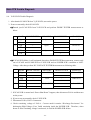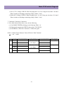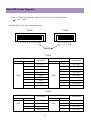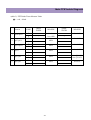
1
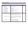
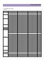
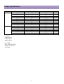
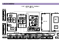
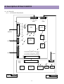
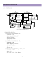
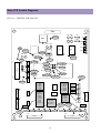
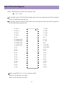
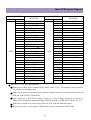
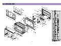
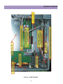
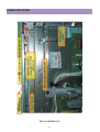
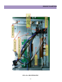
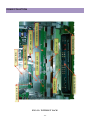
S/M No. : DSP115BEF0
Service Manual
42" PLASMA PDP MONITOR
CHASSIS : SP-115
✔ Caution
: In this Manual, some parts can be changed for improving, their
performance without notice in the parts list. So, if you need the
latest parts information,please refer to PPL(Parts Price List) in
Service Information Center (http://svc.dwe.co.kr).
DAEWOO ELECTRONICS Corp.
http : //svc.dwe.co.kr
Nov. 2002
Contents
1.Safety Precaution
2. Product Specification
2-1. SPECIFICATION
2-2. Available Input Signal
3. BLOCK DIAGRAM
4. Description Of Each BLOCK
4-1. A/V BLOCK
4-1-1. A/V BLOCK DIAGRAM
4-1-2. VIDEO PCB
4-1-3. JACK PCB
4-1-4. KEY PCB
4-1-5. LED PCB
4-2. DRIVING BLOCK
4-2-1. DRIVING BLOCK DIAGRAM
4-2-2. DRIVING WAVEFORM
5
6
6
8
10
11
11
11
12
16
17
17
18
18
4-2-3. DIGITAL PCB
4-2-4. X-SUS PCB
4-2-5. Y-SUS & SCAN PCB
4-2-6. CONNECTION PCB & DATA COF
4-3. POWER BLOCK
4-3-1. POWER BLOCK DIAGRAM
4-3-2. POWER PCB
5. SERVICE MODE
5-1. Entering SERVICE MODE
5-2. Default Values For SERVICE MODE Items
5-3. Description Of SERVICE MODE Items
6. Adjusting Method
6-1. Adjusting WHITE BALANCE
6-2. Adjusting DRIVING VOLTAGE And WAVEFORM
6-2-1. Adjusting POWER PCB
6-2-2. Adjusting X-SUS PCB
6-2-3. Adjusting Y-SUS PCB
FIG <6-1>. X-SUS PCB Adjusting Points
FIG <6-2>. Y-SUS PCB Adjusting Points
7. SOFTWARE UPGRADE Method
8. SET Disassemble/Assemble Method
8-1. Facts You Must Know When Disassembling/Assembling PDP SET
8-2. PCB Disassemble/Assemble Method
8-3. FRONT MASK Disassemble/Assemble Method
8-4. FILTER GLASS Disassemble/Assemble Method
-2-
19
21
25
27
29
30
30
31
33
33
33
34
37
37
38
38
39
39
41
42
43
46
46
46
47
47
9. Main PCB Trouble Diagnosis
9-1. VIDEO & JACK PCB Trouble Diagnosis
9-2. DIGITAL PCB Trouble Diagnosis
FIG<9-1>. DIGITAL PCB LAYOUT
9-3. X-SUS PCB Trouble Diagnosis
9-4. Y-SUS & SCAN PCB Trouble Diagnosis
9-5. CONNECTION PCB & DATA COF Trouble Diagnosis
9-6. POWER PCB Trouble Diagnosis
10. TROUBLE SHOOTING
10-1. Facts You Must Know When Diagnosing And Repairing
10-2. Representative Symptoms When Each PCB Breaks Down
10-3. Trouble Diagnosis And Repairing Method For Representative Symptoms
FIG<10-1> Trouble Diagnosis Flow when SHUT DOWN occurs
FIG<10-2> Trouble Diagnosis Flow when Low Voltage SHUT DOWN occurs
FIG<10-3> Trouble Diagnosis Flow when High Voltage SHUT DOWN occurs
FIG<10-4> Trouble Diagnosis Flow when Abnormal Discharge occurs
11. ASSEMBLY LIST
12. EXPLODED VIEW
13. FIGURE COLLECTION
FIG<1>. TOTAL
FIG <2>. Y-SUS & SCAN
FIG <3>. X-SUS
FIG <4>. VIDEO & JACK
FIG <5>. POWER
FIG <6>. INLET
FIG <7>. LEFT-UP
FIG <8>. LEFT-DOWN
FIG <9>. RIGHT-UP
FIG <10>. RIGHT-DOWN
FIG <11>. WITHOUT JACK
FIG <12>. DIGITAL
FIG <13>. AC SWITCH ASSEMBLY
FIG <14>. SCAN ASSEMBLY1
FIG <15>. SCAN ASSEMBLY2
FIG <16>. X-SUS ASSEMBLY
FIG <17>. FRONT MASK ASSEMBLY
FIG <18>. FRONT MASK INSIDE
FIG <19>. BACK COVER
FIG <20>. POWER ADJUSTING POINTS
FIG <21>. POWER HIGH VOLTAGE SWITCH
FIG <22>. HOW TO ADJUST VOLTAGE
-3-
49
49
55
61
62
65
71
72
73
73
73
77
80
81
82
83
84
85
86
86
87
88
89
90
91
92
93
94
95
96
97
98
99
100
101
102
103
104
105
106
107
FIG <23>. Y-SUS & SCAN PCB DIODE TEST
FIG <24>. SCANH PCB DIODE TEST
FIG <25>. SCANL PCB DIODE TEST
FIG <26>. 5 STEP GRAY SCALE PATTERN
14. Trouble Symptom Picture
Trouble Symptom Picture<1>.
Trouble Symptom Picture <2>.
Trouble Symptom Picture <3>.
Trouble Symptom Picture <4>.
Trouble Symptom Picture <5>.
Trouble Symptom Picture <6>.
Trouble Symptom Picture <7>.
Trouble Symptom Picture <8>.
Trouble Symptom Picture <9>.
Trouble Symptom Picture <10>.
Trouble Symptom Picture <11>.
Trouble Symptom Picture <12>.
108
109
110
111
112
112
113
114
115
116
117
118
119
120
121
122
123
-4-
1. Safety Precautions
(1) When moving or laying down a PDP Set, at least two people must be working. Avoid any impact
towards the PDP Set.
(2) Do not leave the broken PDP Set on for a long time. To prevent any further damages, after check the
broken Set s condition, make sure to turn the power (AC) off.
(3) When opening the BACK COVER, turn off the power (AC) to prevent electric shock. When a PDP is
on, high voltage and high current exist inside the Set.
(4) When loosening screws, check the connecting position and type of the screw. Sort out the screws and
store them separately. Because screws holding PCB are working as electric circuit GROUNDING,
make sure to check if any screw is missing when assembling.
(5) If you open the BACK COVER, you will see a Panel Gas Exhaust Tube (refer to FIG<10>). If this
part is damaged, entire PDP PANEL must be replaced. Therefore, when working, be careful not to
damage this part.
(6) A PDP Set contains different kind of connector cables. When connecting or disconnecting connector
cables, check the direction and position of the cable beforehand.
(7) When disconnecting connectors, unplug the connectors slowly with care. Especially when
connecting/disconnecting FFC (film) cables or FPC cables, do not unplug the connectors too much
instantaneously or strongly, and always handle the cables with care. (Refer to FIG<10>, FIG<11>)
(8) Connectors are designed so that if the number of pins or the direction does not match, connectors will
not fit. When having problem in plugging the connectors, make sure to check their kind, position,
and direction.
-5-
2. Product Specification
2-1. PRODUCT SPECIFICATION
ITEM
1. GENERAL
1-1. MODEL NO
1-2. CHASSIS NO
1-3. SCREEN SIZE
1-4. COUNTRY
1-5. RESOLUTION
1-6. REMOCON TYPE
1-7. SAFETY STANDARD
2. MECHANICAL
2-1. APPEARANCE
1) WITHOUT STAND
2) WITH STAND
3) CARTON BOX
2-2. WEIGHT
1) WITHOUT STAND
2) WITH STAND
3. ELECTRICAL
3-1. VIDEO INPUT
3-2. DTV/DVD INPUT
3-3. PC INPUT
3-4. SOUND INPUT
3-4. SPEAKER OUTPUT
3-5. POWER REQUIREMENT
3-6. POWER CONSUMPTION
3-8. RS-232 CONTROL
3-9. FUNCTION
1) SCALING
2) ZOOM
3) OSD
4) OTHERS
SPECIFICATION
DSP-4280GM(G, W, S)
SP-115
42 (16:9)
WORLD WIDE
853(H) X 480(V)
R-V28A (E)
UL, C-UL, CE, CB, FCC(CLASS B), CE(CLASS B), K-mark
WxHxD=1,039 x 628 x 80 mm
WxHxD=1,039 x 725 x 320 mm
WxHxD=1,256 x 800 x 327 mm
29.9 Kg
36.8 Kg
COMPOSITE(NTSC, PAL, SECAM, PAL-M/N, NTSC4.43)
& S-VHS(50/60Hz Y/C) 2 sets
1080 i, 720P, 480P , 480i
(Y, Pb/Cb, Pr/Cr COMPONENT SIGNAL) 2 sets
VGA ~ UXGA (15 PIN D-SUB) 1 sets
2 sets for VIDEO, 2 sets for DTV/DVD, 1 set for PC
8W(R) + 8W(L)
AC 100V~240V, 50/60Hz
320W
RS-232 Communication (for SOFTWARE UPGRADE)
PC: H/V SIZE and POSITION Adjusting
VIDEO/DTV/DVD : NOMAL, 16:9, PANORAMA, ENLARGE
LB, ENLARGE LBS
20 Scale ZOOMING & PANING
Support 11 Languages
STILL, SLEEP MODE, SOUND MODE
-6-
REMARK
Product Specification
ITEM
4. OPTICAL
4-1. SCREEN SIZE
4-2. ASPECT RATIO
4-3. NUMBER OF PIXELS
4-4. DISPLAY COLOR
4-5. PIXEL PITCH
4-6. PEAK LUMINANCE
4-7. CONTRAST RATIO
4-8. VIEWING ANGLE
5. USERCONTROL & ACCESSORIES
5-1 CONTROL BUTTON(SET)
SPECIFICATION
42 (106Cm) DIAGONAL
16:9
853(H)X480(V)
16.77 Million Colors ( 8BIT per each R,G,B)
1.08(H)X1.08(V)
300cd/ (WITH FILTER GLASS)
3000:1
Over 160 degree ( VERTICAL / HORIZONTAL)
AC POWER BUTTON(PUSH-PULL S/W)
MENU, SELECT, UP, DOWN, LEFT, RIGHT(SOFT S/W)
5-2. REMOTE CONTROL(R-V28)
POWER, INPUT SELECT, DISPLAY, ZOOM-,ZOOM+,
MENU, UP, DOWN, VOLUME, FREEZE, SCREEN MODE,
SOUND MODE, SLEEP
5-3. ACCESSORIES
REMOCON CONTROLLER, BATTERY,
INSTRUCTION MANUAL, A/V CABLE,
STAND, WALL HANGER, SPEAKER R/L
-7-
REMARK
Product Specification
2-2. Available Input Signal
(1) PC
Resolution
640x350
640x400
640x480
720x400
720X480
720X576
800x600
832x624
1024x768
1152X864
1152x900
1280X720
1280X960
H Freq. (KHz)
31.469
37.861
24.823
30.48
31.469
37.861
31.469
35
37.861
37.5
39.375
43.269
31.47
31.469
37.927
31.54
15.63
35.156
35.16
37.879
48.077
46.875
53.674
49.726
48.193(48.077)
48.363
53.95
56.476
60.241
60.023
68.677
80.66
70.84
54
63.851
67.5
77.094
61.796
71.713
45
60
75
85.938
V Freq. (Hz)
70.1
85.1
56.4
60.0
70.1
85.1
59.9
66.7
72.8
75.0
75.0
85.0
60.0
70.1
85.1
60.0
25.0
56.3
57.2
60.3
72.2
75.0
85.1
74.0
59.3(59.8)
60.0
66.1
70.1
74.9(74.6)
75.0
85.0
100.0
84.0
60.0
70.0
75.0
85.0
66.0
76.0
60.0
60.0
75.0
85.0
-8-
Remark
IBM
VESA
NEC
PGA
IBM (DOS)
VESA
DOS
Macintosh
VESA
VESA
IBM
VESA
VGA
IBM
VESA
480P
PAL
VESA
VESA
VESA
VESA
VESA
VESA
Macintosh
Macintosh(OAK)
VESA
XGA
HP&VESA
Macintosh
VESA
VESA
Fujitsu
SUN
VAX
VESA
VESA
VESA
SUN
SUN
720P
VESA
VESA
VESA
Patt No.
203
11
15
871
204
16
17
18
19
20
21
22
876
13
14
953
950
23
24
24
25
26
27
28
29
30
890
31
32
33
34
939
926
936
35
36
37
38
39
954
40
41
42
Product Specification
Resolution
1280X1024
1600X1200
H Freq. (KHz)
46.433
63.981
70.66
74.88
78.125
78.855
79.976
81.13
91.146
62.5
75
81.25
87.5
93.75
100
V Freq. (Hz)
43.4
60.0
66.5
70.0
72.0
74.1
75.0
76.1
85.0
48.0
60.0
65.0
70.0
75.0
80.0
(2) DTV
-1080i/ 60 Hz
-720P / 60 Hz
-480P / 60 Hz
(3) VIDEO
-PAL, PAL-M, PAL-N
-NTSC , NTSC4.43
- SECAM
-9-
Remark
VESA
VESA
VAX
NEC
HP & HITA
Sony & NEC
VESA
SUN
VESA
VESA
VESA
VESA
VESA
VESA
VESA
Patt No.
205
44
937
921
206
46
47
927
48
50
862
863
864
865
-10-
4. Description Of Each BLOCK
4-1. A/V BLOCK
4-1-1. A/V BLOCK DIAGRAM
IR
GND
GND
S5V
2
4
COLUM1
1
5
COLUM2
P_LED
1
COLUM3
3
2
DATA2
DATA1
GND
3
5
4
6
P601
P602
P603
2
1
to
DIGITAL
40
39
GND STB5V
NC
G0
NC
G1
NC
G2
DVS
G3
DHS
G4
V_MUTE
G5
S_RESET
G6
NC
G7
DEN
GND
GND
B0
R0
B1
B2
R1
R2
B3
B4
R3
R4
B5
R5
B6
B7
R6
R7
GND
DCLK GND
DEN
VVS
S_RESET
V_MUTE
DVS
IC600
PW171
DHS
VCLK
IC406
DPTV-MVS
VHS
VPEN1
VPEN
GBLKSLP GPEN
GSOG
DECOE
GHSFOUT
GCOAST
GREF
DCLKB
IC401
SAA7118
PA5
5
STB5V
4
GND
GCLK
3
to PWR
2
1
GHS
IC500
CXA3516
CCOMB
PWR_CLT
YCOMB
LED_P
GVS
PA4
8
to PWR
LED_P
GND
7
GND
6
P5V
5
GND
4
GND
3
P12V
2
P12V
1
VIN
P12V
VPC
P12V
HPC
GND
GND
GND
BPC
GND
SEL1
SEL2
GPC
GND
SEL3
GND
RPC
GND
SCL
G/Y_DTV
SDA
GND
GND
B/PB
GND
GND
TXD1
R/PR
RXD1
GND
GND
Y_DVD
DSCL
DSDA
GND
GND
CB
NC
GND
NC
CR
ID_JACK GND
GND
CO
S_MUTE GND
MSP_RST YO
GND
GND
9
IC400
u64083
STB5V
P502
10
NUL
JACK
PCB
1
25
26
50
26
50
1
25
KEY
PCB
1
2
3
4
2
1
3
4
PA6
PA502
R_OUT
IC706
CXA2151
to PWR
IC704
CXA2069
L_OUT
IC700
MSP3420
RIGHT
LEFT
IC702
TDA7480
IC701
TDA7480
5
1
PA601
LED
-11-
2
3
4
5
PA602
6
Description Of Each BLOCK
4-1-2.VIDEO PCB
- PROCESS Various Signal (PC, COMPONENT, COMPOSITE ) to produce 24BIT DIGITAL
output
1) IC and TP
(1) IC400(UPD64083)
-Using 3D COMBFILTER to separate COMPOSITE signal to Brightness
Signal(Y) and Color Signal(C)
*TP ( Input : COLOR BAR PATTERN )
A. YCOMP : Brightness Signal(Y)
B. CCOMP : Color Signal (C)
(2) IC401 (SAA7118E)
-Receive NTSC, SECAM, PAL VIDEO by COMPOSITE(V) , S-VHS(Y.C)
COMPONENT (Y Cb Cr) and process signal
*TP
A. DECOE : CHIP ENABLE part. When signal process is done by IC401,
output 3.3V DC LEVEL
-12-
Description Of Each BLOCK
(3) IC406(DPTV-MVS)
-A Scan Rate Converter which converts Interlace signal into Progressive signal
*TP
A. VVS : VERTICAL SYNC (output by DPTV-MVS)
B. VHS : HORIZONTAL SYNC (output by DPTV-MVS)
C. VCLK : CLOCK (output by DPTV-MVS)
-13-
Description Of Each BLOCK
(4) IC500(CXA3516R)
-3-channel 8-bit 165MSPS A/D converter which process PC , DTV signal
* TP
A. GCOAST : COAST CONTOL Signal for PLL (input by CXA3516)
B .GHS : HORIZONTAL SYNC for GRAPHIC (output by CXA3516)
C. GCLK : CLOCK for GRAPHIC (output by CXA3516)
-14-
Description Of Each BLOCK
D. GFBK : SYNC for PLL
(5) IC600(PW171)
- Image processor IC
*TP
A. DEN : DATA ENABLE (output by PW171)
B. DHS : HORIZONTAL SYNC (output by PW171)
-15-
Description Of Each BLOCK
C.DVS : VERTICAL SYNC for DISPLAY (output by PW171)
D. DCLKB : CLOCK for DISPLAY (output by PW171)
4-1-3. JACK PCB
- Separate and process various VIDEO and AUDIO signal
(1) IC706(VIDEO /SYNC SELECTOR)
- This chooses Y Cb/Pb Cr/Pr or RGB signal to output Y Cb/Pb Cr/Pr, to separate SYNC, and to
perform SYNC COUNTER.
(2) IC704(7_INPUT 3_OUTPUT AUDIO/VIDEO SWITCH)
- The IC perform AUDIO or VIDEO SWITCHING
(3) IC700(MULTI STANDARD SOUND PROCDSSOR)
-AUDIO SINGNAL VOLUME control, EQUALIZER control
-16-
Description Of Each BLOCK
*TP
R_OUT(L_OUT) : AUDIO SIGNAL that goes into MSP3420 before AUDIO PROCESSING
(4) IC701 .IC700 (TDA 7480)
*TP
A. RIGHT(LEFT) :AMP input signal before 30dB amplification
4-1-4.KEY PCB
- Input PCB using KEY
4-1-5.LED PCB
- PCB for REMOCON CONTROL
-17-
Description Of Each BLOCK
4-2 DRIVING BLOCK
4-2-1. Driving BLOCK DIAGRAM
SCAN
TOP
DATA
INPUT
CONTROL
SIGNAL
Y-SUSTAIN
ENERGY
RECOVERY
SCAN
ERASE
WRITING
TIMING
CNOTROL
&
DATA
INTERFACE
Verase
X-SUSTAIN
ENERGY
RECOVERY
SHELF
PANEL
SCAN
BOTTOM
DATA
DRIVER
Vsus
Vadd
Vdr
Vsus
POWER
Vadd
Vstb/Video/etc.
Driving circuit block looks like above diagram. First, within the Digital-board, timing control / data
interface signals input to Y / X / DATA-board. Also, low voltage and high voltage powers such as
15V / 5V / Vsus / Yer / Vadd are supplied. SCAN is divided into two PCB(upper and lower) and
DATA driver can drive 7 COF module. Also Connection-board which is located at the lower part of
the panel, is divided into two PCB. It transfer 5V / Vadd power supply as well as various Y / X /
DATA-board. Vadd power supply is transferred from Power module to X-board through Connectionboard to Data driver.
-18-
Description Of Each BLOCK
4-2-2. Driving Waveform
Y-DRIVING
1 SUB-FIELD
230V
173V
BV
173V
166V
GND
Yn
-62V
ERASING
SCAN
X-DRIVING
173V
163
158V
155V
GND
H
Z-DRIVING
68V
GND
SUSTAINING
X-SHELF
FULL WRITING
ADDRESSING
Zn
L
PDP Driving signal is largely divided into three(Y, X, Z) as shown above. They are outputs of Yboard, X-board, DATA-board (COF) respectively. Each Sub-field is divided into ADDRESSING,
SUSTAINING, ERASING parts. FULL WRITE pulse from Y-board adds once per frame(~
= 16ms).
1) FULL WRITING
It is a process that in order to display new image, every cell s condition must be uniformed to erase
wall charge made by previous discharge and make new wall charge for next address discharge.
Ramp shape signal is added to supply every cell uniform wall charge.
To decrease Background luminescence and improve contrast, it is applied once per frame.
Full Writing signal output by Y-board is Vsus electric potential supplied by power module plus
ramp-shape output signal made by DC-DC Converter(TY1).
2) ADDRESSING
Previous to SUSTAINING, it is procedure to select charging cell for image display.
In other words, it is the stage to make wanted cell to form wall charge.
During this stage, SCAN block operate in Y-board and SHELF block (X_HIGH) in X-board.
-19-
Description Of Each BLOCK
3) SUSTAINING
After the Addressing period, this stage is to add Sustaining pulse to selected cell to make the
SUSTAINING discharge continue.
For each X, Y-board sustain block, opposite-polarity rectangular pulse which have ER_H SUS_H
ER_L SUS_L order, is distributed to Panel s X,Y electrode at a constant frequency.
4) ERASING
Removing operation for Electrical discharge inside each cell to address new data in next Sub-field.
It is a Ramp output signal similar to Full Writing signal.
Ramp-down block operates in Y-board and Shelf block (X_N_SHELF) operates in X-board.
-20-
Description Of Each BLOCK
4-2-3.
DIGITAL PCB
ID1
1st_chip(A500K180)
ID2
2nd_chip(A500K270)
ID3 & ID4
RGB DATA [0:3]
Inverse Gamma
&
Dithering
Weight
Conversion
SDRAM
(64M x 2)
PISO
SDRAM
Controller
APL
Detection
PDP Driving
Timing Controller
Z Driver Control Signal
Y Driver Control Signal
ID33
X Driver Control Signal
ROM
(M27C1024)
: Data Flow
: Control Address Flow
: ROM Data Flow
<DSP-4280GM Digital B/D Block Diagram>
1. Digital PCB s Main Part
(1)Actel FPGA A500K180-PQ208 : 1 EA
- Location No. : ID1
- Power : Internal 2.5V, I/O 3.3V
- Package : PQFP 208
- Typical Gates : 150,000
- User I/O : 164
(2)Actel FPGA A500K270-BG456 : 1 EA
- Location No. : ID2
- Power : Internal 2.5V, I/O 3.3V
- Package : BGA 456
- Typical Gates : 215,000
- User I/O : 362
(3)SDRAM( K4S643232E-TC70 86pin TSOP ) : 2 EA
- Location No. : ID3~4
- Power : 3.3V
- Size : 64 M ( 512K * 32 bit * 4 Banks )
-21-
Z Driver Data Signal
Data Interface
ROM
Controller
Description Of Each BLOCK
(4)50MHz Clock Oscillator : 1 EA
- Location No. : XD1
- Power : 3.3V
(5)Buffer IC( 74LCX541 ) : 17 EA
- Location No. : ID9~25
- Power : 5V
- Input Voltage : 3.3V
- Output Voltage : 5V
(6)Buffer IC( 74LCX541 ) : 4 EA
- Location No. : ID5~8
- Power : 3.3V
- Input/Output Voltage : 3.3V
(7)EPROM( M27C1024-PLCC44 ) : 1 EA
- Location No. : ID33
- Power : 5V
- Input Voltage : 3.3V
- Output Voltage : 5V
(8)2.5V Regulator( LP3964EMP-2.5 )
- Location No. : ID32
- Input Voltage : 5V
- Output Voltage : 2.5V
(9)EMI Reduction IC ( P2040 )
- Location No. : ID34
- Power : 3.3V
2. Data Flow
(1)Input from Video PCB
- 8bit Data per each R,G,B ( synchronized by DCLK)
- DVS, DHS, DEN, S_RESET, V_MUTE, DCLK(33.5 MHz)
(2)Inverse Gamma & Dithering Block
- After mapping input data according to Reverse Gamma Correction Table , execute
Dithering Process .
(3)Weight Conversion Block
- Map input data according to Weight Conversion Table , which is based on optimum PDP
Driving Weight Pattern.
-22-
Description Of Each BLOCK
(4)ROM & ROM Controller Block
- ROM contains Reverse Gamma Correction Table , Weight Conversion Table , APL
Table and so on. Rom Controller Block generate Address & Control signal for receiving
these data from ROM
(5)PISO(Parallel Input Serial Output) Block
- Load 10 pixels per each R,G,B data with parallel type and shift them with serial type in order
of Weight ( LSB first ). These shifted data is stored in Internal Memory of A500K270(ID2)
with based on DCLK(33.5MHz). After that, those data go into External Frame Memory
(SDRAM) in order of Weight with based on CLK50M. In other words, PISO Block execute
three steps Data Load
Data Shift & Internal Memory Write
Internal Memory Read &
External SDRAM Write successively. To process with real time, there are three PISO
Blocks.
(6)SDRAM & SDRAM Control Block
- Generate Address/Control signals for SDRAM. There are 2 SDRAMs (64M 32-bit SDRAM),
which store 1 Frame s R,G,B data in order of Weight respectively to process with real time.
(7)Data Interface Block
- R,G,B data ouput from SDRAM is stored by line in Data Interface Block. These data is output
in order matched by Data Driver IC(Z Driver IC) s input sequence. Our PDP has 853 Data
Lines per each R,G,B, and need 853*3=2559 bit s storage. To process with real time,
actually need 2559*2=5118 bit s storage.
3. PDP Driving Timing Control
(1)X-SUS Driving Control Signal Block
- Generate Control Signals to drive X-SUS PCB. There are 6 Control Signals as follows.
- X_SUSH, X_SUSL, X_ERH, X_ERL, X_HIGH, X_NSHELF
(2)Y-SUS Drving Control Signal Block
- Generate Control Signals to drive Y-SUS PCB & Scan Drvier IC. There are 12 Control Signals
as follows.
- Y_SUSH, Y_SUSL, Y_ERH, Y_ERL, Y_SC20_2, Y_SC20_3, Y_SC21_7, Y_SC21_9,
Y_BLK, Y_CLK, Y_SI1, Y_SI2
(3)Z Driving Control Signal Block
- Generate Control Signals to drive DATA COF (Z Driver IC). There are 8 Control Signals as
follows.
- Z1_CLK1, Z1_CLK2, Z2_CLK1, Z2_CLK2, Z1_BLK, Z1_STB, Z2_BLK, Z2_STB
-23-
Description Of Each BLOCK
(4)Sub Control Signal Block
- Generate some Control Signals to control Data Interface Block and SDRAM Control
Block . There are 5 Control Signals as follows.
- F_SUBF, CLK_480, OUT_CLK, F_32SFT, SLCT
(5)APL Detection Block
- Detect the amount of input Data, which is so-called APL (Average Picture Level), and give
APL to Timing Controller Block in order to control Power Consumption of PDP Set.
-24-
Description Of Each BLOCK
4-2-4.
X-SUS PCB
1) X_SUSTAIN PCB block diagram
P201A
15V
GND Vadd GND GND GND GND
P202A
NC
11
Vsus Vsus
NC
1
X
X
X
X
X
X_N_
Vadd GND GND _HIGH SHELF GND GND _ERL _ERH _SUSL _SUSH 5V
12
1
X_sustain
X_shelf
PU1
PU2
PU3
PU4
PU5
PU6
X_ELECTRODES
2) Structure of X_SUSTAIN PCB
X_SUSTAIN BLOCK SUS_H / SUS_L / ER_H / ER_L(Energy Recovery Circuit)
HIC Structured
Vshelf Generating Circuit
From Vsus(173V) to X_HIGHT(163V) voltage generating circuit
15V to X_ N_SHELF(5V) voltage generating circuit
Control Voltage by Variable Resistor
RU1
LOGIC Circuit that processes various waveform timing signal
-25-
Description Of Each BLOCK
3) Power Supply
Vsus - Supplied by POWER MODULE. Supplies X-SUS as well as generates X-HIGHT
voltage.(173V)
15V - Supplied by POWER MODULE. Supplies FET driving power as well as generates
X_N_SHELF voltage(5V).
5V - Supplied through CONNECTION-board from DIGITAL-board. Used for LOGIC IC Power.
4) Signal
X_SUSTAIN
SUS_H / SUS_L / ER_H / ER_L (Supplied from P202A)
X_SHELF
X_N_SHELF / X_HIGHT (Supplied from P202A)
5) SUSTAIN BLOCK
LESONANCE COIL
LESONANCE FREQUENCY
-26-
Description Of Each BLOCK
4-2-5.
Y-SUS & SCAN PCB
1) Y_SUSTAIN PCB block diagram
P101A
15V
GND GND
P103A
Y_
V
V
NC ERASE _SUS _SUS
1
7
P102A
5V
GND GND
11
GND GND
Y_
ERL
Y_
Y_
Y_
ERH SUSL SUSH GND
1
Y_erase
Y_scan
Remp
_up
&s/w
Scan
(PY1)
Scan
(PY1,4)
Scan
(PY1,4)
IY8/IY27
_Vcc
Remp
_down
&s/w
shelf
Scan
(PY4)
15V_Y2
15V_Y2
Y
_ramp_
down
DC-DC
Y_ramp
_up
Y
_ramp
_up
Y_sustain
5V_Y2
Ramp_up
S/W
Ramp_down
S/W
15V_Y2
Y_erase
5V_Y2
DC-DC
Y_shelf
Y_shelf
15V_Y3
15V_Y2
DC-DC
Y_scan
5V_Y2
Y_scan
5V_Y3
PY1
5V_Y3
PY2
PY3
SCAN-BOARD
Y_ELECTRODES
-27-
PY4
Description Of Each BLOCK
2) Y_SUSTAIN PCB Structure
SUSTAIN BLOCK
SUS_H / SUS_L / ER_H / ER_L (Energy Recovery Circuit)
Structured with HIC
RAMP_UP , RAMP_DOWN waveform generating circuit
RAMP_UP_S/W , RAMP_DOWN_S/W
Y_SCAN
-62V(based on GND) Applying Circuit
Y_SHELF
70V(based on GND) Applying Circuit
Yer 166V Applying Circuit
RAMP_UP / Y_SCAN_VH / DC-DC converter circuit that generating Y_SCAN_GND s
voltage
LOGIC Circuit that processes various waveform timing signal
3) Power Supply
Vsus - Supplied from POWER MODULE.(173V)
15V - Supplied from POWER MODULE and used for FET s driving power and input powers of 3
DC-DC converter. Also, generates output voltage of each Y-RAMP_UP / Y-SCAN /
Y_SHELF(Y_SCAN_GND).
5V - Supplied from POWER MODULE through DIGITAL-board. Used for LOGIC IC power
supply. Also, power supply of 5V_Y2, 5V_Y3 is supplied through 7805 regulator from DCDC converter Trans TY2 s output.
Yer - Supplied by POWER MODULE. (166V)
GND - Power supply GND / Y1 / Y2 / Y3
4) Signal
Y_SUSTAIN
SUS_H / SUS_L / ER_H / ER_L(supplied by P102A)
Y_ERASE (supplied by P103A)
Y_SCAN (supplied by P103A)
Y_RAMP_DOWN & S/W (supplied by P103A)
Y_RAMP_UP & S/W (supplied by P103A)
SCAN CLK / SI1 / SI2 / BLK (supplied by P103A)
-28-
Description Of Each BLOCK
4-2-6. CONNECTION PCB & DATA COF
1) Structure of CONNECTION PCB
Divided into 2 PCBs (CONN-LEFT & CONN-RIGHT)
CONN-LEFT
From DIGITAL PCB through connector P304, data signal and 5V IC Power
are supplied. Vadd Power is supplied to PC 5~7 through PC08A.
CONN-RIGHT
From DIGITAL PCB through connector P304A, data signal and 5V IC
Power are supplied. 5V Power is supplied to X-board through P202. Also, Data signals are
supplied from DIGITAL PCB through P302A and X-sustain/X-shelf signals are supplied from
X-SUS PCB through P202. Vadd Power is supplied to PC 1~4 from X-SUS PCB through P202
and to CONN-LEFT through PC8A1 and PC08A.
2) Structure of DATA COF
7 COF Type module(PC 1~7)
DATA signals are transferred to CONNECTION PCB from DIGITAL PCB through P304A /
P303A / P302A. And through PC 1~7 each are transferred to DATA COF.
5V supplied from DIGITAL PCB through connector P304A / P303A. Vadd flows POWER PCB
X-SUS PCB
connector P202 CONNECTION PCB DATA COF.
-29-
Description Of Each BLOCK
4-3. POWER BLOCK
4-3-1. POWER BLOCK DIAGRAM
Main B+
AC Input
Line
PFC
5V out
Vlow
Filter
12V out
B+
15V
30V out
15V out
Sequence
ST- BY
Control
5V out
Block
5V
3.3V out
IC B+
Main B+
IC ON/OFF
Vadd
Vadd
Block
Discharge
IC ON/OFF
Main B+
Vsus
Vsus
IC B+
POWER
Vyer
ON/OFF
Control
Protectio n
Block
Vyer
ST- BY
If Power is ON , V_PFC and V_LOW BLOCK is working and Voltage generated in V_LOW s
2nd Coil actuates V_ADD. After V_ADD is ON , 2nd Voltage generated in V_ADD BLOCK
acutates V_SUS BLOCK again.
-30-
Description Of Each BLOCK
4-3-2. POWER PCB
Rating : AC100~240 V, Single-Phase
Regulation Method : Transistor & Switching Method
Rating Input Frequency : 50~60Hz, Inrush Current : under 35A.
Output Voltage is as follows.
1
2
3
4
5
6
7
Vsus
Vadd
Vyer
Vdr1
V1
V2
V3
8
9
10
V4
V5
Vstb
Rating Variable
Range
(V)
(V)
175
10
70
10
160
10
15.5
5
12
17
-17
5.1
3.6
5
Tolerance
(V)
0.75
0.25
0.6
0.75
0.75
0.55
0.33
0.5
Voltage(Vdc)
Allowable
overshoot
Voltage(V)
200
90
180
18
6
13.6
18
-18
6.5
3.66
6
Ripple
Voltage
(mVp-p)
2000
500
500
50
50
50
50
50
50
33
50
OVP
(V)
200
100
18
Ripple Noise
Voltage
(mVp-p)
500
300
500
100
100
100
100
100
100
66
100
Rating
(A)
1.5
1
0.1
1
1
0.6
0.7
0.7
1
1
0.5
Current(Adc)
When
OCP
Lode
(A)
change
0.1~1.5 Over 3.2
0.1~1 Over 2.0
0~0.15
0.1~1
1.4
0.1~1
0~1
0~1
0.1~1
0.1~1
0~1
0~1
* When Protect Circuit operates, all Outputs except Vstb are suspended. But, when
Vstb is abnormal, all Outputs are suspended.
* OVP(Over Voltage Protection), OCP(Over Current Protection)
The above table s Output Voltage output from the following connector.
(based on the Parts Side s silk name of POWER PCB)
Vsus
Vsus
Vyer
NC
HG
HG
Vdr1
NC
Vsus
Vsus
P2
HG
HG
HG
HG
P1
NC
LG
NC
LG
VG
Vstd
V2
VG
VG
V2
V4
NC
NC
P4
NC
P5
VG
NC
LG
VG
PR
LG
V5
V1
NC
V1
V3
P3
SG
SG
V3
NC
-31-
P6
Vadd
HG
Vdr1
Description Of Each BLOCK
* P2 is connected to Y-SUS PCB s P101A
P1 is connected to X-SUS PCB s P201A
P4 is connected to VIDEO PCB s PA4
P5 is connected to VIDEO PCB s PA5
P3 is connected to DIGITAL PCB s P301A
P6 is connected to JACK PCB s PA6.
-32-
5. SERVICE MODE
5-1. Entering SERVICE MODE
Push Remote controller’s “UP”
MUTE
DISPLAY
SERVICE adjust MODE.
5-2. Default Values fot SERVICE MODE
1) PW171
-SUB-BRIGHTNESS : 28
-SUB-CONTRAST : 40
-R-BIAS : 68
-G-BIAS : 65
-B-BIAS : 70
-R-GAIN : 67
-G-GAIN : 45
-B-GAIN : 78
2) SAA7118
-SUB BRT : 128
-SUB CONT : 50
-SUB CLR : 64
-SUB TNT : 0
-SUB SRP : 10
3) DPTV
-SUB BRT : 59
-SUB CONT : 13
4) CXA3516
-SUB CONT : 58
-Cb OFFSET : 39
-Cr OFFSET : 37
-HYS
:3
-THRSLD : 14
-33-
MUTE
BUTTON to enter
SERVICE MODE
5) MSP34X0
-PRESCALE : 22
5-3. Description of SERVICE MODE Items
1) PW171
(Note) This article is for adjustment after replacement of VIDEO PCB. These Values may vary
from set to set. Therefore if these values are recorded before replacing VIDEO PCB, you do
not need to adjust WHITE BALANCE additionally. The set up can be done using the
recorded values.
(1)SUB BRT : Set up BRIGHT standard value of PW171.
(2) SUB CONT : Set up CONTRST standard value of PW171.
(3) BIAS R : Set up RED BIAS value during WHITE BALANCE
(4) BIAS G : Set up GREEN BIAS value during WHITE BALANCE
(5) BIAS B : Set up BLUE BIAS value during WHITE BALANCE
(6) GAIN R :Set up RED GAIN value during WHITE BALANCE
(7) GAIN G : Set up GREEN GAIN value during WHITE BALANCE
(8) GAIN B : Set up BLUE GAIN value during WHITE BALANCE
2) SAA7118
(Note) This article is not for adjustment after replacement of VIDEO PCB. Therefore do not change
initial values.
(1) SUB BRT : Set up BRIGHT standard value of SAA7118.
(2) SUB CONT : Set up CONTRAST standard value of SAA7118.
(3) SUB CLR : Set up COLOR standard value of SAA7118.
(4) SUB TNT : Set up TINT standard value of SAA7118.
(5) SUB SRP : Set up SHARPNESS standard value of SAA7118.
3) DPTV
(Note) This article is not for adjustment after replacement of VIDEO PCB. Therefore do not
change initial values.
(1) SUB BRT : Set up BRIGHT standard value of DPTV MVS.
(2) SUB CONT : Set up CONTRAST standard value of DPTV MVS.
-34-
SERVICE MODE
4) CXA3516
(Note) This article is not for adjustment after replacement of VIDEO PCB. Therefore do not
change initial values.
(1) SUB CONT : Set up CONTRAST standard value of CXA 3516
(2) Cb OFFSET : Set up BLACK LEVEL of Cb CHANNEL
(3) Cr OFFSET : Set up BLACK LEVEL of Cr CHANNEL
(4) HYS : Set up HYSTERISIS of SYNC
(5) THR SLP : Set up THRESHOLE of PEDESTAL LEVEL
5) MSP34X0
(Note) This article is not for adjustment after replacement of VIDEO PCB. Therefore do not
change initial values.
(1) PRESCLE : Set up AUDIO output signal’ s magnitude
6) MISC
(1) TST PTRN AT : Changing TEST PATTERN (RED
GREEN
BLUE
BLACK
WHITE )
every minute automatically.
(2) TST PTRN MA : Changing RED
GREEN
BLUE
BLACK
WHITE TEST PATTERN
manually using VOLUME UP KEY.
(3) AT PWR : ON - Condition where turning AC power on, automatically turns the SET on.
OFF -Condition where turning AC power on makes the Set STAND BY, and
Remocon’ s POWER on turns the set on from STAND BY state.
(4) JACK : Set up depending on JACK BOARD’ s input MODE
- MULTI : Used by DSP-4280 series
- MONITOR : Used by DSP-4282 series
- MONITOR+ : Used by DSP-4282 series with DSP-JU20 attached.
(Note) Wront setup causes displaying problem. So you must be careful when SETTING.
(5) PXL SFT
ON - Moving screen up, down left and right by some PIXELs every 20 seconds.
OFF - Fixing PIXEL position. No movement on screen.
(Note) PIXEL SHIFT function is solution to PDP’s characteristic phenomenon, so-called “Image
Sticking” problem. Leave this function ON, When displaying many fixed screen like PC
screen. When this function is ON the screen will move a little for every fixed interval but a
human eye can not recognize it well.
7) INFOR
-35-
SERVICE MODE
(1) VER : Displaying Software’s VERSION
8) RESET
(1) EDID
(2) LEVEL 1 : RESET SERVICE MODE Condition’s All Values.
(3) LEVEL 2 : RESET SERVICE MODE Condition’s All Values except PW171 values
(4) FACTORY : RESET to factory shipping initialiaztion.
-36-
6.Adjusting Method
6-1. Adjusting WHITE BALANCE
(1) Input 5 STEP GRAY SCALE PATTERN to Video Input Terminal. (refer to FIG<26>)
(2) Set the SCREEN MODE to NORMAL .
(3) Enter SERVICE MODE by inputting remote controller s
=> MUTE
UP
MUTE
DISPLAY
BUTTON, and then select PW171 and check Default Values of SERVICE MODE
Items. (refer to article 5. Service Mode)
(4) Attach WHITE BALANCE METER(FACTORY USE METER: CA-100) SENSOR to 80% Gray
Scale part. (refer to FIG<26>)
(5) Adjust WHITE BALANCE by varying R,G,B GAIN
-. Control R,G,B GAIN values so that the ranges are within Default Value
10.
If deviate from the range, classify the SET disqualified.
-. Set color coordinate to x = 0.280
0.01, y = 0.290
0.01 and color temperature
to above or equal to 10,000 K.
(6) Attach WHITE BALANCE METER s SENSOR to 40% Gray Scale part. (refer to FIG<26>)
(7) Adjust WHITE BALANCE by varying R,G,B BIAS
-. Control R,G,B BIAS values so that the ranges are within Default Value
5.
If deviate from the range, classify the SET disqualified.
-. Set color coordinate to x = 0.280
0.01, y = 0.290
0.01.
(8) Repeat above (4) ~ (7) until color coordinate is x=0.280, y=0.290. Attach WHITE BALANCE
METER s SENSOR to 100% Gray Scale part. (refer to FIG<26>) Control SUB CONTRAST so
that LUMINANCE is above or equal to 140 Cd/m2.
(9) Enter MENU BUTTON and Exit SERVICE MODE.
-37-
Adjusting Method
6-2. Adjusting Driving Voltage and Waveform
6-2-1. Adjusting POWER PCB
(Note.1) Factory adjusted optimum voltage is stated at the LABEL located above the VIDEO PCB.
(refer to FIG<1>)
(Note.2) After replacing POWER PCB, adjust each voltage to optimum control voltage stated at
the LABEL.
(Note.3) Screen Condition : Enter SERVICE MODE and run TEST PATTERN FULL WHITE
(refer to 5. Service Mode)
(Note.4) Contact MULTIMETER s (-) TIP on the CHASSIS GROUND and (+) TIP on the
adjusting TP. (refer to FIG<22>)
(Note.5) Because adjusting while the SET is in operation, be cautious not to touch other parts
than adjusting TP with MULTIMETER s TIP. Make sure to use Plastic adjusting tool to
adjust VOLUME. (refer to FIG<22>)
1) Vsus(SUSTAIN Voltage) : Discharge Sustain Voltage
METER used : DIGITAL MULTIMETER (DC Voltage Measure Mode)
Adjusting TP : TP1 (refer to FIG<20>)
Adjusting VOLUME : RV500 (refer to FIG<20>)
Standard Voltage : 173V (This value could be different from the optimum
adjusting voltage)
Optimum adjusting Voltage : Stated in the LABEL (refer to FIG<1>)
2) Vyer(ERASE voltage) : Erase operation initial voltage of Last Sustain Pulse
METER used : DIGITAL MULTIMETER (DC Voltage Measure Mode)
Adjusting TP : TP3 (refer to FIG<20>)
Adjusting VOLUME : RV501 (refer to FIG<20>)
Standard Voltage : 166V (This value could be different from the optimum
adjusting voltage)
Optimum adjusting Voltage : Stated in the LABEL (refer to FIG<1>)
3) VADD(ADDRESS voltage) : DATA Input Voltage
METER used : DIGITAL MULTIMETER (DC Voltage Measure Mode)
Adjusting TP : TP2 (refer to FIG <20>)
Adjusting VOLUME : RV300 (refer to FIG <20>)
Standard Voltage : 72V (This value could be different from the optimum
adjusting voltage)
Optimum adjusting Voltage : Stated in the LABEL (refer to FIG<1>)
6-2-2. Adjusting X-SUS PCB
-38-
Adjusting Method
(Note.1) Factory adjusted optimum voltage is stated in the LABEL above the VIDEO PCB.
(refer to FIG<1>)
(Note.2) After replacing X-SUS PCB, adjust each voltage to the optimum adjusting voltage as
stated in the LABEL
(Note.3) Screen Condition : After entering SERVICE MODE, run TEST PATTERN FULL
WHITE (refer to 5. Service Mode)
(Note.4) Contact MULTIMETER s (-) TIP on the CHASSIS GROUND and (+) TIP on the
adjusting TP. (refer to FIG<22>)
(Note.5) Because adjusting while the SET is in operation, be cautious not to touch other parts
than adjusting TP with MULTIMETER s TIP. Make sure to use Plastic adjusting tool to
adjust VOLUME. (refer to FIG<22>)
1) Vx_shelf (x_shelf Voltage) : X electrode sustaining voltage when writing
DATA
METER used : DIGITAL MULTIMETER (DC Voltage Measure Mode)
Adjusting TP : DCU16 (+) electrode (refer to FIG<6-1>, FIG<3>, and the
following Figure )
Adjusting VOLUME : RU1 (refer to FIG<6-1>, and FIG<3>)
Standard Voltage : 158V (This value could be different from the optimum
adjusting voltage)
Optimum adjusting Voltage : Stated in the LABEL (refer to FIG <1>)
(-)
(+)
DCU16
6-2-3. Adjusting Y-SUS PCB
(Note.1) Factory adjusted optimum voltage is stated in the LABEL located above the VIDEO
PCB. (refer to FIG<1>)
(Note.2) After replacing Y-SUS PCB, adjust each voltage to the optimum adjust voltage as stated
in the LABEL
(Note.3) Screen Condition : After entering SERVICE MODE, run TEST PATTERN FULL
WHITE (refer to 5. Service Mode)
(Note.4) Contact MULTIMETER s (-) TIP on the CHASSIS GROUND and (+) TIP on the
adjusting TP. (refer to FIG<22>)
(Note.5) Because adjusting while the SET is in operation, be cautious not to touch other parts
than adjusting TP with MULTIMETER s TIP. Make sure to use Plastic adjusting tool to
adjust VOLUME. (refer to FIG<22>)
-39-
Adjusting Method
1) Ramp Up Slope Adjustment
Adjusting VOLUME : RY2 (refer to FIG<6-2>, and FIG<2>)
Adjusting Method : Adjust VOLUME direction as shown below.
15
RY2
2) Ramp Down Slope Adjustment
Adjusting VOLUME : RY10 (refer to FIG<6-2>, and FIG<2>)
Adjusting Method : Adjust VOLUME direction as shown below.
0
RY10
3) Vramp_up (Ramp Up voltage) : Ramp Up voltage of Reset Waveform
METER used : DIGITAL MULTIMETER (DC Voltage Measure Mode)
Adjusting TP : DCY53 s (+) electrode (refer to FIG<6-2>, FIG<2> , and the
following Figure)
Adjusting VOLUME : RY7 (refer to FIG<6-2> and FIG<2>)
Standard Voltage : 230V (This value could be different from the optimum
adjusting voltage)
Optimum adjusting Voltage : Stated in the LABEL (refer to FIG<1>)
)+(
)-(
DCY53
4) Vscan (SCAN voltage) : SCAN IC s GND voltage when SCAN
METER used : DIGITAL MULTIMETER (DC Voltage Measure Mode)
Adjusting TP : QY5 S(Source) electrode (refer to FIG<6-2>, FIG<2> , and
the following Figure)
Adjusting VOLUME : RY9 (refer to FIG<6-2> and FIG<2>)
Standard Voltage : -62V (This value could be different from the optimum
adjusting voltage)
Optimum adjusting Voltage : Stated in the LABEL (refer to FIG<1>)
G
D
S
D
QY5
-40-
Adjusting Method
FIG<6-1>X-SUS PCB Adjusting Points
-41-
Adjusting Method
FIG<6-2>Y-SUS PCB Adjusting Points
-42-
7. SOFTWARE UPGRADE Method
7. SOFTWARE UPGRADE Method
1. Connect the JACK PCB to the Video PCB.
2. Connect 9 PIN serial cable to the computer s serial port.
3. Connect serial cable s opposite end to Jack PCB s RS-232C port.
4. Run PC s Flashupgrader.exe and then push Next(N) > button.
5. Select current Upgrade file
- Copy files sent by research center to a folder you wish to copy.
- Browse and Select pwSDK.inf from the folder.
- Push Next(N) > button.
-43-
SOFTWARE UPGRADE Method
6. Select as above and push Next(N) > button. Select Comm port and Boud rate and push Next(N)
> button.
7. Upgrade process will be displayed. Power the AC on will initiate the download.
-44-
SOFTWARE UPGRADE Method
8. When all files Upgrade are complete, a window(below) will open. Push Finish button to
complete the process.
-45-
8. SET Disassemble/Assemble Method
8. SET Disassemble/Assemble Method.
8-1. Facts You Must Know When Disassembling/Assembling PDP SET
(1) BACK COVER can be opened without separating the STAND from the PDP SET. (i.e. BACK
COVER can be opened without laying the SET)
(2) When PDP SET is opened with STAND attached, STAND connecting screws (without the
BACK COVER) must be used to stabilize the set.
(3) When closing BACK COVER again after the work is finished, unscrew STAND connecting
screws (without the BACK COVER) and then close the BACK COVER.
(4) All PCBs except CONN-LEFT, CONN-RIGHT PCB can be replaced with STAND attached.
(5) When replacing CONN-LEFT, CONN-RIGHT PCB, separate STAND from PDP SET first and
then lay the SET on a safe place to work.
(6) When working with SET standing, be careful not to let screws or PCBs drop inside SET.
(7) Screws, connector cables, and other tools must be kept separately for reassemble.
8-2. PCB Disassemble/Assemble Method
(1)SCANH/L PCB (refer to FIG<14>, FIG<15>)
Unscrew screws
After lightly lift the PCB from the screw boss, disconnect from
CONNECTOR (PY01~PY04) connected to Y-SUS PCB.
Turn the PCB over and disconnect
from PANEL FPC CONNECTOR (PS01~PS08).
(2) Y-SUS PCB (refer to FIG<2>)
Disconnect SCANH/L PCB from Y-SUS PCB
Disconnect CONNECTOR (P101A~P103A)
Unscrew screws.
(3)X-SUS PCB (refer to FIG<3>)
Disconnect CONNECTOR (P201A~P202A, PU1~PU6)
Unscrew screws.
(4)POWER PCB (refer to FIG<5>)
Disconnect CONNECTOR (P1~6)
Unscrew screws.
(5)JACK PCB (refer to FIG <5>) and FIG<19>)
Disconnect CONNECTOR (PA6)
Unscrew 2 screws connecting VIDEO PCB s Shield Case
Unscrew 3 screws in TERMINAL PLATE s external
CONNECTOR (P502) connecting VIDEO PCB
Disconnect JACK PCB from
Disconnect INLET FILTER
(6)VIDEO PCB (refer to FIG<4>)
Disconnect Connecting Connector (PA4~PA5, P601~P603)
Disconnect JACK PCB
separate from four plastic support.
(7)DIGITAL PCB (refer to FIG<11>, FIG<12>)
Detach JACK PCB
Detach VIDEO PCB
-46-
Detach Connecting Connector (P102~P103,
SET Disassemble/Assemble Method
P302~P304, PA603)
Detach iron support
Unscrew screws
(8)CONN-LEFT PCB (refer to FIG<6>, FIG<8>, FIG<11>)
Detach STAND from PDP SET
Lay PDP SET in a stable place
Detach Stand holding iron structures (LEFT & RIGHT)
(PC5~PC7, P304A, PC08A)
Detach JACK PCB
Detach Connecting Connector
Unscrew screws
(9)CONN-RIGHT PCB (refer to FIG<6>, FIG<8>, FIG<11>)
Detach STAND from PDP SET
Lay PDP SET in a stable place
Detach Stand holding iron structures (LEFT & RIGHT)
(PC1~PC4, P202, P302A~P303A, PC8A1)
Detach JACK PCB
Detach Connecting Connector
Unscrew screws
(10)KEY PCB (refer to FIG<8>)
Unscrew screws
(11)AC SWITCH & LED PCB (refer to FIG<10>, FIG<13>)
(Warning) Careful not to break Panel Gas Exhaust Tube!!!
Unscrew screws
(12)Assembling procedure is in the reversing sequence of the disassembling procedure.
8-3. FRONT MASK Disassemble/Assemble Method
8-3-1. Assembling/Disassembling with STAND attached.
(1)Detach BACK COVER (refer to FIG<19>)
(2)With BACK COVER detached, screw STAND holding screws. (Refer to FIG<6>)
(3)Unscrew the lower 2 screws of 3 screws located at the TERMINAL PLATE.
(Refer to FIG<19>)
(4)Detach KEY PCB
(5)Detach AC SWITCH & LED PCB
(6)Unscrew 4 FRONT MASK holding screws located at each corner of PANEL BACK PLATE
(Refer to FIG<7> ~ FIG<10>, FIG<13>)
(Note.1) At least two people must work together when assembling/disassembling FRONT
MASK.
(Note.2) Unscrewing these 4 screws separate FRONT MASK and PANEL completely.
Therefore, one person must be holding the FRONT MASK while unscrewing.
(7)Carefully separate FRONT MASK to the perpendicular direction from PANEL BACK PLATE.
Plastic guides located at the upper corners (left and right) of FRONT MASK is used for proper
connection to PANEL BACK PLATE.
(Refer to FIG<7> ~ FIG<10>, FIG<13>)
(8)Assembling procedure is in the reversing sequence of disassembling procedure.
-47-
SET Disassemble/Assemble Method
(Note) Be cautious of FILTER GLASS not being stained with dust or extraneous material. Clean
FILTER GLASS with a clean and soft cloth before assembling.
8-3-2. Assembling/Disassembling procedures without STAND attached.
(1) Lay the Set on soft and safe place.
(2)Detach BACK COVER
(3)Unscrew the lower 2 screws of 3 screws located at the TERMINAL PLATE. (Refer to FIG<19>)
(4)Detach KEY PCB
(5)Detach AC SWITCH & LED PCB
(6)Unscrew 4 FRONT MASK holding screws located at each corner of PANEL BACK PLATE
(Note.1) At least two people must work together when assembling/disassembling FRONT MASK.
(Note.2) Unscrewing these 4 screws separate FRONT MASK and PANEL completely. Therefore,
one person must be holding the FRONT MASK while unscrewing.
(7)Lift Iron handles attached to the each corners of PANEL BACK PLATE perpendicularly by two
workers and put it where clean and safe.
8-4. FILTER GLASS Disassemble/Assemble Method (refer to FIG<18>)
(1)Separate FRONT MASK from the Set.
(2)Put the FRONT MASK down where safe for work.
(3)Unscrew 4 Iron structure s screws (LEFT, RIGHT, UP, DOWN) holding FILTER GLASS.
(Note) There are two kinds of screws so check the proper position.
(4)Carefully, separate FILTER GLASS from FRONT MASK
(5)Assembling procedure is in the reversing sequence of disassembling procedure.
(Note.1) Check front and back of FILTER GLASS. Make sure front is facing FRONT MASK s
external view.
(Note.2) Be cautious of FILTER GLASS not being stained with dust or extraneous material. Clean
FILTER GLASS with a clean and soft cloth before assembling.
-48-
9. Main PCB Trouble Diagnosis
9-1. VIDEO & JACK PCB Trouble Diagnosis
1. Common checking process when No signal or No raster
Check start
Does No signal
screen appear?
Is the signal input Jack
correctly connected?
Is there a weak
discharge on the
sereen?
Check the connection of
Jack(PDP or AV device)
Does input suorce (AV
device) operate?
Is DVS,DHS,DCLK of
Video PCB normal?
Is input selection in used
mode ?
Confirm input
selection
Is P603 correctly
connected?
Is DVS,DHS,DCLK of
Video PCB normal?
1. Check other PCBs (DIGITAL,
X/Y-SUS, CONNECTION
2. Reassemble or change PA603
2. When No VIDEO ( COMPOSITE , S-VHS , Y Cb Cr ) signal on screen
(1)Input PC or DTV signal and see if PC or DTV signals shown on screen
If no signal then check TP DCLKB. DHS. DVS signal
if DCLKB. DHS. DVS signal do not appear, VIDEO PCB has a
trouble.
(2) When Y Cb Cr input : Check 16th pin of P502
-49-
1. confirm Ac connection
2. confirm Power S/W ON
3. Check other PCBs
Check PA603
Exchange Video
PCB
Main PCB Trouble Diagnosis
COMPOSITE Input : TP Vin check
S- VHS input : Check 24th pin of P502(when COLOR BAR PATTERN)
If above signal do not appear, JACK PCB has a trouble.
(3)TP DECOE Check
If DECOE signal do not appear, JACK PCB has a trouble.
( CF : When COMPOSITE NTSC 3.58MHz, check TP COMB. CCOMB as well)
(4)TP VVS. VHS. VCLK. VPEN1 Check
If VVS. VHS. VCLK. VPEN1 signal do not appear, JACK PCB has a trouble.
3. When DTV (1080i. 720P. 480P ) signal do not appear on screen
(1)Input PC or VIDEO signal and see if PC or VIDEO signals shown on screen
If no signal then check TP DCLKB. DHS. DVS
If DCLKB. DHS. DVS signal do not appear, VIDEO PCB has a trouble.
(2) Check P502 s 1st PIN(V SYNC) , 2nd PIN(H SYNC) check-<when 1080i >
-50-
Main PCB Trouble Diagnosis
If above signal do not appear, JACK PCB has a trouble.
(3) TP GHS . GVS . GCLK check
If GHS . GVS . GCLK signal do not appear, JACK PCB has a trouble.
4. When PC signal do not appear on screen
(1)Input DTV or VIDEO signal and see if DTV or VIDEO signals shown on screen
If no signal then check TP DCLKB. DHS. DVS
If DCLKB. DHS. DVS signal do not appear, JACK PCB has a trouble.
(2) P502 s 1st PIN(V SYNC) , 2nd PIN check(H SYNC)(when 800 X 600)
If above signal do not appear, JACK PCB has a trouble.
(3) TP GHS . GVS . GCLK Check
GHS . GVS . GCLK signal do not appear, JACK PCB has a trouble.
-51-
Main PCB Trouble Diagnosis
5. When No Sound
Check start
Does sereen appear?
1. Confirm AC connection
2. Confirm Power S/W ON
3. Check Video or other PCBs
Is the Sound input Jack
correctly connected?
Check the connection of
Jack(PDP or AV device)
Is the Speaker correctly
connected?
Check the connection of
Speaker
IC704(CXA2069) has a trouble.
So, exchange JACK PCB.
Is TP L_OUT or R_OUT normal?
IC 700 (MSP3420)has a trouble.
So, exchange JACK PCB.
Is TP RIGHT or LEFT normal?
IC701 IC702 (TDA7480)has a trouble.
So, exchange JACK PCB.
Is JP708 s SOUND output JACK
PCB normal?
SPEAKER or SOUND CABLE has a trouble.
So, exchange SPEAKER or SOUND CABLE
-52-
Main PCB Trouble Diagnosis
6. When Key does not operate
Check start
1. Confirm AC connection
2. Confirm Power S/W ON
3. Check other PCBs
Does LED next to Power S/W
turn on in Red?
Does LED turn on in Green?
1. Check the connection to Video PCB
2. Check the Video PCB or other PCBs
Is P601 s 2nd pin output normal?
1. PA601 CONNECTOR has a trouble
2. Exchange Key PCB.
Check VIDEO PCB
-53-
Main PCB Trouble Diagnosis
7. When Remote Controller does not operate
Check start
1. Confirm AC connection
2. Confirm Power S/W ON
3. Check other PCBs
Does LED next to Power
S/W turn on in Red?
Does Remote Controller
operate?
Does Set turn on with
Key operation?
Check the Battery of
Remote Controller
1. Check the connection to VIDEO PCB
2. Check VIDEO PCB
Whenever push remote
controllers button, does P602 s
2nd Pin output?
LED PCB has a trouble.
So, Exchange LED PCB
1. VIDEO PCB s IR Receiving BLOCK has a
trouble.
2. Check VIDEO PCB
-54-
Main PCB Trouble Diagnosis
9-2. DIGITAL PCB Trouble Diagnosis
( * Check voltage using MULTIMETER(DC voltage measure MODE), Refer to FIG<9-1> for
check point position )
1. Turn Power OFF
Turn HIGH VOLTAGE Switch of POWER PCB OFF
Turn the Power
ON .
2. Check POWER CONNECTOR( P301A ) for 5V, 3.3V input.
(1)5V input(1st and 2nd pin from the top) : Normal if 4.8V~5.2V
(2)3.3V input(6th and 7th pin from the top) : Normal if 3.2V~3.6V
3. Check the POWER related TP 2.5V, 3.3V_1~ 2, 5V_1~6 .
(1)2.5V : Normal if 2.3V ~2.7V
(2)3.3V_1~2 : Normal if 3.2V~3.6V
(3)5V_1~6 : Normal if 4.8V~5.2V
4. Check RESET, V_MUTE
(1)S_RESET : Normal if 3.2V~3.6V
(2)V_MUTE : Normal if 3.2V~3.6V
5. Normal output waveform for main signal point when using Digital Oscilloscope(refer to below
pictures).
(1)DVS
-55-
Main PCB Trouble Diagnosis
(2)DHS
(3)DEN
-56-
Main PCB Trouble Diagnosis
(4)DCLK
(5)CLK50M
-57-
Main PCB Trouble Diagnosis
(6)M_CLK
(7)F_SUBF
-58-
Main PCB Trouble Diagnosis
(8)CLK480
(9)SLCT
-59-
Main PCB Trouble Diagnosis
(10) F_32SFT
(11) STILL : Continuously Maintaining 0 V
(12) OUT_CLK
(13) DEN_OUT : (3) Same as DEN (DELAY form of DEN )
(14) DCLK_OUT : (4) Same as DCLK ( Only phase is different from DCLK )
-60-
Main PCB Trouble Diagnosis
FIG<9-1 >. DIGITAL PCB LAYOUT
ID26
P301A
CD1 CD2
LD1
5V_6
ID33
5V
LD2
1
GND
CD3 CD4
NC
CD5 CD6
3.3V
DVS
ID3
ID32
3.3V_1
ID4
GND
CLK50M
1
CD8 CD7
CD10 CD11
M_CLK
3.3V_2
2.5V
DHS
PA603
ID8
1
F_SUBF
F_32SFT
CLK480
STILL
SLCT
ID1
S_RESET
ID6
1
ID2
DEN_OUT
DEN
OUT_CLK
DCLK_OUT
39
1
ID7
40
1
V_MUTE
ID5
1
1
2
1
5V_2
1
DCLK
ID9
7
ID10
P103
Z_IC14
11
5V_3
1
ID11
1
1
ID12
ID13
ID14
1
ID15
1
50
1
1
ID17
1
5V_5
5V_1
ID16
ID18
1
ID19
1
ID20
1
P303
-61-
30
Z_IC4
1
50
P304
1
1
Z2_BLK
Z2_STB
Z2_CLK2
Z2_CLK1
Z1_BLK
Z1_STB
Z1_CLK2
Z1_CLK1
1
1
Z_IC1
ID34
ID22
1
1
P302
1
Z_IC2
ID23
P102
Y_SC20_3
Y-SC21_9
Y_SC21_7
Y_BLK
Y_CLK
Y-SI2
Y_SI1
Y_SC20_2
Z_IC3 1
ID24
1
X_NSHELF
X_HIGH
X_ERL
X_ERH
X_SUSL
X_SUSH
ID25
XD1
Y_ERL
Y_ERH
Y_SUSL
Y_SUSH
1
ID21
Main PCB Trouble Diagnosis
9-3. X-SUS PCB Trouble Diagnosis
1. After disconnect P201A CONNECTOR, turn on the power.
2. If the power turn on normally, check X_SUS PCB.
3. Disconnect P202A Connector.
4. Check remaining voltage of P201A. Current model contains Discharge Resistance for
discharging High Voltage (Vsus, Vadd) remaining inside the POWER PCB. Therefore, when dozen
or more remaining voltage is measured, it could be POWER PCB failure.
1) Vsus (173V) Voltage CHECK: When keeping above 10 volt, Using not less than 1K ohm 5 Watt
resistance to discharge remaining voltage.(Under 5 volt )
2) Vadd (68V) Voltage CHECK: When keeping above 10 volt, Using not less than 1K ohm 5 Watt
resistance to discharge remaining voltage.(Under 5 volt )
5. Check the Connectors Connection.
6. If no fault detected from above tests, do the following.
(1)Use DIODE TESTER reffering to the following Table.1~4.
(2)If abnormal components CHECK, then replace X-SUS PCB.
(3)If NORMAL, Check the Connectors Connection again.
-62-
Main PCB Trouble Diagnosis
(Table 1.) Diode Tester Measure Value of PA7 s Each Terminal
+ : red, - : black
NAME
DIODE TESTER
173V
+
GND
-
15V
+
GND
-
Vadd
+
GND
-
1
2
3
MEASURE
DIODE TESTER
-
Open
Over 0.7V
+
-
Over 1.9V
Over 0.4V
+
-
Open
MEASURE
Open
+
(Table 2.) Diode Tester Measure Value of P202A s Each Terminal
+ : red, - : black
Terminal Shape :(Top view, components side)
P202A
1 2 3 4 5 6 7 8 9 101112
PIN 6/7/10/11 is GND
DIODE TESTER
-
+
GND
1
MEASURE
DIODE TESTER
After about 15 sec,
Over 1.6V
MEASURE
+
-
GND
1
Over 0.4V
2
Over 1.9V
2
Over 0.8V
3
Over 1.9V
3
Over 0.8V
4
Over 1.9V
4
Over 0.8V
5
Over 1.9V
5
Over 0.8V
8
OPEN
8
Over 0.8V
9
OPEN
9
Over 0.8V
12
OPEN
12
OPEN
-63-
Main PCB Trouble Diagnosis
(Table 3.) FET Diode Tester Measure Value
+ : red, -: black
Location
1
QU19-QU20
2
QU15-QU18
NAME
DIODE TESTER
MEASURE
D
+
After about 5 sec,
-
S
-
Over 2.2V
+
D
+
S
-
Open
DIODE TESTER MEASURE
+
Over 0.5V
Over 0.4V
(table 4.) When HIC Diode test, do as the method equal to Y-SUSPCB
Check ( refer to 9-4)
Note after X_SUS PCB Repair
Make sure to check power module s high voltage (Vsus, Vadd). If remaining voltage detected,
use resistance to discharge them.
Make sure to check Connector(Power Connector, Signal Connector) s Connection
Check Panel s FPC and Connector PU1~6 s Connection
After replacing X_SUS PCB, readjust Vshelf as Optimum adjusting Voltage Table located above
VIDEO PCB.
Make sure to check screw connection between X-SUS PCB and Panel back-plate.
When using scope to check signals, GND terminal must be attached to HEAT SINK.
-64-
Main PCB Trouble Diagnosis
9-4. Y-SUS PCB Trouble Diagnosis
1. After detach SCAN PCB from Y_SUS PCB, turn on the power.
2. If turn on normally, check SCAN PCB.
Detach just SCAN PCB from Y-SUS PCB and perform DIODE TESTER measurement as
below.
1
2
3
NAME
DIODE TESTER
MEASURE
DIODE TESTER
MEASURE
Vpp
+
Open
-
Over 0.4V
Vss
-
Vpp
+
TP
-
TP
+
Vss
-
+
Open
-
Over 0.6V
+
Open
-
Over 0.5V
+
If SCAN PCB failure is still estimated after above DIODE TESTER measurement, connect only
one of SCANL and SCANH PCB to Y-SUS PCB and set POWER PCB’s condition to LOWVoltage. After that, perform DC-VOLTAGE TESTER Measurement as following table.
1
2
3
NAME
DIODE TESTER
MEASURE
DIODE TESTER
MEASURE
Vpp
+
Over 38V
-
Under -38V
Vss
-
Vpp
+
GND
-
Vss
+
GND
-
+
-0.8V
-
Under 0.8V
+
Under -39V
-
Over 39V
+
3. If SCAN PCB is normal and “Power Shut Down” happens, then disconnect P101A and then turn
on the power.
4. If power turn on normally, check Y-SUS PCB.
5. Disconnect P102A, P103A Connectors.
6. Check remaining voltage of P101A. Current model contains “Discharge Resistance” for
discharging High Voltage (Vsus, Vadd) remaining inside the POWER PCB. Therefore, when
dozen or more remaining voltage is measured, it could be POWER PCB failure.
-65-
Main PCB Trouble Diagnosis
1) Vsus (173V) Voltage CHECK: When keeping above 10 volt, Using not less than 1 K ohm 5
Watt resistance to discharge remaining voltage.(Under 5 volt )
2) Vadd (68V) Voltage CHECK: When keeping above 10 volt, Using not less than 1 K ohm 5
Watt resistance to discharge remaining voltage.(Under 5 volt )
7. Check the Connectors Connection.
8. If no fault detected from above tests, do the following.
(1) Use DIODE TESTER reffering to the following Table.1~4.
(2) If abnormal components CHECK, then replace Y-SUS PCB.
(3) If NORMAL, Check the Connectors’ Connection again.
(Table 1.) Diode Tester Measure Value of P101A’s Each Terminal
+ : red, - : black
1
2
3
NAME
DIODE TESTER
MEASURE
DIODE TESTER
MEASURE
170V
+
After about 10
-
Over 0.7V
GND
-
sec, Open
+
163V
+
After about 10
-
GND
-
sec, Open
+
15V
+
Over 0.5V
-
GND
-
+
-66-
Open
Over 0.4V
Main PCB Trouble Diagnosis
(Table 2.) Diode Tester Measure Value of P102A and P103A’s Each Terminal
+ : red, - : black
Terminal Shape :(Top view, components side)
P103A
P102A
1 2 3 4 5 6 7 8 9 1011
1 2 3 4 5 6 7
GND
P103A
DIODE TESTER
-
GND
+
DIODE TESTER
MEASURE
+
-
MEASURE
1
Over 1.2V
1
Over 0.4V
2
OPEN
2
Over 0.8V
3
OPEN
3
Over 0.8V
4
OPEN
4
Over 0.8V
5
OPEN
5
Over 0.8V
6
OPEN
6
Over 0.8V
7
OPEN
7
Over 0.8V
8
Over 1.9V
8
Over 0.8V
9
OPEN
9
Over 0.8V
GND
P102A
DIODE TESTER
GND
+
MEASURE
2
Over 1.9V
3
Over 1.9V
4
5
DIODE TESTER
+
-
MEASURE
2
Over 0.8V
3
Over 0.8V
Over 1.9V
4
Over 0.8V
Over 1.9V
5
Over 0.8V
-67-
GND
Main PCB Trouble Diagnosis
(table 3.) FET Diode Tester Measure Value
+ : red, -: black
Location
1
QY20-QY23
2
QY7-QY12
3
QY14-QY19
4
QY13
5
QY1-QY2
6
QY3-QY5
NAME
DIODE
MEASURE
TESTER
DIODE
TESTER
D
+
After about
-
S
-
3 sec, OPEN
+
D
+
S
-
D
+
S
-
D
+
S
-
D
+
S
-
D
+
S
-
OPEN
OPEN
OPEN
OPEN
OPEN
-68-
-
MEASURE
Over 0.4V
Over 0.4V
+
-
Over 0.4V
+
-
Over 0.4V
+
-
Over QY1-0.4V
+
Over QY2-0.5V
+
Over 0.4V
Main PCB Trouble Diagnosis
(table 4.) HIC(Hybrid IC) Diode Tester Measure Value
+ : red, -: black
For the HIC inside Y-SUS PCB, PIN number starts from lower right when the PCB is attached
to the SET and looked from the front.
For the HIC inside X-SUS PCb, PIN number starts from upper left when the PCB is attached to
the SET and looked from the front.
40 OUT_H
1 V_SUS
39 OUT_H
2 V_SUS
38 OUT_L
3 V_SUS
37 OUT_L
4 V_SUS
36 NC
5 NC
35 POWER_GND
6 V_CC
34 POWER_GND
7 V_DD
33 POWER_GND
8 NC
32 POWER_GND
9 SIG_GND
31 NC
10 SIG_GND
30 EL1
11 NC
29 EL1
12 IN1
28 NC
11 SD1
27 EC1
12 IN2
26 EC1
13 NC
25 EC2
14 IN3
24 EC2
15 SD2
23 NC
16 NC
22 EL2
17 IN4
21 EL2
13 SD3
PIN9~10 and PIN17, 20, 32~35 are shorted to GND.
PIN24~27 are shorted to each other.
PIN37~40 are shorted to each other.
-69-
Main PCB Trouble Diagnosis
DIODE TESTER
+
1~4
5
6
7
8
9~`10
11
12
13
14
15
16
17
GND
18
19
20
21~22
23
24~25
26~27
28
29~30
31
32~35
36
37~38
39~40
DIODE TESTER
+
1~4
5
6
7
8
9~`10
11
12
13
14
15
16
17
GND
18
19
20
21~22
23
24~25
26~27
28
29~30
31
32~35
36
37~38
39~40
MEASURE
After about 15sec, OPEN
NC
0.5V DLTKD
Over 1.2V
NC
GND
NC
Over 1.2V
0
Over 1.2V
NC
Over 1.2V
0
NC
Over 1.2V
0
After about 10sec, OPEN
NC
OPEN
OPEN
NC
After about 10sec, OPEN
NC
GND
NC
OPEN
OPEN
MEASURE
Over 0.7V
NC
Over 0.4V
Over 0.4V
NC
GND
NC
Over 0.5V
0
Over 0.5V
NC
Over 0.5V
0
NC
Over 0.5V
0
Over 0.3V
NC
Over 0.8V
Over 0.8V
NC
Over 0.3V
NC
GND
NC
Over 0.3V
Over 0.3V
Note after Y_SUSTAIN B/D REPAIR
Make sure to check power module’s high voltage (Vsus, Vyer). If remaining voltage detected,
use resistance to discharge them.
Make sure to check Connectors(Power Connector, Signal Connector, Connector between SCAN
PCB and Y-SUS PCB)’s Connection.
After replacing Y_SUS PCB, readjust Vramp_up, Vscan Voltage and Slope of Ramp_up,
Ramp_down as Optimum adjusting Voltage Table located above VIDEO PCB. (Refer to 6-2-3)
Make sure to check screw connection between X-SUS PCB and Panel back-plate.
When using scope to check signals, GND terminal must be attached to HEAT SINK
-70-
Main PCB Trouble Diagnosis
9-5. CONNECTION PCB & DATA COF Trouble Diagnosis
1. If vertical line is missing or the discharge is other than bar shape on the screen, check
CONNECTION and DATA COF.
2. Check CONNECTION and/or DATA COF if following.
When P202 is connected, if Vadd and/or 5V is not supplied normally.
But, when separated, Vadd and/or 5V is supplied normally.
If this is the case, check each connectors connection. (Check if there isn t any extraneous
material between the Connector pins. Check whether cables and FPC are correctly connected)
Check the chip resistance(four parallel connected 47 ohm ) located left and right of each PC
1~7 of CONN-LEFT/RIGHT PCB to see if open/short circuit..
If all above are normal, unscrew DATA COF and observe DIODE TESTER.
: Check
C5~8
If over 0.4V, Normal.
C 1~4
If over 0.45V, Normal.
-71-
Main PCB Trouble Diagnosis
9-6. POWER PCB Trouble Diagnosis
Although X-SUS / Y-SUS / SCAN / DATA COF are checked, but still the set does not operate, and
then check if the following Power PCB s Trouble Symptoms appear.
After unplugging X-SUS / Y-SUS PCB s Power Connectors(P101A, P201A) and checking
remaining voltage, there still exist several tens of remaining voltage.
When output condition of Power Module is set to LOW-Voltage, output voltage table lists 4~10
are NOT normal. Or when set to HIGH-Voltage, output voltage table list 1~3 are NOT normal. (
Refer to 4-3-2 )
When output condition of Power Module is set to LOW-Voltage, output voltage table lists 4~10
are normal. But when set to HIGH-Voltage, output voltage table list 1~3 are NOT normal. (
Refer to 4-3-2 )
After turn SET on with Remote Controller when output condition of Power Module is set to
HIGH-Voltage, the LED turn Green but the Power Shut Down happens after 2~3 seconds.
If high voltage(Vsus, Vyer, Vadd) measured from Power PCB is different from that of Optimum
adjusting Voltage LABEL, readjust the voltages referring to 6-2-1. Adjusting Power PCB
-72-
10. TROUBLE SHOOTING
10-1. Facts you must know when Trouble diagnosis or repairing
(1) Set s trouble diagnosis and repairing means Module Exchange . In other words, find out
which PCB modules are not working and replace them with normal PCB modules. Do not need
to fix broken PCB modules in themselves.
(2) This TROUBLE SHOOTING list only contains representative and simple PCB trouble
diagnosis and Module Exchange method. Therefore, if you find Sets that are difficult to
diagnose or to repair, contact Daewoo Electronics.
(3)Basic TROUBLE SHOOTING procedure
Check Trouble Symptom
Detach BACK COVER
Trouble Diagnosis replace broken
PCB module
Adjust new PCB module ( when replacing X-SUS, Y-SUS, POWER, VIDEO
PCB, need Adjusting Prodedure. Refer to 6. Adjusting Method )
HEATRUN (for at least 30
minutes, input TEST PATTERN FULL WHITE), FUNCTION CHECK
Repair Complete.
(4)Keep broken PCB modules separately for replacing with new PCB modules.
(5)Required equipments for trouble diagnosis
- DIGITAL MULTIMETER (User Mode : measure DC VOLTAGE, measure DIODE
VOLTAGE, SHORT-OPEN TEST )
- Screwdriver (or electric screwdriver), plastic adjusting tool
(6) Each BLOCK operation was explained including DIGITAL OSCILLOSCOPE signal, but this is
reference only and applying them for repair is not necessary. (After additional education,
DIGITAL OSCILLOSCOPE could be used)
(7) Before assemble/disassemble PCBs, check to see if AC Switch is OFF .
(8) After replacing X-SUS, Y-SUS, POWER, VIDEO PCB, the PCB, needs extra adjustment.
(Refer to Service Manual 6. Adjusting Method)
(9) After the set is repaired, leave BACK COVER open for followings. Do HEATRUN for at least
30 minutes by inputting SERVICE MODE s TEST PATTERN (Refer to Service Manual 5.
Service Mode) FULL WHITE. Check the screen condition and basic functions (remote control
operation etc.).
(10) After BACK COVER is closed, redo HEATRUN for at least one hour by inputting FULL
WHITE using SERVICE MODE s TEST PATTERN. Check the screen condition and basic
functions.
10-2. Typical Symptoms of PCB s Trouble or bad CONNECTION
(1)Symptoms of X-SUS or Y-SUS PCB s Trouble
<Symptom.1> Not even weak discharge (luminescence) shows on screen.
<Symptom.2> Discharge (luminescence) on screen is unstable (refer to Trouble
Symptom Picture<8> )
<Symptom.3> Set is producing unusual noise.
<Symptom.4> POWER SHUT DOWN occur ( refer to Service Manual 10-3 )
(2)Symptoms of SCAN PCB Trouble
-73-
TROUBLE SHOOTING
(Note.1) SCAN PCB is divided into SCANH PCB (drive upper screen) and SCANL PCB (drive
lower screen). Each SCAN PCB contains four (64 PIN Output) SCAN DRIVER IC.
SCANH PCB drives upper 240 lines out of 480 total lines and SCANL PCB drives
lower 240 lines. Therefore, if either screen s upper or lower part is abnormal, then it
is possible that one of SCANH PCB or SCANL PCB is broken or having a bad
CONNECTION.
(Note.2) When SCAN PCB has some problems, those are most likely bad CONNECTOR
CONNECTION caused by dust or extraneous material. Therefore, check the condition
of CONNCETOR CONNECTION before diagnoses the PCB.
<Symptom.1> Horizontal lines (BLACK or irregular data, group or single) occur. (refer to
Trouble Symptom Picture <5> ~ <12> )
<Symptom.2> Upper and lower screen overlap each other. ( Upper data influence lower data,
refer to Trouble Symptom Picture <8> )
<Symptom.3> Not even weak discharge (luminescence) shows on screen.
<Symptom.4> Discharge (luminescence) on screen is unstable (refer to Trouble
Symptom Picture <8> )
<Symptom.5> POWER SHUT DOWN occur ( refer to Service Manual 10-3 )
(3)Symptoms of DATA COF Trouble
(Note.1) DATA COF consists of total 7 PADs in a SET. Each COF PAD consists of total four
96 PIN output DATA DRIVER IC , which drives one-seventh part in total
2559(=853*3(R,G,B)) vertical lines. Therefore, if specific screen part is abnormal it is
likely that particular DATA COF is broken or BAD CONNECTION. Moreover,
DATA COF is connected to DATA Electrode (Z Electrode : Vertical Direction) of
PANEL by HEAT COMPRESSION Processing. So, if DATA COF has a trouble, the
entire PANEL must be replaced.
(Note.2) DATA COF s Trouble is more likely caused by BAD CONNECTOR CONNECTION
due to dust or extraneous material. Therefore, make sure to check the related
CONNECTOR CONNECTION.
<Symptom.1> Vertical line (BLACK or abnormal data, group or single) occur ( refer to Trouble
Symptom Picture <1> ~ <4> )
<Symptom.2> For particular vertical BLOCK, Discharge (luminescence) is unstable or not
operating. ( refer to Trouble Symptom Picture <2>, <4> )
<Symptom.3> POWER SHUT DOWN occur ( refer to Service Manual 10-3 )
(4)Symptoms of POWER PCB Trouble
<Symptom.1> Not even weak discharge (luminescence) shows on screen.
<Symptom.2> Discharge (luminescence) on screen is unstable (refer to Trouble
Symptom Picture<8> )
<Symptom.3> Set is producing unusual noise
-74-
Main PCB Trouble Diagnosis
<Symptom.4> POWER SHUT DOWN occur ( refer to Service Manual 10-3 )
(5)Symptoms of DIGITAL PCB Trouble
(Note) DIGITAL PCB produces CONTROL SIGNALs for normal operation of Driving
BLOCK(X-SUS,Y-SUS,SCAN,DATA). Trouble of this PCB could generate further
damage to Driving BLOCK circuit. In other words, if Driving BLOCK CONTROL
SIGNALs are abnormal, all kinds of trouble symptoms of PCBs within Driving BLOCK
could occur.
<Symptom.1> Not even weak discharge (luminescence) shows on screen.
<Symptom.2> Discharge (luminescence) on screen is unstable (refer to Trouble
Symptom Picture<8> )
<Symptom.3> Screen DATA is abnormal
<Symptom.4> POWER SHUT DOWN occur ( refer to Service Manual 10-3 )
(6)Symptoms of VIDEO or JACK PCB Trouble
<Symptom.1> Only weak discharge (luminescence) shows on screen, but No Data is on screen
<Symptom.2> Screen DATA is abnormal
<Symptom.3> Particular input signal (Video, PC or Component etc.) does not operate
<Symptom.4> No SOUND
<Symptom.5> The Set does not operate normally. But, after turn off AC Power, if turn on again,
it operates normally again.
<Symptom.6> Remote Control or KEY does not operate
<Symptom.7> POWER SHUT DOWN occur ( refer to Service Manual 10-3 )
(7)Symptoms of CONN-LEFT & CONN-RIGHT PCB
(Note) CONN-LEFT & CONN-RIGHT PCB are to distribute Driving power (5V, Vadd)
provided by POWER PCB and CONTROL SIGNAL/DATA provided by DIGITAL PCB
to each PCB(X-SUS, Y-SUS, SCAN, DATA). This PCB contains simple components
such as BUFFER IC, resistors, capacitor etc. Therefore the trouble is most likely caused
by bad CONNECTOR CONNECTION due to dust or extraneous material.
<Symptom.1> Vertical line (BLACK or abnormal data, group or single) occur
( refer to Trouble Symptom Picture <1> ~ <4> )
<Symptom.2> For particular vertical BLOCK, Discharge (luminescence) is unstable or not
operating. ( refer to Trouble Symptom Picture <2>, <4> )
<Symptom.3> All possible symptoms when X-SUS, Y-SUS, or SCAN PCB has a trouble.
(8)Representative Symptoms caused by bad CONNECTION between PCBs.
(Note) Dust or extraneous materials most likely to cause bad CONNECTION. Most of this case,
it can be solved if using soft brush, AIR FRESHER, or breath to clean dust or extraneous
materials or reassemblling the Connector.
VIDEO
DIGITAL ( P603
PA603 )
-75-
Main PCB Trouble Diagnosis
- Possible Symptoms when VIDEO or DIGITAL PCB has a trouble
DIGITAL Y-SUS ( Y-CONTROL : P102
P102A, P103
P103A)
- Possible Symptoms when Y-SUS PCB or SCAN PCB has a trouble
DIGITAL CONN-LEFT ( P304 P304A )
- Possible Symptoms when DATA COF(1st ~ 3rd PAD from left) or CONNLEFT PCB has a trouble ( refer to Trouble Symptom Picture <2> ~ <4> )
DIGITAL CONN-RIGHT ( P302
P302A, P303
P303A )
- Possible Symptoms when DATA COF(4th ~7th PAD from left) or CONNRIGHT PCB has a trouble ( refer to Trouble Symptom Picture <1> )
- Possible Symptoms when X-SUS PCB has a trouble ( P302
P302A
CONNECTION contains X-SUS PCB CONTROL SIGNAL as well as DATA.
So if this CONNECTION is bad, X-SUS PCB might not operate).
CONN-RIGHT X-SUS ( X-CONTROL : P202
P202A )
- Possible Symptoms when X-SUS PCB has a trouble.
- Only weak discharge (luminescence) shows on screen. But, No Data ison
screen. ( P202
P202A CONNECTION contains Vadd power source as well
as X-CONTROL. So, if this CONNECTION is bad, the problem could be
caused by incorrect power supply to DATA COF )
CONN-LEFT/RIGHT
DATA COF (Z_DATA/CONTROL : PC1~7 )
- Possible Symptoms when DATA COF has a trouble.
( refer to Trouble Symptom Picture <1> ~ <4> )
-76-
Main PCB Trouble Diagnosis
10-3. Trouble Diagnosis and Repairing Method for Representative Symptoms
(1)When POWER SHUT DOWN occurs
<1> Definition of SHUT DOWN
- When LED Color is Green, can t hear POWER operating sound. (Red : STAND BY, Green :
Operating)
- When Turn OFF and turn ON AC SWITCH again, and turn Remote Control POWER ON ,
POWER RELAY do not operate normally, and POWER operating sound can not be detected.
<2> PCB Check Priority (Left to Right)
- POWER, X-SUS, Y-SUS, SCANL/H, DATA, DIGITAL, VIDEO, CONN-LEFT/RIGHT
<3> Trouble Repairing Procedure
- As shown in FIG<10-1>, first check which of LOW VOLTAGE part or HIGH VOLTAGE
part has a trouble.
- If LOW VOLTAGE part is broken is checked, as shown in FIG<10-2> diagnose the SET and
then replace the broken PCB.
- If HIGH VOLTAGE part is broken is checked, as shown in FIG<10-3>
diagnose the SET and then replace the broken PCB.
- <Note.1> When disconnecting/connecting connectors, you must turn OFF the AC power and
check the direction/position of them before working.
- <Note.2> If you turn the SET ON with X-SUS PCB and Y-SUS PCB s POWER
CONNECTORS (P101A, P201A) disconnected, although you turn the SET OFF
again, Remaining Voltage still exists in the POWER PCB. Therefore assemble the
connectors several minutes after. Or, check the Remaining Voltage (Vsus, Vadd) by
multimeter. If Vsus is less 10V, connect connectors. Connecting connectors with the
Remaining Voltage (Vsus,Vadd) over 10V could generate sparks and be dangerous to
Operators or SET.
(2)When Screen Discharge (luminescence) is abnormal
<1> Definition of Abnormal Screen Discharge (luminescence)
- In Entire or part of screen, irregular and unstable Discharge arises. (Refer to Trouble Symptom
Picture<8>)
- This symptoms are divided into No Discharge and Wrong Discharge
- No Discharge : Pixels which should discharge do not emit light. When WHITE PATTERN is
displayed, one of RED, GREEN, BLUE does not emit light, so CYAN(GREEN+BLUE),
MAGENTA(RED+BLUE) or YELLOW(RED+GREEN) shows on some part of the screen.
- Wrong Discharge : Pixels which should not discharge emit light. When single color like RED,
GREEN, BLUE pattern is displayed, CYAN(GREEN+BLUE), MAGENTA(RED+BLUE) or
YELLOW(RED+GREEN) shows on some part of the screen.
- If No Discharge or Wrong Discharge is severe, it can be easily detected when any moving
image is displayed. But if it is not severe, it can be detected only when certain particular
-77-
Main PCB Trouble Diagnosis
images are displayed.
<2> PCB Check Priority(Left to Right)
- X-SUS, Y-SUS, SCAN, POWER, DATA, DIGITAL, CONN-LEFT/RIGHT
<3> Trouble Repairing Procedure
- First, refer to 6-2 Adjusting Driving Voltage and Waveform to check if each voltage is
adjusted according to Optimum Voltage LABEL . If the there are voltage difference, adjust
voltage according to the Optimum Voltage LABEL and then check the screen.
- If voltages are adjusted correctly, perform trouble diagnosis in the order as shown in FIG<104> and then replace broken PCB.
(3)When Vertical or Horizontal lines (regular or irregular, single or block) occur
<1> Definition of Horizontal Line , Vertical Line
- Horizontal Line/Vertical Line OPEN : Problematic line s electrode or signal line is OPEN, so
it is displayed BLACK.
- Horizontal Line/ Vertical Line SHORT : Problematic line and adjoining lines are SHORTING
each other creating abnormal color lines.
- Single Horizontal Line
An irregular Horizontal Line exists independently on the screen.
(Refer to Trouble Symptom Picture<6>)
- Block Horizontal Line Horizontal Line with Block Shape exists on the screen. (Refer to
Trouble Symptom Picture<5>)
- Single Vertical Line
An irregular Vertical Line exists independently on the screen. (Refer to
Trouble Symptom Picture<4>)
- Block Vertical Line
Vertical Line with Block Shape exist on the screen. (Refer to Trouble
Symptom Picture<5>)
<2> PCB Check Priority (Left to Right)
- Horizontal Line : SCAN, Y-SUS, DIGITAL
- Vertical Line : DATA, CONN-LEFT/RIGHT, DIGITAL
<3> Trouble Repairing Procedure
- Single Vertical Line Occurrence: DATA COF or PANEL has a trouble. So replace PANEL
- Block Vertical Line Occurrence: Most of the time this is caused by bad connection due to
extraneous materials or connectors not connected properly. Firstly, following Data Path,
DIGITAL
CONN-LEFT/RIGHT ( Among seven DATA COF PAD, CONN-LEFT PCB
drives left 3(PC5~PC7), and CONN-RIGHT PCB drives right 4 DATA COFs. So, first check
which one of CONN-LEFT and CONN-RIGHT drive problematic COF PAD. )
DATA COF,
check the connection between each PCBs. Secondly, check if there are no dust, bits of iron, or
any other extraneous material between the connectors. Thirdly, reassemble and check if the
problem is solved. If the problem still exits, try to replace related PCBs one by one with the
DIGITAL PCB as a start.- Single Horizontal Line Occurrence : Firstly, if the position of the
line is at the upper part of the screen check SCANH PCB s connector
-78-
Main PCB Trouble Diagnosis
connection(PS01~PS04). Otherwise check SCANL PCB s connector connection(PS05~PS08
). Secondly, check if there are no dust, bits of iron, or any other extraneous material between
the connectors. Thirdly, reassemble and check if the problem is solved. If the problem still
exits, try to replace problematic SCAN PCB.
- Block Horizontal Line Occurrence : Firstly, check problematic SCAN PCB s ( SCANH PCB if
the Block Horizontal Line exists at the upper part of the screen, otherwise SCANL PCB)
connector( PS01~PS08, PY01~PY04 ) condition. Secondly, check if there are no dust, bits of
iron, or any other extraneous material between the connectors. Thirdly, reassemble and check if
the problem is solved. If the problem still exits, try to replace problematic SCAN PCB.
(4)When weak Discharge exists on screen but OSD screen can not be seen
<1> Definition of this symptom
- When the set was turned on, screen is BLACK but Weak Discharge (luminescence) exists.
- When OSD does not show on screen and the set does not respond to remote controller or KEY
panel s any button.
<2> PCB CHECK PRIORITY
- VIDEO PCB
<3> Trouble Repairing Procedure
- If no problem in Connection(VIDEO
DIGITAL), replace VIDEO PCB
-79-
Main PCB Trouble Diagnosis
AC PWR "OFF"
BACK COVER "OPEN"
POWER PCB’s HIGH VOLTAGE
SWITCH "OFF" (refer to FIG<21>)
AC PWR "ON"
PWR "ON" with Remote Controller
"SHUT DOWN"
occur?
* LOW VOLTAGE part is N. G.
*PCB check priority :
DIGITAL => VIDEO => POWER
*Trouble Diagnosis in order shown
as FIG<10-2>
* HIGH VOLTAGE part is N. G.
*PCB check priority :
X-SUS => Y-SUS => SCAN
*Trouble Diagnosis in order shown
as FIG<10-2>
-80-
Main PCB Trouble Diagnosis
AC PWR "OFF"
POWER PCB’s HIGH VOLTAGE
SWITCH "OFF" (refer to FIG<21>)
Disconnect X-SUS, Y-SUS ’s PWR
Connector (P201A, P101A)
AC PWR "ON" =>
PWR "ON" with Remote Controller
"SHUT DOWN"
occur?
Disconnect DIGITAL’s PWR
Connector (P301A)
Reconnect only X-SUS’s PWR
Connector (P201A)
AC PWR "ON" =>
PWR "ON" with Remote Controller
AC PWR "ON" =>
PWR "ON" with Remote Controller
"SHUT DOWN"
occur?
"SHUT DOWN"
occur?
VIDEO or JACK
PCB is N.G.
DIGITAL PCB is
N.G.
X-SUS PCB is N.G.
-81-
Y-SUS or SCAM
PCB is N.G.
Main PCB Trouble Diagnosis
AC PWR "OFF"
POWER PCB’s HIGH VOLTAGE
SWITCH "ON" (refer to FIG<21>)
Disconnect X-SUS, Y-SUS’s PWR
Connector (P201A, P101A)
AC PWR "ON" =>
PWR "ON" with Remote Conrtoller
"SHUT DOWN"
occur?
AC PWR "OFF"
POWER PCB is
N.G.
Reconnect only X-SUS’s PWR
Connector (P201A)
AC PWR "ON" =>
PWR "ON" with Remote Controller
"SHUT DOWN"
occur?
X-SUS PCB is
N.G.
Y-SUS or SCAN
PCB is N.G.
-82-
Main PCB Trouble Diagnosis
AC PWR "OFF =>
BACK COVER OPEN
Y-SUS & SCAN PCB DIODE TEST
(refer to 9-4 and FIG<23>)
DIODE VOLTAGE
Normal?
With SCANH/L PCB separated from
Y-SUS PCB, DIODE TEST for
SCANL/H PCB
(refer to 9-4, FIG<24> ~ <25>)
Replace X-SUS PCB
AC PWR "ON" =>
PWR "ON" with Remote Controller
Discharge still
abnormal?
Replace Y-SUS PCB
SCANL/H PCB
DIODE VOLTAGE
Normal?
X-SUS PCB
is N.G.
SCAN PCB
is N.G.
Discharge still
abnormal?
Y-SUS PCB
is N.G.
Replace SCANL/H PCB
SCANL/H PCB
is N.G.
-83-
Y-SUS PCB
is N.G.
11. ASSEMBLY LIST
No.
1
2
3
4
5
6
7
8
9
10
11
12
13
14
15
16
17
18
19
20
21
22
23
24
25
26
27
28
29
30
31
32
33
34
35
36
37
38
39
40
41
42
43
44
45
PCB ASS Y NAME
VIDEO PCB AS
JAC PCB AS
DIGITAL PCB AS
X-SUS PCB AS
Y-SUS PCB AS
SCANH PCB AS
SCANL PCB AS
CONN-LEFT PCB AS
CONN-RIGHT PCB AS
MODULE POWER
CONNECTOR
CONNECTOR
CONNECTOR
CONNECTOR
CONNECTOR
CONNECTOR
CONNECTOR
CONNECTOR
CONNECTOR
CONNECTOR
CONNECTOR
CONNECTOR
CONNECTOR
CONNECTOR
CONNECTOR
CONNECTOR
BRACKET SUPPORT L AS
BRACKET SUPPORT R AS
BRKT VIDEO
CABLE TIE
CLAMP CORE
CLAMP WIRE
CLAMP WIRE
FILTER EMI
FILTER EMI
SCREW MACHINE
SCREW MACHINE
SCREW MACHINE
SCREW MACHINE
SCREW MACHINE
SCREW MACHINE
SCREW TAPPTITE
SCREW TAPPTITE
SPEC. PLATE
SUPPORT CIRCUIT C
ASS Y CORD
PEVDMSD035
PEJAMSD035
PEDGMSD035
PEXSMSD035
PEYSMSD035
PES1MSD035
PES2MSD035
PELUMSD035
PERUMSD035
4950M01110
4950707008
4950707009
4950711008
4950711007
4950712008
4950709013
4950730002
4950750006
4950750006
4950706024
4950710013
4950705012
4950706025
4950705013
4950740001
4950704024
4951800900
4951801000
4953401900
4856813100
4956801200
4956800100
4956801100
5PZCAT3035
5PZCAT3035
7003401012
7063401211
7063401211
7003401012
7008300811
7063401211
7178301011
7178301011
4955400200
4957300400
-84-
ASS Y DESCRIPTION
PCB VIDEO MANUAL AS
PCB JACK MANUAL AS
PCB DIGITAL MANUAL A
PCB X-SUS MANUAL AS
PCB Y-SUS MANUAL AS
PCB SCAN UP AS
PCB SCAN-DOWN AS
PCB LEFT MANUAL AS
PCB RIGHT MANUAL AS
SP-3000
YMW025-07R+YMT025R+ULW=490
12505WR-07+12505TS=60
12505WR-11+12505TS=60
YMW025-11R+YMT025R=360
12505WR-12+12505TS=80
YMW025-09R+YMT025R+ULW=180
RX30PX160MMX0.5X(0.05X0.3)
KX50PX100MMX0.5X(0.05X0.3
KX50PX100MMX0.5X(0.05X0.3
12505WR-06+12505TS=30
YMH025-10R+YMT025R+ULW=450
YMH025-05R+YMT025R+ULW=440
12505HS-06+12505TS+ULW=750
12505HS-05+12505TS+ULW=920
DF13-40DS-1.25C+DF13-2630SCF+ULW=150
YMH025-04R+YMT025R+ULW=420
DSP-4280
DSP-4280
SECC T0.6
DA-140
FTH-3-01
STL-J-600-6M-01
KSK-3140-RT
ZCAT3035-1330
ZCAT3035-1330
BIN 4X10 MFZN BK
M/C BIN 4X12 MFZN SW
M/C BIN 4X12 MFZN SW
BIN 4X10 MFZN BK
WAS 3X8 MFZN
M/C BIN 4X12 MFZN SW
TT2 WAS 3X10 MFZN
TT2 WAS 3X10 MFZN
PE FILM 98X78
PCBEHE2-25M-01
-84-
13. FIGURE COLLECTION
FIG<1> TOTAL
-86-
FIGURE COLLECTION
FIG<2> Y-SUS & SCAN
-87-
FIGURE COLLECTION
FIG<3> X-SUS
-88-
FIGURE COLLECTION
FIG<4> VIDEO & JACK
-89-
FIGURE COLLECTION
FIG<5> POWER
-90-
FIGURE COLLECTION
FIG<6> INLET
-91-
FIGURE COLLECTION
FIG<7> LEFT-UP
-92-
FIGURE COLLECTION
FIG<8> LEFT-DOWN
-93-
FIGURE COLLECTION
FIG<9> RIGHT-UP
-94-
FIGURE COLLECTION
FIG<10> RIGHT-DOWN
-95-
FIGURE COLLECTION
FIG<11> WITHOUT JACK
-96-
FIGURE COLLECTION
FIG<12> DIGITAL
-97-
FIGURE COLLECTION
FIG<13> AC SWITCH ASSEMBLY
-98-
FIGURE COLLECTION
FIG<14> SCAN-ASSEMBLY 1
-99-
FIGURE COLLECTION
FIG<15> SCAN-ASSEMBLY 2
-100-
FIGURE COLLECTION
FIG<16> X-SUS_ASSEMBLY
-101-
FIGURE COLLECTION
FIG<17> FRONT MASK_ASSEMBLY
-102-
FIGURE COLLECTION
FIG<18> FRONT MASK_INSIDE
-103-
FIGURE COLLECTION
FIG<19> BACK COVER
-104-
FIGURE COLLECTION
FIG<20> POWER ADJUSTING POINTS
-105-
FIGURE COLLECTION
FIG<21> POWER HIGH VOLTAGE SWITCH
-106-
FIGURE COLLECTION
FIG<22> HOW TO ADJUST VOLTAGE
-107-
FIGURE COLLECTION
FIG<23> Y-SUS & SCAN PCB DIODE TEST
-108-
FIGURE COLLECTION
FIG<24> SCANH PCB DIODE TEST
-109-
FIGURE COLLECTION
FIG<25> SCANL PCB DIODE TEST
-110-
FIGURE COLLECTION
FIG<26> 5 STEP GRAY SCALE PATTERN
-111-
14. Trouble Sumpton Picture
Trouble Symptom Picture<1>
-112-
Trouble Sumpton Picture
Trouble Symptom Picture<2>
-113-
Trouble Sumpton Picture
Trouble Symptom Picture<3>
-114-
Trouble Sumpton Picture
Trouble Symptom Picture<4>
-115-
Trouble Sumpton Picture
Trouble Symptom Picture<5>
-116-
Trouble Sumpton Picture
Trouble Symptom Picture<6>
-117-
Trouble Sumpton Picture
Trouble Symptom Picture<7>
-118-
Trouble Sumpton Picture
Trouble Symptom Picture<8>
-119-
Trouble Sumpton Picture
Trouble Symptom Picture<9>
-120-
Trouble Sumpton Picture
Trouble Symptom Picture<10>
-121-
Trouble Sumpton Picture
Trouble Symptom Picture<11>
-122-
Trouble Sumpton Picture
Trouble Symptom Picture<12>
-123-