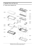
1
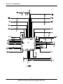
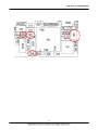
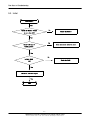
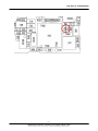
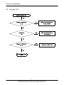
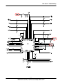
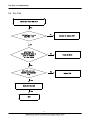
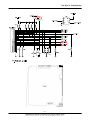
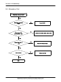
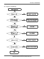
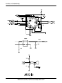
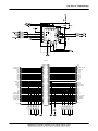
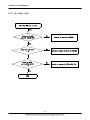
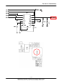
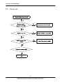
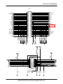
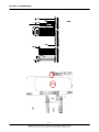
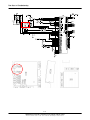
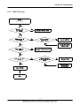
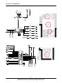
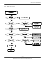
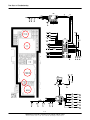
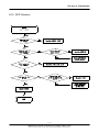
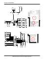
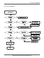
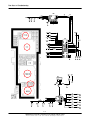
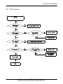
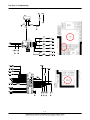
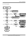
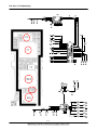
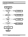
9. Flow Chart of Troubleshooting
9-1. Power On
' Power On ' does not work
Yes
Check the Battery Voltage
No
Change the Battery
is more than 3.5V
Yes
C403(+VDD_IO_LOW) &
C405(+VDD_IO_HIGH) = "H"
No
Change the PMIC(U403)
Yes
Check the Clock at
No
Resolder OSC400
R405=32KHz
Yes
C433(+VDD_GSM_CORE)
No
Check the +VDD_GSM_CORE circuit
= 1.2V
Yes
Check the initial operation
Yes
END
9-1
SAMSUNG Proprietary-Contents may change without notice
This Document can not be used without Samsung's authorization
Flow Chart of Troubleshooting
9-2
SAMSUNG Proprietary-Contents may change without notice
This Document can not be used without Samsung's authorization
Flow Chart of Troubleshooting
9-3
SAMSUNG Proprietary-Contents may change without notice
This Document can not be used without Samsung's authorization
Flow Chart of Troubleshooting
9-2. Initial
Initial Failure
Yes
No
Check the Battery Voltage
Change the Battery
is more than 3.5V
Yes
No
Check U403 pin 14
Check the circuit related to reset
(32KHz_DIGIT)
Yes
No
Is R224, R225
Check the U403
OK?
Yes
Check the 16bit data signal
Yes
END
9-4
SAMSUNG Proprietary-Contents may change without notice
This Document can not be used without Samsung's authorization
Flow Chart of Troubleshooting
9-5
SAMSUNG Proprietary-Contents may change without notice
This Document can not be used without Samsung's authorization
Flow Chart of Troubleshooting
9-3. Charging Part
Abnormal charging part
Yes
No
Check the U403 pin 38
Check the circuit related to
V_EXT_CHARGE
> 4.9V
Yes
No
U403 pin 34
Check the circuit related to
AUX_ON signal
= "L"
Yes
No
Check the U403 pin 46
Resolder or replace U403
≒ 1.4V
Yes
END
9-6
SAMSUNG Proprietary-Contents may change without notice
This Document can not be used without Samsung's authorization
Flow Chart of Troubleshooting
9-7
SAMSUNG Proprietary-Contents may change without notice
This Document can not be used without Samsung's authorization
Flow Chart of Troubleshooting
9-4. Sim Part
Phone can't access SIM Card
Yes
No
T/SIM500 pin 11 or 14
(SIM_VCC) = "H"
Resolder or replace U403
Yes
After Power ON,
No
Check SIMCLK Signal on
pin15 of T/SIM500
Check the Clock
in a few second
Yes
After SIM card insert,
No
T/SIM500 pin 13(SIMRST)
Replace PBA
= "H"
Yes
Check the SIM Card
Yes
END
9-8
SAMSUNG Proprietary-Contents may change without notice
This Document can not be used without Samsung's authorization
Flow Chart of Troubleshooting
9-9
SAMSUNG Proprietary-Contents may change without notice
This Document can not be used without Samsung's authorization
Flow Chart of Troubleshooting
9-5. Microphone Part
Microphone does not work
Yes
Check the connection
of MIC
No
Resolder MIC
Yes
Check the circuit
No
Resolder the TA602, R605, R608, R609
from UCP200 to MIC
Yes
Check F500, PIN 5
No
Check the JACK_IN signal
= "H"
Yes
No
Check the MIC
Replace the MIC
Yes
END
9-10
SAMSUNG Proprietary-Contents may change without notice
This Document can not be used without Samsung's authorization
Flow Chart of Troubleshooting
9-11
SAMSUNG Proprietary-Contents may change without notice
This Document can not be used without Samsung's authorization
Flow Chart of Troubleshooting
9-12
SAMSUNG Proprietary-Contents may change without notice
This Document can not be used without Samsung's authorization
Flow Chart of Troubleshooting
9-6. Speaker Part(Melody)
Speaker does not work
Yes
No
U601 pin 7 = 2.9V?
Resolder or replace U601
Yes
No
Check the Clock signal at
Check the clock generation circuit
(related to U101 and TCX100)
Pin 1 of TCX100(26MHz)
Yes
No
U601 pin 15,17 ≒ 1.8V
Resolder U601
(When U601 operating)
Yes
No
HCD500 pin 2,3 ≒ 1.8V?
Resolder HCD500
(When U601 operate)
No
Resolder or change L104
L104 pin 1, 2 ≒ 1.8V
Yes
No
Resolder of change the Speaker
Is the Speaker working?
Yes
END
9-13
SAMSUNG Proprietary-Contents may change without notice
This Document can not be used without Samsung's authorization
Flow Chart of Troubleshooting
9-14
SAMSUNG Proprietary-Contents may change without notice
This Document can not be used without Samsung's authorization
Flow Chart of Troubleshooting
9-7. Key Data Input
Check Initial Operation
Yes
When one of the keys is
No
pushed,
Check the Dome sheet & Key Pad
Isn't it displayed on LCD?
Yes
When one of the keys is
pushed,
No
Replace the PBA
KEY_ROW(0,4),
KEY_COL(0,4)
signal is OK?
Yes
END
9-15
SAMSUNG Proprietary-Contents may change without notice
This Document can not be used without Samsung's authorization
Flow Chart of Troubleshooting
9-8. Receiver Part
Receiver does not work
Yes
Check the U601
Pin 22, 23 (HFR_P, N)
= 1.4V
No
Resolder UCP200 or change PBA
Yes
Check the U601
Pin 15, 17(SPK_P, N)
= 1.8V
No
Resolder or replace the U601
Yes
No
Check the HCD500
Pin 2, 3 = 1.8V
Resolder or replace the HCD500
Yes
No
Check the soldering of the
speaker wire
Modify the speaker wire soldering
Yes
No
Is Receiver working ?
Replace the Speaker
Yes
END
9-16
SAMSUNG Proprietary-Contents may change without notice
This Document can not be used without Samsung's authorization
Flow Chart of Troubleshooting
HCD500
VIB
SLIDER_KEY_ON
RS
LCD_RESET
LD(15)
LD(14)
LD(13)
LD(12)
LD(11)
LD(10)
LD(9)
LD(8)
M_SCL
M_CLK
CAM_RESET
CAM_VDD_EN
Y(1)
Y(3)
Y(5)
Y(7)
VBAT
VBAT
+VDD_IO_HIGH
KEY_ROW(2)
KEY_ROW(3)
KEY_ROW(4)
FLM
SPK_P
C530
9-17
SAMSUNG Proprietary-Contents may change without notice
This Document can not be used without Samsung's authorization
C529
C527
9
7
5
3
1
C523
C522
C520
C521
C528
SPK_N
59
57
55
53
51
49
47
45
43
41
39
37
35
33
31
29
27
25
23
21
19
17
15
13
11
C526
8
6
4
2
59
57
55
53
51
49
47
45
43
41
39
37
35
33
31
29
27
25
23
21
19
17
15
13
11
9
7
5
3
1
C525
WHEEL_SW1
+VDD_WHEEL
KEY_COL(2)
KEY_COL(3)
KEY_COL(4)
VGH_DETECT
WHEEL_SW2
60
58
56
54
52
50
48
46
44
42
40
38
36
34
32
30
28
26
24
22
20
18
16
14
12
10
8
6
4
2
C524
60
58
56
54
52
50
48
46
44
42
40
38
36
34
32
30
28
26
24
22
20
18
16
14
12
10
BACKLIGHT
LCD_MAIN_CS
L_WR
LD(7)
LD(6)
LD(5)
LD(4)
LD(3)
LD(2)
LD(1)
LD(0)
ONKEY_N
M_SDA
P_CLK
HSYNC
VSYNC
Y(0)
Y(2)
Y(4)
Y(6)
Flow Chart of Troubleshooting
9-9. Back Light (for Color Main LCD)
Backlight does not work
Yes
No
Is LCD Contrast set on high
Set LCD Contrast on high level
level in the Menu?
Yes
Check the HCD500
pin 58 = H
No
Resolder HCD500 or change PBA
Yes
No
Check the SLC100
pin 58 = H
Resolder SLC100 or change SUB PBA
Yes
Change the LCD Module
Yes
END
9-18
SAMSUNG Proprietary-Contents may change without notice
This Document can not be used without Samsung's authorization
Flow Chart of Troubleshooting
HCD500
M_SCL
M_CLK
CAM_RESET
CAM_VDD_EN
Y(1)
Y(3)
Y(5)
Y(7)
VBAT
VBAT
+VDD_IO_HIGH
KEY_ROW(2)
KEY_ROW(3)
KEY_ROW(4)
FLM
SPK_P
C529
9
7
5
3
1
C524
C522
VIB
SLIDER_KEY_ON
RS
LCD_RESET
LD(15)
LD(14)
LD(13)
LD(12)
LD(11)
LD(10)
LD(9)
LD(8)
C523
C521
C520
C528
SPK_N
59
57
55
53
51
49
47
45
43
41
39
37
35
33
31
29
27
25
23
21
19
17
15
13
11
C527
8
6
4
2
59
57
55
53
51
49
47
45
43
41
39
37
35
33
31
29
27
25
23
21
19
17
15
13
11
9
7
5
3
1
C526
WHEEL_SW1
+VDD_WHEEL
KEY_COL(2)
KEY_COL(3)
KEY_COL(4)
VGH_DETECT
WHEEL_SW2
60
58
56
54
52
50
48
46
44
42
40
38
36
34
32
30
28
26
24
22
20
18
16
14
12
10
8
6
4
2
C525
60
58
56
54
52
50
48
46
44
42
40
38
36
34
32
30
28
26
24
22
20
18
16
14
12
10
BACKLIGHT
LCD_MAIN_CS
L_WR
LD(7)
LD(6)
LD(5)
LD(4)
LD(3)
LD(2)
LD(1)
LD(0)
ONKEY_N
M_SDA
P_CLK
HSYNC
VSYNC
Y(0)
Y(2)
Y(4)
Y(6)
C530
9-19
SAMSUNG Proprietary-Contents may change without notice
This Document can not be used without Samsung's authorization
Flow Chart of Troubleshooting
9-10. Key Back Light
Main Key LED does not work
Yes
Check the UCP200
related to "BACKLIGHT"
No
Resolder or change the UCP200
Yes
Check the U103 pin 2
= H
No
Check the U103
pin 5, 8(C112, C117)
= H
No
Resolder or change the U103 on Sub PBA
Resolder or change the U103 on Sub PBA
Yes
END
9-20
SAMSUNG Proprietary-Contents may change without notice
This Document can not be used without Samsung's authorization
Flow Chart of Troubleshooting
9-21
SAMSUNG Proprietary-Contents may change without notice
This Document can not be used without Samsung's authorization
Flow Chart of Troubleshooting
9-11. Camera part
"Camera" function does not work
Yes
No
Check the Camera
Reconnect the camera module
connector on Sub PBA
Yes
No
HCD500 Pin 27 = H
Resolder HCD500 or change PBA
Yes
No
R336 or SLC101 pin 8
= 32MHz
Check U302 related to 32MHz
Yes
Replace the camera module
END
9-22
SAMSUNG Proprietary-Contents may change without notice
This Document can not be used without Samsung's authorization
Flow Chart of Troubleshooting
HCD500
M_SCL
M_CLK
CAM_RESET
CAM_VDD_EN
Y(1)
Y(3)
Y(5)
Y(7)
VBAT
VBAT
+VDD_IO_HIGH
KEY_ROW(2)
KEY_ROW(3)
KEY_ROW(4)
FLM
SPK_P
C529
9
7
5
3
1
C523
C522
C521
C520
C528
SPK_N
VIB
SLIDER_KEY_ON
RS
LCD_RESET
LD(15)
LD(14)
LD(13)
LD(12)
LD(11)
LD(10)
LD(9)
LD(8)
C527
8
6
4
2
59
57
55
53
51
49
47
45
43
41
39
37
35
33
31
29
27
25
23
21
19
17
15
13
11
C526
WHEEL_SW1
+VDD_WHEEL
KEY_COL(2)
KEY_COL(3)
KEY_COL(4)
VGH_DETECT
WHEEL_SW2
59
57
55
53
51
49
47
45
43
41
39
37
35
33
31
29
27
25
23
21
19
17
15
13
11
9
7
5
3
1
C525
BACKLIGHT
LCD_MAIN_CS
L_WR
LD(7)
LD(6)
LD(5)
LD(4)
LD(3)
LD(2)
LD(1)
LD(0)
ONKEY_N
M_SDA
P_CLK
HSYNC
VSYNC
Y(0)
Y(2)
Y(4)
Y(6)
60
58
56
54
52
50
48
46
44
42
40
38
36
34
32
30
28
26
24
22
20
18
16
14
12
10
8
6
4
2
C524
60
58
56
54
52
50
48
46
44
42
40
38
36
34
32
30
28
26
24
22
20
18
16
14
12
10
C530
9-23
SAMSUNG Proprietary-Contents may change without notice
This Document can not be used without Samsung's authorization
Flow Chart of Troubleshooting
9-24
SAMSUNG Proprietary-Contents may change without notice
This Document can not be used without Samsung's authorization
Flow Chart of Troubleshooting
9-12. BLUETOOTH
BLUETOOTH does not work
Yes
No
RTS2, TXD2
(TP106, TP107) = H
Resolder U102 or Replace UCP200
Yes
No
Check ANT102
Replace ANT102
Yes
END
9-25
SAMSUNG Proprietary-Contents may change without notice
This Document can not be used without Samsung's authorization
Flow Chart of Troubleshooting
9-26
SAMSUNG Proprietary-Contents may change without notice
This Document can not be used without Samsung's authorization
Flow Chart of Troubleshooting
9-13. GSM Receiver
RX ON
RF input : 62CH
Amp : -50dBm
Yes
No
MOD100 pin8
>= -65dBm
Resolder CNS100, C102
Yes
MOD100 pin1, 2
>= -65dBm
No
Check MOD100
pin10, 12 = L
No
Yes
Yes
U101 pin27, 28
>= -70dBm
No
Resolder MOD100
Check ANT Switch
control circuit
Resolder L113, L114, L115
Yes
U101 pin1, 2, 3, 4
>= 1V
No
Check U101 pin
5, 15, 17, 20, 31, 38
>=2.7V
Yes
No
Yes
Check UCP200
END
9-27
SAMSUNG Proprietary-Contents may change without notice
This Document can not be used without Samsung's authorization
Resolder U101
Check or resolder
TCX100(26MHz),
RF PSU Part
Flow Chart of Troubleshooting
9-28
SAMSUNG Proprietary-Contents may change without notice
This Document can not be used without Samsung's authorization
Flow Chart of Troubleshooting
9-14. GSM Transmitter
TX ON (5Level)
Yes
No
MOD100 pin8
>= 20dBm
Resolder CN100, C102
Yes
MOD100 pin13
>= 18dBm
No
Check MOD100
pin12 = H and
pin10 = L
No
Change or Resolder
MOD100
Yes
Yes
PAM100 pin12
>= 18dBm
No
Check ANT Switch
control circuit
Resolder C107, L111
Yes
PAM100 pin7
>= -11dBm
No
Check PAM100
pin4, pin6 = H
No
Check VBAT or PAM100
control signal
Yes
Yes
U101 pin1, 2, 3, 4
>= 1V
No
Check U101 pin
5, 15, 17, 20, 31, 38
>=2.7V
Yes
Resolder or Change PAM100
No
Yes
Check UCP200
END
9-29
SAMSUNG Proprietary-Contents may change without notice
This Document can not be used without Samsung's authorization
Resolder U101
Check & Resolder
U101, TCX100
(26MHz), RF PSU Part
Flow Chart of Troubleshooting
9-30
SAMSUNG Proprietary-Contents may change without notice
This Document can not be used without Samsung's authorization
Flow Chart of Troubleshooting
9-15. DCS Receiver
RX ON
RF input : 698CH
Amp : -50dBm
Yes
No
MOD100 pin8
>= -65dBm
Resolder CN100, C102
Yes
MOD100 pin3, 4
>= -65dBm
No
Check MOD100
pin10, 12 = L
No
Yes
Yes
U101 pin24, 25
>= -70dBm
No
Resolder MOD100
Check ANT Switch
control circuit
Resolder L107, L108, L112
Yes
U101 pin1, 2, 3, 4
>= 1V
No
Check U101 pin
5, 15, 17, 20, 31, 38
>=2.7V
No
Yes
Yes
Check UCP200
END
9-31
SAMSUNG Proprietary-Contents may change without notice
This Document can not be used without Samsung's authorization
Resolder U101
Check &Resolder
TCX100(26MHz),
RF PSU Part
Flow Chart of Troubleshooting
9-32
SAMSUNG Proprietary-Contents may change without notice
This Document can not be used without Samsung's authorization
Flow Chart of Troubleshooting
9-16. DCS Transmitter
TX ON (0Level)
Yes
No
MOD100 pin8
>= 20dBm
Resolder CN100, C102
Yes
No
MOD100 pin11
>= 18dBm
Check MOD100
pin12 = L,
pin10 = H
No
Yes
Yes
No
PAM100 pin18
>= 18dBm
Check ANT Switch
control circuit
Change or Resolder MOD100
Resolder C108, C112, L110
Yes
No
PAM100 pin1
>= -11dBm
Check PAM100
pin4, 6 = H
No
Resolder or Change PAM100
Check +VBAT or PAM100
control signal
Yes
Yes
U101 pin1, 2, 3, 4
>= 1V
No
Check U101 pin
5, 15, 17, 20, 31, 38
>=2.7V
No
Yes
Yes
Check UCP200
END
9-33
SAMSUNG Proprietary-Contents may change without notice
This Document can not be used without Samsung's authorization
Check & Resolder
TCX100(26MHz),
RF PSU Part
Resolder U101
Flow Chart of Troubleshooting
9-34
SAMSUNG Proprietary-Contents may change without notice
This Document can not be used without Samsung's authorization
Flow Chart of Troubleshooting
9-17. PCS Receiver
RX ON
RF input : 661CH
Amp : -50dBm
Yes
No
MOD100 pin8
>= -65dBm
Resolder CN100, C102
Yes
MOD100 pin5, 6
>= -65dBm
No
Check MOD100
pin10, 12 = L
No
Yes
Yes
U101 pin22, 23
>= -70dBm
No
Resolder MOD100
Check ANT Switch
control circuit
Resolder L104, L105, L106
Yes
U101 pin1, 2, 3, 4
>= 1V
No
Check U101 pin
5, 15, 17, 20, 31, 38
>=2.7V
No
Yes
Yes
Check UCP200
END
9-35
SAMSUNG Proprietary-Contents may change without notice
This Document can not be used without Samsung's authorization
Resolder U101
Check & Resolder
TCX100(26MHz),
RF PSU Part
Flow Chart of Troubleshooting
9-36
SAMSUNG Proprietary-Contents may change without notice
This Document can not be used without Samsung's authorization
Flow Chart of Troubleshooting
9-18. PCS Transmitter
TX ON (0Level)
Yes
No
MOD100 pin8
>= 20dBm
Resolder CN100, C102
Yes
MOD100 pin11
>= 18dBm
No
Check MOD100
pin12 = L,
pin10 = H
No
Change or Resolder MOD100
Yes
Yes
PAM100 pin18
>= 18dBm
No
Check ANT Switch
control circuit
Resolder C108, C112, L110
Yes
No
PAM100 pin1
>= -11dBm
Check PAM100
pin4, 6 = H
No
Check +VBAT or PAM100
control signal
Yes
Yes
Resolder or Change PAM100
U101 pin1, 2, 3, 4
>= 1V
No
Check U101 pin
5, 15, 17, 20, 31, 38
>=2.7V
Yes
No
Yes
Check UCP200
END
9-37
SAMSUNG Proprietary-Contents may change without notice
This Document can not be used without Samsung's authorization
Resolder U101
Check & Resolder
TCX100(26MHz),
RF PSU Part
Flow Chart of Troubleshooting
9-38
SAMSUNG Proprietary-Contents may change without notice
This Document can not be used without Samsung's authorization