1
Introduction
Xilinx Blockset Overview
Xilinx Blocks
System Generator Software Features
Xilinx System
Generator v2.1 for
Using the Xilinx Software
Auxiliary Files
Simulink
User Guide
Xilinx Blockset
Reference Guide
—
Printed in U.S.A.
Xilinx System Generator v2.1 Reference Guide
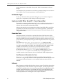
About This Manual
This document is a reference guide for system designers who are unfamiliar with the
System Generator v2.1 and the Xilinx Blockset.
Manual Contents
This guide covers the following topics:
2
•
Chapter 1, Introduction, gives a high-level overview of the System Generator and
its uses.
•
Chapter 2, Xilinx Blockset Overview, describes the Xilinx Blockset: how to
instantiate a Xilinx block within your Simulink model, how to configure it
through its block parameters dialog box, the common options that can be used in
several of the blocks, and the nature of the signals used in the System Generator
software.
•
Chapter 3, Xilinx Blocks, describes the details of each block, including options, and
use of Xilinx LogiCOREs. This chapter also tells where to find descriptions of
the cores on your computer.
•
Chapter 4, System Generator Software Features, describes the System Generator
software and gives tips for using it to create efficient hardware designs.
•
Chapter 5, Using the Xilinx Software, tells, step-by-step, how to use System
Generator as a front-end to the Xilinx Foundation 4.1i ISE software, from VHDL
to bitstream generation.
•
Chapter 6, Auxiliary Files, contains instructions for accessing System Generator
demo designs, as well as a list of Perl scripts that are delivered with the System
Generator software. The demo designs show examples of designs using Xilinx
blocks. The scripts are used by the System Generator to create auxiliary project
files, but can also be used as stand-alone tools.
Xilinx Development System
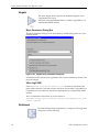
Additional Resources
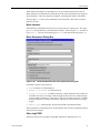
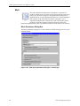
For additional information, go to http://support.xilinx.com. The following
table lists some additional resources.
Resource
Description/URL
IP Center
Information on Xilinx LogiCOREs and IP solutions.
http://www.xilinx.com/ipcenter/
This page contains a link to the Xilinx Xtreme DSP solutions page.
Technical Tips
Latest news, design tips, and patch information for the Xilinx design environment.
http://support.xilinx.com/xlnx/xil_tt_home.jsp
Tutorials
Tutorials covering Xilinx ISE 4.1i design flows, from design entry to verification and
debugging.
http://support.xilinx.com/support/techsup/tutorials/
tutorials4.htm
Documentation
Xilinx Software Manuals online.
http://toolbox.xilinx.com/docsan/xilinx4/
Software
Updates
Periodic software service packs, IP updates, and information is available online.
http://support.xilinx.com/support/software/install_info.htm
The
MathWorks
MATLAB , Simulink , DSP design, and other company information.
http://www.mathworks.com
3
Xilinx System Generator v2.1 Reference Guide
Conventions
This document uses the following conventions. An example illustrates each
convention.
Typographical
The following conventions are used for all System Generator documents.
•
Courier font (a fixed-width font) indicates messages, prompts, menu pick
items, and dialog box entries that the system displays.
speed grade: - 100
•
Courier bold indicates literal commands that you enter in a command-line
prompt or dialog box. However, triangular braces “<>” in Courier bold are not
literal.
>> cd <your $MATLAB home directory>
•
Italic font denotes the following items.
♦
Introduction of words being used with a context-specific definition
The System Generator provides bit true and cycle true modeling.
♦
References to other manuals or sections in this manual
See the Development System Reference Guide for more information.
♦
Emphasis in text
If a wire is drawn so that it overlaps the pin of a symbol, the two nets are not
connected.
4
Xilinx Development System
Contents
Chapter 1
Introduction
Industry and Product Overview .................................................................................8
System Generator .....................................................................................................9
System Level Modeling with System Generator .......................................................9
The System Generator Design Flow .........................................................................10
Arithmetic Data Types ..............................................................................................12
Hardware Handshaking ............................................................................................13
Multirate Systems ................................................................................................13
Bit-True and Cycle-True Modeling ............................................................................14
Automatic Testbench Generation ........................................................................14
Chapter 2
Xilinx Blockset Overview
What is a Xilinx Block? .............................................................................................15
Instantiating Xilinx Blocks within a Simulink Model ...................................................16
The Block Parameters Dialog Box ............................................................................16
The Nature of Signals in the Xilinx Blockset .............................................................16
Use of Xilinx Smart-IP Cores by the System Generator ...........................................18
Licensed Cores ....................................................................................................18
Xilinx LogiCORE Versions ...................................................................................19
Common Options in Block Parameters Dialog Box ..................................................19
Arithmetic Type ....................................................................................................20
Implement with Xilinx Smart-IP Core (if possible) ...............................................20
Generate Core .....................................................................................................20
Latency ................................................................................................................20
Precision ..............................................................................................................21
Number of Bits .....................................................................................................21
Overflow and Quantization ..................................................................................21
Override with Doubles .........................................................................................21
Sample Period .....................................................................................................22
Chapter 3
Xilinx Blocks
Basic Elements .........................................................................................................23
System Generator ...............................................................................................23
Addressable Shift Register ..................................................................................26
Black Box .............................................................................................................28
5
Xilinx System Generator v2.1 Reference Guide
Concat .................................................................................................................30
Constant ..............................................................................................................31
Convert ................................................................................................................31
Counter ................................................................................................................32
Delay ...................................................................................................................35
Down Sample ......................................................................................................36
Get Valid Bit .........................................................................................................37
Mux ......................................................................................................................38
Parallel to Serial ..................................................................................................39
Register ...............................................................................................................40
Reinterpret ...........................................................................................................42
Serial to Parallel ..................................................................................................43
Set Valid Bit .........................................................................................................45
Slice .....................................................................................................................45
Sync .....................................................................................................................47
Up Sample ...........................................................................................................50
Communication .........................................................................................................52
Convolutional Encoder ........................................................................................52
Depuncture ..........................................................................................................54
Interleaver Deinterleaver .....................................................................................55
Puncture ..............................................................................................................58
RS Decoder .........................................................................................................59
RS Encoder .........................................................................................................63
Viterbi Decoder ....................................................................................................68
DSP ..........................................................................................................................70
CIC ......................................................................................................................70
DDS .....................................................................................................................73
FFT ......................................................................................................................75
FIR .......................................................................................................................79
Math ..........................................................................................................................81
Accumulator .........................................................................................................81
AddSub ................................................................................................................83
CMult ...................................................................................................................84
Inverter ................................................................................................................85
Logical .................................................................................................................86
Mult ......................................................................................................................88
Negate .................................................................................................................90
Relational .............................................................................................................90
Scale ....................................................................................................................92
Shift .....................................................................................................................92
SineCosine ..........................................................................................................93
Threshold .............................................................................................................95
MATLAB I/O ..............................................................................................................96
Gateway Blocks ...................................................................................................96
Enabled Subsystems ...........................................................................................96
Gateway In ...........................................................................................................97
6
Xilinx Development System
Gateway Out.........................................................................................................99
Quantization Error Blocks ....................................................................................101
Display .................................................................................................................101
Memory .....................................................................................................................102
Dual Port RAM .....................................................................................................102
FIFO ....................................................................................................................106
ROM ....................................................................................................................107
Single Port RAM ..................................................................................................110
State Machine ...........................................................................................................114
Mealy State Machine ...........................................................................................114
Moore State Machine ..........................................................................................116
Registered Mealy State Machine .........................................................................119
Registered Moore State Machine ........................................................................123
Chapter 4
System Generator Software Features
Using the System Generator installer .......................................................................127
Uninstalling previous System Generator directories ............................................127
Installed System Generator directory ..................................................................128
Using Black Boxes ....................................................................................................128
Example model ....................................................................................................128
Black Box window ................................................................................................129
Use of mixed language projects ...............................................................................130
Incorporating mixed language black boxes .........................................................130
Tips for creating a high performance design ............................................................132
Using the System Generator Constraints Files..........................................................133
System Clock Period ............................................................................................133
Multicycle Path Constraints ..................................................................................133
IOB Timing and Placement Constraints ...............................................................134
Example for showing constraints use ...................................................................134
Important Issues ...................................................................................................136
Files automatically created by System Generator ....................................................137
Chapter 5
Using the Xilinx Software
Xilinx ISE 4.1i Project Navigator ...............................................................................139
Opening a System Generator project ..................................................................139
Customizing your System Generator project .......................................................139
Implementing your design ...................................................................................140
Simulating using ModelSim within the Project Navigator ....................................141
Using an EDIF software flow ....................................................................................143
Simulation .................................................................................................................143
Compiling your IP ................................................................................................143
Associating ModelSim with ISE 4.1i Project Navigator ........................................144
Xilinx software tools resources .................................................................................145
Chapter 6
Auxiliary Files
Demonstration designs ..............................................................................................146
Perl scripts .................................................................................................................147
7
Xilinx System Generator v2.1 Reference Guide
Chapter 1
Introduction
This chapter describes the basic concepts and tools of the System Generator v2.1.
This chapter contains the following sections.
•
Industry and Product Overview
•
System Generator
•
System Level Modeling with System Generator
•
The System Generator Design Flow
•
Arithmetic Data Types
•
Hardware Handshaking
•
Bit-true and Cycle-true Modeling
Industry and Product Overview
In recent years, field-programmable gate arrays (FPGAs) have become key
components in implementing high performance digital signal processing (DSP)
systems, especially in the areas of digital communications, networking, video, and
imaging. The logic fabric of today's FPGAs consists not only of look-up tables,
registers, multiplexers, distributed and block memory, but also dedicated circuitry for
fast adders, multipliers, and I/O processing (e.g., giga-bit I/O). The memory
bandwidth of a modern FPGA far exceeds that of a microprocessor or DSP processor
running at clock rates two to ten times that of the FPGA. Coupled with a capability
for implementing highly parallel arithmetic architectures, this makes the FPGA
ideally suited for creating high-performance custom data path processors for tasks
such as digital filtering, fast Fourier transforms, and forward error correction.
For example, all major telecommunication providers have adopted FPGAs for highperformance DSP out of necessity. A third-generation (3G) wireless base station
typically contains FPGAs and ASICs in addition to microprocessors and digital signal
processors (DSPs). The processors and DSPs, even when running at GHz clock rates,
are increasingly used for relatively low MIPs packet level processing, with the chip
and symbol rate processing being implemented in the FPGAs and ASICs. The fluidity
of emerging standards often makes FPGAs, which can be reprogrammed in the field,
better suited than ASICs.
Despite these characteristics, broader acceptance of FPGAs in the DSP community has
historically been hampered by several factors. First, there is a general lack of
familiarity with hardware design and especially, FPGAs. DSP engineers conversant
with programming in C or assembly language are often unfamiliar with digital design
using hardware description languages (HDLs) such as VHDL or Verilog.
Furthermore, although VHDL provides many high level abstractions and language
8
Xilinx Development System
Introduction
constructs for simulation, its synthesizable subset is far too restrictive for system
design.
System Generator is a software tool for modeling and designing FPGA-based DSP
systems in Simulink. The tool presents a high level abstract view of a DSP system, yet
nevertheless automatically maps the system to a faithful hardware implementation.
What is most significant is that System Generator provides these services without
substantially compromising either the quality of the abstract view or the performance
of the hardware implementation.
System Generator
Simulink provides a powerful high level modeling environment for DSP systems, and
consequently is widely used for algorithm development and verification. System
Generator maintains an abstraction level very much in keeping with the traditional
Simulink blocksets, but at the same time automatically translates designs into
hardware implementations that are faithful, synthesizable, and efficient.
The implementation is faithful in that the system model and hardware
implementation are bit-identical and cycle-identical at sample times defined in
Simulink. The implementation is made efficient through the instantiation of
intellectual property (IP) blocks that provide a range of functionality from arithmetic
operations to complex DSP functions. These IP blocks have been carefully designed
to run at high speed and to be area efficient. In System Generator, the capabilities of
IP blocks have been extended transparently and automatically to fit gracefully into a
system level framework. For example, although the underlying IP blocks operate on
unsigned integers, System Generator allows signed and unsigned fixed point
numbers to be used, including saturation arithmetic and rounding. User-defined IP
blocks can be incorporated into a System Generator model as black boxes which will
be embedded by the tool into the HDL implementation of the design.
System Level Modeling with System Generator
The creation of a DSP design begins with a mathematical description of the operations
needed and concludes with a hardware realization of the algorithm. The hardware
implementation is rarely faithful to the original functional description --instead it is
faithful enough. The challenge is to make the hardware area and speed efficient while
still producing acceptable results.
In a typical design flow --a flow supported by System Generator-- the following steps
occur:
1.
Describe the algorithm in mathematical terms,
2.
Realize the algorithm in the design environment, initially using double precision,
3.
Trim double precision arithmetic down to fixed point,
4.
Translate the design into efficient hardware.
Step 4 is error prone because it can be difficult to guarantee the hardware implements
the design faithfully. System Generator eliminates this concern by automatically
generating a faithful hardware implementation.
Step 3 is error prone because an efficient hardware implementation uses just enough
fixed point precision to give correct results. System Generator does not automate this
step, which typically involves subtle trade off analysis, but it does provide tools to
make the process tractable. You might wonder why it is not possible to eliminate Step
System Generator
9
Xilinx System Generator v2.1 Reference Guide
3 and simply use floating point operations in hardware. The answer is that most
operations have a sufficiently small dynamic range that a fixed point representation is
acceptable, and the hardware realization of fixed point is considerably cheaper.
The System Generator Design Flow
Simulink provides a graphical environment for creating and modeling dynamical
systems. System Generator consists of a Simulink library called the Xilinx Blockset,
and software to translate a Simulink model into a hardware realization of the model.
System Generator maps system parameters defined in Simulink (e.g. as mask
variables in Xilinx Blockset blocks), into entities and architectures, ports, signals, and
attributes in a hardware realization. In addition, System Generator automatically
produces command files for FPGA synthesis, HDL simulation, and implementation
tools, so that the user can work entirely in graphical environments in going from
system specification to hardware realization.
10
Xilinx Development System
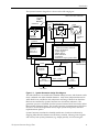
Introduction
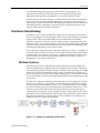
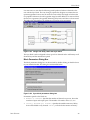
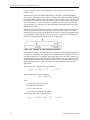
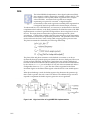
The System Generator design flow is shown in the following figure.
MATLAB Environment
Library
(including
Xilinx
Blockset)
Simulink
System Model
Simulation
Input
Output
+
Z
–1
k
including
S-functions
Simulation
Data
Synthesis
System Generator
Code Generation Software
- map to IP libraries
- control signals
- VHDL design
- HDL testbench
- constraints
- simulation scripts, project files
ENTITY mult IS
GENERIC(w:
PORT(a,b:IN
PORT(y:OUT
END ENTITY
...
VHDL
Synthesis
Compiler
Xilinx
DesignTools
Environment
Core
Parameters
CORE
Generator
Test
Vectors
EDIF
FPGA
Place & Route
EDIF + Timing
Bit stream
Logic
Simulator
Pass/Fail
Figure 1-1: System Generator design flow diagram
The Xilinx Blockset is accessible in the Simulink library browser, and elements can be
freely combined with other Simulink elements. Only those subsystems denoted as
Xilinx black boxes, and blocks and subsystems consisting of blocks from the Xilinx
Blockset are translated by System Generator into a hardware realization. The
generation process is controlled from the System Generator block found in the Xilinx
Blockset Basic Elements library. The System Generator parameterization GUI allows
the user to choose the target FPGA device, target system clock period, and other
implementation options.
System Generator translates the Simulink model into a hardware realization by
mapping Xilinx Blockset elements into IP library modules, inferring control signals
and circuitry from system parameters (e.g. sample periods), and converting the
The System Generator Design Flow
11
Xilinx System Generator v2.1 Reference Guide
Simulink hierarchy into a hierarchical VHDL netlist. In addition, System Generator
creates the necessary command files to create the IP block netlists using CORE
Generator, invokes CORE Generator, and creates project and script files for HDL
simulation, synthesis, technology mapping, placement, routing, and bit stream
generation. To ensure efficient compilation of multi-rate systems, System Generator
creates constraint files for the physical implementation tools. System Generator also
creates an HDL test bench for the generated realization, including test vectors
computed during Simulink simulation.
Arithmetic Data Types
System Generator provides the three arithmetic data types that are of greatest use in
DSP: double precision floating point, and signed and unsigned fixed point numbers.
Floating point data cannot be converted into hardware, but is supported for
simulation and modeling.
The set of signed arbitrary precision fixed point numbers has nice mathematical
properties, allowing for operations that are much cleaner than those on familiar
floating point representations. Operations on floating point numbers entail implicit
rounding on the result, and consequently, desirable algebraic characteristics such as
associativity and distributivity are lost. Both are retained for arbitrary precision fixed
point numbers.
System Generator allows the quantization of the design to be addressed as an issue
separate from the implementation of the mathematical algorithm. The transition from
double precision to fixed point can be done selectively. In practice this means the
designer gets the design working using double precision, then converts to fixed point
incrementally. At all times, these three representations can be freely intermingled
without any changes to the signal flow graph. This mixing is possible because library
building blocks are polymorphic, changing their internal behavior based on the types
of their inputs.
There is another benefit from this scheme in which quantization events are broken out
as separate design parameters. At every point and stage of the design, the designer
can specify how both the overflow and the rounding issues are to be addressed. For
cases of overflow, the designer can choose whether or not saturation should be
applied, and do so in consideration of the hardware cost versus the benefit to the
system design. Saturation is a more faithful reflection of the underlying mathematics,
but more expensive in hardware; wrapping is inexpensive but less faithful. It is also
possible to trap overflow events in the system level simulation, which can be a useful
debugging mechanism in the design of subsystem that are intended never to result in
overflow.
Likewise, when quantizing at the least significant bit, the designer can choose
whether the value should be truncated (with no hardware cost) or rounded under
some particular rule (possibly improving the system design, but with added cost in
hardware).
In System Generator, many operators support full precision outputs, which means that
the output precision is always sufficient to carry out the operation without loss
information. Combined with the data type propagation rules supported in Simulink,
this allows great convenience when designing an algorithm. Naturally, any operator
that increases the output width of its inputs (e.g. an adder) cannot feed back on itself
with full precision.
The designer specifies the translation to fixed precision at key points in the design (in
particular, at gateways from the outside world and in feedback loops), and System
12
Xilinx Development System
Introduction
Generator then propagates signal types and precisions as appropriate. The
automatically chosen type is the least expensive that preserves full precision.
Translations from signed to unsigned and vice versa are automatic as well.
System Generator also allows designs to contain elements that cannot be realized in
hardware, but assist development and debugging. Examples of such elements are
signal sources, scopes, and machinery that tracks the divergence between fixed point
and double precision calculations. System Generator automatically discards such
elements when asked to translate to hardware.
Hardware Handshaking
In Simulink, time evolution is defined by sample rates for each block in the system.
There are propagation rules along signals so that not every block need set an explicit
sample period. This is extremely flexible, but has implications for modeling
hardware. Sequential circuits are clocked, and a key aspect of designing, especially
multirate systems, is the interplay between clock and clock enable signals. Although
abstracted, a bit and cycle true simulation must have mechanisms for defining and
controlling clocked behavior in the system model.
Every signal has a fixed point value as defined in the previous section. In addition, it
carries an implicit boolean valid bit that can be used to achieve hardware handshakes
between blocks. For example, upon startup, a pipeline may define its output invalid
until it has flushed its pipe. By inspecting the valid bits of its inputs, a block can
determine how to process its input data.
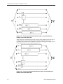
Multirate Systems
Multirate systems can be implemented in System Generator by using sample rate
conversion blocks for up-sampling and down-sampling. The necessary control logic
is automatically generated when the design is netlisted. Before netlisting, the sample
rates in the system are normalized to integer values; in hardware, the system clock
period corresponds to the GCD of the integer sample periods. Clock enables are used
to activate the hardware blocks at the appropriate moment in time with respect to the
system clock.
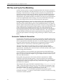
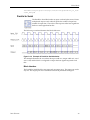
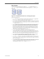
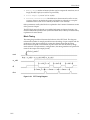
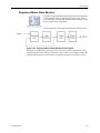
Consider for example, the multirate system model shown in the figure below, which
consists of I/O registers, an up-sampler, an anti-aliasing filter, and a down-sampler.
The input signal is up-sampled by a factor of two, and subsequently down-sampled
by a factor of three, giving an overall sample rate conversion by a factor of 2/3. The
ST blocks in the system model extract the sample period from a Simulink signal,
which can then be displayed. In the example, the input sample period is one. In the
generated hardware implementation shown below the system model, each element is
driven by the system clock, with its respective clock enable driven according to its
sample period in the original system model.
Figure 1-2: Example of a multirate system model
Hardware Handshaking
13
Xilinx System Generator v2.1 Reference Guide
Bit-True and Cycle-True Modeling
System Generator produces a hardware implementation that is bit and cycle true to
the system level simulation. We define the term bit and cycle true at the boundaries of
the design. The boundaries of a design in System Generator are specified by the
presence of Gateway In and Gateway Out blocks. These form interfaces between data
representation within System Generator and data types that can be examined and
manipulated in the standard Simulink environment. The gateways are translated into
ports in the implemented hardware design. The Gateway In blocks become input
ports to the design and the Gateway Out blocks become output ports.
In the Simulink simulation, Gateway in and Out blocks have data samples flowing
through at regular sample periods. The values flowing in provide the stimuli, and
those flowing out represent the response. In the generated hardware, if an identical
stimulus sequence is presented at the input ports (at clock events corresponding to the
input sample periods), then identical output sequences will be observed (here at clock
events corresponding to Simulink output events). The values presented to the
hardware input ports and produced by the output ports are bit vectors interpreted as
representing the fixed point values of the Simulink simulation. This correspondence
between Simulink and hardware results is guaranteed to hold regardless of the
particular input stimulus to the design or the positioning or number of Gateway Out
blocks.
Automatic Testbench Generation
For a black box instantiation, the design must provide both a Simulink model and an
implementation. System Generator cannot automatically provide the verification that
the two representations of the black box match. To assist the designer in verifying that
the system model simulated in Simulink mirrors the generated hardware circuit, a
VHDL test bench is automatically created during HDL code generation.
Test bench input stimuli are recorded by Gateway In blocks during Simulink
simulation. These blocks quantize double precision input date into a fixed point
representation. The fixed point values are saved to a data file and then used as input
stimuli during VHDL simulation.
Gateway Out blocks convert the fixed point representation into Simulink floating
point and define the output data ports of the HDL design. The signal connected to the
input of a Gateway In block is sampled at a given sample rate and is used as expected
data in the HDL simulation.
During HDL code generation, each Gateway In block is translated to a VHDL
component which reads the input stimuli. Gateway Out blocks are translated to
components that compare the VHDL results to the expected results. The comparisons
are performed at the blocks' sample rates. Only values which are tagged as valid by
the valid bit are compared.
The fixed point data type in Simulink is represented using a std_logic_vector in
VHDL. The position of the binary point, size of the container, and treatment of sign
are supplied to the VHDL as generic parameters. To ease the interpretation of fixed
point types in VHDL, the Gateway In and Out blocks convert the
std_logic_vector into a real number representation by using the generic
parameter information. A sequence of real numbers can then be viewed as an analog
waveform in an HDL simulator.
14
Xilinx Development System
Xilinx Blockset Overview
Chapter 2
Xilinx Blockset Overview
This chapter gives an overview of the Xilinx Blockset, including background
information on underlying blockset implementation, which will help you understand
how each block can be used to create and simulate your designs.
This chapter contains the following sections.
•
What is a Xilinx Block?
•
Instantiating Xilinx Blocks Within a Simulink Model
•
The Block Parameters Dialog Box
•
The Nature of Signals in the Xilinx Blockset
•
Use of Xilinx Smart-IP Cores by the System Generator
•
Common Options in Xilinx Block Parameters Dialog Box
What is a Xilinx Block?
The Xilinx Blockset is a Simulink
library, accessible from the Simulink
library browser. It consists of building
blocks that can be instantiated within
a Simulink model and, like other
Simulink blocksets, blocks can be
combined to form subsystems and
arbitrary hierarchies. The Xilinx
Gateway blocks (from the Xilinx
Blockset’s MATLAB I/O library) are
used to interface between the Xilinx
Blockset fixed point data type and
other Simulink blocks.
Every Xilinx Block can be configured
using a block parameters dialog box, with
few exceptions even during
simulation. Many blocks share
common parameters, which are
described later in this chapter. Most
also have parameters specific to the
function computed.
The System Generator is able to
generate an FPGA implementation consisting of RTF VHDL and Xilinx Smart-IP
Cores from a Simulink subsystem built from the Xilinx Blockset. The overall design,
including test environment, may consist of arbitrary Simulink blocks. However, the
What is a Xilinx Block?
15
Xilinx System Generator v2.1 Reference Guide
portion of a Simulink model to be implemented in an FPGA must be built exclusively
of Xilinx blocks, with the exception of subsystems denoted as black boxes.
Instantiating Xilinx Blocks within a Simulink Model
Xilinx blocks can be dragged (from the Simulink library browser, or from an
expanded sheet showing the blocks in the library) and dropped onto a Simulink
model sheet. Double-clicking on a block icon will open its block parameters dialog
box and allow customization of that instance of the block. It is also possible to build
user libraries of customized blocks and subsystems. Refer to the manual: Using
Simulink from The MathWorks.
The Xilinx blocks operate on fixed point data, using an arbitrary precision arithmetic
type. The Gateway blocks found in the Xilinx MATLAB I/O library comprise the
interface between Xilinx blocks and other Simulink blocks, and enable Xilinx blocks to
be freely instantiated within a Simulink model. Of course, the only blocks that System
Generator will convert to hardware are those from the Xilinx Blockset.
The Block Parameters Dialog Box
Most Xilinx blocks have parameters that can be configured. The typical block has a
dialog box with several common parameters (common to most blocks in the blockset)
and some specific parameters (specific to the particular block only). Double-clicking
on any block icon on a sheet will open its block parameters dialog box. Details of the
use of each block’s parameters dialog can be found elsewhere in this document.
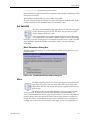
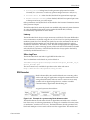
Each parameters dialog contains four buttons: OK, Cancel, Help, and Apply.
Apply applies your configuration changes to the block, leaving the box still visible on
your screen. Help launches HTML help information for the block. Cancel closes the
box without saving any changes, and OK applies your configuration changes and
closes the box.
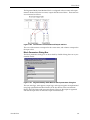
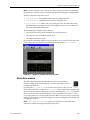
Figure 2-1: Buttons common to each block parameters dialog box
The Nature of Signals in the Xilinx Blockset
The fundamental scalar signal type in Simulink is double precision floating point. In
contrast, for bit and cycle true simulation of hardware, System Generator signals are
represented in an arbitrary precision fixed point arithmetic type. The Xilinx Gateway
In block converts double precision values into fixed point, and the Gateway Out
block converts fixed point values back into double precision floating point.
Some blocks produce full precision values by default, which is to say their output
signal has sufficient precision to represent the output without rounding error or
overflow. Some blocks also support the option of defining the output precision to be a
specific arithmetic type (e.g., 16-bit signed data with 8 bits of fraction), with
quantization options of rounding or truncation, and with overflow options of
saturation or truncation.
16
Xilinx Development System
Xilinx Blockset Overview
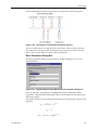
As an example, the figures shown below depict the Xilinx Negate block parameters
dialog box with full and user defined precision. Note in the latter case the additional
options for selecting quantization and overflow behavior.
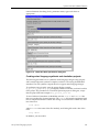
Figure 2-2: User-Defined Precision Options (available if selected instead of full
precision)
Valid and Invalid Data
In the Xilinx Blockset portion of a Simulink model, every data sample is accompanied
by a handshake validation signal. In the corresponding hardware, every data-carrying
bus has a companion net that carries a valid or invalid status indicator. This is a
commonly used handshaking mechanism. There are different circumstances under
which the status indicator may be set to invalid. For example, invalid data might
mean that a pipeline has not yet filled up, or it may denote bursty outputs, as with an
FFT. Blocks in the Xilinx Blockset can use this valid bit signal to determine what to do
with the input data. Some of the Xilinx blocks, for example, the storage blocks and the
FFT, use the valid bit to determine when to store input data.
Port Data Types
Selecting the Port Data Types option (under the Format menu in the Simulink
window) shows the data type and precision of a signal. An example port data type
string is Fix_11_9, which indicates that the signal is a signed 11-bit number with the
binary point 9 bits from the right side. Similarly, an unsigned signal is indicated by the
UFix_ prefix.
The Nature of Signals in the Xilinx Blockset
17
Xilinx System Generator v2.1 Reference Guide
Use of Xilinx Smart-IP Cores by the System Generator
To increase hardware performance, most System Generator blocks are implemented
using Xilinx Smart-IP (Intellectual Property) LogiCOREs. These are hand crafted
modules that make optimal use of FPGA resources to maximize performance. Some
System Generator blocks map onto multiple LogiCOREs, for example, the 1024-point
FFT, maps onto Dual Port Memory blocks as well as the FFT core itself.
Some Xilinx blocks also can be implemented as synthesizable VHDL modules, hence
the LogiCORE is an option. When such a block cannot be implemented as a
LogiCORE, System Generator automatically maps the block onto the synthesizable
module. For example, the Xilinx Negate block generates a LogiCORE if you specify
input of up to 256 bits, but for more than 256 bits the block is realized in synthesizable
VHDL.
Many Xilinx blocks have implementations only as LogiCOREs. The reason for this is
circuit performance. Because they are handcrafted for FPGA implementation,
LogiCOREs have predictable performance in all design contexts. For example, the
Xilinx FIR Filter block can be implemented only as the Distributed Arithmetic FIR
Filter LogiCORE.
During algorithm exploration in Simulink and System Generator, it is common to
iterate through block customization, Simulink simulation, and code generation. When
you incorporate Black Box functionality, you can also add HDL simulation to this
flow. To speed this design cycle, it is possible to instruct System Generator to not
invoke Xilinx CORE Generator to re-generate LogiCOREs that have already been
generated and have not changed. This can be done on individual blocks by the
Generate Core checkbox control, or globally using the System Generator block
parameters dialog box.
Licensed Cores
The System Generator targets a suite of new ready-to-use licensed LogiCORE
algorithms for forward error correction (FEC), which are critical for detecting and
correcting errors in wired and wireless communication systems during transmission
of data to optimize the use of available bandwidth. The new algorithms include ReedSolomon Encoder/ Decoder, a Viterbi Decoder, and an Interleaver/De-interleaver.
These cores may be used for communication applications such as broadcast
equipment, wireless LAN, cable modems, xDSL, satellite communications,
microwave networks, and digital TV.
The System Generator allows you to build and simulate your FEC designs in Simulink
using the Xilinx Blockset Communication library. System Generator creates a VHDL
design and testbench that allows you to do a VHDL simulation of the FEC cores. Free
evaluation versions of the FEC cores provide the behavioral models needed for VHDL
simulation. The System Generator will allow you to generate the licensed core using
the Xilinx CORE Generator after you have purchased and installed the FEC cores.
Licensing information, as well as instructions for downloading the cores, can be
found at the Xilinx IP Center:
http://www.xilinx.com/ipcenter/fec_index.htm.
18
Xilinx Development System
Xilinx Blockset Overview
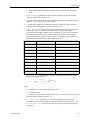
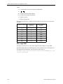
Xilinx LogiCORE Versions
The Xilinx LogiCORE blocks (indicating the version numbers being supported by
the System Generator) used in Xilinx System Generator v2.1 are listed below.
Xilinx Block
Xilinx LogiCORE
Version
Accumulator
ACCUMULATOR
V5.0
Addressable Shift
Register
RAM_SHIFT
V5.0
Adder/Subtractor
ADDSUB
V5.0
CIC
CIC
V1.0
Counter
BINARY_COUNTER
V5.0
Constant Multiplier
MULT_GEN
V4.0
Convolutional
Encoder
CONVOLUTION
V1.0
DDS
DDS
V4.0
Dual Port Ram
MEM_DP_BLOCK
V3.2
FIFO
SYNC_FIFO
V3.0
FFT
FFT and MEM_DP_BLOCK
V1.0 (Virtex, Spartan-II),
V2.0 (Virtex-II)
V3.2 (MEM_DP_BLOCK)
FIR Filter
DA_FIR
V6.0
Interleaver/
Deinterleaver
INTERLEAVER
V1.1
Inverter
GATE_BUS
V5.0
Logical
GATE_BUS
V5.0
Multiplier (mult)
MULT_GEN
V4.0
Mutiplexer (mux)
BUS_MUX
V5.0
Negate
TWOS_COMP
V5.0
Relational
COMPARE
V5.0
RS Decoder
RS_DECODER
V2.0
RS Encoder
RS_ENCODER
V2.0
Sine Cosine
SIN_COS
V3.0
Single Port RAM
MEM_SP_BLOCK and
DIST_MEM
V3.2(BRAM), V5.0 (dist.)
State Machines
MEM_SP_BLOCK and
DIST_MEM
V3.2(BRAM), V5.0 (dist.)
ROM
MEM_SP_BLOCK and
DIST_MEM
V3.2 (BRAM), V5.0 (dist.)
Viterbi Decoder
VITERBI
V1.0
Common Options in Block Parameters Dialog Box
Each Xilinx block has several configurable parameters, seen in the block parameters
dialog box. Many of these parameters are specific to that particular block. Those block
Common Options in Block Parameters Dialog Box
19
Xilinx System Generator v2.1 Reference Guide
specific parameters are described in the specific block documentation in the next
chapter.
The remainder of the parameters in each block’s parameters dialog box are common
to most blocks. These common parameters are described below.
Arithmetic Type
In the Type field of the block parameters dialog box, you can choose unsigned or
signed (two’s complement) as the datatype of the output signal.
Implement with Xilinx Smart-IP Core (if possible)
This checkbox (sometimes referred to as the Use Core checkbox) asks the software to
instantiate a core in the generated VHDL. If you do not select this checkbox, the
software will instead create synthesizable VHDL.
Selecting this option does not guarantee that a Xilinx LogiCORE will be used. If the
parameters for your block are such that a core cannot be generated, synthesizable
VHDL will be generated instead. The System Generator software determines this at
code generation time.
Generate Core
When the Generate Core checkbox is selected, the Xilinx CORE Generator will be
invoked during System Generator code generation. If Generate Core is not selected, a
Xilinx LogiCORE will not be generated, and if the core doesn’t already exist in your
project directory, subsequently running the Xilinx Implementation tools will produce
an error.
If you select Implement with Xilinx Smart-IP Core but do not select
Generate Core, you will be able to simulate your generated VHDL because (1) a
core will be instantiated in the VHDL, and (2) the behavioral VHDL models will be
available for a simulator to use. However, you will not be able to complete
implementation into a Xilinx FPGA until you have also generated the core.
In some blocks, only the Generate Core option is available. If the Implement
with Smart IP-Core option is not available, only a core implementation is
available from the System Generator, but no synthesizable VHDL implementation.
Use Placement Information for Core
If Generate Core is selected,the generated core includes relative placement
information. This generally results in a faster implementation. Because the placement
is constrained by this information, it can sometimes hinder the place and route
software.
Latency
Many elements in the Xilinx Blockset have a latency option. This defines the number
of sample periods by which the block’s output is delayed. One sample period may
correspond to multiple clock cycles in the corresponding FPGA implementation (for
example, when the hardware is overclocked with respect to the Simulink model).
System Generator v2.1 does not perform extensive pipelining; additional latency is
usually implemented as a shift register on the output of the block.
20
Xilinx Development System
Xilinx Blockset Overview
Precision
The fundamental computational mode in the Xilinx Blockset is arbitrary precision
fixed point arithmetic. Most blocks give you the option of choosing the precision, i.e.
the number of bits and binary point position.
By default, the output of Xilinx blocks is full precision; that is, sufficient precision to
represent the result without error. Most blocks have a User-Defined precision option
that fixes the number of total and fractional bits.
Number of Bits
When you have specify user-defined precision, you will be asked to specify how
many bits the output should have.
Binary Point
You will also be asked to specify how many bits are to the right of the binary point
(i.e., the size of the fraction). The binary point position must be between zero and the
number of bits in the number’s container.
Overflow and Quantization
When user-defined precision is selected, errors may result from overflow or
quantization. Overflow occurs if a value lies outside the representable range.
Quantization error occurs if the number of fractional bits is insufficient to represent
the fractional portion of a value.
The Xilinx fixed point data type supports several options for user-defined precision.
In the case of overflow, the options are to saturate to the largest positive (or smallest
negative) value, wrap the value (i.e., discard any significant bits beyond the mostsignificant bit in the fixed point number), or flag an overflow as a Simulink error
during simulation.
In the case of quantization, the options are to round to the nearest representable value
or to the value farthest from zero if there are two equidistant nearest representable
values, or to truncate the data (i.e., discard bits to the right of the least significant bit).
It is important to realize that whatever option is selected, the generated HDL model
and Simulink model will behave identically.
Override with Doubles
An Override with Doubles message appears on many Xilinx Blocks, with some
variations. Variations are:
Override Computation with Doubles
Override Constant with Double
Override Output with Doubles
Override Storage with Doubles
Most Simulink blocks use double precision floating point signals and arithmetic.
However, when such a signal passes through Xilinx Gateway In block, it is converted
to a fixed point signal. Later, when passing through a Xilinx Gateway Out block, the
signals are converted back into double precision floating point.
Common Options in Block Parameters Dialog Box
21
Xilinx System Generator v2.1 Reference Guide
In the Simulink environment, the Override with Doubles option allows you to
simulate the entire design in double precision floating point.
This option is useful in selecting fixed point widths or when debugging. If you detect
unacceptable quahtization errors with fixed point signals, you can choose to simulate
your entire design, or only specific blocks, using double precision floating point
signals and arithmetic operations. This option will help you discover which part of
your design is responsible for the unacceptable quantization error.
You may choose Override with Doubles on a particular block. You may also choose
this option for an entire sheet or an entire subsystem (the sheet plus underlying
hierarchy) by instantiating a System Generator token on the sheet, and choosing
Override with Doubles as one of the System Generator block’s configurable
parameters.
When the output of one block with Override with Doubles set is connected to the
input of another block where the option is also set, data samples are transmitted in
double precision.
You can easily identify which blocks are currently set to Override with Doubles.
When this option is set, affected Xilinx blocks are displayed in gray rather than the
normal blue or yellow.
Sample Period
Data streams are processed at a specific sample rate as they flow through Simulink.
Typically, each block detects the input sample rate and produces the correct sample
rate on its output. Xilinx blocks Up Sample and Down Sample provide a means to
increase or decrease sample rates.
Use Explicit Sample Period
If you select Use Explicit Sample Period rather than the default, you may set the
sample period required for all the block outputs. This is useful when implementing
features such as feedback loops in your design. In a feedback loop, it is not possible
for the System Generator to determine a default sample rate, because the loop makes
an input sample rate depend on a yet-to-be-determined output sample rate. System
Generator under these circumstances requires you to supply a hint to establish sample
periods throughout a loop.
The following image (the Concat block’s parameters dialog box) shows the options
with Use Explicit Sample Period selected.
Figure 2-3: Use Explicit Sample Period options (available if selected)
22
Xilinx Development System
Xilinx Blocks
Chapter 3
Xilinx Blocks
This chapter describes each Xilinx block in detail. Xilinx blocks are grouped within six
categories, also shown in the Simulink library browser. They are:
•
Basic Elements
•
Communication
•
DSP
•
Math
•
MATLAB I/O
•
Memory
•
State Machine
Basic Elements
The Xilinx Basic Elements library includes the standard building blocks for digital
designs. Using these blocks, you may insert delay, change the sample rate, and
introduce constants, counters, multiplexers, etc. The Basic Elements library also has
two special blocks: the System Generator and the Black Box.
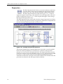
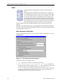
System Generator
The System Generator is a special Xilinx block that invokes the tool’s
code generation software.
By placing the System Generator token on your Simulink project sheet,
you can generate HDL and Xilinx LogiCOREs for all the Xilinx blocks
on that sheet and on any sheets beneath it in the hierarchy. The System
Generator block parameters dialog box allows you to tailor your
Simulink simulation and code generation.
Basic Elements
23
Xilinx System Generator v2.1 Reference Guide
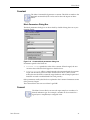
Block Parameters Dialog Box
The block parameters dialog box can be invoked by double-clicking the icon in your
Simulink model.
Figure 3-1: System Generator block parameters dialog box
Parameters specific to the System Generator block are:
•
Xilinx Product Family
Supported families currently are: Virtex, Virtex2, Spartan2, and VirtexE.
•
Target Directory
Specify where the output files (VHDL, cores, and project files) will be written. It is
suggested that you create a separate directory (away from your Simulink model
files) to generate your files in order to keep your Xilinx project files and Simulink
model files directories organized separately.
•
System Clock Period
Enter the desired System Clock Period of your design in nanoseconds (ns). This
information will be passed to the Xilinx software tools through the user
constraints file (.ucf) that will be created by the System Generator. This value
will be used as the global PERIOD constraint and multi-cycle paths will be
constrained to a multiple of this value.
•
Create Testbench
Checking the Create Testbench box instructs the tool to save test vectors to be
used downstream, during behavioral simulation.
When the Create Testbench box is checked, a VHDL testbench wrapper file is
created for your design. Data vectors (created during Simulink simulation) are
also generated.
24
Xilinx Development System
Xilinx Blocks
The wrapper file is named to match the top level VHDL file generated for your
project. For example, if your top level file is named design_project, the
wrapper is called design_project_testbench.vhd. The top level of the
project is taken to be the Simulink sheet from which you invoked the System
Generator token.
In addition to the testbench VHDL file, test vectors (.dat files) are also generated.
These vectors represent the inputs and expected outputs seen in Simulink
simulation. The testbench (which uses these test vectors) can be run in a
behavioral simulator such as ModelSim from Model Technology. It will report any
discrepancies between the Simulink and VHDL simulations.
•
Global Clock Enable and Global Clear
A global clock enable or clear clock signal can be added to the design by selecting
these options. This may result in a large fanout signal thus degrading system
performance. Use this option only if absolutely necessary.
•
Override with Doubles
The System Generator token allows you to override fixed point values with
double precision values for your Simulink simulation. This is particularly useful
during design and debugging. The Override with Doubles directive from a
System Generator token is applied to all Xilinx blocks on the same sheet and
recursively through all subsystems on the sheet. Additional System Generator
tokens can be inserted into the subsystems to selectively mask this effect. For an
explanation of the Override with Doubles behavior, see the Common
Parameters section of the previous chapter.
•
Generate Cores
The Generate Cores pulldown menu on the System Generator token gives three
ways to determine for which blocks the Xilinx LogiCOREs should be generated. They
are:
•
♦
According to Block Masks: Each block that uses a Xilinx LogiCORE has
a Generate Core checkbox on its parameters dialog box. When
According to Block Masks is selected on the System Generator dialog,
a core is generated for each block whose Generate Core box is checked.
♦
Everywhere Available: When Everywhere Available is selected,
cores are generated without regard to the settings of Generate Core checkboxes on individual blocks.
♦
Not Needed - Already Generated: When Not Needed - Already
Generated is selected, no cores are generated. This is useful in the early
stages of design development because it saves the time that would otherwise
be used in unnecessary calls to the Xilinx CORE Generator. When, in the later
stages, you plan to run the design through the Xilinx Implementation tools,
you must remember to regenerate your design with According to Block
Masks or Everywhere Available selected so that your cores are up to
date.
Generate button
Finally, clicking the Generate button invokes the code generation software, and
your Simulink design is converted to VHDL and Xilinx LogiCOREs. Note that the
Cancel button is active during code generation. If you want to cancel the code
generation phase while it is running, you may do so by selecting Cancel during
code generation.
Basic Elements
25
Xilinx System Generator v2.1 Reference Guide
Addressable Shift Register
The Xilinx Addressable Shift Register block is a variable-length
shift register (or delay chain). This block differs from the Xilinx
Delay block in that the amount of latency experienced by data
from input to block output is variable and depends on the address
value.
Data presented to the block will traverse the entire delay chain.
The output of the block is not necessarily the output of the last register in the chain,
however. Instead, the output of the block is taken from the register pointed to by the
address presented on the addr port.
Block Interface
The block interface (inputs and outputs as seen on the Addressable Shift Register
icon) are as follows:
Input signals:
d
data input
addr
address
en
enable signal
Output signals:
q
data output
In Simulink, the addr port is given priority over the data (d) port, i.e. on each
successive cycle, the addressed data value is read from the register before the shift
operation occurs. This order is needed in the Simulink software model to guarantee
one clock cycle of latency between the data port and the first register of the delay
chain. (If the shift operation were to come first, followed by the read, then there would
be no delay, and the hardware would be incorrect.)
26
Xilinx Development System
Xilinx Blocks
Block Parameters Dialog Box
The Addressable Shift Register Block Parameters Dialog Box can be invoked by
double-clicking the icon in your Simulink model.
Figure 3-2: Addressable Shift Register block parameters dialog box
Parameters specific to the Addressable Shift Register block are:
•
Infer Maximum Latency (depth) using Address Port Width: you can
choose to allow the block to automatically determine the depth or maximum
latency of the shift-register based on the bit-width of the address port.
•
Maximum Latency (depth): In the case thaqt the maximum latency is not
inferred (previous option), the maximum latency can be set explicitly. It must be a
positive integer.
•
Allow Additional Hardware in Certain Rate-Change Cases: several
rate-change conditions require the use of extra hardware beyond that used by the
IP core to make it compliant with the Simulink simulation output. A rate-change
condition will be detected if the address and data rates differ and the address port
is running at a non-system rate. Choosing this parameter allows additonal
hardware to be used in these cases.
•
Use Enable Port: when checked, the optional enable port is activated.
Other parameters used by this block are explained in the Common Parameters section
of the previous chapter.
Xilinx LogiCORE
The block always uses the Xilinx LogiCORE Ram-based Shift Register V5.0. When the
Generate Core parameter is checked, the Use Placement Information
parameter provides the option of generating the core as a Relationally Placed Macro
(RPM) or as unplaced logic.
The core datasheet can be found on your local disk at:
%XILINX%\coregen\ip\xilinx\eip1\com\xilinx\ip\baseblox_v5_0\do
c\ram_shift.pdf
Basic Elements
27
Xilinx System Generator v2.1 Reference Guide
Black Box
The Xilinx Black Box token enables you to instantiate your own
specialized functions in your model, and subsequently into a generated
design. Like the System Generator token, the Black Box token can be
placed in any Simulink subsystem, identifying the subsystem as a black
box. If you choose to include functionality in your Simulink model that
does not exist in the current blockset, any Simulink subsystem can be
treated as a black box. You may want to build a model out of non-Xilinx blocks for an
HDL representation of functionality that you want to turn into a Simulink model.
To create a black box in the System Generator, you must supply both a Simulink
model and a corresponding HDL file.
Incorporating mixed language black boxes
System Generator creates VHDL for the Xilinx blocks in your design. But if you
include a black box that is written in Verilog HDL, System Generator will produce a
mixed language project.
A VHDL black box and a Verilog black box share the same interface, as is seen below
in the description of the block parameters. You must specify the VHDL/Verilog
design unit name, and specify types, names, and values of generics or parameters.
You must also specify how many clocks the black box has and how these clocks
should be associated with ports.
In addition, you must specify whether you are inserting a VHDL black box or a
Verilog black box by choosing the appropriate language in the HDL Language option
on the Black Box block parameter dialog. System Generator will generate a
corresponding wrapper in the chosen language.
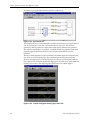
Block Parameters Dialog Box
The Black Box block parameters dialog box encapsulates the design information
necessary for the compiler to create the correct instantiation interfaces. This black box
support allows you to abstract commonly used control signals and ports, and then
28
Xilinx Development System
Xilinx Blocks
infer them in the generated VHDL. The block parameters dialog box can be invoked
by double-clicking the icon in your Simulink model.
Figure 3-3: Black Box block parameters dialog box
Parameters specified as cell arrays (generic or parameter names, types, and values)
permit several methods for entering data. You can specify your data directly in the
dialog box as shown. You may also specify the cell arrays as MATLAB expressions.
This is useful if you have many elements in your cell arrays. Generic types can be any
VHDL type. Parameter types can be any Verilog type.
The black box block parameters dialog box allows you to specify multiple clocks on a
black box. To handle more than one clock, the System Generator must be told how fast
each clock should run. To specify a clock’s speed, you must associate the clock to a
port on the black box; the frequency of the clock is then the frequency of the signal
passing through the port. System Generator allows more than one port to be
associated to a clock, but all associated ports must have the same frequency.
Note - Constant inputs match any paired frequency.
For example, a black box with two ports (a fast input and a slow output) should have
clocks called fast_clk and slow_clk with frequencies that match those of the
Basic Elements
29
Xilinx System Generator v2.1 Reference Guide
input and output ports respectively. To configure the black box, enter the parameters
in the black box block parameters dialog box as shown in the figure below.
Figure 3-4: Customizing Clocks in the Black Box block parameters dialog box
These settings indicate that the black box should have clocks named fast_clk and
slow_clk. The fast_clk should have the same frequency as the samples presented
to input port #1, and the slow_clk should have the same frequency as output port
#1.
Concat
The Xilinx Concat block performs a concatenation of two bit vectors
represented by unsigned integer numbers, i.e. two unsigned numbers
with binary points at position zero.
The Xilinx Reinterpret block provides capabilities that can extend the
functionality of the Concat block.
Block Interface
The block has two input ports and one output port. The two input ports are labeled
hi and low. The number input to the hi port will occupy the most significant bits of
the output and the number that is input to the low port will occupy the least
significant bits of the output.
Block Parameters Dialog Box
The block parameters dialog box can be invoked by double-clicking the icon in your
Simulink model.
Figure 3-5: Concat block parameters dialog box
Parameters used by this block are explained in the Common Parameters section of the
previous chapter.
The Concat block does not use a Xilinx LogiCORE.
30
Xilinx Development System
Xilinx Blocks
Constant
The Xilinx Constant block generates a constant. This block is similar to the
Simulink constant block, but can be used to drive the inputs on Xilinx
blocks.
Block Parameters Dialog Box
The block parameters dialog box can be invoked by double-clicking the icon in your
Simulink model.
Figure 3-6: Constant block parameters dialog box
Parameters specific to the block are:
•
Constant Value: specifies the value of the constant. When changed, the new
constant value of the block will appear on the block icon.
•
Sampled Constant: allows a sample period to be associated with the constant
ouput and inherited by blocks that the constant block drives. (This is useful
mainly because the blocks eventually target hardware and the sample periods of
Simulink are used to establish hardware clock periods.)
Other parameters used by this block are explained in the Common Parameters section
of the previous chapter.
The Constant block does not use a Xilinx LogiCORE.
Convert
The Xilinx Convert block converts each input sample to a number of a
desired arithmetic type. For example, a number can be converted to a
signed (two’s complement) or unsigned value.
Basic Elements
31
Xilinx System Generator v2.1 Reference Guide
Block Parameters Dialog Box
The block parameters dialog box can be invoked by double-clicking the icon in your
Simulink model.
Figure 3-7: Convert block parameters dialog box
All the parameters of the Convert block are parameters common to other blocks.
Please refer to the Common Parameters section in the previous chapter for details.
Parameters defining the desired output type are:
•
Output Arithmetic Type
•
Number of Bits
•
Binary Point
Parameters defining the quantization effect and the overflow effect are:
•
Quantization Behavior
•
Overflow Behavior
The Convert block does not use a Xilinx LogiCORE.
Counter
The Xilinx Counter block implements an up or down counter. It can be
configured to step between the starting and ending values, provided the
increment evenly divides the difference between the starting and ending
values. The counter output and increment values can be fixed point
numbers in addition to integers.
The output for an up counter is calculated as follows:
The down counter calculation replaces addition by subtraction.
32
Xilinx Development System
Xilinx Blocks
The block can be configured as a free running up or down counter by
selecting the Provide Reset Pin option on the block parameters
dialog box. In this case, the block has a reset input port in addition to its
output port.
The output for a free running up counter is calculated as follows:
Here N denotes the number of bits in the counter. The down counter calculations
replace addition by subtraction.
The free running up or down counter can be configured to load the
output of the counter with a value on the input din port by selecting the
Provide Load Pin option on the block parameters dialog box.
In this case, the block has three (rst, Load, din) input ports in
addition to its output port.
The output for a free running up counter with load capability is calculated as follows:
Here N denotes the number of bits in the counter. The down counter calculations
replace addition by subtraction.
Basic Elements
33
Xilinx System Generator v2.1 Reference Guide
Block Parameters Dialog Box
The Counter block parameters dialog box is invoked by double-clicking the block
icon.
Figure 3-8: Counter block parameters dialog box
Parameters specific to the block are:
•
Number of Bits: specifies the number of bits in the counter.
•
Binary Point Position: specifies the location of the binary point.
•
Arithmetic Type: specifies the block ouput to be either Signed or Unsigned.
•
Start Count at: specifies the starting and reset value. The default is zero.
•
Count to Value: specifies the ending value, the number at which the counter
resets. A value of Inf denotes the largest representable output in the specified
precision. This cannot be the same as the start count.
•
Count By Value: specifies the increment, which must evenly divide the
difference between the extreme values.
•
Count Direction: specifies the direction of the count (Up or Down).
•
Provide Reset Pin: when checked, the block operates as a free running
counter with explicit reset port. In this case, there is no Count to Value setting.
•
Provide Load Pin: when checked, the block operates as a free running load
counter with explicit load and din port. The load capability is available only for
free running counter.
Other parameters used by this block are described in the Common Parameters section
of the previous chapter.
34
Xilinx Development System
Xilinx Blocks
Xilinx LogiCORE
The block always uses the Xilinx LogiCORE: Binary Counter V5.0.
The Core datasheet can be found on your local disk at:
%XILINX%\coregen\ip\xilinx\eip1\com\xilinx\ip\baseblox_v5_0\do
c\binary_counter.pdf
Delay
The Xilinx Delay block is a delay line (also called a shift register) of
configurable length, allowing you to add latency to your design. Data
presented at the input will appear at the output after a user specified
number of sample periods.
The Delay block differs from the Register in that the Register allows only
latency of 1, and contains an Initial Value parameter. The Delay block supports a user
specified latency, but no initial value, other than zeroes.
Block Parameters Dialog Box
The block parameters dialog box can be invoked by double-clicking the icon in your
Simulink model.
Figure 3-9: Delay block parameters dialog box
Parameters specific to this block are:
•
Initialize with Zeros: The block’s internal registers are set to zero if this
option is selected, otherwise the output will be NaN (Not a Number) until the
registers are flushed. For example, if the Delay block has a latency of 5 and this
option is selected, the first five output values will be zeros. If this option is not
selected, the first five output values will be NaN.
•
Latency: You may set the amount of latency in the Latency field.
Other parameters used by this block are explained in the Common Parameters section
of the previous chapter.
The Delay block does not use a Xilinx LogiCORE, but is efficiently mapped to utilize
the SRL16 feature of Xilinx devices.
Basic Elements
35
Xilinx System Generator v2.1 Reference Guide
Down Sample
The Xilinx Down Sample block reduces the sample rate at the point
where the block is placed in your design. The input signal is undersampled so that every nth input sample is presented at the output and
held.
Output sample period is ki, where k is the sampling rate and i is
the input sample period.
In Simulink, a block changes its output right after it is enabled. In hardware, a
register does not change until the clock enable is sampled, i.e. one clock cycle later. To
make the hardware cycle-true to the Simulink model, the down sample block is
implemented with the following circuit in hardware:
Figure 3-10: Hardware implementation of down sample block
The clock enable connected to this circuit is the same one that is distributed to the
blocks connected to its output. The timing diagram shown below demonstrates the
circuit's behavior. It is important to notice that this circuit has a combinatorial path
from din to dout. Whenever possible put a register or delay block after a down
sample block.
Figure 3-11: Down sample circuit behavior
36
Xilinx Development System
Xilinx Blocks
Block Parameters Dialog Box
The block parameters dialog box can be invoked by double-clicking the icon in your
Simulink model.
Figure 3-12: Down sample block parameters dialog box
Parameters specific to the block are:
•
Sampling Rate: must be an integer greater or equal to 2. This is the ratio of the
output sample period to the input, and is essentially a sample rate divider. For
example, a ratio of 2 indicates a 2:1 division of the input sample rate. If a noninteger ratio is desired, the Up Sample block can be used in combination with the
Down Sample block.
•
Zero Initial Output (otherwise NaN): NaN means Not a Number. This
option lets you choose what the first value of the new sample (before it has valid
data) will be. By selecting Zero Initial Output, you can validate the first sample
with valid data of zero. Otherwise, an invalid data (NaN) will be the block’s first
output.
Other parameters used by this block are explained in the Common Parameters section
of the previous chapter.
The Down Sample block does not use a Xilinx LogiCORE.
Get Valid Bit
The Xilinx Get Valid Bit element sets its output to 1 when its input is a
valid data value. The output is set to 0 otherwise.
In the Xilinx Blockset, every data sample that flows through the model is
accompanied by a handshake validation signal. In the corresponding
hardware, every data-carrying bus has a companion net that carries a
status indicator. Under different circumstances the status indicator may be set to
invalid. For example, a pipeline might not yet have filled, or outputs might be bursty,
as with an FFT. This block simply reports the valid status of the samples presented to
it.
There are no parameters for this block.
Basic Elements
37
Xilinx System Generator v2.1 Reference Guide
Mux
The Xilinx Mux block implements a multiplexer.
The block has one select input (type unsigned) and a userconfigurable number of data bus inputs, ranging from 2 to
32.
Block Parameters Dialog Box
The block parameters dialog box can be invoked by double-clicking the icon in your
Simulink model.
Figure 3-13: Mux block parameters dialog box
Parameters specific to the block are:
•
Number of Inputs: specifies the number of data bus inputs, from 2 to 32.
•
Use Placement Information for Core: when checked, the generated core
includes relative placement information. This usually results in a faster
implementation. The resulting floorplan is a single column with two bits per slice.
With this placement, large multiplexers may not fit into small Xilinx devices.
When unchecked, the core is generated as unplaced logic.
Other parameters used by this block are described in the Common Parameters section
of the previous chapter.
Xilinx LogiCORE
The block uses the Xilinx LogiCORE Bus Multiplexer V5.0. When the Generate Core
parameter is checked, the Use Placement Information for Core parameter provides the
option of generating the core as a Relationally Placed Macro (RPM) or as unplaced
logic.
The Core datasheet can be found on your local disk at:
38
Xilinx Development System
Xilinx Blocks
%XILINX%\coregen\ip\xilinx\eip1\com\xilinx\ip\baseblox_v5_0\do
c\bus_mux.pdf
Parallel to Serial
The Parallel to Serial block takes an input word and splits it into N time
multiplexed output words where N equals the number of input bits/
number of output bits. The order of the output is either least significant
bit first or most significant bit first.
The following waveform illustrates the block’s behavior:
Figure 3-14: Example of Parallel to Serial behavior
This example illustrates the case where the input width is 4, output width is 2, word
size is 1 bit, and the block is configured to output the least significant partial word
first.
Block Interface
The Parallel to Serial block has one input and one output port. The input port can be
any size. The output port size is indicated on the block parameters dialog box.
Basic Elements
39
Xilinx System Generator v2.1 Reference Guide
Block Parameters Dialog Box
Figure 3-15: Parallel to Serial block parameters dialog box
Parameters specific to the block are:
•
Output Order: Most significant word first or least significant word first. Word
size is determined by the size of the input port.
•
Output Arithmetic Type: unsigned or signed
•
Number of Input Bits: Input width. Must match size of input port.
•
Number of Output Bits: Output width. Must divide Number of Input
Bits evenly.
•
Binary Point: Output binary point location.
An error is reported when the number of output bits does not evenly divide the
number of input bits.
The minimum latency of this block is 1.
Other parameters used by this block are explained in the Common Parameters section
of the previous chapter.
The Parallel to Serial block does not use a Xilinx LogiCORE.
Register
The Xilinx Register block models a D flip flop-based register, having
latency of one sample period.
40
Xilinx Development System
Xilinx Blocks
Block Interface
The block has one input port for the data and an optional input reset port. The initial
output value is specified by the user in the block parameters dialog box (below). Data
presented at the input will appear at the output after one sample period. Upon reset,
the register assumes the initial value specified in the parameters dialog box.
The Register block differs from the Xilinx Delay block by providing an optional reset
port and a user specifiable initial value.
Block Parameters Dialog Box
The block parameters dialog box can be invoked by double-clicking the icon in your
Simulink model.
Figure 3-16: Register block parameters dialog box
Parameters specific to the block are:
•
Initial Value: specifies the initial value in the register.
•
Quantization (of Initital Value): specifies desired quantization effect;
one on Round or Truncate.
•
Overflow Effect (of Initital Value): specifies desired overflow effect;
Wrap, Saturate, or Flag as Error.
•
Register Only Valid Data: when checked, only valid values are registered.
Extra logic is added when this option is selected, thus decreasing system
performance.
•
Use Reset Port: when checked, the optional reset port is activated.
•
Use Enable Port: when checked, the optional clock enable port is activated.
Other parameters used by this block are explained in the Common Parameters section
of the previous chapter.
The Register block is implemented as a synthesizable VHDL module. It does not use a
Xilinx LogiCORE.
Basic Elements
41
Xilinx System Generator v2.1 Reference Guide
Reinterpret
The Reinterpret block forces its output to a new type without any
regard for retaining the numerical value represented by the input. The
binary representation is passed through unchanged, so in hardware this
block consumes no resources. The number of bits in the output will
always be the same as the number of bits in the input.
The block allows for unsigned data to be reinterpreted as signed data, or, conversely,
for signed data to be reinterpreted as unsigned. It also allows for the reinterpretation
of the data’s scaling, through the repositioning of the binary point within the data.
The Xilinx Scale block provides an analagous capability.
An example of this block’s use is as follows: if the input type is 6 bits wide and signed,
with 2 fractional bits and the output type is forced to be unsigned with 0 fractional
bits, then an input of -2.0 (1110.00 in binary, two’s complement) would be translated
into an output of 56 (111000 in binary).
This block can be particularly useful in applications that combine it with the Xilinx
Slice block or the Xilinx Concat block. To illustrate the block’s use, consider the
following scenario:
Given two signals, one carrying signed data and the other carrying two unsigned
bits (a UFix_2_0), we want to design a system that concatenates the two bits
from the second signal onto the tail (least significant bits) of the signed signal.
We can do so using two Reinterpret blocks and one Concat block. The first
Reinterpret block is used to force the signed input signal to be treated as an
unsigned value with its binary point at zero. The result is then fed through the
Concat block along with the other signal’s UFix_2_0. The Concat operation is
then followed by a second Reinterpret that forces the output of the Concat block
back into a signed interpretation with the binary point appropriately
repositioned.
Though three blocks are required in this construction, the hardware
implementation will be realized as simply a bus concatenation, which has no cost
in hardware.
42
Xilinx Development System
Xilinx Blocks
Block Parameters Dialog box
Figure 3-17: Reinterpret block parameters dialog box
Parameters specific to the block are:
•
Force Arithmetic Type: When checked, the Output Arithmetic Type
parameter can be set and the output type will be forced to the arithmetic type
chosen according to the setting of the Output Arithmetic Type parameter. When
unchecked, the arithmetic type of the output will be unchanged from the
arithmetic type of the input.
•
Force Binary Point Position: When checked, the Output Binary Point
parameter can be set and the binary point position of the output will be forced to
the position supplied in the Output Binary Point parameter. When unchecked, the
arithmetic type of the output will be unchanged from the arithmetic type of the
input.
•
Output Arithmetic Type: The arithemetic type (unsigned or signed, 2’s
complement) to which the output is to be forced.
•
Output Binary Point: The position to which the output’s binary point is to be
forced. The supplied value must be an integer between zero and the number of
bits in the input (inclusive).
This block does not use any hardware resources. The block does not use a Xilinx
LogiCORE.
Serial to Parallel
The Serial to Parallel block takes a series of inputs of any size and
creates a single output of a specified multiple of that size. The input
series can be ordered either with the most significant word first or the
least significant word first.
Basic Elements
43
Xilinx System Generator v2.1 Reference Guide
The following waveform illustrates the block’s behavior:
Figure 3-18: Example of Serial to Parallel behavior
This example illustrates the case where the input width is 1, output width is 4, word
size is 1 bit, and the block is configured for most significant word first.
Block Interface
The Serial to Parallel block has one input and one output port. The input port can be
any size. The output port size is indicated on the block parameters dialog box.
Block Parameters Dialog Box
Figure 3-19: Serial to Parallel block parameters dialog box
Parameters specific to the block are:
44
•
Input Order: Most Significant Word First or Least Significant Word First
•
Output Arithmetic Type: Unsigned or Signed
•
Number of Input Bits: Input width. Must match size of input port.
•
Number of Output Bits: Output width which must be a multiple of the
number of input bits.
Xilinx Development System
Xilinx Blocks
•
Binary Point: Output binary point location
Other parameters used by this block are explained in the Common Parameters section
of the previous chapter.
The Parallel to Serial block does not use a Xilinx LogiCORE.
An error is reported when the number of output bits cannot be divided evenly by the
number of input bits. The minimum latency for this block is zero.
Set Valid Bit
The Xilinx Set Valid Bit block flags input data as invalid when the signal
on the valid bit input port is zero. This block only sets data invalid; it
cannot change input data to valid.
In the Xilinx Blockset, every data sample that flows through the model
is accompanied by a handshake validation signal. In the corresponding
hardware, every data-carrying bus has a companion net that carries a valid or invalid
status indicator. This block provides some explicit control over this handshake
mechanism.
Block Parameters Dialog Box
The block parameters dialog box can be invoked by double-clicking the icon in your
Simulink model.
Figure 3-20: Set Valid Bit block parameters dialog box
Slice
The Xilinx Slice block allows you to slice off a sequence of bits from your
input data and create a new data value. This value is presented as the
output from the block. The output data type is unsigned with its binary
point at zero.
The block provides several mechanisms by which the sequence of bits
can be specified. If the input type is known at the time of parameterization, the
various mechanisms do not offer any gain in functionality. If, however, a Slice block is
used in a design where the input data width or binary point position are subject to
change, the variety of mechanisms becomes useful. The block can be configured, for
example, always to extract only the top bit of the input, or only the integral bits, or
Basic Elements
45
Xilinx System Generator v2.1 Reference Guide
only the first three fractional bits. The following diagram illustrates how to extract all
but the top 16 and bottom 8 bits of the input.
Figure 3-21: Slice block operation
Block Parameters Dialog Box
The block parameters dialog box can be invoked by double-clicking the icon in your
Simulink model.
46
Xilinx Development System
Xilinx Blocks
Figure 3-22: Slice block parameters dialog box showing different options
Parameters specific to the block are:
•
Specify Range As: (Two Bit Locations | Upper Bit Location + Width |Lower
Bit Location + Width). Allows the user to specify either the bit locations of both
end-points of the slice or one end-point along with number of bits to be taken in
the slice.
•
Width of Slice (Number of Bits): specifies the number of bits to extract.
•
Top bit of slice Offset by: specifies the offset for the ending bit position
from the LSB, MSB or binary point.
•
Bottom bit of slice Offset by: specifies the offset for the ending bit
position from the LSB, MSB or binary point.
•
Relative To: specifies the bit slice position relative to the Most Significant Bit
(MSB), Least Significant Bit (LSB), or Binary point of the top or the bottom of the
slice. Other parameters used by this block are explained in the Common
Parameters section of the previous chapter.
The Slice block does not use a Xilinx LogiCORE.
Sync
The Xilinx Sync Block synchronizes two to four channels of data so that
their first valid data samples appear aligned in time with the outputs.
The input of each channel is passed through a delay line and then
presented at the output port for that channel. The lengths of the delay
lines embedded in this block, however, are adaptively chosen at the
start of simulation so that the first valid input samples are aligned.
Thus, no data appears on any channel until a first valid sample has been received into
each channel.
Basic Elements
47
Xilinx System Generator v2.1 Reference Guide
The following diagram illustrates the operation of this block.
Figure 3-23: Sync block use
This diagram shows a two-channel Xilinx Sync Block connected to two signal sources,
with one producing a sawtooth wave and the other a sine wave. The sawtooth
generator is able to produce its output much more quickly than the sine generator.
This scenario could reflect, for example, a CORDIC-based sine generator with many
pipeline stages for hardware efficiency and a simple counter-based sawtooth
generator.
The rest of the diagram shows the connections of both the inputs and outputs of the
Sync block to a four-channel scope. The waveforms presented by that scope are
shown in the figure below. Note that the input waveforms are not aligned, with the
first valid sine wave samples significantly lagging the sawtooth wave. In the third and
fourth scope windows, the output signals can be seen to have been aligned.
Figure 3-24: Output of diagram showing Sync block use
48
Xilinx Development System
Xilinx Blocks
It is instructive to note that the following model produces behavior identical to the
one with the Sync block. This one, though, requires the designer to examine the two
upstream pipelined sources and to insert the correct delay line length to balance the
two pipelines. Moreover, should a pipeline stage be either added to or removed from
the sine wave generator, the pipeline balancing delay line would have to be re-tuned.
The Xilinx Sync block allows such balancing operations to be automated.
Figure 3-25: Design with delay rather than Sync block
The Sync block can be configured to have up to four channels and to add latency to all
channels beyond the minimum required.
Block Parameters Dialog Box
The block parameters dialog box can be invoked by double-clicking on the block icon
in your Simulink model. The dialog box is illustrated below.
Figure 3-26: Sync block parameters dialog box
Parameters specific to the block are:
Basic Elements
•
Number of channels: Specifies the number of channels to process, hence the
number of input and output ports. The number of channels can be 2, 3, or 4.
•
Latency (minimum per channel): Specifies the smallest amount of delay
that will be added to any channel. Latency will also be the amount of latency
49
Xilinx System Generator v2.1 Reference Guide
added to the channel that is last to present a valid input sample. Note that if this
parameter is zero, the block has a feed-through path; otherwise, it does not.
Other parameters used by this block are described in the Common Parameters section
of a previous chapter in this manual.
The Xilinx Sync block does not use a Xilinx LogiCORE.
Up Sample
The Xilinx Up Sample block increases the sample rate at the point
where the block is placed in your design. The input signal is oversampled so that every nth input sample is presented at the output, or
presented once with (n-1) zeroes interspersed.
The output sample period is i/k, where i is the input sample period
and k the sampling rate.
In Simulink, a block changes its output right after it is enabled. In hardware, a
register does not change until the clock enable is sampled, i.e. one clock cycle later. To
make the hardware cycle-true to the Simulink model, the up sample block is
implemented with the circuit shown below. The portion of the circuit within the
dashed line is always present. The additional mux used for zero padding is removed
if the Copy Samples option is selected on the block parameters dialog box.
Figure 3-27: Up sample block hardware implementation
The clock enable connected to this circuit is the same one that is distributed to the
blocks connected to its input. The timing diagram shown below demonstrates the
circuit's behavior. It is important to notice that this circuit has a combinatorial path
50
Xilinx Development System
Xilinx Blocks
from din to dout. Whenever possible, put a register or delay block after an up sample
block.
Figure 3-28: Example of up sample block behavior with zero padding
Block Parameters Dialog Box
The block parameters dialog box can be invoked by double-clicking the icon in your
Simulink model.
Figure 3-29: Up Sample block parameters dialog box
Parameters specific to the block are:
•
Sampling Rate: must be an integer with a value of 2 or greater. This is the ratio
of the output sample period to the input, and is essentially a sample rate
multiplier. For example, a ratio of 2 indicates a doubling of the input sample rate.
If a non-integer ratio is desired, the Up Sample block can be used in combination
with the Down Sample block.
•
Copy Samples: allows you to choose what to do with the additional samples
produced by the increased clock rate. By selecting Copy Samples, the same
sample will be duplicated (copied) during the extra sample times. If this checkbox
is not selected, the additional samples are zero.
Other parameters used by this block are explained in the Common Parameters section
of the previous chapter.
The Up Sample block does not use a Xilinx LogiCORE.
Basic Elements
51
Xilinx System Generator v2.1 Reference Guide
Communication
The blocks in the Communication library implement functions used in digital
communications systems, including convolutional and block channel coding,
interleaving, and utility functions.
Convolutional Encoder
The Xilinx Convolutional Encoder block implements an encoder
for convolutional codes. Commonly used in tandem with a
Viterbi decoder block, this block can be used to implement
forward error correction (FEC) circuitry for digital
communication systems.
Data is encoded using a linear feed forward shift register to
compute modulo-two sums over a sliding window of input
data, as shown in the figure below. The length of the shift register, and the code's
constraint length, is equal to the length of the convolution codes that characterize the
encoder, specified in the block’s parameters dialog box. These convolution codes
specify which bits in the data window contribute to the modulo-two sum at the
encoder output. Resetting the block will clear the contents of the shift register to all
zeros. The encoder rate is the ratio of input bits to output bits, so a rate 1/2 encoder
outputs two bits for each input bit. Similarly, a rate 1/3 encoder outputs three bits for
each input bit.
Figure 3-30: Constraint length 9 convolutional encoder
Block Interface
The block has two input and one output ports. The input ports, din and rst, are
limited to type UFix1_0. The size of the output port, dout, is determined by the
output rate. The port will be either type UFix2_0 or UFix3_0.
52
Xilinx Development System
Xilinx Blocks
Block Parameters Dialog Box
The following figure shows the block parameters dialog box.
Figure 3-31: Convolutional encoder block parameters dialog box
Parameters specific to the block are:
•
Output Rate: 2 or 3. Number of output bits generated per input bit. A rate 1/2
encoder will have an output rate of 2.
•
Convolution Code 1: Used to generate least significant bit of the output.
Length of convolution code must be between 3 and 9 (inclusive).
•
Convolution Code 2: Used to generate bit 2 of the output. Length of
convolution code must be between 3 and 9 (inclusive).
•
Convolution Code 3: Used to generate bit 3 of the output. Length of
convolution code must be between 3 and 9 (inclusive).
Other parameters used by this block are described in the Common Parameters section
of the previous chapter.
The Convolutional Encoder block cannot be placed in an enabled subsystem in
System Generator v2.1. See the Enabled Subsystems section (within the MATLAB I/O
library documentation) explanation for more details.
Xilinx LogiCORE
The block always uses the Xilinx LogiCORE: Convolutional Encoder v1.0.
The Core datasheet can be found on your local disk at:
%XILINX%\coregen\ip\xilinx\eip1\com\xilinx\ip\convolution_v1_0
\doc\convolution.pdf
Communication
53
Xilinx System Generator v2.1 Reference Guide
Depuncture
The Xilinx Depuncture block allows you to insert arbitrary symbol into
your input data at the location specified by the depuncture code and
creates a new value. This value is presented as output from the block.
The Xilinx depuncture block accepts data of type UFixN_0 where N
equals the length of insert string x (the number of ones in the depuncture code) and
produces output data of type UFixK_0 where K equals the length of insert string x
(the length of the depuncture code ).
The Xilinx Depuncture block can be used to decode a range of punctured convolution
codes. The following diagram illustrates an application of this block to implement soft
decision Viterbi decoding of punctured convolution codes.
Figure 3-32: Example of Depuncture block use
The previous diagram shows a matched filter block connected to a serial to parallel
block. The serial to parallel block concatenates two continuous soft inputs and
presents it as a 6-bit word to the depuncture block. The depuncture block inserts the
symbol '100' after the 3-bits from the MSB for code 0 ( [1 0 1] ) and 6-bits from the MSB
for code 1 ( [1 1 0] ) to form a 9-bit word. The output of the depuncture block is
serialized as soft decision 3-bit input words for the Viterbi decoder which decodes the
punctured convolutional code and outputs the decoded data.
54
Xilinx Development System
Xilinx Blocks
Block Parameters Dialog Box
The Xilinx depuncture block can be configured using its Block Parameters dialog box.
Figure 3-33: Depuncture block parameters dialog box
Parameters specific to the Xilinx Puncture block are:
•
Depuncture Code: specifies the depuncture pattern for inserting the string to
the input.
•
Insert Symbol: specifies the binary word to be inserted in the depuncture
code.
Other parameters used by this block are described in the Common Parameters section
of the previous chapter.
The Depuncture block does not use a Xilinx LogiCORE.
Interleaver Deinterleaver
The Xilinx Interleaver/Deinterleaver block implements an
interleaver or a deinterleaver. An interleaver is a device that
rearranges the ordering of a sequence of symbols in a one-to-one
deterministic manner. Associated with any interleaver is a
deinterleaver, a device that restores the reordered sequence.
When the block is in interleaver mode, the input data sampled on
the din port shall be multiplexed into and out of B shift registers
onto the dout port using two (synchronized) commutator arms,
as illustrated in the figure below. B is the number of branches as entered in the block’s
parameters dialog. Branch 0 shall have a shift register of zero length. Branch 1 shall
have a shift register of length L. Branch 2 shall have a shift register of length 2L.
Branch (B-1) shall have a shift register of length (B-1)L. L is the branch length
constant entered as an array with a length of one.
Communication
55
Xilinx System Generator v2.1 Reference Guide
Figure 3-34: Forney convolutional interleaver with a constant difference
between consecutive branches
When the block is in deinterleaver mode, the input data sampled on the DIN port is
multiplexed into and out of B shift registers onto the DOUT port using two
(synchronized) commutator arms. Branch 0 will have a shift register of length (B-1)*L.
Branch (B-1) shall have a shift register length of zero.
Figure 3-35: Forney convolutional deinterleaver with a constant difference
between consecutive branches
56
Xilinx Development System
Xilinx Blocks
When the branch lengths are specified as an array, the block operates the same in
either interleaver or deinterleaver mode because the array fully defines the length of
all the branches. The array must have length B, matching the number of branches.
The reset pin (rst) will set the commutator arms to branch 0, but will not clear the
branches of data.
Block Interface
The Interleaver/Deinterleaver block has two input and one output ports. The input
port, din, must be between 1 and 256 (inclusive) bits. The reset port, rst, must be of
type UFix1_0. The size of the output port, dout, is the same as the input port, din.
Block Parameters Dialog Box
Figure 3-36: Interleaver/Deinterleaver block parameters dialog box
Parameters specific to the block are:
•
Mode: Interleaver or Deinterleaver
•
Number of Branches: 1 to 256 (inclusive)
•
Length of Branches: 1 to MAX (inclusive). MAX depends on the number of
branches and size of core input. Branch length must be an array of either length
one or number of branches. If the array size is one, the value is used as a constant
difference between consecutive branches. Otherwise, each branch has a unique
length.
•
Memory Type: Automatically chosen, block RAM or distributed RAM
Other parameters used by this block are described in the Common Parameters section
of the previous chapter.
Xilinx LogiCORE
The block always uses the Xilinx LogiCORE: Interleaver/Deinterleaver v1.1.
Communication
57
Xilinx System Generator v2.1 Reference Guide
The Core datasheet can be found on your local disk at:
%XILINX%\coregen\ip\xilinx\eip1\com\xilinx\ip\sid_v1_1\doc\sid
.pdf
This is a licensed core, available for purchase on the Xilinx web site at:
http://www.xilinx.com/ipcenter/interleaver
Puncture
The Xilinx Puncture block allows you to remove arbitrary bits specified
as a puncture code from your input data and create a new value. This
value is presented as the output from the block. The Xilinx puncture
block accepts data of type UFixN_0 (where N is equal to the length of
the puncture code) and outputs data of type UFixK_0 (where K is equal to the
number of ones in the puncture code).
The Xilinx Puncture block can be used to implement a range of punctured
convolution codes. The following diagram illustrates an application of this block.
Figure 3-37: Example of a Puncture block application
The preceding diagram shows a 1/2 rate Convolutional Encoder block connected to a
binary input signal source. The slice blocks separate the convolution code output over
the two branches. The output of the slice block is connected to a Serial to Parallel
block which concatenates the output of the convolution code to form a 3-bit word. The
puncture block removes the center bit for code 0 ( [1 0 1] ) and LSB bit for code 1
( [1 1 0 ] ) to produce a 2-bit punctured output which is again serialized to be
connected to the I and Q channel for baseband shaping.
58
Xilinx Development System
Xilinx Blocks
Block Parameters Dialog Box
The Xilinx puncture block can be configured using its Block Parameters dialog box.
Figure 3-38: Puncture block parameters dialog box
Parameters specific to the Xilinx Puncture block are:
•
Puncture Code: specifies the puncture pattern for removing the bits from the
input.
Other parameters used by this block are described in the Common Parameters section
of the previous chapter.
The Puncture block does not use a Xilinx LogiCORE.
RS Decoder
RS (Reed-Solomon) codes are block-based error correcting codes
with a wide range of applications in digital communications and
storage. The Xilinx RS Decoder core handles both full length and
shortened systematic codes. The Reed-Solomon decoder takes a
block of digital data and processes each block and attempts to
correct errors and recover the original data.
A Reed-Solomon code is specified as RS(n,k) with s-bit symbols.
Reed-Solomon codes are usually referred to as (n,k) codes, where
n is the total number of symbols in a code block and k is the number of information or
data symbols. See the RS Encoder block documentation for more details. A ReedSolomon decoder can correct up to t symbols that contain errors in a codeword, where
2t = n-k.
The RS decoder can correct up to t errors or up to 2t erasures. An erasure occurs when
the position of an erred symbol is known. Erasure information is generally supplied
by the demodulator in a digital communication system, i.e. the demodulator flags
received symbols that are likely to contain errors. When a codeword is decoded, there
are three possible outcomes:
1. If 2p + r < 2t (p errors, r erasures) the original transmitted code word will
always be recovered
2. The decoder will detect that it cannot recover the original code word and will
indicate a failure in decoding.
3. The decoder will mis-decode and recover an incorrect code word without any
indication.
Communication
59
Xilinx System Generator v2.1 Reference Guide
The probability of each of the three outcomes depends on the particular ReedSolomon code and the nature of the communications channel. The Simulink blocksets
provide excellent capabilities for modeling communication channels and ascertaining
these probabilities.
Block Interface
The Xilinx RS Decoder Block has two input (din, rst) and four output (dout,
info, fail, err_cnt) ports. The RS Decoder block also has two optional input
ports (start, erase) and one optional output port (erase_cnt).
Figure 3-39: Reed-Solomon Decoder icons, including optional ports
The port descriptions are:
60
•
din: carries the codeword to be decoded. The din signal must be a UFixS_0
where S is equal to the symbol width (3 to 12).
•
rst: carries the reset signal for the decoder. After the rst signal is asserted the
decoder initializes the next available input as the first input codeword symbol.
The rst signal must be a UFix1_0.
•
start: when start is asserted for a particular sample period, the data on the din
port is taken as the first input codeword. The start signal is ignored for (n-1)
sample periods after the first start signal is asserted. The decoder always needs
the start signal to be asserted for one sample period to mark the beginning of a
codeword. The start signal must be a UFix1_0.
•
erase: when erase is asserted for a particular sample period, data input on the
din port is marked as an erasure to be corrected by the decoder. The erase signal
must be a UFix1_0.
•
dout: carries the decoded information symbols and the parity symbols of the
input codeword. The dout signal must have the same arithmetic type as the din
input.
•
info: info output is 1 when there are information symbols on the dout port and 0
when there are parity symbols on the dout port. The info signal is a UFix1_0.
•
fail: supplied when the last symbol of a code block is output on dout. The
decoder sets fail 1 if it determines that there were more errors in the code block
than it could correct. The fail signal is a UFix1_0.
•
err_cnt: supplied when the last symbol of a code block is output on dout. The
err_cnt outputs the number of errors that were corrected by the decoder in the
output code block. The err_cnt signal is a UFixN_0 (where N is equal to the
number of binary bits required to represent n-k).
•
erase_cnt: erase_cnt output is available only when the erasure decoding is
enabled. The erase_cnt output is set when the last symbol of a code block is
output on dout. The erase_cnt output provides a count on the number of
erasures that were flagged for the output code block. The erase_cnt signal is a
UFixN_0 (where N is equal to the number of binary bits required to represent n).
Xilinx Development System
Xilinx Blocks
Block Parameters Dialog Box
The RS Decoder block can be configured using its Block Parameters dialog box.
Figure 3-40: Reed-Solomon Decoder block parameters dialog box
Parameters specific to the RS Decoder block are:
•
Communication
Code Specification: specifies the type of RS Decoder desired. The choices
are:
♦
Custom: allows you to set all the block parameters.
♦
ATSC: implements ATSC (Advanced Television Systems Committee) standard (207, 187) shortened RS code.
♦
CCSDS: implements CCSDS (Consultative Committee for Space Data
Systems) standard full length and shortened RS code.
♦
DVB: implements DVB (Digital Video Broadcasting) standard (204, 188)
shortened RS code.
♦
IESS-308 (126): implements IESS-308 (INTELSAT Earth Station Standard)
specification (126, 112) shortened RS code.
♦
IESS-308 (194): implements IESS-308 specification (194, 178) shortened RS
code.
61
Xilinx System Generator v2.1 Reference Guide
♦
IESS-308 (208): implements IESS-308 specification (208, 192) shortened RS
code.
♦
IESS-308 (219): implements IESS-308 specification (219, 201) shortened RS
code.
♦
IESS-308 (225): implements IESS-308 specification (225, 205) shortened RS
code.
•
Symbol Width: specifies the symbol width for the RS code. The RS decoder
supports symbol width from 3 to 12.
•
n: specifies the length of the RS code. The RS decoder supports code with length
from (2sw -1) to 3, where sw is symbol width.
•
k: specifies the number of information symbols in a RS code. The RS decoder
supports code with length from (n-2) to max((n-128), 1).
•
Field Polynomial: specifies the field polynomial used to generate the Galois field
for the code. It is entered as an binary array where the 1st element corresponds to
the highest degree of the polynomial. A value of zero causes the default
polynomial for the given symbol width to be selected. The specified polynomial
should be a primitive polynomial for the given symbol width. The default
polynomials for the specified symbol width are:
•
Symbol Width
Default Polynomials
Array Representation
3
x3 + x + 1
[1 0 1 1]
4
x4 + x + 1
[1 0 0 1 1]
5
x5 + x2 + 1
[1 0 0 0 1 1]
6
x6 + x + 1
[1 0 0 0 0 1 1]
7
x7 + x3 + 1
[1 0 0 0 1 0 0 1]
8
x8 + x4 + x3 + x2 + 1
[1 0 0 0 1 1 1 0 1]
9
x9 + x4+ 1
[1 0 0 0 0 1 0 0 0 1]
10
x10 + x3 + 1
[1 0 0 0 0 0 0 1 0 0 1]
11
x11 + x2 + 1
[1 0 0 0 0 0 0 0 0 1 0 1]
12
x12 + x6 + x4 + x + 1
[1 0 0 0 0 0 1 0 1 0 0 1 1]
Generator Start: specifies the Galois field logarithm of the first root of the
generator polynomial g(x), i.e.:
n–k–1
g( x) =
∏
(x – a
hx ( GS + i )
)
i=0
where
a = a primitive root of the Galois field for the code
GS = Generator Start
h = Scaling Factor. Normally, Generator_Start is 0 or 1; however, it can be any nonnegative integer between 0 and (216 - 1).
62
Xilinx Development System
Xilinx Blocks
•
Scaling Factor: Scaling factor for the generator polynomial root index.
Normally h is 1; however, it can be any positive integer between 1 and (216-1).
•
Provide Start Pin: when checked, the block has optional start input pin.
•
Enable Erasure Decoding: when checked, the block has optional pins erase
at the input and erase_cnt at the output.
Other parameters used by this block are described in the Common Parameters section
of the previous chapter.
The RS Decoder block cannot be placed in an enabled subsystem in System Generator
v2.1. See the Enabled Subsystems section (within the MATLAB I/O library
documentation) explanation for more details.
Latency
The RS Decoder block always accepts continuous code blocks. The same RS Decoder
core is sometimes overclocked using the core’s Clock Periods Per Symbol parameter. In a
multirate system, the Clock Periods Per Symbol is set to the maximum of the rate of
decoder block and the number of Clock Periods Per Symbol required to support
continuous code blocks. The latency of the decoder in sample periods is dependent
on the values of n, error correcting capacity of the code and Clock Periods Per Symbol
set by the block. The latency of the RS decoder block is always equal to the latency
returned by the RS Decoder core + 3.
Xilinx LogiCore
The RS Decoder block uses Xilinx LogiCORE: RS Decoder v2.0.
The Core datasheet can be found on your local disk at:
%XILINX%\coregen\ip\xilinx\eip1\com\xilinx\ip\rs_decoder_v2_0\
doc\rs_decoder.pdf
This is a licensed core, available for purchase on the Xilinx web site at:
http://www.xilinx.com/ipcenter/reed_solomon
RS Encoder
Reed-Solomon (RS) codes are block-based error correcting codes
with a wide range of applications in digital communications and
storage. Reed-Solomon codes are used to correct errors in many
systems such as digital storage devices, wireless or mobile
communications, digital video broadcasting, etc.
A typical system is shown below:
Figure 3-41: Example of a system using Reed-Solomon codes
The Reed-Solomon encoder takes a block of digital data and adds extra, redundant
bits. Errors may occur during transmission or storage for a number of reasons (noise
or interference, scratches on a CD, etc.). The Reed-Solomon decoder processes each
block and attempts to correct errors and recover the original data. The number and
Communication
63
Xilinx System Generator v2.1 Reference Guide
type of errors that can be corrected depends on the characteristics of the ReedSolomon code.
Reed-Solomon codes are a subset of BCH (Bose, Chaudhuri, and Hocquenghem)
codes and are linear block codes. A Reed-Solomon code is specified as RS(n,k) with sbit symbols. Reed-Solomon codes are usually referred to as (n,k) codes, where n is the
total number of symbols in a code block and k is the number of information or data
symbols. Normally, n = 2(sw)-1, where sw is symbol width. If n is less than this, the
code is referred to as a shortened code. The RS Encoder core handles both full length
and shortened codes.
The RS Encoder block generates systematic code blocks. This means that the encoder
takes k data symbols of s bits each and adds parity symbols to make an n symbol
codeword. There are (n-k) parity symbols of s bits each. The following diagram shows
a typical Reed-Solomon codeword. This is known as a Systematic code because the
data is left unchanged and the parity symbols are appended.
Figure 3-42: Example of a Reed Solomon codeword
A Reed-Solomon code is characterized by two polynomials: the field polynomial and
the generator polynomial. The field polynomial defines the Galois field, of which the
symbols are members. The generator polynomial defines how the check symbols are
generated. Both of these polynomials are usually defined in the specification for any
particular Reed-Solomon code. The Reed-Solomon codeword is generated using the
generator polynomial. All valid codewords are exactly divisible by the generator
polynomial.
The general form of the generator polynomial is:
i
g( x) = ( x – a )( x – a
i+1
) . . . . (x – a
i + 2t
)
and the codeword is constructed using:
c( x) = g( x) ⋅ i( x)
where
g(x) is the generator polynomial
i(x) is the information block
c(x) is a valid codeword
x is referred to as the field polynomial.
For example: Generator for RS(204,188) is:
0
1
2
15
g( x) = ( x – a )( x – a )( x – a ) . . . . ( x – a )
64
Xilinx Development System
Xilinx Blocks
Block Interface
The Xilinx RS Encoder block has two inputs (din, rst) and three output (dout,
info and rfd) ports. The RS Encoder block also has optional start and bypass
input ports.
Figure 3-43: Reed-Solomon Encoder icons, including optional ports
The port descriptions are:
Communication
•
din: carries the input information symbols of the RS code. The din signal must
be an UFixS_0 where S is equal to the symbol width (3 to 12).
•
rst: carries the reset signal for the RS encoder. After the rst signal is asserted the
RS encoder initializes the next available input as the first information symbol. The
rst signal must be a UFix1_0.
•
start: when start is asserted for a particular sample period, the data on the din
port is taken as the first input information symbol. If start is asserted high for
more than one sample period, the data at the last sample period is taken as the
first input information symbol. The start signal is ignored if bypass is asserted
high for the same sample period. The start signal always resets the state of the
code generator. The start signal must be a UFix1_0.
•
bypass: when bypass is asserted for a particular sample period, the
corresponding data input on the din port is passed straight through to the dout
port with a 4 (6 in case of CCSDS) sample period delay. The bypass signal has no
effect on the state of the code generator. The bypass signal must be a UFix1_0.
•
dout: carries the input information symbols and the parity symbols of the RS
code. The dout signal has the same arithmetic type as the din input.
•
info: The info output is 1 when there is information symbols on the dout port.
The info output is also 1 when the bypass asserted input data appears at the dout
port. The info signal is a UFix1_0.
•
rfd: carries the ready for data signal for the RS encoder. This signal is 1 till the RS
encoder is accepting information symbols and 0 when the RS encoder is
outputting parity symbols. The rfd signal is a UFix1_0.
65
Xilinx System Generator v2.1 Reference Guide
Block Parameters Dialog Box
The RS Encoder block can be configured using its Block Parameters dialog box.
Figure 3-44: Reed-Solomon Encoder block parameters dialog box
Parameters specific to the RS Encoder block are:
•
Code Specification: specifies the type of RS Encoder desired. The choices
are:
♦
♦
♦
♦
♦
♦
♦
♦
66
Custom: allows you to set all the block parameters.
ATSC: implements ATSC (Advanced Television Systems Committee) standard (207, 187) shortened RS code.
CCSDS: implements CCSDS (Consultative Committee for Space Data
Systems) standard (255, 223) full length RS code.
DVB: implements DVB (Digital Video Broadcasting) standard (204, 188)
shortened RS code.
IESS-308 (126): implements IESS-308 (INTELSAT Earth Station Standard)
specification (126, 112) shortened RS code.
IESS-308 (194): implements IESS-308 specification (194, 178) shortened RS
code.
IESS-308 (208): implements IESS-308 specification (208, 192) shortened RS
code.
IESS-308 (219): implements IESS-308 specification (219, 201) shortened RS
code.
Xilinx Development System
Xilinx Blocks
♦
IESS-308 (225): implements IESS-308 specification (225, 205) shortened RS
code.
•
Symbol Width: specifies the symbol width for the RS code. The RS encoder
supports symbol width from 3 to 12.
•
n: specifies the length of the RS code. The RS encoder supports code with length
from (2sw - 1) to 3, where sw is symbol width.
•
k: specifies the number of information symbols in a RS code. The RS encoder
supports code with length from (n-2) to max((n-256), 1).
•
Field Polynomial: specifies the field polynomial used to generate the Galois
field for the code. It is entered as an binary array where the 1st element
corresponds to the highest degree of the polynomial. A value of zero causes the
default polynomial for the given symbol width to be selected. The specified
polynomial should be a primitive polynomial for the given symbol width. The
default polynomials for the specified symbol width are:
•
Symbol Width
Default Polynomials
Array Representation
3
x3 + x + 1
[1 0 1 1]
4
x4 + x + 1
[1 0 0 1 1]
5
x5 + x2 + 1
[1 0 0 0 1 1]
6
x6 + x + 1
[1 0 0 0 0 1 1]
7
x7 + x3 + 1
[1 0 0 0 1 0 0 1]
8
x8 + x4 + x3 + x2 + 1
[1 0 0 0 1 1 1 0 1]
9
x9 + x4+ 1
[1 0 0 0 0 1 0 0 0 1]
10
x10 + x3 + 1
[1 0 0 0 0 0 0 1 0 0 1]
11
x11 + x2 + 1
[1 0 0 0 0 0 0 0 0 1 0 1]
12
x12 + x6 + x4 + x + 1
[1 0 0 0 0 0 1 0 1 0 0 1 1]
Generator Start: specifies the Galois field logarithm of the first root of the
generator polynomial g(x), i.e.:
n–k–1
g( x) =
∏
(x – a
hx ( GS + i )
)
i=0
where
a = a primitive root of the Galois field for the code
GS = Generator Start
h = Scaling Factor. Normally, Generator_Start is 0 or 1; however, it can be any nonnegative integer between 0 and (216 - 1).
Communication
•
Scaling Factor: Scaling factor for the generator polynomial root index.
Normally h is 1; however, it can be any positive integer between 1 and (216 - 1).
•
Provide Reset Pin: when checked, the block has optional start and bypass
input pins.
67
Xilinx System Generator v2.1 Reference Guide
Other parameters used by this block are described in the Common Parameters section
of the previous chapter.
The RS Encoder block cannot be placed in an enabled subsystem in System Generator
v2.1. See the Enabled Subsystems section (within the MATLAB I/O library
documentation) explanation for more details.
Latency
The RS Encoder has a 6 sample period latency for CCSDS code specification and a 4
sample period latency for all other specifications.
Xilinx LogiCore
The RS Encoder block uses Xilinx LogiCORE RS Encoder v2.0.
The Core datasheet can be found on your local disk at:
%XILINX%\coregen\ip\xilinx\eip1\com\xilinx\ip\rs_encoder_v2_0\
doc\rs_encoder.pdf
This is a licensed core, available for purchase on the Xilinx web site at:
http://www.xilinx.com/ipcenter/reed_solomon
Viterbi Decoder
The Xilinx Viterbi Decoder block is used for decoding
convolutionally encoded data. The first step in decoding is to
assess the cost of the incoming data against all possible data input
combinations. Either the Hamming or Euclidean metric is used to
determine the cost. The cost determines the distance to each state
in the Viterbi trellis. The second and final decoding step is to trace
backwards through the trellis and determine the optimal path. The
length of the trace through the trellis is determined from the traceback length
parameter.
The Viterbi Decoder has a lower error rate when given optimal convolution codes. On
the Convolutional Encoder, the convolution codes are used to select which bits in the
constraint register are XORed to generate the encoded output. The convolution codes
must match those on the corresponding convolutional encoder. When using suboptimal codes, the opposite path has the same cost as the desired path in the Viterbi
trellis and decoding errors will result. The following table provides a list of optimal
codes. The constraint length is inferred from the length of the convolution code.
68
Constraint
length
Optimal convolution codes for
decoding 1/2 rate encoders
Optimal convolution codes for
decoding 1/3 rate encoders
3
111,101
111,111,101
4
111,1011
111,1011,1101
5
11111,11011
11111,11011,10101
6
101111, 110101
101111, 110101,111001
7
1001111,1010111
1001111,1010111,1101101
8
11101111, 10011011
11101111, 10011011, 10101001
Xilinx Development System
Xilinx Blocks
Constraint
length
Optimal convolution codes for
decoding 1/2 rate encoders
Optimal convolution codes for
decoding 1/3 rate encoders
9
111101101, 110011011
111101101, 110011011, 100100111
Block Interface
The Viterbi Decoder has either two or three input
ports and one output port. The decoder can have
either two or three input ports depending on the
configurable parameter indicating encoder
output rate. Use of hard coding requires input
data to be 1 bit wide. Soft coding requires the
input data to be 3 to 8 bits (inclusive). The output
port is of type UFix1_0.
Note - This version of the Viterbi Decoder is not recommended for implementation of
punctured codes.
Block Parameters Dialog Box
Figure 3-45: Viterbi Decoder block parameters dialog box
Parameters specific to the Viterbi Decoder block are:
•
Communication
Encoder Output Rate: 2 or 3. must match the output rate on the
Convolutional Encoder from which data is being decoded.
69
Xilinx System Generator v2.1 Reference Guide
•
Traceback Length: Length of the traceback through the Viterbi trellis. Optimal
length is considered to be between 5 and 7 times the constraint length.
•
Convolution Code 1: Used to decode data on input port din1. Length of
convolution code must be between 3 and 9 (inclusive).
•
Convolution Code 2: Used to decode data on input port din2. Length of
convolution code must be between 3 and 9 (inclusive).
•
Convolution Code 3: Used to decode data on input port din3. Length of
convolution code must be between 3 and 9 (inclusive). This parameter is only
available for encoder output rate of 3.
•
Coding: Hard or Soft. Hard coding uses the Hamming metric to calculate
the difference between the input and the branches in the Viterbi trellis. Hard
coding requires the input data to be 1 bit wide. Soft coding uses the Euclidean
metric to cost the incoming data against the branches of the Viterbi trellis. When
using soft coding, the input port widths must be between 3 and 8 bits.
•
Data Format: Signed Magnitude and Offset Binary (available for Soft Coding
only).
Other parameters used by this block are described in the Common Parameters section
of the previous chapter.
The Viterbi Decoder block cannot be placed in an enabled subsystem in System
Generator v2.1. See the Enabled Subsystems section (within the MATLAB I/O library
documentation) explanation for more details.
Xilinx LogiCore
The Viterbi Decoder block uses Xilinx LogiCORE: Viterbi v1.0.
The Core datasheet can be found on your local disk at:
%XILINX%\coregen\ip\xilinx\eip1\com\xilinx\ip\viterbi_v1_0\doc
\viterbi.pdf
This is a licensed core, available for purchase on the Xilinx web site at:
http://www.xilinx.com/ipcenter/viterbi
DSP
This library contains blocks that implement Digital Signal Processing (DSP) specific
functions.
CIC
Cascaded integrator-comb (CIC) filters are multirate filters used
for realizing large sample rate changes in digital systems. Both
decimation and interpolation structures are supported. CIC
filters contain no multipliers; they consist only of adders,
subtractors and registers. They are typically employed in
applications that have a large excess sample rate; that is, the
system sample rate is much larger than the bandwidth occupied
by the signal. CIC filters are frequently used in digital downconverters and digital up-converters.
70
Xilinx Development System
Xilinx Blocks
Block Interface
The CIC Block has one input and one output port. The input port can be between 1
and 32 bits (inclusive).
The two basic building blocks of a CIC filter are the integrator and the comb. A single
integrator is a single-pole IIR filter with a transfer function of:
H(z) = (1 – z-1)-1
The integrator’s unity feedback coefficient is y[n] = y[n-1] + x[n].
A single comb filter is an odd-symmetric FIR filter described by:
y[n] = x[n] – x[n – RM]
M is the differential delay selected in the block parameterization GUI, and R is the
selected integer rate change factor. The transfer function for a single comb stage is
H(z) = 1 –z-RM
As seen in the two figures below, the CIC filter cascades N integrator sections together
with N comb sections. To keep the integrator and comb structures independent of
rate change, a rate change block (i.e., an up-sampler or down-sampler) is inserted
between the sections. In the interpolator, the up-sampler causes a rate increase by a
factor of R by inserting R-1 zero-valued samples between consecutive samples of the
comb section output. In the decimator, the down-sampler reduces the sample rate by
a factor of R by taking subsamples of the output from the last integrator stage.
Figure 3-46: Pipelined decimator and interpolator
DSP
71
Xilinx System Generator v2.1 Reference Guide
Block Parameters Dialog Box
The CIC Block can be configured using its Block Parameters dialog box:
Figure 3-47: CIC block parameters dialog box
Parameters specific to this block are:
•
Filter Type: Interpolator or Decimator
•
Number of Stages: 1 to 8 (inclusive)
•
Sample Rate Change: 8 to 16384 (inclusive)
•
Differential Delay: 1 or 2
Other parameters used by this block are described in the Common Parameters section
of the previous chapter.
The CIC block cannot be placed in an enabled subsystem in System Generator v2.1.
See the Enabled Subsystems section (within the MATLAB I/O library documentation)
explanation for more details.
Xilinx LogiCORE
The CIC block always uses the Xilinx LogiCORE: CIC v1.0.
The Core datasheet can be found on your local disk at:
%XILINX%\coregen\ip\xilinx\primary\com\xilinx\ip\cic_v1_0\doc\
C_CIC_V1_0.pdf
72
Xilinx Development System
Xilinx Blocks
DDS
The Xilinx DDS Block implements a direct digital synthesizer (DDS),
also commonly called a numerically controlled oscillator (NCO). The
block employs a look-up table scheme to generate real or complex
valued sinusoids. An internal look-up table stores samples
representing one period of a sinusoid. A digital integrator
(accumulator) is then used to generate a suitable phase argument that
is mapped by the look-up table into the desired output waveform.
To understand how to use the DDS block, it is necessary to understand how the block
is implemented in hardware, as the block parameters are defined in terms of the DDS
implementation as a Xilinx LogiCORE. The figure below shows a high-level view of
the core. The input phase increment ∆θ is registered and integrated in a phase
accumulator. A phase offset is added to the high-precision phase angle computed by
the accumulator, and the sum is quantized by truncation. The quantized value is then
used to index into the Sine/Cosine Lookup Table, mapping phase-space into time.
The phase increment ∆θ is defined by the following relationship
The phase offset and phase increment can be defined as constants or can be set
dynamically through optional input ports (details not shown in the figure). When one
or both are set dynamically, the block has a single data port, which is multiplexed
between the Phase Increment and Phase Offset inputs, with the selection determined
by the value on a select port of the block. If only one of the increment and offset is
configurable, there is no select port. The data value is registered in the Phase
Increment register or the Phase Offset register when the block’s write enable input is
1.
When phase dithering is used, the dither sequence d(n) linearises the quantizer Q()
that is used to produce the sine/cosine LUT address. The additional logic resources
required to implement the dither sequence generator are not significant.
Figure 3-48: High-Level View of LogiCORE DDS Implementation
DSP
73
Xilinx System Generator v2.1 Reference Guide
Block Parameters Dialog Box
The block parameters dialog box can be invoked by double-clicking the icon in your
Simulink model.
Figure 3-49: DDS block parameters dialog box
Parameters specific to the DDS block are:
74
•
Function: specifies the block output to be sine, cosine, or both.
•
Negative Sine: when checked, the sine output is negated.
•
Negative Cosine: when checked, the cosine output is negated.
•
Output Width: number of bits in the output signal; value must be between 4
and 32 inclusive.
•
Lookup Table Input Width: specifies the number of address bits into the
Sin/Cos Lookup Table; value must be at least 3. It cannot exceed the lesser of the
accumulator width and 16 (if block RAM is used), or 10 (if distributed RAM is
used).
Xilinx Development System
Xilinx Blocks
•
Phase Increment Type: specifies ∆θ to be either constant or register. Choice
of register activates optional ports on the block.
•
Phase Increment: specifies value of phase increment constant, a multiple of 2π.
The number of bits is determined in one of two ways. If the increment type is
Register, the number of bits is set to the width of the data port. If the increment
type is Constant, the number of bits is inferred from the phase increment value.
•
Accumulator Latency: specifies the latency in the phase accumulator to be
zero or one.
•
Accumulator Width: specifies the phase accumulator width; value must be
between 3 and 32 inclusive.
•
Phase Offset Type: specifies phase offset to be Constant, Register, or None.
Choice of register activates optional ports on the block.
•
Phase Offset: specifies value of phase offset constant, as a multiple of 2π. The
number of bits is determined in one of two ways. If the offset type is Register, the
number of bits is set to the width of the data port. If the offset type is Constant,
the number of bits is inferred from the phase offset value.
•
Memory Type: directs the block to be implemented either with distributed or
block RAM.
•
Use Phase Dithering: when checked, a dither sequence is added to the result
of the phase accumulator.
•
Pipeline the DDS: when checked, the implementation is fully pipelined.
Other parameters used by this block are described in the Common Parameters section
of the previous chapter.
Xilinx LogiCORE
The DDS block always uses the Xilinx LogiCORE DDS v4.0.
The Core datasheet can be found on your local disk at:
%XILINX%\coregen\ip\xilinx\eip1\com\xilinx\ip\dds_v4_0\doc\dds
.pdf
FFT
The Xilinx FFT Block computes the Discrete Fourier Transform (DFT)
using the radix-4 Cooley-Tukey algorithm, explained below:
The N-point DFT of a complex vector x(n) = [x(0), x(1), ..., x(N-1)], is
the vector X(k) = [X(0), X(1), ..., X(N-1)], where the k-th element
N–1
X (k) =
∑
x ( m )W N
mk
m=0
DSP
75
Xilinx System Generator v2.1 Reference Guide
for k=0, 1, ... , N-1, where
WN = e
2π
( – i ) -----N
is a principal N-th root of unity.
The FFT block accepts as input a stream of complex data represented as a pair of
Xilinx fixed point data and computes successive DFTs of nonoverlapping frames of N
data samples.
Block Interface
The block interface (inputs and outputs as seen on the FFT icon) are
as follows:
Input signals:
xn_r
real component of input data stream
xi_r
imaginary component of input data stream
reset
reset signal
inv
0 for forward transform, 1 for inverse
Output signals:
Xk_r
real component of output data stream
Xk_i
imaginary component of output data stream
done
active high on first output sample in a frame
rfd
active high when block can accept input data
Block Parameters Dialog Box
The FFT block parameters dialog box can be invoked by double-clicking the icon in
your Simulink model.
Figure 3-50: FFT block parameters dialog box
Parameters specific to the FFT block are:
•
76
Number of Sample Points: transform length, one of 16, 64, 256, or 1024.
Xilinx Development System
Xilinx Blocks
•
Memory Usage: number of memory banks used to compute the transform, one of
Single, Double, Triple (not used for 16 point FFTs).
•
Scale Output By: one of 1/N or 1/(2N).
•
Overflow characteristic: block behavior when internal overflow occurs;
you may choose to invalidate the output (if checkbox is selected) or to stop the
simulation in the event of an overflow (if checkbox is not selected).
Other parameters used by this block are explained in the Common Parameters section
of the previous chapter.
The FFT block cannot be placed in an enabled subsystem in System Generator v2.1.
See the Enabled Subsystems section (within the MATLAB I/O library documentation)
explanation for more details.
Block Timing
The timing diagram below illustrates the behavior of the FFT block. The diagram
indicates the number of sample periods between the taking of input samples and the
production of the output samples for a particular frame. (Note that the timing
characteristics depend on the number of points in the FFT and the memory usage
mode selected. For triple memory configurations, the timing numbers are specified in
terms of the output data sample period.)
Figure 3-51: FFT Timing Diagram
DSP
77
Xilinx System Generator v2.1 Reference Guide
64-point
256-point
1024-point
Single Memory
Double Memory
Triple Memory
stall_0 = 275
stall = 275
frame_0 = 277
frame = 339
stall_0 = 146
stall = 128
frame_0 = 276
frame = 192
stall_0 = 0
stall = 0
frame_0 = 406
frame = 192
stall_0 = 1074
stall = 1074
frame_0 = 1076
frame = 1330
stall_0 = 789
stall = 768
frame_0 = 1075
frame = 1024
stall_0 = 0
stall = 0
frame_0 = 1589
frame = 768
stall_0 = 5170
stall = 5170
frame_0 = 5172
frame = 6194
stall_0 = 4117
stall = 4096
frame_0 = 5171
frame = 5120
stall_0 = 0
stall = 0
frame_0 = 8246
frame = 4096
Figure 3-52: FFT Timing Characteristics
For 16-point FFTs, the block is always in the "ready for data" state and output frames
are delivered continuously. Thus, there are no stall periods (stall = stall_0 = 0), and the
frame variable of the timing diagram defaults to 16 sample periods. There is,
however, a pipeline delay (i.e., it takes some time for the first output frame to appear)
with frame_0 = 84 sample periods.
Xilinx LogiCORE
The block always uses the Xilinx LogiCORE fft V1.0 (Virtex) or FFT V2.0 (Virtex-II).
The number of points supported are N=16, 64, 256, or 1024. The 64, 256, and 1024
point FFTs contain external memories implemented with the LogiCORE Dual Port
Block Memory V3.2. The number of memory blocks (either 1, 2, or 3) determines the
timing characteristics and size of the implementation. The FFT LogiCOREs support
only 16-bit data, although in simulation, the System Generator FFT block supports
other data sizes.
The Core datasheets can be found on your local disk at:
For Virtex:
%XILINX%\coregen\ip\xilinx\primary\com\xilinx\ip\vfft\doc\c_ff
t1024_v1_0.pdf
%XILINX%\coregen\ip\xilinx\primary\com\xilinx\ip\vfft\doc\c_ff
t16_v1_0.pdf
%XILINX%\coregen\ip\xilinx\primary\com\xilinx\ip\vfft\doc\c_ff
t256_v1_0.pdf
%XILINX%\coregen\ip\xilinx\primary\com\xilinx\ip\vfft\doc\c_ff
t64_v1_0.pdf
For Virtex-II:
%XILINX%\coregen\ip\xilinx\primary\com\xilinx\ip\vfft_v2_0\doc
\vfft1024v2.pdf
%XILINX%\coregen\ip\xilinx\primary\com\xilinx\ip\vfft_v2_0\doc
\vfft16v2.pdf
%XILINX%\coregen\ip\xilinx\primary\com\xilinx\ip\vfft_v2_0\doc
\vfft256v2.pdf
%XILINX%\coregen\ip\xilinx\primary\com\xilinx\ip\vfft_v2_0\doc
\vfft64v2.pdf
78
Xilinx Development System
Xilinx Blocks
The Dual Port Block Memory LogiCORE datasheet can be found on your local disk at:
%XILINX%\coregen\ip\xilinx\eip1\com\xilinx\ip\blkmemdp_v3_2\do
c\dp_block_mem.pdf
FIR
The Xilinx FIR Filter Block implements a finite-impulse response (FIR)
digital filter, or a bank of identical FIR filters (multichannel mode). An
N-tap filter is defined by N filter coefficients (or taps) h(0), h(1), ....,h(n1). Here each h(i) is a Xilinx fixed point number.
The filter block accepts a stream of Xilinx fixed point data samples x(0),
x(1), ..., and at time n computes the output:
N–1
y(n) =
∑ h ( i )x ( n – i )
i=0
Block Interface
The FIR block takes one to eight inputs, xi(n): i Xilinx Blockset signal fixed point
data samples.
The block produces the same number of output signals, yi(n): i Xilinx Blockset fixed
point samples.
DSP
79
Xilinx System Generator v2.1 Reference Guide
Block Parameters Dialog Box
The block parameters dialog box can be invoked by double-clicking the icon in your
Simulink model.
Figure 3-53: FIR block parameters dialog box
Parameters specific to the block are:
80
•
Coefficients: vector of filter coefficients; note that these can be evaluated from
a MATLAB workspace variable and may in turn be computed by MATLAB. You
can also refer to examples in the System Generator Tutorial.
•
Coefficient Structure: Xilinx Smart-IP core preferred implementation
depends on the structure of the sequence of filter taps. You can choose one of
these: inferred from coefficients, none, symmetric, negative symmetric, half band,
and interpolate fir.
•
Number of bits per coefficient: Xilinx fixed point parameter.
•
Binary point for coefficients: Xilinx fixed point parameter.
•
Coefficient arithmetic type: Xilinx fixed point parameter.
•
Number of Channels: One to eight, inclusive. For multi-channel filters,
polyphase behavior is not supported, i.e. the filter must be single rate. The core,
which processes the channels serially, will be overclocked by the System
Generator by a factor equaling the number of channels so as to provide the
necessary throughput. To reduce control logic overhead, the block requires that
the valid bits match on all inputs.
Xilinx Development System
Xilinx Blocks
•
Polyphase behavior: Decimation, Interpolation, Single rate.
•
Latency: specify input sample period latency.
•
Hardware Over-Sampling Rate: Hardware clocks per sample. This affects
hardware implementation only, and has no effect on simulation. In multi-channel
mode, this factor will multiply the implicit oversampling factor.
Other parameters used by this block are explained in the Common Parameters section
of the previous chapter.
The FIR filter block cannot be placed in an enabled subsystem in System Generator
v2.1. See the Enabled Subsystems section (within the MATLAB I/O library
documentation) explanation for more details.
Xilinx LogiCORE
The block always uses the Xilinx LogiCORE Distributed Arithmetic FIR Filter V6.0.
The Simulink model operates on a sample in/sample out basis, but the core has the
capability of using serial arithmetic by overclocking. Although this adds latency, it has
the benefit of reducing the hardware required for the filter. Refer to the core datasheet
for more details of the filter modes and parameters.
The core datasheet can be found on your local disk at:
%XILINX%\coregen\ip\xilinx\eip1\com\xilinx\ip\da_fir_v6_0\doc\
da_fir.pdf
Math
The Math section of the Xilinx Blockset contains mathematical functions.
Accumulator
The Xilinx Accumulator block implements an adder or subtractor based
scaling accumulator. The block’s current input is accumulated with a
scaled current stored value. The scale factor is a block parameter.
Block Interface
The block has an input b, a reset rst, and an output q. The output must have the
same width as the input data. The output q is calculated as follows:
The output must have the same arithmetic type as the input. The block has latency of
one sample period.
A subtractor based accumulator replaces addition of the current input b(n) with
subtraction. The output will have the same arithmetic type and binary point position
as the input. The block always has a latency of one sample period.
Math
81
Xilinx System Generator v2.1 Reference Guide
Block Parameters Dialog Box
The block parameters dialog box can be invoked by double-clicking the icon in your
Simulink model.
Figure 3-54: Accumulator block parameters dialog box
Parameters specific to the block are:
•
Number of Bits (output width): specifies the output width which must
match the input width. If the data input does not match the output width, an error
is reported.
•
Overflow: specifies behavior on internal overflow to be Wrap, Saturate, or flag as
an Error.
•
Operation: This is a list of two choices: add and subtract. This determines
whether the block is adder or subtractor based.
•
Feedback Scaling: specifies the feedback scale factor to be one of the
following:
1, 1/2, 1/4, 1/8, 1/16, 1/32, 1/64, 1/128, or 1/256.
•
Reset to input: when selected, the output of the accumulator is loaded by the
data on input port b whenever the accumulator is reset. When not selected, the
output of the accumulator is reset to 0.
The type of the output is the same as that of the input. The block always has a latency
of 1.
Other parameters used by this block are explained in the Common Parameters section
of the previous chapter.
Xilinx LogiCORE
The block always uses the Xilinx LogiCORE Accumulator V5.0. The data width must
be between 1 and 258, inclusive.
The Core datasheet can be found on your local disk at:
82
Xilinx Development System
Xilinx Blocks
%XILINX%\coregen\ip\xilinx\eip1\com\xilinx\ip\baseblox_v5_0\do
c\accum.pdf
AddSub
The Xilinx AddSub block implements an adder/subtractor.
The operation can be fixed (Add or Subtract) or changed
dynamically under control of the sub mode signal.
Block Parameters Dialog Box
The block parameters dialog box can be invoked by double-clicking the icon in your
Simulink model.
Figure 3-55: AddSub block parameters dialog box
Parameters specific to the AddSub block are:
•
Mode: specifies the block operation to be Addition, Subtraction, or Addition/
Subtraction. When Addition/Subtraction is selected, the block operation is
determined by the sub input port, which must be driven by a 1-bit unsigned
signal. When the sub input is 1, the block performs subtraction. Otherwise, it
performs addition.
•
Implement with Xilinx Smart-IP Core: when checked, the System
Generator will implement the block as a LogiCORE. Otherwise, it is implemented
as a synthesizable VHDL module.
Other parameters used by this block are explained in the Common Parameters section
of the previous chapter.
Xilinx LogiCORE
If the Implement with Xilinx Smart-IP Core checkbox is selected on the
parameters dialog box, and if the output width is in the range of 1 to 256, the block
Math
83
Xilinx System Generator v2.1 Reference Guide
uses the Xilinx LogiCORE Adder Subtractor V5.0. Otherwise, the block is
implemented as a synthesizable VHDL module.
The Core datasheet can be found on your local disk at:
%XILINX%\coregen\ip\xilinx\eip1\com\xilinx\ip\baseblox_v5_0\do
c\addsub.pdf
CMult
The Xilinx CMult block implements a gain operator, with output equal
to the product of its input by a constant value. This value can be a
MATLAB expression that evaluates to a constant.
Block Parameters Dialog Box
The block parameters dialog box can be invoked by double-clicking the icon in your
Simulink model.
Figure 3-56: CMult block parameters dialog box
Parameters specific to the CMult block are:
•
84
Value of Constant: may be a constant or an expression. If the constant cannot
be expressed exactly in the specified fixed point type, its value is rounded and
Xilinx Development System
Xilinx Blocks
saturated as needed. A positive value is implemented as an unsigned number, a
negative value as signed.
•
Number of Bits in Constant: specifies the bit location of the binary point of
the constant, where bit zero is the least significant bit.
•
Multiplier Type: specifies the implementation to be parallel or sequential.
•
Memory Type: specifies whether to use distributed RAM or block RAM.
•
Require Maximum Pipelining: when checked, directs System Generator to
pipeline the LogiCORE implementation to the fullest extent possible.
•
Hardware Over-Sampling Rate: specifies the number of hardware cycles per
input sample; does not affect behavior in simulation, only the hardware
implementation.
•
Use Placement Information for Core: allows specification of placement
layout shape that will be used when implementing the core in hardware
•
Placement Style: specifies the layout shape in which the multiplier core will
be placed in hardware. The Rectangular option will generate a rectangular placed
core with loosely placed LUTs. Triangular packing will create a more compact
shape, with denser placement of LUTs.
Other parameters used by this block are explained in the Common Parameters section
of the previous chapter.
Xilinx LogiCORE
The block always uses the Xilinx LogiCORE Multiply Generator V4.0.
The Core datasheet can be found on your local disk at:
%XILINX%\coregen\ip\xilinx\eip1\com\xilinx\ip\mult_gen_v4_0\do
c\mult_gen.pdf
Inverter
The Xilinx Inverter block calculates the bitwise logical complement
of a fixed point number. The block can be implemented either as a
Xilinx LogiCORE or as a synthesizable VHDL module.
Math
85
Xilinx System Generator v2.1 Reference Guide
Block Parameters Dialog Box
The block parameters dialog box can be invoked by double-clicking the icon in your
Simulink model.
Figure 3-57: Inverter block parameters dialog box
Parameters used by this block are explained in the Common Parameters section of the
previous chapter of the Reference Guide.
Xilinx LogiCORE
The Inverter block uses the Xilinx LogiCORE Bus Gate V5.0 if the Implement with
Xilinx Smart-IP Core parameter is checked and the input data width is between
1 and 64, inclusive. Otherwise, the block is implemented as a synthesizable VHDL
module.
The Core datasheet can be found on your local disk at:
%XILINX%\coregen\ip\xilinx\eip1\com\xilinx\ip\baseblox_v5_0\do
c\bus_gate.pdf
Logical
The Xilinx Logical block performs a bit-wise logical operation on 2,
3, or 4 fixed point numbers. Operands are aligned at their respective
binary points, zero padded, and sign extended as necessary. The
logical operation is performed and produced at the output port.
The block can be implemented either as a Xilinx LogiCORE or as a
synthesizable VHDL module. If you build a tree of logical gates, it is
typically better to choose the synthesizable implementation so that
logic optimization can be applied during synthesis and mapping.
86
Xilinx Development System
Xilinx Blocks
Block Parameters Dialog Box
The block parameters dialog box can be invoked by double-clicking the icon in your
Simulink model.
Figure 3-58: Logical block parameters dialog box
Parameters specific to the block are:
•
Logical Function: specifies one of the following bitwise logical operators:
AND, NAND, OR, NOR, XOR, XNOR.
•
Number of Inputs: specifies the number of inputs: either 2, 3, or 4.
•
Align Binary point: specifies that the block must align binary points
automatically. If not selected, all inputs must have the same binary point position.
Other parameters used by this block are explained in the Common Parameters section
of the previous chapter.
Xilinx LogiCORE
The Logical block uses the Xilinx LogiCORE Bus Gate V5.0 if the Implement with
Xilinx Smart-IP Core parameter is checked and the input data width is between
1 and 64, inclusive. Otherwise, the block is implemented as a synthesizable VHDL
module.
The Core datasheet can be found on your local disk at:
%XILINX%\coregen\ip\xilinx\eip1\com\xilinx\ip\baseblox_v5_0\do
c\bus_gate.pdf
Math
87
Xilinx System Generator v2.1 Reference Guide
Mult
The Xilinx Mult block implements a multiplier. It computes the
product of the data on its two input ports, producing the result on its
output port. The block supports a size-performance tradeoff in its
implementation. It can be implemented either as a parallel multiplier
that operates on the full width data (faster and larger), or as a
sequential multiplier that computes the result from smaller partial
products (slower and smaller). Note that this choice affects the
hardware implementation only. The simulation behavior of the block is not affected.
Block Parameters Dialog Box
The block parameters dialog box can be invoked by double-clicking the icon in your
Simulink model.
Figure 3-59: Mult block parameters dialog box - parallel type
88
Xilinx Development System
Xilinx Blocks
Figure 3-60: Mult block parameters dialog box - sequential type
Parameters specific to the Mult block are:
•
Multiplier Type: directs the implementation to be either parallel or
sequential.
•
Require Maximum Pipelining: directs the core to be pipelined to the fullest
extent possible.
•
Use Dedicated High-Speed Multipliers: when checked, directs the core
to use embedded multipliers (available in Virtex-II only, and when the multiplier
type is parallel).
•
Hardware Over-Sampling Rate: specifies the number of hardware cycles per
input sample; does not affect behavior in simulation, only the hardware
implementation.
•
Use Placement Information for Core: allows specification of placement
layout shape that will be used when implementing the core in hardware
•
Placement Style: specifies the layout shape in which the multiplier core will
be placed in hardware. The Rectangular option will generate a rectangular placed
core with loosely placed LUTs. Triangular packing will create a more compact
shape, with denser placement of LUTs.
Other parameters used by this block are explained in the Common Parameters section
of the previous chapter.
Xilinx LogiCORE
The Mult block always uses Xilinx LogiCORE: Multiply Generator V4.0.
The Core datasheet can be found on your local disk at:
%XILINX%\coregen\ip\xilinx\eip1\com\xilinx\ip\mult_gen_v4_0\do
c\mult_gen.pdf
Math
89
Xilinx System Generator v2.1 Reference Guide
Negate
The Xilinx Negate block computes the arithmetic negation (two’s
complement) of its input.
The block can be implemented either as a Xilinx LogiCORE or as a
synthesizable VHDL module.
Block Parameters Dialog Box
The block parameters dialog box can be invoked by double-clicking the icon in your
Simulink model.
Figure 3-61: Negate block parameters dialog box
Parameters used by this block are explained in the Common Parameters section of the
previous chapter.
Xilinx LogiCORE
If the Implement with Xilinx Smart-IP Core checkbox is selected and the
input width is between 1 and 256, inclusive, the block uses the Xilinx LogiCORE Twos
Complementer V5.0. Otherwise, the block is implemented as a synthesizable VHDL
module.
The Core datasheet can be found on your local disk at:
%XILINX%\coregen\ip\xilinx\eip1\com\xilinx\ip\baseblox_v5_0\do
c\twos_comp.pdf
Relational
The Xilinx Relational block implements a comparator. The supported
comparisons are the following:
90
Xilinx Development System
Xilinx Blocks
♦
equal-to (a = b)
♦
not-equal-to (a != b)
♦
less-than (a < b)
♦
greater-than (a > b)
♦
less-than-or-equal-to (a <= b)
♦
greater-than-or-equal-to (a >= b)
The output of the block is a 1-bit unsigned number. It is 1 if the comparison is true and
0 if false.
Block Parameters Dialog Box
The block parameters dialog box can be invoked by double-clicking the icon in your
Simulink model.
Figure 3-62: Relational block parameters dialog box
The only parameter specific to the Relational block is:
•
Comparison Operation: specifies the comparison operation computed by the
block.
Other parameters used by this block are explained in the Common Parameters section
of the previous chapter.
Xilinx LogiCORE
The block uses the Xilinx LogiCORE: Comparator V5.0 if the Implement with
Xilinx Smart-IP Core checkbox is selected and the output widths to the block
are between 1 and 64, inclusive. Otherwise, the block is implemented as a
synthesizable VHDL module.
The Core datasheet can be found on your local disk at:
%XILINX%\coregen\ip\xilinx\eip1\com\xilinx\ip\baseblox_v5_0\do
c\compare.pdf
Math
91
Xilinx System Generator v2.1 Reference Guide
Scale
The Xilinx Scale block scales its input by a power of two. The power
can be either positive or negative. The block has one input and one
output. The scale operation has the effect of moving the binary point
without changing the bits in the container.
Block Parameters Dialog Box
The block parameters dialog box can be invoked by double-clicking the icon in your
Simulink model.
Figure 3-63: Scale block parameters dialog box
The only parameter that is specific to the Scale block is Scale Factor. It can be a
positive or negative integer. The output of the block is i2k, where i is the input value
and k is the scale factor. The effect of scaling is to move the binary point, which in
hardware has no cost (a shift, on the other hand, may add logic).
The other parameters used by this block are explained in the Common Parameters
section of the previous chapter.
The Scale block does not use a Xilinx LogiCORE.
Shift
The Xilinx Shift block performs a left or right shift on the input signal.
The result will have the same fixed point container as that of the input.
92
Xilinx Development System
Xilinx Blocks
Block Parameters Dialog Box
The block parameters dialog box can be invoked by double-clicking the icon in your
Simulink model.
Figure 3-64: Shift block parameters dialog box
Parameters specific to the Shift block are:
•
Shift Direction: specifies a direction, Left or Right. The Right shift moves the
input toward the least significant bit within its container, with appropriate sign
extension. Bits shifted out of the container are discarded. The Left shift moves the
input toward the most significant bit within its container with zero padding of the
least significant bits. Bits shifted out of the container are discarded.
•
Number of Bits: specifies how many bits are shifted. If the number is negative,
direction selected with Shift direction is reversed.
Other parameters used by this block are explained in the Common Parameters section
of the previous chapter.
The Shift block does not use a Xilinx LogiCORE.
SineCosine
The Xilinx Sine Cosine block computes sin(x) and/or cos(x).
It stores a reference sinusoid in a read-only memory (ROM),
whose depth is defined by the width of the block’s single
input port. An N-bit input address results in a logical ROM
containing 2N equally spaced samples of one period (the
implementation may actually store only a fraction of one
full period to reduce memory size). The input signal must be an unsigned integer.
The block can produce a sine or cosine (or its negative) at one output port, or both sine
and cosine (or their negatives) at two output ports, depending on customization
parameters. Stepping through the memory produces sampled sinusoids on the
block’s output port(s), with output frequency determined by the address increment.
Although the error is quite small for practical choices of output width, the
implementation is unbalanced; that is, values are stored in the memory as two’s
complement numbers having exactly one sign bit. Consequently, sample values of the
Math
93
Xilinx System Generator v2.1 Reference Guide
fundamental sinusoid lie in the half-open interval [-1, 1]. If you need a balanced
representation, one can be built using the Single Port RAM block with the appropriate
initialization vector.
Block Parameters Dialog Box
The block parameters dialog box can be invoked by double-clicking the icon in your
Simulink model.
Figure 3-65: SineCosine block parameters dialog box
Parameters specific to the SineCosine block are:
•
Function: specifies output to be sine, cosine, or both.
•
Negative Sine: when selected, the sine output is negated.
•
Negative Cosine: when selected, the cosine output is negated.
•
Output Width: specifies the number of bits in the output. The valid range is
from 4 to 32, inclusive. The output is stored as a two’s complement value with one
integer sign bit. As a result, the range of values stored in the table lies in the halfopen interval [-1, 1].
•
Memory Type: directs the block to be implemented either with Distributed or
Block RAM.
•
Pipeline the Core: when selected, the implementation is fully pipelined.
Other parameters used by this block are described in the Common Parameters section
of the previous chapter.
Xilinx LogiCORE
The block always uses the Xilinx LogiCORE Sine/Cosine Look-Up Table V3.0. The
input and output width determine whether the ROM stores a full or quarter wave.
The distributed memory case stores a full wave for table depths less than or equal to
94
Xilinx Development System
Xilinx Blocks
64. This corresponds to one CLB per output bit. If the table depth is greater than 64, a
quarter wave is stored, and additional logic is used to generate the remaining portions
of the wave. Storing only the quarter wave for the large tables reduces the area
needed. Block memory stores a full wave for all table depths and widths that can be
implemented in a single block memory. Otherwise, values are stored as a quarter
wave. Latency for the distributed ROM implementation is determined by the input
width, whether or not the block is pipelined, and the given latency value.
Input Width
Block Latency Range using
Distributed ROM
3-6
1-2
7-8
1-4
9-10
1-5
The minimum pipeline for block ROM implementations is 1, thus the minimum
latency is 1. The maximum latency for block ROM is also 1 except for the cases
outlined in the table below.
Input Width
Output Width
Maximum Core
Latency Using Block
ROM
Greater than 10
Greater than 16
2
Equal to 10
Greater than 4
2
Greater than 9
Greater than 8
2
The Core datasheet can be found on your local disk at:
%XILINX%\coregen\ip\xilinx\primary\com\xilinx\ip\sincos_v3_0\d
oc\C_SIN_COS_V3_0.pdf
Threshold
The Xilinx Threshold block tests the sign of the input number. If the
input number is negative, the output of the block is -1; otherwise, the
output is 1. The output is a signed fixed point integer that is 2 bits
long. The block has one input and one output.
Math
95
Xilinx System Generator v2.1 Reference Guide
Block Parameters Dialog Box
The block parameters dialog box can be invoked by double-clicking the icon in your
Simulink model.
Figure 3-66: Threshold block parameters dialog box
The block parameters do not control the output data type because the output is
always a signed fixed point integer that is 2 bits long.
All the parameters used by this block are explained in the Common Parameters
section of the previous chapter.
The Threshold block does not use a Xilinx LogiCORE.
MATLAB I/O
The MATLAB I/O section includes Xilinx Gateway blocks, the Enabled Subsystem
gateway, blocks to report quantization error, and display blocks.
Gateway Blocks
The Xilinx Gateway blocks have several functions:
•
Convert data from double precision floating point to the System Generator fixed
point type and vice versa during Simulink simulation.
•
Define I/O ports for the top level of the HDL design generated by System
Generator. A Gateway In block defines a top level input port, and a Gateway Out
block defines a top level output port.
•
Define testbench stimuli and predicted output files when the System Generator
Create Testbench option is selected. In this case, during HDL code
generation, Simulink simulation values are logged as logic vectors into a data file
for each top level port defined by a Gateway block. An HDL component is
inserted in the top level testbench for each top level port which, during HDL
simulation, reads the values from the file and compares them to the expected
results.
•
The name specified for the Gateway In or Gateway Out block is passed on as the
port name on the top level VHDL entity.
Enabled Subsystems
The System Generator infers clock circuitry in its hardware implementation from the
sample periods defined in the Simulink model for the Xilinx blocks. This circuitry
includes clock (CLK), clock enable (CE), and clear (CLR) ports on registers and Xilinx
96
Xilinx Development System
Xilinx Blocks
LogiCOREs, as well as signals and control circuits to drive the clock network.
Consequently, most System Generator blocks do not provide an explicit enable port.
There are two exceptions> the Register block and the Addressable Shift Register
block, which fundamentally require a CE port in order to target a high performance
hardware implementation.
Simulink Enabled Subsystems can be used to enable blocks and subsystems. In order to
support System Generator’s bit and cycle true modeling in Simulink, it is required
that the enable port on an enabled subsystem be driven by the Enable Adapter block,
found in the Xilinx blockset’s MATLAB I/O library. An example of this requirement is
shown in the figure below. This shows an address generation model for a MAC-based
FIR filter. The DownCount subsystem is stalled for a single sample period when the
CoefCount counter value is equal to the number of filter taps (in this case, 96 taps).
Figure 3-67: Example of enabled subsystem
The following blocks cannot be placed in an enabled subsystem with System
Generator v2.1. The blocks are: CIC, Convolutional Encoder, FIR, FFT, Gateway In,
Gateway Out, RS Decoder, RS Encoder, and Viterbi Decoder.
Enable Adapter
When using an enabled subsystem that contains Xilinx blocks, the
enable port must be driven by a Xilinx Enable Adapter block. This
block is a required interface to any enabled subsystem that contains a
System Generator block. The Enable Adapter block’s output port must
drive the subsystem’s enable port.
Gateway In
The Xilinx Gateway In block is the input into the Xilinx FPGA part of
your Simulink design. It converts Simulink double precision input to
the System Generator fixed point type, and defines an input port for
the top level of the HDL design generated by System Generator.
MATLAB I/O
97
Xilinx System Generator v2.1 Reference Guide
The block parameters dialog box can be invoked by double-clicking the icon in your
Simulink model.
Figure 3-68: Gateway In block parameters dialog box
Parameters specific to the Gateway In block are:
•
IOB Timing Constraint: In hardware, a Gateway In is realized as a set of
input/output buffers (IOBs). There are three ways to constrain the timing on
IOBs. They are None, Data Rate, and Data Rate, Set 'FAST'
Attribute.
If None is selected, no timing constraints for the IOBs are put in the user
constraint file (.ucf) produced by System Generator. This means the paths from
the IOBs to synchronous elements are not constrained.
If Data Rate is selected, the IOBs are constrained at the data rate at which the
IOBs operate. The rate is determined by the System Clock Period provided on the
System Generator block and the sample rate of the Gateway relative to the other
sample periods in the design. For example, the following OFFSET = IN
constraints are generated for a Gateway In named 'Din' that is running at the
system period of 10 ns:
# Offset in constraints
NET "Din<0>" OFFSET = IN
NET "Din<1>" OFFSET = IN
NET "Din<2>" OFFSET = IN
NET "Din_valid" OFFSET =
98
: 10.0 : BEFORE "clk";
: 10.0 : BEFORE "clk";
: 10.0 : BEFORE "clk";
IN : 10.0 : BEFORE "clk";
Xilinx Development System
Xilinx Blocks
It should be noted there is a valid bit that accompanies the data signal. It is
constrained at the same rate. For more information concerning the valid bit, refer
to the Hardware Handshaking section in Chapter 1 of this manual.
If Data Rate, Set 'FAST' Attribute is selected, the OFFSET = IN
constraints described above are produced. In addition, a FAST slew rate attribute
is generated for each IOB. This reduces delay but increases noise and power
consumption. For the previous example, the following additional attributes are
added to the .ucf file
NET
NET
NET
NET
"Din<0>" FAST;
"Din<1>" FAST;
"Din<2>" FAST;
"Din_valid" FAST;
•
Specify IOB Location Constraints: Checking this option allows IOB
location constraints to be specified.
•
IOB Pad Locations, e.g. {'Valid Bit', 'MSB', ...., 'LSB'}:
IOB pin locations can be specified as a cell array of strings in this edit box. The
locations are package-specific. For the above example, if a Virtex-E 2000 in a
FG680 package is used, the location constraints for the Din bus can be specified
in the dialog box as {'A36', 'C36', 'B36', 'D35'}. This is translated
into constraints in the .ucf file in the following way:
# Loc constraints
NET "Din<0>" LOC = "D35";
NET "Din<1>" LOC = "B36";
NET "Din<2>" LOC = "C35";
NET "Din_valid" LOC = "A36";
Other parameters used by this block are described in the Common Parameters section
of the previous chapter.
The Gateway In block cannot be placed in an enabled subsystem in System Generator
v2.1. See the Enabled Subsystems section (within the MATLAB I/O library
documentation) explanation for more details.
Gateway Out
The Xilinx Gateway Out block is output from the Xilinx FPGA part of
your Simulink design. It converts System Generator fixed point data
to Simulink double precision. According to its configuration, it can
either define an output port for the top level of the HDL design
generated by System Generator, or be used simply as a test point that
will be trimmed from the hardware representation.
MATLAB I/O
99
Xilinx System Generator v2.1 Reference Guide
The block parameters dialog box can be invoked by double-clicking the icon in your
Simulink model.
Figure 3-69: Gateway Out block parameters dialog box
Parameters specific to the Gateway Out block are:
•
IOB Timing Constraint: In hardware, a Gateway Out is realized as a set of
input/output buffers (IOBs). There are three ways to constrain the timing on
IOBs. They are None, Data Rate, and Data Rate, Set 'FAST'
Attribute.
If None is selected, no timing constraints for the IOBs are put in the user
constraint file (.ucf) produced by System Generator. This means the paths from
the IOBs to synchronous elements are not constrained.
If Data Rate is selected, the IOBs are constrained at the data rate at which the
IOBs operate. The rate is determined by System Clock Period provided on the
System Generator block and the sample rate of the Gateway relative to the other
sample periods in the design. For example, the following OFFSET = OUT
constraints are generated for a Gateway Out named 'Dout' that is running at the
system period of 10 ns:
# Offset out constraints
NET "Dout<0>" OFFSET = OUT : 10.0 : AFTER "clk";
NET "Dout<1>" OFFSET = OUT : 10.0 : AFTER "clk";
NET "Dout<2>" OFFSET = OUT : 10.0 : AFTER "clk";
NET "Dout_valid" OFFSET = OUT : 10.0 : AFTER "clk";
NET "Dout_valid" FAST;
It should be noted there is a valid bit that accompanies the data signal. It is
constrained at the same rate. For more information concerning the valid bit, refer
to the Hardware Handshaking section in Chapter 1 of this manual.
If Data Rate, Set 'FAST' Attribute is selected, the OFFSET = OUT
constraints described above are produced. In addition, a FAST slew rate attribute
is generated for each IOB. This reduces delay but increases noise and power
consumption. For the previous example, the following additional attributes are
added to the .ucf file
NET "Dout<0>" FAST;
NET "Dout<1>" FAST;
100
Xilinx Development System
Xilinx Blocks
NET "Dout<2>" FAST;
NET "Dout_valid" FAST;
•
Specify IOB Location Constraints: Checking this option allows IOB
location constraints to be specified.
•
IOB Pad Locations, e.g. {'Valid Bit', 'MSB', ...., 'LSB'}:
IOB pin locations can be specified as a cell array of strings in this edit box. The
locations are package-specific. For the above example, if a Virtex-E 2000 in a
FG680 package is used, the location constraints for the Dout bus can be specified
in the dialog box as {'C33', 'B34', 'D33', 'B35'}. This is translated
into constraints in the .ucf file in the following way:
# Loc constraints
NET "Dout<0>" LOC = "B35";
NET "Dout<1>" LOC = "D33";
NET "Dout<2>" LOC = "B34";
NET "Dout_valid" LOC = "C33";
Other parameters used by this block are described in the Common Parameters section
of the previous chapter.
The Gateway Out block cannot be placed in an enabled subsystem in System
Generator v2.1. See the Enabled Subsystems section (within the MATLAB I/O library
documentation) explanation for more details.
Quantization Error Blocks
Clear Quantization Error
The Clear Quantization Error block clears the quantization error tracking
mechanism on a trace. Inserting this block has no effect on the
computation other than the error analysis sections.
Quantization Error
The Xilinx Quantization Error block extracts the quantization error
from a fixed point signal. This error is tracked as the difference
between the expected value (exact to machine precision) and the actual
value of the fixed point signal. You may view the quantization error by
sending the output of the block into a display or scope.
Display
This is the Simulink Display block, linked into the Xilinx Blockset’s
MATLAB I/O section as a convenience. It is presented as output to
the Sample Time display (described next).
Sample Time
The Sample Time block reports the sample period of its input. It is meant
to be displayed using the Display block, above.
MATLAB I/O
101
Xilinx System Generator v2.1 Reference Guide
Memory
This section contains Xilinx blocks that use Xilinx memory LogiCOREs.
Dual Port RAM
The Xilinx Dual Port RAM block implements a random access
memory (RAM).
Block Interface
The block has two independent sets of ports for simultaneous reading and writing.
Each port set has one output port and three input ports for address, input data, and
write enable (WE). The Dual Port RAM block supports various Form Factors,
FF = WB / WA where WB is data width of Port B and WA is Data Width of Port A.
The Dual port RAM block allows FF of 1, 2, 4, 8, 16 for Virtex and 1, 2, 4, 8, 16 or 32 for
Virtex-II device families, provided that:
Mod [ ( DA x WA ) , WB] = 0 for a given FF
where
DA : Depth specified for Port A
The Depth of port B (DB) is inferred from the specified form factor as follows: DB =
DA / FF.
The data input ports on Port A and B can have different arithmetic type and binary
point position for a form factor of 1. For form factors greater than 1, the data input
ports on Port A and Port B should have an unsigned arithmetic type with binary point
at 0. The output ports, labeled A and B, have the same types as the corresponding
input data ports.
The location in the memory block can be accessed for reading or writing by providing
the valid address on each individual address port. A valid address is an unsigned
integer from 0 to d-1, where d denotes the RAM depth (number of words in the RAM)
for the particular port. An attempt to read past the end of the memory is caught as an
error in simulation. The initial RAM contents can be specified through a block
parameter. Each write enable port must be a 1-bit unsigned integer. When the WE port
is 1, the value on the data input is written to the location indicated by the address line.
The output during a write operation depends on the write mode. When the WE is 0,
the output port has the value at the location specified by the address line. Write
contention results in data being not written to the memory location and the
corresponding outputs are flagged as invalid. During a write operation (WE asserted),
the data presented on the input data port is stored in memory at the location selected
102
Xilinx Development System
Xilinx Blocks
by the port’s address input. During a write cycle, the user can configure the behavior
of the data out ports A/B to one of the following choices:
•
Read After Write
•
Read Before Write
•
No Read On Write
The write modes can be described with the help of the figure below. In the figure, the
memory has been set to an initial value of 5 and the address bit is specified as 4. When
using No Read On Write mode, the output is unaffected by the address line and the
output is the same as the last output when the WE was 0. For the other two modes, the
output is obtained from the location specified by the address line, and hence is the
value of the location being written to. This means that the output can be the old value
which corresponds to Read After Write.
Figure 3-70: Illustration of write modes
Memory
103
Xilinx System Generator v2.1 Reference Guide
Virtex, Virtex-E and Spartan-II families support only Read After Write. Virtex-II
supports all modes.
Block Parameters Dialog Box
The block parameters dialog box can be invoked by double-clicking the icon in your
Simulink model.
Figure 3-71: Dual Port RAM block parameters dialog box
Parameters specific to the block are:
•
Depth: specifies the number of words in the memory for Port A, which must be a
positive integer. The Port B depth is inferrred from the form factor specified by
the input data widths.
•
Initial Value Vector: specifies the initial memory contents. The size and
precision of the elements of the initial value vector are based on the data format
specified for Port A. When the vector is longer than the RAM, the vector’s trailing
elements are discarded. When the RAM is longer than the vector, the RAM’s
trailing words are set to zero.
•
Zero Initial Output: when checked, the data out ports have value of zero at
clock 0; otherwise, the ports have a value of NaN (not a number).
•
Write Mode (A/B Ports): specifies the memory behavior to be Read Before
Write, Read After Write, or No Read On Write. There are device specific
restrictions on the applicability of these modes.
Other parameters used by this block are explained in the Common Parameters section
of the previous chapter of the Reference Guide.
104
Xilinx Development System
Xilinx Blocks
Xilinx LogiCORE
The block uses the Xilinx LogiCORE: Dual Port Block Memory v3.2 The address
width must be equal to
log 2d
where d denotes the memory depth.
The tables below show the widths that are acceptable for each depth.
Table: Maximum Width for Various Depth Ranges (Virtex/Virtex-E)
Depth
Width
2 to 512
256
513 to 1024
256
1025 to 2048
256
2049 to 4096
192
4097 to 8192
96
8193 to 16K
48
16K+1 to 32K
24
32K+1 to 64K
12
64K+1 to 128K
6
128K+1 to 256K
3
Table: Maximum Width for Various Depth Ranges (Virtex-II)
Depth
Width
2 to 512
256
513 to 1024
256
1025 to 2048
256
2049 to 4096
192
4097 to 8192
96
8193 to 16K
48
16K+1 to 32K
24
32K+1 to 64K
12
64K+1 to 128K
6
128K+1 to 256K
3
256K+1 to 512K
6
512K+1 to 1024K
3
The Core datasheet can be found on your local disk at:
%XILINX%\coregen\ip\xilinx\eip1\com\xilinx\ip\blkmemdp_v3_2\do
c\dp_block_mem.pdf
Memory
105
Xilinx System Generator v2.1 Reference Guide
FIFO
The Xilinx FIFO block implements a First-In-First-Out memory
queue.
Values presented at the module’s data-input port is written to the
next available empty memory location when the write-enable input
is one. The memory full status output port is assserted to one when
no unused locations remain in the module’s internal memory. The
percent full output port indicates the percentage of internal memory
in use, represented with user-specified precision. By asserting the
read-enable input port, data can be read out of the FFO via the data
output port (dout) in the order in which they were written. The
memory-empty status output (empty) indicates that no more data reside in the
memory.
The FIFO can be implemented either using distributed or block RAM. If distributed
memory is selected, the maximum depth of the FIFO is 256. If block RAM is used, the
maximum depth is 64K words.
Block Parameters Dialog Box
The block parameters dialog box can be invoked by double-clicking the icon in your
Simulink mode.
Figure 3-72: FIFO block parameters dialog box
Parameters specific to the FIFO block are:
106
•
Depth: specifies the number of words that can be stored.
•
Bits of Precision to Use for Percent Full Signal: specifies the
number of bits that will be output from the %full port. The binary point for this
unsigned output is always at the top of the word. Thus, if the Bits of
Precision is set to one, the output can take on two values: 0.0 and 0.5, the latter
indicating that the FIFO is at least 50% full. Given two bits of precision, the
possible output values are 0.00, 0.25, 0.50 and 0.75.
Xilinx Development System
Xilinx Blocks
•
Store Only Valid Data: when checked, the block will not store any invalid
data words; i.e., when the din sample is invalid, the WE (write enable) input is
disregarded (if 1) and the sample is not written into the FIFO.
•
Zero Initial Output: when checked, initial output from the block is 0.
Otherwise, it is NaN (not a number).
•
Memory Type: specifies the implementation that must be used either for
distributed or block RAM.
Other parameters used by this block are described in the Common Parameters section
of the previous chapter.
Xilinx LogiCORE
The block always uses the Xilinx LogiCORE: Synchronous FIFO V3.0. The core
datasheet can be found on your local disk at:
%XILINX%\coregen\ip\xilinx\eip1\com\xilinx\ip\sync_fifo_v3_0\d
oc\sync_fifo.pdf
ROM
The Xilinx ROM block is a single port read-only memory (ROM).
Values are stored by word and all words have the same arithmetic type,
width, and binary point position. Each word is associated with exactly
one address. An address can be any unsigned fixed point integer from 0
to d-1, where d denotes the ROM depth (number of words). The
memory contents are specified through a block parameter. The block
has one input port for the memory address and one output port for data out. The
address port must be an unsigned fixed point integer. The block has two possible
Xilinx LogiCORE implementations, using either distributed or block memory.
Memory
107
Xilinx System Generator v2.1 Reference Guide
Block Parameters Dialog Box
The block parameters dialog box can be invoked by double-clicking the icon in your
Simulink model.
Figure 3-73: ROM block parameters dialog box
Parameters specific to this block are:
108
•
Depth: specifies the number of words stored; must be a positive integer.
•
Initial Value Vector: specifies the initial value. When the vector is longer
than the ROM depth, the vector’s trailing elements are discarded. When the ROM
is deeper than the vector length, the ROM’s trailing words are set to zero.
•
Word Type: specifies the data to be Signed or Unsigned.
•
Number of Bits per Word: specifies the number of bits in a memory word.
•
Binary Point for Words: specifies the location of the binary point in the
memory word.
•
Use Distributed Memory (instead of Block RAM): when checked, the
block is implemented with distributed RAM. Otherwise it is implemented with
Block RAM.
Xilinx Development System
Xilinx Blocks
Other parameters used by this block are explained in the Common Parameters section
of the previous chapter.
Xilinx LogiCORE
The block always uses a Xilinx LogiCORE: Single Port Block Memory V3.2 or
Distributed Memory V5.0. For the block memory, the address width must be equal to
log 2d
where d denotes the memory depth.
The tables below indicate the widths that are acceptable for each depth.
Table: Maximum Word Width for Various Depth Ranges (Virtex/Virtex-E)
Depth
Width
2 to 512
256
513 to 1024
256
1025 to 2048
256
2049 to 4096
192
4097 to 8192
96
8193 to 16K
48
16K+1 to 32K
24
32K+1 to 64K
12
64K+1 to 128K
6
128K+1 to 256K
3
Table: Maximum Word Width for Various Depth Ranges (Virtex-II)
Depth
Width
2 to 512
256
513 to 1024
256
1025 to 2048
256
2049 to 4096
256
4097 to 8192
256
8193 to 16K
192
16K+1 to 32K
96
32K+1 to 64K
48
64K+1 to 128K
24
128K+1 to 256K
12
256K+1 to 512K
6
512K+1 to 1024K
3
When the distributed memory parameter is selected, LogiCORE Distributed Memory
V5.0 is used. The depth must be between 16 and 65536, inclusive for Virtex-II and
Memory
109
Xilinx System Generator v2.1 Reference Guide
between 16 to 4096, inclusive for the other FPGA families. The word width must be
between 1 and 1024, inclusive.
The Core datasheet for the Single Port Block Memory may be found locally at:
%XILINX%\coregen\ip\xilinx\eip1\com\xilinx\ip\blkmemsp_v3_2\do
c\sp_block_mem.pdf
The Core datasheet for the Distributed Memory may be found on your local disk at:
%XILINX%\coregen\ip\xilinx\eip1\com\xilinx\ip\c_dist_mem_v5_0\
doc\dist_mem.pdf
Single Port RAM
The Xilinx Single Port RAM block implements a random access
memory (RAM).
Block Interface
The block has one output port and three input ports for address, input data, and write
enable (WE). Values in a Single Port RAM are stored by word, and all words have the
same arithmetic type, width, and binary point position.
The block has two possible implementations, using either block or distributed
memory. Each data word is associated with exactly one address that can be any
unsigned integer from 0 to d-1, where d denotes the RAM depth (number of words
in the RAM). An attempt to read past the end of the memory is caught as an error in
the simulation. The initial RAM contents can be specified through the block
parameters.
The write enable port must be a 1-bit unsigned integer. When the WE port is 1, the
value on the data input is written to the location indicated by the address line. The
output during a write operation depends on the choice of memory. For distributed
memory, the output port always has the value at the location specified by the address
line. For block memory, the behavior of the output port depends on the write mode
selected. When the WE is 0, the output port has the value at the location specified by
the address line.
110
Xilinx Development System
Xilinx Blocks
Block Parameters Dialog Box
The block parameters dialog box can be invoked by double-clicking the icon in your
Simulink model.
Figure 3-74: Single Port RAM block parameters dialog box
Parameters specific to this block are:
•
Depth: specifies the number of words stored; must be a positive integer.
•
Initial Value Vector: specifies the initial value. When the vector is longer
than the RAM, the vector’s trailing elements are discarded. When the RAM is
longer than the vector, the RAM’s trailing words are set to zero.
•
Zero Initial Output: when checked, the data out ports have a value of zero
at clock 0; otherwise, they have a value of NaN (“not a number”).
•
Write Mode: specifies the memory behavior to be Read Before Write, Read After
Write, or No Read On Write. There are device specific restrictions on the
applicability of these modes.
•
Use Distributed Memory (instead of Block RAM): when checked, the
block is implemented with distributed RAM; otherwise, it is implemented with
Block RAM.
Other parameters used by this block are explained in the Common Parameters section
of the previous chapter.
During a write operation (WE asserted), the data presented to the data input is stored
in memory at the location selected by the address input. During a write cycle, the user
can configure the behavior of the data out port A to one of the following choices:
Memory
111
Xilinx System Generator v2.1 Reference Guide
•
Read After Write
•
Read Before Write
•
No Read On Write
The write modes can be described with the help of the figure shown below. In the
figure the memory has been set to an initial value of 5 and the address bit is specified
as 4. When using No Read On Write mode, the output is unaffected by the address line
and the output is the same as the last output when the WE was 0. For the other two
modes, the output is obtained from the location specified by the address line, and
hence is the value of the location being written to. This means that the output can be
either the old value (Read Before Write mode), or the new value (Read After Write
mode).
Figure 3-75: Illustration of write modes
Virtex, Virtex-E, and Spartan-II FPGA families support only Read After Write mode.
Virtex-II supports all modes.
112
Xilinx Development System
Xilinx Blocks
Xilinx LogiCORE
The block always uses a Xilinx LogiCORE Single Port Block Memory V3.2 or
Distributed Memory V5.0. For the block memory, the address width must be equal to
log 2d
where d denotes the memory depth.
The tables below show the width that is acceptable for each depth.
Table: Maximum Word Width for Various Depth Ranges (Virtex/Virtex-E)
Depth
Width
2 to 512
256
513 to 1024
256
1025 to 2048
256
2049 to 4096
192
4097 to 8192
96
8193 to 16K
48
16K+1 to 32K
24
32K+1 to 64K
12
64K+1 to 128K
6
128K+1 to 256K
3
Table: Maximum Word Width for Various Depth Ranges (Virtex-II)
Depth
Width
2 to 512
256
513 to 1024
256
1025 to 2048
256
2049 to 4096
256
4097 to 8192
256
8193 to 16K
192
16K+1 to 32K
96
32K+1 to 64K
48
64K+1 to 128K
24
128K+1 to 256K
12
256K+1 to 512K
6
512K+1 to 1024K
3
When distributed memory parameter is selected, the memory depth must be between
16 and 65536, inclusive for Virtex-II and 16 to 4096, inclusive for the FPGA families.
The word width must be between 1 and 1024, inclusive.
The Core datasheet for the Single Port Block Memory can be found locally at:
Memory
113
Xilinx System Generator v2.1 Reference Guide
%XILINX%\coregen\ip\xilinx\eip1\com\xilinx\ip\blkmemsp_v3_2\do
c\sp_block_mem.pdf
The Core datasheet for the Distributed Memory can be found on your local disk at:
%XILINX%\coregen\ip\xilinx\eip1\com\xilinx\ip\c_dist_mem_v5_0\
doc\dist_mem.pdf
State Machine
The State Machine library provides a method for implementing Mealy and Moore
state machines. These state machines are implemented using block and distributed
RAMs, resulting in a very fast and efficient implementation. For example, a state
machine with 8 states, 1 input, and 2 outputs that are registered can be realized with a
single block RAM that runs at more than 150 MHz in a Xilinx Virtex device.
Mealy State Machine
The Xilinx Mealy State Machine block implements a state machine
whose output depends on both the current state and input.
A block diagram of this type of state machine is shown below:
Figure 3-76: Mealy State Machine block diagram
The block is configured by providing next state and output matrices. These matrices
are defined by the state machine’s next state/output table. For example, consider the
problem of designing a state machine to recognize the pattern ’1011’ within a serial
114
Xilinx Development System
Xilinx Blocks
stream of bits. The state transition diagram and equivalent transition table are shown
below.
Figure 3-77: Mealy State Machine example transition diagram and table
The table lists the next state and output that result from the current state and input.
For instance, if the current state is 3 and the input is 1, the next state is 1 and the
output is 1, indicating the detection of the desired sequence. The next state and
output matrices are constructed in the following way:
Figure 3-78: Construction of Next State and Output matrices
State Machine
115
Xilinx System Generator v2.1 Reference Guide
The rows of the matrices correspond to the current state, and columns correspond to
the input value.
The next state logic and state register in this block are implemented with high speed
dedicated block RAM. The output logic is implemented using a distributed RAM
configured as a lookup table, and therefore has zero latency.
Block Parameters Dialog Box
The block parameters dialog box can be invoked by double-clicking the icon in your
Simulink model.
Figure 3-79: Mealy State Machine block parameters dialog box
The maximum number of states is limited by the depth of the distributed RAM. For
the Virtex family, the maximum number of states supported is 4K and for Virtex-II it is
64K.
Xilinx LogiCORE
This block uses Version 3.2 of the Xilinx Single Port Block Memory LogiCORE and
Version 5.0 of the Xilinx Distributed RAM LogiCORE.
The Core datasheet for the Single Port Block Memory may be found locally at:
%XILINX%\coregen\ip\xilinx\eip1\com\xilinx\ip\blkmemsp_v3_2\do
c\sp_block_mem.pdf
The Core datasheet for the Distributed Memory may be found on your local disk at:
%XILINX%\coregen\ip\xilinx\eip1\com\xilinx\ip\c_dist_mem_v5_0\
doc\dist_mem.pdf
Moore State Machine
The Xilinx Moore State Machine block implements a state machine
whose output depends only on the current state.
116
Xilinx Development System
Xilinx Blocks
A block diagram of this type of state machine is shown below:
Figure 3-80: Moore State Machine block diagram
The block is configured by providing a next state matrix and an output array. They
are defined by the state machine’s next state/output table. For example, consider the
problem of designing a state machine to recognize the pattern ’1011’ within a serial
stream of bits. The state transition diagram and equivalent transition table are shown
below.
Figure 3-81: Moore State Machine example transition diagram and table
The table lists the next state and output that result from the current state and input.
For example, if the current state is 4, the output is 1, indicating the detection of the
desired sequence, and if the input is 1, the next state is state 1.
State Machine
117
Xilinx System Generator v2.1 Reference Guide
The Next State Matrix and the and Output Array are composed in the following way:
Figure 3-82: Construction of Next State and Output matrices
The rows of the matrices correspond to the current state. The next state matrix has
one column for each input value.
The output array has only one column, as the input value does not affect the output of
the state machine.
The next state logic and state register in this block are implemented with high speed
dedicated block RAM. The output logic is implemented using a distributed RAM
configured as a lookup table, and therefore has zero latency.
Block Parameters Dialog Box
The block parameters dialog can be invoked by double-clicking the icon in your
Simulink model.
Figure 3-83: Moore State Machine block parameters dialog box
The maximum number of states is limited by the depth of the distributed RAM. For
the Virtex family, the maximum number of states supported is 4K and for Virtex-II it is
64K.
118
Xilinx Development System
Xilinx Blocks
Xilinx LogiCORE
This block uses Version 3.2 of the Xilinx Single Port Block Memory LogiCORE and
Version 5.0 of the Xilinx Distributed RAM LogiCORE.
The Core datasheet for the Single Port Block Memory may be found locally at:
%XILINX%\coregen\ip\xilinx\eip1\com\xilinx\ip\blkmemsp_v3_2\do
c\sp_block_mem.pdf
The Core datasheet for the Distributed Memory may be found on your local disk at:
%XILINX%\coregen\ip\xilinx\eip1\com\xilinx\ip\c_dist_mem_v5_0\
doc\dist_mem.pdf
Registered Mealy State Machine
The Xilinx Registered Mealy State Machine block implements
a state machine whose output depends on both the current
state and input. This block is like the Mealy State Machine
block, except that its output logic is registered.
A block diagram of this type of state machine is shown below:
Figure 3-84: Registered Mealy State Machine block diagram
The block is configured by providing next state and output matrices. These matrices
are defined by the state machine’s next state/output table. For example, consider the
problem of designing a state machine to recognize the pattern ’1011’ within a serial
State Machine
119
Xilinx System Generator v2.1 Reference Guide
stream of bits. The state transition diagram and equivalent transition table are shown
below.
Figure 3-85: Registered Mealy State Machine example transition diagram and
table
The table lists the next state and output that result from the current state and input.
For instance, if the current state is 3 and the input is 1, the next state is 1 and the
output is 1, indicating the detection of the desired sequence.
120
Xilinx Development System
Xilinx Blocks
The Registered Mealy State Machine block is configured with next state and output
matrices obtained from the next state/output table discussed above. These matrices
are constructed as follows:
Figure 3-86: Construction of Next State and Output matrices
The rows of the matrices correspond to the current state, and columns correspond to
the input value.
Block Parameters Dialog Box
The block parameters dialog box can be invoked by double-clicking the icon in your
Simulink model.
Figure 3-87: Registered Mealy State Machine block parameters dialog box
The next state logic, state register, output logic, and output register are implemented
using high speed dedicated block RAM. Of the four blocks in the state machine
library, this is the fastest and most area efficient. However, the output is registered
and thus the input does not affect the output instantaneously.
State Machine
121
Xilinx System Generator v2.1 Reference Guide
The number of bits used to implement a registered mealy state machine is given by
the equations:
k
i
depth = ( 2 ) ( 2 ) = 2
k+i
width = k + o
N = depth × width = ( k + o ) ( 2
k+i
)
where
N = total number of block RAM bits
k=
log 2s
s = number of states
i = number of input bits
o = number of output bits
The following table gives examples of Block RAM sizes necessary for various state
machines:
Number of States
Number of
Input Bits
Number of
Output Bits
Block RAM Bits
Needed
2
5
10
704
4
1
2
32
8
6
7
5120
16
5
4
4096
32
4
3
4096
52
1
11
2176
100
4
5
24576
The block RAM width and depth limitations are described in the online help for the
Single Port RAM block.
Xilinx LogiCORE
This block uses Version 3.2 of the Xilinx Single Port Block Memory LogiCORE.
The Core datasheet for the Single Port Block Memory may be found locally at:
%XILINX%\coregen\ip\xilinx\eip1\com\xilinx\ip\blkmemsp_v3_2\do
c\sp_block_mem.pdf
122
Xilinx Development System
Xilinx Blocks
Registered Moore State Machine
The Xilinx Registered Moore State Machine block implements
a state machine whose output depends only on the current
state. This block is like the Moore State Machine block, except
that its output logic is registered.
A block diagram of this type of state machine is shown below:
Figure 3-88: Registered Moore State Machine block diagram
The block is configured by providing a next state matrix and an output array. They
are defined by the state machine’s next state/output table. For example, consider the
problem of designing a state machine to recognize the pattern ’1011’ within a serial
State Machine
123
Xilinx System Generator v2.1 Reference Guide
stream of bits. The state transition diagram and next state/output table are shown
below.
Figure 3-89: Registered Moore State Machine example transition diagram and
table
The table lists the next state and output that result from the current state and input.
For example, if the current state is 4, the output is 1 indicating the detection of the
desired sequence, and if the input is 1 the next state is state 1.
124
Xilinx Development System
Xilinx Blocks
The Next State Matrix and the Output Array are composed in the following way:
Figure 3-90: Construction of Next State and Output matrices
The rows of the matrices correspond to the current state. The next state matrix has
one columns for each input value. The output array has only one column since the
input value does not affect the output of the state machine.
Block Parameters Dialog Box
The block parameters dialog can be invoked by double-clicking the icon in your
Simulink model:
Figure 3-91: Registered Moore State Machine block parameters dialog box
The next state logic, state register, is implemented using the Xilinx Block RAM
LogiCORE. A separate Block RAM LogiCORE is used to implement the output logic
and output register.
The number of bits used to implement the state logic and state register is given by the
equations:
k
i
ds = (2 )(2 ) = 2
k+i
ws = k
N s = d s × ws = ( k ) ( 2
State Machine
k+i
)
125
Xilinx System Generator v2.1 Reference Guide
where
Ns = total number of next state logic block RAM bits
k=
log 2s
ds = depth of state logic block RAM
ws = width of state logic block RAM
s = number of states
i = number of input bits
The following table gives examples of Block RAM sizes necessary for various state
machines:
Number of States
Number of
Input Bits
Block RAM Bits
Needed
2
5
64
4
1
8
8
6
1536
16
5
2048
32
4
2560
52
1
768
100
4
14336
Xilinx LogiCORE
This block uses Version 3.2 of the Xilinx Single Port Block Memory LogiCORE.
The block RAM width and depth limitations are described in the core datasheet for
the Single Port Block Memory, which may be found locally at:
%XILINX%\coregen\ip\xilinx\eip1\com\xilinx\ip\blkmemsp_v3_2\do
c\sp_block_mem.pdf
126
Xilinx Development System
System Generator Software Features
Chapter 4
System Generator Software Features
This chapter briefly describes how to use various features of the System Generator
v2.1. It contains the following sections.
•
Using the System Generator installer
•
Using Black Boxes
•
Use of mixed language projects
•
Tips for creating a high performance design
•
Use of System Generator-supplied user constraints (.ucf) file
•
Files automatically created by System Generator
Using the System Generator installer
The System Generator installer is now contained in a single MATLAB file:
setup.dll.
Download SysgenInstall_v2_1.exe from the Xilinx web site and execute it. This
extracts setup.dll and README.txt to a temporary directory. Since setup.dll is
a MATLAB file, you will need to install the software from within MATLAB. Open the
MATLAB console, then change directories (cd) to the temporary directory where
you extracted setup.dll. Type:
>> setup
at the MATLAB console prompt. This will launch the System Generator installer.
Uninstalling previous System Generator directories
If you have previously installed the System Generator tools, the installer will ask if
you wish to install System Generator v2.1 to the same location. If so, it will warn you
that your old copy will be removed. If you have opened any System Generator
designs in your current MATLAB session, you must close and re-open MATLAB
before uninstalling can proceed.
Note that the System Generator will remove everything in your previously installed
System Generator directory and subdirectories. If you have added any files to the
installed System Generator area, they will be removed. We suggest that you back up
your System Generator designs into another directory, such as the $MATLAB/work
directory.
If you wish to uninstall System Generator v2.1 or previous versions by hand, you may
manually remove the entire directory, starting at the top level of the System Generator
installed area. This is located by default at $MATLAB/toolbox/xilinx.
Using the System Generator installer
127
Xilinx System Generator v2.1 Reference Guide
Installed System Generator directory
The installer will create the following directory structure on your PC:
xilinx/
sysgen/
bin
examples
help
scripts
vhdl
These directories contain the following:
•
bin - This is the location of all system files. You should not add, delete, or change
files in this subdirectory.
•
examples - This subdirectory contains examples that show how to run the
software. This subdirectory also includes demonstration projects which show
proper use of some of the Xilinx blocks.
•
help - The System Generator documentation (.pdf files, viewable in Adobe
Acrobat) is located here.
•
scripts - This directory contains auxiliary Perl scripts which are used by the
System Generator. These scripts are described in Chapter 6 of this document.
•
vhdl - This directory contains a library of core VHDL files used to construct your
System Generator design.
Using Black Boxes
There are times when a design must include subsystems that cannot be realized with
Xilinx blocks. For example, the design might require a FIR filter whose capabilities
differ from those in the filter supplied in the Xilinx Blockset. Black boxes provide a
way to include such subsystems in designs otherwise built from Xilinx blocks. To add
a black box to a design, do the following:
•
Implement the subsystem (your black box) in Simulink. The subsystem can
contain any combination of Xilinx and non-Xilinx blocks.
•
Place the Xilinx Black Box token at the top level sheet of the subsystem. This
indicates to System Generator that the user will provide the VHDL or Verilog
HDL necessary to implement that subsystem.
•
Double-click on the token to open the Black Box block parameters dialog box.
Enter the information that describes the black box.
•
You must manually enter your VHDL or Verilog HDL black box files into your
downstream software tools project after you run the System Generator codegeneration step.
A Black Box Example
The directory: /xilinx/sysgen/examples/black_box, ordinarily stored in
$MATLAB/toolbox) contains an example showing how to use black boxes.
128
Xilinx Development System
System Generator Software Features
Note - For this example to run correctly, you must change your directory (cd within
the MATLAB console window) to this directory before launching the example model.
The files contained in this directory are:
•
black_box.mdl - the Simulink model with an example black box
•
bit_reverse.m - a MATLAB function for reversing bit order
•
bit_reverse.vhd - VHDL code for reversing bit order. This file is the actual
black box that must be passed to the Xilinx implementation tools. It imitates the
behavior of the MATLAB function.
The example project displays three windows:
•
The top-level model (a model with black box instantiated in it),
•
The black box (a new Simulink model), and
•
The output simulation scopes.
By running the simulation from the top-level model, you can see the bits reverse in the
output scope. This simulation is running the MATLAB function bit_reverse.
Figure 4-1: Output of example black box function
Black Box window
The Xilinx Black Box token identifies the top level of your black box.
Double-clicking on this token brings up a window which allows you to
configure the black box.
Open the file bit_reverse.vhd in an editor and view the code. You will
see that the name of the component (bit_reverse) is the same name assigned in the
Black Box block parameters dialog box. The user-defined generic (n_bits) is defined
there as well. The others are default generics that correspond to the ports (DIN and
BRN) on the black box. You must make sure the VHDL code you write (to correspond
with your black box) has component and generic names matching those entered in the
configuration window.
Note - The main:process(DIN)section near the bottom of the VHDL file is
where the actual bit reversing functionality takes place.
Using Black Boxes
129
Xilinx System Generator v2.1 Reference Guide
Use of mixed language projects
System Generator v2.1 supports mixed language (VHDL and Verilog HDL) projects,
as explained below.
The System Generator’s code-generation software creates VHDL code from the
system representation (Xilinx Blockset portion) of your design. Even though VHDL is
the only choice for the generated output language, System Generator supports mixed
language designs in two ways:
•
You can incorporate Verilog into a System Generator design as a black box.
•
You can also incorporate the VHDL created by System Generator into a larger
Verilog system.
In order to mix VHDL and Verilog, you must have a mixed language simulator and a
mixed language synthesis compiler. Tools that support mixed language projects
usually have special restrictions and instructions for their mixed language interfaces,
e.g.,
•
instructions for the instantiation location of a Verilog design unit within the
VHDL
•
instructions for the instantiation location of a VHDL design unit within the
Verilog
Designs that mix VHDL with Verilog can have problems if parameters or generics are
passed across the language boundaries. System Generator avoids these problems by
ensuring that this situation does not arise.
Incorporating mixed language black boxes
A Verilog black box is configured in almost the same way as a VHDL black box. As
with VHDL, the instructions are entered in the Black Box block parameters dialog box
that is associated to the black box token. Under HDL Language, select Verilog, then
130
Xilinx Development System
System Generator Software Features
enter information describing clocks, parameter names, types and values as
appropriate.
Figure 4-2: Black Box block parameters dialog box
Creating mixed language synthesis and simulation projects
The following describes how to synthesize mixed language designs using Synplify
and Leonardo Spectrum synthesis compilers, and how to test using the ModelSim
simulator. The XST synthesis compiler does not support mixed language designs.
To synthesize using Synplify, open the project file (for example,
my_project_synplicity.prj) in Synplify. Tell the tool to add your black box files
to the project. The procedure for a Leonardo Spectrum project is analogous, except
that the project filename example is my_project_leon.tcl.
To run a behavioral simulation in ModelSim, edit the vcom.do and vsim.do files
that were produced by System Generator. The vcom.do file must be augmented with
lines to compile the black box VHDL and Verilog. For each black box VHDL file, add a
line of the form
vcom <file>
where <file> is the name of the file. Similarly, each Verilog file needs a line of the
form
vlog <file>
In addition, you must add a
Use of mixed language projects
131
Xilinx System Generator v2.1 Reference Guide
vlog<file>
line for each Verilog wrapper that is listed in the verilogFiles file, another file
produced by System Generator. The vsim line in the vsim.do file needs to be
augmented by adding a
-L unisim
suffix.
Tips for creating a high performance design
The following are suggestions for some design practices in System Generator that will
translate to an efficient and high performance design in your FPGA.
132
•
Register inputs and outputs of your design. This can be done by placing a Delay
block with a latency of 1 or a Register block after the Gateway In blocks and
before the Gateway Out blocks. Selecting any of the Register block features will
add extra logic. For example if the Store Only Valid Data option is selected on the
Register block, one level of logic will be added to the clock enable path.
•
Double registering the I/Os may also be beneficial. This can be performed by
instantiating two separate Register blocks, or by instantiating two Delay blocks
with latency of 1. This will allow one of the registers to be packed into the IOB
and the other to be placed next to the logic in the FPGA fabric. A Delay block
with latency set to 2 will not give the same results since this block is implemented
using a SRL16 and cannot be packed into an IOB.
•
Use the IOB Timing Constraint option:
Data Rate, Set ‘FAST’ Attribute
on all Gateway In and Gateway Out blocks. When this attribute is selected on
the Gateway blocks, the IOB delay is reduced, but the IO noise and power
consumption increases.
•
In general it is important to insert pipeline registers wherever possible. Deep
pipelines are efficiently implemented with the Delay blocks since the SRL16
primitive is used. If an initial value is needed on a register, the Register block
supplies this functionality. In addition, the Sync block in the Xilinx Blockset Basic
Elements library can help with retiming your design. The Color Space
Conversion demo provides an example of this. (This demo, as well as others, can
be found through the MATLAB Demos or by typing demo at the MATLAB
console prompt.)
•
Up and down samplers have combinational feedthroughs. Whenever possible,
place a register on the output of a sample rate converter. The Xilinx blocks Up
Sample and Down Sample (in the Xilinx Blockset Basic Elements library) provide
more information.
•
Saturation arithmetic and rounding have area and performance costs. Use only
if necessary.
•
Use global port selections only if necessary. On the System Generator block
parameters dialog box, only select the Create Global Clock Enable Port
or Create Global Clear Port options if absolutely necessary. Global clock
Xilinx Development System
System Generator Software Features
enable or clear port may result in large fanout signals, thus degrading system
performance.
Figure 4-3: Use Global Port selections if necessary
•
Use cross-probing between the Xilinx Timing Analyzer and Leonardo or
Synplify Pro to identify critical paths. Design hierarchy is preserved when
using the Leonardo or Synplify project files that System Generator creates, thus
making it easy to correlate between the Timing Analyzer report and the Simulink
model. For more information refer to Xilinx Application note 406 at
http://www.xilinx.com/xapp/xapp406.pdf
Using the System Generator Constraints Files
When System Generator transforms a design into HDL, it also writes a constraints file
(also known as a ucf file). Constraints tell downstream tools how to process the
design. With the assistance of constraints, downstream tools can produce a higher
quality implementation than otherwise could have been obtained, and can do so
using considerably less time. Constraints supply the following information:
•
The period to be used for the system clock.
•
The speed, with respect to the system clock, at which various portions of the
design must run.
•
The pin locations at which ports should be placed.
•
The speed at which ports must operate.
System Clock Period
The system clock period (i.e., the period of the fastest clock in the design) can be
specified in the System Generator block. System Generator writes this period to the
constraints file, and the downstream tools use the period as a goal when
implementing the design.
The example below shows the constraints that specify the system clock period.
Multicycle Path Constraints
Many designs consist of parts that run at different clock rates. For the fastest parts,
the system clock period is used, and for the remaining parts, the clock period is an
integer multiple of the system clock period. It is important that downstream tools
know what speed each part of the design must achieve. With this information,
efficiency and effectiveness of the tools are greatly increased, resulting in reduced
compilation times and improved hardware realizations.
Using the System Generator Constraints Files
133
Xilinx System Generator v2.1 Reference Guide
The division of the design into parts, and the speed at which each part must run, are
specified in the constraints file using multicycle path constraints. The example below
shows how this is done.
IOB Timing and Placement Constraints
When translated into hardware, System Generator’s Gateway In and Gateway Out
blocks become input and output ports. The locations of these ports and the speeds at
which they must operate can be entered in the Gateway In and Out configuration
GUIs. Please see the descriptions of the Gateway In block and the Gateway Out block
in the MATLAB I/O library section for more information.
Port location and speed are specified in the constraints file by IOB timing and
placement constraints. The following example shows the details
Example for showing constraints use
Figure 4-4: Example of a multirate design
The up sampler doubles the sample rate, and the down sampler divides the sample
rate by three. In this design, the system clock period is 10 ns (specified in the
parameters dialog box for the System Generator block), so the clock periods are 10 ns
for the FIR, 20 ns for the input register, and 30 ns for the output register. Shown below
are the constraints that carry this information.
Here are the lines from the ucf file that indicate the system clock period is 10 ns.
# Global period constraint
NET "clk" TNM_NET = "clk";
TIMESPEC "TS_clk" = PERIOD "clk" 10.0 ns HIGH 50 %;
To build the timing constraints, the blocks in the design are partitioned into timing
groups. Two blocks are in the same timing group if and only if they run at the same
sample rate. In this design the timing groups are named ce1_group, ce2_group, and
ce3_group.
The FIR block runs at the system rate and therefore goes into the ce1_group. The
logic used to generate clocks always runs at the system rate and is therefore in the
ce1_group as well. The constraints for the ce1_group are the following.
# ce1_group and inner group constraint
INST "FIR" TNM = "ce1_group";
INST "clock_driver_1" TNM = "ce1_group";
TIMESPEC "TS_ce1_group_to_ce1_group" = FROM "ce1_group" TO
"ce1_group" "TS_clk" * 1;
134
Xilinx Development System
System Generator Software Features
The ce2_group contains the blocks operating at twice the system period, i.e., the input
register and the up sampler. Here are the corresponding constraints.
# ce2_group and inner group constraint
INST "InReg" TNM = "ce2_group";
INST "Up_Sample" TNM = "ce2_group";
TIMESPEC "TS_ce2_group_to_ce2_group" = FROM "ce2_group" TO
"ce2_group" "TS_clk" * 2;
The ce3_group operates at three times the system period. It contains the down
sampler and the output register, and its constraints are the following.
# ce3_group and inner group constraint
INST "Down_Sample" TNM = "ce3_group";
INST "OutReg" TNM = "ce3_group";
TIMESPEC "TS_ce3_group_to_ce3_group" = FROM "ce3_group" TO
"ce3_group" "TS_clk" * 3;
Group to group constraints establish the relative speeds of the groups. Here are the
constraints that relate the speed of ce2_group to ce1_group.
# Group-to-group constraints
TIMESPEC "TS_ce1_group_to_ce2_group"
"ce2_group" "TS_clk" * 1;
TIMESPEC "TS_ce1_group_to_ce3_group"
"ce3_group" "TS_clk" * 1;
TIMESPEC "TS_ce2_group_to_ce1_group"
"ce1_group" "TS_clk" * 1;
TIMESPEC "TS_ce2_group_to_ce3_group"
"ce3_group" "TS_clk" * 2;
TIMESPEC "TS_ce3_group_to_ce1_group"
"ce1_group" "TS_clk" * 1;
TIMESPEC "TS_ce3_group_to_ce2_group"
"ce2_group" "TS_clk" * 2;
= FROM "ce1_group" TO
= FROM "ce1_group" TO
= FROM "ce2_group" TO
= FROM "ce2_group" TO
= FROM "ce3_group" TO
= FROM "ce3_group" TO
Port timing requirements can be set in the parameter dialog boxes for Gateway In and
Out blocks. These requirements are translated into port constraints like those shown
below. In this example, the 3-bit DIN input is constrained to operate at its gateway’s
sample rate (corresponding to a period of 20 ns). The 'FAST' attributes indicate that
the ports should be implemented using hardware resources that reduce delay. (The
delay is reduced, but at a cost of increased noise and power consumption.) The
Din_valid lines constrain the companion valid signal that accompanies DIN. For
more information concerning valid signals, see the Hardware Handshaking section.
# Offset in constraints
NET "Din<0>" OFFSET = IN
NET "Din<1>" OFFSET = IN
NET "Din<2>" OFFSET = IN
NET "Din_valid" OFFSET =
NET
NET
NET
NET
: 20.0 : BEFORE "clk";
: 20.0 : BEFORE "clk";
: 20.0 : BEFORE "clk";
IN : 20.0 : BEFORE "clk";
"Din<0>" FAST;
"Din<1>" FAST;
"Din<2>" FAST;
"Din_valid" FAST;
Checking the Specify IOB Location Constraints option for a Gateway In or Gateway
Out block allows port locations to be specified. The locations must be entered as a
Using the System Generator Constraints Files
135
Xilinx System Generator v2.1 Reference Guide
cell array of strings in the box labeled IOB Pad Locations. Locations are packagespecific; in this example a Virtex-E 2000 in a FG680 package is used. The location
constraints for the Din bus are provided in the dialog box as {'A36', 'C36', 'B36', 'D35'}.
This is translated into constraints in the .ucf file in the following way:
# Loc constraints
NET "Din<0>" LOC = "D35";
NET "Din<1>" LOC = "B36";
NET "Din<2>" LOC = "C35";
NET "Din_valid" LOC = "A36";
Important Issues
(1) It is important to note that design hierarchy is used to specify the assignment of
blocks to clock groups. The project files created by System Generator for XST (Xilinx
Synthesis Technology), Synplify and Leonardo Spectrum tell the synthesis tools to
preserve this hierarchy. If hierarchy is not preserved, block names will change and
constraints will no longer work.
(2) XST downcases instance and port names. If the names of blocks in your Simulink
model contain capital letters, you will get warning messages like the following from
the Xilinx downstream software translate step, ngdbuild:
WARNING:NgdBuild:383 - A case sensitive search for the INST,
PAD, or NET element refered to by a constraint entry in the
UCF file that accompanies this design has failed, while a
case insensitive search is in progress. The result of the
case insensitive search will be used, but warnings will
accompany each and every use of a case insensitive result.
Constraints are case sensitive with respect to userspecified identifiers, which includes names of logic
elements in a design. For the sake of compatibility with
currently existing .xnf, .xtf, and .xff files, Software will
allow a case insensitive search for INST, PAD, or NET
elements referenced in a .ucf file.
WARNING:NgdBuild:384 - Found case insensitive match for INST
name 'Delay1'. INST is 'delay1'.
Constraints Files
System Generator writes constraints to two files. The files are identical except for the
notation used to identify buses. If the design is named my_project, the files are
my_project.ucf and my_project_paren.ucf.
In my_project.ucf, buses are denoted with angle brackets. This file should be
used with XST from within Xilinx ISE 4.1i Project Navigator and with Synplify and
Leonardo Spectrum when using the project files created by System Generator.
In my_project_paren.ucf, buses are denoted with parentheses. This file is
needed only when using Synplify or Leonardo Spectrum from within Project
Navigator. When this is the case, you should discard the original my_project.ucf,
and rename my_project_paren.ucf to my_project.ucf.
136
Xilinx Development System
System Generator Software Features
Files automatically created by System Generator
When a System Generator project is created, the software produces design VHDL and
cores from the Xilinx CORE Generator. In addition, many other project files are
created. Following is a description of the files you can expect to find in your System
Generator generated project directory. For this example, we will assume your toplevel project name is my_project, and that this project contains one multiplier core:
•
my_project.vhd - the top level VHDL file for your project. There are additional
VHDL files included when your design has more hierarchy.
•
my_project_xlmult_core1 - files associated with the generated multiplier
core, such as the behavioral simulation models and EDIF file.
•
corework - subdirectory containing the CORE Generator log file.
•
my_project.ucf - generated constraints file. Buses in this file are denoted with
angle brackets, as described in the previous Constraints Files section. This file
should be used with XST from within Project Navigator and with Synplify and
Leonardo Spectrum when using the project files produced by System Generator.
•
my_project_paren.ucf - use this constraints file if you are using the Synplify
or Leonardo synthesis compilers through Xilinx ISE 4.1i Project Navigator. In this
file, buses are denoted with parentheses.
•
my_project.npl - project file for opening the design in Xilinx ISE 4.1i Project
Navigator, using the XST synthesis compiler and ModelSim simulator.
•
my_project_testbench.vhd - the top level VHDL testbench file, associated
with the top level VHDL source file in the project.
•
my_project_<gateways>.dat - stimulus files for inputs to testbenches, or
predicted outputs of testbenches. The .dat files are generated by Simulink
simulation and saved for running in Xilinx testbenches to verify design behavior.
In this example, <gateways> refers to the names of the Xilinx gateway blocks,
which collect and save the data.
•
vhdlFiles - a list of VHDL files, and their dependency order, needed for
synthesis projects. System Generator’s Perl scripts read from this file when
creating project files.
•
globals - a file containing the characteristics of the design needed by
downstream software tools in order to synthesize and implement.
•
my_project_synplicity.prj - a project file for running this design in
Synplify (synthesis tools from Synplicity).
•
edif_bit_format.sdc - a Synplify constraints file used to set the bus format to
angle brackets. This file is used by the my_project_synplicity.prj file.
•
my_project_leon.tcl - a project file for running this design in Leonardo
Spectrum (synthesis tools from Exemplar).
•
my_project_xst.prj - a project file for running this design in XST (Xilinx
Synthesis Technology).
•
pn_behavioral.do, pn_posttranslate.do, pn_postmap.do,
pn_postpar.do - compilation and simulation do files for running this design
through simulation at different stages. These 4 files are associated with ModelSim
simulation through the Xilinx ISE 4.1i Project Navigator.
•
vcom.do, vsim.do - default behavioral simulation files for use with ModelSim.
Files automatically created by System Generator
137
Xilinx System Generator v2.1 Reference Guide
138
•
sysgen.log - log file.
•
xlRunScripts.log - log file showing status of post-processing scripts run by
System Generator.
Xilinx Development System
Using the Xilinx Software
Chapter 5
Using the Xilinx Software
This chapter describes how to process your System Generator design with the Xilinx
downstream software tools. Sections in this chapter are:
•
Xilinx ISE 4.1i Project Navigator
•
Using an EDIF software flow
•
Simulation
•
Xilinx software tools resources
Xilinx ISE 4.1i Project Navigator
During code generation, the System Generator creates several project files for use in
Xilinx and partner software tools. One is for the Xilinx 4.1i ISE Project Navigator tool.
By opening this project file, you can import your System Generator design into the
Project Navigator, and from there, you can synthesize, simulate, and implement the
design in the Xilinx 4.1i software tools environment.
This file is called <name of project>.npl. We will use the name
my_project.npl for the following discussion.
Opening a System Generator project
You may double-click on your .npl file in Windows Explorer. The Project Navigator
file association with .npl will cause Project Navigator to launch, opening your
my_project.npl System Generator design project.
You may also open the Project Navigator tool directly, then choose File >> Open
Project from the top level pulldown menu. Browse to the location of your System
Generator my_project.npl and open it.
Customizing your System Generator project
When first opening your System Generator project, you will receive a warning
indicating that you have not set up a device package. This is because System
Generator did not require that you enter a device package before generating VHDL.
You may now configure the rest of your Xilinx design by opening the Project
Xilinx ISE 4.1i Project Navigator
139
Xilinx System Generator v2.1 Reference Guide
Navigator properties dialog. Right-click on the device and default package at the top
of the sources window, and select Properties..
Figure 5-1: Launching Project Navigator properties dialog
This will bring up the Properties dialog. From this window, you can change your part,
package, speed, and synthesis compiler.
Figure 5-2: Customizing Project Navigator properties
Implementing your design
You have many options within Project Navigator for working on your project. You
can open any of the Xilinx software tools such as the Floorplanner, Constraints Editor,
report viewers, etc. To implement your design, you can simply instruct Project
Navigator to run your design all the way from synthesis to bitstream.
140
Xilinx Development System
Using the Xilinx Software
In the Sources window, select the top-level VHDL module in your design. Now you
will notice that the Process window shows you all available processes that can be run
on the top-level VHDL module.
Figure 5-3: Processes available to VHDL design source
In the Process window, if you right-click on Generate Programming File and
select Run, you are instructing Project Navigator to run through whatever processes
are necessary to produce a programming file (FPGA bitstream) from the selected
VHDL source. In the messages console window, you will see that Project Navigator is
synthesizing, translating, mapping, routing, and generating a bitstream for your
design.
Now that you have generated a bitstream for your design, you have access to all the
files that were produced on the way to bitstream creation. For example, if you wish to
see how your design was placed on the Xilinx FPGA, you can select the FloorPlanner
view underneath the Place & Route option in the Process window.
Figure 5-4: Launching processes from within Project Navigator
Simulating using ModelSim within the Project Navigator
The System Generator project is already set up to run simulations at four different
stages of Project Navigator implementation. The System Generator creates four
different ModelSim do files which can be run from the Simulation process when your
testbench is selected.
The ModelSim do files created by System Generator are:
•
pn_behavioral.do - for a behavioral (VHDL) simulation on the VHDL files in
the project, before any synthesis or implementation.
Xilinx ISE 4.1i Project Navigator
141
Xilinx System Generator v2.1 Reference Guide
•
pn_posttranslate.do - this file will run a simulation on the output of the
Xilinx translation (ngdbuild) step, the first step of implementation.
•
pn_postmap.do - to run a simulation after your design has been mapped. This
file also includes a back-annotated simulation on the post-mapped design.
•
pn_postpar.do - to run a simulation after your design has been placed and
routed. This file also includes a back-annotated simulation step.
If you select the testbench file in the Project Navigator sources module view, you will
see the four types of simulation available in the Process window.
Figure 5-5: Processes associated with testbench in Project Navigator
The System Generator has already associated the four ModelSim do files with each of
the four types of simulation. To see what do files will run when each type of
simulation is run, you can select one of the simulation steps, right-click, and select
Properties.
Figure 5-6: Properties of simulation process
The simulation properties dialog box will show that the System Generator do file is
already associated as a custom do file for this process.
Figure 5-7: Custom do file associated with simulation process
Now if you double-click on the simulation process you wish to run, the ModelSim
console will open, and the associated custom do file will be used to compile and run
your System Generator testbench. The testbench is using the input stimuli that were
used in Simulink, and comparing the results with the corresponding outputs that
142
Xilinx Development System
Using the Xilinx Software
were generated in Simulink. Provided that your design was error free, the ModelSim
console window will report that the simulation finished without errors.
Your installed version of ModelSim (either MXE or ModelSim EE/SE/PE) must be
associated with the Project Navigator tool for this interaction to work. To associate
ModelSim with the Project Navigator, follow the instructions in the Simulation
section, later in this chapter.
Using an EDIF software flow
You may not wish to use the Project Navigator for your VHDL synthesis. If you
choose to run a synthesis compiler in a standalone software tool, then you will
generate EDIF. You may wish to import your EDIF files into the Project Navigator.
To do this, open the Project Navigator and select File >> New Project. A new
project properties dialog will open. Select EDIF as the design flow type.
Figure 5-8: EDIF design flow in Project Navigator
Now you may add your EDIF files to the project as sources. From the Project
Navigator pulldown menu bar, choose Project>>Add Source, and then browse to
your EDIF files.
Simulation
The System Generator creates custom .do files for use with your generated project and
a ModelSim simulator. To use these files, you must have ModelSim (PE or EE/SE) or
the Xilinx Edition of ModelSim (MXE). You may run your simulations from the
standalone ModelSim tool, or you may associate it with the Xilinx 4.1i ISE Project
Navigator, and run your simulations from within Project Navigator as part of the full
software implementation flow.
Compiling your IP
You must compile your IP (cores) libraries with ModelSim before you can simulate.
ModelSim (PE or EE/SE)
To compile your IP with ModelSim (PE or EE/SE) you will need to download a TCL/
TK script from the Xilinx web site, and run it to compile these libraries:
Xilinx Simprim
Unisim
XilinxCoreLib
Using an EDIF software flow
143
Xilinx System Generator v2.1 Reference Guide
Xilinx supplies two sets of instructions for compiling your IP libraries using TCL/TK
scripts. The instructions can be found at the following locations:
http://support.xilinx.com/techdocs/2561.htm
http://support.xilinx.com/techdocs/8066.htm
MXE libraries
If you plan to use ModelSim XE (Xilinx Edition), download the MXE pre-compiled
libraries from the Xilinx web site. You may find the latest libraries at:
http://support.xilinx.com/support/software/install_info.htm
Unzip these MXE libraries into your MXE installed directory (usually $MXE/
xilinx/vhdl/xilinxcorelib). This is the location where MXE expects to find
your Xilinx compiled libraries, so you do not need to make any changes to your
modelsim.ini file. This file should point to the correct installed location.
Associating ModelSim with ISE 4.1i Project Navigator
If you associate ModelSim with the Xilinx 4.1i ISE Project Navigator, then you may
run your simulations from within Project Navigator as part of the full software
implementation flow.
From Project Navigator, choose the main menu pick Edit >> Preferences. This
will bring up a Preferences dialog box. Choose the Partner Tools tab in this
dialog box. Enter the full path to the version of ModelSim on your PC. You must
include the name of the executable file in this field.
Figure 5-9: Associating the ModelSim simulator in Project Navigator
144
Xilinx Development System
Using the Xilinx Software
After you make this association, your System Generator projects within Project
Navigator will automatically use this ModelSim simulator.
Figure 5-10: Processes associated with System Generator testbench in Project
Navigator
Xilinx software tools resources
Documentation, tutorials, and other Xilinx software tools resources can be found
online at
•
http://support.xilinx.com/support/techsup/tutorials/
tutorials4.htm
•
http://toolbox.xilinx.com/docsan/xilinx4/
Xilinx software tools resources
145
Xilinx System Generator v2.1 Reference Guide
Chapter 6
Auxiliary Files
Demonstration designs
Several demonstration designs have been created and installed with the System
Generator software. These designs show the capabilities of the System Generator
software and the Xilinx blocks.
These demonstration designs may be accessed by selecting the Demos menu choice
from the MATLAB Help menu.
Figure 6-1: Opening MATLAB demonstration designs
This will launch the MATLAB Demos window, from where you can browse to the
System Generator demonstration designs, under the Xilinx Blockset category..
Figure 6-2: MATLAB Demos window with Xilinx Blockset chosen
146
Xilinx Development System
Auxiliary Files
You can also launch the MATLAB Demos window from the MATLAB console by
typing:
>> demo
Perl scripts
As a convenience, several Perl scripts are delivered together with the System
Generator software. These Perl scripts generate project files or scripts that support
Xilinx ISE 4.1i Project Navigator, as well as Xilinx partner simulation and synthesis
tools.
These Perl scripts are run automatically by System Generator. We advise that you not
change these scripts. You will probably find that you do not need to run them by
hand. If you wish to do so, you will need to be aware of the following:
It is important to note that these scripts are provided as-is, with no guarantees as to
their results in every possible setting. They have not been tested in every
environment, and there may be some circumstances in which they do not work.
The following scripts are installed with the System Generator and are available in the
default location $MATLAB/toolbox/xilinx/sysgen/scripts:
•
syn.pl: generates a project file (.prj file) for use with the synthesis compiler
Synplify from Synplicity
•
leon.pl: generates a project file (.tcl file) for use with the synthesis compiler
Leonardo Spectrum from Exemplar
•
xst.pl: generates a project file (.prj) for XST (Xilinx Synthesis Technology)
compiler
•
pnnpl.pl: generates a project file (.npl) for the Xilinx ISE 4.1i Project Navigator
•
pnmtido.pl: generates simulation compilation and simulation files (.do files) for
use with the ModelSim simulation product from Model Technology
A recent version of Perl is necessary to run these scripts. A version is available in your
MATLAB installation (in the location $MATLAB/sys/perl/win32/bin/
perl.exe). The location of the Perl script must be in your $PATH.
The scripts must be run from a shell (for example a DOS prompt, MKS Korn shell, tcsh
shell, etc.) on your PC. You must run them from the same directory where your
System Generator project was written. These scripts will look for System Generator
output files (vhdlFiles and globals, among others) in the directory in which the
script is being run.
Syntax for use of each script can be found by running
perl <scriptname> -h
from a shell window. In this example, <scriptname> denotes the name of the script.
Perl scripts
147
Xilinx System Generator v2.1 Reference Guide
148
Xilinx Development System