1
SP601 Hardware
User Guide
[Guide Subtitle]
[optional]
UG518 (v1.1) August 19, 2009 [optional]
Xilinx is disclosing this user guide, manual, release note, and/or specification (the "Documentation") to you solely for use in the development
of designs to operate with Xilinx hardware devices. You may not reproduce, distribute, republish, download, display, post, or transmit the
Documentation in any form or by any means including, but not limited to, electronic, mechanical, photocopying, recording, or otherwise,
without the prior written consent of Xilinx. Xilinx expressly disclaims any liability arising out of your use of the Documentation. Xilinx reserves
the right, at its sole discretion, to change the Documentation without notice at any time. Xilinx assumes no obligation to correct any errors
contained in the Documentation, or to advise you of any corrections or updates. Xilinx expressly disclaims any liability in connection with
technical support or assistance that may be provided to you in connection with the Information.
THE DOCUMENTATION IS DISCLOSED TO YOU “AS-IS” WITH NO WARRANTY OF ANY KIND. XILINX MAKES NO OTHER
WARRANTIES, WHETHER EXPRESS, IMPLIED, OR STATUTORY, REGARDING THE DOCUMENTATION, INCLUDING ANY
WARRANTIES OF MERCHANTABILITY, FITNESS FOR A PARTICULAR PURPOSE, OR NONINFRINGEMENT OF THIRD-PARTY
RIGHTS. IN NO EVENT WILL XILINX BE LIABLE FOR ANY CONSEQUENTIAL, INDIRECT, EXEMPLARY, SPECIAL, OR INCIDENTAL
DAMAGES, INCLUDING ANY LOSS OF DATA OR LOST PROFITS, ARISING FROM YOUR USE OF THE DOCUMENTATION.
© 2009 Xilinx, Inc. XILINX, the Xilinx logo, Virtex, Spartan, ISE, and other designated brands included herein are trademarks of Xilinx in the
United States and other countries. All other trademarks are the property of their respective owners.
SP601 Hardware User Guide
www.xilinx.com
UG518 (v1.1) August 19, 2009
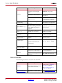
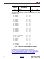
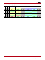
Revision History
The following table shows the revision history for this document.
Date
Version
07/15/2009
1.0
Initial Xilinx release.
08/19/2009
1.1
•
•
•
•
•
UG518 (v1.1) August 19, 2009
Revision
Added Appendix C, “VITA 57.1 FMC Connections.”
Updated Figure 1-18 and Figure 1-32.
Updated Table 1-4, Table 1-17, and Table 1-20.
Added introductory paragraph to Appendix D, “SP601 Master UCF.”
Miscellaneous typographical edits and new user guide template.
www.xilinx.com
SP601 Hardware User Guide
SP601 Hardware User Guide
www.xilinx.com
UG518 (v1.1) August 19, 2009
Table of Contents
Preface: About This Guide
Guide Contents . . . . . . . . . . . . . . . . . . . . . . . . . . . . . . . . . . . . . . . . . . . . . . . . . . . . . . . . . . . . . . 7
Additional Resources . . . . . . . . . . . . . . . . . . . . . . . . . . . . . . . . . . . . . . . . . . . . . . . . . . . . . . . . 7
Conventions . . . . . . . . . . . . . . . . . . . . . . . . . . . . . . . . . . . . . . . . . . . . . . . . . . . . . . . . . . . . . . . . . 7
Typographical . . . . . . . . . . . . . . . . . . . . . . . . . . . . . . . . . . . . . . . . . . . . . . . . . . . . . . . . . . . . . 7
Online Document . . . . . . . . . . . . . . . . . . . . . . . . . . . . . . . . . . . . . . . . . . . . . . . . . . . . . . . . . . 8
Chapter 1: SP601 Evaluation Board
Overview . . . . . . . . . . . . . . . . . . . . . . . . . . . . . . . . . . . . . . . . . . . . . . . . . . . . . . . . . . . . . . . . . . . . 9
Additional Information . . . . . . . . . . . . . . . . . . . . . . . . . . . . . . . . . . . . . . . . . . . . . . . . . . . . . 9
Features . . . . . . . . . . . . . . . . . . . . . . . . . . . . . . . . . . . . . . . . . . . . . . . . . . . . . . . . . . . . . . . . . 10
Block Diagram . . . . . . . . . . . . . . . . . . . . . . . . . . . . . . . . . . . . . . . . . . . . . . . . . . . . . . . . . . . 11
Related Xilinx Documents . . . . . . . . . . . . . . . . . . . . . . . . . . . . . . . . . . . . . . . . . . . . . . . . . . . 11
Detailed Description . . . . . . . . . . . . . . . . . . . . . . . . . . . . . . . . . . . . . . . . . . . . . . . . . . . . . . . . 12
1. Spartan-6 XC6SLX16-2CSG324 FPGA . . . . . . . . . . . . . . . . . . . . . . . . . . . . . . . . . . . . . .
Configuration . . . . . . . . . . . . . . . . . . . . . . . . . . . . . . . . . . . . . . . . . . . . . . . . . . . . . . . . .
I/O Voltage Rails . . . . . . . . . . . . . . . . . . . . . . . . . . . . . . . . . . . . . . . . . . . . . . . . . . . . . .
2. 128 MB DDR2 Component Memory . . . . . . . . . . . . . . . . . . . . . . . . . . . . . . . . . . . . . . .
3. SPI x4 Flash . . . . . . . . . . . . . . . . . . . . . . . . . . . . . . . . . . . . . . . . . . . . . . . . . . . . . . . . . . . .
4. Linear Flash BPI . . . . . . . . . . . . . . . . . . . . . . . . . . . . . . . . . . . . . . . . . . . . . . . . . . . . . . . .
5. 10/100/1000 Tri-Speed Ethernet PHY . . . . . . . . . . . . . . . . . . . . . . . . . . . . . . . . . . . . .
6. USB-to-UART Bridge . . . . . . . . . . . . . . . . . . . . . . . . . . . . . . . . . . . . . . . . . . . . . . . . . . . .
7. IIC Bus . . . . . . . . . . . . . . . . . . . . . . . . . . . . . . . . . . . . . . . . . . . . . . . . . . . . . . . . . . . . . . . .
8-Kb NV Memory . . . . . . . . . . . . . . . . . . . . . . . . . . . . . . . . . . . . . . . . . . . . . . . . . . . . . .
8. Clock Generation . . . . . . . . . . . . . . . . . . . . . . . . . . . . . . . . . . . . . . . . . . . . . . . . . . . . . . .
Oscillator (Differential) . . . . . . . . . . . . . . . . . . . . . . . . . . . . . . . . . . . . . . . . . . . . . . . . . .
Oscillator Socket (Single-Ended, 2.5V or 3.3V) . . . . . . . . . . . . . . . . . . . . . . . . . . . . . . . .
SMA Connectors (Differential) . . . . . . . . . . . . . . . . . . . . . . . . . . . . . . . . . . . . . . . . . . . .
9. VITA 57.1 FMC-LPC Connector . . . . . . . . . . . . . . . . . . . . . . . . . . . . . . . . . . . . . . . . . .
10. Status LEDs . . . . . . . . . . . . . . . . . . . . . . . . . . . . . . . . . . . . . . . . . . . . . . . . . . . . . . . . . . .
11. FPGA Awake LED and Suspend Jumper . . . . . . . . . . . . . . . . . . . . . . . . . . . . . . . . . .
12. FPGA INIT and DONE LEDs . . . . . . . . . . . . . . . . . . . . . . . . . . . . . . . . . . . . . . . . . . . .
13. User I/O . . . . . . . . . . . . . . . . . . . . . . . . . . . . . . . . . . . . . . . . . . . . . . . . . . . . . . . . . . . . .
14. FPGA_PROG_B Pushbutton Switch . . . . . . . . . . . . . . . . . . . . . . . . . . . . . . . . . . . . . .
13
13
13
14
18
20
23
25
26
27
27
27
28
28
28
32
33
34
35
40
Power Management . . . . . . . . . . . . . . . . . . . . . . . . . . . . . . . . . . . . . . . . . . . . . . . . . . . . . . . . . 40
AC Adapter and 5V Input Power Jack/Switch . . . . . . . . . . . . . . . . . . . . . . . . . . . . . . . . 40
Onboard Power Supplies . . . . . . . . . . . . . . . . . . . . . . . . . . . . . . . . . . . . . . . . . . . . . . . . . . 40
Configuration Options . . . . . . . . . . . . . . . . . . . . . . . . . . . . . . . . . . . . . . . . . . . . . . . . . . . . . . 42
JTAG Configuration. . . . . . . . . . . . . . . . . . . . . . . . . . . . . . . . . . . . . . . . . . . . . . . . . . . . . . . 42
SP601 Hardware User Guide
UG518 (v1.1) August 19, 2009
www.xilinx.com
5
Appendix A: References
Appendix B: Default Jumper and Switch Settings
Appendix C: VITA 57.1 FMC Connections
Appendix D: SP601 Master UCF
6
www.xilinx.com
SP601 Hardware User Guide
UG518 (v1.1) August 19, 2009
Preface
About This Guide
This manual accompanies the Spartan®-6 FPGA SP601 Evaluation Board and contains
information about the SP601 hardware and software tools.
Guide Contents
This manual contains the following chapters:
•
Chapter 1, “SP601 Evaluation Board,” provides an overview of the embedded
development board and details the components and features of the SP601 board.
•
Appendix A, “References.”
•
Appendix B, “Default Jumper and Switch Settings.”
•
Appendix D, “SP601 Master UCF.”
Additional Resources
To search the database of silicon and software questions and answers, or to create a
technical support case in WebCase, see the Xilinx website at:
http://www.xilinx.com/support.
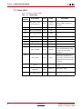
Conventions
This document uses the following conventions. An example illustrates each convention.
Typographical
The following typographical conventions are used in this document:
Convention
Meaning or Use
Example
Courier font
Messages, prompts, and
program files that the system
displays
speed grade: - 100
Courier bold
Literal commands that you enter
in a syntactical statement
ngdbuild design_name
Commands that you select from
a menu
File → Open
Keyboard shortcuts
Ctrl+C
Helvetica bold
SP601 Hardware User Guide
UG518 (v1.1) August 19, 2009
www.xilinx.com
7
Preface: About This Guide
Convention
Meaning or Use
Example
Variables in a syntax statement
for which you must supply
values
ngdbuild design_name
References to other manuals
See the User Guide for more
information.
Emphasis in text
If a wire is drawn so that it
overlaps the pin of a symbol, the
two nets are not connected.
Dark Shading
Items that are not supported or
reserved
This feature is not supported
Square brackets
An optional entry or parameter.
However, in bus specifications,
such as bus[7:0], they are
required.
ngdbuild [option_name]
design_name
A list of items from which you
must choose one or more
lowpwr ={on|off}
Separates items in a list of
choices
lowpwr ={on|off}
User-defined variable or in code
samples
<directory name>
Vertical ellipsis
.
.
.
Repetitive material that has
been omitted
IOB #1: Name = QOUT’
IOB #2: Name = CLKIN’
.
.
.
Horizontal ellipsis . . .
Repetitive material that has
been omitted
allow block block_name loc1
loc2 ... locn;
The prefix ‘0x’ or the suffix ‘h’
indicate hexadecimal notation
A read of address 0x00112975
returned 45524943h.
An ‘_n’ means the signal is
active low
usr_teof_n is active low.
Italic font
Braces
[ ]
{ }
Vertical bar
|
Angle brackets < >
Notations
Online Document
The following conventions are used in this document:
Convention
8
Meaning or Use
Blue text
Cross-reference link to a location
in the current document
Blue, underlined text
Hyperlink to a website (URL)
www.xilinx.com
Example
See the section “Additional
Resources” for details.
Refer to “Title Formats” in
Chapter 1 for details.
Go to http://www.xilinx.com
for the latest speed files.
SP601 Hardware User Guide
UG518 (v1.1) August 19, 2009
Chapter 1
SP601 Evaluation Board
Overview
The SP601 board enables hardware and software developers to create or evaluate designs
targeting the Spartan®-6 XC6SLX16-2CSG324 FPGA.
The SP601 provides board features for evaluating the Spartan-6 family that are common to
most entry-level development environments. Some commonly used features include a
DDR2 memory controller, a parallel linear flash, a tri-mode Ethernet PHY, generalpurpose I/O (GPIO), and a UART. Additional functionality can be added through the
VITA 57.1.1 expansion connector. “Features,” page 10 provides a general listing of the
board features with details provided in “Detailed Description,” page 12.
Additional Information
Additional information and support material is located at:
•
http://www.xilinx.com/sp601
This information includes:
•
Current version of this user guide in PDF format
•
Example design files for demonstration of Spartan-6 FPGA features and technology
•
Demonstration hardware and software configuration files for the SP601 linear and SPI
memory devices
•
Reference Design Files
•
Schematics in PDF format and DxDesigner schematic format
•
Bill of materials (BOM)
•
Printed-circuit board (PCB) layout in Allegro PCB format
•
Gerber files for the PCB (Many free or shareware Gerber file viewers are available on
the internet for viewing and printing these files.)
•
Additional documentation, errata, frequently asked questions, and the latest news
For information about the Spartan-6 family of FPGA devices, including product
highlights, data sheets, user guides, and application notes, see the Spartan-6 FPGA website
at http://www.xilinx.com/support/documentation/spartan-6.htm.
SP601 Hardware User Guide
UG518 (v1.1) August 19, 2009
www.xilinx.com
9
Chapter 1: SP601 Evaluation Board
Features
The SP601 board provides the following features:
•
1. Spartan-6 XC6SLX16-2CSG324 FPGA
•
2. 128 MB DDR2 Component Memory
•
3. SPI x4 Flash
•
4. Linear Flash BPI
•
5. 10/100/1000 Tri-Speed Ethernet PHY
•
7. IIC Bus
•
8Kb NV memory
♦
External access 2-pin header
♦
VITA 57.1 FMC-LPC connector
8. Clock Generation
♦
Oscillator (Differential)
♦
Oscillator Socket (Single-Ended, 2.5V or 3.3V)
•
SMA Connectors (Differential)
•
9. VITA 57.1 FMC-LPC Connector
•
10. Status LEDs
•
♦
FPGA_AWAKE
♦
INIT
♦
DONE
13. User I/O
♦
User LEDs
♦
User DIP switch
♦
User pushbuttons
♦
GPIO male pin header
•
14. FPGA_PROG_B Pushbutton Switch
•
Configuration Options
•
10
♦
♦
3. SPI x4 Flash (both onboard and off-board)
♦
4. Linear Flash BPI
♦
JTAG Configuration
Power Management - AC Adapter and 5V Input Power Jack/Switch, Onboard Power
Supplies
www.xilinx.com
SP601 Hardware User Guide
UG518 (v1.1) August 19, 2009
Related Xilinx Documents
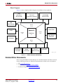
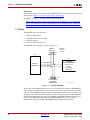
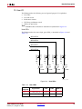
Block Diagram
Figure 1-1 shows a high-level block diagram of the SP601 and its peripherals.
X-Ref Target - Figure 1-1
LEDs
DIP Switch
GPIO Header
USB
JTAG Connector
FMC LPC
Expansion Connector
10/100/1000
Ethernet GMII
DED
Bank 0
2.5 V
Parallel Flash
Spartan-6
DDR2
Bank 3
1.8V
XC6SLX16
Bank 1
2.5V
U1
Differential Clock
Clock Socket
SMA Clock
Pushbuttons
Bank 2
2.5V
IIC EEPROM
and Header
MODE
DIP Switch
SPI x4 or
External Config
USB UART
UG518_01_070809
Figure 1-1:
SP601 Features and Banking
Related Xilinx Documents
Prior to using the SP601 Evaluation Board, users should be familiar with Xilinx resources.
See the following locations for additional documentation on Xilinx tools and solutions:
•
ISE: www.xilinx.com/ise
•
Answer Browser: www.xilinx.com/support
•
Intellectual Property: www.xilinx.com/ipcenter
SP601 Hardware User Guide
UG518 (v1.1) August 19, 2009
www.xilinx.com
11
Chapter 1: SP601 Evaluation Board
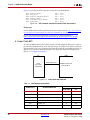
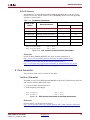
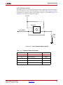
Detailed Description
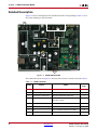
Figure 1-2 shows a board photo with numbered features corresponding to Table 1-1 and
the section headings in this document.
X-Ref Target - Figure 1-2
14
13
15
9
8
2
1
7
16
11
4
8
3
5
12
10
6
13
Figure 1-2:
SP601 Board Photo
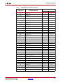
The numbered features in Figure 1-2 correlate to the features and notes listed in Table 1-1.
Table 1-1:
SP601 Features
Number
12
Feature
Schematic
Page
Notes
1
Spartan-6 FPGA
XC6SLX16-2CSG324
2
DDR2 Component
Hard memory controller w/ OCT
5
3
SPI x4 Flash and Headers
SPI select and External Headers
8
4
Linear Flash BPI
StrataFlash 8-bit (J3 device), 3 pins
shared w/ SPI x4
8
5
10/100/1000 Ethernet PHY
GMII Marvell Alaska PHY
7
6
RS232 UART (USB Bridge)
Uses CP2103 Serial-to-USB connection
10
7
IIC
Goes to Header and VITA 57.1 FMC
10
8
Clock, socket, SMA
Differential, Single-Ended, Differential
9
www.xilinx.com
SP601 Hardware User Guide
UG518 (v1.1) August 19, 2009
Detailed Description
Table 1-1:
SP601 Features (Cont’d)
Number
Feature
Notes
Schematic
Page
9
VITA 57.1 FMC-LPC
connector
LVDS signals, clocks, PRSNT
6
10
LEDs
Ethernet PHY Status
7
11
LED, Header
FPGA Awake LED, Suspend Header
8
12
LEDs
FPGA INIT, DONE
9
LED
User I/O (active-High)
9
DIP Switch
User I/O (active-High)
9
Pushbutton
User I/O, CPU_RESET (active-High)
9
12-pin (8 I/O) Header
6 pins x 2 male header with 8 I/Os
(active-High)
10
14
Pushbutton
FPGA_PROG_B
9
15
USB JTAG
Cypress USB to JTAG download cable
logic
16
Onboard Power
Power Management
13
14, 15
11,12,13
1. Spartan-6 XC6SLX16-2CSG324 FPGA
A Xilinx Spartan-6 XC6SLX16-2CSG324 FPGA is installed on the Embedded Development
Board.
Configuration
The SP601 supports configuration in the following modes:
•
Master SPI x4
•
Master SPI x4 with off-board device
•
BPI
•
JTAG (using the included USB-A to Mini-B cable)
For details on configuring the FPGA, see “Configuration Options.”
I/O Voltage Rails
There are four available banks on the LX16-CS324 device. Banks 0, 1, and 2 are connected
for 2.5V I/O. Bank 3 is used for the 1.8V DDR2 component memory interface of Spartan-6
FPGA’s hard memory controller. The voltage applied to the FPGA I/O banks used by the
SP601 board is summarized in Table 1-2.
Table 1-2:
SP601 Hardware User Guide
UG518 (v1.1) August 19, 2009
I/O Voltage Rail of FPGA Banks
FPGA Bank
I/O Voltage Rail
0
2.5V
1
2.5V
www.xilinx.com
13
Chapter 1: SP601 Evaluation Board
Table 1-2:
I/O Voltage Rail of FPGA Banks (Cont’d)
FPGA Bank
I/O Voltage Rail
2
2.5V
3
1.8V
References
See the Xilinx Spartan-6 FPGA documentation for more information at
http://www.xilinx.com/support/documentation/spartan-6.htm.
2. 128 MB DDR2 Component Memory
There are 128 MB of DDR2 memory available on the SP601 board. A 1-Gb Elpida
EDE1116ACBG (84-ball) DDR2 memory component is accessible through Bank 3 of the
LX16 device. The Spartan-6 FPGA hard memory controller is used for data transfer across
the DDR2 memory interface's 16-bit data path using SSTL18 signaling. The maximum data
rate supported is 800 Mb/s with a memory clock running at 400 MHz. Signal integrity is
maintained through DDR2 resistor terminations and memory on-die terminations (ODT),
as shown in Table 1-3 and Table 1-4.
Table 1-3:
Termination Resistor Requirements
Signal Name
Board Termination
DDR2_A[14:0]
49.9 ohms to VTT
DDR2_BA[2:0]
49.9 ohms to VTT
DDR2_RAS_N
49.9 ohms to VTT
DDR2_CAS_N
49.9 ohms to VTT
DDR2_WE_N
49.9 ohms to VTT
DDR2_CS_N
100 ohms to GND
DDR2_CKE
4.7K ohms to GND
DDR2_ODT
4.7K ohms to GND
On-Die Termination
DDR2_DQ[15:0]
ODT
DDR2_UDQS[P,N],
DDR2_LDQS[P,N]
ODT
DDR2_UDM, DDR2_LDM
ODT
DDR2_CK[P,N]
100 ohm differential at
memory component
Notes:
1. Nominal value of VTT for DDR2 interface is 0.9V.
Table 1-4:
14
FPGA On-Chip (OCT) Termination External Resistor Requirements
FPGA U1 Pin
FPGA Pin Number
Board Connection for OCT
ZIO
L6
No Connect
RZQ
C2
100 ohms to GROUND
www.xilinx.com
SP601 Hardware User Guide
UG518 (v1.1) August 19, 2009
Detailed Description
Table 1-5 shows the connections and pin numbers for the DDR2 Component Memory.
Table 1-5:
DDR2 Component Memory Connections
Memory U2
FPGA U1
SP601 Hardware User Guide
UG518 (v1.1) August 19, 2009
Schematic Netname
Pin Number
Name
J7
DDR2_A0
M8
A0
J6
DDR2_A1
M3
A1
H5
DDR2_A2
M7
A2
L7
DDR2_A3
N2
A3
F3
DDR2_A4
N8
A4
H4
DDR2_A5
N3
A5
H3
DDR2_A6
N7
A6
H6
DDR2_A7
P2
A7
D2
DDR2_A8
P8
A8
D1
DDR2_A9
P3
A9
F4
DDR2_A10
M2
A10
D3
DDR2_A11
P7
A11
G6
DDR2_A12
R2
A12
L2
DDR2_DQ0
G8
DQ0
L1
DDR2_DQ1
G2
DQ1
K2
DDR2_DQ2
H7
DQ2
K1
DDR2_DQ3
H3
DQ3
H2
DDR2_DQ4
H1
DQ4
H1
DDR2_DQ5
H9
DQ5
J3
DDR2_DQ6
F1
DQ6
J1
DDR2_DQ7
F9
DQ7
M3
DDR2_DQ8
C8
DQ8
M1
DDR2_DQ9
C2
DQ9
N2
DDR2_DQ10
D7
DQ10
N1
DDR2_DQ11
D3
DQ11
T2
DDR2_DQ12
D1
DQ12
T1
DDR2_DQ13
D9
DQ13
U2
DDR2_DQ14
B1
DQ14
U1
DDR2_DQ15
B9
DQ15
www.xilinx.com
15
Chapter 1: SP601 Evaluation Board
Table 1-5:
DDR2 Component Memory Connections (Cont’d)
Memory U2
FPGA U1
Schematic Netname
Pin Number
Name
F2
DDR2_BA0
L2
BA0
F1
DDR2_BA1
L3
BA1
E1
DDR2_BA2
L1
BA2
E3
DDR2_WE_B
K3
WE
L5
DDR2_RAS_B
K7
RAS
K5
DDR2_CAS_B
L7
CAS
K6
DDR2_ODT
K9
ODT
G3
DDR2_CLK_P
J8
CK
G1
DDR2_CLK_N
K8
CK
H7
DDR2_CKE
K2
CKE
L4
DDR2_LDQS_P
F7
LDQS
L3
DDR2_LDQS_N
E8
LDQS
P2
DDR2_UDQS_P
B7
UDQS
P1
DDR2_UDQS_N
A8
UDQS
K3
DDR2_LDM
F3
LDM
K4
DDR2_UDM
B3
UDM
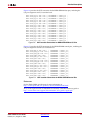
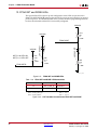
Figure 1-3 provides the user constraints file (UCF) for the DDR2 SDRAM address pins,
including the I/O pin assignment and the I/O standard used.
X-Ref Target - Figure 1-3
NET
NET
NET
NET
NET
NET
NET
NET
NET
NET
NET
NET
NET
"DDR2_A12" LOC ="G6";|
"DDR2_A11" LOC ="D3";|
"DDR2_A10" LOC ="F4";|
"DDR2_A9" LOC ="D1"; |
"DDR2_A8" LOC ="D2"; |
"DDR2_A7" LOC ="H6"; |
"DDR2_A6" LOC ="H3"; |
"DDR2_A5" LOC ="H4"; |
"DDR2_A4" LOC ="F3"; |
"DDR2_A3" LOC ="L7"; |
"DDR2_A2" LOC ="H5"; |
"DDR2_A1" LOC ="J6"; |
"DDR2_A0" LOC ="J7"; |
Figure 1-3:
16
IOSTANDARD
IOSTANDARD
IOSTANDARD
IOSTANDARD
IOSTANDARD
IOSTANDARD
IOSTANDARD
IOSTANDARD
IOSTANDARD
IOSTANDARD
IOSTANDARD
IOSTANDARD
IOSTANDARD
=
=
=
=
=
=
=
=
=
=
=
=
=
SSTL18_II
SSTL18_II
SSTL18_II
SSTL18_II
SSTL18_II
SSTL18_II
SSTL18_II
SSTL18_II
SSTL18_II
SSTL18_II
SSTL18_II
SSTL18_II
SSTL18_II
;
;
;
;
;
;
;
;
;
;
;
;
;
UCF Location Constraints for DDR2 SDRAM Address Inputs
www.xilinx.com
SP601 Hardware User Guide
UG518 (v1.1) August 19, 2009
Detailed Description
Figure 1-4 provides the UCF constraints for the DDR2 SDRAM data pins, including the
I/O pin assignment and I/O standard used.
X-Ref Target - Figure 1-4
NET
NET
NET
NET
NET
NET
NET
NET
NET
NET
NET
NET
NET
NET
NET
NET
"DDR2_DQ15" LOC ="U1";|
"DDR2_DQ14" LOC ="U2";|
"DDR2_DQ13" LOC ="T1";|
"DDR2_DQ12" LOC ="T2";|
"DDR2_DQ11" LOC ="N1";|
"DDR2_DQ10" LOC ="N2";|
"DDR2_DQ9" LOC ="M1"; |
"DDR2_DQ8" LOC ="M3"; |
"DDR2_DQ7" LOC ="J1"; |
"DDR2_DQ6" LOC ="J3"; |
"DDR2_DQ5" LOC ="H1"; |
"DDR2_DQ4" LOC ="H2"; |
"DDR2_DQ3" LOC ="K1"; |
"DDR2_DQ2" LOC ="K2"; |
"DDR2_DQ1" LOC ="L1"; |
"DDR2_DQ0" LOC ="L2"; |
Figure 1-4:
IOSTANDARD
IOSTANDARD
IOSTANDARD
IOSTANDARD
IOSTANDARD
IOSTANDARD
IOSTANDARD
IOSTANDARD
IOSTANDARD
IOSTANDARD
IOSTANDARD
IOSTANDARD
IOSTANDARD
IOSTANDARD
IOSTANDARD
IOSTANDARD
=
=
=
=
=
=
=
=
=
=
=
=
=
=
=
=
SSTL18_II
SSTL18_II
SSTL18_II
SSTL18_II
SSTL18_II
SSTL18_II
SSTL18_II
SSTL18_II
SSTL18_II
SSTL18_II
SSTL18_II
SSTL18_II
SSTL18_II
SSTL18_II
SSTL18_II
SSTL18_II
;
;
;
;
;
;
;
;
;
;
;
;
;
;
;
;
UCF Location Constraints for DDR2 SDRAM Data I/O Pins
Figure 1-5 provides the UCF constraints for the DDR2 SDRAM control pins, including the
I/O pin assignment and the I/O standard used.
X-Ref Target - Figure 1-5
NET
NET
NET
NET
NET
NET
NET
NET
NET
NET
NET
NET
NET
NET
NET
NET
"DDR2_WE_B" LOC ="E3"; |
"DDR2_UDQS_P" LOC ="P2";|
"DDR2_UDQS_N" LOC ="P1";|
"DDR2_UDM" LOC ="K4";
|
"DDR2_RAS_B" LOC ="L5"; |
"DDR2_ODT" LOC ="K6";
|
"DDR2_LDQS_P" LOC ="L4";|
"DDR2_LDQS_N" LOC ="L3";|
"DDR2_LDM" LOC ="K3";
|
"DDR2_CLK_P" LOC ="G3"; |
"DDR2_CLK_N" LOC ="G1"; |
"DDR2_CKE" LOC ="H7";
|
"DDR2_CAS_B" LOC ="K5"; |
"DDR2_BA2" LOC ="E1";
|
"DDR2_BA1" LOC ="F1";
|
"DDR2_BA0" LOC ="F2";
|
Figure 1-5:
IOSTANDARD
IOSTANDARD
IOSTANDARD
IOSTANDARD
IOSTANDARD
IOSTANDARD
IOSTANDARD
IOSTANDARD
IOSTANDARD
IOSTANDARD
IOSTANDARD
IOSTANDARD
IOSTANDARD
IOSTANDARD
IOSTANDARD
IOSTANDARD
=
=
=
=
=
=
=
=
=
=
=
=
=
=
=
=
SSTL18_II
SSTL18_II
SSTL18_II
SSTL18_II
SSTL18_II
SSTL18_II
SSTL18_II
SSTL18_II
SSTL18_II
SSTL18_II
SSTL18_II
SSTL18_II
SSTL18_II
SSTL18_II
SSTL18_II
SSTL18_II
;
;
;
;
;
;
;
;
;
;
;
;
;
;
;
;
UCF Location Constraints for DDR2 SDRAM Control Pins
References
See the Elpida DDR2 specifications for more information at
http://www.elpida.com/en/products/details/EDE1116ACBG.html.
Also, see the Spartan-6 FPGA embedded hard memory controller block user guide at
http://www.xilinx.com/support/documentation/user_guides/ug388.pdf.
SP601 Hardware User Guide
UG518 (v1.1) August 19, 2009
www.xilinx.com
17
Chapter 1: SP601 Evaluation Board
3. SPI x4 Flash
The Xilinx Spartan-6 FPGA hosts a SPI interface which is visible to the Xilinx iMPACT
configuration tool. The SPI memory device operates at 3.0V; the Spartan-6 FPGA I/Os are
3.3V tolerant and provide electrically compatible logic levels to directly access the SPI flash
through a 2.5V bank. The XC6SLX16-2CSG324 is a master device when accessing an
external SPI flash memory device.
The SP601 SPI interface has two parallel connected configuration options (see Figure 1-7):
an SPI X4 (Winbond W25Q64VSFIG) 64-Mb flash memory device and a flash
programming header (J12). J12 supports a user-defined SPI mezzanine board. The SPI
configuration source is selected via SPI select jumper J15. For details on configuring the
FPGA, see “Configuration Options.”
X-Ref Target - Figure 1-6
J12
FPGA_PROG_B
2
FPGA_D2_MISO3
3
FPGA_D1_MISO2
4
SPI_CS_B
TDI
5
FPGA_MOSI_CSI_B_MISO0
TDO
6
FPGA_D0_DIN_MISO_MISO1
TCK
7
FPGA_CCLK
GND
8
GND
9
VCC3V3
TMS
Silkscreen
1
3V3
HDR_1X9
UG518_06_070809
Figure 1-6:
18
J12 SPI Flash Programming Header
www.xilinx.com
SP601 Hardware User Guide
UG518 (v1.1) August 19, 2009
Detailed Description
X-Ref Target - Figure 1-7
U1
FPGA SPI INTERFACE
J12
U17
DIN,DOUT,CCLK
SPI X4
FLASH
MEMORY
SPIX4_CS_B
SPI_CS_B
WINBOND
W25Q64VSFIG
2
ON = SPI X4 U17
OFF = SPI EXT. J12
1
J15
SPI PROGRAM
HEADER
SPI SELECT
JUMPER
UG518_07_070809
Figure 1-7:
Table 1-6:
FPGA U1
Pin
SPI x4 Memory Connections
SPI MEM U17
SPI HDR J12
Schematic Netname
Pin #
Pin Name
Pin #
V2
FPGA_PROG_B
V14
FPGA_D2_MISO3
1
IO3_HOLD_B
2
T14
FPGA_D1_MISO2_R
9
IO2_WP_B
3
V3
SPI_CS_B
T13
FPGA_MOSI_CSI_B_MISO0
15
R13
FPGA_D0_DIN_MISO_MISO1
R15
FPGA_CCLK
J15.2
SP601 Hardware User Guide
UG518 (v1.1) August 19, 2009
SPI Flash Interface Topology
SPIX4_CS_B
1
4
TMS
DIN
5
TDI
8
IO1_DOUT
6
TDO
16
CLK
7
TCK
8
GND
9
VCC3V3
7
www.xilinx.com
Pin Name
CS_B
19
Chapter 1: SP601 Evaluation Board
Figure 1-8 provides the UCF constraints for the SPI serial flash PROM.
X-Ref Target - Figure 1-8
NET
NET
NET
NET
NET
NET
"FPGA_D2_MISO3"
"SPI_CS_B"
"FPGA_D0_DIN_MISO_MISO1"
"FPGA_D1_MISO2"
"FPGA_MOSI_CSI_B_MISO0"
"FPGA_CCLK"
Figure 1-8:
LOC
LOC
LOC
LOC
LOC
LOC
=
=
=
=
=
=
"V14";
"V3";
"R13";
"T14";
"T13";
"R15";
UCF Location Constraints for BPI Flash Connections
References
See the Winbond Serial Flash specifications for more information at http://www.winbondusa.com/hq/enu/ProductAndSales/ProductLines/FlashMemory/SerialFlash/W25X64.htm.
See the XPS Serial Peripheral Interface specification for more information at
http://www.xilinx.com/support/documentation/ip_documentation/xps_spi.pdf.
4. Linear Flash BPI
An 8-bit (16 MB) Numonyx linear flash memory (TE 28F128J3D-75) (J3D type) is used to
provide non-volatile bitstream, code, and data storage. The J3D devices operate at 3.0V; the
Spartan-6 FPGA I/Os are 3.3V tolerant and provide electrically compatible logic levels to
directly access the linear flash BPI through a 2.5V bank. For details on configuring the
FPGA, see “Configuration Options.”
X-Ref Target - Figure 1-9
U1
U10
ADDR, DATA, CTRL
FPGA
BPI FLASH
INTERFACE
NUMONYX TYPE J3vD
T28F128J3D-75
UG518_09_070809
Figure 1-9:
Table 1-7:
Linear Flash BPI Interface
BPI Memory Connections
BPI Memory U10
FPGA U1 Pin
20
Schematic Netname
Pin Number
Pin
K18
FLASH_A0
32
A0
K17
FLASH_A1
28
A1
J18
FLASH_A2
27
A2
J16
FLASH_A3
26
A3
G18
FLASH_A4
25
A4
G16
FLASH_A5
24
A5
www.xilinx.com
SP601 Hardware User Guide
UG518 (v1.1) August 19, 2009
Detailed Description
Table 1-7:
BPI Memory Connections (Cont’d)
BPI Memory U10
FPGA U1 Pin
SP601 Hardware User Guide
UG518 (v1.1) August 19, 2009
Schematic Netname
Pin Number
Pin
H16
FLASH_A6
23
A6
H15
FLASH_A7
22
A7
H14
FLASH_A8
20
A8
H13
FLASH_A9
19
A9
F18
FLASH_A10
18
A10
F17
FLASH_A11
17
A11
K13
FLASH_A12
13
A12
K12
FLASH_A13
12
A13
E18
FLASH_A14
11
A14
E16
FLASH_A15
10
A15
G13
FLASH_A16
8
A16
H12
FLASH_A17
7
A17
D18
FLASH_A18
6
A18
D17
FLASH_A19
5
A19
G14
FLASH_A20
4
A20
F14
FLASH_A21
3
A21
C18
FLASH_A22
1
A22
C17
FLASH_A23
30
A23
F16
FLASH_A24
56
A24
R13
FPGA_D0_DIN_MISO_MISO1
33
DQ0
T14
FPGA_D1_MISO2
35
DQ1
V14
FPGA_D2_MISO3
38
DQ2
U5
FLASH_D3
40
DQ3
V5
FLASH_D4
44
DQ4
R3
FLASH_D5
46
DQ5
T3
FLASH_D6
49
DQ6
R5
FLASH_D7
51
DQ7
M16
FLASH_WE_B
55
WE_B
L18
FLASH_OE_B
54
OE_B
www.xilinx.com
21
Chapter 1: SP601 Evaluation Board
Table 1-7:
BPI Memory Connections (Cont’d)
BPI Memory U10
FPGA U1 Pin
Schematic Netname
Pin Number
Pin
L17
FLASH_CE_B
14
CE0
B3
FMC_PWR_GOOD_FLASH_RST_B
16
RP_B
Note: Memory U10 pin 56 address A24 is not connected on the 16 MB device. It is made available
for larger density devices.
X-Ref Target - Figure 1-10
NET
NET
NET
NET
NET
NET
NET
NET
NET
NET
NET
NET
NET
NET
NET
NET
NET
NET
NET
NET
NET
NET
NET
NET
NET
"FLASH_A0"
"FLASH_A1"
"FLASH_A2"
"FLASH_A3"
"FLASH_A4"
"FLASH_A5"
"FLASH_A6"
"FLASH_A7"
"FLASH_A8"
"FLASH_A9"
"FLASH_A10"
"FLASH_A11"
"FLASH_A12"
"FLASH_A13"
"FLASH_A14"
"FLASH_A15"
"FLASH_A16"
"FLASH_A17"
"FLASH_A18"
"FLASH_A19"
"FLASH_A20"
"FLASH_A21"
"FLASH_A22"
"FLASH_A23"
"FLASH_A24"
LOC
LOC
LOC
LOC
LOC
LOC
LOC
LOC
LOC
LOC
LOC
LOC
LOC
LOC
LOC
LOC
LOC
LOC
LOC
LOC
LOC
LOC
LOC
LOC
LOC
=
=
=
=
=
=
=
=
=
=
=
=
=
=
=
=
=
=
=
=
=
=
=
=
=
"K18";
"K17";
"J18";
"J16";
"G18";
"G16";
"H16";
"H15";
"H14";
"H13";
"F18";
"F17";
"K13";
"K12";
"E18";
"E16";
"G13";
"H12";
"D18";
"D17";
"G14";
"F14";
"C18";
"C17";
"F16";
NET
NET
NET
NET
NET
NET
NET
NET
"FPGA_D0_DIN_MISO_MISO1"
"FPGA_D1_MISO2"
"FPGA_D2_MISO3"
"FLASH_D3"
"FLASH_D4"
"FLASH_D5"
"FLASH_D6"
"FLASH_D7"
LOC
LOC
LOC
LOC
LOC
LOC
LOC
LOC
=
=
=
=
=
=
=
=
"R13";
"T14";
"V14";
"U5";
"V5";
"R3";
"T3";
"R5";
NET
NET
NET
NET
"FLASH_WE_B"
"FLASH_OE_B"
"FLASH_CE_B"
"FMC_PWR_GOOD_FLASH_RST_B"
LOC
LOC
LOC
LOC
=
=
=
=
"M16";
"L18";
"L17";
"B3";
Figure 1-10:
UCF Location Constraints for BPI Flash Connections
References
See the Numonyx Flash Memory specifications for more information at
http://www.numonyx.com/Documents/Datasheets/308551_J3D_Discrete_DS.pdf.
In addition, see the Xilinx Spartan-6 Configuration User Guide for more information at
http://www.xilinx.com/support/documentation/user_guides/ug380.pdf.
22
www.xilinx.com
SP601 Hardware User Guide
UG518 (v1.1) August 19, 2009
Detailed Description
5. 10/100/1000 Tri-Speed Ethernet PHY
The SP601 uses the onboard Marvell Alaska PHY device (88E1111) for Ethernet
communications at 10, 100, or 1000 Mb/s. The board supports a GMII/MII interface from
the FPGA to the PHY. The PHY connection to a user-provided Ethernet cable is through a
Halo HFJ11-1G01E RJ-45 connector with built-in magnetics.
On power-up, or on reset, the PHY is configured to operate in GMII mode with PHY
address 0b00111 using the settings shown in Table 1-8. These settings can be overwritten
via software commands passed over the MDIO interface.
Table 1-8:
Pin
PHY Configuration Pins
Connection on
Bit[2]
Bit[1]
Bit[0]
Board
Definition and Value Definition and Value Definition and Value
CFG0
VCC 2.5V
PHYADR[2] = 1
PHYADR[1] = 1
PHYADR[0] = 1
CFG1
Ground
ENA_PAUSE = 0
PHYADR[4] = 0
PHYADR[3] = 0
CFG2
VCC 2.5V
ANEG[3] = 1
ANEG[2] = 1
ANEG[1] = 1
CFG3
VCC 2.5V
ANEG[0] = 1
ENA_XC = 1
DIS_125 = 1
CFG4
VCC 2.5V
HWCFG_MD[2] = 1
HWCFG_MD[1] = 1
HWCFG_MD[0] = 1
CFG5
VCC 2.5V
DIS_FC = 1
DIS_SLEEP = 1
HWCFG_MD[3] = 1
CFG6
PHY_LED_RX
SEL_BDT = 0
INT_POL = 1
75/50 OHM = 0
Table 1-9:
FPGA U1
Pin
SP601 Hardware User Guide
UG518 (v1.1) August 19, 2009
PHY Connections
Schematic Netname
U3 M88E111
P16
PHY_MDIO
33
N14
PHY_MDC
35
J13
PHY_INT
32
L13
PHY_RESET
36
M13
PHY_CRS
115
L14
PHY_COL
114
L16
PHY_RXCLK
7
P17
PHY_RXER
8
N18
PHY_RXCTL_RXDV
4
M14
PHY_RXD0
3
U18
PHY_RXD1
128
U17
PHY_RXD2
126
T18
PHY_RXD3
125
T17
PHY_RXD4
124
N16
PHY_RXD5
123
N15
PHY_RXD6
121
www.xilinx.com
23
Chapter 1: SP601 Evaluation Board
Table 1-9:
FPGA U1
Pin
PHY Connections (Cont’d)
Schematic Netname
P18
PHY_RXD7
120
A9
PHY_TXC_GTXCLK
14
B9
PHY_TXCLK
10
A8
PHY_TXER
13
B8
PHY_TXCTL_TXEN
16
F8
PHY_TXD0
18
G8
PHY_TXD1
19
A6
PHY_TXD2
20
B6
PHY_TXD3
24
E6
PHY_TXD4
25
F7
PHY_TXD5
26
A5
PHY_TXD6
28
C5
PHY_TXD7
29
X-Ref Target - Figure 1-11
NET
NET
NET
NET
NET
NET
NET
NET
NET
NET
NET
NET
NET
NET
NET
NET
NET
NET
NET
NET
NET
NET
NET
NET
NET
NET
NET
NET
NET
"PHY_COL"
"PHY_CRS"
"PHY_INT"
"PHY_MDC"
"PHY_MDIO"
"PHY_RESET"
"PHY_RXCLK"
"PHY_RXCTL_RXDV"
"PHY_RXD0"
"PHY_RXD1"
"PHY_RXD2"
"PHY_RXD3"
"PHY_RXD4"
"PHY_RXD5"
"PHY_RXD6"
"PHY_RXD7"
"PHY_RXER"
"PHY_TXCLK"
"PHY_TXCTL_TXEN"
"PHY_TXC_GTXCLK"
"PHY_TXD0"
"PHY_TXD1"
"PHY_TXD2"
"PHY_TXD3"
"PHY_TXD4"
"PHY_TXD5"
"PHY_TXD6"
"PHY_TXD7"
"PHY_TXER"
Figure 1-11:
24
U3 M88E111
LOC
LOC
LOC
LOC
LOC
LOC
LOC
LOC
LOC
LOC
LOC
LOC
LOC
LOC
LOC
LOC
LOC
LOC
LOC
LOC
LOC
LOC
LOC
LOC
LOC
LOC
LOC
LOC
LOC
=
=
=
=
=
=
=
=
=
=
=
=
=
=
=
=
=
=
=
=
=
=
=
=
=
=
=
=
=
"L14";
"M13";
"J13";
"N14";
"P16";
"L13";
"L16";
"N18";
"M14";
"U18";
"U17";
"T18";
"T17";
"N16";
"N15";
"P18";
"P17";
"B9";
"B8";
"A9";
"F8";
"G8";
"A6";
"B6";
"E6";
"F7";
"A5";
"C5";
"A8";
UCF Location Constraints for PHY Connections
www.xilinx.com
SP601 Hardware User Guide
UG518 (v1.1) August 19, 2009
Detailed Description
References
See the Marvell Alaska Gigabit Ethernet Transceiver product page for more information at
http://www.marvell.com/products/transceivers/alaska_gigabit/index.jsp.
Also, see the Xilinx Tri-Mode Ethernet MAC User Guide at
http://www.xilinx.com/support/documentation/ip_documentation/tri_mode_eth_ma
c_ug138.pdf.
6. USB-to-UART Bridge
The SP601 contains a Silicon Labs CP2103GM USB-to-UART bridge device (U4) which
allows connection to a host computer with a USB cable. The USB cable is supplied in this
evaluation kit (Type A end to host computer, Type Mini-B end to SP601 connector J9).
Table 1-10 details the SP601 J9 pinout.
Xilinx UART IP is expected to be implemented in the FPGA fabric. The FPGA supports the
USB-to-UART bridge using four signal pins, transmit (TX), receive (RX), Request to Send
(RTS), and Clear to Send (CTS).
Silicon Labs provides royalty-free Virtual COM Port (VCP) drivers which permit the
CP2103GM USB-to-UART bridge to appear as a COM port to host computer
communications application software (for example, HyperTerm or TeraTerm). The VCP
device driver must be installed on the host PC prior to establishing communications with
the SP601. Refer to the SP601 Getting Started Guide for driver installation instructions.
Table 1-10:
USB Type B Pin Assignments and Signal Definitions
USB Connector
Pin
Signal Name
Description
1
VBUS
+5V from host system (not used)
2
USB_DATA_N
Bidirectional differential serial data (N-side)
3
USB_DATA_P
Bidirectional differential serial data (P-side)
4
GROUND
Signal ground
Table 1-11:
FPGA U1
Pin
CP2103GM Connections
Schematic Netname
U10
USB_1_CTS
22
T5
USB_1_RTS
23
L12
USB_1_RX
24
K14
USB_1_TX
25
X-Ref Target - Figure 1-12
NET
NET
NET
NET
"USB_1_CTS"
"USB_1_RTS"
"USB_1_RX"
"USB_1_TX"
Figure 1-12:
SP601 Hardware User Guide
UG518 (v1.1) August 19, 2009
U4 CP2103GM
LOC
LOC
LOC
LOC
=
=
=
=
"U10";
"T5";
"L12";
"K14";
UCF Location Constraints for CP2103GM Connections
www.xilinx.com
25
Chapter 1: SP601 Evaluation Board
References
Technical information on the Silicon Labs CP2103GM and the VCP drivers can be found on
their website at https://www.silabs.com/Pages/default.aspx.
In addition, see some of the Xilinx UART IP specifications at:
•
•
•
http://www.xilinx.com/support/documentation/ip_documentation/opb_uartlite.pdf
http://www.xilinx.com/support/documentation/ip_documentation/xps_uartlite.pdf
http://www.xilinx.com/support/documentation/ip_documentation/xps_uart16550.pdf
7. IIC Bus
The SP601 IIC bus hosts four items:
•
FPGA U1 IIC interface
•
2-pin IIC external access header
•
8-Kb NV Memory
•
VITA 57.1 FMC Connector J1
The SP601 IIC bus topology is shown in Figure 1-13.
X-Ref Target - Figure 1-13
FMC-LPC
GA0=1
GA1=0
VITA 57.1
FMC-LPC
U1
J1
C31
C30
U7
FPGA IIC
INTERFACE
ST MICRO
M24 C08-WDW6TP
IIC_SDA_MAIN
Address range
54-56
0b10101000b1010110
IIC_SCL_MAIN
2
1
J16
IIC EXTERNAL
ACCESS
CONNECTOR
Figure 1-13:
UG518_13_070809
IIC Bus Topology
The IIC Bus on the SP601 provides access to a 2-pin header, the onboard 8-Kb EEPROM,
and the VITA 57.1 FMC interface. The user must ensure there are no IIC address conflicts
with the onboard EEPROM address when attaching additional IIC devices via FMC or the
IIC 2-pin header. Note that FMC Mezzanine cards are designed with 2-Kb IIC EEPROMs
and will not conflict with the Carrier Card (SP601) 8-Kb EEPROM address range. This is
because 2-Kb EEPROMs reside below the 8-Kb EEPROM space. See the VITA 57.1
specification along with any IIC 2-Kbit EEPROM data sheet for more details.
26
www.xilinx.com
SP601 Hardware User Guide
UG518 (v1.1) August 19, 2009
Detailed Description
8-Kb NV Memory
The SP601 hosts a 8-Kb ST Microelectronics M24C08-WDW6TP IIC parameter storage
memory device (U7). The IIC address of U7 is 0b1010100, and U7 is not write protected
(WP pin 7 is tied to GND).
Table 1-12:
IIC Memory Connections
SPI Memory U7
FPGA U1 Pin
Number
Schematic Netname
Pin Number
Pin
Not Applicable
Tied to GND
1
A0
Not Applicable
Tied to GND
2
A1
Not Applicable
Pulled up (0 ohm) to VCC3V3
3
A2
N10
IIC_SDA_MAIN
5
SDA
P11
IIC_SCL_MAIN
6
SCL
Tied to GND
7
WP
Not Applicable
X-Ref Target - Figure 1-14
NET "IIC_SCL_MAIN"
NET "IIC_SDA_MAIN"
Figure 1-14:
LOC = "P11";
LOC = "N10";
UCF Location Constraints for IIC Connections
References
See the ST Micro M24C08-WDW6TP data sheet for more information at
http://www.st.com/stonline/products/literature/ds/5067/m24c08-w.pdf.
In addition, see the Xilinx XPS IIC Bus Interface specification at
http://www.xilinx.com/support/documentation/ip_documentation/xps_iic.pdf.
Also, see “9. VITA 57.1 FMC-LPC Connector,” page 28.
8. Clock Generation
There are three clock sources available on the SP601.
Oscillator (Differential)
The SP601 has one 2.5V LVDS differential 200 MHz oscillator (U5) soldered onto the board
and wired to an FPGA global clock input.
•
Crystal oscillator: Epson EG2121CA
•
PPM frequency jitter: 50 ppm
X-Ref Target - Figure 1-15
NET "SYSCLK_N"
NET "SYSCLK_P"
Figure 1-15:
LOC = "K16";
LOC = "K15";
UCF Location Constraints for Oscillator Connections
References
For more details, see the Epson data sheet at
http://www.epsontoyocom.co.jp/english/product/OSC/set04/eg2121ca/index.html.
SP601 Hardware User Guide
UG518 (v1.1) August 19, 2009
www.xilinx.com
27
Chapter 1: SP601 Evaluation Board
Oscillator Socket (Single-Ended, 2.5V or 3.3V)
One populated single-ended clock socket (X2) is provided for user applications. The option
of 3.3V or 2.5V power may be selected via a 0 ohm resistor selection. The SP601 board is
shipped with a 27MHz 2.5V oscillator installed.
X-Ref Target - Figure 1-16
NET "USER_CLOCK"
Figure 1-16:
LOC = "V10";
UCF Location Constraints for Oscillator Socket Connections
SMA Connectors (Differential)
A high-precision clock signal can be provided to the FPGA using differential clock signals
through the onboard 50-ohm SMA connectors J7(P)/J8(N).
X-Ref Target - Figure 1-17
NET "SMACLK_N"
NET "SMACLK_P"
Figure 1-17:
LOC = "H18";
LOC = "H17";
UCF Location Constraints for SMA Connectors Connections
9. VITA 57.1 FMC-LPC Connector
The VITA 57.1 FMC expansion connector (J1) on the SP601 implements the VITA 57.1.1 LPC
format of the VITA 57.1 FMC standard specification. The VITA 57.1 FMC-LPC connector
provides 68 single-ended (34 differential) user-defined signals (Table 1-13). The VITA 57.1
FMC standard calls for two connector densities: a High Pin Count (HPC) and a Low Pin
Count (LPC) implementation. A common 10 x 40 position (400 pin locations) connector
form factor is used for both versions. The HPC version has 400 pins present, the LPC
version, 160 pins. The Samtec connector system is rated for signaling speeds up to 9 GHz
(18 Gb/s) based on a -3dB insertion loss point within a two-level signaling environment.
Refer to the Samtec website for data sheets and characterization information for the RoHScompliant VITA 57.1 FMC-LPC connector (ASP-134603-01) and its mate.
Note that the SP601 board FMC-LPC connector J1 VADJ voltage is FIXED at 2.5V (nonadjustable). This rail cannot be turned off. The SP601 VITA 57.1 FMC interface is
compatible with 2.5V Mezzanine Cards capable of supporting 2.5V VADJ.
The SP601 supports all FMC LA Bus connections available on the FMC LPC connector,
(LA[00:33]) along with all available FMC M2C clock pairs (CLK0_M2C_P/N and
CLK1_M2C_P/N). The SP601 does not support the FMC DP Bus connections since the
SP601 does not support any Gigabit Transceivers on the FMC DP Bus. Therefore,
DP0_C2M_P/N, DP0_M2C_P/N and GBTCLK0_M2C_P/N are not supported by the
SP601 FMC interface.
For more details about FMC, see the VITA57.1 specification available at
http://www.vita.com/fmc.html.
28
www.xilinx.com
SP601 Hardware User Guide
UG518 (v1.1) August 19, 2009
Detailed Description
Table 1-13:
LPC Pinout
K
J
H
G
F
E
D
C
B
A
1
NC
NC
VREF_A_M2C
GND
NC
NC
PG_C2M
GND
NC
NC
2
NC
NC
PRSNT_M2C_L
CLK1_M2C_P
NC
NC
GND
DP0_C2M_P
NC
NC
3
NC
NC
GND
CLK1_M2C_N
NC
NC
GND
DP0_C2M_N
NC
NC
4
NC
NC
CLK0_M2C_P
GND
NC
NC
GBTCLK0_M2C_P
GND
NC
NC
5
NC
NC
CLK0_M2C_N
GND
NC
NC
GBTCLK0_M2C_N
GND
NC
NC
6
NC
NC
GND
LA00_P_CC
NC
NC
GND
DP0_M2C_P
NC
NC
7
NC
NC
LA02_P
LA00_N_CC
NC
NC
GND
DP0_M2C_N
NC
NC
8
NC
NC
LA02_N
GND
NC
NC
LA01_P_CC
GND
NC
NC
9
NC
NC
GND
LA03_P
NC
NC
LA01_N_CC
GND
NC
NC
10
NC
NC
LA04_P
LA03_N
NC
NC
GND
LA06_P
NC
NC
11
NC
NC
LA04_N
GND
NC
NC
LA05_P
LA06_N
NC
NC
12
NC
NC
GND
LA08_P
NC
NC
LA05_N
GND
NC
NC
13
NC
NC
LA07_P
LA08_N
NC
NC
GND
GND
NC
NC
14
NC
NC
LA07_N
GND
NC
NC
LA09_P
LA10_P
NC
NC
15
NC
NC
GND
LA12_P
NC
NC
LA09_N
LA10_N
NC
NC
16
NC
NC
LA11_P
LA12_N
NC
NC
GND
GND
NC
NC
17
NC
NC
LA11_N
GND
NC
NC
LA13_P
GND
NC
NC
18
NC
NC
GND
LA16_P
NC
NC
LA13_N
LA14_P
NC
NC
19
NC
NC
LA15_P
LA16_N
NC
NC
GND
LA14_N
NC
NC
20
NC
NC
LA15_N
GND
NC
NC
LA17_P_CC
GND
NC
NC
21
NC
NC
GND
LA20_P
NC
NC
LA17_N_CC
GND
NC
NC
22
NC
NC
LA19_P
LA20_N
NC
NC
GND
LA18_P_CC
NC
NC
23
NC
NC
LA19_N
GND
NC
NC
LA23_P
LA18_N_CC
NC
NC
24
NC
NC
GND
LA22_P
NC
NC
LA23_N
GND
NC
NC
25
NC
NC
LA21_P
LA22_N
NC
NC
GND
GND
NC
NC
26
NC
NC
LA21_N
GND
NC
NC
LA26_P
LA27_P
NC
NC
27
NC
NC
GND
LA25_P
NC
NC
LA26_N
LA27_N
NC
NC
28
NC
NC
LA24_P
LA25_N
NC
NC
GND
GND
NC
NC
29
NC
NC
LA24_N
GND
NC
NC
TCK
GND
NC
NC
30
NC
NC
GND
LA29_P
NC
NC
TDI
SCL
NC
NC
31
NC
NC
LA28_P
LA29_N
NC
NC
TDO
SDA
NC
NC
32
NC
NC
LA28_N
GND
NC
NC
3P3VAUX
GND
NC
NC
33
NC
NC
GND
LA31_P
NC
NC
TMS
GND
NC
NC
SP601 Hardware User Guide
UG518 (v1.1) August 19, 2009
www.xilinx.com
29
Chapter 1: SP601 Evaluation Board
Table 1-13:
LPC Pinout (Cont’d)
K
J
H
G
F
E
D
C
B
A
34
NC
NC
LA30_P
LA31_N
NC
NC
TRST_L
GA0
NC
NC
35
NC
NC
LA30_N
GND
NC
NC
GA1
12P0V
NC
NC
36
NC
NC
GND
LA33_P
NC
NC
3P3V
GND
NC
NC
37
NC
NC
LA32_P
LA33_N
NC
NC
GND
12P0V
NC
NC
38
NC
NC
LA32_N
GND
NC
NC
3P3V
GND
NC
NC
39
NC
NC
GND
VADJ
NC
NC
GND
3P3V
NC
NC
40
NC
NC
VADJ
GND
NC
NC
3P3V
GND
NC
NC
30
www.xilinx.com
SP601 Hardware User Guide
UG518 (v1.1) August 19, 2009
Detailed Description
X-RefNET
Target
- Figure 1-18
"FMC_CLK0_M2C_N"
NET "FMC_CLK0_M2C_P"
NET "FMC_CLK1_M2C_N"
NET "FMC_CLK1_M2C_P"
NET "FMC_LA00_CC_N"
NET "FMC_LA00_CC_P"
NET "FMC_LA01_CC_N"
NET "FMC_LA01_CC_P"
NET "FMC_LA02_N"
NET "FMC_LA02_P"
NET "FMC_LA03_N"
NET "FMC_LA03_P"
NET "FMC_LA04_N"
NET "FMC_LA04_P"
NET "FMC_LA05_N"
NET "FMC_LA05_P"
NET "FMC_LA06_N"
NET "FMC_LA06_P"
NET "FMC_LA07_N"
NET "FMC_LA07_P"
NET "FMC_LA08_N"
NET "FMC_LA08_P"
NET "FMC_LA09_N"
NET "FMC_LA09_P"
NET "FMC_LA10_N"
NET "FMC_LA10_P"
NET "FMC_LA11_N"
NET "FMC_LA11_P"
NET "FMC_LA12_N"
NET "FMC_LA12_P"
NET "FMC_LA13_N"
NET "FMC_LA13_P"
NET "FMC_LA14_N"
NET "FMC_LA14_P"
NET "FMC_LA15_N"
NET "FMC_LA15_P"
NET "FMC_LA16_N"
NET "FMC_LA16_P"
NET "FMC_LA17_CC_N"
NET "FMC_LA17_CC_P"
NET "FMC_LA18_CC_N"
NET "FMC_LA18_CC_P"
NET "FMC_LA19_N"
NET "FMC_LA19_P"
NET "FMC_LA20_N"
NET "FMC_LA20_P"
NET "FMC_LA21_N"
NET "FMC_LA21_P"
NET "FMC_LA22_N"
NET "FMC_LA22_P"
NET "FMC_LA23_N"
NET "FMC_LA23_P"
NET "FMC_LA24_N"
NET "FMC_LA24_P"
NET "FMC_LA25_N"
NET "FMC_LA25_P"
NET "FMC_LA26_N"
NET "FMC_LA26_P"
NET "FMC_LA27_N"
NET "FMC_LA27_P"
NET "FMC_LA28_N"
NET "FMC_LA28_P"
NET "FMC_LA29_N"
NET "FMC_LA29_P"
NET "FMC_LA30_N"
NET "FMC_LA30_P"
NET "FMC_LA31_N"
NET "FMC_LA31_P"
NET "FMC_LA32_N"
NET "FMC_LA32_P"
NET "FMC_LA33_N"
NET "FMC_LA33_P"
NET "FMC_PRSNT_M2C_L"
NET "FMC_PWR_GOOD_FLASH_RST_B"
LOC
LOC
LOC
LOC
LOC
LOC
LOC
LOC
LOC
LOC
LOC
LOC
LOC
LOC
LOC
LOC
LOC
LOC
LOC
LOC
LOC
LOC
LOC
LOC
LOC
LOC
LOC
LOC
LOC
LOC
LOC
LOC
LOC
LOC
LOC
LOC
LOC
LOC
LOC
LOC
LOC
LOC
LOC
LOC
LOC
LOC
LOC
LOC
LOC
LOC
LOC
LOC
LOC
LOC
LOC
LOC
LOC
LOC
LOC
LOC
LOC
LOC
LOC
LOC
LOC
LOC
LOC
LOC
LOC
LOC
LOC
LOC
LOC
LOC
=
=
=
=
=
=
=
=
=
=
=
=
=
=
=
=
=
=
=
=
=
=
=
=
=
=
=
=
=
=
=
=
=
=
=
=
=
=
=
=
=
=
=
=
=
=
=
=
=
=
=
=
=
=
=
=
=
=
=
=
=
=
=
=
=
=
=
=
=
=
=
=
=
=
"A10";
"C10";
"V9";
"T9";
"C9";
"D9";
"C11";
"D11";
"A15";
"C15";
"A13";
"C13";
"A16";
"B16";
"A14";
"B14";
"C12";
"D12";
"E8";
"E7";
"E11";
"F11";
"F10";
"G11";
"C8";
"D8";
"A12";
"B12";
"C6";
"D6";
"A11";
"B11";
"A2";
"B2";
"F9";
"G9";
"A7";
"C7";
"T8";
"R8";
"T10";
"R10";
"P7";
"N6";
"P8";
"N7";
"V4";
"T4";
"T7";
"R7";
"P6";
"N5";
"V8";
"U8";
"N11";
"M11";
"V7";
"U7";
"T11";
"R11";
"V11";
"U11";
"N8";
"M8";
"V12";
"T12";
"V6";
"T6";
"V15";
"U15";
"N9";
"M10";
"U13";
"B3";
Figure 1-18: UCF Location Constraints for VITA 57.1 FMC-LPC Connections
SP601 Hardware User Guide
UG518 (v1.1) August 19, 2009
www.xilinx.com
31
Chapter 1: SP601 Evaluation Board
10. Status LEDs
Table 1-14 defines the status LEDs.
Table 1-14:
Reference
Designator
Status LEDs
Signal Name
Color
Label
FMC_PWR_GOOD_
FLASH_RST_B
Green
PWR
GOOD
DS2
PHY_LED_LINK10
Green
10
DS3
PHY_LED_LINK100
Green
100
DS4
PHY_LED_LINK100
0
Green
1000
DS5
PHY_LED_DUPLEX
Green
DUP
DS6
PHY_LED_RX
Green
RX
DS7
PHY_LED_TX
Green
TX
DS8
FPGA_AWAKE
Green
AWAKE
DS1
Green
DONE
INIT
Illuminates after power-up to
indicate that the FPGA has
successfully powered up and
completed its internal poweron process.
DS10
DS15
DS16
DS17
32
FPGA_INIT
Red
VCC5
Green
LED_GRN,
LED_RED
Green/
Red
LTC_PWR_GOOD
Green
www.xilinx.com
Indicates power available for
VITA 57.1 FMC expansion
connector.
Illuminates to indicate the
status of the DONE pin when
the FPGA is successfully
configured.
DS9
FPGA_DONE
Description
Illuminates when 5V supply is
applied.
STATUS
USB to JTAG logic.
Illuminates to indicate that the
board power is good.
SP601 Hardware User Guide
UG518 (v1.1) August 19, 2009
Detailed Description
11. FPGA Awake LED and Suspend Jumper
The suspend mode jumper permits the FPGA to enter an inactive, "suspend" mode. The
FPGA Awake LED DS8 will go out when the FPGA enters this mode.
X-Ref Target - Figure 1-19
FPGA AWAKE
2
VCC2V5
DS8
LED-GRN-SMT
FPGA SUSPEND
1
1
2
J14
2
OFF = AWAKE (default)
ON = SUSPEND
1
R88
27.4
1%
1/16W
2
1
R18
4.7K
5%
1/16W
H-1X2
J14 Suspend Jumper
UG518_19_070809
Figure 1-19:
Table 1-15:
FPGA Awake LED and Suspend Jumper
FPGA Awake/Suspend Mode Jumper Connections
FPGA U1 Pin
Schematic Netname
Suspend Mode I/O
P15
FPGA_AWAKE
Awake LED DS8.2
R16
FPGA_SUSPEND
Suspend J14.2
X-Ref Target - Figure 1-20
NET "FPGA_AWAKE"
NET "FPGA_SUSPEND"
Figure 1-20:
LOC = "P15";
LOC = "R16";
UCF Location Constraints for FPGA Awake/Suspend Mode Jumper
See the Spartan-6 FPGA Configuration Guide for more information at
http://www.xilinx.com/support/documentation/user_guides/ug380.pdf.
SP601 Hardware User Guide
UG518 (v1.1) August 19, 2009
www.xilinx.com
33
Chapter 1: SP601 Evaluation Board
12. FPGA INIT and DONE LEDs
The typical Xilinx FPGA power up and configuration status LEDs are present on the
SP601. The INIT LED DS10 comes on after the FPGA powers up and completes its internal
power-on process. The DONE LED DS9 comes on after the FPGA programming bitstream
has been downloaded and the FPGA successfully configured.
X-Ref Target - Figure 1-21
VCC2V5
1
R113
332
1%
1/16W
VCC2V5
2
FPGA DONE
2
2
2
FPGA INIT B
R90
27.4
1%
1/16W
1
1
DS9
2
LED-GRN-SMT
R23
4.7K
5%
1/16W
1
1
DS10
INIT_B = 0, LED: ON
INIT_B = 1, LED: OFF
LED-RED-SMT
VCC2V5
1
2
R89
27.4
1%
1/16W
UG518_21_070809
Figure 1-21:
Table 1-16:
FPGA INIT and DONE LEDs
FPGA INIT and DONE LED Connections
FPGA U1 Pin
Schematic Netname Controlled LED
U3
FPGA_INIT_B
DS10 INIT
V17
FPGA_DONE
DS9 DONE
X-Ref Target - Figure 1-22
NET "FPGA_INIT_B"
NET "FPGA_DONE"
LOC = "U3";
LOC = "V17";
Figure 1-22: UCF Location Constraints for FPGA INIT and DONE
34
www.xilinx.com
SP601 Hardware User Guide
UG518 (v1.1) August 19, 2009
Detailed Description
13. User I/O
The SP601 provides the following user and general purpose I/O capabilities:
•
User LEDs
•
User DIP switch
•
Pushbutton switches
•
CPU Reset pushbutton switch
•
GPIO male pin header
Note: All GPIO location constraints are collected in one partial UCF in Figure 1-27.
User LEDs
The SP601 provides four active high, green LEDs, as described in Figure 1-23 and
Table 1-17.
X-Ref Target - Figure 1-23
GPIO LED 3
GPIO LED 2
GPIO LED 1
GPIO LED 0
2
2
1
R93
27.4
1%
1/16W
DS14
1
LED-GRN-SMT
1
1
2
R92
27.4
1%
1/16W
DS13
LED-GRN-SMT
DS12
1
LED-GRN-SMT
DS11
2
1
R91
27.4
1%
1/16W
2
2
2
LED-GRN-SMT
1
1
2
R94
27.4
1%
1/16W
UG518_23_070809
Figure 1-23: User LEDs
Table 1-17:
User LEDs
Reference
Designator
Signal Name
Color
DS11
GPIO_LED_0
Green
E13
DS12
GPIO_LED_1
Green
C14
SP601 Hardware User Guide
UG518 (v1.1) August 19, 2009
www.xilinx.com
Label
FPGA Pin
35
Chapter 1: SP601 Evaluation Board
Table 1-17:
User LEDs (Cont’d)
Reference
Designator
Signal Name
Color
DS13
GPIO_LED_2
Green
C4
DS14
GPIO_LED_3
Green
A4
Label
FPGA Pin
User DIP switch
The SP601 includes an active high four pole DIP switch, as described in Figure 1-24 and
Table 1-18.
X-Ref Target - Figure 1-24
VCC2V5
GPIO_SWITCH_0
GPIO_SWITCH_1
GPIO_SWITCH_2
GPIO_SWITCH_3
1
8
2
7
3
6
4
5
SW8
SDMX-4-X
1
2
1
R22
4.7K
5%
1/16W
2
R21
4.7K
5%
1/16W
1
2
R20
4.7K
5%
1/16W
1
2
R19
4.7K
5%
1/16W
UG518_24_070809
Figure 1-24:
Table 1-18:
User DIP Switch Connections
FPGA U1 Pin
36
User DIP Switch
Schematic Netname
SW8 Pin Number
D14
GPIO_SWITCH_0
1
E12
GPIO_SWITCH_1
2
F12
GPIO_SWITCH_2
3
V13
GPIO_SWITCH_3
4
www.xilinx.com
SP601 Hardware User Guide
UG518 (v1.1) August 19, 2009
Detailed Description
User Pushbutton Switches
The SP601 provides five active high pushbutton switches: SW6, SW4, SW5, SW7 and SW9.
The five pushbuttons all have the same topology as the sample shown in Figure 1-25. Four
pushbuttons are assigned as GPIO, and the fifth is assigned as a CPU_RESET. Figure 1-25
and Table 1-19 describe the pushbutton switches.
X-Ref Target - Figure 1-25
VCC1V8
Pushbutton
1
2
CPU_RESET
P1
P4
P2
P3
4
3
SW9
1
R188
2
4.7K
5%
1/16W
UG518_25_070809
Figure 1-25:
Table 1-19:
Pushbutton Switch Connections
FPGA U1 Pin
SP601 Hardware User Guide
UG518 (v1.1) August 19, 2009
User Pushbutton Switch (Typical)
Schematic Netname
Switch Pin
P4
GPIO_BUTTON_0
SW6.2
F6
GPIO_BUTTON_1
SW4.2
E4
GPIO_BUTTON_2
SW5.2
F5
GPIO_BUTTON_3
SW7.2
N4
CPU_RESET
SW9.2
www.xilinx.com
37
Chapter 1: SP601 Evaluation Board
GPIO Male Pin Header
The SP601 provides a 2X6 GPIO male pin header supporting 3.3V power, GND and eight
I/Os. Figure 1-26 and Table 1-20 describe the J13 GPIO Male Pin Header.
X-Ref Target - Figure 1-26
2
R98
200
5%
1/16W
R99
200
5%
1/16W
1
GPIO HDR5
GPIO HDR6
1
2
2
GPIO HDR7
1
GPIO HDR3
2
4
6
8
10
12
GPIO HDR4
1
1
2
1
3
5
7
9
11
R97
200
5%
2 1/16W
1
R96
200
5%
1/16W 2
1
1
R103
200
5%
1/16W
R101
200
5%
1/16W
2
GPIO HDR2
2
GPIO HDR1
R100
200
5%
1/16W
R102
200
5%
1/16W
GPIO HDR0
J13
VCC3V3
UG518_24_070809
Figure 1-26:
Table 1-20:
38
GPIO Male Pin Header Topology
GPIO Header Pins
FPGA U1 Pin
Signal Name
J13 Pin
N17
GPIO_HDR0
1
M18
GPIO_HDR1
3
A3
GPIO_HDR2
5
L15
GPIO_HDR3
7
F15
GPIO_HDR4
2
B4
GPIO_HDR5
4
F13
GPIO_HDR6
6
P12
GPIO_HDR7
8
www.xilinx.com
SP601 Hardware User Guide
UG518 (v1.1) August 19, 2009
Detailed Description
X-Ref Target - Figure 1-27
NET
NET
NET
NET
"GPIO_LED_0"
"GPIO_LED_1"
"GPIO_LED_2"
"GPIO_LED_3"
LOC
LOC
LOC
LOC
=
=
=
=
"E13";
"C14";
"C4";
"A4";
NET
NET
NET
NET
"GPIO_SWITCH_0"
"GPIO_SWITCH_1"
"GPIO_SWITCH_2"
"GPIO_SWITCH_3"
LOC
LOC
LOC
LOC
=
=
=
=
"D14";
"E12";
"F12";
"V13";
NET
NET
NET
NET
NET
"GPIO_BUTTON0"
"GPIO_BUTTON1"
"GPIO_BUTTON2"
"GPIO_BUTTON3"
"CPU_RESET"
LOC
LOC
LOC
LOC
LOC
=
=
=
=
=
"P4";
"F6";
"E4";
"F5";
"N4";
NET
NET
NET
NET
NET
NET
NET
NET
"GPIO_HDR0"
"GPIO_HDR1"
"GPIO_HDR2"
"GPIO_HDR3"
"GPIO_HDR4"
"GPIO_HDR5"
"GPIO_HDR6"
"GPIO_HDR7"
LOC
LOC
LOC
LOC
LOC
LOC
LOC
LOC
=
=
=
=
=
=
=
=
"N17";
"M18";
"A3";
"L15";
"F15";
"B4";
"F13";
"P12";
Figure 1-27:
SP601 Hardware User Guide
UG518 (v1.1) August 19, 2009
UCF Location Constraints for User and General-Purpose I/O
www.xilinx.com
39
Chapter 1: SP601 Evaluation Board
14. FPGA_PROG_B Pushbutton Switch
The SP601 provides one dedicated, active low FPGA_PROG_B pushbutton switch, as
shown in Figure 1-28.
X-Ref Target - Figure 1-28
VCC2V5
1
2
R24
4.7K
5%
1/16W
Pushbutton
FPGA PROG B
1
2
P1
P4
P2
P3
4
3
SW3
UG518_28_070809
Figure 1-28:
Table 1-21:
FPGA_PROG_B Pushbutton Switch Topology
FPGA_PROG_B Pushbutton Switch Connections
FPGA U1 Pin
V2
Schematic Netname
FPGA_PROG_B
SW3 Pin
1
X-Ref Target - Figure 1-29
NET "FPGA_PROG_B" LOC = "V2";
Figure 1-29:
UCF Location Constraints for BPI Flash Connections
Power Management
AC Adapter and 5V Input Power Jack/Switch
The SP601 is powered from a 5V source that is connected through a 2.1mm x 5.5mm type
plug (center positive). SP601 power can be turned on or off through a board mounted slide
switch. When the switch is in the on position, a green LED (DS15) is illuminated.
Onboard Power Supplies
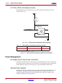
The diagram in Figure 1-30 shows the power supply architecture and maximum current
handling on each supply. The typical operating currents are significantly below the
maximum capable. The board is normally shipped with a 15W power supply, which
should be sufficient for most applications.
40
www.xilinx.com
SP601 Hardware User Guide
UG518 (v1.1) August 19, 2009
Power Management
The SP601 uses power solutions from LTC. An estimate of the current draw on the various
power supply rails is shown in Table 1-22.
X-Ref Target - Figure 1-30
5V
PWR
Jack
Monolithic Regulator
0.9V@3A max
Dual Switcher LTM4616
3. 3V@8A max
2. 5V@8A max
Dual Switcher LTM4616
1. 2V@8A max
1. 8V@8A max
Linear Regulator LT1763
3. 0V@500mA max
Buck-Boost Regulator LT1731
12V@1A max
UG518_30 _070809
Figure 1-30:
Table 1-22:
Estimated Current Draw
Rail (V)
Estimated Current (A)
FMC
12
1.0
3.3
3.0
LX16
Int/Aux
LX16
VCCO
DDR2
2.0
BPI/SPI
Flash
0.3
USB
CP2103
Clock Marvell Estimated
Socket EPHY
Totals
0.1
2.5
0.1
0.1
1.8
1.2
Power Supply
1.0
3.0
2.0
VTT 0.9
SP601 Hardware User Guide
UG518 (v1.1) August 19, 2009
1.0
www.xilinx.com
1.0
LTC
µModule
Comments
1.0
LT1731
12V, 3A
5.5
(1/2)
LTM4616
3.3V, 8A
1.1
(1/2)
LTM4616
2.5V, 8A
1.3
(1/2)
LTM4616
1.8V, 8A
5.0
(1/2)
LTM4616
1.2V, 8A
1.0
LTC3413
0.9V, 1.0A
41
Chapter 1: SP601 Evaluation Board
Configuration Options
The FPGA on the SP601 Evaluation Board can be configured by the following methods:
•
“3. SPI x4 Flash,” page 18
•
“4. Linear Flash BPI,” page 20
•
“JTAG Configuration,” page 42
For more information, refer to the Spartan-6 FPGA Configuration User Guide. [Ref 2]
Table 1-23:
Mode Pin Settings (M2 = 0)
Mode Pins (M1, M0)
Configuration Mode
00
Master Byte Peripheral Interface (BPI)
01
Master SPI x1, x2, or x4
10
Not implemented on SP601
11
Not implemented on SP601
JTAG Configuration
JTAG configuration is provided through onboard USB-to-JTAG configuration logic where
a computer host accesses the SP601 JTAG chain through a Type-A (computer host side) to
Type-Mini-B (SP601 side) USB cable.
The JTAG chain of the board is illustrated in Figure 1-31. JTAG configuration is allowable
at any time under any mode pin setting. JTAG initiated configuration takes priority over
the mode pin settings.
FMC bypass jumper J4 must be connected between pins 1-2 for JTAG access to the FPGA
on the basic SP601 board, as shown in Figure 1-31. When the VITA 57.1 FMC expansion
connector is populated with an expansion module that has a JTAG chain, then jumper J4
must be set to connect pins 2-3 in order to include the FMC expansion module's JTAG
chain in the main SP601 JTAG chain.
X-Ref Target - Figure 1-31
FPGA
USB Mini-B
Connector
J10
FMC LPC Expansion
TDI
TDO
TDI
U1
J1
J4
TDO
1
*Default jumper setting excludes FMC.
To include FMC, jumper pins 2-3.
UG518_31_070809
Figure 1-31:
42
www.xilinx.com
JTAG Chain
SP601 Hardware User Guide
UG518 (v1.1) August 19, 2009
Configuration Options
X-Ref Target - Figure 1-32
J4
1
FPGA_TD0
Bypass FMC LPC J1 = Jumper 1-2
2
JTAG_TD0
Include FMC LPC J1 = Jumper 2-3
3
FMC_TD0
H - 1x3
UG518_32_081909
Figure 1-32:
VITA 57.1 FMC JTAG Bypass Jumper
The JTAG chain can be used to program the FPGA and access the FPGA for hardware and
software debug.
The JTAG connector (USB Mini-B J10) allows a host computer to download bitstreams to
the FPGA using the iMPACT software tool, and also allows debug tools such as the
ChipScope™ Pro Analyzer tool or a software debugger to access the FPGA.
The iMPACT software tool can also program the SPI x4 flash or the BPI flash via the USB
J10 connection. iMPACT can download a temporary design to the FPGA through the
JTAG. This provides a connection within the FPGA from the FPGA's JTAG port to the
FPGA's SPI or BPI interface. Through the connection made by the temporary design in the
FPGA, iMPACT can indirectly program the SPI flash or BPI flash from the JTAG USB J10
connector.
SP601 Hardware User Guide
UG518 (v1.1) August 19, 2009
www.xilinx.com
43
Chapter 1: SP601 Evaluation Board
44
www.xilinx.com
SP601 Hardware User Guide
UG518 (v1.1) August 19, 2009
Appendix A
References
This section provides references to documentation supporting Spartan-6 FPGAs, tools,
and IP. For additional information, see
www.xilinx.com/support/documentation/index.htm.
Documents supporting the SP601 Evaluation Board:
1.
UG138, LogiCORE™ IP Tri-Mode Ethernet MAC v4.2 User Guide
2.
UG380, Spartan-6 FPGA Configuration User Guide
3.
UG381, Spartan-6 FPGA SelectIO Resources User Guide
4.
UG388, Spartan-6 FPGA Memory Controller User Guide
5.
DS614, Clock Generator (v3.01a) Data Sheet
6.
DS643, Multi-Port Memory Controller (MPMC) (v5.02a) Data Sheet
SP601 Hardware User Guide
UG518 (v1.1) August 19, 2009
www.xilinx.com
45
Appendix A: References
46
www.xilinx.com
SP601 Hardware User Guide
UG518 (v1.1) August 19, 2009
Appendix B
Default Jumper and Switch Settings
Table B-1 shows the default jumper and switch settings for the SP601.
Table B-1:
Default Jumper and Switch Settings
REFDES
SW1
SLIDE, POWER ON-OFF
SW2
DIP, 2-POLE, MODE
Default
OFF
1
M0
ON (1)
2
M1
OFF (0)
SW8
DIP, 4-POLE, GPIO
1
OFF
2
OFF
3
OFF
4
OFF
J4
SP601 Hardware User Guide
UG518 (v1.1) August 19, 2009
Type/Function
HDR_1X3, JTAG BYPASS
JUMP 1-2 (EXCLUDE FMC)
J14
HDR_1X2, SUSPEND
OPEN (0 = AWAKE)
J15
HDR_1X2, SPI SELECT
ON (U17 SPI MEM SELECTED)
www.xilinx.com
47
Appendix B: Default Jumper and Switch Settings
48
www.xilinx.com
SP601 Hardware User Guide
UG518 (v1.1) August 19, 2009
Appendix C
VITA 57.1 FMC Connections
Table C-1 shows the VITA 57.1 FMC LPC connections.
Table C-1:
VITA 57.1 FMC LPC Connections
J1 FMC
LPC Pin
Schematic Netname
U1 FPGA
Pin
J1 FMC
LPC Pin
Schematic Netname
U1 FPGA
Pin
C10
FMC_LA06_P
D12
D1
FMC_PWR_GOOD_FLASH_RST_B
B3
C11
FMC_LA06_N
C12
D8
FMC_LA01_CC_P
D11
C14
FMC_LA10_P
D8
D9
FMC_LA01_CC_N
C11
C15
FMC_LA10_N
C8
D11
FMC_LA05_P
B14
C18
FMC_LA14_P
B2
D12
FMC_LA05_N
A14
C19
FMC_LA14_N
A2
D14
FMC_LA09_P
G11
C22
FMC_LA18_CC_P
R10
D15
FMC_LA09_N
F10
C23
FMC_LA18_CC_N
T10
D17
FMC_LA13_P
B11
C26
FMC_LA27_P
R11
D18
FMC_LA13_N
A11
C27
FMC_LA27_N
T11
D20
FMC_LA17_CC_P
R8
C30
IIC_SCL_MAIN
P11
D21
FMC_LA17_CC_N
T8
C31
IIC_SDA_MAIN
N10
D23
FMC_LA23_P
N5
D24
FMC_LA23_N
P6
D26
FMC_LA26_P
U7
D27
FMC_LA26_N
V7
G2
FMC_CLK1_M2C_P
T9
H2
FMC_PRSNT_M2C_L
U13
G3
FMC_CLK1_M2C_N
V9
H4
FMC_CLK0_M2C_P
C10
G6
FMC_LA00_CC_P
D9
H5
FMC_CLK0_M2C_N
A10
G7
FMC_LA00_CC_N
C9
H7
FMC_LA02_P
C15
G9
FMC_LA03_P
C13
H8
FMC_LA02_N
A15
G10
FMC_LA03_N
A13
H10
FMC_LA04_P
B16
G12
FMC_LA08_P
F11
H11
FMC_LA04_N
A16
SP601 Hardware User Guide
UG518 (v1.1) August 19, 2009
www.xilinx.com
49
Appendix C: VITA 57.1 FMC Connections
Table C-1:
VITA 57.1 FMC LPC Connections (Cont’d)
J1 FMC
LPC Pin
Schematic Netname
U1 FPGA
Pin
J1 FMC
LPC Pin
Schematic Netname
U1 FPGA
Pin
G13
FMC_LA08_N
E11
H13
FMC_LA07_P
E7
G15
FMC_LA12_P
D6
H14
FMC_LA07_N
E8
G16
FMC_LA12_N
C6
H16
FMC_LA11_P
B12
G18
FMC_LA16_P
C7
H17
FMC_LA11_N
A12
G19
FMC_LA16_N
A7
H19
FMC_LA15_P
G9
G21
FMC_LA20_P
N7
H20
FMC_LA15_N
F9
G22
FMC_LA20_N
P8
H22
FMC_LA19_P
N6
G24
FMC_LA22_P
R7
H23
FMC_LA19_N
P7
G25
FMC_LA22_N
T7
H25
FMC_LA21_P
T4
G27
FMC_LA25_P
M11
H26
FMC_LA21_N
V4
G28
FMC_LA25_N
N11
H28
FMC_LA24_P
U8
G30
FMC_LA29_P
M8
H29
FMC_LA24_N
V8
G31
FMC_LA29_N
N8
H31
FMC_LA28_P
U11
G33
FMC_LA31_P
T6
H32
FMC_LA28_N
V11
G34
FMC_LA31_N
V6
H34
FMC_LA30_P
T12
G36
FMC_LA33_P
M10
H35
FMC_LA30_N
V12
G37
FMC_LA33_N
N9
H37
FMC_LA32_P
U15
H38
FMC_LA32_N
V15
50
www.xilinx.com
SP601 Hardware User Guide
UG518 (v1.1) August 19, 2009
Appendix D
SP601 Master UCF
The UCF template is provided for designs that target the SP601. Net names provided in the
constraints below correlate with net names on the SP601 rev. C schematic. On identifying
the appropriate pins, the net names below should be replaced with net names in the user
RTL. See the Constraints Guide for more information.
NET
NET
NET
NET
NET
NET
NET
NET
NET
NET
NET
NET
NET
NET
NET
NET
NET
NET
NET
NET
NET
NET
NET
NET
NET
NET
NET
NET
NET
NET
NET
NET
NET
NET
NET
NET
NET
NET
NET
SP601 Hardware User Guide
UG518 (v1.1) August 19, 2009
"CPU_RESET"
"DDR2_A0"
"DDR2_A1"
"DDR2_A2"
"DDR2_A3"
"DDR2_A4"
"DDR2_A5"
"DDR2_A6"
"DDR2_A7"
"DDR2_A8"
"DDR2_A9"
"DDR2_A10"
"DDR2_A11"
"DDR2_A12"
"DDR2_BA0"
"DDR2_BA1"
"DDR2_BA2"
"DDR2_CAS_B"
"DDR2_CKE"
"DDR2_CLK_N"
"DDR2_CLK_P"
"DDR2_DQ0"
"DDR2_DQ1"
"DDR2_DQ2"
"DDR2_DQ3"
"DDR2_DQ4"
"DDR2_DQ5"
"DDR2_DQ6"
"DDR2_DQ7"
"DDR2_DQ8"
"DDR2_DQ9"
"DDR2_DQ10"
"DDR2_DQ11"
"DDR2_DQ12"
"DDR2_DQ13"
"DDR2_DQ14"
"DDR2_DQ15"
"DDR2_LDM"
"DDR2_LDQS_N"
LOC
LOC
LOC
LOC
LOC
LOC
LOC
LOC
LOC
LOC
LOC
LOC
LOC
LOC
LOC
LOC
LOC
LOC
LOC
LOC
LOC
LOC
LOC
LOC
LOC
LOC
LOC
LOC
LOC
LOC
LOC
LOC
LOC
LOC
LOC
LOC
LOC
LOC
LOC
www.xilinx.com
=
=
=
=
=
=
=
=
=
=
=
=
=
=
=
=
=
=
=
=
=
=
=
=
=
=
=
=
=
=
=
=
=
=
=
=
=
=
=
"N4";
"J7";
"J6";
"H5";
"L7";
"F3";
"H4";
"H3";
"H6";
"D2";
"D1";
"F4";
"D3";
"G6";
"F2";
"F1";
"E1";
"K5";
"H7";
"G1";
"G3";
"L2";
"L1";
"K2";
"K1";
"H2";
"H1";
"J3";
"J1";
"M3";
"M1";
"N2";
"N1";
"T2";
"T1";
"U2";
"U1";
"K3";
"L3";
51
Appendix D: SP601 Master UCF
NET
NET
NET
NET
NET
NET
NET
NET
NET
NET
NET
NET
NET
NET
NET
NET
NET
NET
NET
NET
NET
NET
NET
NET
NET
NET
NET
NET
NET
NET
NET
NET
NET
NET
NET
NET
NET
NET
NET
NET
NET
NET
NET
NET
NET
NET
NET
NET
NET
NET
NET
NET
NET
NET
NET
NET
NET
NET
NET
52
"DDR2_LDQS_P"
"DDR2_ODT"
"DDR2_RAS_B"
"DDR2_UDM"
"DDR2_UDQS_N"
"DDR2_UDQS_P"
"DDR2_WE_B"
"FLASH_A0"
"FLASH_A1"
"FLASH_A2"
"FLASH_A3"
"FLASH_A4"
"FLASH_A5"
"FLASH_A6"
"FLASH_A7"
"FLASH_A8"
"FLASH_A9"
"FLASH_A10"
"FLASH_A11"
"FLASH_A12"
"FLASH_A13"
"FLASH_A14"
"FLASH_A15"
"FLASH_A16"
"FLASH_A17"
"FLASH_A18"
"FLASH_A19"
"FLASH_A20"
"FLASH_A21"
"FLASH_A22"
"FLASH_A23"
"FLASH_A24"
"FLASH_CE_B"
"FLASH_D3"
"FLASH_D4"
"FLASH_D5"
"FLASH_D6"
"FLASH_D7"
"FLASH_OE_B"
"FLASH_WE_B"
"FMC_CLK0_M2C_N"
"FMC_CLK0_M2C_P"
"FMC_CLK1_M2C_N"
"FMC_CLK1_M2C_P"
"FMC_LA00_CC_N"
"FMC_LA00_CC_P"
"FMC_LA01_CC_N"
"FMC_LA01_CC_P"
"FMC_LA02_N"
"FMC_LA02_P"
"FMC_LA03_N"
"FMC_LA03_P"
"FMC_LA04_N"
"FMC_LA04_P"
"FMC_LA05_N"
"FMC_LA05_P"
"FMC_LA06_N"
"FMC_LA06_P"
"FMC_LA07_N"
www.xilinx.com
LOC
LOC
LOC
LOC
LOC
LOC
LOC
LOC
LOC
LOC
LOC
LOC
LOC
LOC
LOC
LOC
LOC
LOC
LOC
LOC
LOC
LOC
LOC
LOC
LOC
LOC
LOC
LOC
LOC
LOC
LOC
LOC
LOC
LOC
LOC
LOC
LOC
LOC
LOC
LOC
LOC
LOC
LOC
LOC
LOC
LOC
LOC
LOC
LOC
LOC
LOC
LOC
LOC
LOC
LOC
LOC
LOC
LOC
LOC
=
=
=
=
=
=
=
=
=
=
=
=
=
=
=
=
=
=
=
=
=
=
=
=
=
=
=
=
=
=
=
=
=
=
=
=
=
=
=
=
=
=
=
=
=
=
=
=
=
=
=
=
=
=
=
=
=
=
=
"L4";
"K6";
"L5";
"K4";
"P1";
"P2";
"E3";
"K18";
"K17";
"J18";
"J16";
"G18";
"G16";
"H16";
"H15";
"H14";
"H13";
"F18";
"F17";
"K13";
"K12";
"E18";
"E16";
"G13";
"H12";
"D18";
"D17";
"G14";
"F14";
"C18";
"C17";
"F16";
"L17";
"U5";
"V5";
"R3";
"T3";
"R5";
"L18";
"M16";
"A10";
"C10";
"V9";
"T9";
"C9";
"D9";
"C11";
"D11";
"A15";
"C15";
"A13";
"C13";
"A16";
"B16";
"A14";
"B14";
"C12";
"D12";
"E8";
SP601 Hardware User Guide
UG518 (v1.1) August 19, 2009
NET
NET
NET
NET
NET
NET
NET
NET
NET
NET
NET
NET
NET
NET
NET
NET
NET
NET
NET
NET
NET
NET
NET
NET
NET
NET
NET
NET
NET
NET
NET
NET
NET
NET
NET
NET
NET
NET
NET
NET
NET
NET
NET
NET
NET
NET
NET
NET
NET
NET
NET
NET
NET
NET
NET
NET
NET
NET
NET
SP601 Hardware User Guide
UG518 (v1.1) August 19, 2009
"FMC_LA07_P"
"FMC_LA08_N"
"FMC_LA08_P"
"FMC_LA09_N"
"FMC_LA09_P"
"FMC_LA10_N"
"FMC_LA10_P"
"FMC_LA11_N"
"FMC_LA11_P"
"FMC_LA12_N"
"FMC_LA12_P"
"FMC_LA13_N"
"FMC_LA13_P"
"FMC_LA14_N"
"FMC_LA14_P"
"FMC_LA15_N"
"FMC_LA15_P"
"FMC_LA16_N"
"FMC_LA16_P"
"FMC_LA17_CC_N"
"FMC_LA17_CC_P"
"FMC_LA18_CC_N"
"FMC_LA18_CC_P"
"FMC_LA19_N"
"FMC_LA19_P"
"FMC_LA20_N"
"FMC_LA20_P"
"FMC_LA21_N"
"FMC_LA21_P"
"FMC_LA22_N"
"FMC_LA22_P"
"FMC_LA23_N"
"FMC_LA23_P"
"FMC_LA24_N"
"FMC_LA24_P"
"FMC_LA25_N"
"FMC_LA25_P"
"FMC_LA26_N"
"FMC_LA26_P"
"FMC_LA27_N"
"FMC_LA27_P"
"FMC_LA28_N"
"FMC_LA28_P"
"FMC_LA29_N"
"FMC_LA29_P"
"FMC_LA30_N"
"FMC_LA30_P"
"FMC_LA31_N"
"FMC_LA31_P"
"FMC_LA32_N"
"FMC_LA32_P"
"FMC_LA33_N"
"FMC_LA33_P"
"FMC_PRSNT_M2C_L"
"FMC_PWR_GOOD_FLASH_RST_B"
"FPGA_AWAKE"
"FPGA_CCLK"
"FPGA_CMP_CLK"
"FPGA_CMP_CS_B"
www.xilinx.com
LOC
LOC
LOC
LOC
LOC
LOC
LOC
LOC
LOC
LOC
LOC
LOC
LOC
LOC
LOC
LOC
LOC
LOC
LOC
LOC
LOC
LOC
LOC
LOC
LOC
LOC
LOC
LOC
LOC
LOC
LOC
LOC
LOC
LOC
LOC
LOC
LOC
LOC
LOC
LOC
LOC
LOC
LOC
LOC
LOC
LOC
LOC
LOC
LOC
LOC
LOC
LOC
LOC
LOC
LOC
LOC
LOC
LOC
LOC
=
=
=
=
=
=
=
=
=
=
=
=
=
=
=
=
=
=
=
=
=
=
=
=
=
=
=
=
=
=
=
=
=
=
=
=
=
=
=
=
=
=
=
=
=
=
=
=
=
=
=
=
=
=
=
=
=
=
=
"E7";
"E11";
"F11";
"F10";
"G11";
"C8";
"D8";
"A12";
"B12";
"C6";
"D6";
"A11";
"B11";
"A2";
"B2";
"F9";
"G9";
"A7";
"C7";
"T8";
"R8";
"T10";
"R10";
"P7";
"N6";
"P8";
"N7";
"V4";
"T4";
"T7";
"R7";
"P6";
"N5";
"V8";
"U8";
"N11";
"M11";
"V7";
"U7";
"T11";
"R11";
"V11";
"U11";
"N8";
"M8";
"V12";
"T12";
"V6";
"T6";
"V15";
"U15";
"N9";
"M10";
"U13";
"B3";
"P15";
"R15";
"U16";
"P13";
53
Appendix D: SP601 Master UCF
NET
NET
NET
NET
NET
NET
NET
NET
NET
NET
NET
NET
NET
NET
NET
NET
NET
NET
NET
NET
NET
NET
NET
NET
NET
NET
NET
NET
NET
NET
NET
NET
NET
NET
NET
NET
NET
NET
NET
NET
NET
NET
NET
NET
NET
NET
NET
NET
NET
NET
NET
NET
NET
NET
NET
NET
NET
NET
NET
54
"FPGA_CMP_MOSI"
"FPGA_D0_DIN_MISO_MISO1"
"FPGA_D1_MISO2"
"FPGA_D2_MISO3"
"FPGA_DONE"
"FPGA_HSWAPEN"
"FPGA_INIT_B"
"FPGA_M0_CMP_MISO"
"FPGA_M1"
"FPGA_MOSI_CSI_B_MISO0"
"FPGA_ONCHIP_TERM1"
"FPGA_ONCHIP_TERM2"
"FPGA_PROG_B"
"FPGA_SUSPEND"
"FPGA_TCK_BUF"
"FPGA_TDI_BUF"
"FPGA_TDO"
"FPGA_TMS_BUF"
"FPGA_VTEMP"
"GPIO_BUTTON0"
"GPIO_BUTTON1"
"GPIO_BUTTON2"
"GPIO_BUTTON3"
"GPIO_HDR0"
"GPIO_HDR1"
"GPIO_HDR2"
"GPIO_HDR3"
"GPIO_HDR4"
"GPIO_HDR5"
"GPIO_HDR6"
"GPIO_HDR7"
"GPIO_LED_0"
"GPIO_LED_1"
"GPIO_LED_2"
"GPIO_LED_3"
"GPIO_SWITCH_0"
"GPIO_SWITCH_1"
"GPIO_SWITCH_2"
"GPIO_SWITCH_3"
"IIC_SCL_MAIN"
"IIC_SDA_MAIN"
"PHY_COL"
"PHY_CRS"
"PHY_INT"
"PHY_MDC"
"PHY_MDIO"
"PHY_RESET"
"PHY_RXCLK"
"PHY_RXCTL_RXDV"
"PHY_RXD0"
"PHY_RXD1"
"PHY_RXD2"
"PHY_RXD3"
"PHY_RXD4"
"PHY_RXD5"
"PHY_RXD6"
"PHY_RXD7"
"PHY_RXER"
"PHY_TXCLK"
www.xilinx.com
LOC
LOC
LOC
LOC
LOC
LOC
LOC
LOC
LOC
LOC
LOC
LOC
LOC
LOC
LOC
LOC
LOC
LOC
LOC
LOC
LOC
LOC
LOC
LOC
LOC
LOC
LOC
LOC
LOC
LOC
LOC
LOC
LOC
LOC
LOC
LOC
LOC
LOC
LOC
LOC
LOC
LOC
LOC
LOC
LOC
LOC
LOC
LOC
LOC
LOC
LOC
LOC
LOC
LOC
LOC
LOC
LOC
LOC
LOC
=
=
=
=
=
=
=
=
=
=
=
=
=
=
=
=
=
=
=
=
=
=
=
=
=
=
=
=
=
=
=
=
=
=
=
=
=
=
=
=
=
=
=
=
=
=
=
=
=
=
=
=
=
=
=
=
=
=
=
"V16";
"R13";
"T14";
"V14";
"V17";
"D4";
"U3";
"T15";
"N12";
"T13";
"L6";
"C2";
"V2";
"R16";
"A17";
"D15";
"D16";
"B18";
"P3";
"P4";
"F6";
"E4";
"F5";
"N17";
"M18";
"A3";
"L15";
"F15";
"B4";
"F13";
"P12";
"E13";
"C14";
"C4";
"A4";
"D14";
"E12";
"F12";
"V13";
"P11";
"N10";
"L14";
"M13";
"J13";
"N14";
"P16";
"L13";
"L16";
"N18";
"M14";
"U18";
"U17";
"T18";
"T17";
"N16";
"N15";
"P18";
"P17";
"B9";
SP601 Hardware User Guide
UG518 (v1.1) August 19, 2009
NET
NET
NET
NET
NET
NET
NET
NET
NET
NET
NET
NET
NET
NET
NET
NET
NET
NET
NET
NET
NET
SP601 Hardware User Guide
UG518 (v1.1) August 19, 2009
"PHY_TXCTL_TXEN"
"PHY_TXC_GTXCLK"
"PHY_TXD0"
"PHY_TXD1"
"PHY_TXD2"
"PHY_TXD3"
"PHY_TXD4"
"PHY_TXD5"
"PHY_TXD6"
"PHY_TXD7"
"PHY_TXER"
"SMACLK_N"
"SMACLK_P"
"SPI_CS_B"
"SYSCLK_N"
"SYSCLK_P"
"USB_1_CTS"
"USB_1_RTS"
"USB_1_RX"
"USB_1_TX"
"USER_CLOCK"
www.xilinx.com
LOC
LOC
LOC
LOC
LOC
LOC
LOC
LOC
LOC
LOC
LOC
LOC
LOC
LOC
LOC
LOC
LOC
LOC
LOC
LOC
LOC
=
=
=
=
=
=
=
=
=
=
=
=
=
=
=
=
=
=
=
=
=
"B8";
"A9";
"F8";
"G8";
"A6";
"B6";
"E6";
"F7";
"A5";
"C5";
"A8";
"H18";
"H17";
"V3";
"K16";
"K15";
"U10";
"T5";
"L12";
"K14";
"V10";
55