1
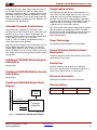
I
R
<
B
L
ChipScope PLBv46 IBA (Bus Analyzer) (v1.00a)
DS619 (v1.0) September 17, 2007
Product Specification
Introduction
LogiCORE™ Facts
The ChipScope™ PLB IBA core is a specialized Bus
Analyzer core designed to debug embedded systems that
contain the IBM CoreConnect™ Processor Local Bus (PLB)
version 4.6. The ChipScope PLB46 IBA core in EDK is
based on a Tcl script that generates an HDL wrapper to the
PLB IBA and calls the ChipScope Core Generator to
generate the netlist based on user parameters.
Core Specifics
Supported Device
Family
Virtex-E, Virtex, Spartan™-3A DSP,
Spartan-3AN, Spartan-3A, Spartan-3E,
Spartan-3, Spartan-IIE, Spartan-II, Virtex-5
LX, Virtex-5 LXT Virtex-5 SXT, Virtex-4 FX,
Virtex-4 LX, Virtex-4 SX, Virtex-II Pro,
Virtex-II, Virtex-II Pro, Virtex-4
Version of Core
chipscope_plb46_iba
V1.00a
Resources Used
Features
Min
The ChipScope PLBv46 IBA is a soft IP core designed for
Xilinx® FPGAs and contains the following features:
Max
Slices
LUTs
•
Probes the master, slave, arbiter, and error status
signals of the PLBv46 bus
•
Probes the PLBv46 OR'ed slave signals
•
Automatically adjusts ports to the PLBv46 bus width
•
Documentation
Product Specification
Separates master, slave, and error status signals into
independent match units which can be enabled or
disabled by a design parameter
Design File
Formats
VHDL/EDIF
•
Constraints File
N/A
Allows independent enabling or disabling of probed
master, slave, and error status signals for data capture
Verification
N/A
•
Supports trigger port customization by a design
parameter
Instantiation
Template
N/A
•
Supports match unit type customization for each trigger
port by a design parameter
•
Supports sample depths from 1024-131,072 on
Virtex™-5 Devices selectable by a design parameter
Xilinx
Implementation
Tools
ISE™ 9.2i or later
•
Can probe as few as 1 signals and as many as 1115
signals on a Virtex-5 device
Verification
ChipScope Pro 9.2i or later
•
Simulation
Not supported in simulation
Provides a separate input bus to allow a user-defined
input debug port
Synthesis
XST
•
Supports a trigger output indicator pin that can be sent
off chip or to other cores
FFs
Block RAMs
Provided with Core
Reference Designs None
Design Tool Requirements
Support
Provided by Xilinx, Inc.
© 2007 Xilinx, Inc. All rights reserved. All Xilinx trademarks, registered trademarks, patents, and disclaimers are as listed at http://www.xilinx.com/legal.htm.
PowerPC is a trademark of IBM, Inc. All other trademarks are the property of their respective owners. All specifications are subject to change without notice.
DS619 (v1.0) September 17, 2007
Product Specification
www.xilinx.com
1
R
ChipScope PLBv46 IBA (Bus Analyzer) (v1.00a)
ChipScope PLB46 IBA I/O Signals
Table 1: IBA_PLBv46 Pin Descriptions
Port
MU
Signal Name
Interface
I/O
Description
P1
CONTROL
ICON
I/O
Icon control bus IO
P2
PLB_Clk
System
I
System Clock
iba_trigin_in
GENERIC
I
Generic Trigger Inputs
iba_trig_out
GENERIC
O
IBA Trigger Output
P3
MU_1C
P4
Reset & Error Status
P5
MU_1A
PLB_Rst
System
I
Registered reset output from arbitration
logic
P6
MU_1A
Bus_Error_Det
System
I
Bus Error Interrupt
P7
MU_1A
PLB_lockErr
Slave
I
PLB lock error indicator
P8
MU_1B
PLB_MRdErr[0:
C_PLBV46_NUM_MASTERS-1]
Master
I
PLB Master slave read error indicator
P9
MU_1B
PLB_MWrErr[0:
C_PLBV46_NUM_MASTERS-1]
Master
I
PLB Master slave write error indicator
P10
MU_1B
PLB_MIRQ[0:
C_PLBV46_NUM_MASTERS-1]
Master
I
Master interrupt request. For each master,
indicates when a slave has encountered an
event that is significant to the master
P11
MU_1B
PLB_MTimeout[0:
C_PLBV46_NUM_MASTERS-1]
Master
I
PLB address-phase timeout indicator
Common Signals
P12
MU_2A
PLB_PAValid
Slave
I
PLB primary address valid indicator
P13
MU_2A
PLB_SAValid
Slave
I
PLB secondary address
P14
MU_2A
PLB_busLock
Slave
I
PLB BusLock
P15
MU_2A
PLB_abort
Slave
I
PLB abort bus request indicator
P16
MU_2A
PLB_Swait
Simulation
I
Output of Sl_wait OR gate
P17
MU_2A
PLB_SaddrAck
Simulation
I
Output of Sl_addrAck OR gate
P18
MU_2A
PLB_Srearbitrate
Simulation
I
Output of Sl_rearbitrate OR gate
P19
MU_2A
PLB_RNW
Slave
I
PLB read not write
P20
MU_2A
PLB_SwrDAck
Simulation
I
Output of Sl_wrDAck OR gate
P21
MU_2A
PLB_SwrComp
Simulation
I
Output of Sl_wrComp OR gate
P22
MU_2A
PLB_SwrBTerm
Simulation
I
Output of Sl_wrBTerm OR gate
P23
MU_2A
PLB_wrBurst
Slave
I
PLB burst write transfer indicator
P24
MU_2A
PLB_SrdDAck
Simulation
I
Output of Sl_rdDAck OR gate
P25
MU_2A
PLB_SrdComp
Simulation
I
Output of Sl_rdComp OR gate
P26
MU_2A
PLB_SrdBTerm
Simulation
I
Output of Sl_rdBTerm OR gate
P27
MU_2A
PLB_rdBurst
Slave
I
PLB burst read transfer indicator
P28
MU_2B
PLB_size[0:3]
Slave
I
PLB Transfer size
P29
MU_2B
PLB_type[0:2]
Slave
I
PLB Transfer type
P30
MU_2B
PLB_MSize[0:1]
Slave
I
PLB data bus port width indicator.
P31
MU_2B
PLB_Ssize[0:1]
Simulation
I
Output of slave Sl_SSize OR gate
P32
MU_2B
PLB_masterID[0:
C_PLBV46_MID_WIDTH-1]
Slave
I
PLB current master identifier
P33
MU_2B
PLB_BE[0: C_PLBV46_DWIDTH/8-1]
Slave
I
PLB byte enables
DS619 (v1.0) September 17, 2007
Product Specification
www.xilinx.com
2
R
ChipScope PLBv46 IBA (Bus Analyzer) (v1.00a)
Table 1: IBA_PLBv46 Pin Descriptions (Continued)
Port
P34
MU
MU_2C
Signal Name
Interface
PLB_TAttribute[0:15]
Slave
I/O
Description
I
PLB Transfer Attribute
Address
P35
MU_3A
PLB_ABus[0:31]
Slave
I
PLB address bus, lower 32 bits
P36
MU_3B
PLB_UABus[0:31]
Slave
I
PLB address bus, upper 32 bits
Data
P37
MU_4
PLB_wrDBus[0: C_PLBV46_DWIDTH-1]
Slave
I
PLB write data bus
P38
MU_5
PLB_SrdDBus[0:
C_PLBV46_DWIDTH-1]
Sim
I
Output of SL_rdDBus OR gate
Slave
P39
MU_6A
PLB_rdPrim[0:
C_PLBV46_NUM_SLAVES-1]
Slave
I
PLB secondary to primary read request
indicator
P40
MU_6A
PLB_wrPrim[0:
C_PLBV46_NUM_SLAVES-1]
Slave
I
PLB secondary to primary write request
indicator
P41
MU_6A
Sl_AddrAck[0:
C_PLBV46_NUM_SLAVES-1]
Slave
I
Slave Address acknowledge
P42
MU_6A
Sl_Rearbitrate[0:
C_PLBV46_NUM_SLAVES-1]
Slave
I
Slave bus re-arbitrate indicator
P43
MU_6A
Sl_wait[0: C_PLBV46_NUM_SLAVES-1]
Slave
I
Slave wait indicator
P44
MU_6A
Sl_rdBTerm[0:
C_PLBV46_NUM_SLAVES -1]
Slave
I
Slave terminate read burst indicator
P45
MU_6A
Sl_rdComp[0:
C_PLBV46_NUM_SLAVES -1]
Slave
I
Slave read transfer complete indicator
P46
MU_6A
Sl_rdDAck[0:
C_PLBV46_NUM_SLAVES-1]
Slave
I
Slave read data acknowledge
P47
MU_6A
Sl_wrBTerm[0:
C_PLBV46_NUM_SLAVES -1]
Slave
I
Slave terminate write burst indicator
P48
MU_6A
Sl_wrComp[0:
C_PLBV46_NUM_SLAVES -1]
Slave
I
Slave write transfer complete indicator
P49
MU_6A
Sl_wrDAck[0:
C_PLBV46_NUM_SLAVES-1]
Slave
I
Slave write data acknowledge
P50
MU_6B
Sl_rdWdAddr[0:
C_PLBV46_NUM_SLAVES*4-1]
Slave
I
Slave read word address
P51
MU_6B
Sl_SSize[0:
C_PLBV46_NUM_SLAVES*2-1]
Slave
I
Slave data bus port size indicator
P52
MU_7
Sl_MBusy[0: C_PLBV46_NUM_SLAVES
*C_PLBV46_NUM_MASTERS-1]
Slave
I
Slave busy indicator
P53
MU_8
Sl_MRdErr[0:
C_PLBV46_NUM_SLAVES
*C_PLBV46_NUM_MASTERS-1]
Slave
I
Slave read error indicator
P54
MU_9
Sl_MWrErr[0:
C_PLBV46_NUM_SLAVES
*C_PLBV46_NUM_MASTERS-1]
Slave
I
Slave write error indicator
PLB Arbitration Signals
P55
MU_10
M_request[0:
C_PLBV46_NUM_MASTERS-1]
Master
I
Master bus request
P56
MU_10
M_priority[0:
C_PLBV46_NUM_MASTERS*2-1]
Master
I
Master bus request priority
P57
MU_10
M_busLock[0:
C_PLBV46_NUM_MASTERS-1]
Master
I
Master Bus Lock
DS619 (v1.0) September 17, 2007
Product Specification
www.xilinx.com
3
R
ChipScope PLBv46 IBA (Bus Analyzer) (v1.00a)
Table 1: IBA_PLBv46 Pin Descriptions (Continued)
Port
MU
Signal Name
Interface
I/O
Description
P58
MU_10
M_abort[0:
C_PLBV46_NUM_MASTERS-1]
Master
I
Master abort bus request indicator
P59
MU_10
PLB_rdPendPri[0:1]
Master
I
PLB pending read request priority
P60
MU_10
PLB_wrPendPri[0:1]
Master
I
PLB pending write request priority
P61
MU_10
PLB_rdPendReq
Master /Slave I
PLB pending bus read request indicator
P62
MU_10
PLB_wrPendReq
Master /Slave I
PLB pending bus write request indicator
P63
MU_10
PLB_reqPri[0:1]
Master /Slave I
PLB current request priority
PLB Master Signals
P64
MU_11
M_lockErr[0:
C_PLBV46_NUM_MASTERS-1]
Master
I
Master lock error indicator
P65
MU_11
M_rdBurst[0:
C_PLBV46_NUM_MASTERS-1]
Master
I
Master read burst indicator
P66
MU_11
M_wrBurst[0:
C_PLBV46_NUM_MASTERS-1]
Master
I
Master write burst indicator
P67
MU_11
M_RNW[0:
C_PLBV46_NUM_MASTERS-1]
Master
I
Master read not write
P68
MU_11
PLB_MBusy[0:
C_PLBV46_NUM_MASTERS-1]
Master
I
PLB Master slave busy indicator
P69
MU_11
PLB_MAddrAck[0:
C_PLBV46_NUM_MASTERS-1]
Master
I
PLB Master Address acknowledge
P70
MU_11
PLB_MRdBTerm[0:
C_PLBV46_NUM_MASTERS-1]
Master
I
PLB Master terminate read burst indicator
P71
MU_11
PLB_MRdDAck[0:
C_PLBV46_NUM_MASTERS-1]
Master
I
PLB Master read data acknowledge
P72
MU_11
PLB_MRearbitrate[0:
C_PLBV46_NUM_MASTERS-1]
Master
I
PLB Master bus re-arbitrate indicator
P73
MU_11
PLB_MWrBTerm[0:
C_PLBV46_NUM_MASTERS-1]
Master
I
PLB Master terminate write burst indicator
P74
MU_11
PLB_MWrDAck[0:
C_PLBV46_NUM_MASTERS-1]
Master
I
PLB Master write data acknowledge
P75
MU_12
M_mSize[0:
C_PLBV46_NUM_MASTERS*2-1]
Master
I
Master data bus port width
P76
MU_12
M_size[0:
C_PLBV46_NUM_MASTERS*4-1]
Master
I
Master transfer size
P77
MU_12
PLB_MSSize[0:
C_PLBV46_NUM_MASTERS*2-1]
Master
I
PLB Master slave data bus width indicator
P78
MU_12
M_type[0:
C_PLBV46_NUM_MASTERS*3-1]
Master
I
Master transfer type
P79
MU_13
M_BE[0: C_PLBV46_NUM_MASTERS*
C_PLBV46_DWIDTH/8-1]
Master
I
Master byte enables
The IBA_PLBv46 ports listed in Table 1connect to the
PLBv46 bus. The core divides related ports into 13 match
unit groups (MUs) as shown in the second column of the
table. Each match unit group can connect to a trigger port of
the IBA. Certain match unit groups, such as MU_1, are
further subdivided to allow more fine control of the signals
attached to a trigger port. For example, PLB_Rst is part of
MU_1A and PLB_MRdErr is part of MU_1B but both will be
combined into MU_1 when enabled.
DS619 (v1.0) September 17, 2007
Product Specification
Every match unit label has a match type and match counter
width parameter. The match unit type describes the type of
compare operation that can be done with the match unit.
The valid values for this type are defined for each match
unit. For instance C_MU_1_TYPE only supports basic and
basic with edges because multiple signals make up this
match unit bus; whereas for C_MU_3_TYPE, all compare
options are available because this match unit has only one
connected signal bus type. The match counter width allows
www.xilinx.com
4
R
ChipScope PLBv46 IBA (Bus Analyzer) (v1.00a)
enabled and defined with unique C_MU_xx_TYPE pattern
match units.
a user to look for multiple occurrences of the match event.
This counter width is controllable through the
C_MU_xx_CNT_W parameter (xx is a place holder for
1-13). When this parameter is set to 0 only 1 occurrence is
counted, otherwise the match event count is limited by the
width of this parameter.
The 6a and 6b match units are used for the slave side
interface. This match unit holds all the control and status
ports of all the slaves on the PLB. Similarly, match units 11,
12 and 13 have all the control and status of all the masters.
The number of match units to use is defined by the
C_MU_xx_NUM parameter. By default if a match unit does
not have the C_MU_xx_NUM parameter then only one
match unit is used for the match group. If the
C_MU_xx_NUM parameter is defined, then one or two
match units are available for this match group. What this
enables is looking at sequences of this particular match
group. For instance in match group 2 you may want a trigger
sequence to first look at PLB_PAValid=1 followed by a rising
edge on PLB_SaddrAck. For this specific trigger the first
match unit is set to look for PLB_PAValid=1 and the second
is set for PLB_SaddrAck=R.
Note: When these match units are enabled, all slaves or masters
are enabled. You cannot individually enable a particular master.
The match units 7, 8, and 9 are slave side signals for BUSY,
READ, and WRITE error controls going to the master.
These units are broken out individually because this bus
has one signal for each master on each slave.
Consequently, you can have up to 256 signals on each one
of these match units (if PLB goes to a 16 slave, 16 master
solution).
The arbiter status signals can be monitored using match
unit 10. The signals probed by this match unit can help
identify the order of the PLB master transactions that are
being sorted on the bus.
The first match unit is labeled 1a and 1b. The 1a group of
signals makes up the reset and error flag signals. The 1b
group contains master related error signals. The generator
allows adding 1a, 1b or both of these groups to the core via
the generic parameters C_USE_MU_1A, and
C_USE_MU_1B respectively.
ChipScope PLB46 IBA Parameters
To create a ChipScope PLB46 IBA uniquely tailored for your
system and to optimize performance, specific features can
be parameterized on the PLB IBA. Table 2 describes the
features that can be parameterized.
The second match unit has labels 2a, 2b, and 2c. The 2a
signals contain 16 of the primitive ports which provide
essential PLB bus transaction information. The 2b signals
contain buses that identify widths and master information of
the active transaction. The 2c label is used for the
transaction attribute bus. The three subdivided match unit
groups can be all or individually enabled using the
parameters C_USE_MU_2A, C_USE_MU_2B, and
C_USE_MU_2C.
The ChipScope PLB IBA peripheral supports multiple
trigger units that connect to the PLB Control bus, Address
bus, Data bus, lumped Slave or Master busses. Each one of
these trigger units can be enabled and parameterized
independently. Table 2 lists all the parameters used in
selecting the trigger port connections. These parameters
define what signals are connected to the trigger ports, the
match unit type, and if the signals are stored in the sample
buffer.
The third, fourth, and fifth match units are used for the
address, data write, and data read buses respectively. Each
bus has a dedicated match unit so it can be individually
Table 2: IBA_PLBv46 Design Parameters
Generic
Feature/Description
Parameter Name
Allowable Values
Virtex5
VHDL
Type
G1
Target Family
C_FAMILY
G2
Device
C_DEVICE
String
G3
Device Package
C_PACKAGE
String
G4
Device speed grade
C_SPEEDGRADE
String
G5
Number of PLB Masters
C_PLBV46_NUM_MASTERS
1-8
2
Integer
G6
Number of PLB Slaves
C_PLBV46_NUM_SLAVES
1-8
1
Integer
G7
Number of bits required to encode the
number of PLB Masters
C_PLBV46_MID_WIDTH
1-5
2
Integer
DS619 (v1.0) September 17, 2007
Product Specification
Spartan3,
Spartan3E,
Spartan3A,
Spartan3ADSP,
Spartan3AN,
Virtex, VirtexE,
Virtex4, Virtex5
Default
Value
String
www.xilinx.com
5
R
ChipScope PLBv46 IBA (Bus Analyzer) (v1.00a)
Table 2: IBA_PLBv46 Design Parameters (Continued)
Generic
Feature/Description
Parameter Name
Allowable Values
Default
Value
VHDL
Type
G8
PLB Address Bus Width
C_PLBV46_AWIDTH
32
32
Integer
G9
PLB Data Bus Width
C_PLBV46_DWIDTH
32,64,128
64
Integer
IBA Storage Options and Trig Out
G10
Number of data samples captured for every C_NUM_DATA_SAMPLES
trigger match. Note that the range of
acceptable values depends on the
C_FAMILY value.
512, 1024, 2048,
1024
4096, 8192, 16384,
32768, 65536,
131072
Integer
G11
Number of sequencer levels. If 0 then no
sequencer is used.
0-16
0
Integer
G12
1=Enable data store qualification (filtering) C_ENABLE_STORAGE_
QUALIFICATION
0=Disable
0,1
1
Integer
G13
Enable Trigger Out
1,0
0
Integer
C_MAX_SEQUENCER_
LEVELS
C_ENABLE_TRIGGER_OUT
Trigger In, PLB Reset, and PLB Error Status
G14
Use system reset and error status signals
C_USE_MU_1A_RST_ERR_
STAT
1,0
1
Integer
G15
Use master error status signals
C_USE_MU_1B_MSTR_RST_
ERR_STAT
1,0
0
Integer
G16
Use iba_trig_in
C_USE_MU_1C_TRIG_IN
1,0
0
Integer
G17
Trigger in width, 0=disable
C_MU_1_TRIG_IN_WIDTH
0-189
0
Integer
G18
0=basic, 1=basic w/ edges
C_MU_1_TYPE_TRIG_RST_
ERR_STAT
0,1
0
Integer
G19
Match unit counter width. 0 means do not
use.
C_MU_1_CNT_W_TRIG_
RST_ERR_STAT
0,1-32
0
Integer
G20
1=Enable storing MU 1 signals in the data
sample storage buffer.
0=Disable
C_MU_1_EN_STORE_TRIG_
RST_ERR_STAT
0,1
1
Integer
C_USE_MU_1A or C_USE_MU_1B must
be 1 in order to store.
PLB Grouped Control Bus
G21
Use the grouped control bus signals
C_USE_MU_2A_STD_CTL
1,0
1
Integer
G22
Use the grouped size and byte enable
signals
C_USE_MU_2B_SIZE_BE
1,0
1
Integer
G23
Use PLB_TAttribute signals
C_USE_MU_2C_TATTR
1,0
1
Integer
G24
Number of match units to use
C_MU_2_NUM_GRP_CTL
1,2
1
Integer
G25
0=basic, 1=basic w/ edges
C_MU_2_TYPE_GRP_CTL
0,1
0
Integer
G26
Match unit counter width. 0 means do not
use
C_MU_2_CNT_W_GRP_CTL
0,1-32
0
Integer
G27
1=Enable storing MU 2 signals in the data
sample storage buffer.
0=Disable
C_MU_2_EN_STORE_GRP_
CTL
0,1
1
Integer
C_USE_MU_2A_STD_CTL or
C_USE_MU_2B_SIZE_BE or
C_USE_MU_2C_TATTR must be 1 in order
to store.
PLB Address
G28
Use PLB_ABus
C_USE_MU_3A_ABUS
1,0
1
Integer
G29
Use PLB_UABus
C_USE_MU_3B_UABUS
1,0
1
Integer
DS619 (v1.0) September 17, 2007
Product Specification
www.xilinx.com
6
R
ChipScope PLBv46 IBA (Bus Analyzer) (v1.00a)
Table 2: IBA_PLBv46 Design Parameters (Continued)
Generic
Feature/Description
Parameter Name
Allowable Values
Default
Value
VHDL
Type
G30
0=basic, 1=basic w/ edges,
2=extended, 3= extended w/edges,
4=range, 5=range w/edges
C_MU_3_TYPE_ADDR
0,1,2,3,4,5
0
Integer
G31
Match unit counter width. 0 means do not
use
C_MU_3_CNT_W_ADDR
0,1-32
0
Integer
G32
1=Enable storing MU 3 signals in the data
sample storage buffer.
0=Disable
C_MU_3_EN_STORE_ADDR
0,1
1
Integer
C_USE_MU_3A_ABUS or must
C_USE_MU_3B_UABUS be 1 in order to
store.
PLB Data
G33
Use PLB_wrDBus
C_USE_MU_4_WR_DBUS
1,0
0
Integer
G34
0=basic, 1=basic w/ edges,
2=extended, 3= extended w/edges,
4=range, 5=range w/edges
C_MU_4_TYPE_WR_DBUS
0,1,2,3,4,5
0
Integer
G35
Match unit counter width. 0 means do not
use.
C_MU_4_CNT_W_WR_DBUS
0,1-32
0
Integer
G36
1=Enable storing MU 4 signals in the data
sample storage buffer.
0=Disable
C_MU_4_EN_STORE_WR_
DBUS
0,1
1
Integer
C_USE_MU_4_WR_DBUS must be 1 in
order to store.
G37
Use PLB_srdDBus
C_USE_MU_5_RD_DBUS
1,0
1
Integer
G38
0=basic, 1=basic w/ edges,
2=extended, 3= extended w/edges,
4=range, 5=range w/edges
C_MU_5_TYPE_RD_BUS
0,1,2,3,4,5
0
Integer
G39
Match unit counter width. 0 means do not
use
C_MU_5_CNT_W_RD_DBUS
0,1-32
0
Integer
G40
1=Enable storing MU 5 signals in the data
sample storage buffer.
0=Disable
C_MU_5_EN_STORE_RD_
DBUS
0,1
1
Integer
C_USE_MU_5_RD_DBUS must be 1 in
order to store.
Slave Control Bus
G41
Use Slave Congrol signals
C_USE_MU_6A_SLV_CTL
1,0
0
Integer
G42
USE SI_rdWdAddr and SI_SSize
C_USE_MU_6B_SLV_SZ_
WADDR
1,0
0
Integer
G43
Number of match units to use
C_MU_6_NUM_SLV_CTL_
BUS
1,2
0
Integer
G44
0=basic, 1=basic w/ edges
C_MU_6_TYPE_SLV_CTL_
BUS
0,1
0
Integer
G45
Match unit counter width. 0 means do not
use
C_MU_6_CNT_W_SLV_CTL_
BUS
0,1-32
0
Integer
DS619 (v1.0) September 17, 2007
Product Specification
www.xilinx.com
7
R
ChipScope PLBv46 IBA (Bus Analyzer) (v1.00a)
Table 2: IBA_PLBv46 Design Parameters (Continued)
Generic
G46
Feature/Description
Parameter Name
1=Enable storing MU 6 signals in the data
sample storage buffer.
0=Disable
C_MU_6_EN_STORE_SLV_
CTL_BUS
Allowable Values
Default
Value
VHDL
Type
0,1
1
Integer
C_USE_MU_6A_SLV_CTL or
C_USE_MU_6B_SLV_SZ_WADDR must
be 1 in order to store.
Slave Busy Status
G47
USE SI_MBusy signal
C_USE_MU_7_SLV_BSY
1,0
0
Integer
G48
0=basic, 1=basic w/ edges
C_MU_7_TYPE_SLV_BSY
0,1
0
Integer
G49
Match unit counter width. 0 means do not
use
C_MU_7_CNT_W_SLV_BSY
0,1-32
0
Integer
G50
1=Enable storing MU 7 signals in the data
sample storage buffer.
0=Disable
C_MU_7_EN_STORE_SLV_
BSY
0,1
1
Integer
C_USE_MU_7_SLV_BSY must be 1 in
order to store.
Slave Read/Writer Error Status
G51
Use SI_MRdErr
C_USE_MU_8_SLV_RD_ERR
1,0
0
Integer
G52
0=basic, 1=basic w/ edges
C_MU_8_TYPE_SLV_RD_
ERR
0,1
0
Integer
G53
Match unit counter width. 0 means do not
use
C_MU_8_CNT_W_SLV_RD_
ERR
0,1-32
0
Integer
G54
1=Enable storing MU 8 signals in the data
sample storage buffer.
0=Disable
C_MU_8_EN_STORE_SLV_
RD_ERR
0,1
1
Integer
C_USE_MU_8_SLV_RD_ERR must be 1
in order to store.
G55
Use SI_MWrErr
C_USE_MU_9_SLV_WR_ERR
1,0
0
Integer
G56
0=basic, 1=basic w/ edges
C_MU_9_TYPE_SLV_WR_
ERR
0,1
0
Integer
G57
Match unit counter width. 0 means do not
use
C_MU_9_CNT_W_SLV_WR_
ERR
0,1-32
0
Integer
G58
1=Enable storing MU 9 signals in the data
sample storage buffer.
0=Disable
C_MU_9_EN_STORE_SLV_
WR_ERR
0,1
1
Integer
C_USE_MU_9_SLV_WR_ERR must be 1
in order to store.
PLB Arbitration
G59
Use Master arbitration signals
C_USE_MU_10_ARB_CTL
1,0
0
Integer
G60
0=basic, 1=basic w/ edges
C_MU_10_TYPE_ARB_CTL
0,1
0
Integer
G61
Match unit counter width. 0 means do not
use
C_MU_10_CNT_W_ARB_CTL
0,1-32
0
Integer
G62
1=Enable storing MU 10 signals in the data C_MU_10_EN_STORE_ARB_
CTL
sample storage buffer.
0=Disable
0,1
1
Integer
C_USE_MU_10_ARB_CTL must be 1 in
order to store.
DS619 (v1.0) September 17, 2007
Product Specification
www.xilinx.com
8
R
ChipScope PLBv46 IBA (Bus Analyzer) (v1.00a)
Table 2: IBA_PLBv46 Design Parameters (Continued)
Generic
Feature/Description
Parameter Name
Allowable Values
Default
Value
VHDL
Type
PLB Master Control Bus
G63
Use Master Control Signals
C_USE_MU_11_MSTR_CTL
1,0
0
Integer
G64
Number of match units to use
C_MU_11_NUM_MSTR_CTL
1,2
1
Integer
G65
0=basic, 1=basic w/ edges
C_MU_11_TYPE_MSTR_CTL
0,1
0
Integer
G66
Match unit counter width. 0 means do not
use
C_MU_11_CNT_W_MSTR_
CTL
0,1-32
0
Integer
G67
1=Enable storing MU 11 signals in the data C_MU_11_EN_STORE_
sample storage buffer.
MSTR_CTL
0=Disable
0,1
0
Integer
C_USE_MU_11_MSTR_CTL must be 1 in
order to store.
PLB Master Size and Type Status
G68
Use Master Size and Type Signals
C_USE_MU_12_MSTR_SZ
1,0
0
Integer
G69
0=basic, 1=basic w/ edges
C_MU_12_TYPE_MSTR_SZ
0,1
0
Integer
G70
Match unit counter width. 0 means do not
use
C_MU_12_CNT_W_MSTR_SZ
0,1-32
0
Integer
G71
1=Enable storing MU 12 signals in the data C_MU_12_EN_STORE_
sample storage buffer.
MSTR_SZ
0=Disable
0,1
1
Integer
C_USE_MU_12_MSTR_SZ must be 1 in
order to store.
PLB Master Byte Enable
G72
Use M_BE
C_USE_MU_13_MSTR_BE
1,0
0
Integer
G73
0=basic, 1=basic w/ edges
C_MU_13_TYPE_MSTR_BE
0,1
0
Integer
G74
Match unit counter width. 0 means do not
use
C_MU_13_CNT_W_MSTR_BE 0,1-32
0
Integer
G75
1=Enable storing MU 13 signals in the data C_MU_13_EN_STORE_
sample storage buffer.
MSTR_BE
0=Disable
1
Integer
0,1
C_USE_MU_13_MSTR_BE must be 1 in
order to store.
Table 2 lists the IBA PLBv46 parameterized features.
These parameters control the ports that are attached to the
IBA trigger and storage units. They also are used to
configure the storage and match unit options available for
the different trigger ports.
The IBA ports are subdivided into logical groups call match
units, as shown in Table 1, page 2. Each one of these match
units have a set of parameters which are used to enable and
define the trigger port configuration for a particular set of
PLBv46 signals.
Every match unit group has a match type and match
counter width parameter. The match unit type describes the
type of compare operation that can be done on a match
unit. The valid values for this type are defined for each
match unit. For example, C_MU_1_TYPE only supports
DS619 (v1.0) September 17, 2007
Product Specification
basic and basic with edges since multiple signals make up
this match unit. Alternately, for C_MU_3_TYPE all compare
options are available since this match unit has the complete
PLB_ABus bus connected to it. The match counter width
allows you to look for multiple occurrences of the match
event. This counter width is controllable through the
C_MU_xx_CNT_W parameter (where xx is a place holder
for the MU signal value, 1-13). When this parameter is set to
0, only one occurrence is counted; otherwise, the maximum
match event count is limited by the width of this parameter.
The number of match units is defined by the
C_MU_xx_NUM parameter. By default, if a match unit does
not have the C_MU_xx_NUM parameter, only one match
unit is used for the match unit group. If the C_MU_xx_NUM
parameter is defined, then one or two match units can be
www.xilinx.com
9
R
ChipScope PLBv46 IBA (Bus Analyzer) (v1.00a)
assigned for this match group. When multiple match units
are available, sequences of a match unit group can be
detected. For example, in MU_2, a trigger sequence could
be created to look for PLB_PAValid=1 followed by a rising
edge on PLB_SaddrAck. For this specific trigger event the
first match unit of MU_2 would be set to PLB_PAValid=1 and
the second to PLB_SaddrAck=R.
Allowable Parameter Combinations
All parameters are independent of each other. Each
parameter must be in the range or exact value listed in the
allowable values of Table 2. Certain combinations will
disable the sub-parameters. As an example consider when
C_USE_MU_3 is set to 0. In this case all the
C_MU_3_<XYZ> parameters are ignored because the
match unit group has been disabled.
Depending on the architecture certain parameters may fail
during a design rule check. For instance, if you specify
C_NUM_DATA_SAMPLES to be 32768 for a non-Virtex-5
device, you will get an error message. Also there you must
have a width of at least one signal going to the data sample
storage buffer.
ChipScope PLB46 IBA Module Register
Descriptions
Not applicable.
ChipScope PLB46 IBA Module Interrupt
Descriptions
Not applicable.
Design Implementation
The ChipScope PLB IBA design is implemented in a Tcl
script. When the EDK Platgen tool is run, this Tcl script is
called and it internally calls the ChipScope Pro Core
generator in command line mode providing a generated
argument (.arg) file to create a customized ILA. This ILA is
customized per the IBA settings and is attached to the
PLB46 bus using a custom HDL wrapper.
XST is the synthesis tool used for synthesizing the wrapper
HDL generated for the ChipScope PLB IBA. The EDIF
netlist output from XST and ChipScope Core Generator are
then input to the Xilinx Foundation tool suite for actual
device implementation.
Target Technology
The intended target technology is all Xilinx FPGAs.
Device Utilization and Performance
Benchmarks
The device utilization varies widely based on the parameter
combinations set by the user.
Restrictions
Maximum number of signals that can be stored for
non-Virtex-5 device families is limited to 256 signals. For
Virtex-5 family devices the limit is 1024 signals.
Reference Documents
ChipScope Pro Software and Cores User Guide
ChipScope PLB46 IBA Module Block
Diagram
Revision History
Date
08/02/07
PLB Bus
Chipscope
ICON
Version
1.0
Revision
Initial release
mon_plb
clk
iba_trig_in
Chipscope
PLB46_IBA
DS619_02_041707
Figure 1: ChipScope PLB46 IBA Block Diagram
DS619 (v1.0) September 17, 2007
Product Specification
www.xilinx.com
10