1
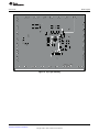
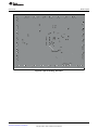
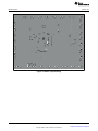
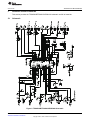
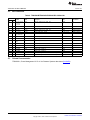
User's Guide
SLVU394 – October 2010
TPS65023B/TPS650231EVM
The characteristics, operation, and use of the TPS65023B/TPS650231EVM-664 evaluation module (EVM)
are described in this document. This EVM is designed to help the user evaluate and test the various
operating modes of the TPS65023B/TPS650231. This user’s guide includes setup instructions for the
hardware and software, a schematic diagram, a bill of materials, and PCB layout drawings for the
evaluation module.
1
2
3
4
5
Contents
Introduction .................................................................................................................. 1
Electrical Performance Specification ..................................................................................... 2
Input/Output Connector Description ...................................................................................... 3
Board Layout ................................................................................................................ 6
Schematic and Bill of Materials .......................................................................................... 11
List of Figures
1
Assembly Layer ............................................................................................................. 6
2
Top Layer Routing .......................................................................................................... 7
3
Layer-2 Routing, GND Plane .............................................................................................. 8
4
Layer-3 Routing, Vin Plane ................................................................................................ 9
5
Bottom Layer Routing ..................................................................................................... 10
6
TPS65023B/TPS650231EVM-664 Schematic ......................................................................... 11
1
EVM Ordering Options ..................................................................................................... 2
2
Default LDO Output Voltages TPS65023B .............................................................................. 2
3
Default LDO Output Voltages TPS650231 .............................................................................. 2
4
TPS65023B/TPS650231EVM-664 Bill of Materials ................................................................... 12
List of Tables
1
Introduction
The Texas Instruments TPS65023B/TPS650231EVM is an integrated power management integrated
circuit (IC) for applications that are powered with one Li-ion or Li-polymer cell and require multiple power
rails. The TPS65023B/TPS650231 contains three highly efficient switching step-down converters, two
LDOs, and additional status and I/O pins. The device is controlled via an I2C interface (HPA172).
1.1
Requirements
In order for this EVM to operate properly, the following components must be connected and properly
configured.
1.1.1
Personal Computer
A personal computer with a USB port is required to operate this EVM. The TPS65023B/TPS650231
interface software, which is run on the personal computer (PC), communicates with the EVM via the PC
USB port. The user sends commands to the EVM as well as reads the contents of the
TPS65023B/TPS650231 internal registers through the USB port.
SLVU394 – October 2010
Submit Documentation Feedback
TPS65023B/TPS650231EVM
Copyright © 2010, Texas Instruments Incorporated
1
Electrical Performance Specification
1.1.2
www.ti.com
Printed-Circuit Board Assembly
The TPS65023B/TPS650231EVM-664 PCB contains the TPS65023B/TPS650231 IC and its required
external components. This board contains several jumpers and connectors that allow the user to
customize the board for specific operating conditions.
USB-to- I 2C Adapter
1.1.3
The USB-to-I2C Adapter, also known as the HPA172, is the link that allows the PC and the EVM to
communicate. The adapter connects to the PC with the supplied USB cable on one side and to the EVM
though the supplied ribbon cable on the other. When the user writes a command to the EVM, the interface
program, which is run from the PC, sends the command to the PC USB port. The adapter receives the
USB command and converts the signal to an I2C protocol. It then sends the I2C signal to the
TPS65023B/TPS650231 board. When the user reads a status register from the EVM, the PC sends a
command to read a register on the EVM. When the EVM receives the command, it reports the status of
the register via the I2C interface. The adapter receives the information on the I2C interface, converts it to a
USB protocol, and sends it to the PC.
1.1.4
Software
Texas Instruments provides software to assist the user in evaluating this EVM. To install the software, go
to the Texas Instruments Web page and download the latest software version from the TPS65023B or
TPS650231 product folder. Once you have downloaded the software, execute the setup file, and follow
the instructions given.
1.2
Features
•
•
•
•
•
2
Three high-efficiency DC/DC step-down converters (1.7 A/1.2 A/1 A)
2 x 200-mA low-dropout (LDO) regulators
30-mA RTC (Reel Time Clock) LDO
I2C Interface (100-ns setup and hold time)
Dynamic voltage scaling DCDC1
Electrical Performance Specification
Table 1. EVM Ordering Options
Default Output Voltages
Orderable EVM
Number
Device Part
Number
DCDC1
DCDC2
DCDC3
LDO1
LDO2
TPS65023BEVM-664
TPS65023B
1.2V / 1.6V
1/8V / 3.3V
1.8V / 3.3V
SeeTable 2
SeeTable 2
TPS650231EVM-664
TPS650231
1.2V / 1.6V
n/a
1.8V / 3.3V
See Table 3
See Table 3
Table 2. Default LDO Output Voltages TPS65023B
DEFLDO2
DEFLDO1
VLDO1
VLDO2
0
0
1.3 V
3.3 V
0
1
2.8 V
3.3 V
1
0
1.3 V
1.8 V
1
1
1.8 V
3.3 V
Table 3. Default LDO Output Voltages TPS650231
2
DEFLDO2
DEFLDO1
VLDO1
VLDO2
0
0
1.3 V
3.3 V
0
1
2.8 V
3.3 V
1
0
1.3 V
1.8 V
1
1
2.1 V
3.3 V
TPS65023B/TPS650231EVM
SLVU394 – October 2010
Submit Documentation Feedback
Copyright © 2010, Texas Instruments Incorporated
Input/Output Connector Description
www.ti.com
3
Input/Output Connector Description
This section describes the jumpers and connectors on the EVM, as well as how to properly connect, set
up, and use the TPS65023B/TPS650231EVM-664.
J1 – VIN
Input voltage from external power supply, recommended maximum 5.5 V. Input current depends
on load but typically is less than 2 A.
J2 – GND
This is the return connection for VIN.
J3 – VINLDO/GND
Input voltage and return for LDO1 and LDO2. Resistor R20 connects this pin to VIN. If an
external power supply is used, remove R20. Recommended maximum input voltage is 5.5 V.
J4 – VSYSIN/GND
Input voltage and return for VSYSIN, one of the input voltages for RTC. Resistor R21 can be
used to connect this input to VIN. If an external power supply is used, remove R21.
Recommended maximum input voltage is 4 V.
J5 – VBACKUP/GND
Input voltage and return for VBACKUP, one of the input voltages for RTC. There are no onboard
connections to a voltage input. Recommended maximum input voltage is 4 V.
J6 – VRTC/GND
Output voltage from RTC circuit.
J7 – Fault Outputs
Four fault outputs are available on this connector:
PWRFAIL – Fault occurs when input voltage is less than 3 V. Pulled up to VRTC when safe; low
for fail.
INT – Fault occurs when a fail is on an input or output voltage; acts as a sum fail. Pulled up to
VIN when safe; low for fail.
RESPWRON – Low reset signal is controlled by SW1, 144 ms. Pulled up to VIN normally.
LOWBAT – Fault occurs when input voltage is less than 3.6 V. Pulled up to VIN when safe; low
for fail.
J8 – I2C
This header duplicates the I2C signals from the J20 interface connector. I2C data (SDA) and
clock (SCL) can be accessed on this header
J9 – VDCDC1
Output from DCDC1 switching regulator maximum output current 1.7 A; default voltage setting is
3.3 V.
J10 – GND
Return for VDCDC1.
J11 – VDCDC2
Output from DCDC2 switching regulator; maximum output current 1.2 A.
J12 – GND
Return for VDCDC2
J13 – VLDO1
Output from low-dropout regulator VLDO1; maximum output current 200 mA.
J14 – GND
Return for VLDO1
J15 – VLDO2
Output from low-dropout regulator VLDO2; maximum output current 200 mA.
J16 – GND
Return for VLDO2.
SLVU394 – October 2010
Submit Documentation Feedback
TPS65023B/TPS650231EVM
Copyright © 2010, Texas Instruments Incorporated
3
Input/Output Connector Description
www.ti.com
J17 – VDCDC3
Output from switching regulator DCDC3; maximum output current 1 A.
J18– GND
Return for VDCDC3.
J19 –
J19 is the interface connector for the I2C interface. Connect a 10-pin ribbon cable between J13
and the USB-to-GPIO interface.
JP1 – DEF1
Sets default voltage for DCDC1, 1.2 V or 1.6 V.
JP2 – DEF2
Sets default voltage for DCDC2, 3.3 V or 1.8 V, in TPS65023B (HPA664-001) configuration. In
the TPS650231, no default output voltage options are available. In this case, the output voltage
is adjustable with an external voltage divider R3, R2. The default setup is 1.2 V in the factory
EVM (HPA664-002) configuration. See section x for advanced voltage scaling options..
JP3 – DEF3
Sets default voltage for DCDC3, 3.3 V or 1.8 V.
JP4 – DCDC1 ON/OFF
EN for DCDC1 converter; default setting is ON
JP5 – DCDC2 ON/OFF
EN for DCDC2 converter; default setting is ON.
JP6 – DCDC3 ON/OFF
EN for DCDC3 converter; default setting is ON.
JP7 – LDO ON/OFF
EN for both LDO1 and LDO2 regulators; default setting is ON.
JP8 – DEFLDO1
Sets default voltage for LDO1 and LDO2 in combination with DEFLDO2. (See Table 2 for
TPS65023B and Table 3 for TPS650231 - defaults LDO output voltages.)
JP9 – DEFLDO2
Sets default voltage for LDO1 and LDO2 in combination with DEFLDO1. (See Table 2 for
TPS65023B and Table 3 for TPS650231 - defaults LDO output voltages.)
S1 – HOT_RST
S1 is a normally open, momentary pushbutton switch that, when pressed, connects the
HOT_RST input of the TPS650231 to GND, generating the HOT_RESET pulse. HOT_RESET
pin is pulled up externally.
3.1
Setup
The following steps must be followed before the EVM can be operated.
1. Install the TPS65023B/TPS650231EVM software.
2. Connect input voltages and loads to the EVM.
3. Configure all EVM jumpers to factory setting.
JP4–ON
JP2–1.8V
JP7–ON
4
JP1–1.6V
JP5–ON
JP9–High
JP3–1.8V
JP6–ON
JP8–High
TPS65023B/TPS650231EVM
SLVU394 – October 2010
Submit Documentation Feedback
Copyright © 2010, Texas Instruments Incorporated
Input/Output Connector Description
www.ti.com
4.
5.
6.
7.
3.2
3.2.1
Connect the ribbon cable between the EVM and the USB-TO-GPIO (HPA172) adapter.
Connect the USB cable between the computer and the HPA172EVM.
Turn on all supplies.
Run the TPS65023B/TPS650231EVM software
Modifications
Setting the Output Voltage
The TPS65023B features two default output voltages. These output voltages can be selected by pulling
DEFDCDC2 high – selecting the higher default output voltage – or pulling DEFDCDC2 low – selecting the
lower default output voltage.
In addition, the output voltage of DCDC2 can be externally adjusted with the resistor divider network R3
and R6. The default configuration of the TPS65023BEVM-664 is that R3 and R6 are not assembled. The
default output voltage of DCDC2 can be selected with JP2.
Note that the default output voltage is selected once at startup of the device. Changing logic level of
DEFDCDC2 during operation does not affect the output voltage and is not allowed.
3.2.2
Setting the Output Voltage for DCDC2, TPS650231
The TPS650231 does not feature these default output voltages. The output voltages of DCDC2 is
externally adjustable only. The default configuration of the TPS650231EVM-664 is that R3 and R6 are not
assembled. JP2 is not assembled.
TPS650231 does not have the default output voltage feature, and this provides the benefit of external
voltage scaling options.
3.2.3
Simple Two-Point Voltage Scaling, TPS650231
DCDC2 does not have the previously described preset default output voltages. An external voltage scaling
circuit is on the EVM, and the output voltage of DCDC2 can be switched between two preset voltages.
This useful feature reduces the power consumption of an application processor in Low Power mode.
The voltage scaling circuit consists of JP2,Q1, R3, R6, and R24. The circuit uses a transistor (Q1) to
connect a resistor (R24) in parallel to the lower resistor of the feedback network (R6) of DCDC2.
Modifying the resistor network by paralleling R24 and R6 reduces the overall resistance of the lower
resistor and therefore increases the output voltage of the DC/DC converter. See Equation 1 and
Equation 2 to design R24. In the factory configuration, the components JP2, Q1, and R24 are not
assembled on the board.
3.2.4
Scaling the Output Voltage of DCDC2 From LDO2
Another approach to scale the DC/DC converter output voltage is to use an external adjustable voltage.
Any external adjustable voltage source can be used, e.g., output voltage of an digital-to-analog converter.
In the TPS65023B/TPS650231, LDO1 and LDO2 can be adjusted via I2C. The TPS65023B/TPS650231
provides the ability to feed the output voltage of LDO2 back to the resistor divider network, using R25, and
therefore scale the output voltage of DCDC2 based on the LDO2 output voltage.
In this configuration, R25, R3, and R6 need to be assembled. R24, R26, Q1, and R3 need to be removed.
Vout _ DCDC2 = V _ REF ´ (1 +
R1
R1
)) + ( V _ REF - VLDO2) ´ ( )
R3
R2
(1)
From Equation 2 it can be seen that maximum DCDC1 output voltage occurs for minimum VLDO2, and
minimum DCDC1 output voltage occurs for maximum VLDO2.
To ensure that the desired DCDC1 output voltages can be adjusted, design the resistors R25, R3, and R6
according to and Equation 2 and Equation 2.
SLVU394 – October 2010
Submit Documentation Feedback
TPS65023B/TPS650231EVM
Copyright © 2010, Texas Instruments Incorporated
5
Board Layout
www.ti.com
Vout _ DCDC2, min = V _ REF ´ (1 +
R1
R1
)) + ( V _ REF - VLDO2, max) ´ ( )
R3
R2
(2)
Vout _ DCDC2, max = V _ REF ´ (1 +
R1
R1
)) + ( V _ REF - VLDO2, min) ´ ( )
R3
R2
(3)
The most straight forward way is to choose a value for R6 according to the recommendations in the
converter data sheet.
4
Board Layout
This section provides the TPS65023B/TPS650231EVM-664 board layout and illustrations.
4.1
Layout
Board layout is critical for all switch mode power supplies. Figure 1 through Figure 5 show the board
layout for the TPS65023B/TPS650231EVM-664 PCB. The nodes with high switching frequencies and
currents are short and are isolated from the noise-sensitive feedback circuitry. Careful attention has been
given to the routing of high-frequency current loops. See the data sheet for specific layout guidelines.
Figure 1. Assembly Layer
6
TPS65023B/TPS650231EVM
SLVU394 – October 2010
Submit Documentation Feedback
Copyright © 2010, Texas Instruments Incorporated
Board Layout
www.ti.com
Figure 2. Top Layer Routing
SLVU394 – October 2010
Submit Documentation Feedback
TPS65023B/TPS650231EVM
Copyright © 2010, Texas Instruments Incorporated
7
Board Layout
www.ti.com
Figure 3. Layer-2 Routing, GND Plane
8
TPS65023B/TPS650231EVM
SLVU394 – October 2010
Submit Documentation Feedback
Copyright © 2010, Texas Instruments Incorporated
Board Layout
www.ti.com
Figure 4. Layer-3 Routing, Vin Plane
SLVU394 – October 2010
Submit Documentation Feedback
TPS65023B/TPS650231EVM
Copyright © 2010, Texas Instruments Incorporated
9
Board Layout
www.ti.com
Figure 5. Bottom Layer Routing
10
TPS65023B/TPS650231EVM
SLVU394 – October 2010
Submit Documentation Feedback
Copyright © 2010, Texas Instruments Incorporated
Schematic and Bill of Materials
www.ti.com
5
Schematic and Bill of Materials
This section provides the TPS65023B/TPS650231EVM-664 schematic and bill of materials.
5.1
Schematic
Figure 6. TPS65023B/TPS650231EVM-664 Schematic
SLVU394 – October 2010
Submit Documentation Feedback
TPS65023B/TPS650231EVM
Copyright © 2010, Texas Instruments Incorporated
11
Schematic and Bill of Materials
5.2
www.ti.com
Bill of Materials
Table 4. TPS65023B/TPS650231EVM-664 Bill of Materials
Count
RefDes
Value
Description
Size
Part Number
9
C1, C2, C4, C9,
C10, C11,
C14–C16
10 µF
Capacitor, Ceramic, 6.3V, X5R, 10%
0805
Std
4
4
C3, C6, C7, C17
1.0 µF
Capacitor, Ceramic, 6.3V, X5R,10%
0603
Std
1
1
C5
1500 pF
Capacitor, Ceramic, 50V, X7R, 10%
0603
C1608X7R1H152K
4
4
C8, C18
2.2 µF
Capacitor, Ceramic, 6.3V, X5R, 10%
0603
C1608X5R0J225K
3
3
L1, L2, L3
2.2 µH
Inductor, SMT, 2.0A, 110mΩ
0.157 x 0.157
LPS3015-222ML
0
0
R1, R2, R4–R6,
R17, R18, R21
Open
Resistor, Chip, 1/16W, 1%
0603
Std
0
1
R3
182k
Resistor, Chip, 1/16W, 1%
0603
Std
0
1
R6
365k
Resistor, Chip, 1/16W, 1%
0603
Std
6
6
R7, R11–R14,
R22
100k
Resistor, Chip, 1/16W, 1%
0603
Std
1
1
R8
10
Resistor, Chip, 1/16W, 1%
0603
Std
1
1
R9
1.20M
Resistor, Chip, 1/16W, 1%
0603
Std
1
1
R10
499k
Resistor, Chip, 1/16W, 1%
0603
Std
2
2
R15, R16
4.75k
Resistor, Chip, 1/16W, 1%
0603
Std
2
2
R19, R20
0
Resistor, Chip, 1/16W, 5%
0603
Std
1
0
U1
TPS65023BRSB
IC, Power Management IC for Li-Ion Powered Systems
QFN
TPS65023BRSB
0
1
U1
TPS650231RSB
IC, Power Management IC for Li-Ion Powered Systems
QFN
TPS650231RSB
-001
-002
9
5.3
Related Documentation
TPS650231, Power Management IC For Li-Ion Powered Systems data sheet (SLVSAE3)
12
TPS65023B/TPS650231EVM
SLVU394 – October 2010
Submit Documentation Feedback
Copyright © 2010, Texas Instruments Incorporated
Evaluation Board/Kit Important Notice
Texas Instruments (TI) provides the enclosed product(s) under the following conditions:
This evaluation board/kit is intended for use for ENGINEERING DEVELOPMENT, DEMONSTRATION, OR EVALUATION
PURPOSES ONLY and is not considered by TI to be a finished end-product fit for general consumer use. Persons handling the
product(s) must have electronics training and observe good engineering practice standards. As such, the goods being provided are
not intended to be complete in terms of required design-, marketing-, and/or manufacturing-related protective considerations,
including product safety and environmental measures typically found in end products that incorporate such semiconductor
components or circuit boards. This evaluation board/kit does not fall within the scope of the European Union directives regarding
electromagnetic compatibility, restricted substances (RoHS), recycling (WEEE), FCC, CE or UL, and therefore may not meet the
technical requirements of these directives or other related directives.
Should this evaluation board/kit not meet the specifications indicated in the User’s Guide, the board/kit may be returned within 30
days from the date of delivery for a full refund. THE FOREGOING WARRANTY IS THE EXCLUSIVE WARRANTY MADE BY
SELLER TO BUYER AND IS IN LIEU OF ALL OTHER WARRANTIES, EXPRESSED, IMPLIED, OR STATUTORY, INCLUDING
ANY WARRANTY OF MERCHANTABILITY OR FITNESS FOR ANY PARTICULAR PURPOSE.
The user assumes all responsibility and liability for proper and safe handling of the goods. Further, the user indemnifies TI from all
claims arising from the handling or use of the goods. Due to the open construction of the product, it is the user’s responsibility to
take any and all appropriate precautions with regard to electrostatic discharge.
EXCEPT TO THE EXTENT OF THE INDEMNITY SET FORTH ABOVE, NEITHER PARTY SHALL BE LIABLE TO THE OTHER
FOR ANY INDIRECT, SPECIAL, INCIDENTAL, OR CONSEQUENTIAL DAMAGES.
TI currently deals with a variety of customers for products, and therefore our arrangement with the user is not exclusive.
TI assumes no liability for applications assistance, customer product design, software performance, or infringement of
patents or services described herein.
Please read the User’s Guide and, specifically, the Warnings and Restrictions notice in the User’s Guide prior to handling the
product. This notice contains important safety information about temperatures and voltages. For additional information on TI’s
environmental and/or safety programs, please contact the TI application engineer or visit www.ti.com/esh.
No license is granted under any patent right or other intellectual property right of TI covering or relating to any machine, process, or
combination in which such TI products or services might be or are used.
FCC Warning
This evaluation board/kit is intended for use for ENGINEERING DEVELOPMENT, DEMONSTRATION, OR EVALUATION
PURPOSES ONLY and is not considered by TI to be a finished end-product fit for general consumer use. It generates, uses, and
can radiate radio frequency energy and has not been tested for compliance with the limits of computing devices pursuant to part 15
of FCC rules, which are designed to provide reasonable protection against radio frequency interference. Operation of this
equipment in other environments may cause interference with radio communications, in which case the user at his own expense
will be required to take whatever measures may be required to correct this interference.
EVM Warnings and Restrictions
It is important to operate this EVM within the input voltage range of 3.3 V to 5.5 V and the output voltage range of 0.8 V to 3.3 V .
Exceeding the specified input range may cause unexpected operation and/or irreversible damage to the EVM. If there are
questions concerning the input range, please contact a TI field representative prior to connecting the input power.
Applying loads outside of the specified output range may result in unintended operation and/or possible permanent damage to the
EVM. Please consult the EVM User's Guide prior to connecting any load to the EVM output. If there is uncertainty as to the load
specification, please contact a TI field representative.
During normal operation, some circuit components may have case temperatures greater than 60°C. The EVM is designed to
operate properly with certain components above 60°C as long as the input and output ranges are maintained. These components
include but are not limited to linear regulators, switching transistors, pass transistors, and current sense resistors. These types of
devices can be identified using the EVM schematic located in the EVM User's Guide. When placing measurement probes near
these devices during operation, please be aware that these devices may be very warm to the touch.
Mailing Address: Texas Instruments, Post Office Box 655303, Dallas, Texas 75265
Copyright © 2010, Texas Instruments Incorporated
IMPORTANT NOTICE
Texas Instruments Incorporated and its subsidiaries (TI) reserve the right to make corrections, modifications, enhancements, improvements,
and other changes to its products and services at any time and to discontinue any product or service without notice. Customers should
obtain the latest relevant information before placing orders and should verify that such information is current and complete. All products are
sold subject to TI’s terms and conditions of sale supplied at the time of order acknowledgment.
TI warrants performance of its hardware products to the specifications applicable at the time of sale in accordance with TI’s standard
warranty. Testing and other quality control techniques are used to the extent TI deems necessary to support this warranty. Except where
mandated by government requirements, testing of all parameters of each product is not necessarily performed.
TI assumes no liability for applications assistance or customer product design. Customers are responsible for their products and
applications using TI components. To minimize the risks associated with customer products and applications, customers should provide
adequate design and operating safeguards.
TI does not warrant or represent that any license, either express or implied, is granted under any TI patent right, copyright, mask work right,
or other TI intellectual property right relating to any combination, machine, or process in which TI products or services are used. Information
published by TI regarding third-party products or services does not constitute a license from TI to use such products or services or a
warranty or endorsement thereof. Use of such information may require a license from a third party under the patents or other intellectual
property of the third party, or a license from TI under the patents or other intellectual property of TI.
Reproduction of TI information in TI data books or data sheets is permissible only if reproduction is without alteration and is accompanied
by all associated warranties, conditions, limitations, and notices. Reproduction of this information with alteration is an unfair and deceptive
business practice. TI is not responsible or liable for such altered documentation. Information of third parties may be subject to additional
restrictions.
Resale of TI products or services with statements different from or beyond the parameters stated by TI for that product or service voids all
express and any implied warranties for the associated TI product or service and is an unfair and deceptive business practice. TI is not
responsible or liable for any such statements.
TI products are not authorized for use in safety-critical applications (such as life support) where a failure of the TI product would reasonably
be expected to cause severe personal injury or death, unless officers of the parties have executed an agreement specifically governing
such use. Buyers represent that they have all necessary expertise in the safety and regulatory ramifications of their applications, and
acknowledge and agree that they are solely responsible for all legal, regulatory and safety-related requirements concerning their products
and any use of TI products in such safety-critical applications, notwithstanding any applications-related information or support that may be
provided by TI. Further, Buyers must fully indemnify TI and its representatives against any damages arising out of the use of TI products in
such safety-critical applications.
TI products are neither designed nor intended for use in military/aerospace applications or environments unless the TI products are
specifically designated by TI as military-grade or "enhanced plastic." Only products designated by TI as military-grade meet military
specifications. Buyers acknowledge and agree that any such use of TI products which TI has not designated as military-grade is solely at
the Buyer's risk, and that they are solely responsible for compliance with all legal and regulatory requirements in connection with such use.
TI products are neither designed nor intended for use in automotive applications or environments unless the specific TI products are
designated by TI as compliant with ISO/TS 16949 requirements. Buyers acknowledge and agree that, if they use any non-designated
products in automotive applications, TI will not be responsible for any failure to meet such requirements.
Following are URLs where you can obtain information on other Texas Instruments products and application solutions:
Products
Applications
Amplifiers
amplifier.ti.com
Audio
www.ti.com/audio
Data Converters
dataconverter.ti.com
Automotive
www.ti.com/automotive
DLP® Products
www.dlp.com
Communications and
Telecom
www.ti.com/communications
DSP
dsp.ti.com
Computers and
Peripherals
www.ti.com/computers
Clocks and Timers
www.ti.com/clocks
Consumer Electronics
www.ti.com/consumer-apps
Interface
interface.ti.com
Energy
www.ti.com/energy
Logic
logic.ti.com
Industrial
www.ti.com/industrial
Power Mgmt
power.ti.com
Medical
www.ti.com/medical
Microcontrollers
microcontroller.ti.com
Security
www.ti.com/security
RFID
www.ti-rfid.com
Space, Avionics &
Defense
www.ti.com/space-avionics-defense
RF/IF and ZigBee® Solutions www.ti.com/lprf
Video and Imaging
www.ti.com/video
Wireless
www.ti.com/wireless-apps
Mailing Address: Texas Instruments, Post Office Box 655303, Dallas, Texas 75265
Copyright © 2010, Texas Instruments Incorporated