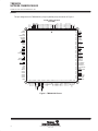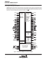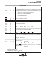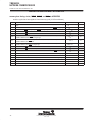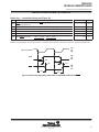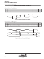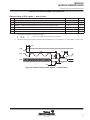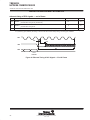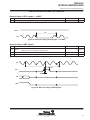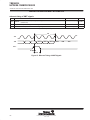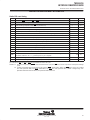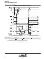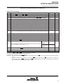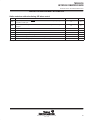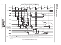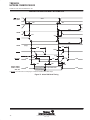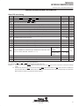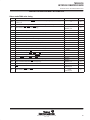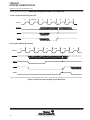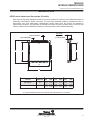
1
TMS380C26 NETWORK COMMPROCESSOR SPWS010A–APRIL 1992–REVISED MARCH 1993 • • • • • • • • • • • • • • • IEEE 802.5 and IBM Token-Ring Network Compatible IEEE 802.3 and Blue Book Ethernet Network Compatible Pin and Software Compatible With the TMS380C16 Configurable Network Type and Speed: – Selectable by Host Software Control (Adapter Control Register) – Selectable by Network Front-End – Readable from Host (Adapter Control Register) • • Token-Ring Features – 16- or 4-Megabit-per-Second Data Rates – Supports up to 18K-Byte Frame Size (16 Mbps Operation Only) – Supports Universal and Local Network Addressing – Early Token Release Option (16 Mbps Operation Only) – Compatible With the TMS38054 • • • • Ethernet Features – 10-Megabit-per-Second Data Rate – Compatible With Most Ethernet Serial Network Interface Devices – Full Duplex Ethernet Operation Allows Network Speed Self-test • • • • • • • Expandable Local LAN Subsystem Memory Space up to 2 Megabytes Supports Multicast Addressing of Network Group Addresses Through Hashing Glueless Interface to DRAMs • High-Performance 16-Bit CPU for Communications Protocol Processing Low-Cost Host-Slave I/O Interface Option Up to 32-Bit Host Address Bus Selectable Host System Bus Options 80x8x or 68xxx-Type Bus and Memory Organization – 8- or 16-Bit Data Bus on 80x8x Buses – Optional Parity Checking Dual-Port DMA and Direct I/O Transfers to Host Bus Specification for External Adapter-Bus Devices (SEADs) Supports External Hardware Interface for User-Defined External Logic Enhanced Address Copy Option (EACO) Interface Supports External Address Checking Logic for Bridging or External Custom Applications Support for Module High-Impedance In-Circuit Testing Built-in Real-Time Error Detection Bring-Up and Self-Test Diagnostics With Loopback Automatic Frame Buffer Management Slow-Clock Low-Power Mode Single 5-V Supply 1-µm CMOS Technology 250 mA Typical Latch-Up Immunity at 25°C ESD Protection Exceeds 2,000 V 132-Pin JEDEC Plastic Quad Flat Package (PQ Suffix) Operating Temperature Range 0°C to 70 °C Up to 8 Megabyte-per-Second High-Speed Bus Master DMA Interface network commprocessor applications diagram LAN Subsystem Transmit Attached System Bus TMS380C26 Token Ring or Ethernet Physical Layer Circuitry To Network Receive Memory Copyright 1993, Texas Instruments Incorporated PRODUCTION DATA information is current as of publication date. Products conform to specifications per the terms of Texas Instruments standard warranty. Production processing does not necessarily include testing of all parameters. • POST OFFICE BOX 1443 HOUSTON, TEXAS 77251–1443 1 TMS380C26 NETWORK COMMPROCESSOR SPWS010A–APRIL 1992–REVISED MARCH 1993 pinout The pin assignments for TMS380C26 (132-pin quad flat-pack) are shown in Figure 1. 119 118 117 123 122 121 120 127 126 125 124 131 130 129 128 4 3 2 1 132 8 7 6 5 12 11 10 9 79 80 81 82 75 76 77 78 71 72 73 74 67 68 69 70 63 64 65 66 59 69 61 62 55 56 57 58 51 52 53 54 83 116 115 114 113 112 111 110 109 108 107 106 105 104 103 102 101 100 99 98 97 96 95 94 93 92 91 80 89 88 87 86 85 84 18 19 20 21 22 23 24 25 26 27 28 29 30 31 32 33 34 35 36 37 38 39 40 41 42 43 44 45 46 47 48 49 50 VSS5 SADL2 SADL1 SADL0 SPL SHRQ/SBRQ SBHE/SRNW SDBEN SOWN SRDY/SDTACK SRD/SUDS SPH SADH7 SADH6 VSSC VDD6 VSS6 SADH5 SADH4 SADH3 SADH2 SADH1 SADH0 TEST5 TEST4 TEST3 TEST2 TEST1 TEST0 XFAIL XMATCH VDD1 VSSL VDDL CLKDIV VSSC NSELOUT0 PRTYEN BTSTRP SIACK SRESET SRS1 SRS0 SRSX SCS SBRLS SBBSY S8/SHALT SRS2/SBERR VDDL SI/M SINTR/SIRQ SHLDA/SBGR SDDIR SRAS/SAS SWR/SLDS VSSI SXAL SALE SBCLK SADL7 SADL6 SADL5 SADL4 SADL3 VDD5 16 15 14 13 17 V SSL V DD4 NMI EXTINT0 EXTINT1 EXTINT2 EXTINT3 MADL0 MADL1 MADL2 MADL3 MADL4 MADL5 MADL6 MADL7 MAXPL V SS4 MBGR MBGQ MAXPH MADH0 MADH1 MADH2 MADH3 V SS3 V DD3 MADH4 MADH5 MADH6 MADH7 MBEN MOE V SS1 132-PIN QUAD FLAT PACK (TOP VIEW) Figure 1. TMS380C26 Pinout 2 • POST OFFICE BOX 1443 HOUSTON, TEXAS 77251–1443 VSSC MRAS MW MCAS MAX2 MAX0 MDDIR VDD2 SYNCIN OSCIN VSS2 MROMEN MACS MAL MREF MBIAEN VDDL MRESET MBCLK2 MBCLK1 OSCOUT RCVR/RXD RCLK/RXC NSETOUT1 PXTALIN/TXC VSS1 WRAP/TXEN DRVR DRVR WFLT/COLL NSRT/LPBK FRAQ/TXD REDY/CRS TMS380C26 NETWORK COMMPROCESSOR SPWS010A–APRIL 1992–REVISED MARCH 1993 description The TMS380C26 is a single-chip network communications processor (commprocessor) that supports token ring, or Ethernet Local Area Networks (LANs). Either token ring at data rates of 16 Mbps or 4 Mbps, or Ethernet at a data rate of 10 Mbps, can be selected. A flexible configuration scheme allows network type and speed to be configured by hardware or software. This allows the design of LAN subsystems which support both token ring and Ethernet networks, by electrically or physically switched network front-end circuits. The TMS380C26 conforms to IEEE 802.5–1989 standards and has been verified to be completely IBM Token-Ring compatible. By integrating the essential control building blocks needed on a LAN subsystem card into one device, the TMS380C26 can ensure that this IBM compatability is maintained in silicon. The TMS380C26 conforms to ISO/IEC 8802–3 (ANSI/IEEE Std 802.3) CSMA/CD standards, and the Ethernet ”Blue Book” standard. The high degree of integration of the TMS380C26 makes it a virtual LAN subsystem on a single chip. Protocol handling, host system interfacing, memory interfacing, and communications processing are all provided through the TMS380C26. To complete LAN subsystem design, only the network interface hardware, local memory, and minimal additional components such as PALs and crystal oscillators need to be added. The TMS380C26 provides a 32-bit system memory address reach with a high-speed bus-master DMA interface that supports rapid communications with the host system. In addition, the TMS380C26 supports direct I/O and a low-cost 8-bit pseudo-DMA interface that requires only a chip select to work directly on an 80x8x 8-bit slave I/O interface. Finally, selectable 80x8x or 68xxx-type host system bus and memory organization add to design flexibility. The TMS380C26 supports addressing for up to two Megabytes of local memory. This expanded memory capacity can improve LAN subsystem performance by minimizing the frequency of host LAN subsystem communications by allowing larger blocks of information to be transferred at one time. The support of large local memory is important in applications that require large data transfers (such as graphics or data base transfers) and in heavily loaded networks where the extra memory can provide data buffers to store data until it can be processed by the host. The proprietary CPU used in the TMS380C26 allows protocol software to be downloaded into RAM or stored in ROM in the local memory space. By moving protocols (such as LLC) to the LAN subsystem, overall system performance is increased. This is accomplished due to the the offloading of processing from the host system to the TMS380C26, which may also reduce LAN subsystem-to-host communications. As other protocol software is developed, greater differentiation of end products with enhanced system performance will be possible. In addition, the TMS380C26 includes hardware counters that provide realtime error detection and automatic frame buffer management. These counters control system bus retries, burst size, and track host and LAN subsystem buffer status. Previously, these counters needed to be maintained in software. By integrating them into hardware, software overhead is removed and LAN subsystem performance is improved. The TMS380C26 implements a TI-patented Enhanced Address Copy Option (EACO) interface. This interface supports external address checking devices, such as the TMS380SRA Source Routing Accelerator. The TMS380C26 has a 128-word external I/O space in its memory map to support external address-checker devices and other hardware extensions to the TMS380 architecture. Hardware designed in conformance with TI’s Specification for External Adapter-bus Devices (SEADs) can map registers into this external I/O space and post interrupts to the TMS380C26. The major blocks of the TMS380C26 include the Communications Processor (CP), System Interface (SIF), Memory Interface (MIF), Protocol Handler (PH), Clock Generator (CG), and the Adapter Support Function (ASF) as shown in Figure 2. The TMS380C26 is available in a 132-pin JEDEC plastic quad flat pack and is rated from 0°C to 70°C. IBM is a registered trademark of International Business Machines Corporation. • POST OFFICE BOX 1443 HOUSTON, TEXAS 77251–1443 3 TMS380C26 NETWORK COMMPROCESSOR SPWS010A–APRIL 1992–REVISED MARCH 1993 block diagram and signal descriptions TMS380C26 has a bus interface to the host system, a bus interface to local memory, and an interface to the physical layer circuitry. As a rule of thumb in the pin nomenclature and descriptions that follow, pin names starting with the letter S attach to the host system bus and pin names starting with the letter M attach to the local memory bus. Active-low signals have names with overbars, e.g., SCS. SADH0 SADH7 SADL0 SADL7 SPH SPL SBRLS SINTR/SIRQ SDDIR SDBEN SALE SXAL SOWN SIACK SBCLK SRD/SUDS SWR/SLDS SRDY/SDTACK SI/M SHLDA/SBGR SBHE/SRNW SRAS/SAS S8/SHALT SRESET SRS0 SRS1 SRS2/SBERR SCS SRSX SHRQ/SBRQ SBBSY BTSTRP PRTYEN NSELOUT0 NSELOUT1 System Interface (SIF) Memory Interface (MIF) • DIO Control • Bus Control • DMA Control • DRAM Refresh • Local Bus Arbitrator • Local Bus Control • Local Parity Check/ Generator Clock Generator (CG) Adapter Support Function (ASF) Communications Processor • Interrupts • Test Function MADH0 MADH7 MADL0 MADL7 MRAS MCAS MAXPH MAXPL MW MOE MDDIR MAL MAX0 MAX2 MRESET MROMEN MBEN MBRQ MBGR MACS MBIAEN MREF OSCIN OSCOUT MBCLK1 MBCLK2 SYNCIN CLKDIV NMI EXTINT0 EXTINT3 TEST0 TEST5 XMATCH XFAIL RCLK/RXC REDY/CRS WFLT/COLL RCVR/RXD PXTALIN/TXC Protocol Handler (PH): for Token Ring and Ethernet Interface Figure 2. TMS380C26 COMMprocessor Block Diagram 4 • POST OFFICE BOX 1443 HOUSTON, TEXAS 77251–1443 FRAQ/TXD NSRT/LPBK WRAP/TXEN DRVR DRVR TMS380C26 NETWORK COMMPROCESSOR SPWS010A–APRIL 1992–REVISED MARCH 1993 Terminal Functions PIN NAME BTSTRP NO. 23 I/O IN DESCRIPTION Bootstrap. The value on this pin is loaded into the BOOT bit of the SIFACL register at reset (i.e., when the SRESET pin is asserted or the ARESET bit in the SIFACL register is set) to form a default value. This bit indicates whether chapters 0 and 31 of the memory map are RAM or ROM. If these chapters are RAM then the TMS380C26 is denied access to the local memory bus until the CPHALT bit in the SIFACL register is cleared. H = Chapters 0 and 31 of local memory are RAM-based (see Note 1). L = Chapters 0 and 31 of local memory are ROM-based. Clock Divider Select. This pin must be pulled high CLKDIV 19 IN EXTINT0 EXTINT1 EXTINT2 EXTINT3 14 13 12 11 IN Reserved; must be pulled high (see Note 4). MACS 104 IN Reserved. Must be tied low (see Note 2). MADH0 MADH1 MADH2 MADH3 MADH4 MADH5 MADH6 MADH7 129 128 127 126 123 122 121 120 MADL0 MADL1 MADL2 MADL3 MADL4 MADL5 MADL6 MADL7 10 9 8 7 6 5 4 3 MAL 103 I/O H = Indicates 64-MHz OSCIN (see Note 3). L = Reserved. Local memory Address, Data and Status Bus – high byte. For the first quarter of the local memory cycle these bus lines carry address bits AX4 and A0 to A6; for the second quarter, they carry status bits; and for the third and fourth quarters, they carry data bits 0 to 7. The most significant bit is MADH0 and the least significant bit is MADH7. Signal I/O 4Q D0–D7 Local Memory Address, Data and Status Bus – low byte. For the first quarter of the local memory cycle, these bus lines carry address bits A7 to A14; for the second quarter, they carry address bits AX4 and A0 to A6; and for the third and fourth quarters, they carry data bits 8 to 15. The most significant bit is MADL0 and the least significant bit is MADL7. Signal OUT Memory Cycle 2Q 3Q Status D0–D7 1Q AX4,A0–A6 1Q A7–A14 Memory Cycle 2Q AX4,A0–A6 3Q D8–D15 4Q D8–D15 Memory Address Latch. This is a strobe signal for sampling the address at the start of the memory cycle; it is used by SRAMs and EPROMs. The full 20-bit word address is valid on MAX0, MAXPH, MAX2, MAXPL, MADH0-MADH7, and MADL0-MADL7. Three 8-bit transparent latches can therefore be used to retain a 20-bit static address throughout the cycle. Rising edge = No signal latching. Falling edge = Allows the above address signals to be latched. MAX0 111 OUT Local Memory Extended Address Bit. This signal drives AX0 at ROW address time and it drives A12 at COL address and DATA time for all cycles. This signal can be latched by MRAS. Driving A12 eases interfacing to a BIA ROM. Signal MAX2 112 OUT 3Q A12 4Q A12 Local Memory Extended Address Bit. This signal drives AX2 at ROW address time, which can be latched by MRAS, and A14 at COL address, and DATA time for all cycles. Driving A14 eases interfacing to a BIA ROM. Signal NOTES: 1. 2. 3. 4. Memory Cycle 2Q A12 1Q AX0 Memory Cycle 2Q A14 1Q AX2 3Q A14 4Q A14 Pin has an internal pullup device to maintain a high voltage level when left unconnected (no etch or loads). Pin should be connected to ground. Pin should be tied to VCC with a 4.7-kΩ pullup resistor. Each pin must be individually tied to VCC with a 1.0-kΩ pullup resistor. • POST OFFICE BOX 1443 HOUSTON, TEXAS 77251–1443 5 TMS380C26 NETWORK COMMPROCESSOR SPWS010A–APRIL 1992–REVISED MARCH 1993 Terminal Functions (continued) PIN NAME MAXPH NO. 130 I/O I/O DESCRIPTION Local Memory Extended Address and Parity High Byte. For the first quarter of a memory cycle this signal carries the extended address bit (AX1); for the second quarter of a memory cycle this signal carries the extended address bit (AX0); and for the last half of the memory cyle this signal carries the parity bit for the high data byte. Signal MAXPL 2 MBCLK1 MBCLK2 97 98 MBEN 119 Memory Cycle 2Q 3Q AX0 Parity 1Q AX1 4Q Parity I/O Local Memory Extended Address and Parity Low Byte. For the first quarter of a memory cycle this signal carries the extended address bit (AX3), for the second quarter of a memory cycle this signal carries extended address bit (AX2); and for the last half of the memory cycle this signal carries the parity bit for the low data byte. Memory Cycle 1Q 2Q 3Q 4Q Signal AX3 AX2 Parity Parity OUT Local Bus Clock1 and local Bus Clock 2. These signals are referenced for all local bus transfers. MBCLK2 lags MBCLK1 by a quarter of a cycle. These clocks operate at 8 MHz for a 64-MHz OSCIN and 6 MHz for a 48-MHz OSCIN, which is twice the memory cycle rate. The MBCLK signals are always a divide-by-8 of the OSCIN frequency. OUT Buffer Enable. This signal enables the bidirectional buffer outputs on the MADH, MAXPH, MAXPL, and MADL buses during the data phase. This signal is used in conjunction with MDDIR which selects the buffer output direction. H = Buffer output disabled. L = Buffer output enabled. MBGR 132 OUT Reserved. Must be left unconnected. Burned-In Address Enable. This is an output signal used to provide an output enable for the ROM containing the adapter’s Burned-In Address (BIA). MBIAEN 101 OUT MBRQ 131 IN H = This signal is driven high for any WRITE accesses to the addresses between >00.0000 and >00.000F, or any accesses (Read/Write) to any other address. L = This signal is driven low for any READ from addresses between >00.0000 and >00.000F. Reserved. Must be pulled high (see Note 4). Column Address Strobe for DRAMs. The column address is valid for the 3/16 of the memory cycle following the row address portion of the cycle. This signal is driven low every memory cycle while the column address is valid on MADL0-MADL7, MAXPH, and MAXPL, except when one of the following conditions occurs: MCAS 113 OUT 1) 2) 3) When the address accessed is in the BIA ROM (>00.0000 – >00.000F). When the address accessed is in the EPROM memory map (i.e., when the BOOT bit in the SIFACL register is zero and an access is made between >00.0010 – >00.FFFF) or >1F.0000 – >1F.FFFF). When the cycle is a refresh cycle, in which case MCAS is driven at the start of the cycle before MRAS (for DRAMs that have CAS-before-RAS refresh). For DRAMs that do not support CASbefore-RAS refresh, it may be necessary to disable MCAS with MREF during the refresh cycle. Data Direction. This signal is used as a direction control for bidirectional bus drivers. The signal becomes valid before MBEN active. MDDIR 110 OUT H = TMS380C26 memory bus write. L = TMS380C26 memory bus read. NOTE 4: Each pin must be individually tied to VCC with a 1.0-kΩ pullup resistor. 6 • POST OFFICE BOX 1443 HOUSTON, TEXAS 77251–1443 TMS380C26 NETWORK COMMPROCESSOR SPWS010A–APRIL 1992–REVISED MARCH 1993 Terminal Functions (continued) PIN NAME NO. I/O DESCRIPTION Memory Output Enable. This signal is used to enable the outputs of the DRAM memory during a read cycle. This signal is high for EPROM or BIA ROM read cycles. MOE 118 OUT H = Disable DRAM outputs. L = Enable DRAM outputs. MRAS 115 OUT Row Address Strobe for DRAMs. The row address lasts for the first 5/16 of the memory cycle. This signal is driven low every memory cycle while the row address is valid on MADL0-MADL7, MAXPH, and MAXPL for both RAM and ROM cycles. It is also driven low during refresh cycles when the refresh address is valid on MADL0-MADL7. DRAM Refresh Cycle in Progress. This signal is used to indicate that a DRAM refresh cycle is occurring. It is also used for disabling MCAS to all DRAMs that do not use a CAS before-RAS refresh. MREF 102 OUT H = DRAM refresh cycle in process. L = Not a DRAM refresh cycle. MRESET 99 OUT Memory Bus Reset. This is a reset signal generated when either the ARESET bit in the SIFACL register is set or the SRESET pin is asserted. This signal is used for resetting external local bus glue logic. H = External logic not reset. L = External logic reset. MROMEN 105 OUT ROM Enable. During the first 5/16 of the memory cycle, this signal is used to provide a chip select for ROMs when the BOOT bit of the SIFACL register is zero (i.e., when code is resident in ROM, not RAM). It can be latched by MAL. It goes low for any read from addresses >00.0010 – >00.FFFF or >1F.0000 – >1F.FFFF when the Boot bit in the SIFACL register is zero. It stays high for writes to these addresses, accesses of other addresses, or accesses of any address when the BOOT bit is one. During the final three quarters of the memory cycle, it outputs the A13 address signal for interfacing to a BIA ROM. This means MBIAEN, MAX0, ROMEN, and MAX2 together form a glueless interface for the BIA ROM. H = ROM disabled. L = ROM enabled. MW 114 OUT Local Memory Write. This signal is used to specify a write cycle on the local memory bus. The data on the MADH0-MADH7 and MADL0-MADL7 buses is valid while MW is low. DRAMs latch data on the falling edge MW, while SRAMs latch data on the rising edge of MW. H = Not a local memory write cycle. L = Local memory write cycle. NMI 15 IN Non-Maskable Interrupt Request. This pin must be left unconnected. OSCIN 107 IN External Oscillator Input. This line provides the clock frequency to the TMS380C26 for a 4-MHz internal bus. OSCIN should be 64 a MHz signal (see Note 5). Oscillator Output. With OSCIN at 64 MHz and CLKDIV pulled high, this pin provides an 8 MHz output which can be used by TMS3054 for 4 Mbps operation without the need for an additional crystal. OSCOUT 96 OUT CLKDIV L H OSCOUT Reserved OSCIN/8 (Reserved) (if OSCIN = 64 MHz, then OSCOUT = 8 MHz). NOTE 5: Pin has an expanded input voltage specification. • POST OFFICE BOX 1443 HOUSTON, TEXAS 77251–1443 7 TMS380C26 NETWORK COMMPROCESSOR SPWS010A–APRIL 1992–REVISED MARCH 1993 Terminal Functions (continued) PIN NAME PRTYEN NO. 22 I/O IN DESCRIPTION Parity Enable. The value on this pin is loaded into the PEN bit of the SIFACL register at reset (i.e., when the SRESET pin is asserted or the ARESET bit in the SIFACL register is set) to form a default value. This bit enables parity checking for the local memory. H = Local memory data bus checked for parity (see Note 1). L = Local memory data bus NOT checked for parity. Network Selection Outputs. These output signals are controlled by the host through the corresponding bits of the SIFACTL register. The value of these bits/signals can only be changed while the TMS380C26 is reset. NSELOUT0 NSELOUT1 21 93 OUT OUT NSELOUT0 L L H H NSELOUT1 L H L H Description Reserved 16 Mbps token ring Ethernet (802.3/Blue Book) 4 Mbps token ring NOTE 1: Pin has an internal pullup device to maintain a high voltage level when left unconnected (no etch or loads). 8 • POST OFFICE BOX 1443 HOUSTON, TEXAS 77251–1443 TMS380C26 NETWORK COMMPROCESSOR SPWS010A–APRIL 1992–REVISED MARCH 1993 Terminal Functions (continued) System Interface – Intel Mode (SI/M = H) PIN NAME NO. SADH0 SADH1 SADH2 SADH3 SADH4 SADH5 SADH6 SADH7 73 72 71 70 69 68 64 63 SADL0 SADL1 SADL2 SADL3 SADL4 SADL5 SADL6 SADL7 54 53 52 49 48 47 46 45 SALE 43 I/O I/O DESCRIPTION System Address/Data Bus—high byte (see Note 1).These lines make up the most significant byte of each address word (32-bit address bus) and data word (16-bit data bus). The most significant bit is SADH0, and the least significant bit is SADH7. Address Multiplexing †: Bits 31 – 24 and bits 15 – 8. Data Multiplexing †: Bits 15 – 8. I/O System Address/Data Bus—low byte (see Note 1). These lines make up the least significant byte of each address word (32-bit address bus) and data word (16-bit data bus). The most significant bit is SADL0, and the least significant bit is SADL7. Address Multiplexing †: Bits 23 – 16 and bits 7 – 0. Data Multiplexing †: Bits 7 – 0. OUT System Address Latch Enable. This is the enable pulse used to externally latch the 16 LSBs of the address from the SADH0 – SADH7 and SADL0 – SADL7 buses at the start of the DMA cycle. Systems that implement address parity can also externally latch the parity bits (SPH and SPL) for the latched address. System Bus Busy. The TMS380C26 samples the value on this pin during arbitration. The sample has one of (2) two values (see Note 1): SBBSY 31 IN H = Not busy. The TMS380C26 may become Bus Master if the grant condition is met. L = Busy. The TMS380C26 cannot become Bus Master. SBCLK 44 IN System Bus Clock. The TMS380C26 requires the external clock to synchronize its bus timings for all DMA transfers. System Byte High Enable. This pin is a three-state output that is driven during DMA and an input at all other times. SBHE/SRNW 57 I/O H = System Byte High not enabled (see Note 1). L = System Byte High enabled. System Bus Release. This pin indicates to the TMS380C26 that a higher-priority device requires the system bus. The value on this pin is ignored when the TMS380C26 is NOT perfoming DMA. This signal is internally synchronized to SBCLK. SBRLS 30 IN H = The TMS380C26 can hold onto the system bus (see Note 1). L = The TMS380C26 should release the system bus upon completion of current DMA cycle. If the DMA transfer is not yet complete, the SIF will rearbitrate for the system bus. System Chip Select. Activates the system interface of the TMS380C26 for a DIO read or write. SCS 29 IN H = Not selected (see Note 1). L = Selected. System Data Bus Enable. This output signals to the external data buffers to begin driving data. This output is activated during both DIO and DMA. SDBEN 58 OUT H = Keep external data buffers in high-impedance state. L = Cause external data buffers to begin driving data. † Typical bit ordering for Intel and Motorola processor buses. NOTE 1: Pin has an internal pullup device to maintain a high voltage level when left unconnected (no etch or loads). • POST OFFICE BOX 1443 HOUSTON, TEXAS 77251–1443 9 TMS380C26 NETWORK COMMPROCESSOR SPWS010A–APRIL 1992–REVISED MARCH 1993 Terminal Functions (continued) System Interface – Intel Mode (SI/M = H) PIN NAME SDDIR NO. 38 I/O DESCRIPTION OUT System Data Direction. This output provides to the external data buffers a signal indicating the direction in which the data is moving. During DIO writes and DMA reads, SDDIR is low (data direction input to the TMS380C26). During DIO reads and DMA writes, SDDIR is high (data direction output from the TMS380C26). When the system interface is NOT involved in a DIO or DMA operation, then SDDIR is high by default. SDDIR H L SHLDA/SBGR 37 IN DATA DIRECTION output input DIO read write DMA write read System Hold Acknowledge. This pin indicates that the system DMA hold request has been acknowledged. It is internally synchronized to SBCLK (see Note 1). H = Hold request acknowledged. L = Hold request not acknowledged. System Hold Request. This pin is used to request control of the system bus in preparation for a DMA transfer. This pin is internally synchronized to SBCLK. SHRQ/SBRQ 56 OUT H = System bus requested. L = System bus not requested. System Interrupt Acknowledge. This signal is from the host processor to acknowledge the interrupt request from the TMS380C26. SIACK 24 IN H = System interrupt not acknowledged (see Note 1). L = System interrupt acknowledged: the TMS380C26 places its interrupt vector onto the system bus. System Intel/Motorola Mode Select. The value on this pin specifies the system interface mode. SI/M 35 IN H = Intel-compatible interface mode selected. Intel interface can be 8-bit or 16-bit mode (see S8/SHALT pin description and Note 1.) L = Motorola-compatible interface mode selected. System Interrupt Request. TMS380C26 activates this output to signal an interrupt request to the host processor. SINTR/SIRQ 36 OUT H = Interrupt request by TMS380C26. L = No interrupt request. SOWN 59 OUT System Bus Owned. This signal indicates to external devices that TMS380C26 has control of the system bus. This signal drives the enable signal of the bus transceiver chips, which drive the address and bus control signals. H = TMS380C26 does not have control of the system bus. L = TMS380C26 has control of the system bus. SPH 62 I/O System Parity High. The optional odd-parity bit for each address or data byte transmitted over SADH0-SADH7 (see Note 1). SPL 55 I/O System Parity Low. The optional odd-parity bit for each address or data byte transmitted over SADL0-SADL7 (see Note 1). NOTE 1: Pin has an internal pullup device to maintain a high voltage level when left unconnected (no etch or loads). 10 • POST OFFICE BOX 1443 HOUSTON, TEXAS 77251–1443 TMS380C26 NETWORK COMMPROCESSOR SPWS010A–APRIL 1992–REVISED MARCH 1993 Terminal Functions (continued) System Interface – Intel Mode (SI/M = H) PIN NAME SRAS/SAS NO. 39 I/O I/O DESCRIPTION System Memory Address Strobe (see Note 3). This pin used to latch the SCS, SRSX – SRS2 register input signals. In a minimum-chip system, SRAS is tied to the SALE output of the System Bus. The latching capability can be defeated since the internal latch for these inputs remains transparent as long as SRAS remains high. This permits SRAS to be pulled high and the signals at the SCS, SRSX – SRS2, and SBHE to be applied independently of the SALE strobe from the system bus. During DMA this pin remains an input. High Low Falling edge = transparent mode = Holds latched values of SCS, SRSX–SRS2, and SBHE = latches SCS, SRSX – SRS2, and SBHE System Read Strobe (see Note 3). Active-low strobe indicating that a read cycle is performed on the system bus. This pin is an input during DIO and an output during DMA. SRD/SUDS SRDY/SDTACK 61 60 I/O I/O H = Read cyle is not occurring. L = If DMA: host provides data to system bus. If DIO: SIF provides data to system bus. System Bus Ready (see Note 3).The purpose of this signal is to indicate to the bus master that a data transfer is complete. This signal is asynchonous, but during DMA and pseudo-DMA cycles it is internally synchronized to SBCLK. During DMA cycles, it must be asserted before the falling edge of SBCLK in state T2 in order to prevent a wait state. This signal is an output when the TMS380C26 is selected for DIO, and an input otherwise. H = System bus NOT ready. L = Data transfer is complete; system bus is ready. System Reset. This input signal is activated to place the TMS380C26 into a known initial state. Hardware reset will put most of the TMS380C26 output pins into a high-impedance state and place all blocks into the reset state. DMA bus width selection is latched on the rising edge of SRESET. SRESET 25 IN H = No system reset. L = System reset. Rising edge = Latch bus width for DMA operation. SRSX SRS0 SRS1 SRS2/SBERR 28 27 26 33 System Register Select. These inputs select the word or byte to be transferred during a system DIO access. The most significant bit is SRSX and the least significant bit is SRS2 (see Note 1). IN Registered selected = MSb SRSX SRS0 SRS1 LSb SRS2/SBERR System Write Strobe (see Note 3). This pin serves as an active-low write strobe. This pin is an input during DIO and an output during DMA. SWR/SLDS SXAL 40 42 I/O OUT H = Write cycle is not occurring. L = If DMA: data to be drivien from SIF to host bus. If DIO: on the rising edge, the data is latched and written to the selected register. System Extended Address Latch. This output provides the enable pulse used to externally latch the most significant 16 bits of the 32-bit system address during DMA. SXAL is activated prior to the first cycle of each block DMA transfer, and thereafter as necessary (whenever an increment of the DMA address counter causes a carry-out of the lower 16 bits). Systems that implement parity on addresses can use SXAL to externally latch the parity bits (available on SPL and SPH) for the DMA address extension. NOTES: 1. Pin has an internal pullup device to maintain a high voltage level when left unconnected (no etch or loads). 3. Pin should be tied to VCC with a 4.7-kΩ pullup resistor. • POST OFFICE BOX 1443 HOUSTON, TEXAS 77251–1443 11 TMS380C26 NETWORK COMMPROCESSOR SPWS010A–APRIL 1992–REVISED MARCH 1993 Terminal Functions (continued) System Interface – Intel Mode (SI/M = H) PIN NAME SYNCIN S8/SHALT NO. I/O 108 IN 32 IN DESCRIPTION Reserved. This signal must be left unconnected (see Note 1). System 8/16-bit bus select. This pin selects the bus width used for communications through the system interface. On the rising edge of SRESET, the TMS380C26 latches the DMA bus width; otherwise the value on this pin dynamically selects the DIO bus width. H = Selects 8-bit mode (see Note 1). L = Selects 16-bit mode. NOTE 1: Pin has an internal pullup device to maintain a high voltage level when left unconnected (no etch or loads). 12 • POST OFFICE BOX 1443 HOUSTON, TEXAS 77251–1443 TMS380C26 NETWORK COMMPROCESSOR SPWS010A–APRIL 1992–REVISED MARCH 1993 Terminal Functions (continued) System Interface – Motorola Mode (SI/M = L) PIN NAME NO. SADH0 SADH1 SADH2 SADH3 SADH4 SADH5 SADH6 SADH7 73 72 71 70 69 68 64 63 SADL0 SADL1 SADL2 SADL3 SADL4 SADL5 SADL6 SADL7 54 53 52 49 48 47 46 45 SALE 43 I/O I/O DESCRIPTION System Address/Data Bus—high byte (see Note 1).These lines make up the most significant byte of each address word (32-bit address bus) and data word (16-bit data bus). The most significant bit is SADH0, and the least significant bit is SADH7. Address Multiplexing †: Bits 31 – 24 and bits 15 – 8. Data Multiplexing †: Bits 15 – 8. I/O System Address/Data Bus—low byte (see Note 1). These lines make up the least significant byte of each address word (32-bit address bus) and data word (16-bit data bus). The most significant bit is SADL0, and the least significant bit is SADL7. Address Multiplexing †: Bits 23 – 16 and bits 7 – 0. Data Multiplexing †: Bits 7 – 0. OUT System Address Latch Enable. This is the enable pulse used to externally latch the 16 LSBs of the address from the SADH0 – SADH7 and SADL0 – SADL7 buses at the start of the DMA cycle. Systems that implement address parity can also externally latch the parity bits (SPH and SPL) for the latched address. System Bus Busy. The TMS380C26 samples the value on this pin during arbitration. The sample has one of (2) two values (see Note 1): SBBSY 31 IN H = Not busy. The TMS380C26 may become Bus Master if the grant condition is met. L = Busy. The TMS380C26 cannot become Bus Master. SBCLK 44 IN System Bus Clock. The TMS380C26 requires the external clock to synchronize its bus timings for all DMA transfers. System Read Not Write. This pin serves as a control signal to indicate a read or write cycle. SBHE/SRNW 57 I/O H = Read Cycle (see Note 1). L = Write Cycle System Bus Release. This pin indicates to the TMS380C26 that a higher-priority device requires the system bus. The value on this pin is ignored when the TMS380C26 is NOT perfoming DMA. This signal is internally synchronized to SBCLK. SBRLS 30 IN H = The TMS380C26 can hold onto the system bus (see Note 1). L = The TMS380C26 should release the system bus upon completion of current DMA cycle. If the DMA transfer is not yet complete, the SIF will rearbitrate for the system bus. System Chip Select. Activates the system interface of TMS380C26 for a DIO read or write. SCS 29 IN H = Not selected (see Note 1). L = Selected. System Data Bus Enable. This output signals to the external data buffers to begin driving data. This output is activated during both DIO and DMA. SDBEN 58 OUT H = Keep external data buffers in high-impedance state. L = Cause external data buffers to begin driving data. † Typical bit ordering for Intel and Motorola processor buses. NOTE 1: Pin has an internal pullup device to maintain a high voltage level when left unconnected (no etch or loads). • POST OFFICE BOX 1443 HOUSTON, TEXAS 77251–1443 13 TMS380C26 NETWORK COMMPROCESSOR SPWS010A–APRIL 1992–REVISED MARCH 1993 Terminal Functions (continued) System Interface – Motorola Mode (SI/M = L) PIN NAME SDDIR NO. 38 I/O DESCRIPTION OUT System Data Direction. This output provides to the external data buffers a signal indicating the direction in which the data is moving. During DIO writes and DMA reads, SDDIR is low (data direction input to the TMS380C26). During DIO reads and DMA writes, SDDIR is high (data direction output from the TMS380C26). When the system interface is NOT involved in a DIO or DMA operation, then SDDIR is high by default. DATA SDDIR DIRECTION DIO DMA H output read write L input write read System Bus Grant. This pin serves as an active-low bus grant, as defined in the standard 68000 interface, and is internally synchronized to SBCLK (see Note 1). SHLDA/SBGR 37 IN H = System bus not granted, L = System bus granted. System Bus Request. This pin is used to request control of the system bus in preparation for a DMA transfer. This pin is internally synchronized to SBCLK. SHRQ/SBRQ 56 OUT H = System bus not requested. L = System bus requested. System Interrupt Acknowledge. This signal is from the host processor to acknowledge the interrupt request from the TMS380C26. SIACK 24 IN H = System interrupt not acknowledged (see Note 1). L = System interrupt acknowledged: the TMS380C26 places its interrupt vector onto the system bus. System Intel/Motorola Mode Select. The value on this pin specifies the system interface mode. SI/M 35 IN H = Intel-compatible interface mode selected. L = Motorola-compatible interface mode selected. Motorola interface mode is always 16 bits. System Interrupt Request. TMS380C26 activates this output to signal an interrupt request to the host processor. SINTR/SIRQ 36 OUT H = No interrupt request. L = Interrupt request by TMS380C26. SOWN 59 OUT System Bus Owned. This signal indicates to external devices that TMS380C26 has control of the system bus. This signal drives the enable signal of the bus transceiver chips, which drive the address and bus control signals. H = TMS380C26 does not have control of the system bus. L = TMS380C26 has control of the system bus. SPH 62 I/O System Parity High. The optional odd-parity bit for each address or data byte transmitted over SADH0-SADH7 (see Note 1). SPL 55 I/O System Parity Low. The optional odd-parity bit for each address or data byte transmitted over SADL0-SADL7 (see Note 1). Sytem Memory Address Strobe (see Note 3). This pin is an active-low address strobe that is an input during DIO (although ignored as an address strobe) and an output during DMA. SRAS/SAS 39 I/O H = Address not valid L = Address is valid and a transfer operation is in progress. NOTES: 1. Pin has an internal pullup device to maintain a high voltage level when left unconnected (no etch or loads). 3. Pin should be tied to VCC with a 4.7-kΩ pullup resistor. 14 • POST OFFICE BOX 1443 HOUSTON, TEXAS 77251–1443 TMS380C26 NETWORK COMMPROCESSOR SPWS010A–APRIL 1992–REVISED MARCH 1993 Terminal Functions (continued) System Interface – Motorola Mode (SI/M = L) PIN NAME NO. I/O DESCRIPTION Upper Data Strobe (see Note 3). This pin serves as the active-low upper data strobe. This pin is an input during DIO and an output during DMA. SRD/SUDS 61 I/O H = Not valid data on SADH0-SADH7 lines. L = Valid data on SADH0-SADH7 lines. SRDY/SDTACK 60 I/O System Data Transfer Acknowledge (see Note 3). The purpopse of this signal is to indicate to the bus master that a data transfer is complete. This signal is internally synchronized to SBCLK. During DMA cycles, it must be asserted before the falling edge of SBCLK in state T2 in order to prevent a wait state. This signal is an output when the TMS380C26 is selected for DIO, and an input otherwise. H = System bus NOT ready. L = Data transfer is complete; system bus is ready. SRESET 25 IN System Reset. This input is activated to place the adapter into a known initial state. Hardware reset will put most of the TMS380C26 output pins into a high-impedance state and place all blocks into the reset state. H = No system reset. L = System reset. SRSX SRS0 SRS1 28 27 26 System Register Select. These inputs select the word or byte to be transferred during a system DIO access. The most significant bit is SRSX and the least significant bit is SRS1 (see Note 1). IN Register Selected SRS2/SBERR 33 IN MSb = SRSX SRS0 LSb SRS1 Bus Error. Corresponds to the bus error signal of the 68000 microprocessor. It is internally synchronized to SBCLK. This input is driven low during a DMA cycle to indicate to the TMS380C26 that the cycle must be terminated. See Section 3.4.5.3 of the TMS380 Second-Generation Token Ring User’s Guide (SPWU005) for more information (see Note 1). Lower Data Strobe (see Note 3). This pin is an input during DIO and an output during DMA. This pin serves as the active-low lower data strobe. SWR/SLDS 40 I/O H = Not valid data on SADL0-SADL7 lines. L = Valid data on SADL0-SADL7 lines. System Extended Address Latch. This output provides the enable pulse used to externally latch the most significant 16 bits of the 32-bit system address during DMA. SXAL is activated prior to the first cycle of each block DMA transfer, and thereafter as necessary (whenever an increment of the DMA address counter causes a carry-out of the lower 16-bits). Systems that implement parity on addresses can use SXAL to externally latch the parity bits (available on SPL and SPH) for the DMA address extension. SXAL 42 OUT SYNCIN 108 IN Reserved. This signal must be left unconnected (see Note 1). S8/SHALT 32 IN System Halt/Bus Error Retry. If this signal is asserted along with bus errror (SBERR), the adapter will retry the last DMA cycle. This is the re-run operation as defined in the 68000 specification. The BERETRY counter is not decremented by SBERR when SHALT is asserted. See Section 3.4.5.3 of the TMS380 Second-Generation Token Ring User’s Guide (SPWU005) for more information. NOTES: 1. Pin has an internal pullup device to maintain a high voltage level when left unconnected (no etch or loads). 3. Pin should be tied to VCC with a 4.7-kΩ pullup resistor. • POST OFFICE BOX 1443 HOUSTON, TEXAS 77251–1443 15 TMS380C26 NETWORK COMMPROCESSOR SPWS010A–APRIL 1992–REVISED MARCH 1993 Terminal Functions (continued) Network Media Interface – Token-Ring Mode (TEST1 = H, TEST2 = H) PIN NAME DRVR DRVR NO. 89 88 I/O DESCRIPTION OUT Differential Driver Data Output. These pins are the differential outputs that send the TMS380C16 transmit data to the TMS38054 for driving onto the ring transmit signal pair. Frequency Acquisition Control. This TTL output determines the use of frequency or phase acquisition mode in the TMS38054. FRAQ/TXD 85 OUT H = Wide range. Frequency centering to PXTALIN by TMS38054. L = Narrow range. Phase-lock onto the incoming data (RCVINA TMS38054. and RCVINB) by the Insert Control Signal to the TMS38054. This TTL output signal enables the phantom driver outputs (PHOUTA and PHOUTB) of the TMS38054, through the watchdog timer, for insertion onto the Token-Ring. NSRT/LPBK 86 OUT Static High Static Low NSRT Low and Pulsed High PXTALIN/TXC 92 IN = Inactive, phantom current removed (due to watchdog timer) = Inactive, phantom current removed (due to watchdog timer) = Active, current output on PHOUTA and PHOUTB Ring Interface Clock Frequency Control (see Note 5). At 16-Mbps ring speed, this input must be supplied a 32-MHz signal. At 4-Mbps ring speed, the input signal must be 8-MHz and may be the output from the OSCOUT pin. Ring Interface Recovered Clock (see Note 5). This input signal is the clock recovered by the TMS38054 from the Token-Ring received data. RCLK/RXC 94 IN For 16-Mbps operation it is a 32-MHz clock. For 4-Mbps operation it is an 8-MHz clock. RCVR/RXD 95 IN Ring Interface Received Data (see Note 5). This input signal contains the data received by the TMS38054 from the token ring. Ring Interface Ready. This input pin provides an indication of the presence of received data, as monitored by the TMS38054 energy detect capacitor. REDY/CRS 84 IN H = Not ready. Ignore received data. L = Ready. Received data. Wire Fault Detect. This signal is an input to the TMS380C16 driven by the TMS38054. It indicates a current imbalance of the TMS38054 PHOUTA and PHOUTB pins. WFLT/COLL 87 IN H = No wire fault detected. L = Wire fault detected. WRAP/TXEN 90 OUT Internal Wrap Select. This signal is an output from the TMS380C16 to the ring interface to activate an internal attenuated feedback path from the transmitted data (DRVR) to receive data (RCVR) signals for bring-up diagnostic testing. When active, the TMS38054 also cuts off the current drive to the transmission pair. H = Normal ring operation. L = Transmit data drives receive data (loopback). NOTE 5: Pin has an expanded input voltage specification. 16 • POST OFFICE BOX 1443 HOUSTON, TEXAS 77251–1443 TMS380C26 NETWORK COMMPROCESSOR SPWS010A–APRIL 1992–REVISED MARCH 1993 Terminal Functions (continued) Network Media Interface – Ethernet Mode (TEST1 = L, TEST2 = H) I/O DESCRIPTION DRVR DRVR PIN NAME NO. 89 88 OUT These pins have no Ethernet function. In Ethernet Mode these pins are placed in their token ring reset state of DRVR = High, DRVR = Low. FRAQ/TXD 85 OUT Ethernet Transmit Data. This output signal provides the Ethernet physical layer circuitry with bit-rate from the TMS380C26. Data on this pin is output synchronously to the transmit clock TXC. It is normally connected to the TXD pin of an Ethernet Serial Network Interface (SNI) chip. Loopback. This enables loopback of Ethernet transmit data through the Ethernet (SNI) device to recieve data. NSRT/LPBK 86 OUT H = Wrap through the front end device L = Normal operation PXTALIN/TXC 92 IN Ethernet Transmit Clock. A 10 MHz clock input used to synchronize transmit data from the TMS380C26 to the Ethernet physical layer circuitry. This is a continuously running clock. It is normally connected to the TXC output pin of an Ethernet SNI chip (see Note 5). RCLK/RXC 94 IN Ethernet Receive Clock. A 10 MHz clock input used to synchronize received data from the Ethernet physical layer circuitry to the TMS380C26. This clock must be present whenever the CRS signal is active (although it can be held low for a maximum of 16 clock cycles after the rising edge of CRS). When the CRS signal is inactive it is permissable to hold this clock in a low phase. It is normally connected to the RXC output pin of an Ethernet Serial Network Interface (SNI) chip. The TMS380C26 requires this pin to be maintained in the low state when CRS is not asserted (see Note 5). RCVR/RXD 95 IN Ethernet Received Data. This input signal provides the TMS380C26 with bit rate network data from the Ethernet front end device. Data on this pin must be synchronous with the receive clock RXC. It is normally connected to the RXD pin of an Ethernet SNI chip (see Note 5). REDY/CRS 84 IN Ethernet Carrier Sense. This input signal indicates to the TMS380C26 that the Ethernet physical layer circuitry has network data present on the RXD pin. This signal is asserted high when the first bit of the frame is received and is deasserted after the last bit of the frame is received. H = Receiving data. L = No data on network. WFLT/COLL 87 IN Ethernet Collision Detect. This input signal indicates to the TMS380C26 that the Ethernet physical layer circuitry has detected a network collision. This signal must be present for at least two TXC clock cycles to ensure it is accepted by the TMS380C26. It is normally connected to the COLL pin of an Ethernet SNI chip. This signal can also be an indication of the SQE test signal. H = COLL detected by the SNI device. L = Normal operation. WRAP/TXEN 90 OUT Ethernet Transmit Enable. This output signal indicates to the Ethernet physical layer circuitry that bit-rate data is present on the TXD pin. This signal is output synchronously to the transmit clock TXC. It is normally connected to the TXE pin of an Ethernet SNI chip. H = Data line currently contains data to be transmitted. L = No valid data on TXEN. NOTE 5: Pin has an expanded input voltage specification. • POST OFFICE BOX 1443 HOUSTON, TEXAS 77251–1443 17 TMS380C26 NETWORK COMMPROCESSOR SPWS010A–APRIL 1992–REVISED MARCH 1993 Terminal Functions (continued) PIN NAME NO. I/O DESCRIPTION Network Select inputs. These pins are used to select the network speed and type to be used by the TMS380C26. These inputs should only be changed during adapter reset. TEST 0 TEST 1 TEST 2 79 78 77 IN IN IN TEST3 TEST4 TEST5 76 75 74 IN IN IN XFAIL 80 IN TEST0 TEST1 TEST2 L L H H X L H L H X H H H H 0 Description Reserved 16 Mbps token ring Ethernet (802.3/Blue Book) 4 Mbps token ring Reserved Test Pin Inputs. These pins should be left unconnected (see Note 1). Module-in-Place test mode is achieved by tying TEST 3 and TEST 4 pins to ground. In this mode, all TMS380C26 output pins are high impedance. Internal pullups on all TMS380C26 inputs will be disabled (except TEST3-TEST5 pins). External Fail-to-Match signal. An enhanced address copy option (EACO) device uses this signal to indicate to the TMS380C26 that it should not copy the frame nor set the ARI/FCI in bits in a token ring frame due to an external address match.The ARI/FCI bits in a token ring frame may be set due to an internal address matched frame. If an enhanced address copy option (EACO) device is NOT used, then this pin must be left unconnected. This pin is ignored when CAF mode is enabled. See table given below in XMATCH pin description (see Note 1). H = No address match by external address checker. L = External address checker armed state. External Match signal. An enhanced address copy option (EACO) device uses this signal to indicate to the TMS380C26 to copy the frame and set the ARI/FCI bits in a token ring frame. If an enhanced address copy option (EACO) device is NOT used, then this pin must be left unconnected. This pin is ignored when CAF mode is enabled (see Note 1). H = Address match recognized by external address checker. L = External address checker armed state. XMATCH 81 IN XMATCH 0 0 1 1 HI-Z XFAIL Function 0 1 0 1 HI-Z Armed (Processing frame data). Do NOT externally match the frame. (XFAIL takes precedence) COPY the frame. Do NOT externally match the frame. (XFAIL takes precedence) Reset state (adapter not initialized). VDDL 18 34 100 IN Positive supply voltage for digital logic. All VDD pins must be attached to the common system power supply plane. VDD1 VDD2 VDD3 VDD4 VDD5 VDD6 82 109 124 16 50 66 IN Positive supply voltage for output buffers. All VDD pins must be attached to the common system power supply plane. VSSC 20 65 116 IN Ground reference for output buffers (clean ground). All VSS pins must be attached to the common system ground plane. VSSI 41 117 IN Ground reference for input buffers. All VSS pins must be attached to the common system ground plane. NOTE 1: Pin has an internal pullup device to maintain a high voltage level when left unconnected (no etch or loads). 18 • POST OFFICE BOX 1443 HOUSTON, TEXAS 77251–1443 TMS380C26 NETWORK COMMPROCESSOR SPWS010A–APRIL 1992–REVISED MARCH 1993 Terminal Functions (continued) PIN NAME NO. I/O DESCRIPTION VSSL 17 83 IN Ground reference for digital logic. All VSS pins must be attached to the common system ground plane. VSS1 VSS2 VSS3 VSS4 VSS5 VSS6 91 106 125 1 51 67 IN Ground connections for output buffers. All VSS pins must be attached to system ground plane. • POST OFFICE BOX 1443 HOUSTON, TEXAS 77251–1443 19 TMS380C26 NETWORK COMMPROCESSOR SPWS010A–APRIL 1992–REVISED MARCH 1993 architecture The major blocks of the TMS380C26 include the Communications Processor (CP), System Interface (SIF), Memory Interface (MIF), Protocol Handler (PH), Clock Generator (CG), and the Adapter Support Function (ASF). The functionality of each block is described in the following sections. communications processor (CP) The Communications Processor (CP) performs the control and monitoring of the other functional blocks in the TMS380C26. The control and monitoring protocols are specified by the software (downloaded or ROM-based) in local memory. Available protocols include: • • • Media Access Control (MAC) software, Logical Link Control (LLC) software, (token ring version only), and Copy All Frames (CAF) software. The CP is a proprietary 16-bit central processing unit (CPU) with data cache and a single prefetch pipe for pipelining of instructions. These features enhance the TMS380C26’s maximum performance capability to about 4 million instructions per second (MIPS), with an average of about 2.5 MIPS. system interface (SIF) The System Interface (SIF) performs the interfacing of the LAN subsystem to the host system. This interface may require additional logic depending on the application. The system interface can transfer information/data using any of these three methods: • • • Direct Memory Access (DMA), Direct Input/Output (DIO), or Pseudo-Direct Memory Access (PDMA). DMA (or PDMA) is used to transfer all data to/from host memory from/to local memory. DIO’s main uses are for loading the software to local memory and for initializing the TMS380C26. DIO also allows command/status interrupts to occur to and from the TMS380C26. The system interface can be hardware selected for either of two modes by use of the SI/M pin. The mode selected determines the memory organizations and control signals used. These modes are: • • The Intel 80x8x families: 8-, 16-, and 32-bit bus members The Motorola 68000 microprocessor family: 16- and 32-bit bus members The system interface supports host system memory addressing up to 32 bits (32-bit reach into the host system memory). This allows greater flexibility in using/accessing host system memory. System designers are allowed to customize the system interface to their particular bus by: • • Programmable burst transfers or cycle-steal DMA operations Optional parity protection These features are implemented in hardware to reduce system overhead, facilitate automatic rearbitration of the bus after a burst, or repeat a cycle when errors occur (parity or bus). Bus retries are also supported. The system interface hardware also includes features to enhance the integrity of the TMS380C26 and the data. These features do the following: • • 20 Always internally maintain odd byte parity regardless if parity is disabled, Monitor for the presence of a clock failure. • POST OFFICE BOX 1443 HOUSTON, TEXAS 77251–1443 TMS380C26 NETWORK COMMPROCESSOR SPWS010A–APRIL 1992–REVISED MARCH 1993 On every cycle the system interface compares all the system clocks to a reference clock. If any of the clocks become invalid, the TMS380C26 enters the slow clock mode, which prevents latchup of the TMS380C26. If the SBCLK is invalid, any DMA cycle is terminated immediately; otherwise, the DMA cycle is completed and then the TMS380C26 is placed in slow clock mode. When the TMS380C26 enters the slow clock mode, the clock that failed is replaced by a slow free-running clock and the device is placed into a low-power reset state. When the failed clock(s) return to valid operation, the TMS380C26 must be re-initialized. Using DMA, a continuous transfer rate of 64 Mbits per second (Mbps), which is 8 MBytes per second (MBps), can be obtained. For pseudo-DMA a continuous transfer rate of 48 Mbps (6 MBps) can be obtained when using a 16-MHz clock. The DIO transfer rate is not a significant issue, since the main purpose of DIO is for downloading and initialization. For comparison, the ISA bus continuous DMA transfer is rated for approximately 23 Mbps. memory interface (MIF) The Memory Interface (MIF) performs the memory management to allow the TMS380C26 to address 2 MBytes in local memory. Hardware in the MIF allows the TMS380C26 to be directly connected to DRAMs without additional circuitry. This glueless DRAM connection includes the DRAM refresh controller. The MIF also handles all internal bus arbitration between these blocks. When required, the MIF then arbitrates for the external bus. The MIF is responsible for the memory mapping of the CPU of a task. The memory map of DRAMs, EPROMs, Burned-in Addresses (BIA), and External Devices are appropriately addressed when required by the System Interface (SIF), Protocol Handler (PH), or for a DMA transfer. The memory interface is capable of a 64 Mbps continuous transfer rate when using a 4-MHz local bus (64-MHz device crystal). protocol handler (PH) The Protocol Handler (PH) performs the hardware-based realtime protocol functions for a token ring or Ethernet Local Area Network (LAN). Network type is determined by the test pins TEST0–2. Token ring network is determined by software and can be either 16-Mbps or 4-Mbps. These speeds are not fixed by the hardware, but by the software. The (PH) converts the parallel transmit data to serial network data of the appropriate coding, and converts the received serial data to parallel data. The PH data management state machines direct the transmission/reception of data to/from local memory through the MIF. The PH’s buffer management state machines automatically oversee this process, directly sending/receiving linked-lists of frames without CPU intervention. • POST OFFICE BOX 1443 HOUSTON, TEXAS 77251–1443 21 TMS380C26 NETWORK COMMPROCESSOR SPWS010A–APRIL 1992–REVISED MARCH 1993 The Protocol Handler contains many state machines which provide the following features: • • • • • • • • • Transmit and receive frames Capture tokens (token ring) Provide token-priority controls (token ring) Automatic retry of frame transmissions after collisions (Ethernet) Implement the Random Exponential Backoff algorithm (Ethernet) Manage the TMS380C26 buffer memory Provide frame address recognition (group, specific, functional, and multicast) Provide internal parity protection Control and verify the physical layer circuitry interface signals Integrity of the transmitted and received data is assured by cyclic redundancy checks (CRC), detection of network data violations, and parity on internal data paths. All data paths and registers are optionally parity-protected to assure functional integrity. adapter support function (ASF) The Adapter Support Function (ASF) performs support functions not contained in the other blocks. The features are: • • • • The TMS380C26 base timer, Identification, management, and service of internal and external interrupts, Test pin mode control, including the unit-in-place mode for board testing, Checks for illegal states, such as illegal opcodes and parity. clock generator (CG) The Clock Generator (CG) performs the generation of all the clocks required by the other functional blocks and the local memory bus clocks. This block also generates the reference clock to be sampled by the SIF to determine if the TMS380C26 needs to be placed into slow clock mode. This reference clock is free floating in the range of 10 – 100 kHz. user-accessible hardware registers and TMS380C26-internal pointers The following tables show how to access internal data via pointers and how to address the registers in the host interface. The SIFACL register, which directly controls device operation, is described in detail. NOTE: The Adapter-Internal Pointers Table is defined only after TMS380C26 initialization and until the OPEN command is issued. These pointers are defined by the TMS380C26 software (microcode), and this table describes the release 1.00 and 2.x software. 22 • POST OFFICE BOX 1443 HOUSTON, TEXAS 77251–1443 TMS380C26 NETWORK COMMPROCESSOR SPWS010A–APRIL 1992–REVISED MARCH 1993 Adapter-Internal Pointers for Token-Ring † ADDRESS >00.FFF8‡ >00.FFFA‡ >01.0A00 DESCRIPTION Pointer to software raw microcode level in chapter 0. Pointer to starting location of copyright notices. Copyright notices are separated by a >0A character and terminated by a >00 character in chapter 0. Pointer to burned-in address in chapter 1. >01.0A02 Pointer to software level in chapter 1. >01.0A04 Pointer to TMS380C26 addresses in chapter 1: Pointer + 0 node address. Pointer + 6 group address. Pointer + 10 functional address. >01.0A06 Pointer to TMS380C26 parameters in chapter 1: Pointer + 0 physical drop number. Pointer + 4 upstream neighbor address. Pointer + 10 upstream physical drop number. Pointer + 14 last ring poll address. Pointer + 20 reserved. Pointer + 22 transmit access priority. Pointer + 24 source class authorization. Pointer + 26 last attention code. Pointer + 28 source address of the last received frame. Pointer + 34 last beacon type. Pointer + 36 last major vector. Pointer + 38 ring status. Pointer + 40 soft error timer value. Pointer + 42 ring interface error counter. Pointer + 44 local ring number. Pointer + 46 monitor error code. Pointer + 48 last beacon transmit type. Pointer + 50 last beacon receive type. Pointer + 52 last MAC frame correlator. Pointer + 54 last beaconing station UNA. Pointer + 60 reserved. Pointer + 64 last beaconing station physical drop number. >01.0A08 Pointer to MAC buffer (a special buffer used by the software to transmit adapter generated MAC frames) in chapter 1. >01.0A0A Pointer to LLC counters in chapter 1: Pointer + 0 MAX_SAPs. Pointer + 1 open SAPs. Pointer + 2 MAX_STATIONs. Pointer + 3 open stations. Pointer + 4 available stations. Pointer + 5 reserved. >01.0A0C Pointer to 4-/16-Mbps word flag. If zero, then 4 Mbps. If nonzero, then the adapter is set to run at 16-Mbps data rate. >01.0A0E Pointer to total TMS380C26 RAM found in Kbytes in RAM allocation test in chapter 1. † This table describes the pointers for release 1.00 and 2.x of the TMS380C26 software. ‡ This address valid only for microcode release 2.x. • POST OFFICE BOX 1443 HOUSTON, TEXAS 77251–1443 23 TMS380C26 NETWORK COMMPROCESSOR SPWS010A–APRIL 1992–REVISED MARCH 1993 Adapter-Internal Pointers for Ethernet † ADDRESS >00.FFF8‡ >00.FFFA‡ Software raw microcode level in chapter 0. DESCRIPTION >01.0A00 Pointer to burned-in address in chapter 1. Pointer to starting location of copyright notices. Copyright notices are separated by a >0A character and terminated by a >00 character in chapter 0. >01.0A02 Pointer to software level in chapter 1. >01.0A04 Pointer to TMS380C26 addresses in chapter 1: Pointer + 0 node address. Pointer + 6 group address. Pointer + 10 functional address. >01.0A08 Pointer to MAC buffer (a special buffer used by the software to transmit adapter generated MAC frames) in chapter 1. >01.0A0A Pointer to LLC counters in chapter 1: Pointer + 0 MAX_SAPs. Pointer + 1 open SAPs. Pointer + 2 MAX_STATIONs. Pointer + 3 open stations. Pointer + 4 available stations. Pointer + 5 reserved. >01.0A0C Pointer to 4-/16-Mbps word flag. If zero, then 4 Mbps. If nonzero, then the adapter is set to run at 16-Mbps data rate. >01.0A0E Pointer to total TMS380C26 RAM found in Kbytes in RAM allocation test in chapter 1. † This table describes the pointers for release 1.00 and 2.x of the TMS380C26 software. ‡ This address valid only for microcode release 2.x. 24 • POST OFFICE BOX 1443 HOUSTON, TEXAS 77251–1443 TMS380C26 NETWORK COMMPROCESSOR SPWS010A–APRIL 1992–REVISED MARCH 1993 User-Access Hardware Registers 808x 16-Bit Mode: (SI/M = 1, S8/SHALT = 0)† Normal Mode SBHE = 0 SRS2 = 0 Word Transfers Byte Transfers SRSX SRS0 0 0 0 0 1 1 1 1 0 0 1 1 0 0 1 1 Pseudo-DMA Mode Active SBHE = 0 SRS2 = 0 SBHE = 0 SRS2 = 1 SBHE = 1 SRS2 = 0 SBHE = 0 SRS2 = 1 SBHE = 1 SRS2 = 0 SIFDAT MSB SIFDAT/INC MSB SIFADR MSB SIFCMD SIFACL MSB SIFADR MSB SIFADX MSB DMALEN MSB SIFDAT LSB SIFDAT/INC LSB SIFADR LSB SIFSTS SIFACL LSB SIFADR LSB SIFADX LSB DMALEN LSB — DMALEN MSB SDMAADR MSB SDMAADX MSB SIFACL MSB SIFADR MSB SIFADX MSB DMALEN MSB SDMADAT DMALEN LSB SDMAADR LSB SDMAADX LSB SIFACL LSB SIFADR LSB SIFADX LSB DMALEN LSB SRS1 0 1 0 1 0 1 0 1 † (SBHE = 1 and SRS2 = 1 is not defined) 808x 8-Bit Mode: (SI/M = 1, S8/SHALT = 1) SRSX SRS0 0 0 0 0 0 0 0 0 1 1 1 1 1 1 1 1 SRS1 0 0 0 0 1 1 1 1 0 0 0 0 1 1 1 1 0 0 1 1 0 0 1 1 0 0 1 1 0 0 1 1 Normal SBHE = X SRS2 0 1 0 1 0 1 0 1 0 1 0 1 0 1 0 1 Pseudo-DMA SBHE = X SIFDAT LSB SIFDAT MSB SIFDAT/INC LSB SIFDAT/INC MSB SIFADR LSB SIFADR MSB SIFSTS SIFCMD SIFACL LSB SIFACL MSB SIFADR LSB SIFADR MSB SIFADX LSB SIFADX MSB DMALEN LSB DMALEN MSB SDMADAT — DMALEN LSB DMALEN MSB SDMAADR LSB SDMAADR MSB SDMAADX LSB SDMAADX MSB SIFACL LSB SIFACL MSB SIFADR LSB SIFADR MSB SIFADX LSB SIFADX MSB DMALEN LSB DMALEN MSB 68xxx Mode: (SI/M = 0)‡ Normal Mode SUDS = 0 SLDS = 0 Word Transfers Byte Transfers SRSX SRS0 0 0 0 0 1 1 1 1 0 0 1 1 0 0 1 1 Pseudo-DMA Mode Active SUDS = 0 SLDS = 0 SUDS = 0 SLDS = 1 SUDS = 1 SLDS = 0 SUDS = 0 SLDS = 1 SUDS = 1 SLDS = 0 SIFDAT MSB SIFDAT/INC MSB SIFADR MSB SIFCMD SIFACL MSB SIFADR MSB SIFADX MSB DMALEN MSB SIFDAT LSB SIFDAT/INC LSB SIFADR LSB SIFSTS SIFACL LSB SIFADR LSB SIFADX LSB DMALEN LSB — DMALEN MSB SDMAADR MSB SDMAADX MSB SIFACL MSB SIFADR MSB SIFADX MSB DMALEN MSB SDMADAT DMALEN LSB SDMAADR LSB SDMAADX LSB SIFACL LSB SIFADR LSB SIFADX LSB DMALEN LSB SRS1 0 1 0 1 0 1 0 1 ‡ 68xxx Mode is always 16-bit. • POST OFFICE BOX 1443 HOUSTON, TEXAS 77251–1443 25 TMS380C26 NETWORK COMMPROCESSOR SPWS010A–APRIL 1992–REVISED MARCH 1993 SIF Adapter Control Register (SIFACL) The SIFACL register allows the host processor to control and to some extent reconfigure the TMS380C26 under software control. SIFACL Register Bit # 0 1 2 3 4 5 6 7 8 9 10 11 12 13 14 15 T E S T 0 T E S T 1 T E S T 2 — SWHLDA SWDDIR SWHRQ PSDMAEN ARESET CPHALT BOOT RES0 SINTEN PEN NSEL OUT0 NSEL OUT1 RP – 0 R –u R –0 RS – 0 RW – 0 RP – b RP – b R RW – 1 RP – p RP-0 RP–1 R R R R = Read, W = Write, P = Write during ARESET = 1 only, S = Set Only, – n = Value after reset (b = Value on BTSTRP pin, p = Value on PRTYEN pin, u = Indeterminate) Bits 0-2: TEST (0 – 2). Value on TEST (0 – 2) pins. These bits are read only and always reflect the value on the corresponding device pins. This allows the host S/W to determine the network type and speed configuration. If the network speed and type are software configurable, these bits can be used to determine which configurations are supported by the network hardware. TEST0 TEST1 TEST2 L L H H X L H L H X H H H H 0 Description Reserved 16 Mbps token ring Ethernet (802.3/Blue Book) 4 Mbps token ring Reserved Bit 3: Reserved. Read data is indeterminate. Bit 4: SWHLDA — Software Hold Acknowledge This bit allows the SHLDA/SBGR pin’s function to be emulated from software control for pseudo-DMA. PSDMAEN SWHLDA SWHRQ 0† X X SWHLDA value in the SIFACL register cannot be set to a one. RESULT 1† 0 0 No pseudo-DMA request pending. 1† 0 1 Indicates a pseudo-DMA request interrupt. 1† 1 X Pseudo-DMA process in progress. † The value on the SHLDA/SBGR pin is ignored. Bit 5: SWDDIR — Current SDDIR Signal Value This bit contains the current value of the pseudo-DMA direction. This enables the host to easily determine the direction of DMA transfers, which allows system DMA to be controlled by system software. 0 = Pseudo-DMA from host system to TMS380C26. 1 = Pseudo-DMA from TMS380C26 to host system. 26 • POST OFFICE BOX 1443 HOUSTON, TEXAS 77251–1443 TMS380C26 NETWORK COMMPROCESSOR SPWS010A–APRIL 1992–REVISED MARCH 1993 Bit 6: SWHRQ — Current SHRQ Signal Value This bit contains the current value on the SHRQ/SBRQ pin when in Intel mode, and the inverse of the SHRQ/SBRQ pin when in Motorola mode. This enables the host to easily determine if a pseudo-DMA transfer is requested. 0 = 1 = Bit 7: INTEL MODE (SI/M pin = H) System bus not requested System bus requested MOTOROLA MODE (SI/M pin = L) System bus not requested System bus requested PSDMAEN — Pseudo-System-DMA Enable This bit enables pseudo-DMA operation 0 = Normal bus master DMA operation possible. 1 = Pseudo-DMA operation selected. Operation dependent on the values of the SWHLDA and SWHRQ bits in the SIFACL register. Bit 8: ARESET — Adapter Reset This bit is a hardware reset of the TMS380C26. This bit has the same effect as the SRESET pin, except that the DIO interface to the SIFACL register is maintained. This bit will be set to one if a clock failure is detected (OSCIN, PXTALIN, RCLK, or SBCLK not valid). 0 = The TMS380C26 operates normally. 1 = The TMS380C26 is held in the reset condition. Bit 9: CPHALT — Communications Processor Halt This bit prevents the TMS380C26’s processor from accessing the internal TMS380C26 buses. This prevents the TMS380C26 from executing instructions before the microcode has been downloaded. 0 = The TMS380C26’s processor can access the internal TMS380C26 buses. 1 = The TMS380C26’s processor is prevented from accessing the internal adapter buses. Bit 10: BOOT — Bootstrap CP Code This bit indicates whether the memory in chapters 0 and 31 of the local memory space is RAM or ROM/PROM/EPROM. This bit then controls the operation of the MCAS and MROMEN pins. 0 = ROM/PROM/EPROM memory in chapters 0 and 31. 1 = RAM memory in chapters 0 and 31. Bit 11: RES0 — Reserved. This bit must be set to zero • POST OFFICE BOX 1443 HOUSTON, TEXAS 77251–1443 27 TMS380C26 NETWORK COMMPROCESSOR SPWS010A–APRIL 1992–REVISED MARCH 1993 Bit 12: SINTEN — System-Interrupt Enable This bit allows the host processor to enable or disable system interrupt requests from the TMS380C26. The system interrupt request from the TMS380C26 is on the SINTR/SIRQ pin. The following equation shows how the SINTR/SIRQ pin is driven. The table also explains the results of the states. SINTR/SIRQ = (PSDMAEN * SWHRQ * !SWHLDA) + (SINTEN * SYSTEM_INTERRUPT) PSDMAEN SWHRQ SWHLDA SINTEN SYSTEM INTERRUPT (SIFSTS Reg.) 1† 1 1 X X Pseudo-DMA is active. 1† 1 0 X X The TMS380C26 generated a system interrupt for a pseudo-DMA. 1† 0 0 X X Not a pseudo-DMA interrupt. X X X 1 1 The TMS380C26 will generate a system interrupt. 0 X X 1 0 The TMS380C26 will not generate a system interrupt. 0 X X 0 X The TMS380C26 can not generate a system interrupt. RESULT † The value on the SHLDA/SBGR pin is ignored. Bit 13: PEN — Adapter Parity Enable This bit determines whether data transfers within the TMS380C26 are checked for parity. 0 = Data transfers are not checked for parity 1 = Data transfers are checked for correct odd parity. Bit 14 — 15: NSELOUT (0 – 1) — Network selection outputs. The values in these bits control the output pins NSELOUT0 and NSELOUT1. These bits can only be modified while the ARESET bit is set. These bits can be used to software configure a multi-protocol TMS380C26, as follows: The NSELOUT0 and NSELOUT1 pins should be connected to TEST0 and TEST1 pins respectively (TEST2 should be left unconnected or tied high). NSELOUT0 should be used to select network speed and NSELOUT1 network type, as shown in the table below: NSELOUT0 NSELOUT1 0 0 1 1 0 1 0 1 Reserved 16 Mbps token ring Ethernet (802.3/Blue Book) 4 Mbps token ring At power-up these bits are set NSELOUT1 = 1, NSELOUT0 = 0 corresponding to 16 Mbps token ring. 28 • POST OFFICE BOX 1443 HOUSTON, TEXAS 77251–1443 TMS380C26 NETWORK COMMPROCESSOR SPWS010A–APRIL 1992–REVISED MARCH 1993 SIFACL Control for Pseudo-DMA Operation Pseudo-DMA is software controlled by the use of five bits in the SIFACL register. The logic model for the SIFACL register control of pseudo-DMA operation is shown in Figure 3. Motorola Mode Internal Signals Host Interface SYSTEM_INTERRUPT (SIFSTS Register) DMA Request M U X SINTR/SIRQ M U X SHRQ/SBRQ M U X SHLDA/SBGR DMA Grant SDDIR DMADIR SWHLDA SWDDIR SWHRQ PSDMAEN SINTEN SIFACL Register Figure 3. Pseudo-DMA Logic Related to SIFACL Bits • POST OFFICE BOX 1443 HOUSTON, TEXAS 77251–1443 29 TMS380C26 NETWORK COMMPROCESSOR SPWS010A–APRIL 1992–REVISED MARCH 1993 absolute maximum ratings over operating free-air temperature range (unless otherwise noted)† Supply voltage range, VDD (see Note 6) . . . . . . . . . . . . . . . . . . . . . . . . . . . . . . . . . . . . . . . . . . . . . . . . . . . . . . . 7 V Input voltage range (see Note 6) . . . . . . . . . . . . . . . . . . . . . . . . . . . . . . . . . . . . . . . . . . . . . . . . . . . – 0.3 V to 20 V Output voltage range . . . . . . . . . . . . . . . . . . . . . . . . . . . . . . . . . . . . . . . . . . . . . . . . . . . . . . . . . . . . . . . . – 2 V to 7 V Power dissipation . . . . . . . . . . . . . . . . . . . . . . . . . . . . . . . . . . . . . . . . . . . . . . . . . . . . . . . . . . . . . . . . . . . . . . . . 1.0 W Operating free-air temperature range . . . . . . . . . . . . . . . . . . . . . . . . . . . . . . . . . . . . . . . . . . . . . . . . . . 0°C to 70°C Storage temperature range . . . . . . . . . . . . . . . . . . . . . . . . . . . . . . . . . . . . . . . . . . . . . . . . . . . . . . . – 65°C to 150°C † Stresses beyond those listed under “absolute maximum ratings” may cause permanent damage to the device. These are stress ratings only and functional operation of the device at these or any other conditions beyond those indicated under “recommended operating conditions” is not implied. Exposure to absolute-maximum-rated conditions for extended periods may affect device reliability. NOTE 6: Voltage values are with respect to VSS. recommended operating conditions VDD VSS VIH Supply voltage Supply voltage (see Note 7) High-level input voltage VIL Low level input voltage Low-level voltage, TTL-level TTL level signal (see Note 8) IOH IOL High level output current MIN NOM MAX UNIT 4.75 5 5.25 V 0 0 0 V VDD+0.3 VDD+0.3 V TTL-level signal OSCIN† 2.0 RCLK, PXTALIN, RCVR OSCIN‡ 2.6 – 0.3 VDD+0.3 0.6 All other – 0.3 0.8 2.6 Low level output current (see Note 9) V – 400 µA 2 mA TA Operating free-air temperature 0 70 °C † The minimum level specified is a result of the manufacturing test environment. This signal has been characterized to a minimum level of 2.4 V over the full temperature range. ‡ The maximum level specified is a result of the manufacturing test environment. This signal has been characterized to a maximum level of 0.8 V over the full temperature range. NOTES: 7. All VSS pins should be routed to minimize inductance to system ground. 8. The algebraic convention, where the more negative (less positive) limit is designated as a minimum, is used in this data sheet for logic voltage levels only. 9. Output current of 2 mA is sufficient to drive five low-power Schottky TTL loads or ten advanced low-power Schottky TTL loads (worst case). electrical characteristics over full ranges of recommended operating conditions (unless otherwise noted) TEST CONDITIONS (see Note 10) PARAMETER VOH VOL High-level output voltage, TTL-level signal (see Note 11) VDD = min, IOH = max VDD = min, IOL = max Low-level output voltage, TTL-level signal VDD = max, VO = 2.4 V VDD = max, VO = 0.4 V IO High impedance output current High-impedance II IDD Input current, any input or input/output pin Supply current VI = VSS to VDD VDD = max Ci Input capacitance, any input f = 1 MHz, other pins at 0 V MIN TYP MAX 2.4 UNIT V 0.6 20 – 20 V µA ± 20 µA 220 mA 15 pF Co Output capacitance, any output or input/output f = 1 MHz, other pins at 0 V 15 pF NOTES: 10. For conditions shown as MIN or MAX, use the appropriate value specified under the recommended operating conditions. 11. The following signals require an external pullup resistor: SRAS/SAS, SRDY/SDTACK, SRD/SUDS, SWR/SLDS, EXTINT0–EXTINT3, and MBRQ. 30 • POST OFFICE BOX 1443 HOUSTON, TEXAS 77251–1443 TMS380C26 NETWORK COMMPROCESSOR SPWS010A–APRIL 1992–REVISED MARCH 1993 PARAMETER MEASUREMENT INFORMATION Outputs are driven to a minimum high-logic level of 2.4 volts and to a maximum low-logic level of 0.6 volts. These levels are compatible with TTL devices. Output transition times are specified as follows: For a high-to-low transition on either an input or output signal, the level at which the signal is said to be no longer high is 2 volts, and the level at which the signal is said to be low is 0.8 volts. For a low-to-high transition, the level at which the signal is said to be no longer low is 0.8 volts, and the level at which the signal is said to be high is 2 volts, as shown below. The rise and fall times are not specified but are assumed to be those of standard TTL devices, which are typically 1.5 ns. 2 V (High) 0.8 V (Low) test measurement The test load circuit shown in Figure 4 represents the programmable load of the tester pin electronics which are used to verify timing parameters of TMS380C26 output signals. Tester Pin Electronics IOL Output Under Test VLOAD CT IOH Where: IOL = 2.0 mA DC level verification (all outputs) IOH = 400 µA (all outputs) VLOAD = 1.5 V typical DC level verification 0.7 V typical timing verification CT = 65 pF typical load circuit capacitance Figure 4. Test Load Circuit • POST OFFICE BOX 1443 HOUSTON, TEXAS 77251–1443 31 TMS380C26 NETWORK COMMPROCESSOR SPWS010A–APRIL 1992–REVISED MARCH 1993 PARAMETER MEASUREMENT INFORMATION Reference 4 Periods 8 Periods 12 Periods 16 Periods 20 Periods OSCIN When CLKDIV = 1 OSCOUT MBCLK1† MBCLK2† † The MBCLK1 and MBCLK2 signals have no timing relationship to the OSCOUT signal. The MBCLK1 and MBCLK2 signals can start on any OSCIN rising edge, depending on when the memory cycle starts execution. Figure 5. Clock Waveforms After Clock Stabilization 32 • POST OFFICE BOX 1443 HOUSTON, TEXAS 77251–1443 TMS380C26 NETWORK COMMPROCESSOR SPWS010A–APRIL 1992–REVISED MARCH 1993 PARAMETER MEASUREMENT INFORMATION timing parameters The timing parameters for all the pins of TMS380C26 are shown in the following tables and are illustrated in the accompanying figures. The purpose of these figures and tables is to quantify the timing relationships among the various signals. The parameters are numbered for convenience. static signals The following table lists signals that are not allowed to change dynamically and therefore have no timing associated with them. They should be strapped high or low as required. SIGNAL FUNCTION SI/M Host processor select. (Intel/Motorola) CLKDIV Reserved BTSTRP Default bootstrap mode. (RAM/ROM) PRTYEN Default parity select. (enabled/disabled) TEST0 Test pin, indicates network type TEST1 Test pin, indicates network type TEST2 Test pin, indicates network type TEST3 Test pin for TI manufacturing test. † Test pin for TI manufacturing test. † TEST4 TEST5 Test pin for TI manufacturing test. † † For unit-in-place test. timing parameter symbology Timing parameter symbols have been created in accordance with JEDEC standard 100. In order to shorten the symbols, some of the pin names and other related terminology have been abbreviated as shown below: DR DRVR RS SRESET DRN DRVR VDD VDDL, VDDB OSC OSCIN SCK SBCLK Lower case subscripts are defined as follows: c cycle time r rise time d delay time sk skew h hold time su setup time w pulse duration (width) t transition time The following additional letters and phrases are defined as follows: H High Z L Low Falling edge No longer high V Valid Rising edge No longer low • High impedance POST OFFICE BOX 1443 HOUSTON, TEXAS 77251–1443 33 TMS380C26 NETWORK COMMPROCESSOR SPWS010A–APRIL 1992–REVISED MARCH 1993 PARAMETER MEASUREMENT INFORMATION power up, SBCLK, OSCIN, MBCLK1, MBCLK2, SYNCIN, and SRESET timing NO. 100† 101†‡ 102†‡ 103 104 105 106† 107 108 109 110† 111† 117† 118† 119† 288† 289† PARAMETER MIN MAX UNIT tr(VDD) td(VDDH-SCKV) Rise time from 1.2 V to VDD minimum high level 1 ms Delay time from minimum VDD high level to first valid SBCLK no longer high 1 ms td(VDDH-OSCV) tc(SCK) Delay time from minimum VDD high level to first valid OSCIN high 1 ms 62.5 ns tw(SCKH) tw(SCKL) Pulse duration of SBCLK high 26 ns Pulse duration of SBCLK low 26 tt(SCK) tc(OSC) Transition time of SBCLK tw(OSCH) tw(OSCL) Pulse duration of OSCIN high 5.5 Pulse duration of OSCIN low 5.5 tt(OSC) td(OSCV-CKV) Transition time of OSCIN th(VDDH-RSL) tw(RSH) Hold time of SRESET low after VDD reaches minimum high level tw(RSL) tsu(RST) th(RST) tM Hold time of DMA size from SRESET high (Intel mode only) Cycle time of SBCLK Cycle time of OSCIN (see Note 12) 15.6 Delay time from OSCIN valid to MBCLK1 and MBCLK2 valid ns 5 ns 500 ns ns ns 3 ns 1 ms 5 ms Pulse duration of SRESET high 14 µs Pulse duration of SRESET low 14 µs Setup time of DMA size to SRESET high (Intel mode only) 15 ns 15 ns One-eighth of an local memory cycle 2tc(OSC) † This specification is provided as an aid to board design. ‡ If parameter 101 or 102 cannot be met, parameter 117 must be extended by the larger difference: real value of parameter 101 or 102 minus the max value listed. NOTE 12: If OSCIN is used to generate PXTALIN, the specification for the tolerance of OSCIN is equal to ± 0.01%. 34 • POST OFFICE BOX 1443 HOUSTON, TEXAS 77251–1443 TMS380C26 NETWORK COMMPROCESSOR SPWS010A–APRIL 1992–REVISED MARCH 1993 PARAMETER MEASUREMENT INFORMATION 100 Minimun VDD High Level VDD 103 106 104 101 106 105 SBCLK 102 107 110 108 OSCIN 110 109 MBCLK1 111 MBCLK2 118 117 119 SRESET 288 289 S8/SHALT NOTE A: In order to represent the information on one figure, non-actual phase and timebase characteristics are shown. Please refer to specified parameters for precise information. Figure 6. Power Up, SBCLK, OSCIN, MBCLK1, MBCLK2, SYNCIN, and SRESET Timing • POST OFFICE BOX 1443 HOUSTON, TEXAS 77251–1443 35 TMS380C26 NETWORK COMMPROCESSOR SPWS010A–APRIL 1992–REVISED MARCH 1993 PARAMETER MEASUREMENT INFORMATION memory bus timing: clocks, MAL, MROMEN, MBIAEN, NMI, MRESET, and ADDRESS tM is the cycle time of one-eighth of a local memory cycle (31.25 ns minimum) NO. PARAMETER MIN 1 Period of MBCLK1 and MBCLK2 2 Pulse duration of clock high 3 Pulse duration of clock low 4 Hold time of MBCLK2 low after MBCLK1 high 5 Hold time of MBCLK1 high after MBCLK2 high 6 Hold time of MBCLK2 high after MBCLK1 low 7 Hold time of MBCLK1 low after MBCLK2 low 8 Setup time of address/enable on MAX0, MAX2, and MROMEN before MBCLK1 no longer high 9 Setup time of row address on MADL0–MADL7, MAXPH, and MAXPL before MBCLK1 no longer high 10 Setup time of address on MADH0–MADH7 before MBCLK1 no longer high MAX UNIT 4tM 2tM – 9 ns 2tM – 9 tM – 9 ns tM – 9 tM – 9 ns tM – 9 tM – 9 ns tM – 14 tM – 14 ns ns ns ns ns ns 11 Setup time of MAL high before MBCLK1 no longer high Setup time of address on MAX0, MAX2, and MROMEN before MBCLK1 no longer low tM – 13 0.5tM – 9 ns 12 13 Setup time of column address on MADL0–MADL7, MAXPH, and MAXPL before MBCLK1 no longer low 0.5tM – 9 ns 0.5tM – 9 30 ns 0 ns 14 Setup time of status on MADH0–MADH7 before MBCLK1 no longer low 120 Setup time of NMI valid before MBCLK1 low 121 Hold time of NMI valid after MBCLK1 low 126 Delay time from MBCLK1 no longer low to MRESET valid 129 Hold time of column address/status after MBCLK1 no longer low. 36 0 • POST OFFICE BOX 1443 HOUSTON, TEXAS 77251–1443 tM – 7 ns ns 20 ns ns TMS380C26 NETWORK COMMPROCESSOR SPWS010A–APRIL 1992–REVISED MARCH 1993 PARAMETER MEASUREMENT INFORMATION M8 M1 M2 M4 M3 M5 M6 M7 M8 M1 1 tM 3 MBCLK1 4 6 2 1 5 7 3 MBCLK2 8 MAX0, MAX2, MROMEN 2 12 ADD/EN Address 9 MAXPH, MAXPL, MADL0–MADL7 13 Row Col 14 10 Address MADH0–MADH7 Status 11 129 MAL 120 NMI 121 Valid 126 MRESET Valid Figure 7. Memory Bus Timing: Clocks, MAL, MROMEN, MBIAEN, NMI, MRESET, and ADDRESS • POST OFFICE BOX 1443 HOUSTON, TEXAS 77251–1443 37 TMS380C26 NETWORK COMMPROCESSOR SPWS010A–APRIL 1992–REVISED MARCH 1993 PARAMETER MEASUREMENT INFORMATION memory bus timing: clocks, MRAS, MCAS, and MAL to ADDRESS tM is the cycle time of one-eighth of a local memory cycle (31.25 ns minimum) NO. PARAMETER 15 Setup time of row address on MADL0–MADL7, MAXPH, and MAXPL before MRAS no longer high 16 Hold time of row address on MADL0–MADL7, MAXPH, and MAXPL after MRAS no longer high 17 Delay time from MRAS no longer high to MRAS no longer high in the next memory cycle 18 Pulse duration of MRAS low 19 38 MIN MAX UNIT 1.5tM – 11.5 ns tM – 6.5 8tM ns 4.5tM – 9 3.5tM – 9 ns Pulse duration of MRAS high 20 Setup time of column address (MADL0–MADL7, MAXPH, and MAXPL) and status (MADH0–MADH7) before MCAS no longer high 0.5tM – 9 ns 21 Hold time of column address (MADL0–MADL7, MAXPH, and MAXPL) and status (MADH0–MADH7) after MCAS low tM – 9 ns 22 Hold time of column address (MADL0–MADL7, MAXPH, and MAXPL) and status (MADH0–MADH7) after MRAS no longer high 2.5tM – 6.5 ns 23 Pulse duration of MCAS low Pulse duration of MCAS high, refresh cycle follows read or write cycle 3tM – 9 2tM – 9 ns 24 25 Hold time of row address on MAXL0–MAXL7, MAXPH, and MAXPL after MAL low ns 26 Setup time of row address on MAXL0–MAXL7, MAXPH, and MAXPL before MAL no longer high 1.5tM – 9 tM – 9 27 Pulse duration of MAL high ns 28 Setup time of address/enable on MAX0, MAX2, and MROMEN before MAL no longer high tM – 9 tM – 9 29 Hold time of address/enable of MAX0, MAX2, and MROMEN after MAL low Setup time of address on MADH0–MADH7 before MAL no longer high 1.5tM – 9 tM – 9 ns 30 31 Hold time of address on MADH0–MADH7 after MAL low 1.5tM – 9 ns • POST OFFICE BOX 1443 HOUSTON, TEXAS 77251–1443 ns ns ns ns ns ns TMS380C26 NETWORK COMMPROCESSOR SPWS010A–APRIL 1992–REVISED MARCH 1993 PARAMETER MEASUREMENT INFORMATION MAXPH, MAXPL, MADL0–MADL7 Row Column Row 16 Column 26 17 22 15 19 18 MRAS 21 20 24 23 MCAS 25 27 MAL 28 MAX0, MAX2, MROMEN 29 ADD/EN Address 21 30 31 20 MADH0–MADH7 Address Status Address Status 22 Figure 8. Memory Bus Timing: Clocks, MRAS, MCAS, and MAL to ADDRESS • POST OFFICE BOX 1443 HOUSTON, TEXAS 77251–1443 39 TMS380C26 NETWORK COMMPROCESSOR SPWS010A–APRIL 1992–REVISED MARCH 1993 PARAMETER MEASUREMENT INFORMATION memory bus timing: read cycle tM is the cycle time of one-eighth of a local memory cycle (31.25 ns minimum) NO. PARAMETER MIN MAX UNIT 32 Access time from address/enable valid on MAX0, MAX2, and MROMEN to valid data/parity 6tM – 23 ns 33 Access time from address valid on MAXPH, MAXPL, MADH0–MADH7, and MADL0–MADL7 to valid data/parity 6tM – 23 ns 35 Access time from MRAS low to valid data/parity 4.5tM – 21.5 ns 36 Hold time of valid data/parity after MRAS no longer low 37† Hold time of address high impedance on MAXPH, MAXPL, MADH0–MADH7 and MADL0–MADL7 after MRAS high (see Note 13) 38 Access time from MCAS low to valid data/parity 39 Hold time of valid data/parity after MCAS no longer low 40† Hold time of address high impedance on MAXPH, MAXPL, MADH0–MADH7, and MADL0–MADL7 after MCAS high (see Note 13) 41 Delay time from MCAS no longer high to MOE low 42† Setup time of address/status high impedance on MAXPH, MAXPL, MADL0–MADL7, and MADH0–MADH7 before MOE no longer high 43 Access time from MOE low to valid data/parity 44 Pulse duration MOE low 45 Delay time from MCAS low to MOE no longer low 46 Hold time of valid data/parity in after MOE no longer low 47† Hold time of address high impedance on MAXPH, MAXPL, MADH0–MADH7, and MADL0–MADL7 after MOE high (see Note 13) 48† 0 ns 2tM –10.5 ns 3tM –23 ns 0 ns 2tM –13 ns tM +13 ns ns 0 2tM – 25 ns 2tM – 9 3tM – 9 ns 0 ns 2tM – 15 ns Setup time of address/status high impedance on MAXPH, MAXPL, MADL0–MADL7, and MADH0–MADH7, before MBEN no longer high 0 ns 48a† Setup time of address/status high impedance on MAXPH, MAXPL, MADL0–MADL7, and MADH0–MADH7 and before MBIAEN no longer high 0 ns 49 Access time from MBEN low to valid data/parity 49a Access time from MBIAEN low to valid data/parity 50 Pulse duration MBEN low 50a Pulse duration MBIAEN low 51 51a ns 2tM – 25 2tM – 25 ns ns 2tM – 9 2tM – 9 ns Hold time of valid data/parity after MBEN no longer low 0 ns Hold time of valid data/parity after MBIAEN no longer low 0 ns 52† Hold time of address high impedance on MAXPH, MAXPL, MADH0–MADH7, and MADL0–MADL7 after MBEN high (see Note 13) 2tM – 15 ns 52a† Hold time of address high impedance on MAXPH, MAXPL, MADH0–MADH7, and MADL0–MADL7 after MBIAEN high 2tM – 15 ns 53 Hold time of MDDIR high after MBEN high, read follows write cycle ns 54 Setup time of MDDIR low before MBEN no longer high 1.5tM – 12 3tM – 9 55 Hold time of MDDIR low after MBEN high, write follows read cycle ns ns † This specification has been characterized to meet stated value. NOTE 13: The data/parity that exists on the address lines will most likely achieve a high-impedance condition sometime later than the rising edge, of MRAS, MCAS, MOE, or MBEN (between MIN and MAX of timing parameter 36) and will be a function of the memory being read. Hence, the MIN time given represents the time from the rising edge of MRAS, MCAS, MOE, or MBEN to the beginning of the next address, and does not represent the actual high-impedance period on the address bus. 40 • POST OFFICE BOX 1443 HOUSTON, TEXAS 77251–1443 3tM – 12 ns TMS380C26 NETWORK COMMPROCESSOR SPWS010A–APRIL 1992–REVISED MARCH 1993 PARAMETER MEASUREMENT INFORMATION MAX0, MAX2, MROMEN Address/ Enable Address Data/Parity 32 MAXPH, MAXPL, MADH0–MADH7, MADL0–MADL7 Address/ Status Address Address 33 36 37 35 MRAS 38 39 40 MCAS 43 45 41 46 42 47 44 MOE 49a 48a 51a 52a 50a MBIAEN 49 51 48 52 MBEN 50 53 54 55 MDDIR Figure 9. Memory Bus Timing: Read Cycle • POST OFFICE BOX 1443 HOUSTON, TEXAS 77251–1443 41 TMS380C26 NETWORK COMMPROCESSOR SPWS010A–APRIL 1992–REVISED MARCH 1993 PARAMETER MEASUREMENT INFORMATION memory bus timing: write cycle tM is the cycle time of one-eighth of a local memory cycle (31.25 ns minimum) NO. 42 PARAMETER MIN 58 Setup time of MW low before MRAS no longer low 60 Setup time of MW low before MCAS no longer low 63 Setup time of valid data/parity before MW no longer high 64 Pulse duration of MW low 65 Hold time of data/parity out valid after MW high 66 Setup time of address valid on MAX0, MAX2, and MROMEN before MW no longer low 67 Hold time from MRAS low to MW no longer low 69 Hold time from MCAS low to MW no longer low 70 Setup time of MBEN low before MW no longer high 71 Hold time of MBEN low after MW high 72 Setup time of MDDIR high before MBEN no longer high 73 Hold time of MDDIR high after MBEN high • POST OFFICE BOX 1443 HOUSTON, TEXAS 77251–1443 MAX UNIT 1.5tM – 9 1.5tM – 6.5 ns 0.5tM –11.5 2.5tM – 9 ns 0.5tM – 10.5 7tM –11.5 ns 5.5tM – 9 4tM –11.5 ns 1.5tM – 13.5 0.5tM – 6.5 ns 2tM – 9 1.5tM – 12 ns ns ns ns ns ns ns TMS380C26 NETWORK COMMPROCESSOR SPWS010A–APRIL 1992–REVISED MARCH 1993 PARAMETER MEASUREMENT INFORMATION MAX0, MAX2, MROMEN Address/ Enable MAXPH, MAXPL, MADH0–MADH7, MADL0–MADL7 Address Address ADD/STS Data/Parity Out MRAS 58 MCAS 60 65 63 64 MW 69 67 66 70 71 MBEN 72 73 MDDIR Figure 10. Memory Bus Timing: Write Cycle • POST OFFICE BOX 1443 HOUSTON, TEXAS 77251–1443 43 TMS380C26 NETWORK COMMPROCESSOR SPWS010A–APRIL 1992–REVISED MARCH 1993 PARAMETER MEASUREMENT INFORMATION memory bus timing: TMS380C26 releases control of bus tM is the cycle time of one-eighth of a local memory cycle (31.25 ns minimum) NO. PARAMETER MIN 74 Hold time of MIF output after MBCLK1 rising edge, bus release 74a Hold time of MBEN valid after MBCLK1 rising edge, bus release 75 Delay time from MBCLK1 high to MIF output high impedance, bus release 75a Delay time from MBCLK1 high to MBEN output high impedance, bus release 76 Setup time of MBRQ low before MBCLK1 falling edge, bus release 77 Hold time of MBRQ low after MBCLK1 low, bus release 78 Setup time of MBGR low before MBCLK1 rising edge, bus release MAX 0.5tM – 13 tM – 13 0 ns ns 75 74 MRAS 75 74 MCAS 75 74 MW 75 74 MOE 75 74 • ns 29 74 Figure 11. Memory Bus Timing: TMS380C26 Releases Control of Bus ns ns 75 POST OFFICE BOX 1443 HOUSTON, TEXAS 77251–1443 ns 24 MAX0, MAX2, MROMEN 44 ns 0.5tM tM MBCLK1 MAXPH, MAXPL, MADH0–MADH7, MADL0–MADL7 UNIT TMS380C26 NETWORK COMMPROCESSOR SPWS010A–APRIL 1992–REVISED MARCH 1993 PARAMETER MEASUREMENT INFORMATION MBCLK1 MBCLK2 MBEN 75a 74a MDDIR 75 74 MAL 75 74 MBIAEN 77 75 76 74 MBRQ 78 MBGR Figure 12. Memory Bus Timing: TMS380C26 Releases Control of Bus (continued) • POST OFFICE BOX 1443 HOUSTON, TEXAS 77251–1443 45 TMS380C26 NETWORK COMMPROCESSOR SPWS010A–APRIL 1992–REVISED MARCH 1993 PARAMETER MEASUREMENT INFORMATION memory bus timing: TMS380C26 resumes control of bus tM is the cycle time of one-eighth of a local memory cycle (31.25 ns minimum) NO. 46 PARAMETER MIN 79 Hold time of MIF output high impedance after MBCKL1 rising edge, bus resume 80 Delay time from MBCLK1 high to MIF output vallid, bus resume 91 Setup time of MBRQ valid before MBCLK1 falling edge, bus resume 82 Hold time of MBRQ valid after MBCLK1 low, bus resume 83 Setup time of MBGR high before MBCLK1 rising edge, bus resume • POST OFFICE BOX 1443 HOUSTON, TEXAS 77251–1443 MAX tM – 13 UNIT ns tM + 9 ns 24 ns 0 ns 29 ns TMS380C26 NETWORK COMMPROCESSOR SPWS010A–APRIL 1992–REVISED MARCH 1993 PARAMETER MEASUREMENT INFORMATION MBCLK1 MAX0, MAX2, MOROMEN 80 79 MAXPH, MAXPL, MADH0–MADH7, MADL0–MADL7 80 79 MRAS 80 79 MCAS 80 79 MW 80 79 MOE 80 79 Figure 13. Memory Bus Timing: TMS380C26 Resumes Control of Bus • POST OFFICE BOX 1443 HOUSTON, TEXAS 77251–1443 47 TMS380C26 NETWORK COMMPROCESSOR SPWS010A–APRIL 1992–REVISED MARCH 1993 PARAMETER MEASUREMENT INFORMATION MBCLK1 MBCLK2 MBEN 80 79 MDDIR 80 79 MAL 80 79 MBIAEN 81 80 79 82 MBRQ 83 MBGR Figure 14. Memory Bus Timing: TMS380C26 Resumes Control of Bus (continued) 48 • POST OFFICE BOX 1443 HOUSTON, TEXAS 77251–1443 TMS380C26 NETWORK COMMPROCESSOR SPWS010A–APRIL 1992–REVISED MARCH 1993 PARAMETER MEASUREMENT INFORMATION memory bus timing: external bus master read from TMS380C26 tM is the cycle time of one-eighth of a local memory cycle (31.25 ns minimum) NO. PARAMETER 84 Setup time of address on MAX0 and MAX2 before MBCLK1 falling edge, external bus master access MIN 85 Hold time of address on MAX0 and MAX2 after MBCLK1 low, external bus master access 86 Setup time of valid address before MBCLK1 falling edge, external bus master access 87 Hold time of valid address after MBCLK1 low, external bus master access 88 Setup time of address high impedance before MBCLK1 falling edge, external bus master read 89 Setup time of data/parity valid before MBCLK2 falling edge, external bus master read 90 Hold time of valid data/parity after MBCLK2 low, external bus master read 91 Setup time of data/parity high impedance before MBCLK2 rising edge, external bus master read 92 Setup time of MDDIR low before MBCLK2 falling edge, external bus master read 93 Hold time of MDDIR low after MBCLK2 low, external bus master read 94 Setup time of MACS low before MBCLK2 falling edge, external bus master read 95 Hold time of MACS low after MBCLK2 low, external bus master read MAX UNIT 21 ns 0 ns 21 ns 0 ns 0 † 1.5tM – 17 ns tM – 13 tM – 9 ns 21 ns 0 ns 21 ns 0 ns ns ns † This specification has been characterized to meet stated value. • POST OFFICE BOX 1443 HOUSTON, TEXAS 77251–1443 49 TMS380C26 NETWORK COMMPROCESSOR SPWS010A–APRIL 1992–REVISED MARCH 1993 PARAMETER MEASUREMENT INFORMATION MBCLK1 MBCLK2 84 85 Address In Address In MAX0, MAX2 86 89 87 88 91 90 MAXPH, MAXPL, MADH0–MADH7, MADL0–MADL7 Data/Parity Address In 92 Address In 93 MDDIR 94 95 MACS Figure 15. Memory Bus Timing: External Bus Master Read From TMS380C26 50 • POST OFFICE BOX 1443 HOUSTON, TEXAS 77251–1443 TMS380C26 NETWORK COMMPROCESSOR SPWS010A–APRIL 1992–REVISED MARCH 1993 PARAMETER MEASUREMENT INFORMATION memory bus timing: external bus master write to TMS380C26 NO. PARAMETER MIN 96 Setup time of valid data/parity before MBCLK2 falling edge, external bus master write 97 Hold time of valid data/parity after MBCLK2 low, external bus master write 98 Setup time of MDDIR high before MBCLK2 falling edge, external bus master write 99 Hold time of MDDIR high after MBCLK2 low, external bus master write MAX UNIT 21 ns 0 ns 21 ns 0 ns MBCLK1 Address In Address In MAX0, MAX2 97 96 MAXPH, MAXPL, MADH0–MADH7, MADL0–MADL7 Data/Pty Address In Address In 98 99 MDDIR 94 95 MACS Figure 16. Memory Bus Timing: External Bus Master Write To TMS380C26 • POST OFFICE BOX 1443 HOUSTON, TEXAS 77251–1443 51 TMS380C26 NETWORK COMMPROCESSOR SPWS010A–APRIL 1992–REVISED MARCH 1993 PARAMETER MEASUREMENT INFORMATION memory bus timing: DRAM refresh timing tM is the cycle time of one-eighth of a local memory cycle (31.25 ns minimum) NO. PARAMETER 15 Setup time of row address on MADL0–MADL7, MAXPH, and MAXPL before MRAS no longer high MIN 16 Hold time of row address on MADL0–MADL7, MAXPH, and MAXPL after MRAS no longer high 18 Pulse duration of MRAS low 19 Pulse duration of MRAS high 73a Setup time of MCAS low before MRAS no longer high 73b Hold time of MCAS low after MRAS low 73c Setup time of MREF high before MCAS no longer high 73d Hold time of MREF high after MCAS high ns tM – 6.5 4.5tM – 9 3.5tM – 9 ns 1.5tM –11.5 4.5tM – 6.5 ns tM –14 tM –9 ns Address 16 19 15 18 MRAS 73a 73b MCAS 73c 73d MREF Figure 17. Memory Bus Timing: DRAM Refresh Cycle 52 • POST OFFICE BOX 1443 HOUSTON, TEXAS 77251–1443 UNIT 1.5tM –11.5 Refresh Address MADL0–MADL7 MAX ns ns ns ns TMS380C26 NETWORK COMMPROCESSOR SPWS010A–APRIL 1992–REVISED MARCH 1993 PARAMETER MEASUREMENT INFORMATION XMATCH and XFAIL timing tM is the cycle time of one-eighth of a local memory cycle (31.25 ns minimum) NO. PARAMETER 127 Delay from status bit 7 high to XMATCH and XFAIL recognized 128 Pulse duration of XMATCH or XFAIL high MADH7 MIN 7tM 50 MAX UNIT ns ns Status Bit 7 127 128 XMATCH, XFAIL Figure 18. XMATCH and XFAIL Timing • POST OFFICE BOX 1443 HOUSTON, TEXAS 77251–1443 53 TMS380C26 NETWORK COMMPROCESSOR SPWS010A–APRIL 1992–REVISED MARCH 1993 PARAMETER MEASUREMENT INFORMATION token ring — ring interface timing No. 153 154L 154H PARAMETER MIN 4Mbps Period of RCLK (see Note 14) 16 Mbps Pulse duration of RCLK low Pulse duration of RCLK high 15 ns 35 ns 8 ns 10 ns 4 ns 4 Mbps 40 ns 16 Mbps 15 ns 4 Mbps 40 ns 16 Mbps 8 158L Pulse duration of ring baud clock low 4 Mbps Tolerance of PXTALIN input frequency (see Note 14) 16 Mbps (for PXTALIN only) 153 154H RCLK 154L 156 155 Valid 158H 158L OSCOUT, PXTALIN 165 Figure 19. Token Ring — Ring Interface Timing 54 ns 125 ns 31.25 ns ± 0.01 NOTE 14: This parameter is not tested but is required by the IEEE 802.5 specification. RCVR ns 4 Mbps nominal: 62.5 ns Hold of RCVR valid after rising edge (1.8 V) of RCLK at 16 Mbps 166 ns 16 Mbps nominal: 15.625 ns Setup of RCVR valid before rising edge (1.8 V) of RCLK at 16 Mbps Period of OSCOUT and PXTALIN (see Note 14) 125 31.25 ns 156 165 • UNIT 46 16 Mbps nominal: 15.625 ns Pulse duration of ring baud clock high MAX 4 Mbps nominal: 62.5 ns 155 158H TYP POST OFFICE BOX 1443 HOUSTON, TEXAS 77251–1443 % TMS380C26 NETWORK COMMPROCESSOR SPWS010A–APRIL 1992–REVISED MARCH 1993 PARAMETER MEASUREMENT INFORMATION token ring — transmitter timing (see Figure 20) NO. PARAMETER MIN 159 Delay from DRVR rising edge (1.8 V) to DRVR falling edge (1.0 V) or DRVR falling edge (1.0 V) to DRVR rising edge (1.8 V) TYP MAX ±2 ns ±1.5 ns 160† 161† Delay from RCLK (or PXTALIN) falling edge (1.0 V) to DRVR rising edge (1.8 V) (see Note 15) Delay from RCLK (or PXTALIN) falling edge (1.0 V) to DRVR falling edge (1.0 V) (see Note 15) 162† 163† Delay from RCLK (or PXTALIN) falling edge (1.0 V) to DRVR falling edge (1.0 V) (see Note 15) Delay from RCLK (or PXTALIN) falling edge (1.0 V) to DRVR rising edge (1.8 V) (see Note 15) 164 DRVR/DRVR Asymmetry t d(DR)L )t d(CRN)H 2 – t d(DR)H )t d(DRN)L 2 UNIT † When in active-monitor mode, the clock source is PXTALIN; otherwise, the clock-source is either RCLK or PXTALIN. NOTE 15: This parameter is not tested to a minimum or a maximum but is measured and used as a component required for parameter 164. RCLK or PXTALIN 2.60 1.50 0.60 DRVR 2.40 1.50 0.60 160 161 159 159 2.40 1.50 0.60 DRVR 162 163 Figure 20. Skew and Asymmetry from RCLK or PXTALIN to DRVR and DRVR • POST OFFICE BOX 1443 HOUSTON, TEXAS 77251–1443 55 TMS380C26 NETWORK COMMPROCESSOR SPWS010A–APRIL 1992–REVISED MARCH 1993 PARAMETER MEASUREMENT INFORMATION ethernet timing of clock signals NO. PARAMETER MIN 300 CLKPHS Pulse duration of TXC 45 301 CLKPER Cycle time of TXC 95 TYP MAX UNIT ns 1000 ns 301 300 2.4 V TXC 0.45 V 300 Figure 21. Ethernet Timing Of Clock Signals ethernet timing of XMIT signals NO. 305 306 PARAMETER tXDHLD Hold time of TXD after TXC high tXDVLD Delay time from TXC high to TXD valid and Delay time from TXC high to TXEN high MIN TYP MAX 5 UNIT ns 40 ns TXC 305 2.4 V TXD 0.45 V 306 306 2.4 V TXEN 0.45 V Figure 22. Ethernet Timing of XMIT Signals 56 • POST OFFICE BOX 1443 HOUSTON, TEXAS 77251–1443 TMS380C26 NETWORK COMMPROCESSOR SPWS010A–APRIL 1992–REVISED MARCH 1993 PARAMETER MEASUREMENT INFORMATION ethernet timing of RCV signals — start of frame NO. PARAMETER MIN TYP MAX UNIT 310 RXDSET Setup of RXD before RXC no longer low 311 RXDHLD Hold of RXD after RXC high 20 ns 5 312 CRSSET Setup of CRS high before RXC no longer low for first valid data sample ns 20 ns 313 SAMDLY Delay of CRS internally recognized to first valid data sample (see Notes 16 and 17) 314 RXCHI Pulse duration of RXC high 36 ns 315 RXCL0 Pulse duration of RXC low 36 ns nominal 3 clk cycles NOTES: 16. For valid frame synchronization one of the following data sequences must be received. Any other pattern will delay frame synchronization until after the next CRS rising edge. a) 0n (10) 11 where n is an integer and n is greater than or equal to 3 b) 10n (10) 11 17. If a previous frame or frame fragment completed without extra RXC clock cycles (XTRCVC = 0), then SAMDLY = 2 clock cycles. 312 CRS 313 314 RXC 315 RXD 311 310 Figure 23. Ethernet Timing of RCV Signals — Start Of Frame • POST OFFICE BOX 1443 HOUSTON, TEXAS 77251–1443 57 TMS380C26 NETWORK COMMPROCESSOR SPWS010A–APRIL 1992–REVISED MARCH 1993 PARAMETER MEASUREMENT INFORMATION ethernet timing of RCV signals — end of frame NO. PARAMETER MIN TYP MAX UNIT 320 CRSSET Setup time of CRS low before RXC no longer low to determine if last data bit ”seen” on previous RXC no longer low (see Note 18) 20 ns 321 CRSHLD Hold time of CRS low after RXC no longer low, to determine if last data bit ”seen” on previous RXC no longer low 0 ns 322 XTRCYC Number of extra RXC clock cycles after last data bit (CRS pin is low) (see Note 18) 0 5 cycle NOTE 18: TMS380C26 will operate correctly even with no extra RXC clock cycles, providing that CRS does not remain asserted longer than 2 µs (see timing spec, NDRXC). Providing no extra clocks affect receive startup timing, see timing spec, SAMDLY. RXC 320 321 CRS 322 RXD Last Data Bit Figure 24. Ethernet Timing of RCV Signals — End Of Frame 58 • POST OFFICE BOX 1443 HOUSTON, TEXAS 77251–1443 TMS380C26 NETWORK COMMPROCESSOR SPWS010A–APRIL 1992–REVISED MARCH 1993 PARAMETER MEASUREMENT INFORMATION ethernet timing of RCV signals — no RXC NO. 330 PARAMETER NORXC MIN TYP MAX Time with no clock pulse on RXC, when CRS is high (see Note 19) 2 UNIT µs NOTE 19: If NORXC is exceeded local clock failure circuitry may become activated, resetting the device. CRS ”1” 330 RXC Figure 25. Ethernet Timing of RCV Signals — No RXC ethernet timing of XMIT signals NO. PARAMETER MIN TYP MAX UNIT 47 cycles 340 HBWIN Delay time from TXC high of the last transmitted data bit (TXEN is high) to COLL sampled high, so not to generate a ”heart-beat” error 341 COLPUL Minimum pulse duration of COLL high for guaranteed sample 20 ns + 1 cycle ns 342 COLSET Setup of COLL high to TXC high 20 ns TXC 340 341 COLL 342 TXD TXEN Figure 26. Ethernet Timing of XMIT Signals • POST OFFICE BOX 1443 HOUSTON, TEXAS 77251–1443 59 TMS380C26 NETWORK COMMPROCESSOR SPWS010A–APRIL 1992–REVISED MARCH 1993 PARAMETER MEASUREMENT INFORMATION ethernet timing of XMIT signals NO. PARAMETER MIN TYP MAX UNIT 4 cycles 350 JAMTIM Time from COLL sampled high (TXC high) to first transmitted ”JAM” bit on TXD (see Note 20) 351 COLSET Setup of COLL high before TXC high 20 ns 352 COLPUL Minimum pulse duration of COLL high for guaranteed sample 20 ns + 1 cycle ns NOTE 20: The JAM pattern is delayed until after the completion of the preamble pattern. The TMS380C26 transmits a JAM pattern of all ”1”s. 350 TXC TXD Data Data Data JAM COLL 351 352 Figure 27. Ethernet Timing of XMIT Signals 60 • POST OFFICE BOX 1443 HOUSTON, TEXAS 77251–1443 JAM JAM TMS380C26 NETWORK COMMPROCESSOR SPWS010A–APRIL 1992–REVISED MARCH 1993 PARAMETER MEASUREMENT INFORMATION 80x8x DIO read timing NO. PARAMETER MIN MAX UNIT 255 Delay from SRDY low to either SCS or SRD high 15 ns 256 259† Pulse duration, SRAS high 30 ns Hold of SAD high-impedance after SRD low (see Note 21) 0 ns 260 261† Setup of SADH0–SADH7, SADL0–SADL7, SPH and SPL valid before SRDY low 0 261a Hold of output data valid after SRD or SCS high (see Note 21) 0 ns 264 Setup of SRSX, SRS0–SRS2, SCS, and SBHE valid to SRAS no longer high (see Note 22) 30 ns 265 Hold of SRSX, SRS0–SRS2, SCS, and SBHE valid after SRAS low 15 ns 266a 267‡ Setup of SRAS high to SRD no longer high (see Note 22) 25 ns Setup of SRSX, SRS0–SRS2 valid before SRD no longer high (see Note 21) 15 ns 268 Hold of SRSX, SRS0–SRS2 valid after SRD no longer low (see Note 22) 0 ns 272a Setup time of SRD, SWR, and SIACK high from previous cycle to SRD no longer high 55 ns 273a Hold time of SRD, SWR, and SIACK high after SRD high 55 ns 275 279† Delay from SRD and SWR, or SCS high to SRDY high (see Note 21) 35 ns Delay from SRD and SWR, high to SRDY high impedance 65 ns 282a Delay from SDBEN low to SRDY low in a read cycle 35 ns 282R Delay from SRD low to SDBEN low (see TMS380 Second Generation Token-Ring User’s Guide, SPWU005, subsection 3.4.1.1.1), provided previous cycle completed. 55 ns 283R Delay from SRD high to SDBEN high (see Note 21) 35 ns 286 Pulse duration, SRD high between DIO accesses (see Note 21) Delay from SRD or SCS high to SAD high-impedance (see Note 21) ns 35 ns ns † This specification is provided as an aid to board design. ‡ It is the later of SRD and SWR or SCS low that indicates the start of the cycle. NOTES: 21. The “inactive” chip select is SIACK in DIO read and DIO write cycles, and SCS is the “inactive” chip select in interrupt acknowledge cycles. 22. In 80x8x mode, SRAS may be used to strobe the values of SBHE, SRSX, SRS0 – SRS2, and SCS. When used to do so, SRAS must meet parameter 266a, and SBHE, SRS0–SRS2, and SCS must meet parameter 264. If SRAS is strapped high, then parameters 266a and 264 are irrelevant, and parameter 268 must be met. • POST OFFICE BOX 1443 HOUSTON, TEXAS 77251–1443 55 61 TMS380C26 NETWORK COMMPROCESSOR SPWS010A–APRIL 1992–REVISED MARCH 1993 PARAMETER MEASUREMENT INFORMATION SCS, SRSX, SRS0–SRS2, SBHE Valid Valid (see Note A) 264 265 268 SRAS 256 266a 267 SIACK 272a 273a SWR 273a 272a SRD 273a 272a 286 (High) SDDIR 279 282R 283R SDBEN 275 282a SRDY† 255 HI-Z 261 260 SADH0–SADH7, SADL0–SADL7, SPH, SPL (see Note B) HI-Z 261a 259 HI-Z Output Data Valid HI-Z † When the TMS380C26 begins to drive SDBEN inactive, it has already latched the write data internally. Parameter 263 must be met to the input of the data buffers. NOTES: A. In 80x8x mode, SRAS may be used to strobe the values of SBHE, SRSX, SRS0–SRS2, and SCS. When used to do so, SRAS must meet parameter 266a, and SBHE, SRS0–SRS2, and SCS must meet parameter 264. If SRAS is strapped high, then parameters 266a and 264 are irrelevant, and parameter 268 must be met. B. In 8-bit 80x8x mode DIO reads, the SADH0–SADH7 contain don’t care data. Figure 28. 80x8x DIO Read Timing 62 • POST OFFICE BOX 1443 HOUSTON, TEXAS 77251–1443 TMS380C26 NETWORK COMMPROCESSOR SPWS010A–APRIL 1992–REVISED MARCH 1993 PARAMETER MEASUREMENT INFORMATION 80x8x DIO write timing NO. PARAMETER MIN MAX UNIT 255 Delay from SRDY low to either SCS or SWR high 15 ns 256 Pulse duration, SRAS high 30 ns 262 Setup of SADH0–SADH7, SADL0–SADL7, SPH, and SPL valid before SCS or SWR no longer low 25 ns 263 Hold of SADH0–SADH7, SADL0–SADL7, SPH, and SPL valid after SCS or SWR high 25 ns 264 Setup of SRSX, SRS0–SRS2, SCS, and SBHE to SRAS no longer high (see Note 21) 30 ns 265 Hold of SRSX, SRS0–SRS2, SCS, and SBHE after SRAS low 15 ns 266a 267† Setup of SRAS high to SWR no longer high (see Note 22) 25 ns Setup of SRSX, SRS0–SRS2 before SWR no longer high (see Note 21) 15 ns 268 Hold of SRSX, SRS0–SRS2 valid after SWR no longer low (see Note 22) 0 ns 272a Setup time of SRD, SWR, and SIACK high from previous cycle to SWR no longer high 55 ns 273a Hold time of SRD, SWR, and SIACK high after SWR high 55 ns 276‡ Delay from SRDY low in the first DIO access to the SIF register to SRDY low in the immediately following access to the SIF (see TMS380 Second-Generation Token Ring User’s Guide, SPWU005, subsection 3.4.1.1.1) 275 279§ Delay from SWR or SCS high to SRDY high (see Note 21) 35 ns Delay from SWR high to SRDY high impedance 65 ns 280 Delay from SWR low to SDDIR low (see Note 21) 25 ns 281 Delay from SWR high to SDDIR high (see note 21) 55 ns 281a Hold of SDDIR low after SWR no longer active (see Note 21) 282b If SIF register is ready (no waiting Delayy from SDBEN low to SRDY low ((see TMS380 Second Generation Token-Ring g required) User’s Guide, SPWU005, subsection 3.4.1.1.1) If SIF register is not ready (waiting required) 0 0 ns 35 ns 0 4000 282W Delay from SDDIR low to SDBEN low 25 ns 283W Delay from SCS or SWR high to SDBEN no longer low 25 ns 286 Pulse duration SWR high between DIO accesses (see Note 21) 55 ns † It is the later of SRD and SWR or SCS low that indicates the start of the cycle. ‡ This specification has been characterized to meet stated value. § This specification is provided as an aid to board design. NOTES: 21. The “inactive” chip select is SIACK in DIO read and DIO write cycles, and SCS is the “inactive” chip select in interrupt acknowledge cycles. 22. In 80x8x mode, SRAS may be used to strobe the values of SBHE, SRSX, SRS0–SRS2, and SCS. When used to do so, SRAS must meet parameter 266a, and SBHE, SRS0–SRS2, and SCS must meet parameter 264. If SRAS is strapped high, then parameters 266a and 264 are irrelevant, and parameter 268 must be met. • POST OFFICE BOX 1443 HOUSTON, TEXAS 77251–1443 63 TMS380C26 NETWORK COMMPROCESSOR SPWS010A–APRIL 1992–REVISED MARCH 1993 PARAMETER MEASUREMENT INFORMATION SCS, SRSX, SRS0–SRS2, SBHE Valid 264 268 265 SRAS 256 266a 267 SIACK 273a 272a SWR 273a SRD 272a 286 272a 273a 281 280 SDDIR 281a (High) 282W 283W SDBEN † 279 276 275 SRDY 282b 255 HI-Z HI-Z 263 262 SADH0–SADH7, SADL0–SADL7, SPH, SPL (see Note A) Data HI-Z HI-Z † When the TMS380C26 begins to drive SDBEN inactive, it has already latched the write data internally. Parameter 263 must be met to the input of the data buffers. NOTE A: In 8-bit 80x8x mode DIO writes, the value placed on SADH0–SADH7 is a don’t care. Figure 29. 80x8x DIO Write Timing 64 • POST OFFICE BOX 1443 HOUSTON, TEXAS 77251–1443 TMS380C26 NETWORK COMMPROCESSOR SPWS010A–APRIL 1992–REVISED MARCH 1993 PARAMETER MEASUREMENT INFORMATION 80x8x interrupt acknowledge timing – first SIACK pulse NO. PARAMETER MIN 286 Pulse duration, SIACK high between DIO accesses (see Note 21) 287 Pulse duration, SIACK low on first pulse of two pulses MAX UNIT 55 ns 62.5 ns NOTE 21: The “inactive” chip select is SIACK in DIO read and DIO write cycles, and SCS is the “inactive” chip select in interrupt acknowledge cycles. SRD, SWR, SCS 286 287 First SIACK Second Figure 30. 80x8x Interrupt Acknowledge Timing – First SIACK Pulse 80x8x interrupt acknowledge timing – second SIACK pulse NO. PARAMETER 255 259† Delay from SRDY low to SCS high 260 261† 261a Hold of output data valid after SIACK high (see Note 21) 272a MIN MAX UNIT 15 ns Hold of SAD high-impedance after SIACK low (see Note 21) 0 ns Setup of output data valid before SRDY low 0 ns Delay from SIACK high to SAD high-impedance (see Note 21) 35 ns 0 ns Setup of inactive data strobe high to SIACK no longer high 55 ns 273a Hold of inactive data strobe high after SIACK high 55 275 Delay from SIACK high to SRDY high (see Note 21) 276‡ Delay from SRDY low in the first DIO access to the SIF register to SRDY low in the immediately following access to the SIF 279† Delay from SIACK high to SRDY high impedance 282a Delay from SDBEN low to SRDY low in a read cycle 282R Delay from SIACK low to SDBEN low (see TMS380 Second Generation User’s Guide, SPWU005, subsection 3.4.1.1.1), provided previous cycle completed Token-Ring ns 35 ns 4000 ns 65 ns 35 ns 55 ns 283R Delay from SIACK high to SDBEN high (see Note 21) 35 ns † This specification is provided as an aid to board design. ‡ This specification has been characterized to meet stated value. NOTE 21: The “inactive” chip select is SIACK in DIO read and DIO write cycles, and SCS is the “inactive” chip select in interrupt acknowledge cycles. • POST OFFICE BOX 1443 HOUSTON, TEXAS 77251–1443 65 TMS380C26 NETWORK COMMPROCESSOR SPWS010A–APRIL 1992–REVISED MARCH 1993 PARAMETER MEASUREMENT INFORMATION SCS, SRSX, SRS0–SRS2, SBHE Only SCS needs to be inactive. All others are Don’t Care. SIACK 272a 273a 272a 273a 272a 273a SWR SRD SDDIR (High) 279 282R 283R SDBEN 275 276 SRDY† 282a 255 HI-Z HI-Z 261 259 SADH0–SADH7, SADL0–SADL7, SPH, SPL (see Note A) 260 261a HI-Z Output Data Valid † SRDY is an active-low bus ready signal. It must be asserted before data output. NOTE A: In 8-bit 80x8x mode DIO writes, the value placed on SADH0–SADH7 is a don’t care. Figure 31. 80x8x Interrupt Acknowledge Timing – Second SIACK Pulse 66 • POST OFFICE BOX 1443 HOUSTON, TEXAS 77251–1443 HI-Z TMS380C26 NETWORK COMMPROCESSOR SPWS010A–APRIL 1992–REVISED MARCH 1993 PARAMETER MEASUREMENT INFORMATION 80x8x mode bus arbitration timing, SIF takes control NO. PARAMETER MIN MAX UNIT 208a Setup of asynchronous signal SBBSY and SHLDA before SBCLK no longer high to guarantee recognition on that cycle 15 ns 208b Hold of asynchronous signal SBBSY and SHLDA after SBCLK low to guarantee recognition on that cycle 15 ns 212 Delay from SBCLK low to SADH0–SADH7, SADL0–SADL7, SPH, and SPL valid 25 ns 224a Delay from SBCLK low in cycle I2 to SOWN low 25 ns 224c Delay from SBCLK low in cycle I2 to SDDIR low in DMA read 30 ns 230 Delay from SBCLK high to SHRQ high 25 ns 241 Delay from SBCLK high in TX cycle to SRD and SWR high, bus acquisition 25 ns 241a† Hold of SRD and SWR high-impedance after SOWN low, bus acquisition † This specification has been characterized to meet stated value. • POST OFFICE BOX 1443 HOUSTON, TEXAS 77251–1443 tc(SCK) – 15 ns 67 Bus Exchange (T4) SIF Inputs: SIF Master I1 I2 TX T1 SBCLK 208a SBBSY, SHLDA SIF Outputs: 208b 230 SHRQ POST OFFICE BOX 1443 • HOUSTON, TEXAS 77001 241 SRD, SWR 212 241a SBHE 212 SADH0–SADH7, SADL0–SADL7, SPH, SPL Address Valid 224c Write SDDIR Read 224a SOWN (see Note A) NOTE A: While the system interface DMA controls are active (i.e., SOWN is asserted), the SCS input is disabled. Figure 32. 80x8x Mode Bus Arbitration Timing, SIF Takes Control TMS380C26 NETWORK COMMPROCESSOR User Master SPWS010A–APRIL 1992–REVISED MARCH 1993 68 PARAMETER MEASUREMENT INFORMATION TMS380C26 NETWORK COMMPROCESSOR SPWS010A–APRIL 1992–REVISED MARCH 1993 PARAMETER MEASUREMENT INFORMATION 80x8x mode DMA read timing NO. PARAMETER MIN MAX UNIT 205 Setup of SADL0–SADL7, SADH0–SADH7, SPH, and SPL valid before SBCLK in T3 cycle no longer high 15 ns 206 Hold of SADL0–SADL7, SADH0–SADH7, SPH, and SPL valid after SBCLK low in T4 cycle if parameters 207a and 207b not met 15 ns 207a Hold of SADL0–SADL7, SADH0–SADH7, SPH, and SPL valid after SRD high 0 ns 207b Hold of SADL0–SADL7, SADH0–SADH7, SPH, and SPL valid after SDBEN no longer low 0 ns 208a Setup of asynchronous signal SRDY before SBCLK no longer high to guarantee recognition on this cycle 15 ns 208b Hold of asynchronous signal SRDY after SBCLK low to guarantee recognition on this cycle 15 ns 212 Delay from SBCLK low to address valid 25 ns 214† Delay from SBCLK low in T1 cycle to SADH0–SADH7, SADL0–SADL7, SPH, and SPL high-impedance 25 ns 215 Pulse duration, SALE and SXAL high 216 Delay from SBCLK high to SALE or SXAL high 216a Hold of SALE or SXAL low after SRD high 217 Delay from SBCLK high to SXAL low in the TX cycle or SALE low in the T1 cycle 218 Hold of SADH0–SADH7, SADL0–SADL7, SPH, and SPL valid after SALE or SXAL low 223R Delay from SBCLK low in T4 cycle to SRD high (see Note 23) 225R 226† Delay from SBCLK low in T4 cycle to SDBEN high 227R Delay from SBCLK low in T2 cycle to SRD low 229† Hold of SADH0–SADH7, SADL0–SADL7, SPH, and SPL high-impedance after SBCLK low in T1 cycle 231 tc(SCK) – 25 ns 25 tw(SCKL) – 15 ns 25 tw(SCKH) – 15 Delay from SADH0–SADH7, SADL0–SADL7, SPH, and SPL high-impedance to SRD low ns ns ns 25 ns 25 ns 0 ns 25 ns 0 ns Pulse duration, SRD low 2tc(SCK) – 30 ns 233 Setup of SADH0–SADH7, SADL0–SADL7, SPH, and SPL valid before SALE, SXAL no longer high tw(SCKL) – 15 ns 237R Delay from SBCLK high in the T2 cyle to SDBEN low 25 247 Setup of data valid before SRDY low if parameter 208a not met † This specification has been characterized to meet stated value. NOTE 23: While the system interface DMA controls are active (i.e., SOWN is asserted), the SCS input is disabled. • POST OFFICE BOX 1443 HOUSTON, TEXAS 77251–1443 0 ns ns 69 TX TWAIT V T2 T1 T3 T4 T1 SBCLK HI-Z SRAS 212 SBHE (see Note B) Valid (High) SWR 227R 223R 231 SRD (see Note A) 215 216 218 217 POST OFFICE BOX 1443 • HOUSTON, TEXAS 77001 217 SXAL 226 216 216a 215 SALE 212 233 SADH0–SADH7, SADL0–SADL7, SPH, SPL (see Note C) 214 218 212 Address Extended Address 207a 205 233 206 Data 229 Address 247† 218 208a 207b 208b 225R SRDY 237R SDBEN (see Note A) SDDIR Low † If parameter 208A is not met then valid data must be present before SRDY goes low. NOTES: A. Motorola-style bus slaves hold SDTACK active until the bus master deasserts SAS. B. In 8-bit 80x8x mode, SBHE/SRNW is a don’t care input during DIO and an inactive (high) output during DMA. C. In 8-bit 80x8x mode, the most significant byte of the address is maintained on SADH for T2, T3, and T4. The address is maintained according to parameter 21; i.e., held after T4 high. Figure 33. 80x8x Mode DMA Read Timing TMS380C26 NETWORK COMMPROCESSOR T4 SPWS010A–APRIL 1992–REVISED MARCH 1993 70 PARAMETER MEASUREMENT INFORMATION TMS380C26 NETWORK COMMPROCESSOR SPWS010A–APRIL 1992–REVISED MARCH 1993 PARAMETER MEASUREMENT INFORMATION 80x8x mode DMA write timing NO. PARAMETER MIN MAX UNIT 208a Setup of asynchronous signal SRDY before SBCLK no longer high to guarantee recognition on that cycle 15 208b Hold of asynchronous signal SRDY after SBCLK low to guarantee recognition on that cycle 15 212 Delay from SBCLK low to SADH0–SADH7, SADL0–SADL7, SPH, and SPL valid 215 Pulse duration, SALE and SXAL high 216 Delay from SBCLK high to SALE or SXAL high 216a Hold of SALE or SXAL low after SWR high 217 Delay from SBCLK high to SXAL low in the TX cycle or SALE low in the T1 cycle 218 Hold of address valid after SALE, SXAL low 219 Delay from SBCLK low in T2 cycle to output data and parity valid 221 Hold of SADH0–SADH7, SADL0–SADL7, SPH, and SPL valid after SWR high 223W Delay from SBCLK low to SWR high 25 ns 225W Delay from SBCLK high in T4 cycle to SDBEN high 25 ns 225WH Hold of SDBEN low after SWR, SUDS, and SLDS high 227W Delay from SBCLK low in T2 cycle to SWR low 232 Pulse duration, SWR low 2tc(SCK) – 30 ns 233 Setup of SADH0–SADH7, SADL0–SADL7, SPH, and SPL valid before SALE, SXAL no longer high tw(SCKL) – 15 ns 237W Delay from SBCLK high in T1 cycle to SDBEN low ns ns 25 tc(SCK) – 25 ns 25 tw(SCKL) – 15 25 ns ns 39 tc(SCK) – 15 ns ns tw(SCKL) – 25 ns 31 25 • ns ns tw(SCKH) – 15 POST OFFICE BOX 1443 HOUSTON, TEXAS 77251–1443 ns ns ns 71 TX T1 TWAIT V T2 T3 T4 T1 SBCLK 212 SBHE (see Note A) Valid (HIGH) SRD 223W 227W SWR 232 216 217 POST OFFICE BOX 1443 • HOUSTON, TEXAS 77001 215 217 SXAL 216 215 216a SALE 212 212 SADL0–SADH7, SADH0–SADL7, SPH, SPL (see Note B) 218 233 233 218 221 219 Address Output Data Extended Address 208a SRDY 225W 237W SDBEN SDDIR 208b 225WH (HIGH) NOTES: A. In 8-bit 80x8x mode, SBHE/SRNW is a don’t care input during DIO and an inactive (high) output during DMA. B. In 8-bit 80x8x mode, the most significant byte of the address is maintained on SADH for T2, T3, and T4. The address is maintained according to parameter 21; i.e., held after T4 high. Figure 34. 80x8x Mode DMA Write Timing TMS380C26 NETWORK COMMPROCESSOR T4 SPWS010A–APRIL 1992–REVISED MARCH 1993 72 PARAMETER MEASUREMENT INFORMATION TMS380C26 NETWORK COMMPROCESSOR SPWS010A–APRIL 1992–REVISED MARCH 1993 PARAMETER MEASUREMENT INFORMATION 80x8x mode bus arbitration timing, SIF returns control NO. PARAMETER MIN 220† Delay from SBCLK low in I1 cycle to SADH0–SADH7, SADL0–SADL7, SPL, SPH, SRD, and SWR high-impedance 35 ns 223b† Delay from SBCLK low in I1 cycle to SBHE high-impedance 45 ns 224b Delay from SBCLK low in cycle I2 to SOWN high 25 ns 224d Delay from SBCLK low in cycle I2 to SDDIR high 30 ns 230 240† Delay from SBCLK high in cycle I1 to SHRQ low 25 ns Setup of SRD, SWR, and SBHE high-impedance before SOWN no longer low MAX 0 UNIT ns † This specification has been characterized to meet stated value. SIF Master T3 Bus Exchange T4 I1 User Master I2 (T1) (T2) SBCLK SHLDA SIF Outputs: 230 SHRQ (see Note A) 220 SRD, SWR HI-Z 240 223b SBHE SADH0–SADH7, SADL0–SADL7, SPH, SPL SIF HI-Z 240 220 HI-Z SIF 224d WRITE SDDIR READ 224b SOWN (see Note B) NOTES: A. In 80x8x mode, the system interface deasserts SHRQ on the rising edge of SBCLK following the T4 state of the last system bus transfer it controls. In 68xxx mode, the system interface deasserts SBRQ on the rising edge of SBCLK in state T2 of the first system bus transfer it controls. B. While the system interface DMA controls are active (i.e., SOWN is asserted), the SCS input is disabled. Figure 35. 80x8x Mode Bus Arbitration Timing, SIF Returns Control • POST OFFICE BOX 1443 HOUSTON, TEXAS 77251–1443 73 TMS380C26 NETWORK COMMPROCESSOR SPWS010A–APRIL 1992–REVISED MARCH 1993 PARAMETER MEASUREMENT INFORMATION 80x8x mode bus release timing NO. PARAMETER MIN MAX UNIT 208a Setup of asynchronous input SBRLS low before SBCLK no longer high to guarantee recognition 15 ns 208b Hold of asynchronous input SBRLS low after SBCLK low to guarantee recognition 15 ns 208c Hold of SBRLS low after SOWN high 0 ns T(W or 2) T3 T4 T1 T2 SBCLK 208a SBRLS (see Note A) 208b SOWN 208c NOTES: A. The System Interface ignores the assertion of SBRLS if it does not own the system bus. If it does own the bus, then when it detects the assertion of SBRLS, it will complete any internally started DMA cycle and relinquish control of the bus. If no DMA transfer has internally started, then the System Interface will release the bus before starting another. B. If SBERR is asserted when the System Interface controls the system bus, then the current bus transfer is completed, regardless of the value of SRDY. If the BERETRY register is non-zero, the cycle will be retried. If the BERETRY register is zero, the System Interface will then release control of the system bus. The System Interface ignores the assertion of SBERR if it is not performing a DMA bus cycle on the system bus. When SBERR is properly asserted and BERETRY is zero, however, the System Interface releases the bus upon completion of the current bus transfer and halts all further DMA on the system side. The error is synchronized to the local bus and DMA stops on the local sides. The value of the SDMAADR, SDMADDRX, and SDMALEN registers in the System Interface are not defined after a system bus error. C. In cycle-steal mode, state TX is present on every system bus transfer. In burst mode, state TX is present on the first bus transfer and whenever the increment of the DMA Address Register carries beyond the least significant 16 bits. D. SDTACK is not sampled to verify that it is deasserted. E. Unless otherwise specified, for all signals specified as a maximum delay from the end of an SBCLK transition to the signal valid, the signal is also specified to hold its previous value (including high-impedance) until the start of that SBCLK transition. Figure 36. 80x8x Mode Bus Release Timing 74 • POST OFFICE BOX 1443 HOUSTON, TEXAS 77251–1443 TMS380C26 NETWORK COMMPROCESSOR SPWS010A–APRIL 1992–REVISED MARCH 1993 PARAMETER MEASUREMENT INFORMATION 68xxx DIO read timing NO. PARAMETER MIN MAX UNIT 255 259† Delay from SDTACK low to either SCS, SUDS, or SLDS high 15 ns Hold of SAD high-impedance after SUDS or SLDS low (see Note 21) 0 ns 260 Setup of SADH0–SADH7, SADL0–SADL7, SPH, and SPL valid before SDTACK low 0 ns 261† Delay from SCS, SUDS, or SLDS high to SADH0–SADH7, SADL0–SADL7, SPH, and SPL high-impedance (see Note 21) 261a Hold of output data valid after SUDS or SLDS no longer low (see Note 21) 267 Setup of register address before SUDS or SLDS no longer high (see Note 21) 268 Hold of register address valid after SUDS or SLDS no longer low (see Note 22) 272 Setup of SRNW before SUDS or SLDS no longer high (see Note 21) 273 Hold of SRNW after SUDS or SLDS high 273a Hold of SIACK high after SUDS or SLDS high 275 Delay from SCS, SUDS, or SLDS high to SDTACK high (see Note 21) 276‡ Delay from SDTACK low in the first DIO access to the SIF register to SDTACK low in the immediately following access to the SIF 279† 282a 35 ns 0 ns 15 ns 0 ns 15 ns 0 ns 55 ns 35 ns 4000 ns Delay from SUDS or SLDS high to SDTACK high impedance 65 ns Delay from SDBEN low to SDTACK low 35 ns 282R Delay from SUDS or SLDS low to SDBEN low (see TMS380 Second Generation Token-Ring User’s Guide, SPWU005, subsection 3.4.1.1.1) provided the previous cycle completed 55 ns 283R Delay from SUDS or SLDS high to SDBEN high (see Note 21) 35 ns 286 Pulse duration, SUDS or SLDS high between DIO accesses (see Note 21) 55 ns † This specification is provided as an aid to board design. ‡ This specification has been characterized to meet stated value. NOTES: 21. The “inactive” chip select is SIACK in DIO read and DIO write cycles, and SCS is the “inactive” chip select in interrupt acknowledge cycles. 22. In 80x8x mode, SRAS may be used to strobe the values of SBHE, SRSX, SRS0–SRS2, and SCS. When used to do so, SRAS must meet parameter 266a, and SBHE, SRS0–SRS2, and SCS must meet parameter 264. If SRAS is strapped high, then parameters 266a and 264 are irrelevant, and parameter 268 must be met. • POST OFFICE BOX 1443 HOUSTON, TEXAS 77251–1443 75 TMS380C26 NETWORK COMMPROCESSOR SPWS010A–APRIL 1992–REVISED MARCH 1993 PARAMETER MEASUREMENT INFORMATION SCS, SRSX, SRS0, SRS1 Valid 267 268 SIACK 273a SRNW 272 273 SUDS, SLDS 286 SDDIR (High) 279 282R 283R SDBEN 276 SDTACK† HI-Z 275 282a 255 HI-Z 261 259 260 261a SADH0–SADH7, SADL0–SADL7, SPH, SPL HI-Z Output Data Valid † SDTACK is an active-low bus ready signal. It must be asserted before data output. Figure 37. 68xxx DIO Read Timing 76 • POST OFFICE BOX 1443 HOUSTON, TEXAS 77251–1443 HI-Z TMS380C26 NETWORK COMMPROCESSOR SPWS010A–APRIL 1992–REVISED MARCH 1993 PARAMETER MEASUREMENT INFORMATION 68xxx DIO write timing NO. PARAMETER MIN MAX UNIT 255 Delay from SDTACK low to either SCS, SUDS or SLDS high 15 ns 262 Setup of write data valid before SUDS or SLDS no longer low 25 ns 263 267§ Hold of write data valid after SUDS or SLDS high 25 ns Setup of register address before SUDS or SLDS no longer high (see Note 21) 15 ns 268 Hold of register address valid after SUDS or SLDS no longer low (see Note 22) 0 ns 272 Setup of SRNW before SUDS or SLDS no longer high (see Note 21) 15 ns 272a Setup of inactive SUDS or SLDS high to active data strobe no longer high 55 ns 273 Hold of SRNW after SUDS or SLDS high 0 ns 273a Hold of inactive SUDS or SLDS high after active data strobe high 275 Delay from SCS, SUDS or SLDS high to SDTACK high (see Note 21) 276‡ Delay from SDTACK low in the first DIO access to the SIF register to SDTACK low in the immediately following access to the SIF 279† 55 ns 35 ns 4000 ns Delay from SUDS or SLDS high to SDTACK high impedance 65 ns 280 Delay from SUDS or SLDS low to SDDIR low (see Note 21) 25 ns 281 Delay from SUDS or SLDS high to SDDIR high (see Note 21) 55 ns 281a Hold of SDDIR low after SUDS or SLDS no longer active (see Note 21) 282b Delayy from SDBEN low to SDTACK low ((see TMS380 Second Generation TokenRing User’s Guide, SPWU005, subsection 3.4.1.1.1) 0 If SIF register is ready (no waiting required) 0 If SIF register is not ready (waiting required) 0 ns 35 ns 4000 282W Delay from SDDIR low to SDBEN low 25 ns 283W Delay from SUDS or SLDS high to SDBEN no longer low 25 ns 286 Pulse duration, SUDS or SLDS high between DIO accesses (see Note 21) 55 ns † This specification is provided as an aid to board design. ‡ This specification has been characterized to meet stated value. § It is the later of SRD and SWR or SCS low that indicates the start of the cycle. NOTES: 21. The “inactive” chip select is SIACK in DIO read and DIO write cycles, and SCS is the “inactive” chip select in interrupt acknowledge cycles. 22. In 80x8x mode, SRAS may be used to strobe the values of SBHE, SRSX, SRS0–SRS2, and SCS. When used to do so, SRAS must meet parameter 266a, and SBHE, SRS0–SRS2, and SCS must meet parameter 264. If SRAS is strapped high, then parameters 266a and 264 are irrelevant, and parameter 268 must be met. • POST OFFICE BOX 1443 HOUSTON, TEXAS 77251–1443 77 TMS380C26 NETWORK COMMPROCESSOR SPWS010A–APRIL 1992–REVISED MARCH 1993 PARAMETER MEASUREMENT INFORMATION SCS SRSX, SRS0, SRS1 Valid 267 268 SIACK 273a 272 273 SRNW 286 272a SUDS, SLDS (see Note A) 273a 281 280 281a SDDIR (High) 282W 283W SDBEN‡ 279 276 275 255 SDTACK† HI-Z HI-Z 263 282b SADH0–SADH7, SADL0–SADL7, SPH, SPL 262 (see Note 36) HI-Z Data HI-Z † SDTACK is an active-low bus ready signal. It must be asserted before data output. ‡ When the TMS380C16 begins to drive SDBEN inactive, it has already latched the write date internally. Parameter 263 must be met to the input of the data buffers. NOTE A: For 68xxx mode, skew between SLDS and SUDS must not exceed 10 ns. Provided this limitation is observed, all events referenced to a data strobe edge use the later occurring edge. Events defined by two data strobes edges, such as parameter 286, are measured between latest and earlier edges. Figure 38. 68xxx DIO Write Timing 78 • POST OFFICE BOX 1443 HOUSTON, TEXAS 77251–1443 TMS380C26 NETWORK COMMPROCESSOR SPWS010A–APRIL 1992–REVISED MARCH 1993 PARAMETER MEASUREMENT INFORMATION 68xxx interrupt acknowledge cycle timing NO. PARAMETER MIN MAX UNIT 255 259† Delay from SDTACK low to either SCS or SUDS, or SIACK high 15 ns Hold of SAD high-impedance after SIACK no longer high (see Note 21) 0 ns 260 261† Setup of output data valid before SDTACK no longer high 0 ns 261a 267§ Hold of output data valid after SCS or SIACK no longer low (see Note 21) 272a Delay from SIACK high to SAD high-impedance (see Note 21) 35 ns 0 ns Setup of register address before SIACK no longer high (see Note 21) 15 ns Setup of inactive high SIACK to active data strobe no longer high 55 ns 273a Hold of inactive SRNW high after active data strobe high 55 ns 275 Delay from SCS or SRNW high to SDTACK high (see Note 21) 276‡ Delay from SDTACK low in the first DIO access to the SIF register to SDTACK low in the immediately following access to the SIF 279† 282a 35 ns 4000 ns Delay from SIACK high to SDTACK high impedance 65 ns Delay from SDBEN low to SDTACK low in a read cycle 35 ns 282R Delay from SIACK low to SDBEN low (see TMS380 Second Generation Token-Ring User’s Guide, SPWU005, subsection 3.4.1.1.1) provided the previous cycle completed 55 ns 283R Delay from SIACK high to SDBEN high (see Note 21) 35 ns 286 Pulse duration, SIACK high between DIO accesses (see Note 21) ns † This specification is provided as an aid to board design. ‡ This specification has been characterized to meet stated value. § It is the later of SRD and SRD or SCS low that indicates the start of the cycle. NOTE 21: The “inactive” chip select is SIACK in DIO read and DIO write cycles, and SCS is the “inactive” chip select in interrupt acknowledge cycles. • POST OFFICE BOX 1443 HOUSTON, TEXAS 77251–1443 55 79 TMS380C26 NETWORK COMMPROCESSOR SPWS010A–APRIL 1992–REVISED MARCH 1993 PARAMETER MEASUREMENT INFORMATION SCS, SRSX, SRS0, SRS1, SBHE Only SCS needs to be Inactive. All Others are Don’t Care. 267 SIACK 272a 286 SRNW 273a SLDS 286 SDDIR (High) 279 282R 283R SDBEN 275 276 282a SDTACK† 255 HI-Z 259 HI-Z 261 260 261a SADH0–SADH7, SADL0–SADL7, SPH, SPL (see Note A) HI-Z Output Data Valid HI-Z † SDTACK is an active-low bus ready signal. It must be asserted before data output. NOTE A: Internal logic will drive SDTACK high and verify that it has reached a valid high level before three-stating the signal. Figure 39. 68xxx Interrupt Acknowledge Cycle Timing 80 • POST OFFICE BOX 1443 HOUSTON, TEXAS 77251–1443 TMS380C26 NETWORK COMMPROCESSOR SPWS010A–APRIL 1992–REVISED MARCH 1993 PARAMETER MEASUREMENT INFORMATION 68xxx mode bus arbitration timing, SIF takes control NO. PARAMETER MIN MAX 208a Setup of asynchronous input SBGR before SBCLK no longer high to guarantee recognition on this cycle 15 208b Hold of asynchronous input SBGR after SBCLK low to guarantee recognition on this cycle 15 212 Delay from SBCLK low to address valid 25 ns 224a Delay from SBCLK low in cycle I2 to SOWN low (see Note 24) 25 ns 224c Delay from SBCLK low in cycle I2 to SDDIR low in DMA read 30 ns 230 Delay from SBCLK high to either SHRQ low or SBRQ high 25 ns 241 Delay from SBCLK high in TX cycle to SUDS and SLDS high 25 ns 241a† Hold of SUDS, SLDS, SRNW, and SAS high-impedance after SOWN low, bus acquisition tc(SCK) – 15 UNIT ns ns ns † This specification has been characterized to meet stated value. NOTE 24: Motorola-style bus slaves hold SDTACK active until the bus master deasserts SAS. • POST OFFICE BOX 1443 HOUSTON, TEXAS 77251–1443 81 (T4) I1 SIF Master I2 TX T1 T2 SBCLK 208b 208a SBGR SBERR, SDTACK, SBBSY SIF Outputs: 230 230 POST OFFICE BOX 1443 • HOUSTON, TEXAS 77001 SBRQ (see Note A) 208a 208b SAS, SLDS, SUDS 241 Output (Input) 241 READ SRNW WRITE 212 SADH0–SADH7, SADL0–SADL7, SPH, SPL HI-Z SIF 224c WRITE SDDIR READ 224a SOWN (see Note B) 241a NOTES: A. In 80x8x mode, the system interface deasserts SHRQ on the rising edge of SBCLK following the T4 state of the last system bus transfer it controls. In 68xxx mode, the system interface deasserts SBRQ on the rising edge of SBCLK in state T2 of the first system bus transfer it controls. B. While the system interface DMA controls are active (i.e., SOWN is asserted), the SCS input is disabled. Figure 40. 68xxx Mode Bus Arbitration Timing, SIF Takes Control TMS380C26 NETWORK COMMPROCESSOR SIF Inputs: Bus Exchange SPWS010A–APRIL 1992–REVISED MARCH 1993 82 PARAMETER MEASUREMENT INFORMATION User Master TMS380C26 NETWORK COMMPROCESSOR SPWS010A–APRIL 1992–REVISED MARCH 1993 PARAMETER MEASUREMENT INFORMATION 68xxx mode DMA read timing NO. PARAMETER MIN MAX UNIT 205 Setup of input data valid before SBCLK in T3 cycle no longer high 15 ns 206 Hold of input data valid after SBCLK low in T4 cycle if parameters 207a and 207b not met 15 ns 207a Hold of input data valid after data strobe no longer low 0 ns 207b Hold of input data valid after SDBEN no longer low 0 ns 208a Setup of asynchronous input SDTACK before SBCLK no longer high to guarantee recognition on this cycle 15 ns 208b Hold of asynchronous input SDTACK after SBCLK low to guarantee recognition on this cycle 15 ns 209 Pulse duration, SAS, SUDS, and SLDS high tc(SCK)+ tw(SCKL) – 25 ns 210 Delay from SBCLK high in T2 cycle to SUDS and SLDS active 25 ns 212 214† Delay from SBCLK low to address valid 25 ns Delay from SBCLK low in T2 cycle to SAD high-impedance 25 ns 215 Pulse duration, SALE and SXAL high 216 Delay from SBCLK high to SALE or SXAL high 216a Hold of SALE or SXAL low after SUDS and SAS high 217 Delay from SBCLK high to SXAL low in the TX cycle or SALE low in the T1 cycle 218 Hold of address valid after SALE, SXAL low 222 Delay from SBCLK high to SAS low 25 ns 223R Delay from SBCLK low in T4 cycle to SUDS, SLDS, and SAS high (see Note 25) 25 ns 225R 229† Delay from SBCLK low in T4 cycle to SDBEN high 25 ns 233 Setup of address valid before SALE or SXAL no longer high 233a Setup of address valid before SAS no longer high 237R Delay from SBCLK high in the T2 cycle to SDBEN low 239 tc(SCK) – 25 ns 25 tw(SCKL) – 15 ns 25 tw(SCKH) – 15 Hold of SAD high-impedance after SBCLK low in T4 cycle 0 ns tw(SCKL) – 15 tw(SCKL) – 15 ns 2tc(SCK)+ tw(SCKH) – 30 247 Setup of data valid before SDTACK low if parameter 208a not met † This specification has been characterized to meet stated value. NOTE 25: While the system interface DMA controls are active (i.e., SOWN is asserted), the SCS input is disabled. • POST OFFICE BOX 1443 HOUSTON, TEXAS 77251–1443 ns ns ns 25 Pulse duration, SAS, SUDS, and SLDS ns 0 ns ns ns 83 T4 TX T1 S1 T2 S2 S3 T3 S4 S5 T4 S6 T1 S7 SBCLK 222 239 SAS (see Note A) 209 223R 210 239 SUDS, SLDS 209 218 217 (High) POST OFFICE BOX 1443 • HOUSTON, TEXAS 77001 SRNW 216 217 215 SXAL 216 218 216a 215 SALE 229 212 233a 212 233 SADL0–SADH7, SADH0–SADL7, SPH, SPL 233 206 205 214 Address Data In 247† Extended Address 207a HI-Z 207b 208a SDTACK (see Notes B and C) 208b SDDIR 237R 225R SDBEN (see Note A) † If parameter 208a is not met, then valid data must be present before SDTACK goes low. NOTES: A. Motorola-style bus slaves hold SDTACK active until the bus master deasserts SAS. B. All VSS pins should be routed to minimize inductance to system ground. C. On read cycle, read strobe remains active until the internal sample of incoming data is completed. Input-data may be removed when either the read strobe or SDBEN becomes no longer active. Figure 41. 68xxx Mode DMA Read Timing TMS380C26 NETWORK COMMPROCESSOR TWAIT V SPWS010A–APRIL 1992–REVISED MARCH 1993 84 PARAMETER MEASUREMENT INFORMATION TMS380C26 NETWORK COMMPROCESSOR SPWS010A–APRIL 1992–REVISED MARCH 1993 PARAMETER MEASUREMENT INFORMATION 68xxx mode DMA write timing NO. PARAMETER MIN 208a Setup of asynchronous input SDTACK before SBCLK no longer high to guarantee recognition on this cycle 208b Hold of asynchronous input SDTACK after SBCLK low to guarantee recognition on this cycle MAX UNIT 15 ns 15 ns tc(SCK)+ tw(SCKL) – 25 ns 209 Pulse duration, SAS, SUDS, and SLDS high 211 Delay from SBCLK high in T2 cycle to SUDS and SLDS active 211a Delay of output data valid to SUDS and SLDS no longer high 212 Delay from SBCLK low to address valid 215 Pulse duration, SALE and SXAL high 216 Delay from SBCLK high to SALE or SXAL high 216a Hold of SALE or SXAL low after SUDS and SAS high 217 Delay from SBCLK high to SXAL low in the TX cycle or SALE low in the T1 cycle 218 Hold of address valid after SALE, SXAL low 219 Delay from SBCLK low in T2 cycle to output data and parity valid 221 Hold of output data, parity valid after SUDS and SLDS high 222 Delay from SBCLK high to SAS low 25 ns 223W Delay from SBCLK low to SUDS, SLDS, and SAS high 25 ns 225W Delay from SBCLK high in T4 cycle to SDBEN high 25 ns 225WH Hold of SDBEN low after SUDS and SLDS high 233 Setup of address valid before SALE or SXAL no longer high tw(SCKL) – 25 tw(SCKL) – 15 233a Setup of address valid before SAS no longer high tw(SCKL) – 15 237W Delay from SBCLK high in T1 cycle to SDBEN low 239 SAS pulse duration 2tc(SCK)+ tw(SCKH) – 30 ns 243 Pulse duration, SUDS and SLDS tc(SCK)+ tw(SCKH) – 25 ns 25 tw(SCKL) – 15 ns 25 tc(SCK) – 25 25 ns ns 25 tw(SCKH) – 15 ns ns 39 tc(SCK) – 15 ns ns ns ns ns 25 • ns ns tw(SCKL) – 15 POST OFFICE BOX 1443 HOUSTON, TEXAS 77251–1443 ns ns 85 T4 TX T1 T2 T3 T4 T1 SBCLK 222 211 223W 239 SAS 209 233a 243 SUDS, SLDS 218 216 211a 217 SRNW POST OFFICE BOX 1443 • HOUSTON, TEXAS 77001 Low 217 215 218 SXAL 216 216a 215 SALE 212 212 233 233 221 219 SADL0–SADH7, SADH0–SADL7, SPL, SPH Address Output Data Extended Address 208a SDTACK (see Notes A and B) 208b 225W SDDIR 237W 225WH SDBEN NOTES: A. All VSS pins should be routed to minimize inductance to system ground. B. On read cycle, read strobe remains active until the internal sample of incoming data is completed. Input-data may be removed when either the read strobe or SDBEN becomes no longer active. Figure 42. 68xxx Mode DMA Write Timing TMS380C26 NETWORK COMMPROCESSOR TWAIT V SPWS010A–APRIL 1992–REVISED MARCH 1993 86 PARAMETER MEASUREMENT INFORMATION TMS380C26 NETWORK COMMPROCESSOR SPWS010A–APRIL 1992–REVISED MARCH 1993 PARAMETER MEASUREMENT INFORMATION 68xxx mode bus arbitration timing, SIF returns control NO. 220† PARAMETER MIN Delay from SBCLK low in I1 cycle to SAD, SPL, SPH, SUDS, and SLDS high-impedance, bus release 35 ns 223b† Delay from SBCLK low in I1 cycle to SBHE/SRNW high-impedance 45 ns 224b Delay from SBCLK low in cycle I2 to SOWN high 25 ns 224d Delay from SBCLK low in cycle I2 to SDDIR high 30 ns 230 240† Delay from SBCLK high to either SHRQ low or SBRQ high 25 ns Setup of SUDS, SLDS, SRNW, and SAS control signals high-impedance before SOWN no longer low 0 MAX UNIT ns † This specification has been characterized to meet stated value. • POST OFFICE BOX 1443 HOUSTON, TEXAS 77251–1443 87 T3 Bus Exchange I1 T4 User T1 I2 SBCLK SBGR SDTACK SIF Outputs: POST OFFICE BOX 1443 • HOUSTON, TEXAS 77001 230 SBRQ (see Note A) 220 240 SAS, SUDS, SLDS 240 223b READ HI-Z SRNW WRITE 220 SADH0–SADH7, SADL0–SADL7, SPH, SPL SIF HI-Z 224d WRITE SDDIR READ 224b SOWN NOTE A: In 80x8x mode, the system interface deasserts SHRQ on the rising edge of SBCLK following the T4 state of the last system bus transfer it controls. In 68xxx mode, the system interface deasserts SBRQ on the rising edge of SBCLK in state T2 of the first system bus transfer it controls. Figure 43. 68xxx Mode Bus Arbitration Timing, SIF Returns Control TMS380C26 NETWORK COMMPROCESSOR SIF Master T2 SIF Inputs: SPWS010A–APRIL 1992–REVISED MARCH 1993 88 PARAMETER MEASUREMENT INFORMATION TMS380C26 NETWORK COMMPROCESSOR SPWS010A–APRIL 1992–REVISED MARCH 1993 PARAMETER MEASUREMENT INFORMATION 68xxx mode bus release and error timing NO. PARAMETER MIN MAX UNIT 208a Setup of asynchronous input before SBCLK no longer high to guarantee recognition 15 ns 208b Hold of asynchronous input SBRLS, SOWN, or SBERR after SBCLK low to guarantee recognition 15 ns 208c Hold of SBRLS low after SOWN high 0 ns 236 Setup of SBERR low before SDTACK no longer high if parameter 208a not met 30 ns T(W or 2) T3 T4 T1 T2 SBCLK 208a 208b SBRLS (see Note A) 208b SOWN 208c 208a SBERR (see Note B) 236 SDTACK NOTES: A. The System Interface ignores the assertion of SBRLS if it does not own the system bus. If it does own the bus, then when it detects the assertion of SBRLS, it will complete any internally started DMA cycle and relinquish control of the bus. If no DMA transfer has internally started, then the System Interface will release the bus before starting another. B. If SBERR is asserted when the System Interface controls the system bus, then the current bus transfer is completed, regardless of the value of SDTACK. If the BERETRY register is non-zero, the cycle will be retried. If the BERETRY register is zero, the System Interface will then release control of the system bus. The System Interface ignores the assertion of SBERR if it is not performing a DMA bus cycle on the system bus. When SBERR is properly asserted and BERETRY is zero, however, the System Interface releases the bus upon completion of the current bus transfer and halts all further DMA on the system side. The error is synchronized to the local bus and DMA stops on the local sides. The value of the SDMAADR, SDMADDRX, and SDMALEN registers in the System Interface are not defined after a system bus error. C. In cycle-steal mode, state TX is present on every system bus transfer. In burst mode, state TX is present on the first bus transfer and whenever the increment of the DMA Address Register carries beyond the least significant 16 bits. D. SDTACK is not sampled to verify that it is deasserted. E. Unless otherwise specified, for all signals specified as a maximum delay from the end of an SBCLK transition to the signal valid, the signal is also specified to hold its previous value (including high-impedance) until the start of that SBCLK transition. Figure 44. 68xxx Mode Bus Release and Error Timing • POST OFFICE BOX 1443 HOUSTON, TEXAS 77251–1443 89 TMS380C26 NETWORK COMMPROCESSOR SPWS010A–APRIL 1992–REVISED MARCH 1993 PARAMETER MEASUREMENT INFORMATION normal completion with delayed start† T1 T(W or 2) T3 TH T4 T1 SBCLK SDTACK SBERR SHALT rerun cycle with delayed start† T1 T2 T3 T4 THB THE T1 SBCLK SDTACK SBERR SHALT SOWN † Only the relative placement of the edges to SBCLK falling edge is shown. Actual signal edge placement may vary from waveforms shown. Figure 45. 68xxx Bus Halt and Retry Cycle Waveforms 90 • POST OFFICE BOX 1443 HOUSTON, TEXAS 77251–1443 TMS380C26 NETWORK COMMPROCESSOR SPWS010A–APRIL 1992–REVISED MARCH 1993 MECHANICAL DATA JEDEC plastic leaded quad flat package (PQ suffix) Each of these chip carrier packages consists of a circuit mounted on a lead frame and encapsulated within an electrically nonconductive plastic compound. The compound withstands soldering temperatures with no deformation, and circuit performance characteristics remain stable when the devices are operated in high-humidity conditions. The packages are intended for surface mounting on solder lands on 0,635 (0.025) centers. Leads require no additional cleaning or processing when used in soldered assembly. 4,57 (0.180) 4,06 (0.160) 0,254 (0.010) NOM 0,635 (0.025) NOM 0,76 (0.030) NOM C L A B C C L B A A C B JEDEC OUTLINE NO. OF TERMINALS MO–069–AD 100 15,16 18,97 19,13 22,28 22,43 (0.877) (0.883) (0.747) (0.753) (0.597) 15,32 (0.603) MO–069–AE 132 27,36 27,50 24,05 24,21 20,24 (1.077) (1.083) (0.947) (0.953) (0.797) 20,40 (0.803) MIN MAX MIN MAX MIN MAX ALL LINEAR DIMENSIONS ARE IN MILLIMETERS AND PARENTHETICALLY IN INCHES • POST OFFICE BOX 1443 HOUSTON, TEXAS 77251–1443 91 IMPORTANT NOTICE Texas Instruments and its subsidiaries (TI) reserve the right to make changes to their products or to discontinue any product or service without notice, and advise customers to obtain the latest version of relevant information to verify, before placing orders, that information being relied on is current and complete. All products are sold subject to the terms and conditions of sale supplied at the time of order acknowledgement, including those pertaining to warranty, patent infringement, and limitation of liability. TI warrants performance of its semiconductor products to the specifications applicable at the time of sale in accordance with TI’s standard warranty. Testing and other quality control techniques are utilized to the extent TI deems necessary to support this warranty. Specific testing of all parameters of each device is not necessarily performed, except those mandated by government requirements. CERTAIN APPLICATIONS USING SEMICONDUCTOR PRODUCTS MAY INVOLVE POTENTIAL RISKS OF DEATH, PERSONAL INJURY, OR SEVERE PROPERTY OR ENVIRONMENTAL DAMAGE (“CRITICAL APPLICATIONS”). TI SEMICONDUCTOR PRODUCTS ARE NOT DESIGNED, AUTHORIZED, OR WARRANTED TO BE SUITABLE FOR USE IN LIFE-SUPPORT DEVICES OR SYSTEMS OR OTHER CRITICAL APPLICATIONS. INCLUSION OF TI PRODUCTS IN SUCH APPLICATIONS IS UNDERSTOOD TO BE FULLY AT THE CUSTOMER’S RISK. In order to minimize risks associated with the customer’s applications, adequate design and operating safeguards must be provided by the customer to minimize inherent or procedural hazards. TI assumes no liability for applications assistance or customer product design. TI does not warrant or represent that any license, either express or implied, is granted under any patent right, copyright, mask work right, or other intellectual property right of TI covering or relating to any combination, machine, or process in which such semiconductor products or services might be or are used. TI’s publication of information regarding any third party’s products or services does not constitute TI’s approval, warranty or endorsement thereof. Copyright 1998, Texas Instruments Incorporated