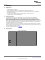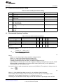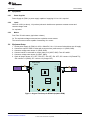
1
User's Guide
SLUU477 – December 2010
800mA, Single-Input, Single Cell Li-Ion Battery Solar
Charger with Power Path
This user's guide describes the features and operation of the bq24210EVM Evaluation Module (EVM). The
EVM assists users in evaluating the bq24210 solar chager. The EVM is also called the HPA678. The
manual includes the bq24210EVM bill of materials, board layout, and schematic.
1
2
3
4
Contents
Introduction .................................................................................................................. 2
1.1
EVM Features ...................................................................................................... 2
1.2
General Description ................................................................................................ 2
1.3
I/O Description ...................................................................................................... 2
1.4
Control and Key Parameters Setting ............................................................................ 3
1.5
Recommendd Operating Conditions ............................................................................ 3
Test Summary ............................................................................................................... 4
2.1
Definitions ........................................................................................................... 4
2.2
Safety ................................................................................................................ 4
2.3
Quality ............................................................................................................... 4
2.4
Apparel .............................................................................................................. 4
2.5
Equipment ........................................................................................................... 5
2.6
Equipment Setup ................................................................................................... 5
2.7
Procedure ........................................................................................................... 6
PCB Layout Guideline ...................................................................................................... 6
Bill of Materials, Board Layout and Schematics ........................................................................ 7
4.1
Bill of Materials ..................................................................................................... 7
4.2
Board Layout ....................................................................................................... 8
4.3
Schematics ........................................................................................................ 11
List of Figures
1
Original Test Setup for HPA678 (bq24210 EVM) ....................................................................... 5
2
Top Assembly ............................................................................................................... 8
3
Top Layer .................................................................................................................... 9
4
Bottom Layer ............................................................................................................... 10
5
bq24210 EVM Schematic
................................................................................................
11
List of Tables
1
I/O Description............................................................................................................... 2
2
Control and Key Parameters Setting ..................................................................................... 3
3
Recommendd Operating Conditions
4
.....................................................................................
Bill of Materials ..............................................................................................................
SLUU477 – December 2010
Submit Documentation Feedback
800mA, Single-Input, Single Cell Li-Ion Battery Solar Charger with Power Path
© 2010, Texas Instruments Incorporated
3
7
1
Introduction
www.ti.com
1
Introduction
1.1
EVM Features
•
•
•
•
•
•
1.2
Evaluation Module for bq24210
800mA, Single-Input, Single Cell Li-Ion Battery Solar Charger with Power Path
Resistor-programmable setting for charge current and input voltage dynamic power management
LED Indication for Status
Test Points for Key Signals Available for Testing Purpose – Easy Probe Hook-up
Jumpers Available – Easy to Change Setting
General Description
The bq24210 series of devices are highly integrated Li-ion linear chargers devices targeted at
space-limited portable applications. The high input voltage range with input overvoltage protection
supports low-cost unregulated adapters. The input voltage regulation loop with programmable input
voltage regulation threshold make it suitable for charging from alternative power sources, such as solar
panel or inductive charging pad. The IC has a single power output that charges the battery. A system load
can be placed in parallel with the battery as long as the average system load does not keep the battery
from charging fully during the 10 hour safety timer.
The battery is charged in three phases: conditioning, constant current and constant voltage. In all charge
phases, an internal control loop monitors the IC junction temperature and reduces the charge current if an
internal temperature threshold is exceeded.
For details, see BQ24210 data sheet (SLUSA76).
1.3
I/O Description
Table 1. I/O Description
2
Jack
Description
J1–VBUS
Positive input
J1–GND
Negative input
J2–BAT
Charger output
J2–GND
Ground
J2–TS
Temperature qualification input
J3-GND
Ground
J3-VDPM
Programs the input voltage regulation threshold
J3-CHG
Charge status indication
J3-EN
Chip enable control
J3-PG
Power present indication
J4-ISET
Programs the fast-charge current setting
J4-VTSB
TS bias reference voltage pin, regulated output
J4-GND
Ground
800mA, Single-Input, Single Cell Li-Ion Battery Solar Charger with Power Path
© 2010, Texas Instruments Incorporated
SLUU477 – December 2010
Submit Documentation Feedback
Introduction
www.ti.com
1.4
Control and Key Parameters Setting
Table 2. Control and Key Parameters Setting
1.5
Jack
Description
Factory Setting
JP1
Programs the fast-charge current setting. 500mA when JP1 ON; external setting
when JP1 OFF
Jumper OFF (external setting)
JP2
Connect /EN and /PG together when JP2 ON to enable charger when power present
Jumper OFF (external /EN)
JP3
Programs the input voltage regulation threshold. 4.5V when JP3 ON; external setting
when JP3 OFF.
Jumper OFF (external setting)
JP4
Limited power charge mode (LPCM) when JP4 ON; normal operation when JP4 OFF Jumper OFF (normal operation)
JP5
Select external TS input or internal TS setting
1-2 : External TS input
2-3 : Internal TS setting
Jumper ON 1-2 (external TS)
JP6
The pull-up power source supplies for the LEDs
1-2 : BAT
2-3 : VBUS
Jumper ON 2-3 (VBUS)
JP7
Charger ON/OFF command
1-2 : OFF
2-3 : ON
Jumper ON 1-2 (charger OFF)
Recommendd Operating Conditions
Table 3. Recommendd Operating Conditions
Description
Min
Max
Unit
Supply voltage, VBUS
Input voltage
4.5
7.3
V
Battery voltage, VBAT
Voltage applied at VBAT terminal of J2
0
4.2
V
Supply current
Maximum input current
0
0.8
A
Charge current, Ichrg
Battery charge current
0
0.8
A
0
125
°C
Operating junction temperature
range, TJ
Typ
Notes
An external resistor is used to program the VBUS_DPM. The programming resistor, RVDPM is dictated by
the following equation:
R VDPM =
(VBUS_ DPM
- VBUS_DPM_ 1
)
KVBUS_DPM
(1)
Where:
VBUS_DPM is the desired input voltage regulation voltage threshold;
VBUS_DPM_1 is the built-in offset threshold, nominally 3.5V
KVBUS_DPM is a gain factor found in the electrical specification.
If VDPM pin is shorted to VSS, the VBUS_DPM should be clamped to 3.65V.
If the VDPM pin is floated (open circuit), the IC operates in Battery Tracking Mode. In this case, VBUS
DPM threshold is internally set as VTRK, which is BAT+100mV (BAT>3.65V) or 3.75V (BAT≤3.4V).
Connecting JP3 set 4.5V VDPM on EVM.
An external resistor is used to program the output current (50-800mA). The equation for charge current is:
K
RISET = ISE T
IO UT
(2)
Where, IOUT is the desired fast charge current; KISET is a gain factor found in the spec.
The termination and pre-charge current are internally set at 10% and 20% of fast charge current
respectively. The pre-charge-to-fast-charge, Vlowv threshold is set to 2.5V.
Connecting JP1 set 500mADC for fast charge current and 100mADC for pre-charge current on EVM.
SLUU477 – December 2010
Submit Documentation Feedback
800mA, Single-Input, Single Cell Li-Ion Battery Solar Charger with Power Path
© 2010, Texas Instruments Incorporated
3
Test Summary
2
Test Summary
2.1
Definitions
www.ti.com
This procedure details how to configure the HPA678 evaluation board. On the test procedure, the
following naming conventions are followed.
VXXX :
LOADW:
V(TPyyy):
V(Jxx):
V(XXX):
External voltage supply name (VBUS, VBAT)
External load name (LOADR, LOADI)
Voltage at internal test point (TPyyy). For example, V(TP1) means the voltage at TP1.
Voltage at jack terminal (Jxx).
Voltage at (XXX). For example, V(VDPM) means the voltage at the test point which is
marked "VDPM".
V(XXX, YYY): Voltage across point XXX and YYY.
I(JXX(YYY)):
Current going out from the YYY terminal of jack XX.
Jxx(BBB):
Terminal or pin BBB of jack xx
Jxx ON :
Internal jumper Jxx terminals are shorted
Jxx OFF:
Internal jumper Jxx terminals are open
Jxx (-YY-) ON: Internal jumper Jxx adjacent terminals marked as "YY" are shorted
Measure:→A,B Check specified parameters A, B. If measured values are not within specified limits the
unit under test has failed.
Observe →A,B Observe if A, B occur. If they do not occur, the unit under test has failed.
Assembly drawings have location for jumpers, test points and individual components
2.2
Safety
1. Safety Glasses are to be worn.
2. This test must be performed by qualified personnel trained in electronics theory and understand the
risks and hazards of the assembly to be tested.
3. ESD precautions must be followed while handling electronic assemblies while performing this test.
4. Precautions should be observed to avoid touching areas of the assembly that may get hot or present a
shock hazard during testing.
2.3
Quality
1. Test data shall be made available upon request by Texas Instruments.
2.4
Apparel
1.
2.
3.
4.
4
Electrostatic smock
Electrostatic Gloves or finger cots
Safety Glasses
Ground ESD wrist strap
800mA, Single-Input, Single Cell Li-Ion Battery Solar Charger with Power Path
© 2010, Texas Instruments Incorporated
SLUU477 – December 2010
Submit Documentation Feedback
Test Summary
www.ti.com
2.5
Equipment
2.5.1
Power Supplies
Power Supply #1 (PS#1): a power supply capable of supplying 20-V at 1-A is required.
2.5.2
Loads
LOAD #1 A 20V (or above), 1A (or above) electronic load that can operate at constant current and
constant voltage mode.
Or: equivalent.
2.5.3
Meters
Four Fluke 75 multi-meters, (equivalent or better)
Or: Two equivalent voltage meters and two equivalent current meters.
The current meters must be capable of measuring 1A+ current.
2.6
Equipment Setup
1.
2.
3.
4.
5.
6.
Set the power supply #1 (PS#1) for 6.5V ± 200mVDC, 1A ± 0.1A current limit and then turn off supply.
Connect the output of PS#1 in series with a current meter (multi-meter) to J1 (VBUS, GND).
Connect a voltage meter across J1 (VBUS, GND).
Connect Load #1 in series with a current meter to J2 (VBAT, GND). Turn off Load #1.
Connect a voltage meter across J2 (VBAT, GND).
Check all jumper shunts. JP1: OFF; JP2: OFF; JP3: OFF; JP4: OFF; JP5: connect 1-2 (External TS);
JP6: connect 2-3 (VBUS); JP7: connect 1-2 (charger OFF).
J1
Power supply
#1
BQ24210 EVM
HPA678
J2
I
Iin
BAT
GND
I
V
GND
VBUS
V
IBAT
Load #1
TS
U1
APPLICATION CIRCUIT
JP3
JP1
LED
PG
CHG
D1
D2
J4
J3
JP4
JP5
JP7
JP6
JP2
Figure 1. Original Test Setup for HPA678 (bq24210 EVM)
SLUU477 – December 2010
Submit Documentation Feedback
800mA, Single-Input, Single Cell Li-Ion Battery Solar Charger with Power Path
© 2010, Texas Instruments Incorporated
5
PCB Layout Guideline
2.7
2.7.1
www.ti.com
Procedure
Power Supply
Make sure EQUIPMENT SETUP steps are followed.
Disconnect LOAD #1. Turn on PS#1.
Measure → V(J1(VBUS)) = 6.5V ± 200mV
Measure → V(J2(VBAT)) = 0V ± 200mV
Measure → V(J4(VTSB)) = 0V ± 200mV
Observe → D1 (PG) ON, D2 (CHG) OFF
2.7.2
Charger Enable and Battery Detection
Connect JP1; Connect 2-3 of JP7 (Charger ON)
Measure → V(J4(VTSB)) = 2.2V ± 300mV
Connect 2-3 of JP5 (Internal TS);
Adjust R6 until V(JP4-1) = 0.7V ± 200mV
Measure → V(J2(VBAT))=4.2V 200mV
Observe → D1 (PG) ON, D2 (CHG) OFF
2.7.3
Charge Current/Voltage Regulation
Reconnect LOAD#1. Turn on. Use the constant voltage mode.
Connect JP1; Set the output voltage to be 2.2V.
Measure → I(J2(VBAT)) = 0.1A ± 50mA
Observe → D1 (PG) ON, D2 (CHG) ON
Increase the voltage of LOAD#1 to be 3.5 V.
Measure → I(J2(VBAT)) = 0.5A ± 100mA
Observe → D1 (PG) ON, D2 (CHG) ON
2.7.4
VDPM ((Input Voltage Regulation) Setting)
Disconnect J3, measure the resistance between J3-1 to GND (6.65kΩ ±10%)
2.7.5
Test Complete
Turn off the power supply and remove all connections from the unit under test (UUT).
3
PCB Layout Guideline
1. It is critical that the exposed thermal pad on the backside of the bq24210 package be soldered to the
PCB ground. Make sure there are sufficient thermal vias right underneath the IC, connecting to the
ground plane on the other layers.
2. Decoupling capacitors for VBUS, BATC should make the interconnections to the IC as short as
possible.
3. Take the EVM layout for design reference.
6
800mA, Single-Input, Single Cell Li-Ion Battery Solar Charger with Power Path
© 2010, Texas Instruments Incorporated
SLUU477 – December 2010
Submit Documentation Feedback
Bill of Materials, Board Layout and Schematics
www.ti.com
4
Bill of Materials, Board Layout and Schematics
4.1
Bill of Materials
Table 4. Bill of Materials
-001
RefDes
Value
Description
SIZE
Part Number
MFR
1
C1
10 µF
Capacitor, Ceramic, 25V,X7R, 10%
1206
STD
STD
2
C2, C4
0.1 µF
Capacitor, Ceramic, 25V, X7R, 10%
0603
STD
STD
1
C3
10 µF
Capacitor, Ceramic, 6.3V, X7R, 10%
0805
STD
STD
0
C5, C6
Open
Capacitor, Ceramic, 25V, X7R, 10%
0603
STD
STD
2
D1, D2
LTST-C190CKT
Diode, LED, Red, 1.8-V, 20-mA, 20-mcd
0603
LTST-C190CKT
Liteon
1
D3
BZX84C5V1-7
Diode, Zener, 5.1V, 350-mW
SOT-23
BZX84C5V1-7
Diodes
1
J1
PEC02SAAN
Header, Male 2-pin, 100mil spacing,
0.100 inch x 2
PEC02SAAN
Sullins
1
J2
ED555/3DS
Terminal Block, 3-pin, 6-A, 3.5mm
0.41 x 0.25 inch
ED555/3DS
OST
1
J3
PEC05SAAN
Header, Male 5-pin, 100mil spacing
0.100 inch x 5
PEC05SAAN
Sullins
1
J4
PEC03SAAN
Header, Male 3-pin, 100mil spacing
0.100 inch x 3
PEC03SAAN
Sullins
4
JP1, JP2,
JP3, JP4
PEC02SAAN
Header, 2-pin, 100mil spacing,
0.100 inch x 2
PEC02SAAN
Sullins
3
JP5, JP6,
JP7
PEC03SAAN
Header, 3 pin, 100mil spacing,
0.100 inch x 3
PEC03SAAN
Sullins
1
R1
21.5k
Resistor, Chip, 1/16W, 1%
0603
STD
STD
2
R2, R4
1.50K
Resistor, Chip, 1/16W, 1%
0603
STD
STD
1
R3
750
Resistor, Chip, 1/16W, 1%
0603
STD
STD
1
R5
6.65k
Resistor, Chip, 1/16W, 1%
0603
Std
Std
1
R6
100k
Potentiometer, 1/4 Cermet, 12-Turn, Top-Adjust
0.25 x 0.17 inch
3266W-1-104LF
Bourns
1
R7
4.75k
Resistor, Chip, 1/16-W, 1%
0603
STD
STD
0
TP1, TP2,
TP3
Open
Test Point, 0.020 Hole
STD
STD
1
U1
BQ24210DCQ
IC, 800mA, Single-Input, Single Cell Li-Ion Battery Solar
Charger with bi-directional Power Path
TDFN-10
BQ24210DCQ
TI
7
—
Shunt, 100-mil, Black
0.1
929950-00
3M
1
—
PCB
HPA678
Any
1
—
Label
THT-13-457-10
Brady
SLUU477 – December 2010
Submit Documentation Feedback
1.25 x 0.25 inch
800mA, Single-Input, Single Cell Li-Ion Battery Solar Charger with Power Path
© 2010, Texas Instruments Incorporated
7
Bill of Materials, Board Layout and Schematics
4.2
www.ti.com
Board Layout
Figure 2. Top Assembly
8
800mA, Single-Input, Single Cell Li-Ion Battery Solar Charger with Power Path
© 2010, Texas Instruments Incorporated
SLUU477 – December 2010
Submit Documentation Feedback
Bill of Materials, Board Layout and Schematics
www.ti.com
Figure 3. Top Layer
SLUU477 – December 2010
Submit Documentation Feedback
800mA, Single-Input, Single Cell Li-Ion Battery Solar Charger with Power Path
© 2010, Texas Instruments Incorporated
9
Bill of Materials, Board Layout and Schematics
www.ti.com
Figure 4. Bottom Layer
10
800mA, Single-Input, Single Cell Li-Ion Battery Solar Charger with Power Path
© 2010, Texas Instruments Incorporated
SLUU477 – December 2010
Submit Documentation Feedback
Bill of Materials, Board Layout and Schematics
www.ti.com
4.3
Schematics
Figure 5. bq24210 EVM Schematic
SLUU477 – December 2010
Submit Documentation Feedback
800mA, Single-Input, Single Cell Li-Ion Battery Solar Charger with Power Path
© 2010, Texas Instruments Incorporated
11
Evaluation Board/Kit Important Notice
Texas Instruments (TI) provides the enclosed product(s) under the following conditions:
This evaluation board/kit is intended for use for ENGINEERING DEVELOPMENT, DEMONSTRATION, OR EVALUATION
PURPOSES ONLY and is not considered by TI to be a finished end-product fit for general consumer use. Persons handling the
product(s) must have electronics training and observe good engineering practice standards. As such, the goods being provided are
not intended to be complete in terms of required design-, marketing-, and/or manufacturing-related protective considerations,
including product safety and environmental measures typically found in end products that incorporate such semiconductor
components or circuit boards. This evaluation board/kit does not fall within the scope of the European Union directives regarding
electromagnetic compatibility, restricted substances (RoHS), recycling (WEEE), FCC, CE or UL, and therefore may not meet the
technical requirements of these directives or other related directives.
Should this evaluation board/kit not meet the specifications indicated in the User’s Guide, the board/kit may be returned within 30
days from the date of delivery for a full refund. THE FOREGOING WARRANTY IS THE EXCLUSIVE WARRANTY MADE BY
SELLER TO BUYER AND IS IN LIEU OF ALL OTHER WARRANTIES, EXPRESSED, IMPLIED, OR STATUTORY, INCLUDING
ANY WARRANTY OF MERCHANTABILITY OR FITNESS FOR ANY PARTICULAR PURPOSE.
The user assumes all responsibility and liability for proper and safe handling of the goods. Further, the user indemnifies TI from all
claims arising from the handling or use of the goods. Due to the open construction of the product, it is the user’s responsibility to
take any and all appropriate precautions with regard to electrostatic discharge.
EXCEPT TO THE EXTENT OF THE INDEMNITY SET FORTH ABOVE, NEITHER PARTY SHALL BE LIABLE TO THE OTHER
FOR ANY INDIRECT, SPECIAL, INCIDENTAL, OR CONSEQUENTIAL DAMAGES.
TI currently deals with a variety of customers for products, and therefore our arrangement with the user is not exclusive.
TI assumes no liability for applications assistance, customer product design, software performance, or infringement of
patents or services described herein.
Please read the User’s Guide and, specifically, the Warnings and Restrictions notice in the User’s Guide prior to handling the
product. This notice contains important safety information about temperatures and voltages. For additional information on TI’s
environmental and/or safety programs, please contact the TI application engineer or visit www.ti.com/esh.
No license is granted under any patent right or other intellectual property right of TI covering or relating to any machine, process, or
combination in which such TI products or services might be or are used.
FCC Warning
This evaluation board/kit is intended for use for ENGINEERING DEVELOPMENT, DEMONSTRATION, OR EVALUATION
PURPOSES ONLY and is not considered by TI to be a finished end-product fit for general consumer use. It generates, uses, and
can radiate radio frequency energy and has not been tested for compliance with the limits of computing devices pursuant to part 15
of FCC rules, which are designed to provide reasonable protection against radio frequency interference. Operation of this
equipment in other environments may cause interference with radio communications, in which case the user at his own expense
will be required to take whatever measures may be required to correct this interference.
EVM Warnings and Restrictions
It is important to operate this EVM within the input voltage range of 4.5 V to 7.3 V and the output voltage range of 0 V to 4.2 V .
Exceeding the specified input range may cause unexpected operation and/or irreversible damage to the EVM. If there are
questions concerning the input range, please contact a TI field representative prior to connecting the input power.
Applying loads outside of the specified output range may result in unintended operation and/or possible permanent damage to the
EVM. Please consult the EVM User's Guide prior to connecting any load to the EVM output. If there is uncertainty as to the load
specification, please contact a TI field representative.
During normal operation, some circuit components may have case temperatures greater than 60°C. The EVM is designed to
operate properly with certain components above 125°C as long as the input and output ranges are maintained. These components
include but are not limited to linear regulators, switching transistors, pass transistors, and current sense resistors. These types of
devices can be identified using the EVM schematic located in the EVM User's Guide. When placing measurement probes near
these devices during operation, please be aware that these devices may be very warm to the touch.
Mailing Address: Texas Instruments, Post Office Box 655303, Dallas, Texas 75265
Copyright © 2010, Texas Instruments Incorporated
IMPORTANT NOTICE
Texas Instruments Incorporated and its subsidiaries (TI) reserve the right to make corrections, modifications, enhancements, improvements,
and other changes to its products and services at any time and to discontinue any product or service without notice. Customers should
obtain the latest relevant information before placing orders and should verify that such information is current and complete. All products are
sold subject to TI’s terms and conditions of sale supplied at the time of order acknowledgment.
TI warrants performance of its hardware products to the specifications applicable at the time of sale in accordance with TI’s standard
warranty. Testing and other quality control techniques are used to the extent TI deems necessary to support this warranty. Except where
mandated by government requirements, testing of all parameters of each product is not necessarily performed.
TI assumes no liability for applications assistance or customer product design. Customers are responsible for their products and
applications using TI components. To minimize the risks associated with customer products and applications, customers should provide
adequate design and operating safeguards.
TI does not warrant or represent that any license, either express or implied, is granted under any TI patent right, copyright, mask work right,
or other TI intellectual property right relating to any combination, machine, or process in which TI products or services are used. Information
published by TI regarding third-party products or services does not constitute a license from TI to use such products or services or a
warranty or endorsement thereof. Use of such information may require a license from a third party under the patents or other intellectual
property of the third party, or a license from TI under the patents or other intellectual property of TI.
Reproduction of TI information in TI data books or data sheets is permissible only if reproduction is without alteration and is accompanied
by all associated warranties, conditions, limitations, and notices. Reproduction of this information with alteration is an unfair and deceptive
business practice. TI is not responsible or liable for such altered documentation. Information of third parties may be subject to additional
restrictions.
Resale of TI products or services with statements different from or beyond the parameters stated by TI for that product or service voids all
express and any implied warranties for the associated TI product or service and is an unfair and deceptive business practice. TI is not
responsible or liable for any such statements.
TI products are not authorized for use in safety-critical applications (such as life support) where a failure of the TI product would reasonably
be expected to cause severe personal injury or death, unless officers of the parties have executed an agreement specifically governing
such use. Buyers represent that they have all necessary expertise in the safety and regulatory ramifications of their applications, and
acknowledge and agree that they are solely responsible for all legal, regulatory and safety-related requirements concerning their products
and any use of TI products in such safety-critical applications, notwithstanding any applications-related information or support that may be
provided by TI. Further, Buyers must fully indemnify TI and its representatives against any damages arising out of the use of TI products in
such safety-critical applications.
TI products are neither designed nor intended for use in military/aerospace applications or environments unless the TI products are
specifically designated by TI as military-grade or "enhanced plastic." Only products designated by TI as military-grade meet military
specifications. Buyers acknowledge and agree that any such use of TI products which TI has not designated as military-grade is solely at
the Buyer's risk, and that they are solely responsible for compliance with all legal and regulatory requirements in connection with such use.
TI products are neither designed nor intended for use in automotive applications or environments unless the specific TI products are
designated by TI as compliant with ISO/TS 16949 requirements. Buyers acknowledge and agree that, if they use any non-designated
products in automotive applications, TI will not be responsible for any failure to meet such requirements.
Following are URLs where you can obtain information on other Texas Instruments products and application solutions:
Products
Applications
Amplifiers
amplifier.ti.com
Audio
www.ti.com/audio
Data Converters
dataconverter.ti.com
Automotive
www.ti.com/automotive
DLP® Products
www.dlp.com
Communications and
Telecom
www.ti.com/communications
DSP
dsp.ti.com
Computers and
Peripherals
www.ti.com/computers
Clocks and Timers
www.ti.com/clocks
Consumer Electronics
www.ti.com/consumer-apps
Interface
interface.ti.com
Energy
www.ti.com/energy
Logic
logic.ti.com
Industrial
www.ti.com/industrial
Power Mgmt
power.ti.com
Medical
www.ti.com/medical
Microcontrollers
microcontroller.ti.com
Security
www.ti.com/security
RFID
www.ti-rfid.com
Space, Avionics &
Defense
www.ti.com/space-avionics-defense
RF/IF and ZigBee® Solutions www.ti.com/lprf
Video and Imaging
www.ti.com/video
Wireless
www.ti.com/wireless-apps
Mailing Address: Texas Instruments, Post Office Box 655303, Dallas, Texas 75265
Copyright © 2010, Texas Instruments Incorporated