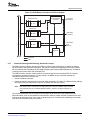
1
TMS320DM647/DM648 DSP
DDR2 Memory Controller
User's Guide
Literature Number: SPRUEK5A
October 2007
2
SPRUEK5A – October 2007
Submit Documentation Feedback
Contents
Preface ............................................................................................................................... 6
1
Introduction................................................................................................................ 9
1.1
Purpose of the Peripheral ....................................................................................... 9
1.2
Features ........................................................................................................... 9
1.3
Functional Block Diagram ....................................................................................... 9
...............................................................
2
Peripheral Architecture ..............................................................................................
2.1
Clock Control ....................................................................................................
2.2
Memory Map ....................................................................................................
2.3
Signal Descriptions .............................................................................................
2.4
Protocol Description(s) .........................................................................................
2.5
Memory Width and Byte Alignment ..........................................................................
2.6
Address Mapping ...............................................................................................
2.7
DDR2 Memory Controller Interface ..........................................................................
2.8
Refresh Scheduling ............................................................................................
2.9
Self-Refresh Mode..............................................................................................
2.10 Reset Considerations ..........................................................................................
2.11 DDR2 SDRAM Memory Initialization .........................................................................
2.12 Interrupt Support ................................................................................................
2.13 EDMA Event Support ..........................................................................................
2.14 Emulation Considerations .....................................................................................
3
Using the DDR2 Memory Controller .............................................................................
3.1
Connecting the DDR2 Memory Controller to DDR2 SDRAM .............................................
3.2
Configuring DDR2 Memory Controller Registers to Meet DDR2 SDRAM Specifications .............
4
DDR2 Memory Controller Registers .............................................................................
4.1
Module ID and Revision Register (MIDR) ...................................................................
4.2
DDR2 Memory Controller Status Register (DMCSTAT) ...................................................
4.3
SDRAM Configuration Register (SDCFG)...................................................................
4.4
SDRAM Refresh Control Register (SDRFC) ................................................................
4.5
SDRAM Timing 1 Register (SDTIM1) ........................................................................
4.6
SDRAM Timing 2 Register (SDTIM2) ........................................................................
4.7
Burst Priority Register (BPRIO) ...............................................................................
4.8
DDR2 Memory Controller Control Register (DMCCTL) ...................................................
Appendix A Revision History .............................................................................................
1.4
Industry Standard(s) Compliance Statement
SPRUEK5A – October 2007
Submit Documentation Feedback
Table of Contents
10
11
11
11
11
13
18
19
22
25
26
26
27
28
28
28
29
29
33
36
37
37
38
40
41
43
44
45
46
3
List of Figures
1
2
3
4
5
6
7
8
9
10
11
12
13
14
15
16
17
18
19
20
21
22
23
24
25
26
27
4
DDR2 Memory Controller Block Diagram ...............................................................................
DDR2 Memory Controller Signals ........................................................................................
DDR2 MRS and EMRS Command ......................................................................................
Refresh Command .........................................................................................................
ACTV Command ...........................................................................................................
DCAB Command ...........................................................................................................
DEAC Command ...........................................................................................................
DDR2 READ Command ...................................................................................................
DDR2 WRT Command ....................................................................................................
Byte Alignment..............................................................................................................
Logical Address-to-DDR2 SDRAM Address Map for 32-Bit SDRAM ...............................................
Logical Address-to-DDR2 SDRAM Address Map for 16-bit SDRAM ................................................
Logical Address-to-DDR2 SDRAM Address Map ......................................................................
DDR2 SDRAM Column, Row, and Bank Access ......................................................................
DDR2 Memory Controller FIFO Block Diagram ........................................................................
DDR2 Memory Controller Reset Block Diagram .......................................................................
Connecting to Two 16-Bit DDR2 SDRAM Devices ....................................................................
Connecting to a Single 16-Bit DDR2 SDRAM Device .................................................................
Connecting to Two 8-Bit DDR2 SDRAM Devices ......................................................................
Module ID and Revision Register (MIDR) ...............................................................................
DDR2 Memory Controller Status Register (DMCSTAT) ..............................................................
SDRAM Configuration Register (SDCFG) ..............................................................................
SDRAM Refresh Control Register (SDRFC)............................................................................
SDRAM Timing 1 Register (SDTIM1) ...................................................................................
SDRAM Timing 2 Register (SDTIM2) ...................................................................................
Burst Priority Register (BPRIO) ..........................................................................................
DDR2 Memory Controller Control Register (DMCCTL) ...............................................................
List of Figures
10
12
14
15
15
16
16
17
18
19
19
20
21
22
23
26
30
31
32
37
37
38
40
41
43
44
45
SPRUEK5A – October 2007
Submit Documentation Feedback
List of Tables
1
2
3
4
5
6
7
8
9
10
11
12
13
14
15
16
17
18
19
20
21
22
23
24
25
A-1
DDR2 Memory Controller Signal Descriptions .........................................................................
DDR2 SDRAM Commands ...............................................................................................
Truth Table for DDR2 SDRAM Commands ............................................................................
Addressable Memory Ranges ............................................................................................
Bank Configuration Register Fields for Address Mapping ............................................................
DDR2 Memory Controller FIFO Description ............................................................................
Refresh Urgency Levels ...................................................................................................
Reset Sources ..............................................................................................................
DDR2 SDRAM Mode Register Configuration ...........................................................................
DDR2 SDRAM Extended Mode Register 1 Configuration ............................................................
SDCFG Configuration .....................................................................................................
DDR2 Memory Refresh Specification ...................................................................................
SDRFC Configuration ......................................................................................................
SDTIM1 Configuration .....................................................................................................
SDTIM2 Configuration .....................................................................................................
DMCCTL Configuration ....................................................................................................
DDR2 Memory Controller Registers .....................................................................................
Module ID and Revision Register (MIDR) Field Descriptions ........................................................
DDR2 Memory Controller Status Register (DMCSTAT) Field Descriptions ........................................
SDRAM Configuration Register (SDCFG) Field Descriptions ........................................................
SDRAM Refresh Control Register (SDRFC) Field Descriptions .....................................................
SDRAM Timing 1 Register (SDTIM1) Field Descriptions .............................................................
SDRAM Timing 2 Register (SDTIM2) Field Descriptions .............................................................
Burst Priority Register (BPRIO) Field Descriptions ....................................................................
DDR2 Memory Controller Control Register (DMCCTL) Field Descriptions .........................................
Document Revision History ...............................................................................................
SPRUEK5A – October 2007
Submit Documentation Feedback
List of Tables
12
13
13
18
19
22
25
26
27
27
33
34
34
34
35
35
36
37
37
38
40
41
43
44
45
46
5
Preface
SPRUEK5A – October 2007
Read This First
About This Manual
This document describes the DDR2 memory controller in the TMS320DM647/DM648 Digital Signal
Processor (DSP).
Notational Conventions
This document uses the following conventions.
• Hexadecimal numbers are shown with the suffix h. For example, the following number is 40
hexadecimal (decimal 64): 40h.
• Registers in this document are shown in figures and described in tables.
– Each register figure shows a rectangle divided into fields that represent the fields of the register.
Each field is labeled with its bit name, its beginning and ending bit numbers above, and its
read/write properties below. A legend explains the notation used for the properties.
– Reserved bits in a register figure designate a bit that is used for future device expansion.
Note:
Acronyms 3PSW, CPSW, CPSW_3G, and 3pGSw are interchangeable and all refer to the 3
port gigabit switch.
Related Documentation From Texas Instruments
The following documents describe the TMS320DM647/DM648 Digital Signal Processor (DSP). Copies of
these documents are available on the Internet at www.ti.com. Tip: Enter the literature number in the
search box provided at www.ti.com.
SPRS372 — TMS320DM647/DM648 Digital Media Processor Data Manual describes the signals,
specifications and electrical characteristics of the device.
SPRU732 — TMS320C64x/C64x+ DSP CPU and Instruction Set Reference Guide describes the CPU
architecture, pipeline, instruction set, and interrupts for the TMS320C64x and TMS320C64x+ digital
signal processors (DSPs) of the TMS320C6000 DSP family. The C64x/C64x+ DSP generation
comprises fixed-point devices in the C6000 DSP platform. The C64x+ DSP is an enhancement of
the C64x DSP with added functionality and an expanded instruction set.
SPRUEK5 — TMS320DM647/DM648 DSP DDR2 Memory Controller User's Guide describes the DDR2
memory controller in the TMS320DM647/DM648 Digital Signal Processor (DSP). The DDR2/mDDR
memory controller is used to interface with JESD79D-2A standard compliant DDR2 SDRAM
devices and standard Mobile DDR SDRAM devices.
SPRUEK6 — TMS320DM647/DM648 DSP External Memory Interface (EMIF) User's Guide describes
the operation of the asynchronous external memory interface (EMIF) in the TMS320DM647/DM648
Digital Signal Processor (DSP). The EMIF supports a glueless interface to a variety of external
devices.
SPRUEK7 — TMS320DM647/DM648 DSP General-Purpose Input/Output (GPIO) User's Guide
describes the general-purpose input/output (GPIO) peripheral in the TMS320DM647/DM648 Digital
Signal Processor (DSP). The GPIO peripheral provides dedicated general-purpose pins that can be
configured as either inputs or outputs. When configured as an input, you can detect the state of the
input by reading the state of an internal register. When configured as an output, you can write to an
internal register to control the state driven on the output pin.
6
Preface
SPRUEK5A – October 2007
Submit Documentation Feedback
www.ti.com
Related Documentation From Texas Instruments
SPRUEK8 — TMS320DM647/DM648 DSP Inter-Integrated Circuit (I2C) Module User's Guide
describes the inter-integrated circuit (I2C) peripheral in the TMS320DM647/DM648 Digital Signal
Processor (DSP). The I2C peripheral provides an interface between the DSP and other devices
compliant with the I2C-bus specification and connected by way of an I2C-bus. External components
attached to this 2-wire serial bus can transmit and receive up to 8-bit wide data to and from the
DSP through the I2C peripheral. This document assumes the reader is familiar with the I2C-bus
specification.
SPRUEL0 — TMS320DM647/DM648 DSP 64-Bit Timer User's Guide describes the operation of the
64-bit timer in the TMS320DM647/DM648 Digital Signal Processor (DSP). The timer can be
configured as a general-purpose 64-bit timer, dual general-purpose 32-bit timers, or a watchdog
timer.
SPRUEL1 — TMS320DM647/DM648 DSP Multichannel Audio Serial Port (McASP) User's Guide
describes the multichannel audio serial port (McASP) in the TMS320DM647/DM648 Digital Signal
Processor (DSP). The McASP functions as a general-purpose audio serial port optimized for the
needs of multichannel audio applications. The McASP is useful for time-division multiplexed (TDM)
stream, Inter-Integrated Sound (I2S) protocols, and intercomponent digital audio interface
transmission (DIT).
SPRUEL2 — TMS320DM647/DM648 DSP Enhanced DMA (EDMA) Controller User's Guide describes
the operation of the enhanced direct memory access (EDMA3) controller in the
TMS320DM647/DM648 Digital Signal Processor (DSP). The EDMA3 controller’s primary purpose is
to service user-programmed data transfers between two memory-mapped slave endpoints on the
DSP.
SPRUEL4 — TMS320DM647/DM648 DSP Peripheral Component Interconnect (PCI) User's Guide
describes the peripheral component interconnect (PCI) port in the TMS320DM647/DM648 Digital
Signal Processor (DSP). The PCI port supports connection of the C642x DSP to a PCI host via the
integrated PCI master/slave bus interface. The PCI port interfaces to the DSP via the enhanced
DMA (EDMA) controller. This architecture allows for both PCI master and slave transactions, while
keeping the EDMA channel resources available for other applications.
SPRUEL5 — TMS320DM647/DM648 DSP Host Port Interface (UHPI) User's Guide describes the host
port interface (HPI) in the TMS320DM647/DM648 Digital Signal Processor (DSP). The HPI is a
parallel port through which a host processor can directly access the CPU memory space. The host
device functions as a master to the interface, which increases ease of access. The host and CPU
can exchange information via internal or external memory. The host also has direct access to
memory-mapped peripherals. Connectivity to the CPU memory space is provided through the
enhanced direct memory access (EDMA) controller.
SPRUEL8 — TMS320DM647/DM648 DSP Universal Asynchronous Receiver/Transmitter (UART)
User's Guide describes the universal asynchronous receiver/transmitter (UART) peripheral in the
TMS320DM647/DM648 Digital Signal Processor (DSP). The UART peripheral performs
serial-to-parallel conversion on data received from a peripheral device, and parallel-to-serial
conversion on data received from the CPU.
SPRUEL9 — TMS320DM647/DM648 DSP VLYNQ Port User's Guide describes the VLYNQ port in the
TMS320DM647/DM648 Digital Signal Processor (DSP). The VLYNQ port is a high-speed
point-to-point serial interface for connecting to host processors and other VLYNQ compatible
devices. It is a full-duplex serial bus where transmit and receive operations occur separately and
simultaneously without interference.
SPRUEM1 — TMS320DM647/DM648 DSP Video Port/VCXO Interpolated Control (VIC) Port User's
Guide discusses the video port and VCXO interpolated control (VIC) port in the
TMS320DM647/DM648 Digital Signal Processor (DSP). The video port can operate as a video
capture port, video display port, or transport channel interface (TCI) capture port. The VIC port
provides single-bit interpolated VCXO control with resolution from 9 bits to up to 16 bits. When the
video port is used in TCI mode, the VIC port is used to control the system clock, VCXO, for MPEG
transport channel.
SPRUEK5A – October 2007
Submit Documentation Feedback
Read This First
7
www.ti.com
Related Documentation From Texas Instruments
SPRUEM2 — TMS320DM647/DM648 DSP Serial Port Interface (SPI) User's Guide discusses the Serial
Port Interface (SPI) in the TMS320DM647/DM648 Digital Signal Processor (DSP). This reference
guide provides the specifications for a 16-bit configurable, synchronous serial peripheral interface.
The SPI is a programmable-length shift register, used for high speed communication between
external peripherals or other DSPs.
SPRUEU6 — TMS320DM647/DM648 DSP Subsystem User's Guide describes the subsystem in the
TMS320DM647/DM648 Digital Signal Processor (DSP). The subsystem is responsible for
performing digital signal processing for digital media applications. The subsystem acts as the
overall system controller, responsible for handling many system functions such as system-level
initialization, configuration, user interface, user command execution, connectivity functions, and
overall system control.
SPRUF57 — TMS320DM647/DM648 DSP 3 Port Switch (3PSW) Ethernet Subsystem User's Guide
describes the operation of the 3 port switch (3PSW) ethernet subsystem in the
TMS320DM647/DM648 Digital Signal Processor (DSP). The 3 port switch gigabit ethernet
subsystem provides ethernet packet communication and can be configured as an ethernet switch
(DM648 only). It provides the serial gigabit media independent interface (SGMII), the management
data input output (MDIO) for physical layer device (PHY) management.
Trademarks
8
Read This First
SPRUEK5A – October 2007
Submit Documentation Feedback
User's Guide
SPRUEK5A – October 2007
DSP DDR2 Memory Controller
1
Introduction
This document describes the DDR2 memory controller in the device.
1.1
Purpose of the Peripheral
The DDR2 memory controller is used to interface with JESD79D-2A standard compliant DDR2 SDRAM
devices. Memory types such as DDR1 SDRAM, SDR SDRAM, SBSRAM, and asynchronous memories
are not supported. The DDR2 memory controller SDRAM can be used for program and data storage.
1.2
Features
The DDR2 memory controller supports the following features:
• JESD79D-2A standard compliant DDR2 SDRAM
• 256 Mbyte memory space
• Data bus width of 32 or 16 bits
• CAS latencies: 2, 3, 4, and 5
• Internal banks: 1, 2, 4, and 8
• Burst length: 8
• Burst type: sequential
• 1 CE signal
• Page sizes: 256, 512, 1024, and 2048
• SDRAM auto-initialization
• Self-refresh mode
• Prioritized refresh
• Programmable refresh rate and backlog counter
• Programmable timing parameters
1.3
Functional Block Diagram
The DDR2 memory controller is the main interface to external DDR2 memory (see Figure 1). Master
peripherals, such as the EDMA controller and the CPU can access the DDR2 memory controller through
the switched central resource (SCR). The DDR2 memory controller performs all memory-related
background tasks such as opening and closing banks, refreshes, and command arbitration.
SPRUEK5A – October 2007
Submit Documentation Feedback
DSP DDR2 Memory Controller
9
www.ti.com
Introduction
Figure 1. DDR2 Memory Controller Block Diagram
L1P
cache/SRAM
EMIFA
PLL2
Switched central resource
DDR2 memory
controller
L1 program memory controller
Cache
control
Bandwidth
management
C64x+ CPU
Memory
protection
Instruction fetch
SPLOOP buffer
16/32−bit instruction dispatch
Instruction decode
IDMA
External
memory
controller
Master
DMA
Slave
DMA
EDMA
controller
Advanced
event
triggering
(AET)
Cache control
Bandwidth management
Memory protection
Configuration
registers
Other
peripherals
Boot
configuration
L2 memory
L2 memory
controller
Data path A
L1
S1
M1
Data path B
D1
Register file A
L1 data memory controller
Cache control
Memory protection
Bandwidth management
D2
M2
S2
L2
Register file B
Interrupt
and exception
controller
Power control
PLL2
L1D
cache/SRAM
1.4
Industry Standard(s) Compliance Statement
The DDR2 memory controller is compliant with the JESD79D-2A DDR2 SDRAM standard with the
exception of the On Die Termination (ODT) feature. The DSP does not include any on-die terminating
resistors. Furthermore, the on-die terminating resistors of the DDR2 SDRAM device must be disabled by
tying the ODT input pin of the DDR2 SDRAM memory to ground.
10
DSP DDR2 Memory Controller
SPRUEK5A – October 2007
Submit Documentation Feedback
www.ti.com
Peripheral Architecture
2
Peripheral Architecture
The DDR2 memory controller can gluelessly interface to most standard DDR2 SDRAM devices and
supports such features as self-refresh mode and prioritized refresh. In addition, it provides flexibility
through programmable parameters such as the refresh rate, CAS latency, and many SDRAM timing
parameters.
The following sections describe the architecture of the DDR2 memory controller as well as how to
interface and configure it to perform read and write operations to DDR2 SDRAM devices. Also, Section 3
provides a detailed example of interfacing the DDR2 memory controller to a common DDR2 SDRAM
device.
2.1
Clock Control
The DDR2 memory controller is clocked directly from the output of the second phase-locked loop (PLL2)
of the device. The PLL2 multiplies its input clock by 20. This clock is divided by 2 to generate DDR_CLK.
The frequency of DDR_CLK can be determined by using the following formula:
DDR_CLK frequency = (PLL2 input clock frequency×20)/2 = PLL2 input clock frequency×10
The second output clock of the DDR2 memory controller, DDR_CLK, is the inverse of DDR_CLK. For
more information on the PLL2, see the device-specific data manual.
2.2
Memory Map
Please see the device-specific data manual for information describing the device memory map.
2.3
Signal Descriptions
The DDR2 memory controller signals are shown in Figure 2 and described in Table 1. The following
features are included:
•
•
•
•
•
•
The maximum width for the data bus (DDR_D[31:0]) is 32-bits.
The address bus (DDR_A[13:0]) is 14-bits wide with an additional 3 bank address pins (DDR_BA[2:0]).
Two differential output clocks (DDR_CLK and DDR_CLK) driven by internal clock sources.
Command signals: Row and column address strobe (DDR_RAS and DDR_CAS), write enable strobe
(DDR_WE), data strobe (DDR_DQS[3:0] and DDR_DQS[3:0]), and data mask (DDR_DQM[3:0]).
One chip select signal (DDR_CS) and one clock enable signal (DDR_CKE).
Two on-die termination output signals (DDR_ODT[1:0]).
SPRUEK5A – October 2007
Submit Documentation Feedback
DSP DDR2 Memory Controller
11
www.ti.com
Peripheral Architecture
Figure 2. DDR2 Memory Controller Signals
DDR_CLK
DDR_CLK
DDR_CKE
DDR_CS
DDR_WE
DDR_RAS
DDR2
memory
controller
DDR_CAS
DDR_DQM[3:0]
DDR_DQS[3:0]
DDR_DQS[3:0]
DDR_BA[2:0]
DDR_A[13:0]
DDR_D[31:0]
DDR_ODT[1:0]
DDR_DQGATE[3:0]
DDR_VREF
Table 1. DDR2 Memory Controller Signal Descriptions
12
Pin
Description
DDR_D[31:0]
Bidirectional data bus. Input for data reads and output for data writes.
DDR_A[13:0]
External address output.
DDR_CS
Active-low chip enable for memory space CE0. DDR_CS is used to enable the DDR2 SDRAM memory
device during external memory accesses. DDR_CS pin stays low throughout the operation of the DDR2
memory controller; it never goes high. Note that this behavior does not affect the ability of the DDR2 memory
controller to access DDR2 SDRAM memory devices.
DDR_DQM[3:0]
Active-low output data mask.
DDR_CLK/
DDR_CLK
Differential clock outputs.
DDR_CKE
Clock enable (used for self-refresh mode).
DDR_CAS
Active-low column address strobe.
DDR_RAS
Active-low row address strobe.
DDR_WE
Active-low write enable.
DDR_DQS[3:0]/
DDR_DQS[3:0]
Differential data strobe bidirectional signals.
DDR_ODT[1:0]
On-die termination signals to external DDR2 SDRAM. These pins are reserved for future use and should not
be connected to the DDR2 SDRAM. Note: there are no on-die termination resistors implemented on the die
of this device.
DDR_BA[2:0]
Bank-address control outputs.
DDR_DQGATE[3:0]
Data strobe gate pins. These pins are used as a timing reference during memory reads. The
DDR_DQGATE0 and DDR_DQGATE2 pins should be routed out and connected to the DDR_DQGATE1 and
DDR_DQGATE3 pins, respectively. For more routing requirements on these pins, see the device-specific
data manual.
DDR_VREF
DDR2 Memory Controller reference voltage. This voltage must be supplied externally. See the
device-specific data manual for more details.
DSP DDR2 Memory Controller
SPRUEK5A – October 2007
Submit Documentation Feedback
www.ti.com
Peripheral Architecture
2.4
Protocol Description(s)
The DDR2 memory controller supports the DDR2 SDRAM commands listed in Table 2. Table 3 shows the
signal truth table for the DDR2 SDRAM commands.
Table 2. DDR2 SDRAM Commands
Command
Function
ACTV
Activates the selected bank and row.
DCAB
Precharge all command. Deactivates (precharges) all banks.
DEAC
Precharge single command. Deactivates (precharges) a single bank.
DESEL
Device Deselect.
EMRS
Extended Mode Register set. Allows altering the contents of the mode register.
MRS
Mode register set. Allows altering the contents of the mode register.
NOP
No operation.
Power Down
Power down mode.
READ
Inputs the starting column address and begins the read operation.
READ with
autoprecharge
Inputs the starting column address and begins the read operation. The read operation is followed by a
precharge.
REFR
Autorefresh cycle.
SLFREFR
Self-refresh mode.
WRT
Inputs the starting column address and begins the write operation.
WRT with
autoprecharge
Inputs the starting column address and begins the write operation. The write operation is followed by a
precharge.
Table 3. Truth Table for DDR2 SDRAM Commands
DDR2 SDRAM
Signals
CKE
CS
RAS
CAS
WE
BA[2:0]
A[13:11, 9:0]
A10
DDR_A[13:11, 9:0]
DDR_A[10]
DDR_CKE
DDR2 Memory
Controller Signals
Previous
Cycles
Current Cycle
DDR_CS
DDR_RAS
DDR_CAS
DDR_WE
DDR_BA[2:0
]
ACTV
H (1)
H
L
L
H
H
Bank
DCAB
H
H
L
L
H
L
X
X
DEAC
H
H
L
L
H
L
Bank
X
MRS
H
H
L
L
L
L
BA (2)
EMRS
H
H
L
L
L
L
BA
READ
H
H
L
H
L
H
BA
Column Address
L
READ with
precharge
H
H
L
H
L
H
BA
Column Address
H
WRT
H
H
L
H
L
L
BA
Column Address
L
WRT with precharge
H
H
L
H
L
L
BA
Column Address
L
REFR
H
H
L
L
L
H
X
X
X
SLFREFR
entry
H
L
L
L
L
H
X
X
X
SLFREFR
exit
L
H
H
X
X
X
X
X
X
L
H
H
H
X
X
X
NOP
H
X
L
H
H
H
X
X
X
DESEL
H
X
H
X
X
X
X
X
X
Power Down entry
H
L
H
X
X
X
X
X
X
L
H
H
H
X
X
X
H
X
X
X
X
X
X
L
H
H
H
X
X
X
Power Down exit
(1)
(2)
L
H
Row Address
L
L
OP Code
OP Code
Legend: H means logic high; L means logic low; X means don't care (either H or L).
BA refers to the bank address pins (BA[2:0]).
SPRUEK5A – October 2007
Submit Documentation Feedback
DSP DDR2 Memory Controller
13
www.ti.com
Peripheral Architecture
2.4.1
Mode Register Set (MRS and EMRS)
DDR2 SDRAM contains mode and extended mode registers that configure the DDR2 memory for
operation. These registers control burst type, burst length, CAS latency, DLL enable/disable, single-ended
strobe, etc.
The DDR2 memory controller programs the mode and extended mode registers of the DDR2 memory by
issuing MRS and EMRS commands. When the MRS or EMRS command is executed, the value on
DDR_BA[1:0] selects the mode register to be written and the data on DDR_A[12:0] is loaded into the
register. Figure 3 shows the timing for an MRS and EMRS command.
The DDR2 memory controller only issues MRS and EMRS commands during the DDR2 memory controller
initialization sequence. See Section 2.11 for more information.
Figure 3. DDR2 MRS and EMRS Command
MRS/EMRS
DDR_CLK
DDR_CLK
DDR_CKE
DDR_CS
DDR_RAS
DDR_CAS
DDR_WE
2.4.2
DDR_A[13:0]
COL
DDR_BA[2:0]
BANK
Refresh Mode
The DDR2 memory controller issues refresh commands to the DDR2 SDRAM device (Figure 4). REFR is
automatically preceded by a DCAB command, ensuring the deactivation of all CE spaces and banks
selected. Following the DCAB command, the DDR2 memory controller begins performing refreshes at a
rate defined by the refresh rate (REFRESH_RATE) bit in the SDRAM refresh control register (SDRFC).
Page information is always invalid before and after a REFR command; thus, a refresh cycle always forces
a page miss. This type of refresh cycle is often called autorefresh. Autorefresh commands may not be
disabled within the DDR2 memory controller. See Section 2.8 for more details on REFR command
scheduling.
14
DSP DDR2 Memory Controller
SPRUEK5A – October 2007
Submit Documentation Feedback
www.ti.com
Peripheral Architecture
Figure 4. Refresh Command
DDR_CLK
DDR_CLK
REFR
DDR_CKE
DDR_CS
DDR_RAS
DDR_CAS
DDR_WE
DDR_A[13:0]
DDR_BA[2:0]
DDR_DQM[3:0]
2.4.3
Activation (ACTV)
The DDR2 memory controller automatically issues the activate (ACTV) command before a read or write to
a closed row of memory. The ACTV command opens a row of memory, allowing future accesses (reads or
writes) with minimum latency. The value of DDR_BA[2:0] selects the bank and the value of A[12:0] selects
the row. When the DDR2 memory controller issues an ACTV command, a delay of tRCD is incurred before
a read or write command is issued. Figure 5 shows an example of an ACTV command. Reads or writes to
the currently active row and bank of memory can achieve much higher throughput than reads or writes to
random areas because every time a new row is accessed, the ACTV command must be issued and a
delay of tRCD incurred.
Figure 5. ACTV Command
ACTV
DDR_CLK
DDR_CLK
DDR_CKE
DDR_CS
DDR_RAS
DDR_CAS
DDR_WE
DDR_A[13:0]
ROW
DDR_BA[2:0]
BANK
DDR_DQM[3:0]
SPRUEK5A – October 2007
Submit Documentation Feedback
DSP DDR2 Memory Controller
15
www.ti.com
Peripheral Architecture
2.4.4
Deactivation (DCAB and DEAC)
The precharge all banks command (DCAB) is performed after a reset to the DDR2 memory controller or
following the initialization sequence. DDR2 SDRAMs also require this cycle prior to a refresh (REFR) and
mode set register commands (MRS and EMRS). During a DCAB command, DDR_A[10] is driven high to
ensure the deactivation of all banks. Figure 6 shows the timing diagram for a DCAB command.
Figure 6. DCAB Command
DCAB
DDR_CLK
DDR_CLK
DDR_CKE
DDR_CS
DDR_RAS
DDR_CAS
DDR_WE
DDR_A[13:11, 9:0]
DDR_A[10]
DDR_BA[2:0]
DDR_DQM[3:0]
The DEAC command closes a single bank of memory specified by the bank select signals. Figure 7 shows
the timings diagram for a DEAC command.
Figure 7. DEAC Command
DEAC
DDR_CLK
DDR_CLK
DDR_CKE
DDR_CS
DDR_RAS
DDR_CAS
DDR_WE
DDR_A[13:11, 9:0]
DDR_A[10]
DDR_BA[2:0]
DDR_DQM[3:0]
16
DSP DDR2 Memory Controller
SPRUEK5A – October 2007
Submit Documentation Feedback
www.ti.com
Peripheral Architecture
2.4.5
READ Command
Figure 8 shows the DDR2 memory controller performing a read burst from DDR2 SDRAM. The READ
command initiates a burst read operation to an active row. During the READ command, DDR_CAS drives
low, DDR_WE and DDR_RAS remain high, the column address is driven on DDR_A[12:0], and the bank
address is driven on DDR_BA[2:0].
The DDR2 memory controller uses a burst length of 8, and has a programmable CAS latency of 2, 3, 4, or
5. The CAS latency is three cycles in Figure 8. Read latency is equal to CAS latency plus additive latency.
The DDR2 memory controller always configures the memory to have an additive latency of 0, so read
latency equals CAS latency. Since the default burst size is 8, the DDR2 memory controller returns 8
pieces of data for every read command. If additional accesses are not pending to the DDR2 memory
controller, the read burst completes and the unneeded data is disregarded. If additional accesses are
pending, depending on the scheduling result, the DDR2 memory controller can terminate the read burst
and start a new read burst. Furthermore, the DDR2 memory controller does not issue a DCAB/DEAC
command until page information becomes invalid.
Figure 8. DDR2 READ Command
DDR_CLK
DDR_CLK
DDR_CKE
DDR_CS
DDR_RAS
DDR_CAS
DDR_WE
DDR_A[13:0]
DDR_BA[2:0]
COL
BANK
DDR_A[10]
DDR_DQM[3:0]
CAS Latency
DDR_D[31:0]
D0
D1
D2
D3
D4
D5
D6
D7
DDR_DQS[3:0]
SPRUEK5A – October 2007
Submit Documentation Feedback
DSP DDR2 Memory Controller
17
www.ti.com
Peripheral Architecture
2.4.6
Write (WRT) Command
Prior to a WRT command, the desired bank and row are activated by the ACTV command. Following the
WRT command, a write latency is incurred. Write latency is equal to CAS latency minus 1. All writes have
a burst length of 8. The use of the DDR_DQM outputs allows byte and halfword writes to be executed.
Figure 9 shows the timing for a write on the DDR2 memory controller.
If the transfer request is for less than 8 words, depending on the scheduling result and the pending
commands, the DDR2 memory controller can:
• Mask out the additional data using DDR_DQM outputs
• Terminate the write burst and start a new write burst
The DDR2 memory controller does not perform the DEAC command until page information becomes
invalid.
Figure 9. DDR2 WRT Command
DDR_CLK
DDR_CLK
Sample
Write Latency
DDR_CKE
DDR_CS
DDR_RAS
DDR_CAS
DDR_WE
DDR_A[13:0]
DDR_BA[2:0]
COL
BANK
DDR_A[10]
DDR_DQM[3:0]
DQM1 DQM2 DQM3 DQM4 DQM5 DQM6 DQM7 DQM8
DDR_D[31:0]
D0
D1
D2
D3
D4
D5
D6
D7
DDR_DQS[3:0]
2.5
Memory Width and Byte Alignment
The DDR2 memory controller supports memory widths of 16 bits and 32 bits. Table 4 summarizes the
addressable memory ranges on the DDR2 memory controller.
Table 4. Addressable Memory Ranges
18
Memory Width
Maximum Addressable Bytes
Address Type Generated by DDR2
Memory Controller
×16
128 Mbytes
Halfword address
×32
256 Mbytes
Word address
DSP DDR2 Memory Controller
SPRUEK5A – October 2007
Submit Documentation Feedback
www.ti.com
Peripheral Architecture
Figure 10 shows the byte lanes used on the DDR2 memory controller. The external memory is always
right aligned on the data bus.
Figure 10. Byte Alignment
DDR2 memory controller data bus
DDR_D[23:16]
(Byte Lane 2)
DDR_D[31:24]
(Byte Lane 3)
DDR_D[15:8]
(Byte Lane 1)
DDR_D[7:0]
(Byte Lane 0)
32-bit memory device
16-bit memory device
2.6
Address Mapping
The DDR2 memory controller views external DDR2 SDRAM as one continuous block of memory. This
statement is true regardless of the number of memory devices located on the chip select space. The
DDR2 memory controller receives DDR2 memory access requests along with a 32-bit logical address from
the rest of the system. In turn, DDR2 memory controller uses the logical address to generate a row/page,
column, and bank address for the DDR2 SDRAM. The number of column and bank address bits used is
determined by the IBANK and PAGESIZE fields (see Table 5). The DDR2 memory controller uses up to
14 bits for the row/page address.
Table 5. Bank Configuration Register Fields for Address Mapping
Bit Field
Bit Value Bit Description
IBANK
Defines the number of internal banks on the external DDR2 memory.
0
1 bank
1h
2 banks
2h
4 banks
3h
8 banks
PAGESIZE
Defines the page size of each page of the external DDR2 memory.
0
256 words (requires 8 column address bits)
1h
512 words (requires 9 column address bits)
2h
1024 words (requires 10 column address bits)
3h
2048 words (requires 11 column address bits)
Figure 11 and Figure 12 show how the logical address bits map to the row, column, and bank bits all
combinations of IBANK and PAGESIZE values. Note that the upper four bits of the logical address cannot
be used for memory addressing, as the DDR2 memory controller has a maximum addressable memory
range of 256 Mbytes.
The DDR2 memory controller address pins provide the row and column address to the DDR2 SDRAM,
thus the DDR2 memory controller appropriately shifts the logical address during row and column address
selection. The bank address is driven to the DDR2 SDRAM using the bank address pins. The two lower
bits of the logical address decode the value of the byte enable pins (only used for accesses less than the
width of the DDR2 memory controller data bus).
Figure 11. Logical Address-to-DDR2 SDRAM Address Map for 32-Bit SDRAM
SPRUEK5A – October 2007
Submit Documentation Feedback
DSP DDR2 Memory Controller
19
www.ti.com
Peripheral Architecture
SDCFG Bit
Logical Address
IBANK
PAGESIZE
31:28
27
26
25
24
0
0
X
X
X
X
X
1
0
X
X
X
X
2
0
X
X
X
3
0
X
X
0
1
X
X
X
1
1
X
X
X
2
1
X
X
3
1
X
0
2
X
X
1
2
X
X
2
2
X
3
2
X
0
3
X
1
3
X
2
3
X
3
3
X
(1)
23
22:17
16
15
14
13
12
11
10
9:2
nrb=14 (1)
ncb=8
nrb=14
nbb=1
nrb=14
nrb=14
ncb=8
nbb=3
X
ncb=8
nrb=14
ncb=9
nrb=14
nbb=1
nrb=14
ncb=9
nbb=2
nrb=14
ncb=9
nbb=3
X
ncb=9
nrb=14
ncb=10
nrb=14
nbb=1
nrb=14
ncb=10
nbb=2
nrb=13
ncb=10
nbb=3
X
ncb=8
nbb=2
ncb=10
nrb=14
ncb=11
nrb=14
nbb=1
nrb=12
ncb=11
nbb=2
nrb=11
ncb=11
nbb=3
ncb=11
Legend: nrb = number of row address bits; ncb = number of column address bits; nbb = number of bank address bits; BE = byte
enable bits.
Figure 12. Logical Address-to-DDR2 SDRAM Address Map for 16-bit SDRAM
SDCFG Bit
PAGESIZE
31:28
27
26
25
24
23
0
0
X
X
X
X
X
X
1
0
X
X
X
X
X
2
0
X
X
X
X
3
0
X
X
X
0
1
X
X
X
X
1
1
X
X
X
X
2
1
X
X
X
3
1
X
X
0
2
X
X
X
1
2
X
X
X
2
2
X
X
3
2
X
0
3
X
X
1
3
X
X
2
3
X
3
3
X
(1)
20
Logical Address
IBANK
22
21:16
15
14
13
12
11
10
9
ncb=8
nrb=14
nbb=1
nrb=14
nbb=2
nrb=14
X
ncb=8
ncb=9
nrb=14
nbb=1
nrb=14
ncb=9
ncb=10
nrb=14
nbb=1
nrb=14
nbb=2
nrb=14
nbb=3
nrb=14
ncb=10
ncb=10
ncb=10
ncb=11
nrb=14
nrb=12
ncb=9
nbb=3
nrb=14
X
ncb=9
nbb=2
nrb=14
X
ncb=8
ncb=8
nbb=3
nrb=14
nrb=13
8:1
nrb=14 (1)
nbb=1
nbb=2
nbb=3
ncb=11
ncb=11
ncb=11
Legend: nrb = number of row address bits; ncb = number of column address bits; nbb = number of bank address bits; BE = byte
enable bit.
DSP DDR2 Memory Controller
SPRUEK5A – October 2007
Submit Documentation Feedback
www.ti.com
Peripheral Architecture
Figure 11 shows how the DSP memory map is partitioned into columns, rows, and banks. Note that during
a linear access, the DDR2 memory controller increments the column address as the logical address
increments. When the DDR2 memory controller reaches a page/row boundary, it moves onto the same
page/row in the next bank. This movement continues until the same page has been accessed in all banks.
To the DDR2 SDRAM, this process looks as shown on Figure 14.
By traversing across banks while remaining on the same row/page, the DDR2 memory controller
maximizes the number of activated banks for a linear access. This results in the maximum number of
open pages when performing a linear access being equal to the number of banks. Note that the DDR2
memory controller never opens more than one page per bank.
Ending the current access is not a condition that forces the active DDR2 SDRAM row/page to be closed.
The DDR2 memory controller leaves the active row open until it becomes necessary to close it. This
decreases the deactivate-reactivate overhead.
Figure 13. Logical Address-to-DDR2 SDRAM Address Map
Col. 0
Col. 1
Col. 2
Col. 3
Col. 4
Col. M−1
Col. M
Row 0, bank 0
Row 0, bank 1
Row 0, bank 2
Row 0, bank P
Row 1, bank 0
Row 1, bank 1
Row 1, bank 2
Row 1, bank P
Row N, bank 0
Row N, bank 1
Row N, bank 2
Row N, bank P
A
M is number of columns (as determined by PAGESIZE) minus 1, P is number of banks (as determined by IBANK)
minus 1, and N is number of rows (as determined by both PAGESIZE and IBANK) minus 1.
SPRUEK5A – October 2007
Submit Documentation Feedback
DSP DDR2 Memory Controller
21
www.ti.com
Peripheral Architecture
Figure 14. DDR2 SDRAM Column, Row, and Bank Access
Bank 0
C C C
o o o
l l l
0 1 2 3
C
o
l
M
Row 0
Row 1
Row 2
Bank 1
Row 0
C C C
o o o
l l l
0 1 2 3
Row 1
Row 2
C
o
l
M
Bank 2
Row 0
Row 1
Row 2
C C C
o o o
l l l
0 1 2 3
C
o
l
M
Bank P
Row 0
Row 1
Row N
C C C
o o o
l l l
0 1 2 3
C
o
l
M
Row 2
Row N
Row N
Row N
A
2.7
M is number of columns (as determined by PAGESIZE) minus 1, P is number of banks (as determined by IBANK)
minus 1, and N is number of rows (as determined by both PAGESIZE and IBANK) minus 1.
DDR2 Memory Controller Interface
To move data efficiently from on-chip resources to external DDR2 SDRAM device, the DDR2 memory
controller makes use of a command FIFO, a write FIFO, a read FIFO, and command and data schedulers.
Table 6 describes the purpose of each FIFO.
Figure 15 shows the block diagram of the DDR2 memory controller FIFOs. Commands, write data, and
read data arrive at the DDR2 memory controller parallel to each other. The same peripheral bus is used to
write and read data from external memory as well as internal memory-mapped registers.
Table 6. DDR2 Memory Controller FIFO Description
22
Depth (64-Bit
Doublewords)
FIFO
Description
Command
Stores all commands coming from on-chip requesters
7
Write
Stores write data coming from on-chip requesters to
memory
11
Read
Stores read data coming from memory to on-chip
requesters
17
DSP DDR2 Memory Controller
SPRUEK5A – October 2007
Submit Documentation Feedback
www.ti.com
Peripheral Architecture
Figure 15. DDR2 Memory Controller FIFO Block Diagram
Command FIFO
Command/Data
Scheduler
Command
to Memory
EDMA BUS
Write FIFO
Write Data
to Memory
Read FIFO
Read Data
from
Memory
Registers
Command
Data
2.7.1
Command Ordering and Scheduling, Advanced Concept
The DDR2 memory controller performs command re-ordering and scheduling in an attempt to achieve
efficient transfers with maximum throughput. The goal is to maximize the utilization of the data, address,
and command buses while hiding the overhead of opening and closing DDR2 SDRAM rows. Command
re-ordering takes place within the command FIFO.
The DDR2 memory controller examines all the commands stored in the command FIFO to schedule
commands to the external memory. For each master, the DDR2 memory controller reorders the
commands based on the following rules:
• Selects the oldest command
• A read command is advanced before an older write command if the read is to a different block address
(2048 bytes) and the read priority is equal to or greater than the write priority.
Note:
Most masters issue commands on a single priority level. Also, the EDMA transfer controller
read and write ports are considered different masters, and thus, the above rule does not
apply.
The second bullet above may be viewed as an exception to the first bullet. This means that for an
individual master, all of its commands will complete from oldest to newest, with the exception that a read
may be advanced ahead of an older, lower or equal priority write. Following this scheduling, each master
may have one command ready for execution.
SPRUEK5A – October 2007
Submit Documentation Feedback
DSP DDR2 Memory Controller
23
www.ti.com
Peripheral Architecture
Next, the DDR2 memory controller examines each of the commands selected by the individual masters
and performs the following reordering:
• Among all pending reads, selects reads to rows already open. Among all pending writes, selects writes
to rows already open.
• Selects the highest priority command from pending reads and writes to open rows. If multiple
commands have the highest priority, then the DDR2 memory controller selects the oldest command.
The DDR2 memory controller may now have a final read and write command. If the Read FIFO is not full,
then the read command will be performed before the write command, otherwise the write command will be
performed first.
Besides commands received from on-chip resources, the DDR2 memory controller also issues refresh
commands. The DDR2 memory controller attempts to delay refresh commands as long as possible to
maximize performance while meeting the SDRAM refresh requirements. As the DDR2 memory controller
issues read, write, and refresh commands to DDR2 SDRAM device, it follows the following priority
scheme:
1. (Highest) Refresh request resulting from the Refresh Must level of urgency (see Section 2.8) being
reached
2. Read request without a higher priority write (selected from above reordering algorithm)
3. Refresh request resulting from the Refresh Need level of urgency (see Section 2.8) being reached
4. Write request (selected from above reordering algorithm)
5. Refresh request resulting from Refresh May level of urgency (see Section 2.8) being reached
6. (Lowest) Request to enter self-refresh mode
The following results from the above scheduling algorithm:
• All writes from a single master will complete in order
• All reads from a single master will complete in order
• From the same master, any read to the same location (or within 2048 bytes) as a previous write will
complete in order
2.7.2
Command Starvation
The reordering and scheduling rules listed above may lead to command starvation, which is the
prevention of certain commands from being processed by the DDR2 memory controller. Command
starvation results from the following conditions:
• A continuous stream of high-priority read commands can block a low-priority write command
• A continuous stream of DDR2 SDRAM commands to a row in an open bank can block commands to
the closed row in the same bank.
To avoid these conditions, the DDR2 memory controller can momentarily raise the priority of the oldest
command in the command FIFO after a set number of transfers have been made. The PRIO_RAISE field
in the Burst Priority Register (BPRIO) sets the number of the transfers that must be made before the
DDR2 memory controller will raise the priority of the oldest command.
Note:
24
Leaving the PRIO_RAISE bits at their default value (FFh) disables this feature of the DDR2
memory controller. This means commands can stay in the command FIFO indefinitely.
Therefore, these bits should be set to FEh immediately following reset to enable this feature
with the highest level of allowable memory transfers. It is suggested that system-level
prioritization be set to avoid placing high-bandwidth masters on the highest priority levels.
These bits can be left as FEh unless advanced bandwidth/prioritization control is required.
DSP DDR2 Memory Controller
SPRUEK5A – October 2007
Submit Documentation Feedback
www.ti.com
Peripheral Architecture
2.7.3
Possible Race Condition
A race condition may exist when certain masters write data to the DDR2 memory controller. For example,
if master A passes a software message via a buffer in DDR2 memory and does not wait for indication that
the write completes, when master B attempts to read the software message it may read stale data and
therefore receive an incorrect message. In order to confirm that a write from master A has landed before a
read from master B is performed, master A must wait for the write completion status from the DDR2
memory controller before indicating to master B that the data is ready to be read. If master A does not
wait for indication that a write is complete, it must perform the following workaround:
1. Perform the required write.
2. Perform a dummy write to the DDR2 memory controller module ID and revision register.
3. Perform a dummy read to the DDR2 memory controller module ID and revision register.
4. Indicate to master B that the data is ready to be read after completion of the read in step 3. The
completion of the read in step 3 ensures that the previous write was done.
For a list of the master peripherals that need this workaround, see the device-specific data sheet.
2.8
Refresh Scheduling
The DDR2 memory controller issues autorefresh (REFR) commands to DDR2 SDRAM devices at a rate
defined in the refresh rate (REFRESH_RATE) bit field in the SDRAM refresh control register (SDRFC). A
refresh interval counter is loaded with the value of the REFRESH_RATE bit field and decrements by 1
each cycle until it reaches zero. Once the interval counter reaches zero, it reloads with the value of the
REFRESH_RATE bit. Each time the interval counter expires, a refresh backlog counter increments by 1.
Conversely, each time the DDR2 memory controller performs a REFR command, the backlog counter
decrements by 1. This means the refresh backlog counter records the number of REFR commands the
DDR2 memory controller currently has outstanding.
The DDR2 memory controller issues REFR commands based on the level of urgency. The level of
urgency is defined in Table 7. Whenever the refresh level of urgency is reached, the DDR2 memory
controller issues a REFR command before servicing any new memory access requests. Following a REFR
command, the DDR2 memory controller waits T_RFC cycles, defined in the SDRAM timing 1 register
(SDTIM1), before rechecking the refresh urgency level.
In addition to the refresh counter previously mentioned, a separate backlog counter ensures the interval
between two REFR commands does not exceed 8× the refresh rate. This backlog counter increments by 1
each time the interval counter expires and resets to zero when the DDR2 memory controller issues a
REFR command. When this backlog counter is greater than 7, the DDR2 memory controller issues four
REFR commands before servicing any new memory requests.
The refresh counters do not operate when the DDR2 memory is in self-refresh mode.
Table 7. Refresh Urgency Levels
Urgency Level
Description
Refresh May
Backlog count is greater than 0. Indicates there is a backlog of REFR commands, when the DDR2 memory
controller is not busy it will issue the REFR command.
Refresh Release
Backlog count is greater than 3. Indicates the level at which enough REFR commands have been performed
and the DDR2 memory controller may service new memory access requests.
Refresh Need
Backlog count is greater than 7. Indicates the DDR2 memory controller should raise the priority level of a
REFR command above servicing a new memory access.
Refresh Must
Backlog count is greater than 11. Indicates the level at which the DDR2 memory controller should perform a
REFR command before servicing new memory access requests.
SPRUEK5A – October 2007
Submit Documentation Feedback
DSP DDR2 Memory Controller
25
www.ti.com
Peripheral Architecture
2.9
Self-Refresh Mode
Setting the self refresh (SR) bit in the SDRAM refresh control register (SDRFC) to 1 forces the DDR2
memory controller to place the external DDR2 SDRAM in a low-power mode (self refresh), in which the
DDR2 SDRAM maintains valid data while consuming a minimal amount of power. When the SR bit is
asserted, the DDR2 memory controller continues normal operation until all outstanding memory access
requests have been serviced and the refresh backlog has been cleared. At this point, all open pages of
DDR2 SDRAM are closed and a self-refresh (SLFRFR) command (an autorefresh command with
DDR_CKE low) is issued.
The DDR2 memory controller exits the self-refresh state when a memory access is received or when the
SR bit in SDRFC is cleared. While in the self-refresh state, if a request for a memory access is received,
the DDR2 memory controller services the memory access request, returning to the self-refresh state upon
completion.
The DDR2 memory controller will not exit the self-refresh state (whether from a memory access request or
from clearing the SR bit) until T_CKE + 1 cycles have expired since the self-refresh command was issued.
The value of T_CKE is defined in the SDRAM timing 2 register (SDTIM2).
After exiting from the self-refresh state, the DDR2 memory controller will not immediately start using
commands. Instead, it will wait T_SXNR + 1 clock cycles before issuing non-read commands and
T_SXRD + 1 clock cycles before issuing read commands. The SDRAM timing 2 register (SDTIM2)
programs the values of T_SXNR and T_SXRD.
2.10 Reset Considerations
The DDR2 memory controller has two reset signals, VRST and VCTL_RST. VRST is a module-level reset
that resets both the state machine and the DDR2 memory controller memory-mapped registers.
VCTL_RST resets the state machine only. If the DDR2 memory controller is reset independently of other
peripherals, your software should not perform memory or register accesses while VRST or VCTL_RST are
asserted. If memory or register accesses are performed while the DDR2 memory controller is in the reset
state, other masters may hang. Following the rising edge of VRST or VCTL_RST, the DDR2 memory
controller FIFOs are lost. Table 8 describes the different methods for asserting each reset signal. The
Power and Sleep Controller (PSC) acts as a master controller for power management for all of the
peripherals on the device.
Table 8. Reset Sources
Reset Signal
Reset Source
VRST
Hardware/device reset
VCTL_RST
Power and sleep controller
Figure 16. DDR2 Memory Controller Reset Block Diagram
DDR2
memory
controller
registers
Hard
VRST
reset from
PLLCTL1
DDR
PSC
26
DSP DDR2 Memory Controller
VCTL_RST
State
machine
SPRUEK5A – October 2007
Submit Documentation Feedback
www.ti.com
Peripheral Architecture
2.11 DDR2 SDRAM Memory Initialization
DDR2 SDRAM devices contain mode and extended mode registers that configure the mode of operation
for the device. These registers control parameters such as burst type, burst length, and CAS latency. The
DDR2 memory controller programs the mode and extended mode registers of the DDR2 memory by
issuing MRS and EMRS commands during the initialization sequence described in Section 2.11.2 and
Section 2.11.3. The initialization sequence performed by the DDR2 memory controller is compliant with
the JESDEC79-2A specification.
The DDR2 memory controller performs the initialization sequence under the following conditions:
• Automatically following a hard or soft reset, see Section 2.11.2.
• Following a write to the two least-significant bytes in the SDRAM configuration register (SDCFG); see
Section 2.11.3.
At the end of the initialization sequence, the DDR2 memory controller performs an auto-refresh cycle,
leaving the DDR2 memory controller in an idle state with all banks deactivated.
When the initialization section is started automatically after a hard or soft reset, commands and data
stored in the DDR2 memory controller FIFOs are lost. However, when the initialization sequence is
initiated by a write to the two least-significant bytes in SDCFG, data and commands stored in the DDR2
memory controller FIFOs are not lost and the DDR2 memory controller ensures read and write commands
are completed before starting the initialization sequence.
2.11.1
DDR2 SDRAM Device Mode Register Configuration Values
The DDR2 memory controller initializes the mode register and extended mode register 1 of the memory
device with the values shown on Table 9 and Table 10. The DDR2 SDRAM extended mode registers 2
and 3 are configured with a value of 0h.
Table 9. DDR2 SDRAM Mode Register Configuration
Mode
Mode Register
Register Bit Field
Init Value
Description
12
Power-down Mode
0
Active power-down exit time bit. Configured for Fast exit.
11-9
Write Recovery
SDTIM1.T_WR
Write recovery bits for auto-precharge. Initialized using the
T_WR bits of the SDRAM timing 1 register (SDTIM1).
8
DLL Reset
0
DLL reset bits. DLL is not in reset.
7
Mode
0
Operating mode bit. Normal operating mode is always
selected.
6-4
CAS Latency
SDCFG.CL
CAS latency bits. Initialized using the CL bits of the SDRAM
configuration register (SDCFG).
3
Burst Type
0
Burst type bits. Sequential burst mode is always used.
2-0
Burst Length
3h
Bust length bits. A burst length of 8 is always used.
Table 10. DDR2 SDRAM Extended Mode Register 1 Configuration
Mode
Mode Register
Register Bit Field
Init Value
Description
12
Output Buffer Enable 0
Output buffer enable bits. Output buffer is always enabled.
11
RDQS Enable
0
RDQS enable bits. Always initialized to 0 (RDQS signals
disabled.)
10
DQS enable
0
DQS enable bit. Always initialized to 0 (DQS signals
enabled.)
9-7
OCD Operation
0h
Off-chip driver impedance calibration bits. This bit is always
initialized to 0h.
6
ODT Value (Rtt)
0
On-die termination effective resistance (Rtt) bit. Together
with bit 2, this bit selects the value for Rtt as 75Ω.
5-3
Additive Latency
0h
Additive latency bits. Always initialized to 0h (no additive
latency).
SPRUEK5A – October 2007
Submit Documentation Feedback
DSP DDR2 Memory Controller
27
www.ti.com
Peripheral Architecture
Table 10. DDR2 SDRAM Extended Mode Register 1 Configuration (continued)
2.11.2
Mode
Mode Register
Register Bit Field
Init Value
Description
2
ODT Value (Rtt)
1
On-die termination effective resistance (Rtt) bits. Together
with bit 2, this bit selects the value for Rtt as 75Ω.
1
Output Driver
Impedance
SDCFG.DDR_DRIVE
Output driver impedance control bits. Initialized using the
DDR_DRIVE bit of the SDRAM configuration register
(SDCFG).
0
DLL Enable
0
DLL enable/disable bits. DLL is always enabled.
DDR2 SDRAM Initialization After Reset
After a hard or a soft reset, the DDR2 memory controller will automatically start the initialization sequence.
The DDR2 memory controller will use the default values in the SDRAM timing 1 and timing 2 registers and
the SDRAM configuration register to configure the mode registers of the DDR2 SDRAM device(s). Note
that since a soft reset does not reset the DDR2 memory controller registers, an initialization sequence
started by a soft reset would use the register values from a previous configuration.
2.11.3
DDR2 SDRAM Initialization After Register Configuration
The initialization sequence can also be initiated by performing a write to the two least-significant bytes in
the SDRAM configuration register (SDCFG). Using this approach, data and commands stored in the
DDR2 memory controller FIFOs are not lost and the DDR2 memory controller ensures read and write
commands are completed before starting the initialization sequence.
Perform the following steps to start the initialization sequence:
1. Set the BOOT_UNLOCK bit in the SDRAM configuration register (SDCFG).
2. Write a 0 to the BOOT_UNLOCK bit along with the desired value for the DDR_DRIVE bit.
3. Program the rest of the SDCFG to the desired value with the TIMUNLOCK bit set (unlocked).
4. Program the SDRAM timing 1 register (SDTIM1) and SDRAM timing register 2 (SDTIM2) with the
value needed to meet the DDR2 SDRAM device timings.
5. Program the REFRESH_RATE bits in the SDRAM refresh control register (SDRFC) to a value that
meets the refresh requirements of the DDR2 SDRAM device.
6. Program SDCFG with the desired value and the TIMUNLOCK bit cleared (locked).
7. Program the read latency (RL) bit in the DDR2 memory controller control register (DMCCTL) to the
desired value.
2.12 Interrupt Support
The DDR2 memory controller does not generate any interrupts.
2.13 EDMA Event Support
The DDR2 memory controller is a DMA slave peripheral and therefore does not generate EDMA events.
Data read and write requests may be made directly by masters including the EDMA controller.
2.14 Emulation Considerations
The DDR2 memory controller will remain fully functional during emulation halts to allow emulation access
to external memory.
28
DSP DDR2 Memory Controller
SPRUEK5A – October 2007
Submit Documentation Feedback
www.ti.com
Using the DDR2 Memory Controller
3
Using the DDR2 Memory Controller
The following sections show various ways to connect the DDR2 memory controller to DDR2 memory
devices. The steps required to configure the DDR2 memory controller for external memory access are
also described.
3.1
Connecting the DDR2 Memory Controller to DDR2 SDRAM
Figure 17, Figure 18, and Figure 19 show a high-level view of the three memory topologies
• A 32-bit wide configuration interfacing to two 16-bit wide DDR2 SDRAM devices
• A 16-bit wide configuration interfacing to a single 16-bit wide DDR2 SDRAM device
• A 16-bit wide configuration interfacing to two 8-bit wide DDR2 SDRAM devices
All DDR2 SDRAM devices must be complaint to the JESD79D-2A standard.
Not all of the memory topologies shown may be supported by your device. See the device-specific data
manual for more information.
Printed circuit board (PCB) layout rules and connection requirements between the DSP and the memory
device exist and are described in a separate document. See the device-specific data manual for more
information. The ODT output pins of the DDR2 memory controller must not be connected to the ODT input
pins of DDR2 memory devices. Instead, the ODT input pins of the DDR2 memory devices should be
connected to ground and the ODT output pins of the DDR2 memory controller must be left unconnected.
The ODT output pins of the DDR2 memory controller are reserved for future use.
SPRUEK5A – October 2007
Submit Documentation Feedback
DSP DDR2 Memory Controller
29
www.ti.com
Using the DDR2 Memory Controller
Figure 17. Connecting to Two 16-Bit DDR2 SDRAM Devices
DDR_CLK
DDR_CLK
DDR_CKE
DDR2
memory DDR_CS
controller DDR_WE
DDR_RAS
DDR_CAS
DDR_DQM0
DDR_DQM1
DDR_DQS0
DDR_DQS0
DDR_DQS1
DDR_DQS1
DDR_BA[2:0]
DDR_A[13:0]
DDR_D[15:0]
DDR_DQM2
DDR_DQM3
DDR_DQS2
DDR_DQS2
DDR_DQS3
DDR_DQS3
DDR_D[31:16]
DDR_ODT0
DDR_ODT1
DDR_DQGATE0(A)
DDR_DQGATE1(A)
DDR_DQGATE2(A)
DDR_DQGATE3(A)
A
30
VREF
CK
CK
CKE
CS
WE
RAS
DDR2
CAS memory
x16−bit
LDM
UDM
LDQS
LDQS
UDQS
UDQS
BA[2:0]
A[12:0]
DQ[15:0]
ODT
VREF
CK
CK
CKE
CS
WE
RAS
DDR2
CAS memory
x16−bit
LDM
UDM
LDQS
LDQS
UDQS
UDQS
BA[2:0]
A[12:0]
DQ[15:0]
ODT
VREF
These pins are used as a timing reference during memory reads. For routing rules, see the device-specific data
manual.
DSP DDR2 Memory Controller
SPRUEK5A – October 2007
Submit Documentation Feedback
www.ti.com
Using the DDR2 Memory Controller
Figure 18. Connecting to a Single 16-Bit DDR2 SDRAM Device
DDR_CLK
DDR_CLK
DDR_CKE
DDR2
DDR_CS
memory
controller DDR_WE
DDR_RAS
DDR_CAS
DDR_DQM0
DDR_DQM1
DDR_DQS0
CK
CK
CKE
CS
WE
RAS
CAS
LDM
UDM
LDQS
LDQS
DDR_DQS0
DDR_DQS1
DDR_DQS1
DDR_BA[2:0]
DDR_A[13:0]
DDR_D[15:0]
DDR_ODT0
DDR_ODT1
DDR_VREF
DDR_DQGATE0(A)
DDR_DQGATE1(A)
DDR_DQGATE2(A)
DDR_DQGATE3(A)
A
VREF
DDR2
memory
x16−bit
UDQS
UDQS
BA[2:0]
A[12:0]
DQ[15:0]
ODT
VREF
These pins are used as a timing reference during memory reads. For routing rules, see the device-specific data
manual.
SPRUEK5A – October 2007
Submit Documentation Feedback
DSP DDR2 Memory Controller
31
www.ti.com
Using the DDR2 Memory Controller
Figure 19. Connecting to Two 8-Bit DDR2 SDRAM Devices
DDR_CLK
DDR_CLK
DDR_CKE
DDR2
memory DDR_CS
controller DDR_WE
DDR_RAS
DDR_CAS
DDR_DQM0
DDR_DQS0
CK
CK
CKE
CS
WE
RAS
CAS
DM
DQS
DDR_DQS0
VREF
DDR_BA[2:0]
DDR_A[13:0]
DDR_D[7:0]
DDR_DQM1
DDR_DQS1
DDR_DQS1
DDR_D[15:8]
DDR_ODT0
DDR_ODT1
DDR_VREF
DDR_DQGATE0(A)
DDR_DQGATE1(A)
DDR_DQGATE2(A)
DDR_DQGATE3(A)
A
32
DDR2
memory
x8−bit
DQS
RDQS
RDQS
BA[2:0]
A[13:0]
DQ[7:0]
ODT
VREF
CK
CK
CKE
CS
WE
RAS
DDR2
CAS memory
x8−bit
DM
DQS
DQS
RDQS
RDQS
BA[2:0]
A[13:0]
DQ[7:0]
ODT
VREF
These pins are used as a timing reference during memory reads. For routing rules, see the device-specific data
manual.
DSP DDR2 Memory Controller
SPRUEK5A – October 2007
Submit Documentation Feedback
www.ti.com
Using the DDR2 Memory Controller
3.2
Configuring DDR2 Memory Controller Registers to Meet DDR2 SDRAM Specifications
The DDR2 memory controller allows a high degree of programmability for shaping DDR2 accesses. This
provides the DDR2 memory controller with the flexibility to interface with a variety of DDR2 devices. By
programming the SDRAM Configuration Register (SDCFG), SDRAM Refresh Control Register (SDRFC),
SDRAM Timing 1 Register (SDTIM1), and SDRAM Timing 2 Register (SDTIM2), the DDR2 memory
controller can be configured to meet the data sheet specification for JESD79D-2A compliant DDR2
SDRAM devices.
As an example, the following sections describe how to configure each of these registers for access to two
1Gb, 16-bit wide DDR2 SDRAM devices connected as shown on Figure 17, where each device has the
following configuration:
•
•
•
•
Maximum data rate: 533MHz
Number of banks: 8
Page size: 1024 words
CAS latency: 4
It is assumed that the frequency of the DDR2 memory controller clock (DDR_CLK) is set to 266.5MHz.
3.2.1
Programming the SDRAM Configuration Register (SDCFG)
The SDRAM configuration register (SDCFG) contains register fields that configure the DDR2 memory
controller to match the data bus width, CAS latency, number of banks, and page size of the attached
DDR2 memory.
Table 11 shows the resulting SDCFG configuration. Note that the value of the TIMUNLOCK field is
dependent on whether or not it is desirable to unlock SDTIM1 and SDTIM2. The TIMUNLOCK bit should
only be set to 1 when the SDTIM1 and SDTIM2 needs to be updated.
Table 11. SDCFG Configuration
Field
TIMUNLOCK
3.2.2
Value
x
Function Selection
Set to 1 to unlock the SDRAM timing and timing 2 registers. Cleared to 0 to lock the SDRAM
timing and timing 2 registers.
NM
0h
To configure the DDR2 memory controller for a 32-bit data bus width.
CL
4h
To select a CAS latency of 4.
IBANK
3h
To select 8 internal DDR2 banks.
PAGESIZE
2h
To select 1024-word page size.
Programming the SDRAM Refresh Control Register (SDRFC)
The SDRAM refresh control register (SDRFC) configures the DDR2 memory controller to meet the refresh
requirements of the attached DDR2 device. SDRFC also allows the DDR2 memory controller to enter and
exit self refresh. In this example, we assume that the DDR2 memory controller is not is in self-refresh
mode.
The REFRESH_RATE field in SDRFC is defined as the rate at which the attached DDR2 device is
refreshed in DDR2 cycles. The value of this field may be calculated using the following equation:
REFRESH_RATE = DDR_CLK frequency × memory refresh period
SPRUEK5A – October 2007
Submit Documentation Feedback
DSP DDR2 Memory Controller
33
www.ti.com
Using the DDR2 Memory Controller
Table 12 displays the DDR2-533 refresh rate specification.
Table 12. DDR2 Memory Refresh Specification
Symbol
Description
Value
tREF
Average Periodic Refresh Interval
7.8 μs
Therefore, the value for the REFRESH-RATE can be calculated as follows:
REFRESH_RATE = 266.5 MHz × 7.8 μs = 2078.7 = 81Eh
Table 13 shows the resulting SDRFC configuration.
Table 13. SDRFC Configuration
Field
SR
0
REFRESH_RATE
3.2.3
Value
81Eh
Function Selection
DDR2 memory controller is not in self-refresh mode.
Set to 81Eh DDR2 clock cycles to meet the DDR2 memory refresh rate
requirement.
Configuring SDRAM Timing Registers (SDTIM1 and SDTIM2)
The SDRAM timing 1 register (SDTIM1) and SDRAM timing 2 register (SDTIM2) configure the DDR2
memory controller to meet the data sheet timing parameters of the attached DDR2 device. Each field in
SDTIM1 and SDTIM2 corresponds to a timing parameter in the DDR2 data sheet specification. Table 14
and Table 15 display the register field name and corresponding DDR2 data sheet parameter name along
with the data sheet value. These tables also provide a formula to calculate the register field value and
displays the resulting calculation. Each of the equations include a minus 1 because the register fields are
defined in terms of DDR2 clock cycles minus 1. See Section 4.5 and Section 4.6 for more information.
Table 14. SDTIM1 Configuration
34
Register
Field Name
DDR2 SDRAM
Data Sheet
Parameter
Name
Description
T_RFC
tRFC
Refresh cycle time
T_RP
tRP
Precharge command to refresh or
activate command
T_RCD
tRCD
T_WR
T_RAS
Data Sheet
Value (nS)
Formula (Register Field
Must Be ≥)
Field
Value
127.5
(tRFC × fDDR2_CLK) - 1
33
15
(tRP × fDDR2_CLK) - 1
3
Activate command to read/write
command
15
(tRCD × fDDR2_CLK) - 1
3
tWR
Write recovery time
15
(tWR × fDDR2_CLK) - 1
3
tRAS
Active to precharge command
40
(tRAC × fDDR2_CLK) - 1
10
T_RC
tRC
Activate to Activate command in the
same bank
55
(tRC × fDDR2_CLK) - 1
14
T_RRD
tRRD
Activate to Activate command in a
different bank
10
(tRRD × fDDR2_CLK) - 1
3
T_WTR
tWTR
Write to read command delay
7.5
(tWTR × fDDR2_CLK) - 1
1
DSP DDR2 Memory Controller
SPRUEK5A – October 2007
Submit Documentation Feedback
www.ti.com
Using the DDR2 Memory Controller
Table 15. SDTIM2 Configuration
3.2.4
Register Field
Name
DDR2 SDRAM Data
Sheet Parameter
Name
Description
T_ODT
tAOND
tAOND specifies the ODT
turn-on delay
T_SXNR
tSXNR
Exit self refresh to a non-read
command
T_SXRD
tSXRD
Exit self refresh to a read
command
T_RTP
tRTP
Read to precharge command
delay
T_CKE
tCKE
CKE minimum pulse width
Data Sheet
Value
Formula (Register
Field Must Be ≥)
Field
Value
2 (tCK cycles)
CAS latency - tAOND - 1
1
137.5 nS
(tSXNR × fDDR2_CLK) - 1
36
200 (tCK cycles)
(tSXRD) - 1
199
7.5 nS
(tRTP × fDDR2_CLK) - 1
1
3 (tCK cycles)
(tCKE) - 1
2
Configuring the DDR2 Memory Controller Control Register (DMCCTL)
The DDR2 memory controller control register (DMCCTL) contains a read latency (RL) field that helps the
DDR2 memory controller determine when to sample read data. The RL field should be programmed to a
value equal to CAS latency plus 1. For example, if a CAS latency of 4 is used, then RL should be
programmed to 5.
Table 16. DMCCTL Configuration
Register
Value
Register Field Name
Description
IFRESET
Programmed to be out of reset.
0
RL
Read latency is equal to CAS latency plus 1.
5
SPRUEK5A – October 2007
Submit Documentation Feedback
DSP DDR2 Memory Controller
35
www.ti.com
DDR2 Memory Controller Registers
4
DDR2 Memory Controller Registers
Table 17 lists the memory-mapped registers for the DDR2 memory controller. See the device-specific data
manual for the memory address of these registers.
Table 17. DDR2 Memory Controller Registers
Offset
36
Acronym
Register Description
00h
MIDR
Module ID and Revision Register
Section 4.1
04h
DMCSTAT
DDR2 Memory Controller Status Register
Section 4.2
08h
SDCFG
SDRAM Configuration Register
Section 4.3
0Ch
SDRFC
SDRAM Refresh Control Register
Section 4.4
10h
SDTIM1
SDRAM Timing 1 Register
Section 4.5
14h
SDTIM2
SDRAM Timing 2 Register
Section 4.6
20h
BPRIO
Burst Priority Register
Section 4.7
E4h
DMCCTL
DDR2 Memory Controller Control Register
Section 4.8
DSP DDR2 Memory Controller
Section
SPRUEK5A – October 2007
Submit Documentation Feedback
www.ti.com
DDR2 Memory Controller Registers
4.1
Module ID and Revision Register (MIDR)
The Module ID and Revision register (MIDR) is shown in Figure 20 and described in Table 18.
Figure 20. Module ID and Revision Register (MIDR)
31
30
29
16
Reserved
MOD_ID
R-0x0
R-0x0031
15
8
7
0
MJ_REV
MN_REV
R-0x03
R-0x0F
LEGEND: R/W = Read/Write; R = Read only; -n = value after reset
Table 18. Module ID and Revision Register (MIDR) Field Descriptions
Bit
Field
Value
Description
31-30
Reserved
Reserved. The reserved bit location is always read as 0. A value written to this field has no effect.
29-16
MOD_ID
Module ID bits.
15-8
MJ_REV
Major revision.
7-0
MN_REV
Minor revision.
4.2
DDR2 Memory Controller Status Register (DMCSTAT)
The DDR2 memory controller status register (DMCSTAT) is shown in Figure 21 and described in
Table 19.
Figure 21. DDR2 Memory Controller Status Register (DMCSTAT)
31
30
Rsvd
Rsvd
29
Reserved
16
R-0x0
R-0x1
R-0x0
15
3
2
1
0
Reserved
IFRDY
Reserved
R-0x0
R-0x0
R-0x0
LEGEND: R/W = Read/Write; R = Read only; -n = value after reset
Table 19. DDR2 Memory Controller Status Register (DMCSTAT) Field Descriptions
Bit
Field
31
Reserved
0
Reserved. The value always should be written as 0. write of 1 results an error in functionality.
30
Reserved
1
Reserved. The reserved bit location is always read as 1. A value written to this field has no effect.
29-3
Reserved
0
Reserved. The reserved bit location is always read as 0. A value written to this field has no effect.
2
1-0
Value
IFRDY
Reserved
SPRUEK5A – October 2007
Submit Documentation Feedback
Description
DDR2 memory controller interface logic ready bit. The interface logic controls the signals used to
communicate with DDR2 SDRAM devices. This bit displays the status of the interface logic.
0
Interface logic is not ready; either powered down, not ready, or not locked.
1
Interface logic is powered up, locked, and ready for operation.
0
Reserved. The reserved bit location is always read as 0. A value written to this field has no effect.
DSP DDR2 Memory Controller
37
www.ti.com
DDR2 Memory Controller Registers
4.3
SDRAM Configuration Register (SDCFG)
The SDRAM configuration register (SDCFG) contains fields that program the DDR2 memory controller to
meet the specification of the DDR2 memory. These fields configure the DDR2 memory controller to match
the data bus width, CAS latency, number of internal banks, and page size of the external DDR2 memory.
Bits 0-14 of the SDCFG register are only writeable when the TIMUNLOCK bit is set to 0 (unlocked). See
Section 2.11.1 for more information on initializing the configuration registers of the DDR2 memory
controller. The SDCFG is shown in Figure 22 and described in Table 20.
Figure 22. SDRAM Configuration Register (SDCFG)
31
24
Reserved
R-0x0
23
22
19
18
17
16
BOOT_
UNLOCK
Reserved
DDR_DRIVE
Reserved
R/W-0
R/W-0xA
R-0
R-0x3
15
14
13
12
11
9
8
TIMUNLOCK
NM
Reserved
CL
Reserved
R/W-0
R/W-0
R-0x0
R/W-0x5
R-0x0
7
6
4
3
2
0
Reserved
IBANK
Reserved
PAGESIZE
R-0x0
R/W-0x2
R-0x0
R/W-0x0
LEGEND: R/W = Read/Write; R = Read only; -n = value after reset
Table 20. SDRAM Configuration Register (SDCFG) Field Descriptions
Bit
31-24
23
22-19
18
17-16
15
14
13-12
38
Field
Value
Reserved
Description
Reserved. Writes to this register must keep these bits at their default values.
BOOT_UNLOCK
Boot unlock bit. Controls write access to bits 16 through 22 of this register.
0
Writes to bits 22:16 of this register are not permitted
1
Writes to bits 22:16 of this register are allowed
Reserved
Reserved. Writes to this register must keep these bits at their default value.
DDR_DRIVE
DDR2 SDRAM drive strength. This bit is used to select the drive strength used by the DDR2
SDRAM. This bit is writeable only when BOOT_UNLOCK is unlocked (set to 1).
0
Normal drive strength
1
Weak (60%) drive strength
Reserved
Reserved. Writes to this register must keep these bits at their default value.
TIMUNLOCK
Timing unlock bit. Controls write access for the SDRAM Timing Register (SDTIM1) and SDRAM
Timing Register 2 (SDTIM2). A write to this bit will cause the DDR2 Memory Controller to start the
SDRAM initialization sequence.
0
Register fields in the SDTIM1 and SDTIM2 registers may not be changed.
1
Register fields in the SDTIM1 and SDTIM2 registers may be changed.
NM
DDR2 data bus width. A write to this bit will cause the DDR2 Memory Controller to start the SDRAM
initialization sequence.
0
32-bit bus width.
1
16-bit bus width
Reserved
DSP DDR2 Memory Controller
Reserved. The reserved bit location is always read as 0. A value written to this field has no effect.
SPRUEK5A – October 2007
Submit Documentation Feedback
www.ti.com
DDR2 Memory Controller Registers
Table 20. SDRAM Configuration Register (SDCFG) Field Descriptions (continued)
Bit
11-9
Field
Value
CL
Description
CAS latency. The value of this field defines the CAS latency, to be used when accessing connected
SDRAM devices. A write to this field will cause the DDR2 Memory Controller to start the SDRAM
initialization sequence. This field is writeable only when the TIMUNLOCK bit is unlocked. Values 0,
1, 6, and 7 are reserved for this field.
2
CAS latency of 2
3
CAS latency of 3
4
CAS latency of 4
5
CAS latency of 5
8-7
Reserved
Reserved. The reserved bit location is always read as 0. A value written to this field has no effect.
6-4
IBANK
Internal SDRAM bank setup bits. Defines number of banks inside connected SDRAM devices. A
write to this bit will cause the DDR2 Memory Controller to start the SDRAM initialization sequence.
Values 4-7 are reserved for this field.
3
2-0
0
One bank SDRAM devices
1
Two banks SDRAM devices
2
Four banks SDRAM devices
3
Eight banks SDRAM devices
Reserved
Reserved. The reserved bit location is always read as 0. A value written to this field has no effect.
PAGESIZE
Page size bits. Defines the internal page size of the external DDR2 memory. A write to this bit will
cause the DDR2 Memory Controller to start the SDRAM initialization sequence. Values 0, 1, 6, and
7 are reserved for this field. Values 4-7 are reserved for this field.
SPRUEK5A – October 2007
Submit Documentation Feedback
0
256-word page requiring 8 column address bits.
1
512-word page requiring 9 column address bits.
2
1024-word page requiring 10 column address bits.
3
2048-word page requiring 11 column address bits.
DSP DDR2 Memory Controller
39
www.ti.com
DDR2 Memory Controller Registers
4.4
SDRAM Refresh Control Register (SDRFC)
The SDRAM refresh control register (SDRFC) is used to configure the DDR2 memory controller to:
• Enter and Exit the self-refresh state.
• Meet the refresh requirement of the attached DDR2 device by programming the rate at which the
DDR2 memory controller issues autorefresh commands.
The SDRFC is shown in Figure 23 and described in Table 21.
Figure 23. SDRAM Refresh Control Register (SDRFC)
31
30
29
16
SR
Rsvd
Reserved
R/W0x0
R/W0x0
R-0x0
15
0
REFRESH_RATE
R/W-0x753
LEGEND: R/W = Read/Write; R = Read only; -n = value after reset
Table 21. SDRAM Refresh Control Register (SDRFC) Field Descriptions
Bit
Field
31
SR
Value
Description
Self-refresh bit. Writing a 1 to this bit will cause connected SDRAM devices to be place into Self
Refresh mode and the DDR2 Memory Controller to enter the Self Refresh state.
0
Exit self-refresh mode.
1
Enter self-refresh mode.
30
Reserved
Reserved. Writes to this register must keep this field at its default value.
29-16
Reserved
Reserved. The reserved bit location is always read as 0. A value written to this field has no effect.
15-0
REFRESH_RATE
Refresh rate bits. The value in this field is used to define the rate at which connected SDRAM
devices will be refreshed as follows: effect.
SDRAM refresh rate = DDR_CLK clock rate / REFRESH_RATE
Writing a value less than 0x0100 to this field will cause it to be loaded with 2 * T_RFC value from
the SDRAM Timing 1 Register.
40
DSP DDR2 Memory Controller
SPRUEK5A – October 2007
Submit Documentation Feedback
www.ti.com
DDR2 Memory Controller Registers
4.5
SDRAM Timing 1 Register (SDTIM1)
The SDRAM timing 1 register (SDTIM1) configures the DDR2 memory controller to meet many of the AC
timing specification of the DDR2 memory. Note that DDR_CLK is equal to the period of the DDR_CLK
signal. See the DDR2 memory data sheet for information on the appropriate values to program each field.
The bit fields in the SDTIM1 register are only writeable when the TIMUNLOCK bit of the SDRAM
Configuration register (SDCFG) is unlocked. The SDTIM1 is shown in Figure 24 and described in
Table 22.
Figure 24. SDRAM Timing 1 Register (SDTIM1)
31
25
24
22
21
19
18
16
T_RFC
T_RP
T_RCD
T_WR
R/W-0x3F
R/W-0x7
R/W-0x7
R/W-0x7
15
11
10
6
5
3
2
1
0
T_RAS
T_RC
T_RRD
Rsvd
T_WTR
R/W-0x1F
R/W-0x1F
R/W-0x7
R-0
R/W-0x3
LEGEND: R/W = Read/Write; R = Read only; -n = value after reset
Table 22. SDRAM Timing 1 Register (SDTIM1) Field Descriptions
Bit
Field
31-25
T_RFC
24-22
T_RP
21-19
T_RCD
Value
Description
These bits specify the minimum number of DDR_CLK cycles from a refresh or load mode command
to a refresh or activate command, minus one. The value for these bits can be derived from the trfc
AC timing parameter in the DDR2 memory data sheet. Calculate using this formula:
T_RFC = (trfc/DDR_CLK) - 1
These bits specify the minimum number of DDR_CLK cycles from a precharge command to a
refresh or activate command, minus 1. The value for these bits can be derived from the trp AC
timing parameter in the DDR2 memory data sheet. Calculate using the formula:
T_RP = (trp/DDR_CLK) - 1
These bits specify the minimum number of DDR_CLK cycles from an activate command to a read
or write command, minus 1. The value for these bits can be derived from the trcd AC timing
parameter in the DDR2 memory data sheet. Calculate using the formula:
T_RCD = (trcd/DDR_CLK) - 1
18-16
T_WR
These bits specify the minimum number of DDR_CLK cycles from the last write transfer to a
precharge command, minus 1. The value for these bits can be derived from the twr AC timing
parameter in the DDR2 memory data sheet. Calculate using the formula:
T_WR = (twr/DDR_CLK) - 1
The SDRAM initialization sequence will be started when the value of this field is changed from the
previous value and the DDR2_ENABLE in SDCFG is equal to 1.
15-11
T_RAS
These bits specify the minimum number of DDR_CLK cycles from an activate command to a
precharge command, minus 1. The value for these bits can be derived from the tras AC timing
parameter in the DDR2 memory data sheet. Calculate using this formula:
T_RAS = (tras/DDR_CLK) - 1
T_RAS must be greater than or equal to T_RCD.
10-6
T_RC
These bits specify the minimum number of DDR_CLK cycles from an activate command to an
activate command, minus 1. The value for these bits can be derived from the trc AC timing
parameter in the DDR2 memory data sheet. Calculate using this formula:
T_RC = (trc/DDR_CLK) - 1
5-3
T_RRD
These bits specify the minimum number of DDR_CLK cycles from an activate command to an
activate command in a different bank, minus 1. The value for these bits can be derived from the trrd
AC timing parameter in the DDR2 memory data sheet. Calculate using this formula:
T_RRD = (trrd/DDR_CLK) - 1
When connecting to an 8_bank DDR2 SDRAM, this field must be equal to:
T_RRD = ( (4*trrd + 2*tck) / (4*tck) ) - 1
2
Reserved
SPRUEK5A – October 2007
Submit Documentation Feedback
Reserved. The reserved bit location is always read as 0. A value written to this field has no effect.
DSP DDR2 Memory Controller
41
www.ti.com
DDR2 Memory Controller Registers
Table 22. SDRAM Timing 1 Register (SDTIM1) Field Descriptions (continued)
Bit
Field
1-0
T_WTR
Value
Description
These bits specify the minimum number of DDR_CLK cycles from the last write to a read
command, minus 1. The value for these bits can be derived from the twtr AC timing parameter in the
DDR2 memory data sheet. Calculate using this formula:
T_WTR = (twtr/DDR_CLK) - 1
42
DSP DDR2 Memory Controller
SPRUEK5A – October 2007
Submit Documentation Feedback
www.ti.com
DDR2 Memory Controller Registers
4.6
SDRAM Timing 2 Register (SDTIM2)
Like the SDRAM timing 1 register (SDTIM1), the SDRAM timing 2 register (SDTIM2) also configures the
DDR2 memory controller to meet the AC timing specification of the DDR2 memory. See the DDR2
memory data sheet for information on the appropriate values to program each field. The bit fields in the
SDTIM2 register are only writeable when the TIMUNLOCK bit of the SDRAM Configuration register
(SDCFG) is unlocked. SDTIM2 is shown in Figure 25 and described in Table 23.
Figure 25. SDRAM Timing 2 Register (SDTIM2)
31
25
24
23
22
16
Reserved
T_ODT
T_SXNR
R-0x0
R/W-0x3
R/W-0x7F
15
8
7
5
4
0
T_SXRD
T_RTP
T_CKE
R/W-0xFF
R/W-0x7
R/W-0x1F
LEGEND: R/W = Read/Write; R = Read only; -n = value after reset; -x = value is indeterminate after reset;
Table 23. SDRAM Timing 2 Register (SDTIM2) Field Descriptions
Bit
Field
Value
Description
31-25
Reserved
Reserved. The reserved bit location is always read as 0. A value written to this field has no effect.
24-23
T_ODT
These bits specify the number of DDR_CLK cycles from ODT enable to write data driven for DDR2
SDRAM. T_ODT must be less than the CAS latency minus one. Calculate using this formula:
T_ODT = CAS latency - taond - 1
22-16
T_SXNR
0-7Fh
These bits specify the minimum number of DDR_CLK cycles from a self_refresh exit to any other
command except a read command, minus 1. The value for these bits can be derived from the tSXNR
AC timing parameter in the DDR2 data sheet. Calculate using this formula:
T_SXNR = (tSXNR/DDR_CLK) - 1
15-8
T_SXRD
0-FFh
7-5
T_RTP
0-7h
4-0
T_CKE
0-1Fh
These bits specify the minimum number of DDR_CLK cycles from a self_refresh exit to a read
command, minus 1. The value for these bits can be derived from the tSXRD AC timing parameter in
the DDR2 data sheet. Calculate using this formula:
T_SXRD = tSXRD - 1
These bits specify the minimum number of DDR_CLK cycles from a last read command to a
precharge command, minus 1. The value for these bits can be derived from the trtp AC timing
parameter in the DDR2 data sheet. Calculate using this formula:
T_RTP = (trtp/DDR_CLK) - 1
These bits specify the minimum number of DDR_CLK cycles between transitions on the DDR_CKE
pin, minus 1. The value for these bits can be derived from the tcke AC timing parameter in the
DDR2 data sheet. Calculate using this formula:
T_CKE = tcke - 1
SPRUEK5A – October 2007
Submit Documentation Feedback
DSP DDR2 Memory Controller
43
www.ti.com
DDR2 Memory Controller Registers
4.7
Burst Priority Register (BPRIO)
The Burst Priority Register (BPRIO) helps prevent command starvation within the DDR2 memory
controller. To avoid command starvation, the DDR2 memory controller momentarily raises the priority of
the oldest command in the command FIFO after a set number of transfers have been made. The
PRIO_RAISE bit sets the number of transfers that must be made before the DDR2 memory controller
raises the priority of the oldest command. The BPRIO is shown in Figure 26 and described in Table 24.
See Section 2.7.2 for more details on command starvation.
Figure 26. Burst Priority Register (BPRIO)
31
16
Reserved
R-0
15
8
7
0
Reserved
PRIO_RAISE
R-0
R/W-0xFF
LEGEND: R/W = Read/Write; R = Read only; -n = value after reset
Table 24. Burst Priority Register (BPRIO) Field Descriptions
Bit
Field
Value
Reserved
Reserved. The reserved bit location is always read as 0. A value written to this field has no effect.
7-0
PRIO_RAISE
Number of memory transfers after which the DDR2 memory controller will elevate the priority of the
oldest command in the command FIFO. Setting this field to FFh disables this feature, thereby
allowing old commands to stay in the FIFO indefinitely.
0
1 memory transfer
1
2 memory transfers
2
3 memory transfers
3-FEh
FFh
44
Description
31-8
DSP DDR2 Memory Controller
4-FFh memory transfers
Feature disabled, commands can stay in command FIFO indefinitely
SPRUEK5A – October 2007
Submit Documentation Feedback
www.ti.com
DDR2 Memory Controller Registers
4.8
DDR2 Memory Controller Control Register (DMCCTL)
The DDR2 memory controller control register (DMCCTL) resets the interface logic of the DDR2 memory
controller. The DMCCTL is shown in Figure 27 and described in Table 25.
Figure 27. DDR2 Memory Controller Control Register (DMCCTL)
31
16
Reserved
R-0x5000
15
6
Reserved
R/W-0x0190
5
4
3
IF
RESE
T
2
0
Rsvd
Rsvd
RL
R/W0x1
R/W0x0
R-0x0
R/W-0x7
LEGEND: R/W = Read/Write; R = Read only; -n = value after reset
Table 25. DDR2 Memory Controller Control Register (DMCCTL) Field Descriptions
Bit
Field
Value
Description
31-6
Reserved
Reserved. Writes to this register must keep this field at its default value.
15-6
Reserved
Reserved. Writes to this register must keep this field at its default value.
5
IFRESET
DDR2 memory controller interface logic reset. The interface logic controls the signals used to
communicate with DDR2 SDRAM devices. This bit resets the interface logic. The status of this
interface logic is shown on the DDR2 memory controller status register.
0
Release reset.
1
Assert reset.
4
Reserved
Reserved. Writes to this register must keep this field at its default value.
3
Reserved
Reserved. The reserved bit location is always read as 0. A value written to this field has no effect.
RL
Read latency bits. These bits must be set equal to the CAS latency plus 1.
2-0
SPRUEK5A – October 2007
Submit Documentation Feedback
DSP DDR2 Memory Controller
45
www.ti.com
Appendix A
Appendix A Revision History
Table A-1 lists the changes made since the previous version of this document.
Table A-1. Document Revision History
Reference
Global
Section 2.3
Revised all signal names to match the data manual
Changed fourth bullet.
Figure 2
Changed Figure 2.
Figure 3
Changed Figure 3.
Figure 4
Changed Figure 4.
Figure 5
Changed Figure 5.
Figure 6
Changed Figure 6.
Figure 7
Changed Figure 7.
Section 2.4.5
46
Additions/Modifications/Deletions
Changed third sentence, first paragraph.
Figure 8
Changed Figure 8.
Figure 9
Changed Figure 9.
Figure 17
Changed Figure 17.
Figure 18
Changed Figure 18.
Figure 19
Changed Figure 19.
Revision History
SPRUEK5A – October 2007
Submit Documentation Feedback
IMPORTANT NOTICE
Texas Instruments Incorporated and its subsidiaries (TI) reserve the right to make corrections, modifications, enhancements,
improvements, and other changes to its products and services at any time and to discontinue any product or service without notice.
Customers should obtain the latest relevant information before placing orders and should verify that such information is current and
complete. All products are sold subject to TI’s terms and conditions of sale supplied at the time of order acknowledgment.
TI warrants performance of its hardware products to the specifications applicable at the time of sale in accordance with TI’s
standard warranty. Testing and other quality control techniques are used to the extent TI deems necessary to support this
warranty. Except where mandated by government requirements, testing of all parameters of each product is not necessarily
performed.
TI assumes no liability for applications assistance or customer product design. Customers are responsible for their products and
applications using TI components. To minimize the risks associated with customer products and applications, customers should
provide adequate design and operating safeguards.
TI does not warrant or represent that any license, either express or implied, is granted under any TI patent right, copyright, mask
work right, or other TI intellectual property right relating to any combination, machine, or process in which TI products or services
are used. Information published by TI regarding third-party products or services does not constitute a license from TI to use such
products or services or a warranty or endorsement thereof. Use of such information may require a license from a third party under
the patents or other intellectual property of the third party, or a license from TI under the patents or other intellectual property of TI.
Reproduction of TI information in TI data books or data sheets is permissible only if reproduction is without alteration and is
accompanied by all associated warranties, conditions, limitations, and notices. Reproduction of this information with alteration is an
unfair and deceptive business practice. TI is not responsible or liable for such altered documentation. Information of third parties
may be subject to additional restrictions.
Resale of TI products or services with statements different from or beyond the parameters stated by TI for that product or service
voids all express and any implied warranties for the associated TI product or service and is an unfair and deceptive business
practice. TI is not responsible or liable for any such statements.
TI products are not authorized for use in safety-critical applications (such as life support) where a failure of the TI product would
reasonably be expected to cause severe personal injury or death, unless officers of the parties have executed an agreement
specifically governing such use. Buyers represent that they have all necessary expertise in the safety and regulatory ramifications
of their applications, and acknowledge and agree that they are solely responsible for all legal, regulatory and safety-related
requirements concerning their products and any use of TI products in such safety-critical applications, notwithstanding any
applications-related information or support that may be provided by TI. Further, Buyers must fully indemnify TI and its
representatives against any damages arising out of the use of TI products in such safety-critical applications.
TI products are neither designed nor intended for use in military/aerospace applications or environments unless the TI products are
specifically designated by TI as military-grade or "enhanced plastic." Only products designated by TI as military-grade meet military
specifications. Buyers acknowledge and agree that any such use of TI products which TI has not designated as military-grade is
solely at the Buyer's risk, and that they are solely responsible for compliance with all legal and regulatory requirements in
connection with such use.
TI products are neither designed nor intended for use in automotive applications or environments unless the specific TI products
are designated by TI as compliant with ISO/TS 16949 requirements. Buyers acknowledge and agree that, if they use any
non-designated products in automotive applications, TI will not be responsible for any failure to meet such requirements.
Following are URLs where you can obtain information on other Texas Instruments products and application solutions:
Products
Applications
Amplifiers
amplifier.ti.com
Audio
www.ti.com/audio
Data Converters
dataconverter.ti.com
Automotive
www.ti.com/automotive
DSP
dsp.ti.com
Broadband
www.ti.com/broadband
Interface
interface.ti.com
Digital Control
www.ti.com/digitalcontrol
Logic
logic.ti.com
Military
www.ti.com/military
Power Mgmt
power.ti.com
Optical Networking
www.ti.com/opticalnetwork
Microcontrollers
microcontroller.ti.com
Security
www.ti.com/security
RFID
www.ti-rfid.com
Telephony
www.ti.com/telephony
Low Power
Wireless
www.ti.com/lpw
Video & Imaging
www.ti.com/video
Wireless
www.ti.com/wireless
Mailing Address: Texas Instruments, Post Office Box 655303, Dallas, Texas 75265
Copyright © 2007, Texas Instruments Incorporated